EP2528060A1 - Multibit cell with synthetic storage layer - Google Patents
Multibit cell with synthetic storage layer Download PDFInfo
- Publication number
- EP2528060A1 EP2528060A1 EP11290239A EP11290239A EP2528060A1 EP 2528060 A1 EP2528060 A1 EP 2528060A1 EP 11290239 A EP11290239 A EP 11290239A EP 11290239 A EP11290239 A EP 11290239A EP 2528060 A1 EP2528060 A1 EP 2528060A1
- Authority
- EP
- European Patent Office
- Prior art keywords
- storage
- magnetization
- layer
- read
- magnetic
- Prior art date
- Legal status (The legal status is an assumption and is not a legal conclusion. Google has not performed a legal analysis and makes no representation as to the accuracy of the status listed.)
- Granted
Links
- 230000005415 magnetization Effects 0.000 claims abstract description 209
- 230000005291 magnetic effect Effects 0.000 claims abstract description 190
- 230000005294 ferromagnetic effect Effects 0.000 claims abstract description 45
- 230000008878 coupling Effects 0.000 claims abstract description 33
- 238000010168 coupling process Methods 0.000 claims abstract description 33
- 238000005859 coupling reaction Methods 0.000 claims abstract description 33
- 238000000034 method Methods 0.000 claims abstract description 25
- 230000005290 antiferromagnetic effect Effects 0.000 claims abstract description 16
- 238000010438 heat treatment Methods 0.000 claims abstract description 16
- 230000004888 barrier function Effects 0.000 claims abstract description 12
- 238000001816 cooling Methods 0.000 claims abstract description 12
- 239000000463 material Substances 0.000 claims description 11
- 229910045601 alloy Inorganic materials 0.000 claims description 9
- 239000000956 alloy Substances 0.000 claims description 9
- KJTLSVCANCCWHF-UHFFFAOYSA-N Ruthenium Chemical compound [Ru] KJTLSVCANCCWHF-UHFFFAOYSA-N 0.000 claims description 6
- 229910052707 ruthenium Inorganic materials 0.000 claims description 6
- 229910003321 CoFe Inorganic materials 0.000 claims description 4
- 229910019236 CoFeB Inorganic materials 0.000 claims description 4
- VYZAMTAEIAYCRO-UHFFFAOYSA-N Chromium Chemical compound [Cr] VYZAMTAEIAYCRO-UHFFFAOYSA-N 0.000 claims description 3
- RYGMFSIKBFXOCR-UHFFFAOYSA-N Copper Chemical compound [Cu] RYGMFSIKBFXOCR-UHFFFAOYSA-N 0.000 claims description 3
- 229910001030 Iron–nickel alloy Inorganic materials 0.000 claims description 3
- BQCADISMDOOEFD-UHFFFAOYSA-N Silver Chemical compound [Ag] BQCADISMDOOEFD-UHFFFAOYSA-N 0.000 claims description 3
- 229910052804 chromium Inorganic materials 0.000 claims description 3
- 239000011651 chromium Substances 0.000 claims description 3
- 229910052802 copper Inorganic materials 0.000 claims description 3
- 239000010949 copper Substances 0.000 claims description 3
- 229910052741 iridium Inorganic materials 0.000 claims description 3
- GKOZUEZYRPOHIO-UHFFFAOYSA-N iridium atom Chemical compound [Ir] GKOZUEZYRPOHIO-UHFFFAOYSA-N 0.000 claims description 3
- 229910052702 rhenium Inorganic materials 0.000 claims description 3
- WUAPFZMCVAUBPE-UHFFFAOYSA-N rhenium atom Chemical compound [Re] WUAPFZMCVAUBPE-UHFFFAOYSA-N 0.000 claims description 3
- 229910052703 rhodium Inorganic materials 0.000 claims description 3
- 239000010948 rhodium Substances 0.000 claims description 3
- MHOVAHRLVXNVSD-UHFFFAOYSA-N rhodium atom Chemical compound [Rh] MHOVAHRLVXNVSD-UHFFFAOYSA-N 0.000 claims description 3
- 229910052709 silver Inorganic materials 0.000 claims description 3
- 239000004332 silver Substances 0.000 claims description 3
- 229910052727 yttrium Inorganic materials 0.000 claims description 3
- VWQVUPCCIRVNHF-UHFFFAOYSA-N yttrium atom Chemical compound [Y] VWQVUPCCIRVNHF-UHFFFAOYSA-N 0.000 claims description 3
- 238000007710 freezing Methods 0.000 claims description 2
- 230000008014 freezing Effects 0.000 claims description 2
- 230000006870 function Effects 0.000 description 5
- 230000015654 memory Effects 0.000 description 4
- XEEYBQQBJWHFJM-UHFFFAOYSA-N iron Substances [Fe] XEEYBQQBJWHFJM-UHFFFAOYSA-N 0.000 description 3
- 235000012245 magnesium oxide Nutrition 0.000 description 3
- 229920006395 saturated elastomer Polymers 0.000 description 3
- 229910015136 FeMn Inorganic materials 0.000 description 2
- PNEYBMLMFCGWSK-UHFFFAOYSA-N aluminium oxide Inorganic materials [O-2].[O-2].[O-2].[Al+3].[Al+3] PNEYBMLMFCGWSK-UHFFFAOYSA-N 0.000 description 2
- 230000001808 coupling effect Effects 0.000 description 2
- 230000007423 decrease Effects 0.000 description 2
- 230000000694 effects Effects 0.000 description 2
- 239000003302 ferromagnetic material Substances 0.000 description 2
- 229910052742 iron Inorganic materials 0.000 description 2
- 239000011572 manganese Substances 0.000 description 2
- 229910052751 metal Inorganic materials 0.000 description 2
- 239000002184 metal Substances 0.000 description 2
- 230000005641 tunneling Effects 0.000 description 2
- ZOXJGFHDIHLPTG-UHFFFAOYSA-N Boron Chemical compound [B] ZOXJGFHDIHLPTG-UHFFFAOYSA-N 0.000 description 1
- PWHULOQIROXLJO-UHFFFAOYSA-N Manganese Chemical compound [Mn] PWHULOQIROXLJO-UHFFFAOYSA-N 0.000 description 1
- 229910003289 NiMn Inorganic materials 0.000 description 1
- 229910019041 PtMn Inorganic materials 0.000 description 1
- 230000009471 action Effects 0.000 description 1
- 238000013019 agitation Methods 0.000 description 1
- 229910052796 boron Inorganic materials 0.000 description 1
- 230000008859 change Effects 0.000 description 1
- ZGDWHDKHJKZZIQ-UHFFFAOYSA-N cobalt nickel Chemical compound [Co].[Ni].[Ni].[Ni] ZGDWHDKHJKZZIQ-UHFFFAOYSA-N 0.000 description 1
- 238000004891 communication Methods 0.000 description 1
- 230000003247 decreasing effect Effects 0.000 description 1
- 230000005865 ionizing radiation Effects 0.000 description 1
- AXZKOIWUVFPNLO-UHFFFAOYSA-N magnesium;oxygen(2-) Chemical class [O-2].[Mg+2] AXZKOIWUVFPNLO-UHFFFAOYSA-N 0.000 description 1
- 229910052748 manganese Inorganic materials 0.000 description 1
- 150000002739 metals Chemical class 0.000 description 1
- 229910052759 nickel Inorganic materials 0.000 description 1
- PXHVJJICTQNCMI-UHFFFAOYSA-N nickel Substances [Ni] PXHVJJICTQNCMI-UHFFFAOYSA-N 0.000 description 1
- 239000012782 phase change material Substances 0.000 description 1
- 230000010287 polarization Effects 0.000 description 1
- 230000002441 reversible effect Effects 0.000 description 1
Images


Classifications
-
- G—PHYSICS
- G11—INFORMATION STORAGE
- G11C—STATIC STORES
- G11C11/00—Digital stores characterised by the use of particular electric or magnetic storage elements; Storage elements therefor
- G11C11/56—Digital stores characterised by the use of particular electric or magnetic storage elements; Storage elements therefor using storage elements with more than two stable states represented by steps, e.g. of voltage, current, phase, frequency
- G11C11/5607—Digital stores characterised by the use of particular electric or magnetic storage elements; Storage elements therefor using storage elements with more than two stable states represented by steps, e.g. of voltage, current, phase, frequency using magnetic storage elements
-
- G—PHYSICS
- G11—INFORMATION STORAGE
- G11C—STATIC STORES
- G11C11/00—Digital stores characterised by the use of particular electric or magnetic storage elements; Storage elements therefor
- G11C11/02—Digital stores characterised by the use of particular electric or magnetic storage elements; Storage elements therefor using magnetic elements
- G11C11/16—Digital stores characterised by the use of particular electric or magnetic storage elements; Storage elements therefor using magnetic elements using elements in which the storage effect is based on magnetic spin effect
- G11C11/161—Digital stores characterised by the use of particular electric or magnetic storage elements; Storage elements therefor using magnetic elements using elements in which the storage effect is based on magnetic spin effect details concerning the memory cell structure, e.g. the layers of the ferromagnetic memory cell
-
- G—PHYSICS
- G11—INFORMATION STORAGE
- G11C—STATIC STORES
- G11C11/00—Digital stores characterised by the use of particular electric or magnetic storage elements; Storage elements therefor
- G11C11/02—Digital stores characterised by the use of particular electric or magnetic storage elements; Storage elements therefor using magnetic elements
- G11C11/16—Digital stores characterised by the use of particular electric or magnetic storage elements; Storage elements therefor using magnetic elements using elements in which the storage effect is based on magnetic spin effect
- G11C11/165—Auxiliary circuits
- G11C11/1673—Reading or sensing circuits or methods
-
- G—PHYSICS
- G11—INFORMATION STORAGE
- G11C—STATIC STORES
- G11C11/00—Digital stores characterised by the use of particular electric or magnetic storage elements; Storage elements therefor
- G11C11/02—Digital stores characterised by the use of particular electric or magnetic storage elements; Storage elements therefor using magnetic elements
- G11C11/16—Digital stores characterised by the use of particular electric or magnetic storage elements; Storage elements therefor using magnetic elements using elements in which the storage effect is based on magnetic spin effect
- G11C11/165—Auxiliary circuits
- G11C11/1675—Writing or programming circuits or methods
Definitions
- the present invention concerns a method for writing to a plurality of data bits in a magnetic random access memory (MRAM) cell.
- MRAM magnetic random access memory
- Memory devices that employ variable resistance materials include resistive random access memories (RRAM), phase change random access memories (PRAM), ferroelectric random access memories (FRAM), magnetic random access memories (MRAM), etc.
- the nonvolatile memory devices listed above may store data based on a variation in the resistance of a variable resistance material (RRAM), a phase change material having amorphous and crystalline states (PRAM), a ferroelectric material having different polarization states (FRAM), and/or a magnetic tunnel junction film of a ferroelectric material having different magnetized states (MRAM).
- RRAM resistive random access memories
- PRAM phase change random access memories
- FRAM ferroelectric random access memories
- MRAM magnetic random access memories
- MRAM Magnetoresistance effect
- GMR magnetoresistance effect
- MRAM cells with a magnetic tunnel junction
- Such MRAM cells are described in U.S. Pat. No. 5,640,343 .
- Such MRAM cell typically comprises a magnetic tunnel junction having a tunneling barrier layer between a first ferromagnetic layer and a second ferromagnetic layer.
- the magnetic tunnel junction is electrically connected at one end to a first current line and, to its other end, to a selection CMOS transistor.
- the MRAM cell further comprises a second current line disposed orthogonal to the first current line.
- the first and second ferromagnetic layers typically have different coercivities and are preferentially made from 3d metals such as Fe, Co,Ni, and their alloys, possibly containing boron in order to amorphize the ferromagnetic layers arid to flatten their interfaces.
- the tunneling barrier layer is typically a thin insulating layer of alumina (Al 2 O 3 ) or MgO.
- Each ferromagnetic layer can be coupled with an anti-ferromagnetic layer (not shown), whose function is to trap the ferromagnetic layer it couples, so that the magnetization of the coupled ferromagnetic layer is pinned and cannot rotate freely.
- the selection transistor is set in a blocked mode such that no current passes through the magnetic tunnel junction.
- a first field current is passed in the first current line generating a first magnetic field
- a second field current is passed in the second current line generating a second magnetic field.
- the first and second magnetic fields are adapted such as to switch the magnetization direction of the second magnetic layer, thus writing the MRAM cell.
- only the cell 1 being located at the intersection of the first and second current line is being written, or addressed, under the effect of the combined first and second magnetic fields. The write operation is then selective.
- a read current is selectively passed through the magnetic tunnel junction of the written cell by setting the selection transistor of this cell 1 in the saturated mode such as to measure a junction resistance of the magnetic tunnel junction.
- the magnetoresistance of the MRAM cell 1 can be determined by comparing the measured junction resistance with a reference resistance measured for a reference MRAM cell.
- a low measured junction resistance corresponds to the magnetization direction of the second ferromagnetic layer being oriented parallel to the magnetization direction of the first ferromagnetic layer
- a high measured junction resistance corresponds to the magnetization direction of the second ferromagnetic layer being oriented antiparallel to the magnetization direction of the first ferromagnetic layer.
- the difference between the value of the high and low junction resistance, or the tunnel magnetoresistance, depends on the material composing the ferromagnetic layers and possibly on heat treatment performed on these ferromagnetic layers.
- a tunnel magnetoresistance of more than 70% can be reached with a suitable choice of materials and and/or heat treatment.
- MRAM cells with a multilevel state write operation has also been proposed, allowing for writing more than the two level states "0" and "1" as described above.
- Such a MRAM cell with a multilevel state write operation is disclosed in U.S. Pat. No. 6,950,335 .
- the magnetization of the second ferromagnetic layer, or storage layer can be oriented in any intermediate direction between the direction parallel and the direction antiparallel to the magnetization direction of the first ferromagnetic layer, or reference layer. Orienting the magnetization of the storage layer in the intermediate directions can be achieved by generating magnetic fields with appropriate relative intensity along the perpendicular directions of the first and second current line
- the present disclosure describes a method for writing and reading a plurality of data bits to art magnetic random access memory (MRAM) cell that can comprise a magnetic tunnel junction formed from a read magnetic layer having a read magnetization, a tunnel barrier layer, and a storage layer that can be freely oriented at a high temperature threshold; the storage layer comprising a first storage ferromagnetic layer having a first storage magnetization, a second storage ferromagnetic layer having a second storage magnetization, and a storage anti-parallel coupling layer magnetically coupling the first and second storage magnetization; the method comprising:
- orienting the first and second storage magnetization can comprise applying an external magnetic field by passing a field current in the current line, the predetermined angle being determined according to the magnitude and direction of the magnetic field.
- applying an external magnetic field can be performed substantially pararllel to the anisotropy axis of the first and second storage magnetization.
- said magnitude of the magnetic field can be below a spin-flop value or equal or exceeding the spin-flop value.
- applying an external magnetic field can be performed substantially orthogonal to the anisotropy axis of the first and second storage magnetization.
- said magnitude of the magnetic field can be varied from a saturation value of the first and second storage magnetization, and below.
- the magnetic tunnel junction can further comprise an antiferromagnetic storage layer adapted to pin the first and second storage magnetization at the low temperature threshold.
- the read magnetization of the read layer can be fixed relative to the storage magnetization direction; and can further comprise passing a read current through the magnetic tunnel junction to measure a junction resistance of the magnetic tunnel junction.
- the magnetic tunnel junction can further comprise an antiferromagnetic read layer pinning the read magnetization.
- the read magnetization of the read layer can have a direction that can be varied freely; the method can further comprise aligning the read magnetization in a first aligned direction such as to measure a first junction resistance of the magnetic tunnel junction; aligning the read magnetization in a second aligned direction such as to measure a second junction resistance of the magnetic tunnel junction; and determining a difference between the first and second junction resistance.
- aligning the read magnetization in a first aligned direction can comprise passing a first read current having a first polarity in the current line; and aligning the read magnetization in a second aligned direction can comprise passing a second read current having a second polarity in the current line.
- the first storage ferromagnetic layer and the second storage ferromagnetic layer can be made from a CoFe, CoFeB or NiFe alloy and the storage anti-parallel coupling layer can be made from a non-magnetic layer with material selected from a group consisting of ruthenium, chromium, rhenium, iridium, rhodium, silver, copper and yttrium.
- first and second storage ferromagnetic layer can have a thickness comprised between about 1.5 nm and about 4 nm.
- the storage anti-parallel coupling layer can be made of ruthenium and can have a thickness comprised between about 0.6 nm and about 2nm, preferably between about 0.6nm and about 0.9 nm or between about 1.6nm and about 2nm.
- the saturation field value of the first and second storage magnetization can be varied by varying thickness of the storage anti-parallel coupling layer or by varying thickness of the first and second storage layer.
- the method disclosed herein allows for storing at least four distinct state levels in the MRAM cell.
- the writing operation can be performed with the MRAM cell comprising only one current line for generating a single magnetic field.
- Another current line, typically disposed orthogonal with the current line as in most conventional MRAM cells is not needed.
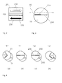
- Fig. 1 represents a magnetic random access memory (MRAM) cell 1 comprising a magnetic tunnel junction 2 formed from a read magnetic layer 21 having a read magnetization direction 210, a tunnel barrier layer 22, and a storage layer 23 having a storage magnetization direction 233, 234.
- a first current line 4 in electrical communication with the magnetic tunnel junction 2 is disposed at one end of the magnetic tunnel junction 2 and is arranged to provide a heating current 31 in the magnetic tunnel junction 2.
- the MRAM cell 1 can further comprise a second current line 5 adapted to pass a field current 41 such as to generate a magnetic field 42.
- the second current line 5 is disposed at the same end of the magnetic tunnel junction 2 as the first current line 4, but could also be disposed on the opposite end.
- the first current line 4 can fulfill both the function of passing the heating current 31 and the function of passing the field current 41.
- the storage layer 23 is represented by a synthetic storage layer comprising a first storage ferromagnetic layer 230 having a first storage magnetization 233, and a second storage ferromagnetic layer 231 having a second storage magnetization 234.
- the magnetization of the two storage ferromagnetic layers 233, 234 are coupled in an anti-parallel direction due to the presence of a storage anti-parallel coupling layer 232.
- the storage layer 23 comprising the two storage ferromagnetic layers 230, 231 and the storage anti-parallel coupling layer 232 will be referred to as a synthetic antiferromagnet or "SAF" storage layer 23.
- the two storage ferromagnetic layers 230, 231 can be made of a CoFe, CoFeB or NiFe alloy and have a thickness typically comprised between about 1.5 nm and about 4 nm.
- the storage anti-parallel coupling layer 232 can be realized using a non-magnetic separating layer with material selected from a group consisting of ruthenium, chromium, rhenium, iridium, rhodium, silver, copper and yttrium.
- the storage anti-parallel coupling layer 232 is made of ruthenium and has a thickness typically comprised between about 0.6 nm and 2nm, preferably between 0.6nm and about 0.9 nm or between about 1.6nm and about 2nm.
- the read magnetization 210 of the read layer 21 is fixed relative to the first and second storage magnetization 233, 234.
- Such read layer is also called reference layer.
- the read layer 21 can also be a synthetic antiferromagnetic read layer comprising a first read ferromagnetic layer and a second read ferromagnetic layer, the two reference ferromagnetic layers being coupled in an anti-parallel direction with a read anti-parallel coupling layer.
- the first read ferromagnetic layer, in contact with the tunnel barrier layer 22, can be made of a CoFeB alloy while the second read ferromagnetic layer can be made of a CoFe alloy.
- the second read ferromagnetic layers can have a thickness typically comprised between about 1 nm and about 4 nm.
- the read anti-parallel coupling layer can be made of Ru and have a thickness typically comprised between about 0.6 nm and about 2nm, preferably between about 0.6nm and about 0.9 nm or between about 1.6nm and about 2nm.
- the magnetic tunnel junction 2 further comprises an antiferromagnetic read layer 25 pinning the read magnetization 210, such that the read magnetization 210 of the read layer 21 is fixed relative to the first and second storage magnetization 233, 234.
- the antiferromagnetic read layer 25 is preferably disposed adjacent to the read layer 21 on its side opposed to the tunnel barrier layer 22.
- the antiferromagnetic read layer 25 is preferably formed of a Mn based alloy, for example, comprising one of PtMn, NiMn, IrMn and FeMn, and is arranged such as to pin the read magnetization 210.
- the tunnel barrier layer 22 can be an insulating layer, for example, made from an oxide selected in the group including among others aluminum oxides Al 2 O 3 and magnesium oxides MgO.
- the SAF storage layer 23 has its magnetization direction 233, 234 being adjustable in a reversible manner during a write operation.
- the write operation can comprise passing the field current 41 in the second current line 5 (or in the first current line 4) such as to generate an external magnetic field 42 adapted to align the storage magnetization 233, 234 according to the magnitude and polarity of the field current 41.
- the field current 41 is shown pointing within the page and the magnetic field 42 is represented by the arrow pointing toward the left.
- the write operation also comprises a step of heating the magnetic tunnel junction 2, for example, by passing the heating current 31 through the magnetic tunnel junction 2 via the first current line 4.
- the MRAM cell 1 can further comprises a selection transistor (not represented) such that the heating current 31 is passed when the selection transistor is in a saturated mode.
- the second storage magnetization 234 is aligned in the external magnetic field 42 once the magnetic tunnel junction 2 has reached a predetermined high temperature threshold.
- the first storage magnetization 233 is oriented in accordance with its coupling with the second storage layer magnetization 234 through the anti-parallel coupling layer 232.
- the magnetic tunnel junction 2 is then cooled to a low temperature threshold at which the second storage magnetization 234 is frozen in its written state. This can be performed with the selection transistor being is the blocked mode such that the field current does not pass through the magnetic tunnel junction 2.
- Such a thermally-assisted switching write operation is described in more details in U.S. Patent No. 6,950,335 .
- the magnetic tunnel junction 2 further comprises an antiferromagnetic storage layer 24 adjacent to the SAF storage layer 23 on its side opposed to the tunnel barrier layer 22.
- the antiferromagnetic storage layer 24 is adapted to exchange-couple the SAF storage layer 23 such as to pin, or fix, the second storage magnetization 234 at a temperature at the low temperature threshold, At the high temperature threshold the second storage magnetization 234 is no longer pinned by antiferromagnetic storage layer 24 and can be freely adjusted under the external magnetic field 42.
- the antiferromagnetic storage layer 24 can be made of a manganese-based alloy, such as IrMn or FeMn, or any other suitable materials.
- the high temperature threshold is typically at or above a temperature of about 150°C.
- Figs. 2 and 3 represent a schematic cross-section of the SAF storage layer 23 with the first and second storage ferromagnetic layer 230, 231 viewed from the side ( Fig. 2 ) and from top ( Fig. 3 ), according to an embodiment. More particularly, the first storage magnetization 233 is represented oriented antiparallel with the second storage magnetization 234 due to the magnetic coupling of the two storage magnetizations 233, 234 through the storage anti-parallel coupling layer 232. In the example of Figs. 2 and 3 , the first and second storage magnetization 233, 234 are aligned substantially parallel with an anisotropy axis 60 corresponding to the easy axis of the first and second storage ferromagnetic layer 230, 231.
- Fig. 6 represents a magnetization curve of the SAF storage layer 23 comprising the first and second storage ferromagnetic layer 230, 231 for the case where the external magnetic field 42 is applied along the anisotropy axis 60.
- Symbol B denote the magnitude of the magnetic field 42
- symbol M denotes the magnetization values of the first and second storage magnetization 233, 234.
- the magnetization curve shows a hysteresis loop delimited by spin-flop value B SF of the magnetic field 42.
- the first storage magnetization 233 is no more antiparallel with the second storage magnetization but forms a predetermined angle ⁇ with the second storage magnetization (see Figs.
- the first storage magnetization 233 becomes oriented substantially parallel to the second storage magnetization 234.
- the magnitude of the magnetic field 42 required to orients the first storage magnetization 233 substantially parallel to the second storage magnetization 234 is referred to as the saturation magnetic field B SAT .
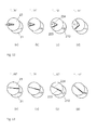
- Figs. 4a to d illustrate arrangements of the first and second storage magnetization 233, 234 when the external magnetic field 42 is applied along the anisotropy axis 60, and the magnetic tunnel junction 2 is heated at the predetermined high temperature threshold.
- the read layer 21 is also represented in Figs. 4a to d by the offset circle showing the corresponding read magnetization 210. It is assumed that the second storage magnetization 234 has a greater magnitude and is thus oriented with the magnetic field 42, while the first storage magnetization 233 is oriented due to the coupling effect of the coupling layer 232.
- Figs. 5a to 5d illustrate arrangements of the first and second storage magnetization 233, 234 after cooling the magnetic tunnel junction 2 to the low temperature threshold and in the absence of the applied external magnetic field 42.
- the magnetic field 42 is applied with a magnitude that is below a spin-flop value B SF of the first and second storage magnetization 233, 234, shown by the portions b and c of the magnetization curve of Fig. 6 , respectively. More particularly, in Fig. 4b the magnetic field 42 is applied in the same direction as the one of the read magnetization 210 and orients the second storage magnetization 234 substantially parallel with the read magnetization 210. The first storage magnetization 233 becomes oriented substantially antiparallel with the read magnetization 210 due to the coupling effect of the coupling layer 232.
- the arrangement of the first and second storage magnetization 233, 234 remains unchanged ( Fig. 5b ).
- This arrangement corresponds to a high magnetoresistance of the tunnel magnetic junction 2 and to a predetermined state level, for example a first state level indicated by the numeral "11" in Fig. 5b .
- the magnetic field 42 is oriented in a direction opposite to the one of the example of Fig. 4b , such that the first storage magnetization 233 becomes oriented substantially parallel with the read magnetization 210.
- the magnetic field 42 is applied with a magnitude that is equal or exceeds the spin-flop value B SF , shown by the portions a and d of the magnetization curve of Fig. 6 , respectively.
- the second storage magnetization 234 is oriented with the magnetic field 42 and form a predetermined angle ⁇ with the first storage magnetization 233 through the storage anti-parallel coupling layer 232.
- the predetermined angle ⁇ is maximal when the magnitude of the magnetic field 42 corresponds to the spin-flop value B SF , and diminishes when the magnitude of the magnetic field 42 exceeds the spin-flop value B SP.
- the first and second storage magnetization 233, 234 become substantially parallel when the magnetic field 42 is applied at the saturation value B SAT .
- the second storage magnetization 234 is oriented with the magnetic field 42 having a magnitude being above the spin-flop value B SF and below the saturation value B SAT . and in a direction opposed to the one of the read magnetization 210 (portion a of the magnetization curve of Fig. 6 ).
- the magnetic field 42 orients the first and second storage magnetization 233, 234 at an angle of about 180° - ⁇ /2 with the read magnetization 210.
- the second storage magnetization 234 is also oriented with the magnetic field 42 having a magnitude being above the spin-flop value B SF and below the saturation value B SAT , but in the same direction as the one of the read magnetization 210 (portion d of the magnetization curve of Fig. 6 ).
- the magnetic field 42 orients the first and second storage magnetization 233, 234 at an angle of about ⁇ /2 with the read magnetization 210.
- the orientation of the first storage magnetization 233 becomes oriented antiparallel with the second storage magnetization 234 making an angle of 180° - ⁇ /2 with the read magnetization 210 ( Fig. 5d ).
- This arrangement corresponds to a second intermediate value of the magnetoresistance of the tunnel magnetic junction 2 and to a fourth state level indicated by the numeral "10" in Fig. 5d .
- the method disclosed herein allows for storing at least four distinct state levels in the MRAM cell 1 by applying the magnetic field 42 in two opposite directions and a magnitude below the spin-flop value B SF of the first and second storage magnetization 233, 234, and with a magnitude at and above the spin-flop value B SF .
- the step of heating the magnetic tunnel junction 2 when performing the write operation as described above allows for writing the different state levels using only the second current line 5 to generate a magnetic field.
- Another current line typically disposed orthogonal with the second current line 5 as in most conventional MRAM cells is therefore not needed.
- the first current line 4 fulfills both the function of passing the heating current 31 and the function of passing the field current 41, only the first current line 4 is required for writing the different state levels to the MRAM cell 1.
- the strength of the magnetic coupling within the SAF storage layer 23 depends on the thickness of the nonmagnetic storage anti-parallel coupling layer 232. Consequently, a larger angle ⁇ can then be obtained when the magnetic field 42 is applied with a magnitude at and above the spin-flop value B SF , by tuning the thickness of the storage anti-parallel coupling layer 232.
- a read operation can then be performed for reading the written state levels.
- a read current 32 is selectively passed through the magnetic tunnel junction 2 via the first current line 4, for example by setting the selection transistor in the saturated mode, to measure junction resistance (R MTJ ) of the magnetic tunnel junction 2.
- the resistance state can be determined by comparing the measured junction resistance (R MTJ ) with a reference resistance measured for a reference MRAM cell (not represented).
- Figs. 7 and 8 represent a schematic cross-section of the SAF layer 23 with the first and second storage ferromagnetic layer 230, 231 viewed from the side ( Fig. 7 ) and from top ( Fig. 8 ), according to the present embodiment.
- the first storage magnetization 233 is represented antiparallel with the second storage magnetization 234 due to the coupling of the two storage magnetizations 233, 234 through the storage anti parallel coupling layer 232, the first and second storage magnetization 233, 234 being aligned substantially parallel with a first anisotropy axis 60.
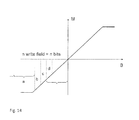
- the corresponding magnetization curve shown in Fig. 11 does not show an opening of the hysteresis loop and the sudden net rise in the magnetization M as in the magnetization curve of Fig. 6 . Instead, the magnetization M varies linearly with the magnitude B of the applied field 42 until the applied field 42 reaches the saturation magnetic field H SAT .
- FIGs 9a to 9d The arrangements of the first and second storage magnetization 233, 234 when applying the external magnetic field 42 is represented in Figs 9a to 9d .
- Figs. 10a to 10d illustrate arrangements of the first and second storage magnetization 233, 234 after the magnetic tunnel junction 2 has been cooled to the low temperature threshold and in the absence of the applied external magnetic field 42.
- the magnetic field 42 is applied in a direction opposed to the one of the read magnetization 210 (toward the left on Fig. 9 ).
- the second storage magnetization 234 is moved downward under the action of the magnetic field 42 from its initial upward position along the second anisotropy axis 60.
- the first storage magnetization 233 is moved upward from its initial downward position, such that the first storage magnetisation 233 makes an angle ⁇ with the second storage magnetization 234.
- the value of the angle ⁇ decreases when increasing the magnitude of the applied magnetic field 42.
- the magnitude of the magnetic field 42 is higher than the one in Fig. 9b and the resulting angle ⁇ between the first and second storage magnetization 233, 234 is also smaller.
- the first storage magnetization 233 becomes almost antiparallel with the read magnetization 210.
- the first and second storage magnetization 233, 234 substantially antiparallel with the read magnetization 210 can be obtained when the applied field 42 has a magnitude corresponding to the saturation value B SAT .
- the first storage magnetization 233 becomes oriented substantially antiparallel with the second storage magnetization 234 ( Figs. 10a and 10b ) and forms an angle ⁇ /2 with the read magnetization 210.
- the angle ⁇ /2 is small (almost parallel with the read magnetization 210) resulting in a low value of the magnetoresistance of the tunnel magnetic junction 2, corresponding to a first state level indicated by the numeral "00" in Fig. 10a .
- the configuration of Fig. 10b yields a first intermediate value of the magnetoresistance of the tunnel magnetic junction 2 and to a second state level indicated by the numeral "01".
- the magnetic field 42 is applied substantially in a direction opposed to the one of Figs. 9a and 9b , such that the first and second storage magnetization 233, 234 are oriented toward the read magnetization 210.
- the first storage magnetization 233 becomes oriented at an angle of 180° - ⁇ /2 with the read magnetization 210. This results in a second intermediate value of the magnetoresistance of the tunnel magnetic junction 2 and to a third state level indicated by the numeral "10".
- Fig. 9c and 9d the magnetic field 42 is applied substantially in a direction opposed to the one of Figs. 9a and 9b , such that the first and second storage magnetization 233, 234 are oriented toward the read magnetization 210.
- the value of angle of 180° - ⁇ /2 is such that the first storage magnetization 233 becomes oriented almost antiparallel with the read magnetization 210, resulting in a high value of the magnetoresistance of the tunnel magnetic junction 2 and to a fourth state level indicated by the numeral "11".
- the value of the angle ⁇ angle between the the first and second storage magnetization 233, 234 decreases continuously with increasing the magnitude of the applied magnetic field 42 until the magnitude of the magnetic field 42 reaches the saturation value B SAT where the first and second storage magnetization 233, 234 are substantially parallel and oriented in the same direction.
- FIG. 12a to 12d This is illustrated in the embodiment of Figs. 12a to 12d , where several arrangements of the first and second storage magnetization 233, 234 are obtained when the magnetic field 42 is applied oriented toward the left in Fig 12 , and with increasing magnitude corresponding to the portions (a) to (d) of the of magnetization curve shown in Fig. 14 .
- the angle ⁇ between the first and second storage magnetization 233, 234 varies from a value close to 0° when the magnetic field 42 is applied at the saturation value B SAT (portion "a" of magnetization curve of Fig. 11 ) to a value close to 180° when the magnetic field 42 is applied at a magnitude close to zero.
- Figs. 12a to 12d show the configurations where the angle ⁇ between the first and second storage magnetization 233 234 increases with the decreasing magnetic fields 42 as shown by the portions (b) to (d) of the magnetization curve of Fig. 14 , respectively.
- Figs. 13a to 13d illustrate arrangements of the first and second storage magnetization 233, 234 after the magnetic tunnel junction 2 has been cooled to the low temperature threshold and in the absence of the applied external magnetic field 42.
- the first storage magnetization 233 is oriented almost parallel to the read magnetization 210 corresponding to the low value of the magnetoresistance of the tunnel magnetic junction 2 and to the first state level indicated by the numeral "00".
- the increasing angle ⁇ /2 between the first storage magnetization 233 and the read magnetization 214 corresponds to the four different state levels indicated by the numeral "01, "10” and "11".
- the magnetic tunnel junction 2 can thus be written with a plurality of state levels by varying the magnitude of the applied magnetic field 42 from the saturation value B SAT and below, along the corresponding magnetisation curve.
- the slope of the magnetization curve of Fig. 14 can be varied by varying the magnetic coupling between the first and second storage magnetization 233, 234. This can be achieved by varying the thickness of the storage anti-parallel coupling layer 232 or/and by modifying the material and thicknesses of the first and second storage ferromagnetic layer 230, 231. For example, a magnetization curve with a steeper slope can be obtained by increasing the thicknesses of the first and second storage layers 230, 231.
- the magnetization curve of Fig. 14 having a steep slope allows for larger increments of resistance in the different applied magnetic field 42, such that the writing of the different state levels can be made with smaller magnetic field 42.
- the read layer 21 is made of a low coercivity, soft ferromagnetic material.
- the ferromagnetic materials include typically iron, cobalt nickel or their alloys.
- the read layer 21 is not exchange biased and the read magnetization 210 has a direction that can be varied freely, for example, due to thermal agitation and thus, its magnetization can be freely aligned in a magnetic field.
- the read operation can be based on a self-referenced read operation as described in patent application EP2276034 by the present applicant. More particularly, the read operation can comprise, in a first read cycle, passing a first read field current having a first polarity in the second current line 5 (or possible the first current line 4).
- the first read field current induces a first read magnetic field capable of aligning the read magnetization 210 in a first aligned magnetization direction according to the first polarity of the first read field current.
- the first aligned magnetization direction of the read layer 21 is then compared with the written state level by passing the read current though the magnetic tunnel junction 2 via the current line 4, such as to measure a first junction resistance R 1 of the magnetic tunnel junction 2.
- Such self-referenced read operation further comprises a second read cycle, comprising passing a second read field current having a second polarity in the second current line 5 (or first current line 4), such as to induce a second read magnetic field capable of aligning the read magnetization 210 in a second aligned magnetization direction according to the second polarity of the second read field current.
- the second aligned magnetization directions of the read layer 21 is then compared with the written state level by passing the read current though the magnetic current junction 2 via the current line 4, such as to measure a second junction resistance R 2 of the magnetic tunnel junction 2.
- the written state level can then be determined by determining a difference between the first and second resistance value H 1 , R 2 .
- the first read current has an alternating polarity and induces an alternating first read magnetic field aligning the read magnetization 210 alternatively, in accordance to the alternating polarity of the first read current.
- the alternating first read current aligns alternatively the read magnetization 210 without switching completely its magnetization. Consequently, the measured first resistance value R 1 varies alternatively with the varying read magnetization 210 and the written state level can be determined by comparing the varying first resistance value R 1 with the alternating first read current.
Abstract
Description
- The present invention concerns a method for writing to a plurality of data bits in a magnetic random access memory (MRAM) cell.
- Memory devices that employ variable resistance materials include resistive random access memories (RRAM), phase change random access memories (PRAM), ferroelectric random access memories (FRAM), magnetic random access memories (MRAM), etc. The nonvolatile memory devices listed above may store data based on a variation in the resistance of a variable resistance material (RRAM), a phase change material having amorphous and crystalline states (PRAM), a ferroelectric material having different polarization states (FRAM), and/or a magnetic tunnel junction film of a ferroelectric material having different magnetized states (MRAM).
- Devices based on MRAM have experiencing a renewed interest since magnetic tunnel junctions demonstrated a strong magnetoresistance at ambient temperature. MRAM present many advantages such as high writing and reading speeds (down to a few nanoseconds) non volatility, and insensitivity to ionizing radiations. MRAM comprising a so-called "magnetoresistance effect" or GMR have been first proposed. Such MRAMs were made by stacking several metal layers being alternatively magnetic and nonmagnetic. The GMR element disadvantageously requires large magnetic fields to be applied and thus requires large currents for writing and reading information.
- The development of MRAM cells with a magnetic tunnel junction has allowed a significant increase in the performances and operating mode of these MRAMs. Such MRAM cells are described in
U.S. Pat. No. 5,640,343 . Such MRAM cell typically comprises a magnetic tunnel junction having a tunneling barrier layer between a first ferromagnetic layer and a second ferromagnetic layer. The magnetic tunnel junction is electrically connected at one end to a first current line and, to its other end, to a selection CMOS transistor. The MRAM cell further comprises a second current line disposed orthogonal to the first current line. - The first and second ferromagnetic layers typically have different coercivities and are preferentially made from 3d metals such as Fe, Co,Ni, and their alloys, possibly containing boron in order to amorphize the ferromagnetic layers arid to flatten their interfaces. The tunneling barrier layer is typically a thin insulating layer of alumina (Al2O3) or MgO. Each ferromagnetic layer can be coupled with an anti-ferromagnetic layer (not shown), whose function is to trap the ferromagnetic layer it couples, so that the magnetization of the coupled ferromagnetic layer is pinned and cannot rotate freely.
- During a write operation of the conventional MRAM cell, the selection transistor is set in a blocked mode such that no current passes through the magnetic tunnel junction. A first field current is passed in the first current line generating a first magnetic field, and a second field current is passed in the second current line generating a second magnetic field. The first and second magnetic fields are adapted such as to switch the magnetization direction of the second magnetic layer, thus writing the MRAM cell. In an array comprising a plurality of the MRAM cell, only the
cell 1 being located at the intersection of the first and second current line is being written, or addressed, under the effect of the combined first and second magnetic fields. The write operation is then selective. - During a read operation, a read current is selectively passed through the magnetic tunnel junction of the written cell by setting the selection transistor of this
cell 1 in the saturated mode such as to measure a junction resistance of the magnetic tunnel junction. The magnetoresistance of theMRAM cell 1 can be determined by comparing the measured junction resistance with a reference resistance measured for a reference MRAM cell. A low measured junction resistance (or level state "0") corresponds to the magnetization direction of the second ferromagnetic layer being oriented parallel to the magnetization direction of the first ferromagnetic layer, while a high measured junction resistance (or level state "1") corresponds to the magnetization direction of the second ferromagnetic layer being oriented antiparallel to the magnetization direction of the first ferromagnetic layer. The difference between the value of the high and low junction resistance, or the tunnel magnetoresistance, depends on the material composing the ferromagnetic layers and possibly on heat treatment performed on these ferromagnetic layers. A tunnel magnetoresistance of more than 70% can be reached with a suitable choice of materials and and/or heat treatment. - MRAM cells with a multilevel state write operation has also been proposed, allowing for writing more than the two level states "0" and "1" as described above. Such a MRAM cell with a multilevel state write operation is disclosed in
U.S. Pat. No. 6,950,335 . Here, the magnetization of the second ferromagnetic layer, or storage layer, can be oriented in any intermediate direction between the direction parallel and the direction antiparallel to the magnetization direction of the first ferromagnetic layer, or reference layer. Orienting the magnetization of the storage layer in the intermediate directions can be achieved by generating magnetic fields with appropriate relative intensity along the perpendicular directions of the first and second current line - The present disclosure describes a method for writing and reading a plurality of data bits to art magnetic random access memory (MRAM) cell that can comprise a magnetic tunnel junction formed from a read magnetic layer having a read magnetization, a tunnel barrier layer, and a storage layer that can be freely oriented at a high temperature threshold; the storage layer comprising a first storage ferromagnetic layer having a first storage magnetization, a second storage ferromagnetic layer having a second storage magnetization, and a storage anti-parallel coupling layer magnetically coupling the first and second storage magnetization; the method comprising:
- heating the magnetic tunnel junction at the high temperature threshold;
- orienting the first and second storage magnetization; and
- cooling the magnetic tunnel junction to a low temperature threshold to freeze the first and second storage magnetization; wherein
- said orienting the first and second storage magnetization comprises the first storage magnetization forming a predetermined angle with respect to the second storage magnetization such as to reach a predetermined resistance state level of the magnetic tunnel junction determined by the orientation of the first and second storage magnetization relative to the read magnetization; and wherein cooling the magnetic tunnel junction comprises freezing the second storage magnetization at the predetermined angle.
- In an embodiment, orienting the first and second storage magnetization can comprise applying an external magnetic field by passing a field current in the current line, the predetermined angle being determined according to the magnitude and direction of the magnetic field.
- In another embodiment, applying an external magnetic field can be performed substantially pararllel to the anisotropy axis of the first and second storage magnetization.
- In yet another embodiment, said magnitude of the magnetic field can be below a spin-flop value or equal or exceeding the spin-flop value.
- In yet another embodiment, applying an external magnetic field can be performed substantially orthogonal to the anisotropy axis of the first and second storage magnetization.
- In yet another embodiment, said magnitude of the magnetic field can be varied from a saturation value of the first and second storage magnetization, and below.
- In yet another embodiment, the magnetic tunnel junction can further comprise an antiferromagnetic storage layer adapted to pin the first and second storage magnetization at the low temperature threshold.
- In yet another embodiment, the read magnetization of the read layer can be fixed relative to the storage magnetization direction; and can further comprise passing a read current through the magnetic tunnel junction to measure a junction resistance of the magnetic tunnel junction.
- In yet another embodiment, the magnetic tunnel junction can further comprise an antiferromagnetic read layer pinning the read magnetization.
- In yet another embodiment, the read magnetization of the read layer can have a direction that can be varied freely; the method can further comprise aligning the read magnetization in a first aligned direction such as to measure a first junction resistance of the magnetic tunnel junction; aligning the read magnetization in a second aligned direction such as to measure a second junction resistance of the magnetic tunnel junction; and determining a difference between the first and second junction resistance.
- In yet another embodiment, aligning the read magnetization in a first aligned direction can comprise passing a first read current having a first polarity in the current line; and aligning the read magnetization in a second aligned direction can comprise passing a second read current having a second polarity in the current line.
- In yet another embodiment, the first storage ferromagnetic layer and the second storage ferromagnetic layer can be made from a CoFe, CoFeB or NiFe alloy and the storage anti-parallel coupling layer can be made from a non-magnetic layer with material selected from a group consisting of ruthenium, chromium, rhenium, iridium, rhodium, silver, copper and yttrium.
- In yet another embodiment, wherein the first and second storage ferromagnetic layer can have a thickness comprised between about 1.5 nm and about 4 nm.
- In yet another embodiment, the storage anti-parallel coupling layer can be made of ruthenium and can have a thickness comprised between about 0.6 nm and about 2nm, preferably between about 0.6nm and about 0.9 nm or between about 1.6nm and about 2nm.
- In yet another embodiment, the saturation field value of the first and second storage magnetization can be varied by varying thickness of the storage anti-parallel coupling layer or by varying thickness of the first and second storage layer.
- The method disclosed herein allows for storing at least four distinct state levels in the MRAM cell. The writing operation can be performed with the MRAM cell comprising only one current line for generating a single magnetic field. Another current line, typically disposed orthogonal with the current line as in most conventional MRAM cells is not needed.
- The invention will be better understood with the aid of the description of an embodiment given by way of example and illustrated by the figures, in which:
-
Fig. 1 represents a magnetic random access memory (MRAM) cell comprising a magnetic tunnel junction formed from a read magnetic layer, a tunnel barrier layer, and a storage layer, according to an embodiment; -
Figs. 2 and 3 represent a schematic cross-section of the storage layer viewed from the side (Fig. 2 ) and from top (Fig. 3 ), according to an embodiment; -
Figs. 4a to 4d illustrate arrangements of the first and second storage layers in the presence of an external magnetic field and when heating the magnetic tunnel junction, according to an embodiment; -
Figs. 5a to 5d illustrate arrangements of the first and second storage magnetization in the absence of the magnetic field and after cooling the magnetic tunnel junction, according to an embodiment; -
Fig. 6 represents a magnetization curve of the storage layer according to an embodiment; -
Figs. 7 and 8 represent a schematic cross-section of the storage layer viewed from the side (Fig. 7 ) and from top (Fig. 8 ), according to another embodiment; -
Figs. 9a to 9d illustrate arrangements of the first and second storage layers in the presence of an external magnetic field and when heating the magnetic tunnel junction, according to another embodiment; -
Figs. 10a to 10d illustrate arrangement of the first and second storage magnetization in the absence of the magnetic field and after cooling the magnetic tunnel junction, according to another embodiment; -
Fig. 11 represents a magnetization curve of the storage layer according to another embodiment; -
Figs. 12a to 12d illustrate arrangements of the first and second storage layers in the presence of an external magnetic field and when heating the magnetic tunnel junction, according to yet another embodiment; -
Figs. 13a to 13d illustrate arrangements of the first and second storage magnetization in the absence of the magnetic field and after cooling the magnetic tunnel junction, according to yet another embodiment; and -
Fig. 14 represents a magnetization curve of the storage layer according to yet another embodiment. -
Fig. 1 represents a magnetic random access memory (MRAM)cell 1 comprising amagnetic tunnel junction 2 formed from a readmagnetic layer 21 having a readmagnetization direction 210, atunnel barrier layer 22, and astorage layer 23 having astorage magnetization direction current line 4 in electrical communication with themagnetic tunnel junction 2 is disposed at one end of themagnetic tunnel junction 2 and is arranged to provide a heating current 31 in themagnetic tunnel junction 2. TheMRAM cell 1 can further comprise a secondcurrent line 5 adapted to pass a field current 41 such as to generate amagnetic field 42. In the example ofFig. 1 , the secondcurrent line 5 is disposed at the same end of themagnetic tunnel junction 2 as the firstcurrent line 4, but could also be disposed on the opposite end. Alternatively, the firstcurrent line 4 can fulfill both the function of passing the heating current 31 and the function of passing the field current 41. - In the embodiment of
Fig. 1 , thestorage layer 23 is represented by a synthetic storage layer comprising a first storageferromagnetic layer 230 having afirst storage magnetization 233, and a second storageferromagnetic layer 231 having asecond storage magnetization 234. The magnetization of the two storageferromagnetic layers anti-parallel coupling layer 232. Thestorage layer 23 comprising the two storageferromagnetic layers anti-parallel coupling layer 232 will be referred to as a synthetic antiferromagnet or "SAF"storage layer 23. The two storageferromagnetic layers anti-parallel coupling layer 232 can be realized using a non-magnetic separating layer with material selected from a group consisting of ruthenium, chromium, rhenium, iridium, rhodium, silver, copper and yttrium. Preferably, the storageanti-parallel coupling layer 232 is made of ruthenium and has a thickness typically comprised between about 0.6 nm and 2nm, preferably between 0.6nm and about 0.9 nm or between about 1.6nm and about 2nm. - In an embodiment, the read
magnetization 210 of the readlayer 21 is fixed relative to the first andsecond storage magnetization Fig. 1 , theread layer 21 can also be a synthetic antiferromagnetic read layer comprising a first read ferromagnetic layer and a second read ferromagnetic layer, the two reference ferromagnetic layers being coupled in an anti-parallel direction with a read anti-parallel coupling layer. In this configuration, the first read ferromagnetic layer, in contact with thetunnel barrier layer 22, can be made of a CoFeB alloy while the second read ferromagnetic layer can be made of a CoFe alloy. The second read ferromagnetic layers can have a thickness typically comprised between about 1 nm and about 4 nm. The read anti-parallel coupling layer can be made of Ru and have a thickness typically comprised between about 0.6 nm and about 2nm, preferably between about 0.6nm and about 0.9 nm or between about 1.6nm and about 2nm. - In an embodiment, the
magnetic tunnel junction 2 further comprises anantiferromagnetic read layer 25 pinning the readmagnetization 210, such that the readmagnetization 210 of the readlayer 21 is fixed relative to the first andsecond storage magnetization antiferromagnetic read layer 25 is preferably disposed adjacent to theread layer 21 on its side opposed to thetunnel barrier layer 22. Theantiferromagnetic read layer 25 is preferably formed of a Mn based alloy, for example, comprising one of PtMn, NiMn, IrMn and FeMn, and is arranged such as to pin the readmagnetization 210. - The
tunnel barrier layer 22 can be an insulating layer, for example, made from an oxide selected in the group including among others aluminum oxides Al2O3 and magnesium oxides MgO. - According to an embodiment, the
SAF storage layer 23 has itsmagnetization direction magnetic field 42 adapted to align thestorage magnetization Fig. 1 , the field current 41 is shown pointing within the page and themagnetic field 42 is represented by the arrow pointing toward the left. - In an embodiment, the write operation also comprises a step of heating the
magnetic tunnel junction 2, for example, by passing the heating current 31 through themagnetic tunnel junction 2 via the firstcurrent line 4. TheMRAM cell 1 can further comprises a selection transistor (not represented) such that the heating current 31 is passed when the selection transistor is in a saturated mode. During the write operation, thesecond storage magnetization 234 is aligned in the externalmagnetic field 42 once themagnetic tunnel junction 2 has reached a predetermined high temperature threshold. Thefirst storage magnetization 233 is oriented in accordance with its coupling with the secondstorage layer magnetization 234 through theanti-parallel coupling layer 232. Themagnetic tunnel junction 2 is then cooled to a low temperature threshold at which thesecond storage magnetization 234 is frozen in its written state. This can be performed with the selection transistor being is the blocked mode such that the field current does not pass through themagnetic tunnel junction 2. Such a thermally-assisted switching write operation is described in more details inU.S. Patent No. 6,950,335 . - In the example of
Fig. 1 , themagnetic tunnel junction 2 further comprises anantiferromagnetic storage layer 24 adjacent to theSAF storage layer 23 on its side opposed to thetunnel barrier layer 22. Theantiferromagnetic storage layer 24 is adapted to exchange-couple theSAF storage layer 23 such as to pin, or fix, thesecond storage magnetization 234 at a temperature at the low temperature threshold, At the high temperature threshold thesecond storage magnetization 234 is no longer pinned byantiferromagnetic storage layer 24 and can be freely adjusted under the externalmagnetic field 42. Theantiferromagnetic storage layer 24 can be made of a manganese-based alloy, such as IrMn or FeMn, or any other suitable materials. The high temperature threshold is typically at or above a temperature of about 150°C. -
Figs. 2 and 3 represent a schematic cross-section of theSAF storage layer 23 with the first and second storageferromagnetic layer Fig. 2 ) and from top (Fig. 3 ), according to an embodiment. More particularly, thefirst storage magnetization 233 is represented oriented antiparallel with thesecond storage magnetization 234 due to the magnetic coupling of the twostorage magnetizations anti-parallel coupling layer 232. In the example ofFigs. 2 and 3 , the first andsecond storage magnetization anisotropy axis 60 corresponding to the easy axis of the first and second storageferromagnetic layer -
Fig. 6 represents a magnetization curve of theSAF storage layer 23 comprising the first and second storageferromagnetic layer magnetic field 42 is applied along theanisotropy axis 60. Symbol B denote the magnitude of themagnetic field 42 and symbol M denotes the magnetization values of the first andsecond storage magnetization magnetic field 42. When the magnitude of themagnetic field 42 is increased above a value corresponding to the spin-flop value BSF, thefirst storage magnetization 233 is no more antiparallel with the second storage magnetization but forms a predetermined angle α with the second storage magnetization (seeFigs. 4a and 4b ). When the magnetic field is further increase, thefirst storage magnetization 233 becomes oriented substantially parallel to thesecond storage magnetization 234. The magnitude of themagnetic field 42 required to orients thefirst storage magnetization 233 substantially parallel to thesecond storage magnetization 234 is referred to as the saturation magnetic field BSAT. -
Figs. 4a to d illustrate arrangements of the first andsecond storage magnetization magnetic field 42 is applied along theanisotropy axis 60, and themagnetic tunnel junction 2 is heated at the predetermined high temperature threshold. Theread layer 21 is also represented inFigs. 4a to d by the offset circle showing thecorresponding read magnetization 210. It is assumed that thesecond storage magnetization 234 has a greater magnitude and is thus oriented with themagnetic field 42, while thefirst storage magnetization 233 is oriented due to the coupling effect of thecoupling layer 232.Figs. 5a to 5d illustrate arrangements of the first andsecond storage magnetization magnetic tunnel junction 2 to the low temperature threshold and in the absence of the applied externalmagnetic field 42. - In
Figs. 4b and c themagnetic field 42 is applied with a magnitude that is below a spin-flop value BSF of the first andsecond storage magnetization Fig. 6 , respectively. More particularly, inFig. 4b themagnetic field 42 is applied in the same direction as the one of the readmagnetization 210 and orients thesecond storage magnetization 234 substantially parallel with the readmagnetization 210. Thefirst storage magnetization 233 becomes oriented substantially antiparallel with the readmagnetization 210 due to the coupling effect of thecoupling layer 232. After cooling themagnetic tunnel junction 2 and in the absence of the applied externalmagnetic field 42, the arrangement of the first andsecond storage magnetization Fig. 5b ). This arrangement corresponds to a high magnetoresistance of the tunnelmagnetic junction 2 and to a predetermined state level, for example a first state level indicated by the numeral "11" inFig. 5b . InFig. 4c , themagnetic field 42 is oriented in a direction opposite to the one of the example ofFig. 4b , such that thefirst storage magnetization 233 becomes oriented substantially parallel with the readmagnetization 210. This corresponds to a low magnetoresistance of the tunnelmagnetic junction 2 and to a second state level indicated by the numeral "00" inFig. 5c . - In
Figs. 4a and d themagnetic field 42 is applied with a magnitude that is equal or exceeds the spin-flop value BSF, shown by the portions a and d of the magnetization curve ofFig. 6 , respectively. Here, thesecond storage magnetization 234 is oriented with themagnetic field 42 and form a predetermined angle α with thefirst storage magnetization 233 through the storageanti-parallel coupling layer 232. The predetermined angle α is maximal when the magnitude of themagnetic field 42 corresponds to the spin-flop value BSF, and diminishes when the magnitude of themagnetic field 42 exceeds the spin-flop value BSP. The first andsecond storage magnetization magnetic field 42 is applied at the saturation value BSAT. - More particularly, in the example of the
Fig. 4a thesecond storage magnetization 234 is oriented with themagnetic field 42 having a magnitude being above the spin-flop value BSF and below the saturation value BSAT. and in a direction opposed to the one of the read magnetization 210 (portion a of the magnetization curve ofFig. 6 ). Here, themagnetic field 42 orients the first andsecond storage magnetization magnetization 210. After themagnetic tunnel junction 2 has been cooled to the low temperature threshold and in the absence of the applied externalmagnetic field 42, the orientation of thesecond storage magnetisation 234 remains unchanged while thefirst storage magnetization 233 becomes oriented antiparallel with thesecond storage magnetization 234, thus making an angle α/2 with the read magnetization 210 (Fig. 5a ). This arrangement corresponds to a first intermediate value of the magnetoresistance of the tunnelmagnetic junction 2 and to a third state level indicated by the numeral "01" inFig. 5a . - In the example of the
Fig. 4d , thesecond storage magnetization 234 is also oriented with themagnetic field 42 having a magnitude being above the spin-flop value BSF and below the saturation value BSAT, but in the same direction as the one of the read magnetization 210 (portion d of the magnetization curve ofFig. 6 ). In this case, themagnetic field 42 orients the first andsecond storage magnetization magnetization 210. After themagnetic tunnel junction 2 has been cooled to the low temperature threshold and in the absence of the applied externalmagnetic field 42, the orientation of thefirst storage magnetization 233 becomes oriented antiparallel with thesecond storage magnetization 234 making an angle of 180° - α/2 with the read magnetization 210 (Fig. 5d ). This arrangement corresponds to a second intermediate value of the magnetoresistance of the tunnelmagnetic junction 2 and to a fourth state level indicated by the numeral "10" inFig. 5d . - The method disclosed herein allows for storing at least four distinct state levels in the
MRAM cell 1 by applying themagnetic field 42 in two opposite directions and a magnitude below the spin-flop value BSF of the first andsecond storage magnetization - The step of heating the
magnetic tunnel junction 2 when performing the write operation as described above allows for writing the different state levels using only the secondcurrent line 5 to generate a magnetic field. Another current line, typically disposed orthogonal with the secondcurrent line 5 as in most conventional MRAM cells is therefore not needed. Moreover, in the case the firstcurrent line 4 fulfills both the function of passing the heating current 31 and the function of passing the field current 41, only the firstcurrent line 4 is required for writing the different state levels to theMRAM cell 1. - As known in the art, the strength of the magnetic coupling within the
SAF storage layer 23 depends on the thickness of the nonmagnetic storageanti-parallel coupling layer 232. Consequently, a larger angle α can then be obtained when themagnetic field 42 is applied with a magnitude at and above the spin-flop value BSF, by tuning the thickness of the storageanti-parallel coupling layer 232. - A read operation can then be performed for reading the written state levels. During the read operation, a read current 32 is selectively passed through the
magnetic tunnel junction 2 via the firstcurrent line 4, for example by setting the selection transistor in the saturated mode, to measure junction resistance (RMTJ) of themagnetic tunnel junction 2. The resistance state can be determined by comparing the measured junction resistance (RMTJ) with a reference resistance measured for a reference MRAM cell (not represented). - In another embodiment represented in
Figs. 7 to 11 , themagnetic field 42 is applied substantially orthogonal with theanisotropy axis 60 ofSAF storage layer 23, while themagnetic tunnel junction 2 is heated at the predetermined high temperature threshold. More particularly,Figs. 7 and 8 represent a schematic cross-section of theSAF layer 23 with the first and second storageferromagnetic layer Fig. 7 ) and from top (Fig. 8 ), according to the present embodiment. Thefirst storage magnetization 233 is represented antiparallel with thesecond storage magnetization 234 due to the coupling of the twostorage magnetizations parallel coupling layer 232, the first andsecond storage magnetization first anisotropy axis 60. - In the case the
magnetic field 42 is applied substantially orthogonal with theanisotropy axis 60, the corresponding magnetization curve shown inFig. 11 does not show an opening of the hysteresis loop and the sudden net rise in the magnetization M as in the magnetization curve ofFig. 6 . Instead, the magnetization M varies linearly with the magnitude B of the appliedfield 42 until the appliedfield 42 reaches the saturation magnetic field HSAT. - The arrangements of the first and
second storage magnetization magnetic field 42 is represented inFigs 9a to 9d .Figs. 10a to 10d illustrate arrangements of the first andsecond storage magnetization magnetic tunnel junction 2 has been cooled to the low temperature threshold and in the absence of the applied externalmagnetic field 42. - More particularly, in
Figs. 9a and 9b , themagnetic field 42 is applied in a direction opposed to the one of the read magnetization 210 (toward the left onFig. 9 ). Thesecond storage magnetization 234 is moved downward under the action of themagnetic field 42 from its initial upward position along thesecond anisotropy axis 60. Thefirst storage magnetization 233 is moved upward from its initial downward position, such that thefirst storage magnetisation 233 makes an angle α with thesecond storage magnetization 234. - The value of the angle α decreases when increasing the magnitude of the applied
magnetic field 42. InFig. 9a , the magnitude of themagnetic field 42 is higher than the one inFig. 9b and the resulting angle α between the first andsecond storage magnetization Fig. 9a , thefirst storage magnetization 233 becomes almost antiparallel with the readmagnetization 210. The first andsecond storage magnetization magnetization 210 can be obtained when the appliedfield 42 has a magnitude corresponding to the saturation value BSAT. - After cooling the
magnetic tunnel junction 2 to the low temperature threshold and in the absence of the applied externalmagnetic field 42, thefirst storage magnetization 233 becomes oriented substantially antiparallel with the second storage magnetization 234 (Figs. 10a and 10b ) and forms an angle α/2 with the readmagnetization 210. In the configuration ofFig. 10a , the angle α/2 is small (almost parallel with the read magnetization 210) resulting in a low value of the magnetoresistance of the tunnelmagnetic junction 2, corresponding to a first state level indicated by the numeral "00" inFig. 10a . The configuration ofFig. 10b yields a first intermediate value of the magnetoresistance of the tunnelmagnetic junction 2 and to a second state level indicated by the numeral "01". - In
Figs. 9c and 9d , themagnetic field 42 is applied substantially in a direction opposed to the one ofFigs. 9a and 9b , such that the first andsecond storage magnetization magnetization 210. After cooling themagnetic tunnel junction 2 to the low temperature threshold and in the absence of the applied externalmagnetic field 42, thefirst storage magnetization 233 becomes oriented at an angle of 180° - α/2 with the readmagnetization 210. This results in a second intermediate value of the magnetoresistance of the tunnelmagnetic junction 2 and to a third state level indicated by the numeral "10". InFig. 10d , the value of angle of 180° - α/2 is such that thefirst storage magnetization 233 becomes oriented almost antiparallel with the readmagnetization 210, resulting in a high value of the magnetoresistance of the tunnelmagnetic junction 2 and to a fourth state level indicated by the numeral "11". - In fact, in the embodiment of
Figs. 7 to 11 , where themagnetic field 42 is applied substantially orthogonal with theanisotropy axis 60, the value of the angle α angle between the the first andsecond storage magnetization magnetic field 42 until the magnitude of themagnetic field 42 reaches the saturation value BSAT where the first andsecond storage magnetization - This is illustrated in the embodiment of
Figs. 12a to 12d , where several arrangements of the first andsecond storage magnetization magnetic field 42 is applied oriented toward the left inFig 12 , and with increasing magnitude corresponding to the portions (a) to (d) of the of magnetization curve shown inFig. 14 . - More particularly, the angle α between the first and
second storage magnetization magnetic field 42 is applied at the saturation value BSAT (portion "a" of magnetization curve ofFig. 11 ) to a value close to 180° when themagnetic field 42 is applied at a magnitude close to zero.Figs. 12a to 12d show the configurations where the angle α between the first andsecond storage magnetization 233 234 increases with the decreasingmagnetic fields 42 as shown by the portions (b) to (d) of the magnetization curve ofFig. 14 , respectively.Figs. 13a to 13d illustrate arrangements of the first andsecond storage magnetization magnetic tunnel junction 2 has been cooled to the low temperature threshold and in the absence of the applied externalmagnetic field 42. - In
Fig. 13a , thefirst storage magnetization 233 is oriented almost parallel to the readmagnetization 210 corresponding to the low value of the magnetoresistance of the tunnelmagnetic junction 2 and to the first state level indicated by the numeral "00". As shown inFig. 13a to 13d , the increasing angle α/2 between thefirst storage magnetization 233 and the read magnetization 214 corresponds to the four different state levels indicated by the numeral "01, "10" and "11". According to the embodiment ofFigs. 12 to 14 , themagnetic tunnel junction 2 can thus be written with a plurality of state levels by varying the magnitude of the appliedmagnetic field 42 from the saturation value BSAT and below, along the corresponding magnetisation curve. - The slope of the magnetization curve of
Fig. 14 can be varied by varying the magnetic coupling between the first andsecond storage magnetization anti-parallel coupling layer 232 or/and by modifying the material and thicknesses of the first and second storageferromagnetic layer Fig. 14 having a steep slope allows for larger increments of resistance in the different appliedmagnetic field 42, such that the writing of the different state levels can be made with smallermagnetic field 42. - In another embodiment not represented, the
read layer 21 is made of a low coercivity, soft ferromagnetic material. The ferromagnetic materials include typically iron, cobalt nickel or their alloys. In contrast to thestorage layer 23, theread layer 21 is not exchange biased and the readmagnetization 210 has a direction that can be varied freely, for example, due to thermal agitation and thus, its magnetization can be freely aligned in a magnetic field. - Here, the read operation can be based on a self-referenced read operation as described in patent application
EP2276034 by the present applicant. More particularly, the read operation can comprise, in a first read cycle, passing a first read field current having a first polarity in the second current line 5 (or possible the first current line 4). The first read field current induces a first read magnetic field capable of aligning the readmagnetization 210 in a first aligned magnetization direction according to the first polarity of the first read field current. The first aligned magnetization direction of the readlayer 21 is then compared with the written state level by passing the read current though themagnetic tunnel junction 2 via thecurrent line 4, such as to measure a first junction resistance R1 of themagnetic tunnel junction 2. - Such self-referenced read operation further comprises a second read cycle, comprising passing a second read field current having a second polarity in the second current line 5 (or first current line 4), such as to induce a second read magnetic field capable of aligning the read
magnetization 210 in a second aligned magnetization direction according to the second polarity of the second read field current. The second aligned magnetization directions of the readlayer 21 is then compared with the written state level by passing the read current though the magneticcurrent junction 2 via thecurrent line 4, such as to measure a second junction resistance R2 of themagnetic tunnel junction 2. The written state level can then be determined by determining a difference between the first and second resistance value H1, R2. - In another embodiment not represented, the first read current has an alternating polarity and induces an alternating first read magnetic field aligning the read
magnetization 210 alternatively, in accordance to the alternating polarity of the first read current. Preferably, the alternating first read current aligns alternatively the readmagnetization 210 without switching completely its magnetization. Consequently, the measured first resistance value R1 varies alternatively with the varyingread magnetization 210 and the written state level can be determined by comparing the varying first resistance value R1 with the alternating first read current. -
- 1
- MRAM cell
- 2
- magnetic tunnel junction
- 21
- read layer
- 22
- tunnel barrier layer
- 23
- storage layer,SAF storage layer
- 210
- read magnetization
- 230
- first storage ferromagnetic layer
- 231
- second storage ferromagnetic layer
- 232
- storage anti-parallel coupling layer
- 233
- first storage magnetization
- 234
- second storage magnetization
- 24
- antiferromagnetic storage layer
- 25
- antiferromagnetic read layer
- 4
- first current line
- 31
- heating current
- 32
- read current
- 5
- second current line
- 41
- field current
- 42
- external magnetic field
- 60
- anisotropy axis
- α
- angle
- B
- value of the external magnetic field
- BSAT
- saturation value of the external magnetic field
- BSF
- spin-flop value of the external magnetic field.
- M
- resulting magnetization
Claims (15)
- Method for writing and reading a plurality of data bits to a magnetic random access memory (MRAM) cell (1) comprising
a magnetic tunnel junction (2) formed from a read magnetic layer (21) having a read magnetization (210), a tunnel barrier layer (22), and a storage layer (23);
the storage layer (23) that can be freely oriented at a high temperature threshold comprising a first storage ferromagnetic layer (230) having a first storage magnetization (233), a second storage ferromagnetic layer (231) having a second storage magnetization (234), and a storage anti-parallel coupling layer (232) magnetically coupling the first and second storage magnetization (233, 234); the method comprising:heating the magnetic tunnel junction (2) to the high temperature threshold;orienting the first and second storage magnetization (233, 234);
andcooling the magnetic tunnel junction (2) to a low temperature threshold to freeze the second storage magnetization (234); characterized in thatsaid orienting the first and second storage magnetization (233, 734) comprises the first storage magnetization (233) forming a predetermined angle (α) with respect to the second storage magnetization (234) such as to reach a predetermined state resistance level of the magnetic tunnel junction (2) determined by the orientation of the first storage magnetization (233) relative to the read magnetization (210); and in that cooling the magnetic tunnel junction (2) comprises freezing the second storage magnetization (234) at the predetermined angle (α). - The method according to claim 1, wherein
orienting the first and second storage magnetization (233, 234) comprises applying an external magnetic field (42), the predetermined angle (α) being determined according to the magnitude and direction of the magnetic field (42). - The method according to claim 2, wherein
applying an external magnetic field (42) is performed substantially parallel to the anisotropy axis (60) of the first and second storage magnetization (233, 234). - The method according to claim 3, wherein
said magnitude of the magnetic field (42) is below a spin-flop value (BSF), or equal or exceeding the spin-flop value (BSF). - The method according to claim 2, wherein
applying an external magnetic field (42) is performed substantially orthogonal to the anisotropy axis (60) of the first and second storage magnetization (233, 234). - The method according to claim 5, wherein
said magnitude of the magnetic field (42) is varied from a saturation value (BSAT) of the first and second storage magnetization (233, 234), and below. - The method according to any one of the claims from 1 to 6,
wherein the magnetic tunnel junction (2) further comprises an antiferromagnetic storage layer (24) adapted to pin the second storage magnetization (234) at the low temperature threshold. - The method according to any one of the claims from 1 to 7,
wherein
the read magnetization (210) of the read layer (21) is fixed relative to the storage magnetization direction (233, 234); and further comprising passing a read current through the magnetic tunnel junction (2) to measure a junction resistance (RMTJ) of the magnetic funnel junction (2). - The method according to claim 8, wherein
the magnetic tunnel junction (2) further comprises an antiferromagnetic read layer (25) pinning the read magnetization (210). - The method according to any one of the claims from 1 to 7,
wherein the read magnetization (210) of the read layer (21) has a direction that can be varied freely; the method further comprising aligning the read magnetization (210) in a first aligned direction such as to measure a first junction resistance (R1) of the magnetic tunnel junction (2); aligning the read magnetization (210) in a second aligned direction such as to measure a second junction resistance (R2) of the magnetic tunnel junction (2); and determining a difference between the first and second junction resistance (R1, R2). - The method according to claim 10, wherein
aligning the read magnetization (210) in a first aligned direction comprises passing a first read current having a first polarity in the current line (4); and aligning the read magnetization (210) in a second aligned direction comprises passing a second read current having a second polarity in the current line (4). - The method according to any one of the claims from 1 to 11, wherein the first storage ferromagnetic layer (230) and the second storage ferromagnetic layer (231) are made from a CoFe, CoFeB or NiFe alloy and the storage anti-parallel coupling layer (232) is made from a non-magnetic layer with material selected from a group consisting of ruthenium, chromium, rhenium, iridium, rhodium, silver, copper and yttrium.
- The method according to any one of the claims from 1 to 12, wherein the first and second storage ferromagnetic layer (230, 231) has a thickness comprised between about 1.5 nm and about 4 nm.
- The method according to any one of the claims from 1 to 13, wherein the storage anti-parallel coupling layer (232) is made of ruthenium and has a thickness comprised between about 0.6 nm and about 2nm, preferably between about 0.6nm and about 0.9 nm or between about 1.6nm and about 2nm.
- The method according to claim 14, wherein
the saturation value (BSAT) of the first and second storage magnetization (233, 234) is varied by varying thickness of the storage anti-parallel coupling layer (232) or by varying thickness of the first and second storage layer.
Priority Applications (5)
| Application Number | Priority Date | Filing Date | Title |
|---|---|---|---|
| EP11290239.0A EP2528060B1 (en) | 2011-05-23 | 2011-05-23 | Multibit cell with synthetic storage layer |
| US13/475,215 US8503225B2 (en) | 2011-05-23 | 2012-05-18 | Multibit cell with synthetic storage layer |
| TW101117980A TW201250681A (en) | 2011-05-23 | 2012-05-21 | Multibit cell with synthetic storage layer |
| RU2012121194/02A RU2573457C2 (en) | 2011-05-23 | 2012-05-22 | Multibit cell with synthetic storage layer |
| JP2012116154A JP5879198B2 (en) | 2011-05-23 | 2012-05-22 | Multi-bit cell with synthetic storage layer |
Applications Claiming Priority (1)
| Application Number | Priority Date | Filing Date | Title |
|---|---|---|---|
| EP11290239.0A EP2528060B1 (en) | 2011-05-23 | 2011-05-23 | Multibit cell with synthetic storage layer |
Publications (2)
| Publication Number | Publication Date |
|---|---|
| EP2528060A1 true EP2528060A1 (en) | 2012-11-28 |
| EP2528060B1 EP2528060B1 (en) | 2016-12-14 |
Family
ID=44562688
Family Applications (1)
| Application Number | Title | Priority Date | Filing Date |
|---|---|---|---|
| EP11290239.0A Active EP2528060B1 (en) | 2011-05-23 | 2011-05-23 | Multibit cell with synthetic storage layer |
Country Status (5)
| Country | Link |
|---|---|
| US (1) | US8503225B2 (en) |
| EP (1) | EP2528060B1 (en) |
| JP (1) | JP5879198B2 (en) |
| RU (1) | RU2573457C2 (en) |
| TW (1) | TW201250681A (en) |
Cited By (2)
| Publication number | Priority date | Publication date | Assignee | Title |
|---|---|---|---|---|
| EP2725580A1 (en) * | 2012-10-25 | 2014-04-30 | Crocus Technology S.A. | Thermally assisted MRAM cell and method for writing a plurality of bits in the MRAM cell |
| EP3002758A1 (en) * | 2014-10-03 | 2016-04-06 | Crocus Technology S.A. | Self-referenced MRAM cell and magnetic field sensor comprising the self-referenced MRAM cell |
Families Citing this family (5)
| Publication number | Priority date | Publication date | Assignee | Title |
|---|---|---|---|---|
| EP2276034B1 (en) * | 2009-07-13 | 2016-04-27 | Crocus Technology S.A. | Self-referenced magnetic random access memory cell |
| CN103927681A (en) * | 2013-01-15 | 2014-07-16 | 行将企业股份有限公司 | Vehicle auction management system |
| EP2760025B1 (en) * | 2013-01-23 | 2019-01-02 | Crocus Technology S.A. | TAS-MRAM element with low writing temperature |
| US9406870B2 (en) * | 2014-04-09 | 2016-08-02 | International Business Machines Corporation | Multibit self-reference thermally assisted MRAM |
| US10439133B2 (en) | 2017-03-13 | 2019-10-08 | Samsung Electronics Co., Ltd. | Method and system for providing a magnetic junction having a low damping hybrid free layer |
Citations (7)
| Publication number | Priority date | Publication date | Assignee | Title |
|---|---|---|---|---|
| US5640343A (en) | 1996-03-18 | 1997-06-17 | International Business Machines Corporation | Magnetic memory array using magnetic tunnel junction devices in the memory cells |
| WO2003021689A1 (en) * | 2001-08-31 | 2003-03-13 | Nve Corporation | Antiparallel magnetoresistive memory cells |
| US20050105355A1 (en) * | 2001-11-12 | 2005-05-19 | Hubert Brueckl | Method for homogeneously magnetizing an exchange-coupled layer system of a digital magnetic memory location device |
| US6950335B2 (en) | 2001-11-16 | 2005-09-27 | Commissariat A L'energie Atomique | Magnetic tunnel junction magnetic device, memory and writing and reading methods using said device |
| US20090010088A1 (en) * | 2007-07-02 | 2009-01-08 | Industrial Technology Research Institute | Data reading circuit of toggle magnetic memory |
| US20090073748A1 (en) * | 2007-09-17 | 2009-03-19 | Ulrich Klostermann | Integrated Circuits; Methods for Operating an Integrating Circuit; Memory Modules |
| EP2276034A2 (en) | 2009-07-13 | 2011-01-19 | Crocus Technology S.A. | Self-referenced magnetic random access memory cell |
Family Cites Families (7)
| Publication number | Priority date | Publication date | Assignee | Title |
|---|---|---|---|---|
| JP2001084756A (en) * | 1999-09-17 | 2001-03-30 | Sony Corp | Magnetization driving method, magnetic functional element and magnetic device |
| SG115462A1 (en) * | 2002-03-12 | 2005-10-28 | Inst Data Storage | Multi-stage per cell magnetoresistive random access memory |
| US7095646B2 (en) * | 2002-07-17 | 2006-08-22 | Freescale Semiconductor, Inc. | Multi-state magnetoresistance random access cell with improved memory storage density |
| US7110287B2 (en) * | 2004-02-13 | 2006-09-19 | Grandis, Inc. | Method and system for providing heat assisted switching of a magnetic element utilizing spin transfer |
| RU2367057C2 (en) * | 2007-10-31 | 2009-09-10 | Государственное образовательное учреждение высшего профессионального образования "Московский Инженерно-Физический Институт (государственный университет)" | Method of forming structures of magnetic tunnel barriers for magnetoresistive random access magnetic memory and structure of magnetic tunnel barrier for magnetoresistive random access magnetic memory (versions) |
| FR2925747B1 (en) * | 2007-12-21 | 2010-04-09 | Commissariat Energie Atomique | MAGNETIC MEMORY WITH THERMALLY ASSISTED WRITING |
| EP2447949B1 (en) * | 2010-10-26 | 2016-11-30 | Crocus Technology | Multi level magnetic element |
-
2011
- 2011-05-23 EP EP11290239.0A patent/EP2528060B1/en active Active
-
2012
- 2012-05-18 US US13/475,215 patent/US8503225B2/en active Active
- 2012-05-21 TW TW101117980A patent/TW201250681A/en unknown
- 2012-05-22 JP JP2012116154A patent/JP5879198B2/en active Active
- 2012-05-22 RU RU2012121194/02A patent/RU2573457C2/en active
Patent Citations (7)
| Publication number | Priority date | Publication date | Assignee | Title |
|---|---|---|---|---|
| US5640343A (en) | 1996-03-18 | 1997-06-17 | International Business Machines Corporation | Magnetic memory array using magnetic tunnel junction devices in the memory cells |
| WO2003021689A1 (en) * | 2001-08-31 | 2003-03-13 | Nve Corporation | Antiparallel magnetoresistive memory cells |
| US20050105355A1 (en) * | 2001-11-12 | 2005-05-19 | Hubert Brueckl | Method for homogeneously magnetizing an exchange-coupled layer system of a digital magnetic memory location device |
| US6950335B2 (en) | 2001-11-16 | 2005-09-27 | Commissariat A L'energie Atomique | Magnetic tunnel junction magnetic device, memory and writing and reading methods using said device |
| US20090010088A1 (en) * | 2007-07-02 | 2009-01-08 | Industrial Technology Research Institute | Data reading circuit of toggle magnetic memory |
| US20090073748A1 (en) * | 2007-09-17 | 2009-03-19 | Ulrich Klostermann | Integrated Circuits; Methods for Operating an Integrating Circuit; Memory Modules |
| EP2276034A2 (en) | 2009-07-13 | 2011-01-19 | Crocus Technology S.A. | Self-referenced magnetic random access memory cell |
Cited By (9)
| Publication number | Priority date | Publication date | Assignee | Title |
|---|---|---|---|---|
| EP2725580A1 (en) * | 2012-10-25 | 2014-04-30 | Crocus Technology S.A. | Thermally assisted MRAM cell and method for writing a plurality of bits in the MRAM cell |
| WO2014063939A1 (en) | 2012-10-25 | 2014-05-01 | Crocus Technology | Thermally assisted mram cell and method for writing a plurality of bits in the mram cell |
| US9754653B2 (en) | 2012-10-25 | 2017-09-05 | Crocus Technology Sa | Thermally assisted multi-level MRAM cell and method for writing a plurality of bits in the MRAM cell |
| EP3002758A1 (en) * | 2014-10-03 | 2016-04-06 | Crocus Technology S.A. | Self-referenced MRAM cell and magnetic field sensor comprising the self-referenced MRAM cell |
| WO2016050614A1 (en) * | 2014-10-03 | 2016-04-07 | Crocus Technology Sa | Self-referenced mram cell and magnetic field sensor comprising the self-referenced mram cell |
| CN107076809A (en) * | 2014-10-03 | 2017-08-18 | 克罗科斯科技公司 | Self-reference mram cell and the magnetic field sensor for including the self-reference mram cell |
| JP2017533419A (en) * | 2014-10-03 | 2017-11-09 | クロッカス・テクノロジー・ソシエテ・アノニム | Self-referenced MRAM cell and magnetic field sensor having the self-referenced MRAM cell |
| US9905283B2 (en) | 2014-10-03 | 2018-02-27 | Crocus Technology Sa | Self-referenced MRAM cell and magnetic field sensor comprising the self-referenced MRAM cell |
| CN107076809B (en) * | 2014-10-03 | 2019-11-26 | 克罗科斯科技公司 | Self-reference mram cell and magnetic field sensor including the self-reference mram cell |
Also Published As
| Publication number | Publication date |
|---|---|
| EP2528060B1 (en) | 2016-12-14 |
| JP5879198B2 (en) | 2016-03-08 |
| TW201250681A (en) | 2012-12-16 |
| US20120300539A1 (en) | 2012-11-29 |
| RU2573457C2 (en) | 2016-01-20 |
| JP2012248835A (en) | 2012-12-13 |
| US8503225B2 (en) | 2013-08-06 |
| RU2012121194A (en) | 2013-11-27 |
Similar Documents
| Publication | Publication Date | Title |
|---|---|---|
| US9837602B2 (en) | Spin-orbit torque bit design for improved switching efficiency | |
| US8331141B2 (en) | Multibit cell of magnetic random access memory with perpendicular magnetization | |
| US8988934B2 (en) | Multibit cell of magnetic random access memory with perpendicular magnetization | |
| EP2575135B1 (en) | Magnetic random access memory (MRAM) cell and method for reading the MRAM cell using a self-referenced read operation | |
| EP2466586B1 (en) | Multibit magnetic random access memory cell with improved read margin | |
| US8503225B2 (en) | Multibit cell with synthetic storage layer | |
| EP2725580B1 (en) | Thermally assisted MRAM cell and method for writing a plurality of bits in the MRAM cell | |
| EP2608208B1 (en) | Self-referenced MRAM cell and method for writing the cell using a spin transfer torque write operation | |
| US9799384B2 (en) | Multi-bit MRAM cell and method for writing and reading to such MRAM cell | |
| US9679624B2 (en) | Magnetic random access memory (MRAM) cell with low power consumption | |
| US9305628B2 (en) | Self-referenced magnetic random access memory (MRAM) and method for writing to the MRAM cell with increased reliability and reduced power consumption | |
| CN106463169B (en) | Self reference multidigit mram cell with synthetic anti-ferromagnetic accumulation layer | |
| KR20120130737A (en) | Multibit Cell with Synthetic Storage Layer |
Legal Events
| Date | Code | Title | Description |
|---|---|---|---|
| PUAI | Public reference made under article 153(3) epc to a published international application that has entered the european phase |
Free format text: ORIGINAL CODE: 0009012 |
|
| AK | Designated contracting states |
Kind code of ref document: A1 Designated state(s): AL AT BE BG CH CY CZ DE DK EE ES FI FR GB GR HR HU IE IS IT LI LT LU LV MC MK MT NL NO PL PT RO RS SE SI SK SM TR |
|
| AX | Request for extension of the european patent |
Extension state: BA ME |
|
| 17P | Request for examination filed |
Effective date: 20130429 |
|
| RIC1 | Information provided on ipc code assigned before grant |
Ipc: G11C 11/16 20060101AFI20141022BHEP Ipc: G11C 11/56 20060101ALI20141022BHEP |
|
| 17Q | First examination report despatched |
Effective date: 20141121 |
|
| GRAP | Despatch of communication of intention to grant a patent |
Free format text: ORIGINAL CODE: EPIDOSNIGR1 |
|
| INTG | Intention to grant announced |
Effective date: 20160713 |
|
| GRAS | Grant fee paid |
Free format text: ORIGINAL CODE: EPIDOSNIGR3 |
|
| GRAA | (expected) grant |
Free format text: ORIGINAL CODE: 0009210 |
|
| AK | Designated contracting states |
Kind code of ref document: B1 Designated state(s): AL AT BE BG CH CY CZ DE DK EE ES FI FR GB GR HR HU IE IS IT LI LT LU LV MC MK MT NL NO PL PT RO RS SE SI SK SM TR |
|
| REG | Reference to a national code |
Ref country code: GB Ref legal event code: FG4D |
|
| REG | Reference to a national code |
Ref country code: CH Ref legal event code: EP |
|
| REG | Reference to a national code |
Ref country code: IE Ref legal event code: FG4D |
|
| REG | Reference to a national code |
Ref country code: AT Ref legal event code: REF Ref document number: 854241 Country of ref document: AT Kind code of ref document: T Effective date: 20170115 |
|
| REG | Reference to a national code |
Ref country code: DE Ref legal event code: R096 Ref document number: 602011033341 Country of ref document: DE |
|
| PG25 | Lapsed in a contracting state [announced via postgrant information from national office to epo] |
Ref country code: LV Free format text: LAPSE BECAUSE OF FAILURE TO SUBMIT A TRANSLATION OF THE DESCRIPTION OR TO PAY THE FEE WITHIN THE PRESCRIBED TIME-LIMIT Effective date: 20161214 |
|
| REG | Reference to a national code |
Ref country code: LT Ref legal event code: MG4D |
|
| REG | Reference to a national code |
Ref country code: NL Ref legal event code: MP Effective date: 20161214 |
|
| PG25 | Lapsed in a contracting state [announced via postgrant information from national office to epo] |
Ref country code: LT Free format text: LAPSE BECAUSE OF FAILURE TO SUBMIT A TRANSLATION OF THE DESCRIPTION OR TO PAY THE FEE WITHIN THE PRESCRIBED TIME-LIMIT Effective date: 20161214 Ref country code: NO Free format text: LAPSE BECAUSE OF FAILURE TO SUBMIT A TRANSLATION OF THE DESCRIPTION OR TO PAY THE FEE WITHIN THE PRESCRIBED TIME-LIMIT Effective date: 20170314 Ref country code: GR Free format text: LAPSE BECAUSE OF FAILURE TO SUBMIT A TRANSLATION OF THE DESCRIPTION OR TO PAY THE FEE WITHIN THE PRESCRIBED TIME-LIMIT Effective date: 20170315 Ref country code: SE Free format text: LAPSE BECAUSE OF FAILURE TO SUBMIT A TRANSLATION OF THE DESCRIPTION OR TO PAY THE FEE WITHIN THE PRESCRIBED TIME-LIMIT Effective date: 20161214 |
|
| REG | Reference to a national code |
Ref country code: AT Ref legal event code: MK05 Ref document number: 854241 Country of ref document: AT Kind code of ref document: T Effective date: 20161214 |
|
| REG | Reference to a national code |
Ref country code: FR Ref legal event code: PLFP Year of fee payment: 7 |
|
| PG25 | Lapsed in a contracting state [announced via postgrant information from national office to epo] |
Ref country code: HR Free format text: LAPSE BECAUSE OF FAILURE TO SUBMIT A TRANSLATION OF THE DESCRIPTION OR TO PAY THE FEE WITHIN THE PRESCRIBED TIME-LIMIT Effective date: 20161214 Ref country code: RS Free format text: LAPSE BECAUSE OF FAILURE TO SUBMIT A TRANSLATION OF THE DESCRIPTION OR TO PAY THE FEE WITHIN THE PRESCRIBED TIME-LIMIT Effective date: 20161214 Ref country code: FI Free format text: LAPSE BECAUSE OF FAILURE TO SUBMIT A TRANSLATION OF THE DESCRIPTION OR TO PAY THE FEE WITHIN THE PRESCRIBED TIME-LIMIT Effective date: 20161214 |
|
| PG25 | Lapsed in a contracting state [announced via postgrant information from national office to epo] |
Ref country code: NL Free format text: LAPSE BECAUSE OF FAILURE TO SUBMIT A TRANSLATION OF THE DESCRIPTION OR TO PAY THE FEE WITHIN THE PRESCRIBED TIME-LIMIT Effective date: 20161214 |
|
| PG25 | Lapsed in a contracting state [announced via postgrant information from national office to epo] |
Ref country code: CZ Free format text: LAPSE BECAUSE OF FAILURE TO SUBMIT A TRANSLATION OF THE DESCRIPTION OR TO PAY THE FEE WITHIN THE PRESCRIBED TIME-LIMIT Effective date: 20161214 Ref country code: EE Free format text: LAPSE BECAUSE OF FAILURE TO SUBMIT A TRANSLATION OF THE DESCRIPTION OR TO PAY THE FEE WITHIN THE PRESCRIBED TIME-LIMIT Effective date: 20161214 Ref country code: RO Free format text: LAPSE BECAUSE OF FAILURE TO SUBMIT A TRANSLATION OF THE DESCRIPTION OR TO PAY THE FEE WITHIN THE PRESCRIBED TIME-LIMIT Effective date: 20161214 Ref country code: SK Free format text: LAPSE BECAUSE OF FAILURE TO SUBMIT A TRANSLATION OF THE DESCRIPTION OR TO PAY THE FEE WITHIN THE PRESCRIBED TIME-LIMIT Effective date: 20161214 Ref country code: IS Free format text: LAPSE BECAUSE OF FAILURE TO SUBMIT A TRANSLATION OF THE DESCRIPTION OR TO PAY THE FEE WITHIN THE PRESCRIBED TIME-LIMIT Effective date: 20170414 |
|
| PG25 | Lapsed in a contracting state [announced via postgrant information from national office to epo] |
Ref country code: ES Free format text: LAPSE BECAUSE OF FAILURE TO SUBMIT A TRANSLATION OF THE DESCRIPTION OR TO PAY THE FEE WITHIN THE PRESCRIBED TIME-LIMIT Effective date: 20161214 Ref country code: LU Free format text: LAPSE BECAUSE OF NON-PAYMENT OF DUE FEES Effective date: 20170531 Ref country code: BE Free format text: LAPSE BECAUSE OF FAILURE TO SUBMIT A TRANSLATION OF THE DESCRIPTION OR TO PAY THE FEE WITHIN THE PRESCRIBED TIME-LIMIT Effective date: 20161214 Ref country code: SM Free format text: LAPSE BECAUSE OF FAILURE TO SUBMIT A TRANSLATION OF THE DESCRIPTION OR TO PAY THE FEE WITHIN THE PRESCRIBED TIME-LIMIT Effective date: 20161214 Ref country code: IT Free format text: LAPSE BECAUSE OF FAILURE TO SUBMIT A TRANSLATION OF THE DESCRIPTION OR TO PAY THE FEE WITHIN THE PRESCRIBED TIME-LIMIT Effective date: 20161214 Ref country code: AT Free format text: LAPSE BECAUSE OF FAILURE TO SUBMIT A TRANSLATION OF THE DESCRIPTION OR TO PAY THE FEE WITHIN THE PRESCRIBED TIME-LIMIT Effective date: 20161214 Ref country code: PL Free format text: LAPSE BECAUSE OF FAILURE TO SUBMIT A TRANSLATION OF THE DESCRIPTION OR TO PAY THE FEE WITHIN THE PRESCRIBED TIME-LIMIT Effective date: 20161214 Ref country code: PT Free format text: LAPSE BECAUSE OF FAILURE TO SUBMIT A TRANSLATION OF THE DESCRIPTION OR TO PAY THE FEE WITHIN THE PRESCRIBED TIME-LIMIT Effective date: 20170414 Ref country code: BG Free format text: LAPSE BECAUSE OF FAILURE TO SUBMIT A TRANSLATION OF THE DESCRIPTION OR TO PAY THE FEE WITHIN THE PRESCRIBED TIME-LIMIT Effective date: 20170314 |
|
| REG | Reference to a national code |
Ref country code: DE Ref legal event code: R097 Ref document number: 602011033341 Country of ref document: DE |
|
| PLBE | No opposition filed within time limit |
Free format text: ORIGINAL CODE: 0009261 |
|
| STAA | Information on the status of an ep patent application or granted ep patent |
Free format text: STATUS: NO OPPOSITION FILED WITHIN TIME LIMIT |
|
| 26N | No opposition filed |
Effective date: 20170915 |
|
| PG25 | Lapsed in a contracting state [announced via postgrant information from national office to epo] |
Ref country code: DK Free format text: LAPSE BECAUSE OF FAILURE TO SUBMIT A TRANSLATION OF THE DESCRIPTION OR TO PAY THE FEE WITHIN THE PRESCRIBED TIME-LIMIT Effective date: 20161214 |
|
| REG | Reference to a national code |
Ref country code: CH Ref legal event code: PL |
|
| PG25 | Lapsed in a contracting state [announced via postgrant information from national office to epo] |
Ref country code: MC Free format text: LAPSE BECAUSE OF FAILURE TO SUBMIT A TRANSLATION OF THE DESCRIPTION OR TO PAY THE FEE WITHIN THE PRESCRIBED TIME-LIMIT Effective date: 20161214 |
|
| REG | Reference to a national code |
Ref country code: IE Ref legal event code: MM4A |
|
| PG25 | Lapsed in a contracting state [announced via postgrant information from national office to epo] |
Ref country code: LI Free format text: LAPSE BECAUSE OF NON-PAYMENT OF DUE FEES Effective date: 20170531 Ref country code: CH Free format text: LAPSE BECAUSE OF NON-PAYMENT OF DUE FEES Effective date: 20170531 Ref country code: SI Free format text: LAPSE BECAUSE OF FAILURE TO SUBMIT A TRANSLATION OF THE DESCRIPTION OR TO PAY THE FEE WITHIN THE PRESCRIBED TIME-LIMIT Effective date: 20161214 |
|
| PG25 | Lapsed in a contracting state [announced via postgrant information from national office to epo] |
Ref country code: LU Free format text: LAPSE BECAUSE OF NON-PAYMENT OF DUE FEES Effective date: 20170523 |
|
| PG25 | Lapsed in a contracting state [announced via postgrant information from national office to epo] |
Ref country code: IE Free format text: LAPSE BECAUSE OF NON-PAYMENT OF DUE FEES Effective date: 20170523 |
|
| REG | Reference to a national code |
Ref country code: FR Ref legal event code: PLFP Year of fee payment: 8 |
|
| PG25 | Lapsed in a contracting state [announced via postgrant information from national office to epo] |
Ref country code: MT Free format text: LAPSE BECAUSE OF NON-PAYMENT OF DUE FEES Effective date: 20170523 |
|
| PG25 | Lapsed in a contracting state [announced via postgrant information from national office to epo] |
Ref country code: HU Free format text: LAPSE BECAUSE OF FAILURE TO SUBMIT A TRANSLATION OF THE DESCRIPTION OR TO PAY THE FEE WITHIN THE PRESCRIBED TIME-LIMIT; INVALID AB INITIO Effective date: 20110523 |
|
| PG25 | Lapsed in a contracting state [announced via postgrant information from national office to epo] |
Ref country code: CY Free format text: LAPSE BECAUSE OF NON-PAYMENT OF DUE FEES Effective date: 20161214 |
|
| PG25 | Lapsed in a contracting state [announced via postgrant information from national office to epo] |
Ref country code: MK Free format text: LAPSE BECAUSE OF FAILURE TO SUBMIT A TRANSLATION OF THE DESCRIPTION OR TO PAY THE FEE WITHIN THE PRESCRIBED TIME-LIMIT Effective date: 20161214 |
|
| REG | Reference to a national code |
Ref country code: DE Ref legal event code: R082 Ref document number: 602011033341 Country of ref document: DE Representative=s name: BECK & ROESSIG EUROPEAN PATENT ATTORNEYS, DE Ref country code: DE Ref legal event code: R082 Ref document number: 602011033341 Country of ref document: DE Representative=s name: BECK & ROESSIG - EUROPEAN PATENT ATTORNEYS, DE |
|
| PG25 | Lapsed in a contracting state [announced via postgrant information from national office to epo] |
Ref country code: TR Free format text: LAPSE BECAUSE OF FAILURE TO SUBMIT A TRANSLATION OF THE DESCRIPTION OR TO PAY THE FEE WITHIN THE PRESCRIBED TIME-LIMIT Effective date: 20161214 |
|
| PG25 | Lapsed in a contracting state [announced via postgrant information from national office to epo] |
Ref country code: AL Free format text: LAPSE BECAUSE OF FAILURE TO SUBMIT A TRANSLATION OF THE DESCRIPTION OR TO PAY THE FEE WITHIN THE PRESCRIBED TIME-LIMIT Effective date: 20161214 |
|
| P01 | Opt-out of the competence of the unified patent court (upc) registered |
Effective date: 20230620 |
|
| PGFP | Annual fee paid to national office [announced via postgrant information from national office to epo] |
Ref country code: FR Payment date: 20230526 Year of fee payment: 13 Ref country code: DE Payment date: 20230519 Year of fee payment: 13 |
|
| REG | Reference to a national code |
Ref country code: DE Ref legal event code: R081 Ref document number: 602011033341 Country of ref document: DE Owner name: CROCUS TECHNOLOGY SA, FR Free format text: FORMER OWNER: CROCUS TECHNOLOGY S.A., GRENOBLE, FR Ref country code: DE Ref legal event code: R081 Ref document number: 602011033341 Country of ref document: DE Owner name: ALLEGRO MICRO SYSTEMS LLC, MANCHESTER, US Free format text: FORMER OWNER: CROCUS TECHNOLOGY S.A., GRENOBLE, FR Ref country code: DE Ref legal event code: R081 Ref document number: 602011033341 Country of ref document: DE Owner name: ALLEGRO MICRO SYSTEMS LLC, WILMINGTON, US Free format text: FORMER OWNER: CROCUS TECHNOLOGY S.A., GRENOBLE, FR |
|
| PGFP | Annual fee paid to national office [announced via postgrant information from national office to epo] |
Ref country code: GB Payment date: 20230524 Year of fee payment: 13 |
|
| REG | Reference to a national code |
Ref country code: DE Ref legal event code: R081 Ref document number: 602011033341 Country of ref document: DE Owner name: ALLEGRO MICRO SYSTEMS LLC, MANCHESTER, US Free format text: FORMER OWNER: CROCUS TECHNOLOGY SA, GRENOBLE, FR Ref country code: DE Ref legal event code: R081 Ref document number: 602011033341 Country of ref document: DE Owner name: ALLEGRO MICRO SYSTEMS LLC, WILMINGTON, US Free format text: FORMER OWNER: CROCUS TECHNOLOGY SA, GRENOBLE, FR |
|
| REG | Reference to a national code |
Ref country code: DE Ref legal event code: R081 Ref document number: 602011033341 Country of ref document: DE Owner name: ALLEGRO MICRO SYSTEMS LLC, MANCHESTER, US Free format text: FORMER OWNER: ALLEGRO MICRO SYSTEMS LLC, WILMINGTON, DE, US |
|
| REG | Reference to a national code |
Ref country code: GB Ref legal event code: 732E Free format text: REGISTERED BETWEEN 20240229 AND 20240306 |