EP2503594A1 - Signal routing optimized IC package ball/pad layout - Google Patents
Signal routing optimized IC package ball/pad layout Download PDFInfo
- Publication number
- EP2503594A1 EP2503594A1 EP11368010A EP11368010A EP2503594A1 EP 2503594 A1 EP2503594 A1 EP 2503594A1 EP 11368010 A EP11368010 A EP 11368010A EP 11368010 A EP11368010 A EP 11368010A EP 2503594 A1 EP2503594 A1 EP 2503594A1
- Authority
- EP
- European Patent Office
- Prior art keywords
- ball
- rows
- pad
- distance
- circuit board
- Prior art date
- Legal status (The legal status is an assumption and is not a legal conclusion. Google has not performed a legal analysis and makes no representation as to the accuracy of the status listed.)
- Withdrawn
Links
Images

Classifications
-
- H—ELECTRICITY
- H01—ELECTRIC ELEMENTS
- H01L—SEMICONDUCTOR DEVICES NOT COVERED BY CLASS H10
- H01L23/00—Details of semiconductor or other solid state devices
- H01L23/48—Arrangements for conducting electric current to or from the solid state body in operation, e.g. leads, terminal arrangements ; Selection of materials therefor
- H01L23/488—Arrangements for conducting electric current to or from the solid state body in operation, e.g. leads, terminal arrangements ; Selection of materials therefor consisting of soldered or bonded constructions
- H01L23/498—Leads, i.e. metallisations or lead-frames on insulating substrates, e.g. chip carriers
- H01L23/49838—Geometry or layout
-
- H—ELECTRICITY
- H01—ELECTRIC ELEMENTS
- H01L—SEMICONDUCTOR DEVICES NOT COVERED BY CLASS H10
- H01L23/00—Details of semiconductor or other solid state devices
- H01L23/48—Arrangements for conducting electric current to or from the solid state body in operation, e.g. leads, terminal arrangements ; Selection of materials therefor
- H01L23/488—Arrangements for conducting electric current to or from the solid state body in operation, e.g. leads, terminal arrangements ; Selection of materials therefor consisting of soldered or bonded constructions
- H01L23/498—Leads, i.e. metallisations or lead-frames on insulating substrates, e.g. chip carriers
- H01L23/49811—Additional leads joined to the metallisation on the insulating substrate, e.g. pins, bumps, wires, flat leads
- H01L23/49816—Spherical bumps on the substrate for external connection, e.g. ball grid arrays [BGA]
-
- H—ELECTRICITY
- H01—ELECTRIC ELEMENTS
- H01L—SEMICONDUCTOR DEVICES NOT COVERED BY CLASS H10
- H01L2924/00—Indexing scheme for arrangements or methods for connecting or disconnecting semiconductor or solid-state bodies as covered by H01L24/00
- H01L2924/0001—Technical content checked by a classifier
- H01L2924/0002—Not covered by any one of groups H01L24/00, H01L24/00 and H01L2224/00
Definitions
- This invention relates to a compressed ball/pad region layout grid or matrix for printed circuit boards which will carry integrated circuits and possibly other circuit components.
- the layout allows spacing for conductors and accommodates high density spacing for integrated circuit pads.
- U.S. Pat. No. 7,652,379 B2 to Poddar describes a bond pad stack having two conductor layers below a third conductor layer.
- the third conductor layer has a width that is greater than the width of each of the two conductor layers below the third layer.
- U.S. Pat. No. 6,168,854 B1 to Gibbs describes a method of manufacturing printed circuit boards having high density conductive patterns comprising at least one pad suitable for forming a solder connection with at least one surface mounted component. A process is also described which applies a resist to a conductive pattern, etching the conducting pattern, and using the resist to form a conducting coating on the conducting pattern.
- U.S. Pat. No. 5,818,114 to Pendse et al. describes a radially staggered bonding pad arrangement around the center of a semiconductor die.
- the bonding pad arrangement allows for increased lead frame density used for wire bonding conductors between the semiconductor circuit pads and the staggered bonding pad arrangement.
- Fig. 1 shows a top view of a standard integrated circuit board 10 having a number of ball/ pad regions 11.
- the pitch 12 is the same in the x and y directions and is determined by the number of required ball/pad regions and the target package size.
- manufacturing rules require a minimum pitch for a given manufacturing technology. As the density of circuits in integrated circuit chips increases and the size of the chips decreases more wiring channels are required. Smaller pitch is a serious limitation to the availability of sufficient wiring channels.
- ICs with a single outside row and/or column of balls/pads may be routed on a PCB (printed circuit board) using a single outer layer of metal.
- PCB printed circuit board
- the PCBs typically have to use multiple layers of metal.
- Inner rows/columns are then routed on the outside layer only towards a close placed via, which then allows a further signal routing inside a deeper PCB layer.
- Vias are drilled holes with a layer of copper at the circumference.
- Standard vias are mechanically drilled and have a typical minimum hole diameter of 200-300um. Because of mechanical tolerances the connected landing pads of standard vias are typically ⁇ 550um.
- a staggered ball/pad region pitch arrangement is used to achieve a reduced pitch in one direction while maintaining a minimum ball to ball (pad to pad) distance.
- a ball/pad region pitch of about 0.5 mm can be used in the x direction and a pitch of about 0.32 mm in the y direction with alternating rows locating balls/pads at the gaps of adjacent rows. This provides a spacing of about 0.4mm between nearest balls/pads in adjacent rows.
- a different ball/pad region pitch can be used in other regions of the integrated circuit package.
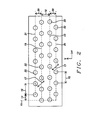
- the distance in the y direction between the centerline 21 of the ball/pad regions 22 in the top row and the centerline 19 of the ball/pad regions 22 in the next row and between the centerline 25 of the ball pad regions 22 bottom row and the centerline 23 of the ball/pad regions in the next to last row is a pitch of a second distance 20.
- the distance between the centerlines 19 and 23 of the ball/pad regions in the two middle rows is a pitch of a third distance 18.
- the distance between the ball/pad regions in the first row and the nearest neighbor ball/pad regions in the second row and between the ball/pad regions in the last row and the nearest neighbor ball/pad regions in the next to last row is a pitch of a fourth distance 17
- the first distance 16 is about 0.5mm
- the second distance 20 is about 0.32mm
- the third distance 18 is about 0.4mm.
- different values for the first, second, and third distances could be used which would result in a different fourth distance.
- the location of the left most ball/pad regions are on a reference line 15.
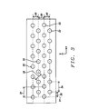
- Fig. 3 shows a top view of a printed circuit board of this invention showing four rows of an x-y grid for locating the ball/pad regions 22.
- the ball/pad regions 22 have a first pitch in the x direction of a first distance 24 for all four rows.
- the second row and bottom row have an off-set in the x direction of a second distance 33, which is one half of the first distance 24.
- the pitch of the centerlines of the ball/pad regions in the y direction have a second pitch of a second distance 30. This results in a separation between nearest neighbor ball/pad regions of a third distance 28.
- a first distance 24 of about 0.5 mm and a second distance 30 of about 0.32 mm results in a third distance 28 of about 0.41 mm.
- the location of the left most ball/pad regions are on a reference line 31.
- first distance 24 and second distance 30 can be used, which will provide a different third distance 28 for separation between nearest neighbor ball/pad regions.
- first distance 24 of 0.58 mm and a second distance 30 of 0.29 mm results in a third distance 28 of about 0.41 mm.
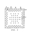
- Fig. 4 shows another embodiment of the ball/pad region layout of this invention.
- Fig. 4 shows a top view of a printed circuit board 37 having a ball/pad region layout as described in a previous paragraph and shown in Fig. 3 around the four edges of the printed circuit board.
- like reference numbers identify like features of the invention as described above and shown in Fig. 3 .
- Fig. 4 also shows ball/pad regions 35 on a more widely spaced grid at the center portion of the printed circuit board.
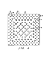
- Fig. 5 shows the printed circuit board of Fig. 4 also showing the placement of standard vias 35.
Abstract
This invention provides layout schemes for ball/pad regions on a printed circuit board for a small regular ball/pad region grid that provides additional space between ball/pad regions for increased wiring capability. The layout scheme is consistent with printed circuit board manufacturing requirements and minimum wiring channel requirements demanded by high density integrated circuit chips.
Description
- This invention relates to a compressed ball/pad region layout grid or matrix for printed circuit boards which will carry integrated circuits and possibly other circuit components. The layout allows spacing for conductors and accommodates high density spacing for integrated circuit pads.
-
U.S. Pat. No. 7,652,379 B2 to Poddar describes a bond pad stack having two conductor layers below a third conductor layer. The third conductor layer has a width that is greater than the width of each of the two conductor layers below the third layer. -
U.S. Pat. No. 7,495,296 B2 to Maeda et al . describes a layout of a multichannel semiconductor integrated circuit having ternary circuits in order to increase the degree of integration. -
U.S. Pat. No. 6,168,854 B1 to Gibbs describes a method of manufacturing printed circuit boards having high density conductive patterns comprising at least one pad suitable for forming a solder connection with at least one surface mounted component. A process is also described which applies a resist to a conductive pattern, etching the conducting pattern, and using the resist to form a conducting coating on the conducting pattern. -
U.S. Pat. No. 6,057,601 to Lau et al. describes a semiconductor ball grid array package for integrated circuits which have input and output counts higher than 250. The package includes a supporting heat spreader layer having a plurality of saw teeth to penetrate an adhesive layer covering a plurality of ground planes. These ground planes are formed on a backside of a substrate supporting a semiconductor device such that the heat spreader can function as a ground terminal for the semiconductor device. -
U.S. Pat. No. 5,818,114 to Pendse et al. describes a radially staggered bonding pad arrangement around the center of a semiconductor die. The bonding pad arrangement allows for increased lead frame density used for wire bonding conductors between the semiconductor circuit pads and the staggered bonding pad arrangement. -
U.S. Pat. No. 5,567,655 to Rostoker et al. describes a bond pad layout on semiconductor circuit chips which reduces thermally induced mechanical stresses. The bond pads are equidistant from the centerline of the chip. Bond pads on either side of the centerline are staggered. - Today's standard IC (integrated circuit) package ball/pad region layout is defined by a regular pitch in the x and y direction, as shown in
Fig. 1. Fig. 1 shows a top view of a standard integratedcircuit board 10 having a number of ball/pad regions 11. Thepitch 12 is the same in the x and y directions and is determined by the number of required ball/pad regions and the target package size. Typically manufacturing rules require a minimum pitch for a given manufacturing technology. As the density of circuits in integrated circuit chips increases and the size of the chips decreases more wiring channels are required. Smaller pitch is a serious limitation to the availability of sufficient wiring channels. - ICs with a single outside row and/or column of balls/pads may be routed on a PCB (printed circuit board) using a single outer layer of metal. To route ICs with a higher number of rows/columns the PCBs typically have to use multiple layers of metal. Inner rows/columns are then routed on the outside layer only towards a close placed via, which then allows a further signal routing inside a deeper PCB layer. Vias are drilled holes with a layer of copper at the circumference. Standard vias are mechanically drilled and have a typical minimum hole diameter of 200-300um. Because of mechanical tolerances the connected landing pads of standard vias are typically ≥ 550um.
- Following the trend for miniaturization and reduced PCB space the ball/pad pitch of ICs with a higher level of integration has been reduced from 0.8mm and 0.65mm towards 0.5mm and 0.4mm with plans to go even towards 0.3mm. This has created some challenges for the signal routing on the PCB. But from 0.5mm pitch standard vias can no longer be placed between balls/pads. For about 0.4mm or smaller ball/pad pitch it is no longer possible to route signals between regular spaced balls/pad regions.
- It is a principal objective of this invention to provide a ball/pad layout scheme that meets manufacturing requirements for a small regular ball/pad region grid and provides additional space between ball/pad regions for increased wiring capability.
- This objective is achieved by using a different x and y ball/pad pitches in local areas of the integrated circuit package. A staggered ball/pad region pitch arrangement is used to achieve a reduced pitch in one direction while maintaining a minimum ball to ball (pad to pad) distance. A ball/pad region pitch of about 0.5 mm can be used in the x direction and a pitch of about 0.32 mm in the y direction with alternating rows locating balls/pads at the gaps of adjacent rows. This provides a spacing of about 0.4mm between nearest balls/pads in adjacent rows. A different ball/pad region pitch can be used in other regions of the integrated circuit package.
-
-
Fig. 1 shows a top view of a printed circuit board having a standard x-y grid of ball/pad regions. -
Fig. 2 shows a top view of a printed circuit board of this invention showing four rows of an x-y ball/pad region grid using a first pitch in the x direction, the top row and bottom row having a one half first pitch off-set in the x direction, a second pitch in the y direction between the top row and the adjacent row and the bottom row and the adjacent row, and a third pitch between the two middle rows. -
Fig. 3 shows a top view of a printed circuit board of this invention showing four rows of an x-y ball/pad region grid having a different pitch in the x and y directions with every second row having a one half pitch offset in the x direction. -
Fig. 4 shows a top view of a printed circuit board of this invention showing a ball/pad region grid of the type shown inFig. 3 at the four edges of the printed circuit board with larger spacing between the ball/pad regions in the center of the board. -
Fig. 5 shows a top view of the printed circuit board shown inFig. 4 showing placement of standard vias in the board. - Refer now to
Fig 2 for a description of a preferred embodiment of the ball/pad region layout of this invention.Fig. 2 shows a top view of a printed circuit board of this invention showing four rows of an x-y grid for locating the ball/pad regions 22. The ball/pad regions 22 have a pitch of afirst distance 16 in the x direction for all four rows and the top row and bottom row have an off-set 14 of one half of thefirst distance 16 in the x direction. The distance in the y direction between thecenterline 21 of the ball/pad regions 22 in the top row and thecenterline 19 of the ball/pad regions 22 in the next row and between thecenterline 25 of theball pad regions 22 bottom row and thecenterline 23 of the ball/pad regions in the next to last row is a pitch of asecond distance 20. The distance between thecenterlines third distance 18. The distance between the ball/pad regions in the first row and the nearest neighbor ball/pad regions in the second row and between the ball/pad regions in the last row and the nearest neighbor ball/pad regions in the next to last row is a pitch of afourth distance 17 In this example thefirst distance 16 is about 0.5mm, thesecond distance 20 is about 0.32mm, and thethird distance 18 is about 0.4mm. This provides afourth distance 17 of about 0.4mm which in this example is about the same as the third distance. Of course, different values for the first, second, and third distances could be used which would result in a different fourth distance. The location of the left most ball/pad regions are on areference line 15. - Refer now to
Fig. 3 for another preferred embodiment of the ball/pad region layout of this invention.Fig. 3 shows a top view of a printed circuit board of this invention showing four rows of an x-y grid for locating the ball/pad regions 22. The ball/pad regions 22 have a first pitch in the x direction of afirst distance 24 for all four rows. The second row and bottom row have an off-set in the x direction of asecond distance 33, which is one half of thefirst distance 24. The pitch of the centerlines of the ball/pad regions in the y direction have a second pitch of asecond distance 30. This results in a separation between nearest neighbor ball/pad regions of athird distance 28. As an example afirst distance 24 of about 0.5 mm and asecond distance 30 of about 0.32 mm results in athird distance 28 of about 0.41 mm. The location of the left most ball/pad regions are on areference line 31. - Those skilled in the art will readily recognize that different values for the
first distance 24 andsecond distance 30 can be used, which will provide a differentthird distance 28 for separation between nearest neighbor ball/pad regions. For example afirst distance 24 of 0.58 mm and asecond distance 30 of 0.29 mm results in athird distance 28 of about 0.41 mm. -
Fig. 4 shows another embodiment of the ball/pad region layout of this invention.Fig. 4 shows a top view of a printed circuit board 37 having a ball/pad region layout as described in a previous paragraph and shown inFig. 3 around the four edges of the printed circuit board. In the regions around the four edges of the printed circuit board like reference numbers identify like features of the invention as described above and shown inFig. 3 .Fig. 4 also shows ball/pad regions 35 on a more widely spaced grid at the center portion of the printed circuit board.Fig. 5 shows the printed circuit board ofFig. 4 also showing the placement ofstandard vias 35. - While the invention has been particularly shown and described with reference to the preferred embodiments thereof, it will be understood by those skilled in the art that various changes in form and details may be made without departing from the spirit and scope of the invention.
Claims (12)
- A ball/pad region layout pattern, comprising:- a circuit board for supporting circuit components and conductive circuit patterns, wherein said circuit board has a plurality of ball/pad regions;- an x-y grid for location of said ball/pad regions, wherein said x and y directions are perpendicular;- a reference line parallel to said y direction;- one or more first rows of conductive ball/pad regions formed on said circuit board wherein the centers of said ball/pad regions in said first rows are on a straight line parallel to said x direction, each said ball/pad region has a center, said centers of each of said ball/pad regions in each of said first rows are located one half of a first distance plus N multiplied by said first distance from said reference line, and wherein N is zero or a positive integer of one or greater; and- one or more second rows of conductive ball/pad regions formed on said circuit board wherein the centers of said ball/pad regions in said second rows are on a straight line parallel to said x direction, each said ball/pad region has a center, said centers of each of said ball/pad regions in each of said second rows are located M multiplied said first distance from said reference line, M is zero or a positive integer of one or greater, and wherein each said first row is adjacent to and a second distance from one of said second rows and each said second row is adjacent to and said second distance from one of said first rows and adjacent to and a third distance from one of said second rows.
- The ball/pad region layout of claim 1 wherein said third distance is about 0.4 millimeters.
- A ball/pad region layout pattern, comprising:- a circuit board for supporting circuit components and conductive circuit patterns, wherein said circuit board has a plurality of ball/pad regions;- an x-y grid for location of said ball/pad regions, wherein said x and y directions are perpendicular;- a reference line parallel to said y direction;- one or more first rows of conductive ball/pad regions formed on said circuit board wherein the centers of said ball/pad regions in said first rows are on a straight line parallel to said x direction, each said ball/pad region has a center, said centers of each of said ball/pad regions in each of said first rows are located N multiplied by a first distance from said reference line, and wherein N is positive integer of zero, one, or greater; and- one or more second rows of conductive ball/pad regions formed on said circuit board wherein the centers of said ball/pad regions in said second rows are on a straight line parallel to said x direction, each said ball/pad region has a center, said centers of each of said ball/pad regions in each of said second rows are located one half of said first distance plus M multiplied by said first distance from said reference line, wherein M is a positive integer of zero, one, or greater, and wherein each said first row is adjacent to and a second distance from at one or two of said second rows and each said second row is adjacent to and said second distance from one or two of said first rows.
- The ball/pad region layout of claim 1 or 3 wherein said circuit components comprise integrated circuit devices.
- The ball/pad region layout of claim 1 or 3 wherein said ball/pad regions are circular.
- The ball/pad region layout of claim 1 or 3 wherein said first distance is about 0.5 millimeters.
- The ball/pad region layout of claim 1 or 3 wherein said second distance is about 0.32 millimeters.
- The ball/pad region layout of claim 1 or 33 wherein said first distance is about 0.58 millimeters and said second distance is about 0.29mm.
- The ball/pad region layout of claim 1 or 3 wherein there are two said first rows and two said second rows and said first and second rows are arranged consecutively in said y direction as one of said first rows, one of said second rows, one of said first rows, and one of said second rows.
- The ball/pad region layout of claim 1 or 3 wherein said circuit board may have different regions with different said ball/pad layouts.
- The ball/pad region layout of claim 1 or 3 wherein said circuit board is a printed circuit board.
- The ball/pad region layout of claim 1 or 3 wherein said circuit board also has vias.
Priority Applications (2)
| Application Number | Priority Date | Filing Date | Title |
|---|---|---|---|
| EP11368010A EP2503594A1 (en) | 2011-03-21 | 2011-03-21 | Signal routing optimized IC package ball/pad layout |
| US13/066,656 US20120241208A1 (en) | 2011-03-21 | 2011-04-20 | Signal routing Optimized IC package ball/pad layout |
Applications Claiming Priority (1)
| Application Number | Priority Date | Filing Date | Title |
|---|---|---|---|
| EP11368010A EP2503594A1 (en) | 2011-03-21 | 2011-03-21 | Signal routing optimized IC package ball/pad layout |
Publications (1)
| Publication Number | Publication Date |
|---|---|
| EP2503594A1 true EP2503594A1 (en) | 2012-09-26 |
Family
ID=44118475
Family Applications (1)
| Application Number | Title | Priority Date | Filing Date |
|---|---|---|---|
| EP11368010A Withdrawn EP2503594A1 (en) | 2011-03-21 | 2011-03-21 | Signal routing optimized IC package ball/pad layout |
Country Status (2)
| Country | Link |
|---|---|
| US (1) | US20120241208A1 (en) |
| EP (1) | EP2503594A1 (en) |
Families Citing this family (9)
| Publication number | Priority date | Publication date | Assignee | Title |
|---|---|---|---|---|
| US8988895B2 (en) * | 2011-08-23 | 2015-03-24 | Tessera, Inc. | Interconnection elements with encased interconnects |
| JP2015088539A (en) * | 2013-10-29 | 2015-05-07 | 株式会社デンソー | Semiconductor package and wiring board mounting the same |
| US10177107B2 (en) * | 2016-08-01 | 2019-01-08 | Xilinx, Inc. | Heterogeneous ball pattern package |
| JP6826185B2 (en) * | 2017-02-22 | 2021-02-03 | 京セラ株式会社 | Wiring boards, electronics and electronic modules |
| DE102017218273B4 (en) * | 2017-10-12 | 2022-05-12 | Vitesco Technologies GmbH | semiconductor assembly |
| DE102017128568A1 (en) * | 2017-12-01 | 2019-06-06 | Infineon Technologies Ag | SEMICONDUCTOR CHIP WITH A VARIETY OF EXTERNAL CONTACTS, CHIP ARRANGEMENT AND METHOD FOR CHECKING AN ORIENTATION OF A POSITION OF A SEMICONDUCTOR CHIP |
| WO2020043170A1 (en) * | 2018-08-31 | 2020-03-05 | Changxin Memory Technologies, Inc. | Arrangement of bond pads on an integrated circuit chip |
| CN109618489A (en) * | 2018-12-29 | 2019-04-12 | 晶晨半导体(深圳)有限公司 | Printed circuit board |
| US11705378B2 (en) * | 2020-07-20 | 2023-07-18 | Taiwan Semiconductor Manufacturing Company, Ltd. | Semiconductor packages and methods of forming the same |
Citations (12)
| Publication number | Priority date | Publication date | Assignee | Title |
|---|---|---|---|---|
| US5567655A (en) | 1993-05-05 | 1996-10-22 | Lsi Logic Corporation | Method for forming interior bond pads having zig-zag linear arrangement |
| US5818114A (en) | 1995-05-26 | 1998-10-06 | Hewlett-Packard Company | Radially staggered bond pad arrangements for integrated circuit pad circuitry |
| US6057601A (en) | 1998-11-27 | 2000-05-02 | Express Packaging Systems, Inc. | Heat spreader with a placement recess and bottom saw-teeth for connection to ground planes on a thin two-sided single-core BGA substrate |
| US6168854B1 (en) | 1996-12-23 | 2001-01-02 | Nortel Networks Limited | Method of making a printed circuit board having a tin/lead coating |
| US6407462B1 (en) * | 2000-12-30 | 2002-06-18 | Lsi Logic Corporation | Irregular grid bond pad layout arrangement for a flip chip package |
| WO2003065451A1 (en) * | 2002-01-31 | 2003-08-07 | Thomson Licensing S.A. | Flip chip die bond pads, die bond pad placement and routing optimization |
| US6664483B2 (en) * | 2001-05-15 | 2003-12-16 | Intel Corporation | Electronic package with high density interconnect and associated methods |
| US6734545B1 (en) * | 1995-11-29 | 2004-05-11 | Hitachi, Ltd. | BGA type semiconductor device and electronic equipment using the same |
| US20050186769A1 (en) * | 2004-02-24 | 2005-08-25 | Young Dave W. | Hexagonal array structure for ball grid array packages |
| US7495296B2 (en) | 2004-06-01 | 2009-02-24 | Panasonic Corporation | Semiconductor integrated circuit device |
| US20090189158A1 (en) * | 2008-01-30 | 2009-07-30 | Kabushiki Kaisha Toshiba | Semiconductor device |
| US7652379B2 (en) | 2007-07-23 | 2010-01-26 | National Semiconductor Corporation | Bond pad stacks for ESD under pad and active under pad bonding |
Family Cites Families (10)
| Publication number | Priority date | Publication date | Assignee | Title |
|---|---|---|---|---|
| US6111756A (en) * | 1998-09-11 | 2000-08-29 | Fujitsu Limited | Universal multichip interconnect systems |
| US6815621B2 (en) * | 2000-10-02 | 2004-11-09 | Samsung Electronics Co., Ltd. | Chip scale package, printed circuit board, and method of designing a printed circuit board |
| US6556454B1 (en) * | 2000-10-31 | 2003-04-29 | Agilent Technologies, Inc. | High density contact arrangement |
| JP3785083B2 (en) * | 2001-11-07 | 2006-06-14 | 株式会社東芝 | Semiconductor device, electronic card and pad rearrangement substrate |
| US6768206B2 (en) * | 2002-05-07 | 2004-07-27 | Kabushiki Kaisha Toshiba | Organic substrate for flip chip bonding |
| US6919635B2 (en) * | 2003-11-04 | 2005-07-19 | International Business Machines Corporation | High density microvia substrate with high wireability |
| US7372169B2 (en) * | 2005-10-11 | 2008-05-13 | Via Technologies, Inc. | Arrangement of conductive pads on grid array package and on circuit board |
| JP5352146B2 (en) * | 2008-07-23 | 2013-11-27 | ルネサスエレクトロニクス株式会社 | Semiconductor device |
| US9355951B2 (en) * | 2009-08-28 | 2016-05-31 | Marvell World Trade Ltd. | Interconnect layouts for electronic assemblies |
| JP5342422B2 (en) * | 2009-12-10 | 2013-11-13 | ルネサスエレクトロニクス株式会社 | Semiconductor device and manufacturing method thereof |
-
2011
- 2011-03-21 EP EP11368010A patent/EP2503594A1/en not_active Withdrawn
- 2011-04-20 US US13/066,656 patent/US20120241208A1/en not_active Abandoned
Patent Citations (12)
| Publication number | Priority date | Publication date | Assignee | Title |
|---|---|---|---|---|
| US5567655A (en) | 1993-05-05 | 1996-10-22 | Lsi Logic Corporation | Method for forming interior bond pads having zig-zag linear arrangement |
| US5818114A (en) | 1995-05-26 | 1998-10-06 | Hewlett-Packard Company | Radially staggered bond pad arrangements for integrated circuit pad circuitry |
| US6734545B1 (en) * | 1995-11-29 | 2004-05-11 | Hitachi, Ltd. | BGA type semiconductor device and electronic equipment using the same |
| US6168854B1 (en) | 1996-12-23 | 2001-01-02 | Nortel Networks Limited | Method of making a printed circuit board having a tin/lead coating |
| US6057601A (en) | 1998-11-27 | 2000-05-02 | Express Packaging Systems, Inc. | Heat spreader with a placement recess and bottom saw-teeth for connection to ground planes on a thin two-sided single-core BGA substrate |
| US6407462B1 (en) * | 2000-12-30 | 2002-06-18 | Lsi Logic Corporation | Irregular grid bond pad layout arrangement for a flip chip package |
| US6664483B2 (en) * | 2001-05-15 | 2003-12-16 | Intel Corporation | Electronic package with high density interconnect and associated methods |
| WO2003065451A1 (en) * | 2002-01-31 | 2003-08-07 | Thomson Licensing S.A. | Flip chip die bond pads, die bond pad placement and routing optimization |
| US20050186769A1 (en) * | 2004-02-24 | 2005-08-25 | Young Dave W. | Hexagonal array structure for ball grid array packages |
| US7495296B2 (en) | 2004-06-01 | 2009-02-24 | Panasonic Corporation | Semiconductor integrated circuit device |
| US7652379B2 (en) | 2007-07-23 | 2010-01-26 | National Semiconductor Corporation | Bond pad stacks for ESD under pad and active under pad bonding |
| US20090189158A1 (en) * | 2008-01-30 | 2009-07-30 | Kabushiki Kaisha Toshiba | Semiconductor device |
Also Published As
| Publication number | Publication date |
|---|---|
| US20120241208A1 (en) | 2012-09-27 |
Similar Documents
| Publication | Publication Date | Title |
|---|---|---|
| EP2503594A1 (en) | Signal routing optimized IC package ball/pad layout | |
| KR101218011B1 (en) | Flip chip interconnect pad layout semiconductor package and its production method | |
| EP1705967B1 (en) | Off-grid decoupling capacitor of ball grid array (BGA) devices and method | |
| JP2003007750A (en) | Semiconductor device | |
| JP2003188508A (en) | Printed circuit board, surface-mount circuit component, and circuit module | |
| US11369020B2 (en) | Stacked transmission line | |
| EP1753274A2 (en) | Alternating micro-vias and through-hole vias for a BGA interconnect grid in order to create improved PCB routing channels | |
| KR100967565B1 (en) | Semiconductor component | |
| US6664620B2 (en) | Integrated circuit die and/or package having a variable pitch contact array for maximization of number of signal lines per routing layer | |
| JP3730625B2 (en) | Organic substrate for flip chip bonding | |
| EP1714530B1 (en) | Method for increasing a routing density for a circuit board and such a circuit board | |
| US7161812B1 (en) | System for arraying surface mount grid array contact pads to optimize trace escape routing for a printed circuit board | |
| US20090065935A1 (en) | Systems and methods for ball grid array (bga) escape routing | |
| JP2005166794A (en) | Component package, printed wiring board and electronic apparatus | |
| US20090174072A1 (en) | Semiconductor system having bga package with radially ball-depopulated substrate zones and board with radial via zones | |
| CN109509737B (en) | Electronic packaging component and circuit layout structure | |
| JP2008078646A (en) | Printed circuit board for package, and manufacturing method thereof | |
| JP3994312B2 (en) | Printed wiring board, manufacturing method thereof, and interposer substrate | |
| US8013253B2 (en) | Electrical connection board and assembly of such a board and a semiconductor component comprising an integrated circuit chip | |
| US20070114578A1 (en) | Layout structure of ball grid array | |
| JP3008887U (en) | IC pitch conversion board | |
| JP2009164294A (en) | Multilayer circuit board, and semiconductor device | |
| WO2002067325A2 (en) | High-density flip-chip interconnect | |
| JP2005228776A (en) | Wiring method and wiring board | |
| JP2005005601A (en) | Wiring layout structure for printed circuit wiring board |
Legal Events
| Date | Code | Title | Description |
|---|---|---|---|
| PUAI | Public reference made under article 153(3) epc to a published international application that has entered the european phase |
Free format text: ORIGINAL CODE: 0009012 |
|
| AK | Designated contracting states |
Kind code of ref document: A1 Designated state(s): AL AT BE BG CH CY CZ DE DK EE ES FI FR GB GR HR HU IE IS IT LI LT LU LV MC MK MT NL NO PL PT RO RS SE SI SK SM TR |
|
| AX | Request for extension of the european patent |
Extension state: BA ME |
|
| 17P | Request for examination filed |
Effective date: 20130326 |
|
| 17Q | First examination report despatched |
Effective date: 20140214 |
|
| STAA | Information on the status of an ep patent application or granted ep patent |
Free format text: STATUS: THE APPLICATION IS DEEMED TO BE WITHDRAWN |
|
| 18D | Application deemed to be withdrawn |
Effective date: 20161001 |