EP2478564B1 - Crystalline solar cell and method for producing said type of solar cell - Google Patents
Crystalline solar cell and method for producing said type of solar cell Download PDFInfo
- Publication number
- EP2478564B1 EP2478564B1 EP10754749.9A EP10754749A EP2478564B1 EP 2478564 B1 EP2478564 B1 EP 2478564B1 EP 10754749 A EP10754749 A EP 10754749A EP 2478564 B1 EP2478564 B1 EP 2478564B1
- Authority
- EP
- European Patent Office
- Prior art keywords
- layer
- solar cell
- doped
- sin
- sio
- Prior art date
- Legal status (The legal status is an assumption and is not a legal conclusion. Google has not performed a legal analysis and makes no representation as to the accuracy of the status listed.)
- Active
Links
- 238000004519 manufacturing process Methods 0.000 title claims description 12
- 239000000758 substrate Substances 0.000 claims description 15
- VYPSYNLAJGMNEJ-UHFFFAOYSA-N Silicium dioxide Chemical compound O=[Si]=O VYPSYNLAJGMNEJ-UHFFFAOYSA-N 0.000 claims description 14
- 239000002800 charge carrier Substances 0.000 claims description 14
- 239000000463 material Substances 0.000 claims description 14
- 229910052760 oxygen Inorganic materials 0.000 claims description 11
- 238000000034 method Methods 0.000 claims description 9
- 229910021417 amorphous silicon Inorganic materials 0.000 claims description 8
- 229910052814 silicon oxide Inorganic materials 0.000 claims description 8
- 229910052782 aluminium Inorganic materials 0.000 claims description 7
- 229910052787 antimony Inorganic materials 0.000 claims description 7
- 229910052796 boron Inorganic materials 0.000 claims description 7
- 229910052804 chromium Inorganic materials 0.000 claims description 7
- 229910052802 copper Inorganic materials 0.000 claims description 7
- 229910052733 gallium Inorganic materials 0.000 claims description 7
- 229910052738 indium Inorganic materials 0.000 claims description 7
- 229910052742 iron Inorganic materials 0.000 claims description 7
- 229910052757 nitrogen Inorganic materials 0.000 claims description 7
- 229910052698 phosphorus Inorganic materials 0.000 claims description 7
- 229910052716 thallium Inorganic materials 0.000 claims description 7
- 229910052721 tungsten Inorganic materials 0.000 claims description 7
- 229910052720 vanadium Inorganic materials 0.000 claims description 7
- XLOMVQKBTHCTTD-UHFFFAOYSA-N Zinc monoxide Chemical compound [Zn]=O XLOMVQKBTHCTTD-UHFFFAOYSA-N 0.000 claims description 6
- QVGXLLKOCUKJST-UHFFFAOYSA-N atomic oxygen Chemical compound [O] QVGXLLKOCUKJST-UHFFFAOYSA-N 0.000 claims description 4
- 239000007788 liquid Substances 0.000 claims description 4
- 239000001301 oxygen Substances 0.000 claims description 4
- 229910020286 SiOxNy Inorganic materials 0.000 claims description 3
- 230000015572 biosynthetic process Effects 0.000 claims description 3
- AMGQUBHHOARCQH-UHFFFAOYSA-N indium;oxotin Chemical compound [In].[Sn]=O AMGQUBHHOARCQH-UHFFFAOYSA-N 0.000 claims description 3
- 238000009413 insulation Methods 0.000 claims description 3
- 239000011787 zinc oxide Substances 0.000 claims description 3
- UMVBXBACMIOFDO-UHFFFAOYSA-N [N].[Si] Chemical compound [N].[Si] UMVBXBACMIOFDO-UHFFFAOYSA-N 0.000 claims description 2
- -1 Al2Ox Inorganic materials 0.000 claims 2
- CBENFWSGALASAD-UHFFFAOYSA-N Ozone Chemical compound [O-][O+]=O CBENFWSGALASAD-UHFFFAOYSA-N 0.000 claims 2
- 229910003087 TiOx Inorganic materials 0.000 claims 2
- HLLICFJUWSZHRJ-UHFFFAOYSA-N tioxidazole Chemical compound CCCOC1=CC=C2N=C(NC(=O)OC)SC2=C1 HLLICFJUWSZHRJ-UHFFFAOYSA-N 0.000 claims 2
- 230000008021 deposition Effects 0.000 claims 1
- 125000004435 hydrogen atom Chemical group [H]* 0.000 claims 1
- 229910052581 Si3N4 Inorganic materials 0.000 description 27
- HQVNEWCFYHHQES-UHFFFAOYSA-N silicon nitride Chemical compound N12[Si]34N5[Si]62N3[Si]51N64 HQVNEWCFYHHQES-UHFFFAOYSA-N 0.000 description 27
- LIVNPJMFVYWSIS-UHFFFAOYSA-N silicon monoxide Chemical compound [Si-]#[O+] LIVNPJMFVYWSIS-UHFFFAOYSA-N 0.000 description 25
- 230000015556 catabolic process Effects 0.000 description 23
- 238000006731 degradation reaction Methods 0.000 description 23
- XUIMIQQOPSSXEZ-UHFFFAOYSA-N Silicon Chemical compound [Si] XUIMIQQOPSSXEZ-UHFFFAOYSA-N 0.000 description 19
- 229910052710 silicon Inorganic materials 0.000 description 19
- 239000010703 silicon Substances 0.000 description 19
- 229910052751 metal Inorganic materials 0.000 description 9
- 239000002184 metal Substances 0.000 description 9
- 230000008929 regeneration Effects 0.000 description 9
- 238000011069 regeneration method Methods 0.000 description 9
- 239000012535 impurity Substances 0.000 description 7
- 239000011248 coating agent Substances 0.000 description 5
- 238000000576 coating method Methods 0.000 description 5
- 230000000694 effects Effects 0.000 description 5
- 239000005038 ethylene vinyl acetate Substances 0.000 description 5
- 238000005286 illumination Methods 0.000 description 5
- 238000005215 recombination Methods 0.000 description 5
- 230000006798 recombination Effects 0.000 description 5
- 238000003860 storage Methods 0.000 description 5
- DQXBYHZEEUGOBF-UHFFFAOYSA-N but-3-enoic acid;ethene Chemical compound C=C.OC(=O)CC=C DQXBYHZEEUGOBF-UHFFFAOYSA-N 0.000 description 4
- 229910021419 crystalline silicon Inorganic materials 0.000 description 4
- 238000002161 passivation Methods 0.000 description 4
- 229920003023 plastic Polymers 0.000 description 4
- 229920001200 poly(ethylene-vinyl acetate) Polymers 0.000 description 4
- 238000009825 accumulation Methods 0.000 description 3
- 230000005684 electric field Effects 0.000 description 3
- 238000011049 filling Methods 0.000 description 3
- 239000011888 foil Substances 0.000 description 3
- 239000011521 glass Substances 0.000 description 3
- 239000004033 plastic Substances 0.000 description 3
- 230000010287 polarization Effects 0.000 description 3
- 230000009467 reduction Effects 0.000 description 3
- 230000002441 reversible effect Effects 0.000 description 3
- 239000000377 silicon dioxide Substances 0.000 description 3
- 230000007423 decrease Effects 0.000 description 2
- 239000002019 doping agent Substances 0.000 description 2
- 230000001771 impaired effect Effects 0.000 description 2
- 239000002985 plastic film Substances 0.000 description 2
- 229920006255 plastic film Polymers 0.000 description 2
- 229920002620 polyvinyl fluoride Polymers 0.000 description 2
- 230000008569 process Effects 0.000 description 2
- 230000000750 progressive effect Effects 0.000 description 2
- 235000012239 silicon dioxide Nutrition 0.000 description 2
- 229910018557 Si O Inorganic materials 0.000 description 1
- 230000009471 action Effects 0.000 description 1
- 230000003667 anti-reflective effect Effects 0.000 description 1
- 239000000969 carrier Substances 0.000 description 1
- 230000003197 catalytic effect Effects 0.000 description 1
- 238000006243 chemical reaction Methods 0.000 description 1
- 238000010276 construction Methods 0.000 description 1
- 238000006073 displacement reaction Methods 0.000 description 1
- 230000003993 interaction Effects 0.000 description 1
- 238000003475 lamination Methods 0.000 description 1
- 238000011068 loading method Methods 0.000 description 1
- 238000005259 measurement Methods 0.000 description 1
- 238000001465 metallisation Methods 0.000 description 1
- 150000004767 nitrides Chemical class 0.000 description 1
- 230000002123 temporal effect Effects 0.000 description 1
- 238000010023 transfer printing Methods 0.000 description 1
Images

Classifications
-
- H—ELECTRICITY
- H01—ELECTRIC ELEMENTS
- H01L—SEMICONDUCTOR DEVICES NOT COVERED BY CLASS H10
- H01L31/00—Semiconductor devices sensitive to infrared radiation, light, electromagnetic radiation of shorter wavelength or corpuscular radiation and specially adapted either for the conversion of the energy of such radiation into electrical energy or for the control of electrical energy by such radiation; Processes or apparatus specially adapted for the manufacture or treatment thereof or of parts thereof; Details thereof
- H01L31/04—Semiconductor devices sensitive to infrared radiation, light, electromagnetic radiation of shorter wavelength or corpuscular radiation and specially adapted either for the conversion of the energy of such radiation into electrical energy or for the control of electrical energy by such radiation; Processes or apparatus specially adapted for the manufacture or treatment thereof or of parts thereof; Details thereof adapted as photovoltaic [PV] conversion devices
-
- H—ELECTRICITY
- H01—ELECTRIC ELEMENTS
- H01L—SEMICONDUCTOR DEVICES NOT COVERED BY CLASS H10
- H01L31/00—Semiconductor devices sensitive to infrared radiation, light, electromagnetic radiation of shorter wavelength or corpuscular radiation and specially adapted either for the conversion of the energy of such radiation into electrical energy or for the control of electrical energy by such radiation; Processes or apparatus specially adapted for the manufacture or treatment thereof or of parts thereof; Details thereof
- H01L31/02—Details
- H01L31/02016—Circuit arrangements of general character for the devices
- H01L31/02019—Circuit arrangements of general character for the devices for devices characterised by at least one potential jump barrier or surface barrier
- H01L31/02021—Circuit arrangements of general character for the devices for devices characterised by at least one potential jump barrier or surface barrier for solar cells
-
- H—ELECTRICITY
- H01—ELECTRIC ELEMENTS
- H01L—SEMICONDUCTOR DEVICES NOT COVERED BY CLASS H10
- H01L31/00—Semiconductor devices sensitive to infrared radiation, light, electromagnetic radiation of shorter wavelength or corpuscular radiation and specially adapted either for the conversion of the energy of such radiation into electrical energy or for the control of electrical energy by such radiation; Processes or apparatus specially adapted for the manufacture or treatment thereof or of parts thereof; Details thereof
- H01L31/02—Details
- H01L31/0216—Coatings
- H01L31/02161—Coatings for devices characterised by at least one potential jump barrier or surface barrier
- H01L31/02167—Coatings for devices characterised by at least one potential jump barrier or surface barrier for solar cells
- H01L31/02168—Coatings for devices characterised by at least one potential jump barrier or surface barrier for solar cells the coatings being antireflective or having enhancing optical properties for the solar cells
-
- H—ELECTRICITY
- H01—ELECTRIC ELEMENTS
- H01L—SEMICONDUCTOR DEVICES NOT COVERED BY CLASS H10
- H01L31/00—Semiconductor devices sensitive to infrared radiation, light, electromagnetic radiation of shorter wavelength or corpuscular radiation and specially adapted either for the conversion of the energy of such radiation into electrical energy or for the control of electrical energy by such radiation; Processes or apparatus specially adapted for the manufacture or treatment thereof or of parts thereof; Details thereof
- H01L31/02—Details
- H01L31/0224—Electrodes
- H01L31/022466—Electrodes made of transparent conductive layers, e.g. TCO, ITO layers
-
- H—ELECTRICITY
- H01—ELECTRIC ELEMENTS
- H01L—SEMICONDUCTOR DEVICES NOT COVERED BY CLASS H10
- H01L31/00—Semiconductor devices sensitive to infrared radiation, light, electromagnetic radiation of shorter wavelength or corpuscular radiation and specially adapted either for the conversion of the energy of such radiation into electrical energy or for the control of electrical energy by such radiation; Processes or apparatus specially adapted for the manufacture or treatment thereof or of parts thereof; Details thereof
- H01L31/04—Semiconductor devices sensitive to infrared radiation, light, electromagnetic radiation of shorter wavelength or corpuscular radiation and specially adapted either for the conversion of the energy of such radiation into electrical energy or for the control of electrical energy by such radiation; Processes or apparatus specially adapted for the manufacture or treatment thereof or of parts thereof; Details thereof adapted as photovoltaic [PV] conversion devices
- H01L31/042—PV modules or arrays of single PV cells
- H01L31/048—Encapsulation of modules
-
- H—ELECTRICITY
- H01—ELECTRIC ELEMENTS
- H01L—SEMICONDUCTOR DEVICES NOT COVERED BY CLASS H10
- H01L31/00—Semiconductor devices sensitive to infrared radiation, light, electromagnetic radiation of shorter wavelength or corpuscular radiation and specially adapted either for the conversion of the energy of such radiation into electrical energy or for the control of electrical energy by such radiation; Processes or apparatus specially adapted for the manufacture or treatment thereof or of parts thereof; Details thereof
- H01L31/04—Semiconductor devices sensitive to infrared radiation, light, electromagnetic radiation of shorter wavelength or corpuscular radiation and specially adapted either for the conversion of the energy of such radiation into electrical energy or for the control of electrical energy by such radiation; Processes or apparatus specially adapted for the manufacture or treatment thereof or of parts thereof; Details thereof adapted as photovoltaic [PV] conversion devices
- H01L31/06—Semiconductor devices sensitive to infrared radiation, light, electromagnetic radiation of shorter wavelength or corpuscular radiation and specially adapted either for the conversion of the energy of such radiation into electrical energy or for the control of electrical energy by such radiation; Processes or apparatus specially adapted for the manufacture or treatment thereof or of parts thereof; Details thereof adapted as photovoltaic [PV] conversion devices characterised by at least one potential-jump barrier or surface barrier
- H01L31/068—Semiconductor devices sensitive to infrared radiation, light, electromagnetic radiation of shorter wavelength or corpuscular radiation and specially adapted either for the conversion of the energy of such radiation into electrical energy or for the control of electrical energy by such radiation; Processes or apparatus specially adapted for the manufacture or treatment thereof or of parts thereof; Details thereof adapted as photovoltaic [PV] conversion devices characterised by at least one potential-jump barrier or surface barrier the potential barriers being only of the PN homojunction type, e.g. bulk silicon PN homojunction solar cells or thin film polycrystalline silicon PN homojunction solar cells
-
- H—ELECTRICITY
- H01—ELECTRIC ELEMENTS
- H01L—SEMICONDUCTOR DEVICES NOT COVERED BY CLASS H10
- H01L31/00—Semiconductor devices sensitive to infrared radiation, light, electromagnetic radiation of shorter wavelength or corpuscular radiation and specially adapted either for the conversion of the energy of such radiation into electrical energy or for the control of electrical energy by such radiation; Processes or apparatus specially adapted for the manufacture or treatment thereof or of parts thereof; Details thereof
- H01L31/18—Processes or apparatus specially adapted for the manufacture or treatment of these devices or of parts thereof
-
- Y—GENERAL TAGGING OF NEW TECHNOLOGICAL DEVELOPMENTS; GENERAL TAGGING OF CROSS-SECTIONAL TECHNOLOGIES SPANNING OVER SEVERAL SECTIONS OF THE IPC; TECHNICAL SUBJECTS COVERED BY FORMER USPC CROSS-REFERENCE ART COLLECTIONS [XRACs] AND DIGESTS
- Y02—TECHNOLOGIES OR APPLICATIONS FOR MITIGATION OR ADAPTATION AGAINST CLIMATE CHANGE
- Y02E—REDUCTION OF GREENHOUSE GAS [GHG] EMISSIONS, RELATED TO ENERGY GENERATION, TRANSMISSION OR DISTRIBUTION
- Y02E10/00—Energy generation through renewable energy sources
- Y02E10/50—Photovoltaic [PV] energy
- Y02E10/547—Monocrystalline silicon PV cells
Definitions
- the invention relates to a crystalline solar cell with a p-type doped substrate and a front n-doped region and a back p-doped region, a front side contact, a rear contact and at least one front side first layer of SiN or SiN containing such as Antireflexiohstik.
- the invention also relates to a method for producing a crystalline solar cell with p-type doped substrate and a front-side n-doped region, rear p-doped region, front and back contacts and at least one front layer of SiN or SiN containing as a first layer such as antireflection coating.
- n- and p-doped regions in a pn diode create a space charge zone in which electrons migrate from the n-layer into the p-layer and holes of the p-layer into the n-layer.
- a voltage is applied to the metallic electrodes located on the n- and p-doped layers, a high current flows when the Voltage at the negative electrode is negative. In reverse polarity flows a much lower current.
- Si pn diodes are solar cells or photodetectors, in which a part of the front side is provided with an at least partially transparent layer, which usually has a reflection-reducing effect. Through this layer, light penetrates into the silicon, which is partially absorbed there. Excessive electrons and holes are released. The excess electrons travel in the electric field of the space charge zone from the p-doped to the n-doped region and finally to the metal contacts on the n-doped region, the excess holes migrate from the n-doped to the p-doped region and finally to the metal kinetics on the p -doped area. When a load is placed between the positive and negative electrodes, a current flows.
- modules with double-sided contacted silicon solar cells with p-base doping and n-doped front side have low parallel resistances and thus also low filling factors after the action of high negative system voltages. This is a sign of an emitter-base interaction, and thus is fundamentally different from the effects on surface recombination rate described above. By treatment at elevated temperature and high humidity, the degraded modules partially recover their performance back.
- a solar cell which consists of an n-doped front region and a p-doped back region, a front side photon, a rear contact and at least a first front layer which consist of silicon dioxide and can serve as an antireflection layer.
- the layer may also contain nitrides.
- a backside contact solar cell that has a n-type fundamental doping.
- a region of the solar cell module is biased.
- WO-A-2008/072828 is a solar cell with pn junction, a front-side first SiN layer and a second layer of SiOxNy: Hz refer.
- a solar cell module in which a storage of positive charge carriers in the antireflection layer and a concomitant degradation of the filling factor is thereby avoided by either an external voltage between the solar cell and ground is applied overnight by the antireflection layer is coated on the surface transparent conductive.
- a solar cell with n-based substrate refer to the front of a passivation layer, an n-doped layer and then an anti-reflection layer are applied.
- Subject of the EP 1 304 748 A2 is the production of a solar cell in which catalytic dopants are incorporated into the passivation or antireflection coating for surface or volume passivation.
- the US 2009/0151582 A1 refers to a solar cell with heterojunction.
- the present invention is based on the object, a crystalline solar cell, a method for producing such and a method for producing a solar cell module of the initially described types so that the degradation of the parallel resistance and thus the fill factor is reduced, in particular contacted on both sides of the silicon solar cells with p-base doping, n-doped front and an antireflective layer consisting of silicon nitride due to high negative system voltages or positive charges on the front side.
- the invention provides essentially a crystalline solar cell before, which is characterized in that between the first layer and the n-doped region of a second layer of at least one material from the group of SiN, SiO x, Al 2 O x, SiO x N y : Hz, a-Si: H, TiO x or such material containing and doped to form impurities.
- the SiN-containing or SiN-containing second layer should contain a silicon-nitrogen ratio of 1 to 2.2 and an H atomic concentration of more than 10%.
- positive and / or negative charge carriers are incorporated in the first layer after the first layer has been produced.
- the surface charge density of the charge carriers is preferably> 1 ⁇ 10 12 / cm 2 .
- a negative voltage U n should be applied thereto over a predetermined time.
- the invention is characterized in that after production of the solar cell to these positive charges are applied.
- the second layer consists of SiN or contains SiN, this should have a refractive index n with n ⁇ 2, in particular between 2.1 and 3.0.
- the second layer should be formed with a thickness D 2 of 1 nm ⁇ D 2 ⁇ 50 nm.
- the degradation of the parallel resistance is greatly prevented or at least greatly reduced.
- the impurities are generated in particular by doping with an element from the group P, N, Sb, Bi, C, O, B, Al, Ga, In, Tl, Cu, V, W, Fe, Cr.
- silicon nitride layer it is also possible to provide a layer of another material, preferably SiO x , Al 2 O x , SiO x N y : H z , a-Si, a-Si: H or TiO x .
- impurities can be generated by doping with at least one of P, N, Sb, Bi, C, O, B, Al, Ga, In, Tl, Cu, V, W, Fe, Cr.
- the layer consists of SiO x , which was produced by means of UV illumination of the silicon substrate with wavelengths ⁇ ⁇ 400 nm in an oxygen-containing atmosphere. In another embodiment, the layer consists of SiO x , which was produced at temperatures in the range between 300 and 1000 ° C in an oxygen-containing atmosphere.
- the additional layer greatly reduces the formation of low shunt resistances at high negative system voltages or after the application of positive charges to the front side of the solar cells compared to other solar cells in which the silicon nitride layer has been deposited directly on the n-doped front side.
- the invention is characterized by a method for producing a crystalline solar cell with front-side n-doped region, back p-doped region, front and back contacts and at least one front-side layer of SiN or SiN containing as the first layer such as anti-reflection layer in that between the first layer and the n-doped region is arranged as a second layer, which consists of at least one of the materials from the group SiN, SiO x , Al 2 O x , SiO x N y : Hz, a-Si: H, TiO x exists or this contains that after production of the solar cell either to the solar cell, a negative voltage U n is applied or in the first layer positive and / or negative charge carriers are introduced.
- the second impurity-forming layer should preferably be doped with one of P, N, Sb, Bi, C, O, B, Al, Ga, In, Tl, Cu, V, W, Fe, Cr.
- the solar cell - as described above - is equipped with an additional layer between the silicon substrate and silicon nitride layer and in addition positive charges are applied to the solar cell.
- the solar cell is advantageously at temperatures in the range of 10 ° C to 600 ° C.
- a solution of the problem further provides that the solar cell - as described above - is equipped with an additional layer between the silicon substrate and silicon nitride layer and after lamination into a module of the solar cell assembly is temporarily applied to earth with high negative voltage.
- the module should be at temperatures in the range of 10 ° C to 220 ° C.
- a negative voltage should be applied to the solar cell and / or positive and / or negative charges should be introduced into the first layer.
- the inventive method is fundamentally different from the temporary regeneration, which is known for solar cells without additional layer between silicon substrate and silicon nitride layer and was observed when applying a positive voltage.
- a further solution proposed by the invention is based on the object that an optically transparent conductive coating is applied to the front side of the silicon solar cells with p-type doping, n-doped front side and an antireflection layer consisting of silicon nitride which are contacted on both sides.
- the antireflection layer and the front-side metal contacts are conductively connected to one another without further additional measures. Because front-side metal contacts are in turn electrically conductively connected to the n-doped front side, the antireflection layer remains free of electric fields even at high system voltages and thus no charges are introduced into the antireflection layer.
- a method for producing a solar cell module of the type mentioned above is characterized in that the frame is subjected to a high positive electrical voltage over a predetermined time compared to at least one terminal of the solar cell module. It is provided in particular that between the frame and the at least one electrical contact, a positive electrical voltage between 100 V and 20,000 V is applied, wherein preferably the positive electrical voltage over a time t 1 with 0.5 sec ⁇ t 1 ⁇ 1200 min is created.
- An alternative solution for producing a solar cell module provides that applied to the solar cell module for a time t 2, an electrically conductive liquid, an electrically conductive Kunststoffstöfffolie or an electrically conductive metal foil and at this against at least one of the electrical contacts of the solar cell module over a predetermined time t 3, a high positive voltage is applied.
- a positive electrical voltage between 100 V and 20,000 V should be applied between the conductive liquid or the plastic film or the metal foil and the at least one electrical contact.
- liquid or plastic film or metal foil over a time t 2 with 0.5 sec ⁇ t 2 ⁇ 1200 min is placed on the solar cell module or the positive electrical voltage over a time t 3 with 0.5 sec ⁇ t 3 ⁇ 1200 min is applied.
- a generic example relates to a solar cell module comprising vershal tete crystalline p or n solar cells, each having a front-side n- or p-doped region, a rear p- or n-doped region, a front side contact, a back contact, at least a front-side layer comprising SiN or SiN, wherein the solar cells are covered on the front side by an optically transparent embedding material made of plastic, an electrically insulating, optically transparent cover made of glass or plastic is arranged over the embedding material, the solar cells are covered on the back by a plastic embedding material and thus formed unit is surrounded by a circumferential metallic frame, and is characterized in that between the front-side Kunststoffeinbettmaterial and the cover, an electrically conductive and optically at least partially transparent layer is arranged, the electrically conductive with a the electrical contacts of the solar cell module is connected.
- the degradation of the parallel resistance to the pn junction is at least reduced or permanently avoided, so that the efficiency of the solar cell and thus of the solar cell module is not unduly reduced.
- a DC voltage between at least one terminal of the solar cell or of the solar cell module and earth is applied after a proposed solution for the permanent regeneration of an initially reduced parallel resistance, namely for p-doped crystalline silicon solar cells with p-doped substrate and n-type front side a negative voltage, if an intermediate layer is used which does not consist of silicon nitride, but one which preferably consists of at least one material from the group SiO x , Al 2 O x , SiO x N y : Hz, a-Si: H, TiO x .
- Siliziumnitrid Mrs- be it an intermediate layer, be it the front side Siliziumnitrid Mrs such as anti-reflection layer - does not require a relevant voltage application.
- the introduction of the charge carriers into the silicon nitride layer takes place in that, by applying the positive charge carriers from the silicon nitride, negative charge carriers enter the silicon nitride layer and remain there, so that subsequently the positive charges can be removed from the upper side of the solar cell.
- the invention is also characterized by a crystalline solar cell with a fronst loved n-doped region, a backside p-doped region, a front side contact, a rear side contact and at least one front side first layer of SiN or SiN such as anti-reflection layer, in that an electrically conductive and optically at least partially transparent third layer is arranged on the first layer or an insulating layer running over it, which in an arrangement on the first layer is connected to the first layer Front contact and in an arrangement on the insulating layer with the front or rear contact is electrically connected.
- the invention also includes solar cells having a plurality of silicon nitride layers on the front side, as known in the art.
- the term front side silicon nitride layer is to be understood as a synonym for one or more front side silicon nitride layers.
- the stated dimensions should be understood as being purely exemplary, without this limiting the teaching according to the invention.
- a crystalline silicon solar cell 10 is shown in principle. This has a p-doped substrate 12 in the form of z. B. a 180 micron thick silicon wafer, which is doped on the front side, ie front side over the entire surface n + . The corresponding area is marked with 14. On the rear side, the substrate 12 is p + -diffused (region or layer 16). The front side of the solar cell also has a strip-shaped or punctiform Frontspringntakte 18, 20. The front side of the solar cell has an existing silicon nitride anti-reflection layer 22, the z. B. may have a refractive index of 1.9. On the back of a full-area back contact 24 is arranged.
- a further silicon nitride layer 26 to be designated as second layer is arranged, which has a refractive index of z. B. 2.3 and has a thickness of 25 nm.
- the intermediate layer 26 has impurities or areas by doping.
- Preferred dopants are an element from the group P, N, Sb, Bi, C, O, B, Al, Ga, In, Tl, Cu, V, W, Fe, Cr.
- a layer of another material such as SiO x , Al 2 O x , Si-O x N y: Hz, a-Si: H and / or TiO x are inserted.
- a high negative DC voltage is applied to earth.
- doping for the layer is in particular an element from the group P, N, Sb, Bi, C, O, B, Al, Ga, In, Tl, Cu, V, W, Fe, Cr in question.
- the intermediate layer had a thickness of about 2 nm and was produced from the n + layer by means of UV light with a wavelength ⁇ 300 nm.
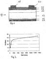
- positive charge was applied to the front of the corresponding solar cell by corona discharge. It became the parallel resistance according to the Fig. 2 measured. It can be seen that after initial reduction of the parallel resistance after about 15 minutes, a permanent regeneration occurs.
- FIG. 3 Another embodiment of a solar cell 100 is the Fig. 3 refer to.
- an optically transparent electrically conductive layer 28 which may consist of indium-tin oxide or zinc oxide is applied to the front-side silicon nitride layer 22.
- the layer 28 covers the anti-reflection layer 22 and can also extend over the front contacts 18, 20.
- the front contacts 18, 20 are left free. Independent of this is an electrically conductive connection between the layer 28 and the front contacts 18, 20 given.
- FIG. 4 a section of a corresponding module 30 with a solar cell 10 is shown.
- the solar cells 110 front and back of a transparent plastic layer of z. B. ethylene vinyl acetate (EVA) surrounded and embedded in these.
- EVA ethylene vinyl acetate
- the corresponding layers are identified by the reference numerals 32, 34.
- the rear side along the EVA layer 34 extends a backsheet 36, the z. B. of polyvinyl fluoride (TEDLAR) may exist.
- the EVA layer 32 is covered by a glass plate 38. The unit formed in this way is surrounded by a metal frame that is grounded.
- a transparent electrically conductive layer 40 is arranged, which may consist of indium tin oxide or zinc oxide.
- the corresponding layer 40 is then connected to one of the poles of the module, ie with the plus or minus pole.
Description
Die Erfindung bezieht sich auf eine kristalline Solarzelle mit einem p-grunddotierten Substrat und einem frontseitigen n-dötierten Bereich und einem rückseitigen p-dotieren Bereich, einem Frontseitenkontakt, einem Rückseitenkontakt und zumindest einer frontseitigen ersten Schicht aus SiN oder SiN enthaltend wie Antireflexiohsschicht. Auch nimmt die Erfindung Bezug auf ein Verfahren zur Herstellung einer kristallinen Solarzelle mit p-grunddotiertem Substrat und einem frontseitigen n-dotierten Bereich, rückseitigem p-dotierten Bereich, Front- und Rückseitenkontakten sowie zumindest einer frontseitigen Schicht aus SiN oder SiN enthaltend als erste Schicht wie Antireflexionsschicht.The invention relates to a crystalline solar cell with a p-type doped substrate and a front n-doped region and a back p-doped region, a front side contact, a rear contact and at least one front side first layer of SiN or SiN containing such as Antireflexiohsschicht. The invention also relates to a method for producing a crystalline solar cell with p-type doped substrate and a front-side n-doped region, rear p-doped region, front and back contacts and at least one front layer of SiN or SiN containing as a first layer such as antireflection coating.
Die n- und p-dotierten Bereiche in einer pn-Diode erzeugen eine Raumladungszone, in der Elektronen aus der n-Schicht in die p-Schicht und Löcher der p-Schicht in die n-Schicht wandern. Wenn eine Spannung an die sich auf den n- und p-dotierten Schichten befindenden metallischen Elektroden gelegt wird, fließt ein hoher Strom, wenn die Spannung an der negativen Elektrode negativ ist. Bei umgekehrter Polung fließt ein wesentlich geringerer Strom.The n- and p-doped regions in a pn diode create a space charge zone in which electrons migrate from the n-layer into the p-layer and holes of the p-layer into the n-layer. When a voltage is applied to the metallic electrodes located on the n- and p-doped layers, a high current flows when the Voltage at the negative electrode is negative. In reverse polarity flows a much lower current.
Eine besondere Ausführung von Si pn-Dioden sind Solarzellen oder Photodetektoren, bei denen ein Teil der Vorderseite mit einer mindestens teiltransparenten Schicht versehen ist, die meistens eine reflexionsmindennde Wirkung besitzt. Durch diese Schicht dringt Licht in das Silizium ein, welches dort zum Teil absorbiert wird. Dabei werden Überschusselektronen und -löcher freigesetzt. Die Überschusselektronen wandern im elektrischen Feld der Raumladungszone vom p-dotierten zum n-dotierten Bereich und schließlich zu den Metallkontakten auf dem n-dotierten Bereich, die Überschusslöcher wandern vom n-dotierten in den p-dotierten Bereich und schließlich zu den Metallköntakten auf dem p-dotierten Bereich. Wenn eine Last zwischen die positiven und negativen Elektroden gelegt wird, fließt ein Strom.A particular embodiment of Si pn diodes are solar cells or photodetectors, in which a part of the front side is provided with an at least partially transparent layer, which usually has a reflection-reducing effect. Through this layer, light penetrates into the silicon, which is partially absorbed there. Excessive electrons and holes are released. The excess electrons travel in the electric field of the space charge zone from the p-doped to the n-doped region and finally to the metal contacts on the n-doped region, the excess holes migrate from the n-doped to the p-doped region and finally to the metal kinetics on the p -doped area. When a load is placed between the positive and negative electrodes, a current flows.
In der Regel werden viele Solarzellen mit Hilfe von metallischen Verbindern in Reihe geschaltet und in einem Solarmodul bestehend aus mehreren Isolationsschichten einlaminiert, um sie vor Witterungseinflüssen zu schützen. Ein Problem ist, dass durch die Reihenschaltung der Solarzellen und die Reihenschaltung mehrerer Module zu einem System regelmäßig Systemspannungen von mehreren hundert Volt auftreten. Es ergeben sich hohe elektrische Felder zwischen Solarzellen und Erdpotential, die zu unerwünschten Verschiebung- und Ableitströmen führen. Dadurch können Ladungen auf der Oberfläche der Solarzellen dauerhaft deponiert werden, die deren Wirkungsgrad erheblich reduzieren können. Auch unter Beleuchtung oder langer Lagerung im Dunkeln können sich Ladungen auf der Oberfläche anreichern.As a rule, many solar cells are connected in series by means of metallic connectors and laminated in a solar module consisting of several insulation layers in order to protect them from the effects of the weather. One problem is that the series connection of the solar cells and the series connection of several modules to a system regularly system voltages of several hundred volts occur. This results in high electric fields between solar cells and ground potential, which lead to undesirable displacement and leakage currents. As a result, charges on the surface of the solar cell can be permanently deposited, which can significantly reduce their efficiency. Even under illumination or long storage in the dark, charges on the surface can accumulate.
Bekannt ist die Degradation der Leerlaufspannung und in geringerem Maß auch des Kurzschlussstroms aufgrund von Ladungen auf der Vorderseite von beidseitig kontaktierten Siliziumsolarzellen mit n-Grunddotierung und p-dotierter Vorderseite (
Beobachtet wurde die Degradation der Leerlaufspannung und des Kurzschlussstroms aufgrund von Ladungen auf der Vorderseite auch bei beidseitig kontaktierten Siliziumsolarzellen mit n-Grunddotierung, n-dotierter Vorderseite und p-dotierter Rückseite (J. Zhao, aaO). Sie degradieren ebenfalls stark unter Beleuchtung und langer Lagerung im Dunkeln aufgrund von Anreicherung negativer Ladungen im Siliziumnitrid und/oder Siliziumoxid auf der Vorderseite. Die negativen Ladungen führen in diesem Fall zur Verarmung der n-dotierten Siliziumoberfläche und damit wiederum zur Erhöhung der Oberflächenrekombinationsgeschwindigkeit. Charakteristisch ist auch in diesem Fall, dass der Parallelwiderstand und somit der Füllfaktor nicht beeinträchtigt werden.The degradation of the open circuit voltage and the short circuit current due to charges on the front side was also observed in the case of double sided silicon solar cells with n-type doping, n-doped front and p-doped back (J. Zhao, loc. Cit.). They also degrade greatly under illumination and long storage in the dark due to accumulation of negative charges in the silicon nitride and / or silica on the front. The negative charges lead in this case to the depletion of the n-doped silicon surface and thus in turn to increase the surface recombination speed. It is also characteristic in this case that the parallel resistance and thus the fill factor are not impaired.
Für Module, die rückseitig kontaktierte Solarzellen mit n-Grunddotierung, n-dotierter Vorderseite und lokalen p- und n-dotierten Bereichen auf der Rückseite des Substrats enthalten, ist eine Degradation aufgrund von Ladungen bekannt (siehe:
Ferner wurde in R. Swanson, aaO, zur Verhinderung der Ansammlung von Ladungen auf der Vorderseite von Solarzellen, bei denen sich alle pn-Übergänge und Metallkontakte auf der Rückseite des Substrats befinden, vorgeschlagen, einen leitenden Überzug auf die Antireflexschicht auf der Vorderseite aufzubringen und diesen Überzug mit dem Plus- oder Minuspol der Solarzellen auf der Rückseite leitend zu verbinden.Further, in R. Swanson, supra, in order to prevent the accumulation of charges on the front side of solar cells where all the pn junctions and metal contacts are on the back side of the substrate, it has been proposed to apply a conductive coating to the antireflection layer on the front side and To connect this coating with the positive or negative pole of the solar cells on the back conductive.
Beidseitig kontaktierte Siliziumsolarzellen mit p-Grunddotierung und n-dotierter Vorderseite sind gegenüber den oben beschriebenen Solarzelltypen wesentlich unempfindlicher auf Änderungen der Oberflächenrekombinationsgeschwindigkeit auf der Vorderseite. Deswegen wurde unter Beleuchtung und langer Lagerung im Dunkeln nur eine geringe Degradation der Leerlaufspannung festgestellt (J. Zhao, aaO).Both sides contacted silicon solar cells with p-type doping and n-doped front face are compared to the above-described types of solar cells much less sensitive to changes in the surface recombination speed on the front. Therefore, under illumination and long storage in the dark, only a small degradation of the open circuit voltage was found (J. Zhao, loc. Cit.).
In
Aus der
In der
Aus der
Der
In der
Aus der
Der
Gegenstand der
Die
Der vorliegenden Erfindung liegt die Aufgabe zu Grunde, eine kristalline Solarzelle, ein Verfahren zur Herstellung einer solchen sowie ein Verfahren zur Herstellung eines Solarzellenmoduls der eingangs erläuterten Arten so weiterzubilden, dass die Degradation des Parallelwiderstandes und somit des Füllfaktors verringert wird, insbesondere von beidseitig kontaktierten Siliziumsolarzellen mit p-Grunddotierung, n-dotierter Vorderseite und einer Antireflexschicht bestehend aus Siliziumnitrid, aufgrund von hohen negativen Systemspannungen oder positiven Ladungen auf der Vorderseite.The present invention is based on the object, a crystalline solar cell, a method for producing such and a method for producing a solar cell module of the initially described types so that the degradation of the parallel resistance and thus the fill factor is reduced, in particular contacted on both sides of the silicon solar cells with p-base doping, n-doped front and an antireflective layer consisting of silicon nitride due to high negative system voltages or positive charges on the front side.
Zur Lösung der Aufgabe sieht die Erfindung im Wesentlichen eine kristalline Solarzelle vor, die sich dadurch auszeichnet, dass zwischen der ersten Schicht und dem n-dotierten Bereich eine zweite Schicht aus zumindest einem Material aus der Gruppe SiN, SiOx, Al2Ox, SiOxNy: Hz, a-Si:H, TiOx oder ein solches Material enthaltend angeordnet und zur Bildung von Störstellen dotiert ist.To achieve the object, the invention provides essentially a crystalline solar cell before, which is characterized in that between the first layer and the n-doped region of a second layer of at least one material from the group of SiN, SiO x, Al 2 O x, SiO x N y : Hz, a-Si: H, TiO x or such material containing and doped to form impurities.
Die aus SiN bestehende oder SiN enthaltende zweite Schicht sollte ein Silizium-Stickstoff-Verhältnis von 1 bis 2,2 und eine H-Atomkonzentration von über 10 % enthalten.The SiN-containing or SiN-containing second layer should contain a silicon-nitrogen ratio of 1 to 2.2 and an H atomic concentration of more than 10%.
Um eine noch verbesserte Stabilität zu erzielen, ist vorgesehen, dass in der ersten Schicht positive und/oder negative Ladungsträger nach Herstellung der ersten Schicht eingelagert werden.In order to achieve an even better stability, it is provided that positive and / or negative charge carriers are incorporated in the first layer after the first layer has been produced.
Vorzugsweise beträgt die Flächenladungsdichte der Ladungsträger > 1·1012/cm2.The surface charge density of the charge carriers is preferably> 1 · 10 12 / cm 2 .
Insbesondere sollte nach Herstellung der Solarzelle an diese eine negative Spannung Un über eine vorgegebene Zeit angelegt werden.In particular, after the production of the solar cell, a negative voltage U n should be applied thereto over a predetermined time.
Auch zeichnet sich die Erfindung dadurch aus, dass nach Herstellung der Solarzelle auf diese positive Ladungen aufgebracht werden.Also, the invention is characterized in that after production of the solar cell to these positive charges are applied.
Sofern die zweite Schicht aus SiN besteht oder SiN enthält, sollte diese einen Brechungsindex n mit n ≥ 2, insbesondere zwischen 2,1 und 3,0 aufweisen.If the second layer consists of SiN or contains SiN, this should have a refractive index n with n ≥ 2, in particular between 2.1 and 3.0.
Vorzugsweise sollte die zweite Schicht mit einer Dicke D2 mit 1 nm ≤ D2 ≤ 50 nm ausgebildet werden.Preferably, the second layer should be formed with a thickness D 2 of 1 nm ≦ D 2 ≦ 50 nm.
Überraschenderweise hat sich gezeigt, dass dann, wenn in die frontseitige Siliziumnitridschicht oder eine zwischen dieser und dem n-dotierten Bereich der Solarzelle vorhandene Siliziumnitridschicht Störstellen eingebracht werden, die Degradation des Parallelwiderstandes stark verhindert bzw. zumindest stark verringert wird. Die Störstellen werden insbesondere durch Dotierung mit einem Element aus der Gruppe P, N, Sb, Bi, C, O, B, Al, Ga, In, Tl, Cu, V, W, Fe, Cr erzeugt.Surprisingly, it has been found that if impurities are introduced into the front-side silicon nitride layer or a silicon nitride layer present between it and the n-doped region of the solar cell, the degradation of the parallel resistance is greatly prevented or at least greatly reduced. The impurities are generated in particular by doping with an element from the group P, N, Sb, Bi, C, O, B, Al, Ga, In, Tl, Cu, V, W, Fe, Cr.
Anstelle der Siliziumnitridschicht kann auch eine Schicht aus einem anderen Material, vorzugsweise SiOx, Al2Ox, SiOxNy:Hz, a-Si, a-Si:H oder TiOx vorgesehen sein.Instead of the silicon nitride layer, it is also possible to provide a layer of another material, preferably SiO x , Al 2 O x , SiO x N y : H z , a-Si, a-Si: H or TiO x .
In der zweiten Schicht können Störstellen durch Dotierung mit zumindest einem Element aus der Gruppe P, N, Sb, Bi, C, O, B, Al, Ga, In, Tl, Cu, V, W, Fe, Cr erzeugt werden.In the second layer, impurities can be generated by doping with at least one of P, N, Sb, Bi, C, O, B, Al, Ga, In, Tl, Cu, V, W, Fe, Cr.
In einer Ausführungsform besteht die Schicht aus SiOx, das mittels UV-Beleuchtung des Siliziumsubstrats mit Wellenlängen λ < 400 nm in sauerstoffhaltiger Atmosphäre erzeugt wurde. In einer anderen Ausführungsform besteht die Schicht aus SiOx, das bei Temperaturen im Bereich zwischen 300 und 1000°C in sauerstoffhaltiger Atmosphäre erzeugt wurde.In one embodiment, the layer consists of SiO x , which was produced by means of UV illumination of the silicon substrate with wavelengths λ <400 nm in an oxygen-containing atmosphere. In another embodiment, the layer consists of SiO x , which was produced at temperatures in the range between 300 and 1000 ° C in an oxygen-containing atmosphere.
Durch die zusätzliche Schicht wird die Ausbildung von niedrigen Parallelwiderständen bei hohen negativen Systemspannungen oder nach dem Aufbringen positiver Ladungen auf die Vorderseite der Solarzellen im Vergleich zu anderen Solarzellen, bei denen die Siliziumnitridschicht direkt auf die n-dotierte Vorderseite abgeschieden wurde, stark verringert.The additional layer greatly reduces the formation of low shunt resistances at high negative system voltages or after the application of positive charges to the front side of the solar cells compared to other solar cells in which the silicon nitride layer has been deposited directly on the n-doped front side.
Des Weiteren zeichnet sich die Erfindung durch ein Verfahren zur Herstellung einer kristallinen Solarzelle mit frontseitigem n-dotierten Bereich, rückseitigem p-dotieren Bereich, Front- und Rückseitenkontakten sowie zumindest einer frontseitigen Schicht aus SiN oder SiN enthaltend als erste Schicht wie Antireflexionsschicht dadurch aus, dass zwischen der ersten Schicht und dem n-dotierten Bereich eine als zweite Schicht angeordnet wird, die aus zumindest einem der Materialien aus der Gruppe SiN, SiOx, Al2Ox, SiOxNy:Hz, a-Si:H, TiOx besteht oder dieses enthält, dass nach Herstellung der Solarzelle entweder an die Solarzelle eine negative Spannung Un angelegt wird oder in die erste Schicht positive und/oder negative Ladungsträger eingebracht werden. Ferner sollte die zweite Schicht zur Bildung von Störstellen mit vorzugsweise ein Element aus der Gruppe P, N, Sb, Bi, C, O, B, Al, Ga, In, Tl, Cu, V, W, Fe, Cr dotiert sein.Furthermore, the invention is characterized by a method for producing a crystalline solar cell with front-side n-doped region, back p-doped region, front and back contacts and at least one front-side layer of SiN or SiN containing as the first layer such as anti-reflection layer in that between the first layer and the n-doped region is arranged as a second layer, which consists of at least one of the materials from the group SiN, SiO x , Al 2 O x , SiO x N y : Hz, a-Si: H, TiO x exists or this contains that after production of the solar cell either to the solar cell, a negative voltage U n is applied or in the first layer positive and / or negative charge carriers are introduced. Further, the second impurity-forming layer should preferably be doped with one of P, N, Sb, Bi, C, O, B, Al, Ga, In, Tl, Cu, V, W, Fe, Cr.
Somit sieht eine weitere Lösung der Aufgabe vor, dass die Solarzelle - wie oben beschrieben - mit einer zusätzlichen Schicht zwischen Siliziumsubstrat und Siliziumnitridschicht ausgestattet wird und zusätzlich positive Ladungen auf die Solarzelle aufgebracht werden. Dabei befindet sich die Solarzelle vorteilhafterweise bei Temperaturen im Bereich von 10°C bis 600°C.Thus, another solution to the problem provides that the solar cell - as described above - is equipped with an additional layer between the silicon substrate and silicon nitride layer and in addition positive charges are applied to the solar cell. In this case, the solar cell is advantageously at temperatures in the range of 10 ° C to 600 ° C.
Eine Lösung der Aufgabe sieht ferner vor, dass die Solarzelle - wie oben beschirieben - mit einer zusätzlichen Schicht zwischen Siliziumsubstrat und Siliziumnitridschicht ausgestattet wird und nach Einlamination in ein Modul der Solarzellverbund vorübergehend gegenüber Erde mit hoher negativer Spannung beaufschlagt wird. Dabei sollte sich das Modul bei Temperaturen im Bereich von 10 °C bis 220 °C befinden.A solution of the problem further provides that the solar cell - as described above - is equipped with an additional layer between the silicon substrate and silicon nitride layer and after lamination into a module of the solar cell assembly is temporarily applied to earth with high negative voltage. The module should be at temperatures in the range of 10 ° C to 220 ° C.
Überraschenderweise wurde gefunden, dass mit fortschreitendem Aufbringen positiver Ladungen auf die Solarzelle bzw. mit fortschreitendem Anlegen hoher negativer Spannung an das Modul gegenüber Erde der Parallelwiderstand der Solarzelle bzw. des Solarmoduls zunächst abnimmt, dann jedoch wieder nahezu auf den Ausgangswert ansteigt und somit die Degradation praktisch vollständig rückgängig gemacht wird. Auf diesem hohen Wert verbleibt der Parallelwiderstand dauerhaft, auch wenn keine zusätzlichen positiven Ladungen mehr auf die Solarzelle aufgebracht werden bzw. keine negative Spannung mehr an dem Solarzellverbund im Modul gegenüber Erde anliegt. Hohe Temperaturen beschleunigen diesen Prozess der dauerhaften Regeneration.Surprisingly, it has been found that with the progressive application of positive charges to the solar cell or with progressive application of high negative voltage to the module to earth, the parallel resistance of the solar cell or the solar module initially decreases, but then almost increases again to the initial value and thus the degradation practically completely undone. At this high value, the parallel resistor remains permanently, even if no additional positive charges are applied to the solar cell or no negative voltage is applied to the solar cell assembly in the module to earth. High temperatures accelerate this process of permanent regeneration.
Insbesondere sollte bei einer Temperatur zwischen 50° C und 200° C, bevorzugt 80° C, eine negative Spannung an die Solarzelle angelegt und/oder in die erste Schicht positive und/oder negative Ladungen eingebracht werden.In particular, at a temperature between 50 ° C. and 200 ° C., preferably 80 ° C., a negative voltage should be applied to the solar cell and / or positive and / or negative charges should be introduced into the first layer.
Das erfindungsgemäße Verfahren unterscheidet sich grundlegend von der vorübergehenden Regeneration, die für Solarzellen ohne zusätzliche Schicht zwischen Siliziumsubstrat und Siliziumnitridschicht bekannt ist und beim Anlegen einer positiven Spannung beobachtet wurde.The inventive method is fundamentally different from the temporary regeneration, which is known for solar cells without additional layer between silicon substrate and silicon nitride layer and was observed when applying a positive voltage.
Ein weiterer Lösungsvorschlag der der Erfindung zu Grunde liegenden Aufgabe sieht vor, dass auf die beidseitig kontaktierten Siliziumsolarzellen mit p-Grunddotierung, n-dotierter Vorderseite und einer Antireflexschicht bestehend aus Siliziumnitrid ein optisch transparenter leitfähiger Überzug auf die Vorderseite aufgebracht wird. Dadurch werden Antireflexschicht und die Vorderseiten-Metallkontakte ohne weitere zusätzliche Maßnahmen leitend miteinander verbunden. Weil Vorderseiten-Metallkontakte wiederum elektrisch leitend mit der n-dotierten Vorderseite verbunden sind, bleibt die Antireflexschicht auch bei hohen Systemspannungen frei von elektrischen Feldern und es werden somit keine Ladungen in die Antireflexschicht eingebracht.A further solution proposed by the invention is based on the object that an optically transparent conductive coating is applied to the front side of the silicon solar cells with p-type doping, n-doped front side and an antireflection layer consisting of silicon nitride which are contacted on both sides. As a result, the antireflection layer and the front-side metal contacts are conductively connected to one another without further additional measures. Because front-side metal contacts are in turn electrically conductively connected to the n-doped front side, the antireflection layer remains free of electric fields even at high system voltages and thus no charges are introduced into the antireflection layer.
Ein Verfahren zur Herstellung eines Solarzellenmoduls der eingangs genannten Art zeichnet sich dadurch aus, dass der Rahmen gegenüber zumindest einem Anschluss des Solarzellenmoduls mit einer hohen positiven elektrischen Spannung über eine vorgegebene Zeit beaufschlagt wird. Dabei ist insbesondere vorgesehen, dass zwischen dem Rahmen und dem zumindest einen elektrischen Kontakt eine positive elektrische Spannung zwischen 100 V und 20.000 V angelegt wird, wobei vorzugsweise die positive elektrische Spannung über eine Zeit t1 mit 0,5 sec ≤ t1 ≤ 1200 min angelegt wird.A method for producing a solar cell module of the type mentioned above is characterized in that the frame is subjected to a high positive electrical voltage over a predetermined time compared to at least one terminal of the solar cell module. It is provided in particular that between the frame and the at least one electrical contact, a positive electrical voltage between 100 V and 20,000 V is applied, wherein preferably the positive electrical voltage over a time t 1 with 0.5 sec ≤ t 1 ≤ 1200 min is created.
Eine alternative Lösung zur Herstellung eines Solarzellenmoduls sieht vor, dass auf das Solarzellenmodul über eine Zeit t2 eine elektrisch leitende Flüssigkeit, eine elektrisch leitende Kunststöfffolie oder eine elektrisch leitende Metallfolie aufgebracht und an dieser gegenüber zumindest einem der elektrischen Kontakte des Solarzellenmoduls über eine vorgegebene Zeit t3 eine hohe positive elektrische Spannung angelegt wird. Dabei sollte zwischen der leitenden Flüssigkeit bzw. der Kunststofffolie bzw. der Metallfolie und dem zumindest einen elektrischen Kontakt eine positive elektrischen Spannung zwischen 100 V und 20.000 V angelegt werden.An alternative solution for producing a solar cell module provides that applied to the solar cell module for a time t 2, an electrically conductive liquid, an electrically conductive Kunststöfffolie or an electrically conductive metal foil and at this against at least one of the electrical contacts of the solar cell module over a predetermined time t 3, a high positive voltage is applied. In this case, a positive electrical voltage between 100 V and 20,000 V should be applied between the conductive liquid or the plastic film or the metal foil and the at least one electrical contact.
Insbesondere ist vorgesehen, dass die Flüssigkeit bzw. Kunststofffolie bzw. Metallfolie über eine Zeit t2 mit 0,5 sec ≤ t2 ≤ 1200 min auf dem Solarzellenmodul angeordnet wird bzw. die positive elektrischen Spannung über eine Zeit t3 mit 0,5 sec ≤ t3 ≤ 1200 min angelegt wird.In particular, it is provided that the liquid or plastic film or metal foil over a time t 2 with 0.5 sec ≤ t 2 ≤ 1200 min is placed on the solar cell module or the positive electrical voltage over a time t 3 with 0.5 sec ≤ t 3 ≤ 1200 min is applied.
Des Weiteren bezieht sich ein gattungsgemäßes Beispiel auf ein Solarzellenmodul umfassend vershal tete kristalline p- oder n-Solarzellen, die jeweils einen frontseitigen n- oder p-dotieren Bereich, einen rückseitigen p- oder n-dotierten Bereich, einen Frontseitenkontakt, einen Rückseitenkontakt, zumindest eine frontseitige Schicht aus SiN oder SiN enthaltend, wobei die Solarzellen frontseitig von einem optisch transparenten Einbettmaterial aus Kunststoff abgedeckt sind, über dem Einbettmaterial eine elektrisch isolierende, optisch transparente Abdeckung aus Glas oder Kunststoff angeordnet ist, die Solarzellen rückseitig von einem Einbetmaterial aus Kunststoff abgedeckt sind und so gebildete Einheit von einem umlaufenden metallischen Rahmen umgeben ist, und zeichnet sich dadurch aus, dass zwischen dem frontseitigen Kunststoffeinbettmaterial und der Abdeckung eine elektrisch leitende sowie optisch zumindest teiltransparente Schicht angeordnet wird, die elektrisch leitend mit einem der elektrischen Kontakte des Solarzellenmoduls verbunden wird.Furthermore, a generic example relates to a solar cell module comprising vershal tete crystalline p or n solar cells, each having a front-side n- or p-doped region, a rear p- or n-doped region, a front side contact, a back contact, at least a front-side layer comprising SiN or SiN, wherein the solar cells are covered on the front side by an optically transparent embedding material made of plastic, an electrically insulating, optically transparent cover made of glass or plastic is arranged over the embedding material, the solar cells are covered on the back by a plastic embedding material and thus formed unit is surrounded by a circumferential metallic frame, and is characterized in that between the front-side Kunststoffeinbettmaterial and the cover, an electrically conductive and optically at least partially transparent layer is arranged, the electrically conductive with a the electrical contacts of the solar cell module is connected.
Aufgrund der erfindungsgemäßen Lehren wird die Degradation des Parallelwiderstands zu dem pn-Übergang zumindest reduziert bzw. dauerhaft vermieden, so dass der Wirkungsgrad der Solarzellen und damit des Solarzellenmoduls nicht unzulässig verringert wird. Dabei wird nach einem Lösungsvorschlag zur dauerhaften Regeneration eines zunächst reduzierten Parallelwiderstands eine Gleichspannung zwischen zumindest einem Anschluss der Solarzelle bzw. des Solarzellenmoduls und Erde angelegt, und zwar bei p-dotierten kristallinen Siliziumsolarzellen mit p-dotierten Substrat und n-dotieiter Frontseite eine negative Spannung, sofern eine Zwischenschicht eingebaut wird, die nicht aus Siliziumnitrid besteht, sondern eine solche, die bevorzugterweise aus zumindest einem Material aus der Gruppe SiOx, Al2Ox, SiOxNy:Hz, a-Si:H, TiOx besteht.Due to the teachings of the invention, the degradation of the parallel resistance to the pn junction is at least reduced or permanently avoided, so that the efficiency of the solar cell and thus of the solar cell module is not unduly reduced. In this case, a DC voltage between at least one terminal of the solar cell or of the solar cell module and earth is applied after a proposed solution for the permanent regeneration of an initially reduced parallel resistance, namely for p-doped crystalline silicon solar cells with p-doped substrate and n-type front side a negative voltage, if an intermediate layer is used which does not consist of silicon nitride, but one which preferably consists of at least one material from the group SiO x , Al 2 O x , SiO x N y : Hz, a-Si: H, TiO x .
Eine Störstellen aufweisendes Siliziumnitridschicht- sei es eine Zwischenschicht, sei es die frontseitige Siliziumnitridschicht wie Antireflexschicht - bedarf einer diesbezüglichen Spannungsanlegung nicht.An impurity having Siliziumnitridschicht- be it an intermediate layer, be it the front side Siliziumnitridschicht such as anti-reflection layer - does not require a relevant voltage application.
Anstelle der Spannungsanlegung kann auch ein Einbringen von insbesondere negativen Ladungsträgern in die frontseitige Siliziumnitridschicht erfolgen, die die gleiche Wirkung herbeiführen. Damit die negativen Ladungsträger eingebracht werden können, werden auf die Oberseite der Solarzelle vorzugsweise mittels Koronaentladung positive Ladungen aufgebracht. Auch in diesem Fall tritt nach anfänglicher Reduktion des Parallelwiderstandes eine dauerhafte Regeneration ein.Instead of the voltage application, it is also possible to introduce particularly negative charge carriers into the front-side silicon nitride layer, which bring about the same effect. In order for the negative charge carriers to be introduced, positive charges are preferably applied to the upper side of the solar cell by means of corona discharge. Also in this case occurs after initial reduction of the parallel resistance, a permanent regeneration.
Das Einbringen der Ladungsträger in die Siliziumnitridschicht erfolgt dadurch, dass durch das Aufbringen der positiven Ladungsträger aus dem Siliziumnitrid negative Ladungsträger in die Siliziumnitridschicht gelangen und dort verbleiben, so dass anschließend die positiven Ladungen von der Oberseite der Solarzelle entfernt werden können.The introduction of the charge carriers into the silicon nitride layer takes place in that, by applying the positive charge carriers from the silicon nitride, negative charge carriers enter the silicon nitride layer and remain there, so that subsequently the positive charges can be removed from the upper side of the solar cell.
Ein Einbringen von Ladungsträgern bzw. ein Anlegen einer hohen Spannung ist auch dann nicht erforderlich, wenn die Solarzellen an ihrer Oberseite oder die Solarzellenmoduls vorzugsweise über die die einzelnen Solarzellen einbettende Isolationsschicht wie EVA mit einer elektrisch leitenden, optisch zumindest teiltransparenten Schicht abgedeckt sind, die sodann bei unmittelbarem Auftragen auf die Solarzelle mit dem vorzugsweise streifen- oder punktförmigen Frontkontakt oder bei Aufbringen auf die Isolationsschicht wahlweise mit dem Front- oder Rückkontakt verbunden wird.An introduction of charge carriers or the application of a high voltage is not required even if the solar cells are covered on their upper side or the solar cell module preferably via the insulating layer embedding the individual solar cells such as EVA with an electrically conductive, optically at least partially transparent layer, then the is directly connected to the solar cell with the preferably strip or punctiform front contact or when applied to the insulating layer optionally connected to the front or back contact.
Daher zeichnet sich die Erfindung nach einem selbständigen Lösungsvorschlag auch durch eine kristalline Solarzelle mit einem fronstseitig n-dotierten Bereich, einem rückseitigen p-dotierten Bereich, einem Frontseitenkontakt, einem Rückseitenkontakt und zumindest einer frontseitigen ersten Schicht aus SiN oder SiN enthaltend wie Antireflexionsschicht dadurch aus, dass auf der ersten Schicht oder einer über dieser verlaufenden Isolationsschicht eine elektrisch leitende und optisch zumindest teiltransparente dritte Schicht angeordnet ist, die bei einer Anordnung auf der ersten Schicht mit dem Frontkontakt und bei einer Anordnung auf der Isolationsschicht mit dem Front- oder Rückkontakt elektrisch leitend verbunden ist.Therefore, according to an independent solution proposal, the invention is also characterized by a crystalline solar cell with a fronstseitig n-doped region, a backside p-doped region, a front side contact, a rear side contact and at least one front side first layer of SiN or SiN such as anti-reflection layer, in that an electrically conductive and optically at least partially transparent third layer is arranged on the first layer or an insulating layer running over it, which in an arrangement on the first layer is connected to the first layer Front contact and in an arrangement on the insulating layer with the front or rear contact is electrically connected.
Weitere Einzelheiten, Vorteile und Merkmale der Erfindung ergeben sich nicht nur aus den Ansprüchen, den diesen u entnehmenden Merkmalen - für sich und/oder in Kombination -, sondern auch aus der nachfolgenden Beschreibung der bevorzugten Ausführungsbeispiele und den Zeichnungen.Further details, advantages and features of the invention will become apparent not only from the claims, the features taking these u out - alone and / or in combination - but also from the following description of the preferred embodiments and the drawings.
Es zeigen:
- Fig. 1
- eine erste Ausführungsform der Siliziumsolarzelle mit verbesserter Stabilität bei hohen negativen Systemspannungen,
- Fig. 2
- gemessenen Parallelwiderstand einer Siliziumsolarzelle mit verbesserter Stabilität bei hohen negativen Systemspannungen als Funktion der Beladungszeit mit positiven Landungen,
- Fig. 3
- eine weitere Ausführungsform der Siliziumsolarzelle mit verbesserter Stabilität bei hohen negativen Systemspannungen und
- Fig. 4
- eine Ausführungsform eines Solarmoduls mit verbesserter Stabilität bei hohen Systemspannungen.
- Fig. 1
- a first embodiment of the silicon solar cell with improved stability at high negative system voltages,
- Fig. 2
- measured parallel resistance of a silicon solar cell with improved stability at high negative system voltages as a function of the loading time with positive landings,
- Fig. 3
- a further embodiment of the silicon solar cell with improved stability at high negative system voltages and
- Fig. 4
- an embodiment of a solar module with improved stability at high system voltages.
Bei der nachfolgenden Beschreibung von bevorzugten Ausführungsbeispielen wird unterstellt, dass der Aufbau und die Funktion einer Solarzelle bzw. eines Solarzellenmoduls hinlänglich bekannt sind, insbesondere in Bezug auf p-grunddotierte kristalline Siliziumsolarzellen und aus diesen hergestellten Module.In the following description of preferred exemplary embodiments, it is assumed that the construction and the function of a solar cell or of a solar cell module are well known, in particular with regard to p-type doped crystalline silicon solar cells and modules produced therefrom.
Des Weiteren ist anzumerken, dass die Erfindung auch Solarzellen einschließt, die frontseitig mehrere Siliziumnitridschichten aufweisen, wie dies nach dem Stand der Technik bekannt ist. Insoweit ist der Begriff frontseitige Siliziumnitridschicht als Synonym für ein oder mehrere frontseitige Siliziumnitridschichten zu verstehen. Ferner sind die angegebenen Dimensionierungen grundsätzlich rein beispielhaft zu verstehen, ohne dass hierdurch die erfindungsgemäße Lehre eingeschränkt wird.It should also be noted that the invention also includes solar cells having a plurality of silicon nitride layers on the front side, as known in the art. In that regard, the term front side silicon nitride layer is to be understood as a synonym for one or more front side silicon nitride layers. Further are The stated dimensions should be understood as being purely exemplary, without this limiting the teaching according to the invention.
In
Erfindungsgemäß ist nach einer Ausführungsform zwischen der frontseitigen oder ersten Siliziumnitridschicht 22 und dem n+-diffundierten Bereich 14 eine weitere als zweite Schicht zu bezeichnende Siliziumnitridschicht 26 angeordnet, die einen Brechungsindex von z. B. 2,3 und eine Dicke von 25 nm aufweist.According to the invention, according to one embodiment, between the front-side or first
Durch das Aufbringen der Zwischenschicht, also zweiten Schicht 26 zwischen der Antireflexionsschicht 22 und dem n+-Bereich 14 wird erreicht, dass eine Degradation des Parallelwiderstands zu dem pn-Übergang, der zwischen den Schichten 12, 14 besteht, vermieden bzw. stark verringert wird. Die Zwischenschicht 26 weist durch Dotierungen Störstellen bzw. -bereiche auf. Als Dotierungen kommt bevorzugterweise ein Element aus der Gruppe P, N, Sb, Bi, C, O, B, Al, Ga, In, Tl, Cu, V, W, Fe, Cr Frage.By applying the intermediate layer, ie the
Eine Degradation des Parallelwiderstandes muss vermieden werden, da dann, wenn dieser zu stark abnimmt, quasi ein Kurzschluss im pn-Übergang auftritt, so dass die Solarzelle nicht mehr ordnungsgemäß arbeiten kann.Degradation of the parallel resistor must be avoided, because if it decreases too much, a short circuit in the pn junction occurs, so that the solar cell can no longer work properly.
Anstelle der aus Siliziumnitrid bestehenden Zwischenschicht 26 kann zur Vermeidung der Degradation des Parallelwiderstandes in Folge von hohen Systemspannungen und der Ladung auf der Vorderseite der Solarzelle bzw. eines aus entsprechenden Solarzellen bestehenden Moduls eine Schicht aus einem anderen Material wie SiOx, Al2Ox, Si-OxNy:Hz, a-Si:H und/oder TiOx eingefügt werden. In diesem Fall wird nach der Herstellung der Solarzelle bzw. dem Verschalten entsprechender Solarzellen zu einem Modul an einem der Kontakte der Solarzelle bzw. des Solarzellenmoduls, also an den Plus- oder Minus-Pol oder an beiden Kontakten eine hohe negative Gleichspannung gegenüber Erde angelegt. Als Dotierung für die Schicht kommt insbesondere ein Element aus der Gruppe P, N, Sb, Bi, C, O, B, Al, Ga, In, Tl, Cu, V, W, Fe, Cr in Frage.Instead of the
Alternativ können auf die Solarzelle, und zwar auf deren Vorderseite, positive Ladungen z. B. mittels einer Koronaentladung aufgebracht werden. Hierdurch werden in die entsprechende Zwischenschicht insbesondere negative Ladungen eingebracht, die aus der n+-Schicht stammen, wodurch gleichfalls eine entsprechende Degradation verhindert bzw. reduziert wird. Dies soll anhand der
Eine weitere Ausführungsform einer Solarzelle 100 ist der
Erfindungsgemäße Solarzellen zuvor erläuterter Art werden zu Solarzellenmodulen verschaltet, um eine verbesserte Stabilität dieser bei hohen Systemspannungen zu erzielen. In
In bekannter Weise werden die Solarzellen 110 vorder- und rückseitig von einer transparenten Kunststoffschicht aus z. B. Ethylenvinylacetat (EVA) umgeben und in diese eingebettet. Die entsprechenden Schichten sind mit den Bezugszeichen 32, 34 gekennzeichnet. Ferner erstreckt sich rückseitig entlang der EVA-Schicht 34 eine Rückseitenfolie 36, die z. B. aus Polyvinylfluorid (TEDLAR) bestehen kann. Frontseitig wird die EVA-Schicht 32 von einer Glasplatte 38 abgedeckt. Die so gebildete Einheit wird von einem Rahmen aus Metall umgeben, der auf Masse liegt.In a known manner, the solar cells 110 front and back of a transparent plastic layer of z. B. ethylene vinyl acetate (EVA) surrounded and embedded in these. The corresponding layers are identified by the
Zwischen der frontseitigen EVA-Schicht 32 und der Glasscheibe 38 ist eine transparente elektrisch leitfähige Schicht 40 angeordnet, die aus Indium-Zinn-Oxid oder Zink-Oxid bestehen kann. Die entsprechende Schicht 40 ist sodann mit einem der Pole des Moduls, also mit dem Plus- oder Minus-Pol verbunden. Eine diesbezügliche Anordnung bietet gleichfalls die Vorteile, wie diese auch im Zusammenhang mit der
Anstelle der Solarzelle 110 können auch Solarzellen 10, 100 oder solche zu einem Modul verschaltet werden, die entsprechend zuvor erfolgter Erläuterungen der erfindungsgemäßen Lehre folgen.Instead of the solar cell 110, it is also possible to connect
Claims (19)
- A crystalline solar cell (10, 100, 110) with a p-basic doped substrate (12), a front-side n-doped area (14), a back-side p-doped area (16), a front-side contact (18, 20), a back-side contact (24), and at least one front-side first layer (22) made of SiN or containing SiN as an anti-reflection layer,
characterized in that
between the first layer (22) and the n-doped area (14), a second layer (26) made of at least one material from the group SiN, SiOx, Al2Ox, SiOxNy:Hz, a-Si:H, TiOx, or containing such a material is arranged and is doped for the creation of imperfections. - The solar cell according to claim 1,
characterized in that
the second layer (26) composed of SiN or containing SiN has a refractive index n of n ≥ 2, in particular 2.1 ≤ n ≤ 3.0. - The solar cell according to claim 1,
characterized in that
the second layer composed of SiN or containing SiN contains a silicon-nitrogen ratio of 1 to 2.2 and an H-atom concentration of greater than 10%. - The solar cell according to at least claim 1,
characterized in that
that positive and/or negative charge carriers are incorporated into the first layer (22) after producing the first layer. - The solar cell according to at least claim 4,
characterized in that
the charge density of the charge carriers per unit area is > 1 × 10¹²/cm2. - The solar cell according to claim 1,
characterized in that
an electrically conducting and at least partially optically transparent third layer (28) is disposed on the first layer (22) or on an insulation layer extending over it, said third layer being connected in an electrically conductive manner to the front contact (18, 20) for an arrangement on the first layer and to the front or back contact for an arrangement on the insulation layer. - The solar cell according to at least one of the preceding claims,
characterized in that
the second layer (26) has a thickness D2 of 1 nm ≤ D2 ≤ 50 nm. - The solar cell according to at least one of the preceding claims,
characterized in that
in particular the second layer is an SiOx layer that is formed from the n-doped area. - The solar cell according to at least one of the preceding claims,
characterized in that
the second layer (26) is doped with at least one element from the group P, N, Sb, Bi, C, O, B, Al, Ga, In, Tl, Cu, V, W, Fe, Cr. - The solar cell according to at least one of the preceding claims,
characterized in that
the third layer (28) is composed of or contains indium tin oxide or zinc oxide. - The solar cell according to at least one of the preceding claims,
characterized in that
in the case of formation of the second layer from a material other than SiN, the first layer has a refractive index of n ≥ 2.0, or in the case of formation of the second layer (26) from SiN or when it contains SiN, the refractive index of the first layer is smaller than that of the second layer. - The solar cell according to at least one of the preceding claims,
characterized in that
the solar cell (10, 100, 110) has a negative system voltage. - A method for producing a crystalline solar (10, 100, 110) cell with a p-basic doped substrate (12), a front-side n-doped area (14), a back-side p-doped area (16), a front-side contact (18), a back-side contact (20), and at least one front-side first layer (22) made of SiN or containing SiN, as an anti-reflection layer,
characterized in that,
between the first layer (22) and the n-doped area (14), a second layer made of at least one material from the group SiOx, Al2Ox, SiOxNy:Hz, a-Si:H, TiOx, or containing such a material is disposed and is doped for the creation of imperfections, that, after producing the solar cell (10, 100, 110), either a negative voltage Un is applied to the solar cell or else positive and/or negative charge carriers are introduced into the first layer. - The method according to claim 13,
characterized in that
the second layer (26) is doped with at least one element from the group P, N, Sb, Bi, C, O, B, Al, Ga, In, Tl, Cu, V, W, Fe, Cr. - The method according to claim 13,
characterized in that
the charge carriers are introduced into the first layer (22) by deposition of positive charges on the front side of the solar cell (10, 100, 110) at a temperature T2 with 10 °C ≤ T2 ≤ 600 °C, wherein in particular the positive charges are deposited on the front side of the solar cell by corona discharge. - The method according to claim 13 or 15,
characterized in that
a negative voltage is applied to the solar cell and/or positive and/or negative charges are introduced into the first layer at a temperature of between 50°C and 200°C, preferably 80°C. - The method according to at least claim 13,
characterized in that
an SiOx layer is formed as the second layer (26) from the n-doped area in an oxygen-containing atmosphere at a temperature T of 150°C ≤ T ≤ 1000°C, and in particular at a pressure of between 10-5 and 0.5 bar. - The method according to at least claim 13,
characterized in that
the second layer (26) is formed in the form of an SiOx layer from the n-doped area in an ozone-containing atmosphere or by use of an ozone-containing liquid. - The method according to at least claim 13,
characterized in that
the second layer (12), in particular the SiOx layer, is formed with a thickness D2 of 1 nm ≤ D2 ≤ 50 nm, wherein in particular the second layer in the form of the SiOx layer is formed from the n-doped area (14) in an oxygen-containing atmosphere by means of UV light with a wavelength λ of λ < 400 nm.
Priority Applications (1)
| Application Number | Priority Date | Filing Date | Title |
|---|---|---|---|
| HRP20180062TT HRP20180062T1 (en) | 2009-09-18 | 2018-01-15 | Crystalline solar cell and method for producing said type of solar cell |
Applications Claiming Priority (2)
| Application Number | Priority Date | Filing Date | Title |
|---|---|---|---|
| DE102009044052A DE102009044052A1 (en) | 2009-09-18 | 2009-09-18 | Crystalline solar cell, process for producing the same and process for producing a solar cell module |
| PCT/EP2010/063710 WO2011033070A2 (en) | 2009-09-18 | 2010-09-17 | Crystalline solar cell, method for producing said type of solar cell and method for producing a solar cell module |
Publications (2)
| Publication Number | Publication Date |
|---|---|
| EP2478564A2 EP2478564A2 (en) | 2012-07-25 |
| EP2478564B1 true EP2478564B1 (en) | 2017-11-08 |
Family
ID=43479668
Family Applications (1)
| Application Number | Title | Priority Date | Filing Date |
|---|---|---|---|
| EP10754749.9A Active EP2478564B1 (en) | 2009-09-18 | 2010-09-17 | Crystalline solar cell and method for producing said type of solar cell |
Country Status (9)
| Country | Link |
|---|---|
| US (1) | US9496424B2 (en) |
| EP (1) | EP2478564B1 (en) |
| JP (1) | JP5714588B2 (en) |
| KR (1) | KR20120067359A (en) |
| CN (1) | CN102498573B (en) |
| DE (1) | DE102009044052A1 (en) |
| HR (1) | HRP20180062T1 (en) |
| TW (1) | TWI517427B (en) |
| WO (1) | WO2011033070A2 (en) |
Families Citing this family (23)
| Publication number | Priority date | Publication date | Assignee | Title |
|---|---|---|---|---|
| CN103022166A (en) * | 2011-09-28 | 2013-04-03 | 杭州赛昂电力有限公司 | Solar cell taking copper-clad aluminum wire as back electrode and producing process of solar cell |
| US20130146136A1 (en) * | 2011-12-13 | 2013-06-13 | Kyoung-Jin Seo | Photovoltaic device and method of manufacturing the same |
| DE102012101456A1 (en) | 2012-02-23 | 2013-08-29 | Schott Solar Ag | Process for producing a solar cell |
| DE102012216416A1 (en) * | 2012-03-05 | 2013-09-05 | Roth & Rau Ag | Process for the production of optimized solar cells |
| CN102623565B (en) * | 2012-03-31 | 2014-10-01 | 光为绿色新能源股份有限公司 | Method for producing new cell |
| TWI565091B (en) * | 2012-07-13 | 2017-01-01 | 晶元光電股份有限公司 | Opto-electronic device |
| TWI483409B (en) * | 2012-09-12 | 2015-05-01 | Ever Energy Co Ltd | Solar cell and manufacturing method thereof |
| US9219174B2 (en) | 2013-01-11 | 2015-12-22 | Solarcity Corporation | Module fabrication of solar cells with low resistivity electrodes |
| CN104425633B (en) * | 2013-08-30 | 2016-11-16 | 中国科学院宁波材料技术与工程研究所 | A kind of dielectric passivation film and solaode and preparation method thereof |
| GB2521457A (en) * | 2013-12-20 | 2015-06-24 | Isis Innovation | Charge stabilized dielectric film for electronic devices |
| US9337369B2 (en) * | 2014-03-28 | 2016-05-10 | Sunpower Corporation | Solar cells with tunnel dielectrics |
| BE1021976B1 (en) * | 2014-05-02 | 2016-02-01 | Futech | SOLAR PANEL INSTALLATION AND METHOD FOR ACCELERATED REGENERATION AND / OR PREVENTING DEFECTS IN SOLAR PANELS |
| CN104103715B (en) * | 2014-06-30 | 2016-08-24 | 浙江晶科能源有限公司 | A kind of preparation method of double-decker ITO electrode crystal silicon solar energy battery |
| HUE047530T2 (en) * | 2014-07-01 | 2020-04-28 | Meyer Burger Germany Gmbh | Solar cell |
| US10309012B2 (en) | 2014-07-03 | 2019-06-04 | Tesla, Inc. | Wafer carrier for reducing contamination from carbon particles and outgassing |
| US9761744B2 (en) | 2015-10-22 | 2017-09-12 | Tesla, Inc. | System and method for manufacturing photovoltaic structures with a metal seed layer |
| EP3321973B1 (en) | 2016-11-09 | 2021-01-06 | Meyer Burger (Germany) GmbH | Crystalline solar cell having a transparent, conductive layer between the front contacts and method for manufacturing such a solar cell |
| US10672919B2 (en) * | 2017-09-19 | 2020-06-02 | Tesla, Inc. | Moisture-resistant solar cells for solar roof tiles |
| JP2019079916A (en) * | 2017-10-24 | 2019-05-23 | 株式会社カネカ | Back-contact type solar battery module |
| US11190128B2 (en) | 2018-02-27 | 2021-11-30 | Tesla, Inc. | Parallel-connected solar roof tile modules |
| DE102018108158B4 (en) * | 2018-04-06 | 2023-06-07 | Hanwha Q Cells Gmbh | Bifacial solar cell, solar module and manufacturing method for a bifacial solar cell |
| CN111463319B (en) * | 2020-04-09 | 2021-12-17 | 无锡优顺能源开发科技有限公司 | Silicon solar cell and manufacturing method thereof |
| CN113782638A (en) * | 2021-09-09 | 2021-12-10 | 海宁正泰新能源科技有限公司 | Battery back passivation structure, manufacturing method thereof and solar battery |
Citations (3)
| Publication number | Priority date | Publication date | Assignee | Title |
|---|---|---|---|---|
| EP1304748A2 (en) * | 2001-10-19 | 2003-04-23 | RWE Solar GmbH | Method for producing a solar cell |
| WO2008098407A1 (en) * | 2007-02-08 | 2008-08-21 | Suntech Power Co., Ltd | Hybrid silicon solar cells and method of fabricating same |
| US20090151782A1 (en) * | 2007-12-18 | 2009-06-18 | Lg Electronics Inc. | Hetero-junction silicon solar cell and fabrication method thereof |
Family Cites Families (26)
| Publication number | Priority date | Publication date | Assignee | Title |
|---|---|---|---|---|
| US4144094A (en) * | 1975-01-06 | 1979-03-13 | Motorola, Inc. | Radiation responsive current generating cell and method of forming same |
| US4343962A (en) * | 1979-07-16 | 1982-08-10 | Arnost Neugroschel | Oxide charge induced high low junction emitter solar cell |
| DE3712503A1 (en) * | 1987-04-13 | 1988-11-03 | Nukem Gmbh | SOLAR CELL |
| JP2808004B2 (en) | 1989-01-30 | 1998-10-08 | 京セラ株式会社 | Solar cell |
| DK170189B1 (en) * | 1990-05-30 | 1995-06-06 | Yakov Safir | Process for the manufacture of semiconductor components, as well as solar cells made therefrom |
| JP2989923B2 (en) * | 1991-03-25 | 1999-12-13 | 京セラ株式会社 | Solar cell element |
| US6518494B1 (en) * | 1995-08-22 | 2003-02-11 | Matsushita Electric Industrial Co., Ltd. | Silicon structure, method for producing the same, and solar battery using the silicon structure |
| US6150603A (en) * | 1999-04-23 | 2000-11-21 | Hughes Electronics Corporation | Bilayer passivation structure for photovoltaic cells |
| JP4081761B2 (en) * | 2003-07-03 | 2008-04-30 | 富士電機ホールディングス株式会社 | Organic EL light emitting device |
| JP2005150614A (en) * | 2003-11-19 | 2005-06-09 | Sharp Corp | Solar battery, and manufacturing method thereof |
| JP4540447B2 (en) * | 2004-10-27 | 2010-09-08 | シャープ株式会社 | Solar cell and method for manufacturing solar cell |
| US7554031B2 (en) * | 2005-03-03 | 2009-06-30 | Sunpower Corporation | Preventing harmful polarization of solar cells |
| US7556748B2 (en) * | 2005-04-14 | 2009-07-07 | E. I. Du Pont De Nemours And Company | Method of manufacture of semiconductor device and conductive compositions used therein |
| DE102005019225B4 (en) * | 2005-04-20 | 2009-12-31 | Helmholtz-Zentrum Berlin Für Materialien Und Energie Gmbh | Heterocontact solar cell with inverted layer structure geometry |
| NL1029647C2 (en) | 2005-07-29 | 2007-01-30 | Otb Group Bv | Method for passivating at least a part of a substrate surface. |
| WO2007022955A1 (en) | 2005-08-22 | 2007-03-01 | Conergy Ag | Solar cell |
| EP1949450B1 (en) * | 2005-11-08 | 2015-01-21 | LG Electronics Inc. | Solar cell of high efficiency |
| KR100974220B1 (en) * | 2006-12-13 | 2010-08-06 | 엘지전자 주식회사 | Solar cell |
| US20100084009A1 (en) * | 2007-03-16 | 2010-04-08 | Bp Corporation North America Inc. | Solar Cells |
| US20100275982A1 (en) * | 2007-09-04 | 2010-11-04 | Malcolm Abbott | Group iv nanoparticle junctions and devices therefrom |
| US7888594B2 (en) * | 2007-11-20 | 2011-02-15 | Guardian Industries Corp. | Photovoltaic device including front electrode having titanium oxide inclusive layer with high refractive index |
| MX2010008809A (en) * | 2008-02-18 | 2010-11-10 | Saint Gobain | Photovoltaic cell and substrate for photovoltaic cell. |
| TW201005963A (en) * | 2008-07-17 | 2010-02-01 | Big Sun Energy Technology Inc | Solar cell with high photon utilization and method of manufacturing the same |
| WO2010092693A1 (en) * | 2009-02-16 | 2010-08-19 | 三菱電機株式会社 | Solar battery module |
| DE102009024807B3 (en) * | 2009-06-02 | 2010-10-07 | Helmholtz-Zentrum Berlin Für Materialien Und Energie Gmbh | Solar cell has photo-active, semiconducting absorber layer, where alternating adjacent arrangement of electrically insulating passivation areas on back of absorber layer with thickness |
| WO2014061245A1 (en) * | 2012-10-16 | 2014-04-24 | 日立化成株式会社 | Etching material |
-
2009
- 2009-09-18 DE DE102009044052A patent/DE102009044052A1/en not_active Ceased
-
2010
- 2010-09-17 KR KR1020127009822A patent/KR20120067359A/en not_active Application Discontinuation
- 2010-09-17 WO PCT/EP2010/063710 patent/WO2011033070A2/en active Application Filing
- 2010-09-17 CN CN201080041646.4A patent/CN102498573B/en active Active
- 2010-09-17 US US13/496,954 patent/US9496424B2/en active Active
- 2010-09-17 TW TW099131805A patent/TWI517427B/en active
- 2010-09-17 EP EP10754749.9A patent/EP2478564B1/en active Active
- 2010-09-17 JP JP2012529287A patent/JP5714588B2/en active Active
-
2018
- 2018-01-15 HR HRP20180062TT patent/HRP20180062T1/en unknown
Patent Citations (3)
| Publication number | Priority date | Publication date | Assignee | Title |
|---|---|---|---|---|
| EP1304748A2 (en) * | 2001-10-19 | 2003-04-23 | RWE Solar GmbH | Method for producing a solar cell |
| WO2008098407A1 (en) * | 2007-02-08 | 2008-08-21 | Suntech Power Co., Ltd | Hybrid silicon solar cells and method of fabricating same |
| US20090151782A1 (en) * | 2007-12-18 | 2009-06-18 | Lg Electronics Inc. | Hetero-junction silicon solar cell and fabrication method thereof |
Also Published As
| Publication number | Publication date |
|---|---|
| TWI517427B (en) | 2016-01-11 |
| JP2013505566A (en) | 2013-02-14 |
| EP2478564A2 (en) | 2012-07-25 |
| US9496424B2 (en) | 2016-11-15 |
| DE102009044052A1 (en) | 2011-03-24 |
| US20120180851A1 (en) | 2012-07-19 |
| CN102498573A (en) | 2012-06-13 |
| HRP20180062T1 (en) | 2018-02-23 |
| TW201130150A (en) | 2011-09-01 |
| CN102498573B (en) | 2015-12-16 |
| WO2011033070A3 (en) | 2011-06-30 |
| KR20120067359A (en) | 2012-06-25 |
| JP5714588B2 (en) | 2015-05-07 |
| WO2011033070A2 (en) | 2011-03-24 |
Similar Documents
| Publication | Publication Date | Title |
|---|---|---|
| EP2478564B1 (en) | Crystalline solar cell and method for producing said type of solar cell | |
| EP0219763B1 (en) | Solar cell | |
| EP2438620B1 (en) | Solar cell comprising neighboring electrically insulating passivation regions having high surface charges of opposing polarities and production method | |
| EP2758993B1 (en) | Thin film solar module having series connection and method for the series connection of thin film solar cells | |
| DE202009019121U1 (en) | solar cell | |
| DE112015004071T5 (en) | IMPROVED FRONT CONTACT HETERO TRANSITION PROCESS | |
| DE202023101112U1 (en) | Solar cell and photovoltaic module | |
| DE112011101267T5 (en) | Multilayer P / N and Schottky junction photovoltaic cell and method of making the same | |
| EP2614530A1 (en) | Crystalline solar cell and method for producing the latter | |
| DE102012218265B4 (en) | Back panel structures for multi-junction III-V photovoltaic units and methods of making a multi-junction III-V photovoltaic unit | |
| DE102010043006A1 (en) | Photovoltaic device | |
| DE102008051521A1 (en) | A process for producing a wafer-based, back-contacted hetero solar cell and hetero-solar cell produced by the process | |
| DE102016116192B3 (en) | Photovoltaic module with integrated series-connected stacked solar cells and process for its production | |
| DE102011010077A1 (en) | Photovoltaic solar cell and process for its production | |
| WO2011023441A2 (en) | Semiconductor layer material and heterojunction solar cell | |
| WO2015131881A2 (en) | Back-contact si thin-film solar cell | |
| WO2010142684A2 (en) | Solar cell having a contact structure with low recombination losses, and method for the production of such solar cells | |
| DE4143083A1 (en) | MIS, pn junction, thin film solar cell mfr. | |
| WO2013113638A1 (en) | Photovoltaic solar cell and method for producing a photovoltaic solar cell | |
| DE102009040670A1 (en) | Method for producing single side contactable solar cell from semiconductor substrate with n-doping, involves producing n-doped base high doping area at base contacting area in semiconductor substrate | |
| WO2013045117A1 (en) | Photovoltaic module, method and production installation for producing a photovoltaic module | |
| DE3347213A1 (en) | Solar cell | |
| DE3307165A1 (en) | ELECTROCHEMICAL PHOTOELEMENT | |
| EP2202803A2 (en) | CdS/CdTe modules with optimised efficiency |
Legal Events
| Date | Code | Title | Description |
|---|---|---|---|
| PUAI | Public reference made under article 153(3) epc to a published international application that has entered the european phase |
Free format text: ORIGINAL CODE: 0009012 |
|
| 17P | Request for examination filed |
Effective date: 20120416 |
|
| AK | Designated contracting states |
Kind code of ref document: A2 Designated state(s): AL AT BE BG CH CY CZ DE DK EE ES FI FR GB GR HR HU IE IS IT LI LT LU LV MC MK MT NL NO PL PT RO SE SI SK SM TR |
|
| DAX | Request for extension of the european patent (deleted) | ||
| RAP1 | Party data changed (applicant data changed or rights of an application transferred) |
Owner name: FRAUNHOFER GESELLSCHAFT ZUR FOERDERUNG DER ANGEWAN |
|
| 17Q | First examination report despatched |
Effective date: 20150120 |
|
| GRAP | Despatch of communication of intention to grant a patent |
Free format text: ORIGINAL CODE: EPIDOSNIGR1 |
|
| INTG | Intention to grant announced |
Effective date: 20161011 |
|
| GRAJ | Information related to disapproval of communication of intention to grant by the applicant or resumption of examination proceedings by the epo deleted |
Free format text: ORIGINAL CODE: EPIDOSDIGR1 |
|
| GRAS | Grant fee paid |
Free format text: ORIGINAL CODE: EPIDOSNIGR3 |
|
| GRAP | Despatch of communication of intention to grant a patent |
Free format text: ORIGINAL CODE: EPIDOSNIGR1 |
|
| INTC | Intention to grant announced (deleted) | ||
| INTG | Intention to grant announced |
Effective date: 20170216 |
|
| GRAL | Information related to payment of fee for publishing/printing deleted |
Free format text: ORIGINAL CODE: EPIDOSDIGR3 |
|
| GRAS | Grant fee paid |
Free format text: ORIGINAL CODE: EPIDOSNIGR3 |
|
| GRAA | (expected) grant |
Free format text: ORIGINAL CODE: 0009210 |
|
| AK | Designated contracting states |
Kind code of ref document: B1 Designated state(s): AL AT BE BG CH CY CZ DE DK EE ES FI FR GB GR HR HU IE IS IT LI LT LU LV MC MK MT NL NO PL PT RO SE SI SK SM TR |
|
| REG | Reference to a national code |
Ref country code: GB Ref legal event code: FG4D Free format text: NOT ENGLISH |
|
| REG | Reference to a national code |
Ref country code: CH Ref legal event code: EP Ref country code: AT Ref legal event code: REF Ref document number: 944925 Country of ref document: AT Kind code of ref document: T Effective date: 20171115 |
|
| REG | Reference to a national code |
Ref country code: IE Ref legal event code: FG4D Free format text: LANGUAGE OF EP DOCUMENT: GERMAN |
|
| REG | Reference to a national code |
Ref country code: DE Ref legal event code: R096 Ref document number: 502010014352 Country of ref document: DE |
|
| REG | Reference to a national code |
Ref country code: HR Ref legal event code: TUEP Ref document number: P20180062 Country of ref document: HR |
|
| REG | Reference to a national code |
Ref country code: NL Ref legal event code: FP |
|
| REG | Reference to a national code |
Ref country code: HR Ref legal event code: T1PR Ref document number: P20180062 Country of ref document: HR |
|
| REG | Reference to a national code |
Ref country code: LT Ref legal event code: MG4D |
|
| PG25 | Lapsed in a contracting state [announced via postgrant information from national office to epo] |
Ref country code: FI Free format text: LAPSE BECAUSE OF FAILURE TO SUBMIT A TRANSLATION OF THE DESCRIPTION OR TO PAY THE FEE WITHIN THE PRESCRIBED TIME-LIMIT Effective date: 20171108 Ref country code: NO Free format text: LAPSE BECAUSE OF FAILURE TO SUBMIT A TRANSLATION OF THE DESCRIPTION OR TO PAY THE FEE WITHIN THE PRESCRIBED TIME-LIMIT Effective date: 20180208 Ref country code: ES Free format text: LAPSE BECAUSE OF FAILURE TO SUBMIT A TRANSLATION OF THE DESCRIPTION OR TO PAY THE FEE WITHIN THE PRESCRIBED TIME-LIMIT Effective date: 20171108 Ref country code: SE Free format text: LAPSE BECAUSE OF FAILURE TO SUBMIT A TRANSLATION OF THE DESCRIPTION OR TO PAY THE FEE WITHIN THE PRESCRIBED TIME-LIMIT Effective date: 20171108 Ref country code: LT Free format text: LAPSE BECAUSE OF FAILURE TO SUBMIT A TRANSLATION OF THE DESCRIPTION OR TO PAY THE FEE WITHIN THE PRESCRIBED TIME-LIMIT Effective date: 20171108 |
|
| PG25 | Lapsed in a contracting state [announced via postgrant information from national office to epo] |
Ref country code: LV Free format text: LAPSE BECAUSE OF FAILURE TO SUBMIT A TRANSLATION OF THE DESCRIPTION OR TO PAY THE FEE WITHIN THE PRESCRIBED TIME-LIMIT Effective date: 20171108 Ref country code: BG Free format text: LAPSE BECAUSE OF FAILURE TO SUBMIT A TRANSLATION OF THE DESCRIPTION OR TO PAY THE FEE WITHIN THE PRESCRIBED TIME-LIMIT Effective date: 20180208 Ref country code: IS Free format text: LAPSE BECAUSE OF FAILURE TO SUBMIT A TRANSLATION OF THE DESCRIPTION OR TO PAY THE FEE WITHIN THE PRESCRIBED TIME-LIMIT Effective date: 20180308 Ref country code: GR Free format text: LAPSE BECAUSE OF FAILURE TO SUBMIT A TRANSLATION OF THE DESCRIPTION OR TO PAY THE FEE WITHIN THE PRESCRIBED TIME-LIMIT Effective date: 20180209 |
|
| PG25 | Lapsed in a contracting state [announced via postgrant information from national office to epo] |
Ref country code: CZ Free format text: LAPSE BECAUSE OF FAILURE TO SUBMIT A TRANSLATION OF THE DESCRIPTION OR TO PAY THE FEE WITHIN THE PRESCRIBED TIME-LIMIT Effective date: 20171108 Ref country code: SK Free format text: LAPSE BECAUSE OF FAILURE TO SUBMIT A TRANSLATION OF THE DESCRIPTION OR TO PAY THE FEE WITHIN THE PRESCRIBED TIME-LIMIT Effective date: 20171108 Ref country code: CY Free format text: LAPSE BECAUSE OF FAILURE TO SUBMIT A TRANSLATION OF THE DESCRIPTION OR TO PAY THE FEE WITHIN THE PRESCRIBED TIME-LIMIT Effective date: 20171108 Ref country code: EE Free format text: LAPSE BECAUSE OF FAILURE TO SUBMIT A TRANSLATION OF THE DESCRIPTION OR TO PAY THE FEE WITHIN THE PRESCRIBED TIME-LIMIT Effective date: 20171108 Ref country code: DK Free format text: LAPSE BECAUSE OF FAILURE TO SUBMIT A TRANSLATION OF THE DESCRIPTION OR TO PAY THE FEE WITHIN THE PRESCRIBED TIME-LIMIT Effective date: 20171108 |
|
| REG | Reference to a national code |
Ref country code: DE Ref legal event code: R097 Ref document number: 502010014352 Country of ref document: DE |
|
| PG25 | Lapsed in a contracting state [announced via postgrant information from national office to epo] |
Ref country code: RO Free format text: LAPSE BECAUSE OF FAILURE TO SUBMIT A TRANSLATION OF THE DESCRIPTION OR TO PAY THE FEE WITHIN THE PRESCRIBED TIME-LIMIT Effective date: 20171108 Ref country code: SM Free format text: LAPSE BECAUSE OF FAILURE TO SUBMIT A TRANSLATION OF THE DESCRIPTION OR TO PAY THE FEE WITHIN THE PRESCRIBED TIME-LIMIT Effective date: 20171108 Ref country code: PL Free format text: LAPSE BECAUSE OF FAILURE TO SUBMIT A TRANSLATION OF THE DESCRIPTION OR TO PAY THE FEE WITHIN THE PRESCRIBED TIME-LIMIT Effective date: 20171108 |
|
| PLBE | No opposition filed within time limit |
Free format text: ORIGINAL CODE: 0009261 |
|
| STAA | Information on the status of an ep patent application or granted ep patent |
Free format text: STATUS: NO OPPOSITION FILED WITHIN TIME LIMIT |
|
| REG | Reference to a national code |
Ref country code: FR Ref legal event code: PLFP Year of fee payment: 9 |
|
| PG25 | Lapsed in a contracting state [announced via postgrant information from national office to epo] |
Ref country code: MT Free format text: LAPSE BECAUSE OF FAILURE TO SUBMIT A TRANSLATION OF THE DESCRIPTION OR TO PAY THE FEE WITHIN THE PRESCRIBED TIME-LIMIT Effective date: 20171108 |
|
| 26N | No opposition filed |
Effective date: 20180809 |
|
| PG25 | Lapsed in a contracting state [announced via postgrant information from national office to epo] |
Ref country code: SI Free format text: LAPSE BECAUSE OF FAILURE TO SUBMIT A TRANSLATION OF THE DESCRIPTION OR TO PAY THE FEE WITHIN THE PRESCRIBED TIME-LIMIT Effective date: 20171108 |
|
| PG25 | Lapsed in a contracting state [announced via postgrant information from national office to epo] |
Ref country code: MC Free format text: LAPSE BECAUSE OF FAILURE TO SUBMIT A TRANSLATION OF THE DESCRIPTION OR TO PAY THE FEE WITHIN THE PRESCRIBED TIME-LIMIT Effective date: 20171108 |
|
| REG | Reference to a national code |
Ref country code: BE Ref legal event code: MM Effective date: 20180930 |
|
| REG | Reference to a national code |
Ref country code: IE Ref legal event code: MM4A |
|
| PG25 | Lapsed in a contracting state [announced via postgrant information from national office to epo] |
Ref country code: LU Free format text: LAPSE BECAUSE OF NON-PAYMENT OF DUE FEES Effective date: 20180917 |
|
| PG25 | Lapsed in a contracting state [announced via postgrant information from national office to epo] |
Ref country code: IE Free format text: LAPSE BECAUSE OF NON-PAYMENT OF DUE FEES Effective date: 20180917 |
|
| PG25 | Lapsed in a contracting state [announced via postgrant information from national office to epo] |
Ref country code: BE Free format text: LAPSE BECAUSE OF NON-PAYMENT OF DUE FEES Effective date: 20180930 |
|
| REG | Reference to a national code |
Ref country code: HR Ref legal event code: ODRP Ref document number: P20180062 Country of ref document: HR Payment date: 20190909 Year of fee payment: 10 |
|
| REG | Reference to a national code |
Ref country code: AT Ref legal event code: MM01 Ref document number: 944925 Country of ref document: AT Kind code of ref document: T Effective date: 20180917 |
|
| PG25 | Lapsed in a contracting state [announced via postgrant information from national office to epo] |
Ref country code: AT Free format text: LAPSE BECAUSE OF NON-PAYMENT OF DUE FEES Effective date: 20180917 |
|
| PG25 | Lapsed in a contracting state [announced via postgrant information from national office to epo] |
Ref country code: HU Free format text: LAPSE BECAUSE OF FAILURE TO SUBMIT A TRANSLATION OF THE DESCRIPTION OR TO PAY THE FEE WITHIN THE PRESCRIBED TIME-LIMIT; INVALID AB INITIO Effective date: 20100917 Ref country code: PT Free format text: LAPSE BECAUSE OF FAILURE TO SUBMIT A TRANSLATION OF THE DESCRIPTION OR TO PAY THE FEE WITHIN THE PRESCRIBED TIME-LIMIT Effective date: 20171108 |
|
| PG25 | Lapsed in a contracting state [announced via postgrant information from national office to epo] |
Ref country code: MK Free format text: LAPSE BECAUSE OF NON-PAYMENT OF DUE FEES Effective date: 20171108 |
|
| PG25 | Lapsed in a contracting state [announced via postgrant information from national office to epo] |
Ref country code: AL Free format text: LAPSE BECAUSE OF FAILURE TO SUBMIT A TRANSLATION OF THE DESCRIPTION OR TO PAY THE FEE WITHIN THE PRESCRIBED TIME-LIMIT Effective date: 20171108 |
|
| REG | Reference to a national code |
Ref country code: HR Ref legal event code: ODRP Ref document number: P20180062 Country of ref document: HR Payment date: 20200904 Year of fee payment: 11 |
|
| REG | Reference to a national code |
Ref country code: HR Ref legal event code: ODRP Ref document number: P20180062 Country of ref document: HR Payment date: 20210908 Year of fee payment: 12 |
|
| REG | Reference to a national code |
Ref country code: HR Ref legal event code: ODRP Ref document number: P20180062 Country of ref document: HR Payment date: 20220907 Year of fee payment: 13 |
|
| P01 | Opt-out of the competence of the unified patent court (upc) registered |
Effective date: 20230524 |
|
| REG | Reference to a national code |
Ref country code: HR Ref legal event code: ODRP Ref document number: P20180062 Country of ref document: HR Payment date: 20230904 Year of fee payment: 14 |
|
| PGFP | Annual fee paid to national office [announced via postgrant information from national office to epo] |
Ref country code: TR Payment date: 20230907 Year of fee payment: 14 Ref country code: NL Payment date: 20230920 Year of fee payment: 14 Ref country code: GB Payment date: 20230921 Year of fee payment: 14 |
|
| PGFP | Annual fee paid to national office [announced via postgrant information from national office to epo] |
Ref country code: HR Payment date: 20230904 Year of fee payment: 14 Ref country code: FR Payment date: 20230918 Year of fee payment: 14 Ref country code: DE Payment date: 20230919 Year of fee payment: 14 |
|
| PGFP | Annual fee paid to national office [announced via postgrant information from national office to epo] |
Ref country code: IT Payment date: 20230929 Year of fee payment: 14 Ref country code: CH Payment date: 20231002 Year of fee payment: 14 |