EP2412665A1 - Process for manufacturing a micromechanical structure having a buried area provided with a filter - Google Patents
Process for manufacturing a micromechanical structure having a buried area provided with a filter Download PDFInfo
- Publication number
- EP2412665A1 EP2412665A1 EP11175428A EP11175428A EP2412665A1 EP 2412665 A1 EP2412665 A1 EP 2412665A1 EP 11175428 A EP11175428 A EP 11175428A EP 11175428 A EP11175428 A EP 11175428A EP 2412665 A1 EP2412665 A1 EP 2412665A1
- Authority
- EP
- European Patent Office
- Prior art keywords
- surface layer
- buried cavity
- top surface
- access
- forming
- Prior art date
- Legal status (The legal status is an assumption and is not a legal conclusion. Google has not performed a legal analysis and makes no representation as to the accuracy of the status listed.)
- Granted
Links
- 238000000034 method Methods 0.000 title claims abstract description 41
- 230000008569 process Effects 0.000 title claims abstract description 31
- 238000004519 manufacturing process Methods 0.000 title claims abstract description 20
- 239000002344 surface layer Substances 0.000 claims abstract description 44
- 239000012530 fluid Substances 0.000 claims abstract description 34
- 238000005530 etching Methods 0.000 claims abstract description 32
- 239000000463 material Substances 0.000 claims abstract description 21
- 239000004065 semiconductor Substances 0.000 claims abstract description 21
- 238000004891 communication Methods 0.000 claims abstract description 11
- 239000000758 substrate Substances 0.000 claims description 27
- XUIMIQQOPSSXEZ-UHFFFAOYSA-N Silicon Chemical compound [Si] XUIMIQQOPSSXEZ-UHFFFAOYSA-N 0.000 claims description 18
- 229910052710 silicon Inorganic materials 0.000 claims description 15
- 239000010703 silicon Substances 0.000 claims description 15
- 239000012528 membrane Substances 0.000 claims description 10
- 238000003486 chemical etching Methods 0.000 claims description 9
- VYPSYNLAJGMNEJ-UHFFFAOYSA-N Silicium dioxide Chemical compound O=[Si]=O VYPSYNLAJGMNEJ-UHFFFAOYSA-N 0.000 claims description 6
- 229910021421 monocrystalline silicon Inorganic materials 0.000 claims description 4
- 229910052814 silicon oxide Inorganic materials 0.000 claims description 4
- 238000000137 annealing Methods 0.000 claims description 3
- 229910021420 polycrystalline silicon Inorganic materials 0.000 claims description 3
- 238000000605 extraction Methods 0.000 claims 1
- 230000015572 biosynthetic process Effects 0.000 description 12
- 238000001914 filtration Methods 0.000 description 12
- 239000012535 impurity Substances 0.000 description 9
- 239000002245 particle Substances 0.000 description 7
- 238000012545 processing Methods 0.000 description 6
- WGTYBPLFGIVFAS-UHFFFAOYSA-M tetramethylammonium hydroxide Chemical compound [OH-].C[N+](C)(C)C WGTYBPLFGIVFAS-UHFFFAOYSA-M 0.000 description 6
- 238000011109 contamination Methods 0.000 description 4
- 239000011148 porous material Substances 0.000 description 4
- 230000009467 reduction Effects 0.000 description 4
- 238000006243 chemical reaction Methods 0.000 description 3
- 239000000356 contaminant Substances 0.000 description 3
- 229940079593 drug Drugs 0.000 description 3
- 239000003814 drug Substances 0.000 description 3
- 241000761557 Lamina Species 0.000 description 2
- 230000009471 action Effects 0.000 description 2
- 230000008021 deposition Effects 0.000 description 2
- 230000000694 effects Effects 0.000 description 2
- NOESYZHRGYRDHS-UHFFFAOYSA-N insulin Chemical compound N1C(=O)C(NC(=O)C(CCC(N)=O)NC(=O)C(CCC(O)=O)NC(=O)C(C(C)C)NC(=O)C(NC(=O)CN)C(C)CC)CSSCC(C(NC(CO)C(=O)NC(CC(C)C)C(=O)NC(CC=2C=CC(O)=CC=2)C(=O)NC(CCC(N)=O)C(=O)NC(CC(C)C)C(=O)NC(CCC(O)=O)C(=O)NC(CC(N)=O)C(=O)NC(CC=2C=CC(O)=CC=2)C(=O)NC(CSSCC(NC(=O)C(C(C)C)NC(=O)C(CC(C)C)NC(=O)C(CC=2C=CC(O)=CC=2)NC(=O)C(CC(C)C)NC(=O)C(C)NC(=O)C(CCC(O)=O)NC(=O)C(C(C)C)NC(=O)C(CC(C)C)NC(=O)C(CC=2NC=NC=2)NC(=O)C(CO)NC(=O)CNC2=O)C(=O)NCC(=O)NC(CCC(O)=O)C(=O)NC(CCCNC(N)=N)C(=O)NCC(=O)NC(CC=3C=CC=CC=3)C(=O)NC(CC=3C=CC=CC=3)C(=O)NC(CC=3C=CC(O)=CC=3)C(=O)NC(C(C)O)C(=O)N3C(CCC3)C(=O)NC(CCCCN)C(=O)NC(C)C(O)=O)C(=O)NC(CC(N)=O)C(O)=O)=O)NC(=O)C(C(C)CC)NC(=O)C(CO)NC(=O)C(C(C)O)NC(=O)C1CSSCC2NC(=O)C(CC(C)C)NC(=O)C(NC(=O)C(CCC(N)=O)NC(=O)C(CC(N)=O)NC(=O)C(NC(=O)C(N)CC=1C=CC=CC=1)C(C)C)CC1=CN=CN1 NOESYZHRGYRDHS-UHFFFAOYSA-N 0.000 description 2
- 238000005459 micromachining Methods 0.000 description 2
- 238000003752 polymerase chain reaction Methods 0.000 description 2
- 125000006850 spacer group Chemical group 0.000 description 2
- 102000004877 Insulin Human genes 0.000 description 1
- 108090001061 Insulin Proteins 0.000 description 1
- 108091028043 Nucleic acid sequence Proteins 0.000 description 1
- 229910003822 SiHCl3 Inorganic materials 0.000 description 1
- 239000012790 adhesive layer Substances 0.000 description 1
- 239000012298 atmosphere Substances 0.000 description 1
- 229910052681 coesite Inorganic materials 0.000 description 1
- 230000006835 compression Effects 0.000 description 1
- 238000007906 compression Methods 0.000 description 1
- 230000008878 coupling Effects 0.000 description 1
- 238000010168 coupling process Methods 0.000 description 1
- 238000005859 coupling reaction Methods 0.000 description 1
- 229910052906 cristobalite Inorganic materials 0.000 description 1
- 238000013461 design Methods 0.000 description 1
- 239000003989 dielectric material Substances 0.000 description 1
- 239000011521 glass Substances 0.000 description 1
- 239000001257 hydrogen Substances 0.000 description 1
- 229910052739 hydrogen Inorganic materials 0.000 description 1
- 125000004435 hydrogen atom Chemical class [H]* 0.000 description 1
- 239000000976 ink Substances 0.000 description 1
- 229940125396 insulin Drugs 0.000 description 1
- 239000010410 layer Substances 0.000 description 1
- 239000007788 liquid Substances 0.000 description 1
- 238000012423 maintenance Methods 0.000 description 1
- 230000000873 masking effect Effects 0.000 description 1
- 238000001471 micro-filtration Methods 0.000 description 1
- 230000005012 migration Effects 0.000 description 1
- 238000013508 migration Methods 0.000 description 1
- 238000012986 modification Methods 0.000 description 1
- 230000004048 modification Effects 0.000 description 1
- 238000000465 moulding Methods 0.000 description 1
- 150000004767 nitrides Chemical class 0.000 description 1
- 239000012299 nitrogen atmosphere Substances 0.000 description 1
- 230000003287 optical effect Effects 0.000 description 1
- 230000003647 oxidation Effects 0.000 description 1
- 238000007254 oxidation reaction Methods 0.000 description 1
- 229920002120 photoresistant polymer Polymers 0.000 description 1
- 238000007639 printing Methods 0.000 description 1
- 238000005086 pumping Methods 0.000 description 1
- 230000003362 replicative effect Effects 0.000 description 1
- 239000000377 silicon dioxide Substances 0.000 description 1
- 229910052682 stishovite Inorganic materials 0.000 description 1
- 239000000126 substance Substances 0.000 description 1
- ZDHXKXAHOVTTAH-UHFFFAOYSA-N trichlorosilane Chemical compound Cl[SiH](Cl)Cl ZDHXKXAHOVTTAH-UHFFFAOYSA-N 0.000 description 1
- 239000005052 trichlorosilane Substances 0.000 description 1
- 229910052905 tridymite Inorganic materials 0.000 description 1
- 238000003631 wet chemical etching Methods 0.000 description 1
Images


Classifications
-
- B—PERFORMING OPERATIONS; TRANSPORTING
- B81—MICROSTRUCTURAL TECHNOLOGY
- B81C—PROCESSES OR APPARATUS SPECIALLY ADAPTED FOR THE MANUFACTURE OR TREATMENT OF MICROSTRUCTURAL DEVICES OR SYSTEMS
- B81C1/00—Manufacture or treatment of devices or systems in or on a substrate
- B81C1/00015—Manufacture or treatment of devices or systems in or on a substrate for manufacturing microsystems
- B81C1/00023—Manufacture or treatment of devices or systems in or on a substrate for manufacturing microsystems without movable or flexible elements
- B81C1/00119—Arrangement of basic structures like cavities or channels, e.g. suitable for microfluidic systems
-
- B—PERFORMING OPERATIONS; TRANSPORTING
- B01—PHYSICAL OR CHEMICAL PROCESSES OR APPARATUS IN GENERAL
- B01D—SEPARATION
- B01D71/00—Semi-permeable membranes for separation processes or apparatus characterised by the material; Manufacturing processes specially adapted therefor
- B01D71/02—Inorganic material
-
- B—PERFORMING OPERATIONS; TRANSPORTING
- B01—PHYSICAL OR CHEMICAL PROCESSES OR APPARATUS IN GENERAL
- B01D—SEPARATION
- B01D67/00—Processes specially adapted for manufacturing semi-permeable membranes for separation processes or apparatus
- B01D67/0039—Inorganic membrane manufacture
- B01D67/0053—Inorganic membrane manufacture by inducing porosity into non porous precursor membranes
- B01D67/006—Inorganic membrane manufacture by inducing porosity into non porous precursor membranes by elimination of segments of the precursor, e.g. nucleation-track membranes, lithography or laser methods
- B01D67/0062—Inorganic membrane manufacture by inducing porosity into non porous precursor membranes by elimination of segments of the precursor, e.g. nucleation-track membranes, lithography or laser methods by micromachining techniques, e.g. using masking and etching steps, photolithography
-
- B—PERFORMING OPERATIONS; TRANSPORTING
- B01—PHYSICAL OR CHEMICAL PROCESSES OR APPARATUS IN GENERAL
- B01D—SEPARATION
- B01D71/00—Semi-permeable membranes for separation processes or apparatus characterised by the material; Manufacturing processes specially adapted therefor
- B01D71/02—Inorganic material
- B01D71/0215—Silicon carbide; Silicon nitride; Silicon oxycarbide
-
- B—PERFORMING OPERATIONS; TRANSPORTING
- B01—PHYSICAL OR CHEMICAL PROCESSES OR APPARATUS IN GENERAL
- B01L—CHEMICAL OR PHYSICAL LABORATORY APPARATUS FOR GENERAL USE
- B01L3/00—Containers or dishes for laboratory use, e.g. laboratory glassware; Droppers
- B01L3/50—Containers for the purpose of retaining a material to be analysed, e.g. test tubes
- B01L3/502—Containers for the purpose of retaining a material to be analysed, e.g. test tubes with fluid transport, e.g. in multi-compartment structures
- B01L3/5027—Containers for the purpose of retaining a material to be analysed, e.g. test tubes with fluid transport, e.g. in multi-compartment structures by integrated microfluidic structures, i.e. dimensions of channels and chambers are such that surface tension forces are important, e.g. lab-on-a-chip
- B01L3/502707—Containers for the purpose of retaining a material to be analysed, e.g. test tubes with fluid transport, e.g. in multi-compartment structures by integrated microfluidic structures, i.e. dimensions of channels and chambers are such that surface tension forces are important, e.g. lab-on-a-chip characterised by the manufacture of the container or its components
-
- B—PERFORMING OPERATIONS; TRANSPORTING
- B01—PHYSICAL OR CHEMICAL PROCESSES OR APPARATUS IN GENERAL
- B01L—CHEMICAL OR PHYSICAL LABORATORY APPARATUS FOR GENERAL USE
- B01L3/00—Containers or dishes for laboratory use, e.g. laboratory glassware; Droppers
- B01L3/50—Containers for the purpose of retaining a material to be analysed, e.g. test tubes
- B01L3/502—Containers for the purpose of retaining a material to be analysed, e.g. test tubes with fluid transport, e.g. in multi-compartment structures
- B01L3/5027—Containers for the purpose of retaining a material to be analysed, e.g. test tubes with fluid transport, e.g. in multi-compartment structures by integrated microfluidic structures, i.e. dimensions of channels and chambers are such that surface tension forces are important, e.g. lab-on-a-chip
- B01L3/502753—Containers for the purpose of retaining a material to be analysed, e.g. test tubes with fluid transport, e.g. in multi-compartment structures by integrated microfluidic structures, i.e. dimensions of channels and chambers are such that surface tension forces are important, e.g. lab-on-a-chip characterised by bulk separation arrangements on lab-on-a-chip devices, e.g. for filtration or centrifugation
-
- B—PERFORMING OPERATIONS; TRANSPORTING
- B81—MICROSTRUCTURAL TECHNOLOGY
- B81C—PROCESSES OR APPARATUS SPECIALLY ADAPTED FOR THE MANUFACTURE OR TREATMENT OF MICROSTRUCTURAL DEVICES OR SYSTEMS
- B81C1/00—Manufacture or treatment of devices or systems in or on a substrate
- B81C1/00015—Manufacture or treatment of devices or systems in or on a substrate for manufacturing microsystems
- B81C1/00023—Manufacture or treatment of devices or systems in or on a substrate for manufacturing microsystems without movable or flexible elements
- B81C1/00055—Grooves
- B81C1/00071—Channels
-
- B—PERFORMING OPERATIONS; TRANSPORTING
- B81—MICROSTRUCTURAL TECHNOLOGY
- B81C—PROCESSES OR APPARATUS SPECIALLY ADAPTED FOR THE MANUFACTURE OR TREATMENT OF MICROSTRUCTURAL DEVICES OR SYSTEMS
- B81C1/00—Manufacture or treatment of devices or systems in or on a substrate
- B81C1/00015—Manufacture or treatment of devices or systems in or on a substrate for manufacturing microsystems
- B81C1/00023—Manufacture or treatment of devices or systems in or on a substrate for manufacturing microsystems without movable or flexible elements
- B81C1/00087—Holes
-
- F—MECHANICAL ENGINEERING; LIGHTING; HEATING; WEAPONS; BLASTING
- F04—POSITIVE - DISPLACEMENT MACHINES FOR LIQUIDS; PUMPS FOR LIQUIDS OR ELASTIC FLUIDS
- F04B—POSITIVE-DISPLACEMENT MACHINES FOR LIQUIDS; PUMPS
- F04B19/00—Machines or pumps having pertinent characteristics not provided for in, or of interest apart from, groups F04B1/00 - F04B17/00
- F04B19/006—Micropumps
-
- B—PERFORMING OPERATIONS; TRANSPORTING
- B01—PHYSICAL OR CHEMICAL PROCESSES OR APPARATUS IN GENERAL
- B01D—SEPARATION
- B01D2325/00—Details relating to properties of membranes
- B01D2325/02—Details relating to pores or porosity of the membranes
- B01D2325/021—Pore shapes
-
- B—PERFORMING OPERATIONS; TRANSPORTING
- B01—PHYSICAL OR CHEMICAL PROCESSES OR APPARATUS IN GENERAL
- B01D—SEPARATION
- B01D2325/00—Details relating to properties of membranes
- B01D2325/02—Details relating to pores or porosity of the membranes
- B01D2325/028—Microfluidic pore structures
-
- B—PERFORMING OPERATIONS; TRANSPORTING
- B01—PHYSICAL OR CHEMICAL PROCESSES OR APPARATUS IN GENERAL
- B01L—CHEMICAL OR PHYSICAL LABORATORY APPARATUS FOR GENERAL USE
- B01L2300/00—Additional constructional details
- B01L2300/06—Auxiliary integrated devices, integrated components
- B01L2300/0681—Filter
-
- B—PERFORMING OPERATIONS; TRANSPORTING
- B81—MICROSTRUCTURAL TECHNOLOGY
- B81B—MICROSTRUCTURAL DEVICES OR SYSTEMS, e.g. MICROMECHANICAL DEVICES
- B81B2201/00—Specific applications of microelectromechanical systems
- B81B2201/10—Microfilters, e.g. for gas or fluids
-
- B—PERFORMING OPERATIONS; TRANSPORTING
- B81—MICROSTRUCTURAL TECHNOLOGY
- B81C—PROCESSES OR APPARATUS SPECIALLY ADAPTED FOR THE MANUFACTURE OR TREATMENT OF MICROSTRUCTURAL DEVICES OR SYSTEMS
- B81C2201/00—Manufacture or treatment of microstructural devices or systems
- B81C2201/01—Manufacture or treatment of microstructural devices or systems in or on a substrate
- B81C2201/0101—Shaping material; Structuring the bulk substrate or layers on the substrate; Film patterning
- B81C2201/0111—Bulk micromachining
- B81C2201/0116—Thermal treatment for structural rearrangement of substrate atoms, e.g. for making buried cavities
-
- B—PERFORMING OPERATIONS; TRANSPORTING
- B81—MICROSTRUCTURAL TECHNOLOGY
- B81C—PROCESSES OR APPARATUS SPECIALLY ADAPTED FOR THE MANUFACTURE OR TREATMENT OF MICROSTRUCTURAL DEVICES OR SYSTEMS
- B81C2201/00—Manufacture or treatment of microstructural devices or systems
- B81C2201/01—Manufacture or treatment of microstructural devices or systems in or on a substrate
- B81C2201/0101—Shaping material; Structuring the bulk substrate or layers on the substrate; Film patterning
- B81C2201/0128—Processes for removing material
- B81C2201/013—Etching
- B81C2201/0133—Wet etching
-
- B—PERFORMING OPERATIONS; TRANSPORTING
- B81—MICROSTRUCTURAL TECHNOLOGY
- B81C—PROCESSES OR APPARATUS SPECIALLY ADAPTED FOR THE MANUFACTURE OR TREATMENT OF MICROSTRUCTURAL DEVICES OR SYSTEMS
- B81C2201/00—Manufacture or treatment of microstructural devices or systems
- B81C2201/01—Manufacture or treatment of microstructural devices or systems in or on a substrate
- B81C2201/0101—Shaping material; Structuring the bulk substrate or layers on the substrate; Film patterning
- B81C2201/0156—Lithographic techniques
- B81C2201/0157—Gray-scale mask technology
Definitions
- the present invention relates to a process for manufacturing a micromechanical structure having a buried area provided with a filter; the micromechanical structure is formed in a body made of semiconductor material, in particular silicon, using micromachining techniques and finds advantageous use, for example, for microfluidic applications.
- micromachining techniques enable manufacturing of micromechanical or MEMS (microelectromechanical systems) structures, which have a wide range of applications.
- buried areas for example channels, chambers, or cavities
- a silicon substrate or other semiconductor material body
- fluids such as drugs that are to be administered to a patient or inks used for printing operations, or else for enabling even complex chemical reactions, such as reactions of multiplication of DNA sequences through the PCR (polymerase chain reaction) process.
- the manufactured buried areas enable an environment to be obtained that is substantially separate and distinct from the external environment (and possibly communicates with the external environment by means of one or more access ducts), in which chemical reactions, exchanges or flows of fluids take place in a controlled manner.
- Known processes for manufacturing of microfluidic structures provided with buried areas generally envisage the use of techniques of processing from the back of the silicon substrate or wafer (or other body of semiconductor material). These processes envisage chemical etching of the back of the substrate to define a first wall, for example a top wall, of the area that is to be buried (which defines, for example, a channel or a cavity), and next bonding of the substrate with a different structural body (for example, a plate of glass or an adhesive layer), such as to close the buried area defining a corresponding second wall thereof, for example a bottom wall.
- These operations can be carried out, in part, during the processes for assembling the package or "moulding" of the microfluidic structures (operations known as a whole as "back-end" operations).
- ducts for access to the buried area can be provided with purposely designed etches from the front of the substrate (techniques of silicon processing known as a whole as "front-end” techniques).
- filters which are designed to be coupled to at least one access duct (inlet or outlet duct) in fluid communication with the buried cavity.
- these filters have pores of micrometric or sub-micrometric dimensions, they enable filtering and subsequent removal of possible impurities during flow of the liquids.
- patent No. US 5,753,014 discloses the formation of a membrane filter by means of chemical etching of a silicon membrane having a thickness of a few microns.
- the membrane is obtained by means of chemical etching from the back of a silicon substrate, and a desired pattern of micrometric or sub-micrometric pores is subsequently defined through the membrane with photolithographic techniques.
- the membrane filter thus obtained can be coupled, as an external element, to structures with buried areas or ducts with a diameter (size) of from a few microns up to hundreds of microns or even millimetres, for operations of filtering of the incoming/outgoing fluids.
- the filtering element is defined by bonding two bodies so as to define vertical pillars arranged according to desired lattices in a direction transverse to the direction of flow of the fluids.
- These solutions suffer from further disadvantages, amongst which: the process of bonding of the various bodies suffers from misalignment inaccuracy, the value of which (for example +/-20 ⁇ m) may not enable formation of sufficiently small filtering pores (for example of a diameter of 0.5 ⁇ m) ; during the bonding operation, the distance between the vertical pillars and the body facing them may not be sufficiently repeatable for enabling an adequate filtering action; and furthermore, in order to obtain adequate flows of fluids, the buried channels are required to have, for example, a height of some tens of microns (for example, a height of 50 ⁇ m) , with the consequent fragility of the aforesaid pillars that extend vertically from the bottom wall to the top wall of the channels (failure of the pillars can je
- the aim of the present invention is to solve, either totally or partially, the problems highlighted previously, and in particular to provide a process that will enable formation, in a body of semiconductor material, of buried areas provided with structures for filtering of contaminating impurities, and that will be simple and inexpensive to implement.
- a process for manufacturing a micromechanical structure having a buried area provided with a filter, and a corresponding micromechanical structure are consequently provided as defined in the annexed claims.
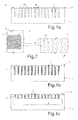
- an initial step of the manufacturing process envisages formation, within a substrate 1 of monocrystalline silicon, of a plurality of trenches 2.
- the trenches 2 are dug through a surface portion of the substrate 1 by means of known techniques of masking and anisotropic chemical etching.
- a mask 3 is formed on a top surface 1a of the substrate 1, the mask being made of a material resistant to chemical etching, for example photoresist.
- the mask 3 extends (see also the top plan view of Figure 2 ) over an area having a shape substantially corresponding to the extension of the buried area that will be subsequently obtained (as described in detail hereinafter), and has a lattice conformation, for example a honeycomb conformation.
- Figure 1a shows portions 3a of the mask 3, defining between them empty spaces 3b (the portions 3a are connected to form the aforesaid lattice).
- the trenches 2, which have vertical extension, are dug by means of markedly anisotropic chemical etching of the substrate 1, in regions corresponding to the empty spaces 3b left by the mask 3, and have, for example, a depth of from 5 ⁇ m to 500 ⁇ m.
- a deposition of silicon oxide SiO 2 or other dielectric material (such as silicon oxynitride or nitride) is carried out in such a way as to form spacers 6 on the internal lateral walls of the trenches 2 (the silicon dielectric possibly formed on the bottom of the trenches 2 is, instead, removed with an anisotropic etch).
- a step of chemical etching is carried out, for example of a TMAH type (i.e., using tetramethyl ammonium hydroxide) with characteristics of isotropy so as to form an open area 8, set underneath the trenches 2 and in fluid communication with the same trenches 2.
- the isotropic chemical etch causes digging of the portion of the substrate 1 underneath the trenches 2, both in the direction of the depth (vertical direction of extension of the trenches 2) and, to a lesser extent, in a lateral direction, transverse to the vertical direction.
- the lateral extension of the open area 8 hence corresponds substantially to the extension of the mask 3 previously formed above the substrate 1.
- the mask 3 is removed from the top surface 1a of the substrate 1, and the silicon oxide previously deposited is moreover removed, by means of a wet chemical etching.
- the spacers 6 are removed from the internal lateral walls of the trenches 2.
- a step of epitaxial growth of monocrystalline or polycrystalline silicon is carried out, preferably in deoxidizing environment (typically, in atmosphere with a high concentration of hydrogen, preferably in trichlorosilane - SiHCl 3 ), accompanied by a step of annealing, for example, in nitrogen atmosphere.
- deoxidizing environment typically, in atmosphere with a high concentration of hydrogen, preferably in trichlorosilane - SiHCl 3
- the annealing step causes a migration of the silicon atoms, which tend to move into positions of lower energy.
- a buried cavity 10 is formed within the substrate 1, altogether isolated from the external environment and contained within the substrate itself, on top of which there remains a first surface layer 12, compact and uniform, which is constituted in part by monocrystalline or polycrystalline silicon atoms grown epitaxially and in part by migrated silicon atoms, and has a thickness for example of between 2 ⁇ m and 50 ⁇ m.
- the buried cavity 10 defines, for example, a buried channel within the substrate 1, having the following dimensions: 30 ⁇ m in height (considered in the vertical direction, between a corresponding bottom wall - floor - and a top wall - roof or ceiling); 200 ⁇ m in width; 1 cm in length; the channel is located at a depth of 25 ⁇ m underneath a respective top surface 12a of the first surface layer 12, which constitutes now a surface portion of the substrate 1 in which the channel is buried.
- the buried cavity 10 can have other geometries and define further buried structures (chambers or passages), according, in particular, to the characteristics of the mask 3 used for the process of formation of the trenches 2.
- a mask is defined, having an appropriate shape (as will be clarified better hereinafter), through which an oxidation step is carried out.
- Figure 1f The structure of Figure 1f is thus obtained, in which on the top surface 12a of the first surface layer 12, in an appropriate position (as will be clarified better hereinafter), an etching mask 14 is provided (of the "hard mask” type), formed by dielectric silicon oxide and having, for example, a lattice structure defining empty spaces arranged, in the example, at a regular distance apart (along the line of cross section of Figure 1f ).
- an etching mask 14 is provided (of the "hard mask” type), formed by dielectric silicon oxide and having, for example, a lattice structure defining empty spaces arranged, in the example, at a regular distance apart (along the line of cross section of Figure 1f ).
- the process continues with a step of epitaxial deposition, following upon which a second surface layer 15 grows epitaxially on the first surface layer 12.
- the two epitaxial layers form in this step a single homogeneous region of semiconductor material, in particular monocrystalline (or polycrystalline) silicon, moreover forming with the substrate 1 a single (compact and uniform) monolithic body.
- the second surface layer 15 coats in particular the etching mask 14, which is englobed and integrated in the aforesaid homogeneous region of semiconductor material.
- the thickness of the second surface layer 15 is of 13.2 ⁇ m.
- a lithographic mask 16 is formed on a top surface 15a of the second surface layer 15, which leaves exposed a first access area 17a vertically corresponding to the etching mask 14, and possibly at least one second access area 17b, distinct from the first access area 17a.
- the etch carried out frees the structure of the etching mask 14 in such a way that it is directly suspended above the buried cavity 10, thus forming a filter element 20, made of silicon, that filters particles entering/leaving the same buried cavity 10.
- the etching mask 14 operates in fact as a shield for the etching and causes underlying portions of silicon to remain substantially intact, in effect replicating the lattice structure and conformation, in plan view, of the same etching mask 14 and consequently defining the filter element 20.
- the filter element 20 is thus formed by a lattice structure having vertical extension (with a height equal to the thickness of the first surface layer 12), defining inside it a plurality of openings 22 (or pores), such as to enable the passage of fluid and withhold, instead, undesirable particles (having dimensions not compatible with the dimensions of the openings 22) . Between adjacent openings 22 vertical walls, or laminas, are present.
- the deep etch of the silicon through the lithographic mask 16 leads to the formation of a first access duct 18a (for inlet or outlet, according to the direction of the fluid), which traverses the second surface layer 15 throughout its thickness and reaches the buried cavity 10 through the filter element 20.
- the filter element 20 is set at a distance from the top surface 15a of the second surface layer 15 equal to the thickness of the second surface layer 15, and is set between the first access duct 18a and the buried cavity 10.
- the etching step that leads to definition of the first access duct 18a in fluid communication with the buried cavity 10 leads automatically and at the same time to definition of the filter element 20 associated to the same first access duct 18a, thanks to the prior formation of the etching mask 14 in an appropriate position and with appropriate configuration; in particular, the filter element 20 is formed directly on the buried cavity 10.
- the deep etch of the silicon through the lithographic mask 16 moreover leads to formation of a second access duct 18b (for outlet or inlet of the fluid, according to the direction of the fluid and to the function of the first access duct 18a), which, starting from the top surface 15a of the second surface layer 15, traverses throughout their thickness the first and the second surface layers 12, 15 and reaches the buried cavity 10.
- the first access duct 18a can be set in a position corresponding to the inlet of a channel defined by the buried cavity 10, and the second access duct 18b in a position corresponding to the outlet of the same channel.
- the process terminates ( Figure 1j ), with a step of removal of the lithographic mask 16 from above the top surface 15a of the second surface layer 15, and moreover of the etching mask 14 from above the filter element 20, by means of respective steps of selective chemical etching.
- a micromechanical structure is hence obtained, designated as a whole by 25, including a buried cavity 10 (for example defining a channel), communicating with the external environment by means of a first access duct 18a and a second access duct 18b.
- a filter element 20 is formed, designed to enable removal of impurities and contaminants coming from outside towards the buried cavity 10, in the case where said filter element 20 is set in a position corresponding to an inlet duct, or else to enable the removal of impurities and contaminants moving from inside the buried cavity 10 towards the outside, in the case where the filter element 20 is set in a position corresponding to an outlet duct.
- the buried cavity 10 and the filter element 20 are integrated in one and the same monolithic body of semiconductor material.
- Figures 3a and 3b are schematic top plan views of two possible patterns of the filter element 20, in the case where it has openings 22 having a square shape or a cross shape, respectively (the lattice defining the same openings 22 having a corresponding shape).
- the etching mask 14 has in this case a similar shape, forming a lattice defining openings having in plan view a square shape or a cross shape, respectively. It is evident that the transverse extension of the filter element can vary according to the requirements of filtering and design of the microfluidic structure.
- the openings 22 have micrometric or sub-micrometric dimensions, with a width (in the transverse direction) for example greater than 0.5 ⁇ m and smaller than 50 ⁇ m.
- the shape and the optimal geometrical characteristics of the openings 22, and in general of the filter element 20, can in any case vary according to the impurities that are to be filtered, for example according to the dimensions or structural characteristics of the same impurities.
- the thickness of the first surface layer 12 determines the height (or thickness) of the openings 22 of the filter element 20 (and of the corresponding vertical walls or laminas), and hence, amongst other things, the filtering properties of the filter element 20.
- the thickness of the second surface layer 15 determines, instead, the height (or thickness) of the access duct in fluid communication with the filter element 20, and hence, for example, the corresponding characteristics of fluid flow-rate.
- the thickness of the second surface layer 15 determines the height of the inlet and outlet pumping cavities.
- the buried cavity 10, and the corresponding filter element 20 are provided during front-end processing steps (in particular, solely by means of etches from the front of the starting substrate of semiconductor material), without requiring back-end operations, with evident advantages in terms of reduction of the risks of contamination (both from outside and from inside) and of generation of impurities, and of simplification in the manufacturing process and reduction in the associated costs.
- the resulting micromechanical structure 25 is extremely compact, in so far as it is obtained from a single monolithic body of a same semiconductor material, with the filter element 20, the buried cavity 10, and the corresponding access ducts 18a, 18b integrated inside the body.
- the process described enables large thicknesses of the filter element 20, even in the order of tens of microns (for example, 30 ⁇ m), enabling reduction of the risk of mechanical failure, for example following upon impact or dropping.
- the presence of the filter element 20, and of the resulting micro-filtration effect affords advantages from the standpoint of the fluidic path, in so far as it prevents external particles from entering undesirable areas of the micromechanical structure (and hinder, for example moving parts, such as valves), and moreover enables maintenance of a high level of purity of the flowing fluids (in particular in the case of administration of drugs to a patient).
- Figure 4 shows an example of a microfluidic device, designated by 30, comprising the micromechanical structure 25, and in particular the substrate 1 inside which the buried cavity 10 and the filter element 20 are provided.
- the microfluidic device 30 is a micropump for administration of drugs, for example for administration of insulin to a patient.
- the manufacturing process and in particular the step of TMAH isotropic etching (see the foregoing description), can be calibrated in such a way that the buried cavity 10 defines with a bottom surface 1b of the substrate 1 (opposite to the top surface 15a) an elastic membrane 32 (i.e., a region of semiconductor material with a thickness such as to have sufficient characteristics of deformability).
- an elastic membrane 32 i.e., a region of semiconductor material with a thickness such as to have sufficient characteristics of deformability.
- the microfluidic device 30 further comprises mechanical actuators 34, shown schematically (for example straps actuated by piezoelectric elements), which are coupled to the elastic membrane 32 (externally with respect to the substrate 1) and can be actuated to cause deformation of the same elastic membrane 32, in particular with alternating movement of compression and expansion.
- This alternating movement generates a flow of the fluid contained within the buried cavity 10, starting from a corresponding inlet towards a corresponding outlet (it is to be noted that, in a way not illustrated, inlet valves and outlet valves may be present to regulate and control the directionality and the inlet/outlet of the flow of fluid with respect to the buried cavity 10, the direction of which is indicated by the arrow in Figure 4 ).
- the filter element 20, in the example shown in Figure 4 set at inlet to the buried cavity 10, is traversed by the fluid in a direction parallel to its vertical extension, and prevents external particles from clogging the fluidic channel or hindering proper opening/closing of the inlet and/or outlet valves with consequent undesirable outflow of fluid.
- the filter element 20 is traversed by the fluids at inlet in the vertical direction.
- a possible process variant can envisage formation of a pair of filter elements 20, set, with respect to the buried cavity 10, in a position corresponding both to the inlet duct and to the outlet duct.
- the number itself of the ducts for access to the buried cavity 10 can moreover differ with respect to the one illustrated.
- the buried cavity 10 can possibly be divided into a number of sections, as shown schematically in Figures 5a-5c , which can then be connected in a single channel.
- the buried cavity 10 may have a lateral connection portion, designated by 10a, communicating directly with an access duct 18a, and, for example, three sections in length, designated with 10b, connected at the lateral connection portion 10a and converging into the single channel (not illustrated).
- 10a lateral connection portion
- 10b three sections in length
- the width of the filter element 20 (in a direction transverse to that of vertical extension) can possibly be smaller than that of the corresponding inlet/outlet access duct.
- further shapes or patterns may equally be envisaged for the filter element 20, according to specific filtering requirements.
- the process described for manufacturing of the filter element 20 is advantageously applied starting from a buried cavity 10 provided within a body of semiconductor material, irrespective of the way with which the same buried cavity was previously formed; in addition, it is evident that the micromechanical structure 25 can find advantageous use in all the applications in which the presence of a buried cavity provided with a filter element in fluid communication with the same buried cavity is required.
Abstract
Description
- The present invention relates to a process for manufacturing a micromechanical structure having a buried area provided with a filter; the micromechanical structure is formed in a body made of semiconductor material, in particular silicon, using micromachining techniques and finds advantageous use, for example, for microfluidic applications.
- As is known, in the semiconductor industry micromachining techniques enable manufacturing of micromechanical or MEMS (microelectromechanical systems) structures, which have a wide range of applications.
- In particular, in the microfluidic field, it is common to manufacture structures including buried areas (for example channels, chambers, or cavities) within a silicon substrate (or other semiconductor material body), which are for example used for enabling passage of fluids, such as drugs that are to be administered to a patient or inks used for printing operations, or else for enabling even complex chemical reactions, such as reactions of multiplication of DNA sequences through the PCR (polymerase chain reaction) process.
- In general, the manufactured buried areas enable an environment to be obtained that is substantially separate and distinct from the external environment (and possibly communicates with the external environment by means of one or more access ducts), in which chemical reactions, exchanges or flows of fluids take place in a controlled manner.
- Known processes for manufacturing of microfluidic structures provided with buried areas generally envisage the use of techniques of processing from the back of the silicon substrate or wafer (or other body of semiconductor material). These processes envisage chemical etching of the back of the substrate to define a first wall, for example a top wall, of the area that is to be buried (which defines, for example, a channel or a cavity), and next bonding of the substrate with a different structural body (for example, a plate of glass or an adhesive layer), such as to close the buried area defining a corresponding second wall thereof, for example a bottom wall. These operations can be carried out, in part, during the processes for assembling the package or "moulding" of the microfluidic structures (operations known as a whole as "back-end" operations).
- In addition, ducts for access to the buried area can be provided with purposely designed etches from the front of the substrate (techniques of silicon processing known as a whole as "front-end" techniques).
- These manufacturing processes have, however, certain drawbacks that do not enable full exploitation of the characteristics thereof, amongst which:
- the techniques of back processing, and the subsequent operations of bonding between different bodies, entail generally the generation of undesirable particles and contaminants, which can jeopardize operation of the final microfluidic device; and
- the back-end and bonding operations are in general complex, costly, and generally require long processing times.
- In particular, the problem of contamination from external particles, which is not due only to the aforesaid manufacturing operations and to the residue of processing, but also to the presence for other reasons of external particles that can interact with the buried area, is particularly felt, in so far as this contamination can jeopardize the performance of the microfluidic devices or proper execution of the operations of delivery or passage of the fluids associated thereto.
- For this reason, the use of more or less complex filters has been proposed, which are designed to be coupled to at least one access duct (inlet or outlet duct) in fluid communication with the buried cavity. In particular, given that these filters have pores of micrometric or sub-micrometric dimensions, they enable filtering and subsequent removal of possible impurities during flow of the liquids.
- For example, patent No.
US 5,753,014 discloses the formation of a membrane filter by means of chemical etching of a silicon membrane having a thickness of a few microns. In particular, the membrane is obtained by means of chemical etching from the back of a silicon substrate, and a desired pattern of micrometric or sub-micrometric pores is subsequently defined through the membrane with photolithographic techniques. The membrane filter thus obtained can be coupled, as an external element, to structures with buried areas or ducts with a diameter (size) of from a few microns up to hundreds of microns or even millimetres, for operations of filtering of the incoming/outgoing fluids. - This solution is not, however, optimized from the standpoint of simplicity and economy of the manufacturing process, for example because it requires complex steps of coupling of the filter to structures formed separately, it requires to comply with specifications of mechanical and/or optical alignment, and moreover it does not enable in any case reduction of the contaminations inherent in the manufacturing process of the buried areas.
- Solutions are also known in which the filtering element is defined by bonding two bodies so as to define vertical pillars arranged according to desired lattices in a direction transverse to the direction of flow of the fluids. These solutions suffer from further disadvantages, amongst which: the process of bonding of the various bodies suffers from misalignment inaccuracy, the value of which (for example +/-20 µm) may not enable formation of sufficiently small filtering pores (for example of a diameter of 0.5 µm) ; during the bonding operation, the distance between the vertical pillars and the body facing them may not be sufficiently repeatable for enabling an adequate filtering action; and furthermore, in order to obtain adequate flows of fluids, the buried channels are required to have, for example, a height of some tens of microns (for example, a height of 50 µm) , with the consequent fragility of the aforesaid pillars that extend vertically from the bottom wall to the top wall of the channels (failure of the pillars can jeopardize the filtering action and can itself cause impurities in the flow of the fluids) .
- The aim of the present invention is to solve, either totally or partially, the problems highlighted previously, and in particular to provide a process that will enable formation, in a body of semiconductor material, of buried areas provided with structures for filtering of contaminating impurities, and that will be simple and inexpensive to implement.
- According to the present invention a process for manufacturing a micromechanical structure having a buried area provided with a filter, and a corresponding micromechanical structure, are consequently provided as defined in the annexed claims.
- For a better understanding of the present invention, a preferred embodiment thereof is now described, purely by way of non-limiting example and with reference to the attached drawings, wherein:
- -
Figures 1a-1j show schematic cross sections of a body of semiconductor material, in successive steps of a process for manufacturing a micromechanical structure including a buried area provided with a filter, according to one aspect of the present invention; - -
Figure 2 shows a schematic top plan view of a portion of the body of semiconductor material of Figure la; - -
Figures 3a and 3b show schematic top plan views of a portion of a filter of the micromechanical structure ofFigure 1j , according to respective variant embodiments; - -
Figure 4 shows a schematic cross section of a microfluidic device comprising the micromechanical structure ofFigure 1j ; - -
Figure 5a shows a schematic and simplified top plan view of a portion of the micromechanical structure, in a variant embodiment; and - -
Figures 5b and 5c show cross sections of the micromechanical structure ofFigure 5a taken along respective lines of cross section. - A manufacturing process according to one embodiment of the present invention is now described; it is to be noted that some initial steps of the manufacturing process are, at least in part, based upon the processes described in patents Nos.
EP 1 324 382 B1EP 1 577 656 B1 - As shown in
Figure 1a (not drawn to scale, as neither are the subsequent figures), an initial step of the manufacturing process envisages formation, within asubstrate 1 of monocrystalline silicon, of a plurality of trenches 2. The trenches 2 are dug through a surface portion of thesubstrate 1 by means of known techniques of masking and anisotropic chemical etching. - In particular, a
mask 3 is formed on atop surface 1a of thesubstrate 1, the mask being made of a material resistant to chemical etching, for example photoresist. - The
mask 3 extends (see also the top plan view ofFigure 2 ) over an area having a shape substantially corresponding to the extension of the buried area that will be subsequently obtained (as described in detail hereinafter), and has a lattice conformation, for example a honeycomb conformation.Figure 1a showsportions 3a of themask 3, defining between themempty spaces 3b (theportions 3a are connected to form the aforesaid lattice). - The trenches 2, which have vertical extension, are dug by means of markedly anisotropic chemical etching of the
substrate 1, in regions corresponding to theempty spaces 3b left by themask 3, and have, for example, a depth of from 5 µm to 500 µm. - Next (
Figure 1b ), once again with themask 3 positioned on thetop surface 1a of thesubstrate 1, a deposition of silicon oxide (SiO2 or other dielectric material (such as silicon oxynitride or nitride) is carried out in such a way as to formspacers 6 on the internal lateral walls of the trenches 2 (the silicon dielectric possibly formed on the bottom of the trenches 2 is, instead, removed with an anisotropic etch). - Then (
Figure 1c ), a step of chemical etching is carried out, for example of a TMAH type (i.e., using tetramethyl ammonium hydroxide) with characteristics of isotropy so as to form anopen area 8, set underneath the trenches 2 and in fluid communication with the same trenches 2. In particular, the isotropic chemical etch causes digging of the portion of thesubstrate 1 underneath the trenches 2, both in the direction of the depth (vertical direction of extension of the trenches 2) and, to a lesser extent, in a lateral direction, transverse to the vertical direction. The lateral extension of theopen area 8 hence corresponds substantially to the extension of themask 3 previously formed above thesubstrate 1. - Next (
Figure 1d ) , themask 3 is removed from thetop surface 1a of thesubstrate 1, and the silicon oxide previously deposited is moreover removed, by means of a wet chemical etching. In particular, in this step, thespacers 6 are removed from the internal lateral walls of the trenches 2. - Then (
Figure 1e ), a step of epitaxial growth of monocrystalline or polycrystalline silicon is carried out, preferably in deoxidizing environment (typically, in atmosphere with a high concentration of hydrogen, preferably in trichlorosilane - SiHCl3), accompanied by a step of annealing, for example, in nitrogen atmosphere. As discussed in detail in the aforementioned European patents, the annealing step causes a migration of the silicon atoms, which tend to move into positions of lower energy. - Consequently, and also thanks to the short distance between the trenches 2, following upon this step, a buried
cavity 10 is formed within thesubstrate 1, altogether isolated from the external environment and contained within the substrate itself, on top of which there remains afirst surface layer 12, compact and uniform, which is constituted in part by monocrystalline or polycrystalline silicon atoms grown epitaxially and in part by migrated silicon atoms, and has a thickness for example of between 2 µm and 50 µm. - The
buried cavity 10 defines, for example, a buried channel within thesubstrate 1, having the following dimensions: 30 µm in height (considered in the vertical direction, between a corresponding bottom wall - floor - and a top wall - roof or ceiling); 200 µm in width; 1 cm in length; the channel is located at a depth of 25 µm underneath a respectivetop surface 12a of thefirst surface layer 12, which constitutes now a surface portion of thesubstrate 1 in which the channel is buried. - Clearly, the buried
cavity 10 can have other geometries and define further buried structures (chambers or passages), according, in particular, to the characteristics of themask 3 used for the process of formation of the trenches 2. - Next, according to a peculiar aspect of the present invention, on the
top surface 12a of thefirst surface layer 12 a mask is defined, having an appropriate shape (as will be clarified better hereinafter), through which an oxidation step is carried out. - The structure of
Figure 1f is thus obtained, in which on thetop surface 12a of thefirst surface layer 12, in an appropriate position (as will be clarified better hereinafter), anetching mask 14 is provided (of the "hard mask" type), formed by dielectric silicon oxide and having, for example, a lattice structure defining empty spaces arranged, in the example, at a regular distance apart (along the line of cross section ofFigure 1f ). - Then, as shown in
Figure 1g , the process continues with a step of epitaxial deposition, following upon which asecond surface layer 15 grows epitaxially on thefirst surface layer 12. The two epitaxial layers form in this step a single homogeneous region of semiconductor material, in particular monocrystalline (or polycrystalline) silicon, moreover forming with thesubstrate 1 a single (compact and uniform) monolithic body. Thesecond surface layer 15 coats in particular theetching mask 14, which is englobed and integrated in the aforesaid homogeneous region of semiconductor material. For example, the thickness of thesecond surface layer 15 is of 13.2 µm. - Next (
Figure 1h ), alithographic mask 16 is formed on atop surface 15a of thesecond surface layer 15, which leaves exposed afirst access area 17a vertically corresponding to theetching mask 14, and possibly at least onesecond access area 17b, distinct from thefirst access area 17a. - There is then carried out (
Figure 1i ) a step of deep etching of the silicon, with characteristics of anisotropy and a depth of etching such as to involve the entire thicknesses of the first andsecond surface layers cavity 10. - In particular, the etch carried out frees the structure of the
etching mask 14 in such a way that it is directly suspended above the buriedcavity 10, thus forming afilter element 20, made of silicon, that filters particles entering/leaving the same buriedcavity 10. - The
etching mask 14 operates in fact as a shield for the etching and causes underlying portions of silicon to remain substantially intact, in effect replicating the lattice structure and conformation, in plan view, of thesame etching mask 14 and consequently defining thefilter element 20. Thefilter element 20 is thus formed by a lattice structure having vertical extension (with a height equal to the thickness of the first surface layer 12), defining inside it a plurality of openings 22 (or pores), such as to enable the passage of fluid and withhold, instead, undesirable particles (having dimensions not compatible with the dimensions of the openings 22) . Betweenadjacent openings 22 vertical walls, or laminas, are present. - In particular, the deep etch of the silicon through the
lithographic mask 16 leads to the formation of afirst access duct 18a (for inlet or outlet, according to the direction of the fluid), which traverses thesecond surface layer 15 throughout its thickness and reaches the buriedcavity 10 through thefilter element 20. Thefilter element 20 is set at a distance from thetop surface 15a of thesecond surface layer 15 equal to the thickness of thesecond surface layer 15, and is set between thefirst access duct 18a and the buriedcavity 10. - It is hence emphasized that the etching step that leads to definition of the
first access duct 18a in fluid communication with the buriedcavity 10 leads automatically and at the same time to definition of thefilter element 20 associated to the samefirst access duct 18a, thanks to the prior formation of theetching mask 14 in an appropriate position and with appropriate configuration; in particular, thefilter element 20 is formed directly on the buriedcavity 10. - The deep etch of the silicon through the
lithographic mask 16 moreover leads to formation of asecond access duct 18b (for outlet or inlet of the fluid, according to the direction of the fluid and to the function of thefirst access duct 18a), which, starting from thetop surface 15a of thesecond surface layer 15, traverses throughout their thickness the first and thesecond surface layers cavity 10. For example, thefirst access duct 18a can be set in a position corresponding to the inlet of a channel defined by the buriedcavity 10, and thesecond access duct 18b in a position corresponding to the outlet of the same channel. - The process terminates (
Figure 1j ), with a step of removal of thelithographic mask 16 from above thetop surface 15a of thesecond surface layer 15, and moreover of theetching mask 14 from above thefilter element 20, by means of respective steps of selective chemical etching. - At the end of these steps of removal, the formation of a micromechanical structure is hence obtained, designated as a whole by 25, including a buried cavity 10 (for example defining a channel), communicating with the external environment by means of a
first access duct 18a and asecond access duct 18b. Using the same process steps, in themicromechanical structure 25, afilter element 20 is formed, designed to enable removal of impurities and contaminants coming from outside towards the buriedcavity 10, in the case where saidfilter element 20 is set in a position corresponding to an inlet duct, or else to enable the removal of impurities and contaminants moving from inside the buriedcavity 10 towards the outside, in the case where thefilter element 20 is set in a position corresponding to an outlet duct. The buriedcavity 10 and thefilter element 20 are integrated in one and the same monolithic body of semiconductor material. - It is moreover emphasized that:
- the pattern of the
etching mask 14 brings about, once the process is completed, the corresponding filtering pattern of thefilter element 20; and - the arrangement of the
etching mask 14 itself with respect to the buriedcavity 10 determines the corresponding position of thefilter element 20, and, hence, its function with respect to filtering of the impurities coming from the outside towards the buriedcavity 10, or moving from the buriedcavity 10 itself towards the outside. -
Figures 3a and 3b are schematic top plan views of two possible patterns of thefilter element 20, in the case where it hasopenings 22 having a square shape or a cross shape, respectively (the lattice defining thesame openings 22 having a corresponding shape). As it is clear, theetching mask 14 has in this case a similar shape, forming a lattice defining openings having in plan view a square shape or a cross shape, respectively. It is evident that the transverse extension of the filter element can vary according to the requirements of filtering and design of the microfluidic structure. - In particular, the
openings 22 have micrometric or sub-micrometric dimensions, with a width (in the transverse direction) for example greater than 0.5 µm and smaller than 50 µm. In a per-se known manner, the shape and the optimal geometrical characteristics of theopenings 22, and in general of thefilter element 20, can in any case vary according to the impurities that are to be filtered, for example according to the dimensions or structural characteristics of the same impurities. - As previously indicated, the thickness of the
first surface layer 12 determines the height (or thickness) of theopenings 22 of the filter element 20 (and of the corresponding vertical walls or laminas), and hence, amongst other things, the filtering properties of thefilter element 20. The thickness of thesecond surface layer 15 determines, instead, the height (or thickness) of the access duct in fluid communication with thefilter element 20, and hence, for example, the corresponding characteristics of fluid flow-rate. - For example, in the case where the
micromechanical structure 25 constitutes a micropump (as described in detail hereinafter), the thickness of thesecond surface layer 15 determines the height of the inlet and outlet pumping cavities. - The advantages of the manufacturing process according to the present invention are clear from the foregoing description.
- It is emphasized in any case that the buried
cavity 10, and thecorresponding filter element 20, are provided during front-end processing steps (in particular, solely by means of etches from the front of the starting substrate of semiconductor material), without requiring back-end operations, with evident advantages in terms of reduction of the risks of contamination (both from outside and from inside) and of generation of impurities, and of simplification in the manufacturing process and reduction in the associated costs. - The resulting
micromechanical structure 25 is extremely compact, in so far as it is obtained from a single monolithic body of a same semiconductor material, with thefilter element 20, the buriedcavity 10, and thecorresponding access ducts - In particular, the process described enables large thicknesses of the
filter element 20, even in the order of tens of microns (for example, 30 µm), enabling reduction of the risk of mechanical failure, for example following upon impact or dropping. - In general, the presence of the
filter element 20, and of the resulting micro-filtration effect, affords advantages from the standpoint of the fluidic path, in so far as it prevents external particles from entering undesirable areas of the micromechanical structure (and hinder, for example moving parts, such as valves), and moreover enables maintenance of a high level of purity of the flowing fluids (in particular in the case of administration of drugs to a patient). - In addition, it is advantageous the arrangement of the filter element 20 (and in particular of the corresponding vertical walls) parallel to the direction of flow of the fluids at inlet/outlet to/from the buried
cavity 10. - The aforesaid characteristics render advantageous the use of the process described, and of the corresponding
micromechanical structure 25, in a very wide range of applications. - For example,
Figure 4 shows an example of a microfluidic device, designated by 30, comprising themicromechanical structure 25, and in particular thesubstrate 1 inside which the buriedcavity 10 and thefilter element 20 are provided. - In the specific case, the
microfluidic device 30 is a micropump for administration of drugs, for example for administration of insulin to a patient. - In this case, the manufacturing process, and in particular the step of TMAH isotropic etching (see the foregoing description), can be calibrated in such a way that the buried
cavity 10 defines with abottom surface 1b of the substrate 1 (opposite to thetop surface 15a) an elastic membrane 32 (i.e., a region of semiconductor material with a thickness such as to have sufficient characteristics of deformability). - The
microfluidic device 30 further comprisesmechanical actuators 34, shown schematically (for example straps actuated by piezoelectric elements), which are coupled to the elastic membrane 32 (externally with respect to the substrate 1) and can be actuated to cause deformation of the sameelastic membrane 32, in particular with alternating movement of compression and expansion. This alternating movement generates a flow of the fluid contained within the buriedcavity 10, starting from a corresponding inlet towards a corresponding outlet (it is to be noted that, in a way not illustrated, inlet valves and outlet valves may be present to regulate and control the directionality and the inlet/outlet of the flow of fluid with respect to the buriedcavity 10, the direction of which is indicated by the arrow inFigure 4 ). Thefilter element 20, in the example shown inFigure 4 set at inlet to the buriedcavity 10, is traversed by the fluid in a direction parallel to its vertical extension, and prevents external particles from clogging the fluidic channel or hindering proper opening/closing of the inlet and/or outlet valves with consequent undesirable outflow of fluid. In particular, in the case illustrated, thefilter element 20 is traversed by the fluids at inlet in the vertical direction. - Finally, it is clear that modifications and variations may be made to what has been described and illustrated herein, without thereby departing from the scope of the present invention, as defined in the annexed claims.
- For example, a possible process variant (not illustrated) can envisage formation of a pair of
filter elements 20, set, with respect to the buriedcavity 10, in a position corresponding both to the inlet duct and to the outlet duct. The number itself of the ducts for access to the buriedcavity 10 can moreover differ with respect to the one illustrated. - In the case of channel formation, the buried
cavity 10 can possibly be divided into a number of sections, as shown schematically inFigures 5a-5c , which can then be connected in a single channel. In this case, the buriedcavity 10 may have a lateral connection portion, designated by 10a, communicating directly with anaccess duct 18a, and, for example, three sections in length, designated with 10b, connected at thelateral connection portion 10a and converging into the single channel (not illustrated). This solution can be advantageous for preventing problems of formation of mechanical stresses and for distributing the pressures that may possibly be generated on the entiremicromechanical structure 25. - The width of the filter element 20 (in a direction transverse to that of vertical extension) can possibly be smaller than that of the corresponding inlet/outlet access duct. Clearly, further shapes or patterns may equally be envisaged for the
filter element 20, according to specific filtering requirements. - Finally, it is evident that the process described for manufacturing of the
filter element 20 is advantageously applied starting from a buriedcavity 10 provided within a body of semiconductor material, irrespective of the way with which the same buried cavity was previously formed; in addition, it is evident that themicromechanical structure 25 can find advantageous use in all the applications in which the presence of a buried cavity provided with a filter element in fluid communication with the same buried cavity is required.
Claims (17)
- A process for manufacturing a micromechanical structure (25), comprising the steps of:- forming a buried cavity (10) within a body (1, 12) of semiconductor material, having a top surface (12a), said buried cavity (10) being separated from said top surface (12a) by a first surface layer (12) of said body; and- forming a first access duct (18a) designed to enable fluid communication between said buried cavity (10) and an environment external to said body,
characterized by comprising the steps of:- forming an etching mask (14) on said top surface (12a) at a first access area (17a);- forming a second surface layer (15) on said top surface (12a) and said etching mask (14);- carrying out an etching operation such as to remove, at said first access area (17a), a portion of said second surface layer (15), and an underlying portion of said first surface layer (12) not covered by said etching mask (14) until said buried cavity (10) is reached, said etching operation thus forming both said first access duct (18a) and a filter element (20), set between said first access duct (18a) and said buried cavity (10) and formed by a remaining portion of said first surface layer (12) covered by said etching mask (14). - The process according to claim 1, wherein said etching mask (14) has a lattice structure (3a) defining a plurality of openings (3b) having sub-micrometric or micrometric dimensions.
- The process according to claim 1 or 2, wherein said etching mask (14) is of a "hard mask" type.
- The process according to any one of the preceding claims, wherein said step of forming a second surface layer (15) comprises growing epitaxially said second surface layer (15) on said top surface (12a) of said first surface layer (12); said second surface layer (15) and said body (1, 12) forming a single monolithic structure of semiconductor material.
- The process according to claim 4, wherein said filter element (20) is integrated within said monolithic structure, at a given distance from a respective top surface (15a) of said second surface layer (15), said given distance being equal to the thickness of said second surface layer (15); wherein said thickness of said second surface layer (15) moreover defines a height of said first access duct (18a).
- The process according to claim 4 or 5, wherein said semiconductor material is monocrystalline or polycrystalline silicon, and said etching mask (14) is made of silicon oxide or silicon dielectric.
- The process according to any one of the preceding claims, further comprising the step of removing said etching mask (14) at the end of said etching operation.
- The process according to any one of the preceding claims, wherein said etching operation is carried out through a lithographic mask (16) formed on a respective top surface (15a) of said second surface layer (15), said lithographic mask (16) having a first opening in a position corresponding to said first access area (17a).
- The process according to claim 8, wherein said lithographic mask (16) has a second opening in a position corresponding to a second access area (17b); and wherein said etching operation is further configured so as to remove, at said second access area (17b), a portion of said second surface layer (15) and an underlying portion of said first surface layer (12) until said buried cavity (10) is reached, thus forming a second access duct (18b), designed to enable fluid communication between said buried cavity (10) and said external environment.
- The process according to claim 9, wherein said first access duct (18a) is an inlet/outlet duct for introduction/ extraction of fluid into/from said buried cavity (10), and said second access duct (18b) is an outlet/inlet duct for said fluid.
- The process according to any one of the preceding claims, wherein said step of forming a buried cavity (10) comprises the steps of:- digging trenches (2) within a surface portion of a substrate (1) of semiconductor material;- carrying out chemical etching through said trenches (2) to form an open area (8) in said substrate (1) underneath said trenches (2) and in fluid communication with said trenches (2);- growing epitaxially, on said surface portion of said substrate (1) said first surface layer (12), which forms with said substrate (1) said body (1, 12) of semiconductor material and closes at the top said trenches (2) and said open area (8) with respect to said external environment; and- carrying out a step of annealing of said body (1, 12).
- A micromechanical structure (25) comprising:- a monolithic body (1, 12, 15) of semiconductor material, having a top surface (15a) and including within it a buried cavity (10), said buried cavity (10) being separated from said top surface (15a) by a surface layer (12, 15) of said monolithic body; and- a first access duct (18a) designed to enable fluid communication between said buried cavity (10) and an environment external to said monolithic body,
characterized by comprising:- a filter element (20) set between said first access duct (18a) and said buried cavity (10), said filter element (20) being integrated within said monolithic body and being set at a given distance from said top surface (15a). - The structure according to claim 12, wherein said filter element (20) extends through a first portion (12) of said surface layer (12, 15), set in contact with said buried cavity (10); and wherein said first access duct (18a) extends through a second portion (15) of said surface layer (12, 15), which is contiguous to said first portion (12) , is set in contact with said top surface (15a), and has a thickness equal to said given distance.
- The structure according to claim 12 or 13, further comprising a second access duct (18b) designed to enable fluid communication between said buried cavity (10) and said external environment; said second access duct (18b) extending throughout a thickness of said surface layer (12, 15), starting from said buried cavity (10) up to said top surface (15a).
- The structure according to any one of claims 12-14, wherein said filter element (20) has a lattice structure defining a plurality of openings (22) having sub-micrometric or micrometric dimensions.
- A microfluidic device (30) comprising a micromechanical structure (25) according to any one of claims 12-15, configured to implement a micropump for fluids.
- The device according to claim 16, wherein said monolithic body (1, 12, 15) further has a bottom surface (1b), opposite to said top surface (15a), and a membrane (32) set between said bottom surface (1b) and said buried cavity (10); further comprising actuator means (34) that can be actuated to cause a deformation of said membrane (32) such as to generate a flow of fluid within said buried cavity (10).
Applications Claiming Priority (1)
| Application Number | Priority Date | Filing Date | Title |
|---|---|---|---|
| ITTO20100641 | 2010-07-26 |
Publications (2)
| Publication Number | Publication Date |
|---|---|
| EP2412665A1 true EP2412665A1 (en) | 2012-02-01 |
| EP2412665B1 EP2412665B1 (en) | 2013-06-19 |
Family
ID=43740026
Family Applications (1)
| Application Number | Title | Priority Date | Filing Date |
|---|---|---|---|
| EP11175428.9A Not-in-force EP2412665B1 (en) | 2010-07-26 | 2011-07-26 | Process for manufacturing a micromechanical structure having a buried area provided with a filter |
Country Status (3)
| Country | Link |
|---|---|
| US (2) | US8633553B2 (en) |
| EP (1) | EP2412665B1 (en) |
| CN (1) | CN102344111B (en) |
Families Citing this family (18)
| Publication number | Priority date | Publication date | Assignee | Title |
|---|---|---|---|---|
| US8633553B2 (en) | 2010-07-26 | 2014-01-21 | Stmicroelectronics S.R.L. | Process for manufacturing a micromechanical structure having a buried area provided with a filter |
| US9102519B2 (en) * | 2013-03-14 | 2015-08-11 | Infineon Technologies Ag | Semiconductor devices and methods of forming thereof |
| DE102014224063B3 (en) * | 2014-11-26 | 2016-03-17 | Robert Bosch Gmbh | MEMS device with a deformable membrane |
| CN105390475A (en) * | 2015-10-20 | 2016-03-09 | 北京大学 | Capacitor integration structure inside substrate, and manufacturing method thereof |
| ITUB20155716A1 (en) * | 2015-11-19 | 2017-05-19 | St Microelectronics Srl | MICRO-ELECTRO-MECHANICAL DEVICE EQUIPPED WITH TWO CAVITIES AND RELATIVE PROCESS OF MANUFACTURE |
| US9731965B1 (en) | 2016-03-31 | 2017-08-15 | Stmicroelectronics S.R.L. | Dry scribing methods, devices and systems |
| WO2018013136A1 (en) * | 2016-07-15 | 2018-01-18 | Hewlett-Packard Development Company, L.P. | Plurality of filters |
| IT201700034134A1 (en) | 2017-03-28 | 2018-09-28 | St Microelectronics Srl | FLUID-RELEASE DEVICE WITH CROSSTALK REDUCTION ELEMENT, PRINT HEAD INCLUDING THE EJECTION DEVICE, PRINTER INCLUDING THE PRINT HEAD AND PROCESS OF MANUFACTURING THE EJECTION DEVICE |
| IT201700124348A1 (en) * | 2017-10-31 | 2019-05-01 | St Microelectronics Srl | MEMIE DEVICE OF PIEZOELECTRIC TYPE WITH SUSPENDED MEMBRANE AND ITS MANUFACTURING PROCESS |
| IT201800001152A1 (en) | 2018-01-17 | 2019-07-17 | St Microelectronics Srl | MANUFACTURING METHOD OF A FLUID EJECTION DEVICE WITH IMPROVED RESONANCE FREQUENCY AND FLUID EJECTION SPEED, AND FLUID EJECTION DEVICE |
| US10974508B2 (en) | 2018-04-27 | 2021-04-13 | Stmicroelectronics S.R.L. | Fluid ejection device with piezoelectric actuator and manufacturing process thereof |
| IT201800005824A1 (en) | 2018-05-29 | 2019-11-29 | MEMS MICROFLUIDIC DEVICE FOR THE EXPULSION OF FLUIDS EQUIPPED WITH PIEZOELECTRIC ACTUATION AND WITH REDUCED SWELLING EFFECT | |
| US11865581B2 (en) | 2018-11-21 | 2024-01-09 | Stmicroelectronics S.R.L. | Ultrasonic MEMS acoustic transducer with reduced stress sensitivity and manufacturing process thereof |
| US11818957B2 (en) | 2019-01-21 | 2023-11-14 | Stmicroelectronics S.R.L. | Piezoelectrically actuated MEMS optical device having a protected chamber and manufacturing process thereof |
| IT201900005808A1 (en) | 2019-04-15 | 2020-10-15 | St Microelectronics Srl | MICROPUMP MEMS DEVICE FOR HANDLING OR EJECTION OF A FLUID, IN PARTICULAR MICROSOFT OR FLOWMETER |
| US10899604B2 (en) * | 2019-04-18 | 2021-01-26 | Infineon Technologies Ag | Integration of stress decoupling and particle filter on a single wafer or in combination with a waferlevel package |
| WO2020248004A1 (en) * | 2019-06-14 | 2020-12-17 | University Of South Australia | Slurry taster |
| DE102020211554B3 (en) | 2020-09-15 | 2021-09-30 | Robert Bosch Gesellschaft mit beschränkter Haftung | Manufacturing process for a micromechanical component |
Citations (6)
| Publication number | Priority date | Publication date | Assignee | Title |
|---|---|---|---|---|
| US5753014A (en) | 1993-11-12 | 1998-05-19 | Van Rijn; Cornelis Johannes Maria | Membrane filter and a method of manufacturing the same as well as a membrane |
| US20030150791A1 (en) * | 2002-02-13 | 2003-08-14 | Cho Steven T. | Micro-fluidic anti-microbial filter |
| EP1614467A2 (en) * | 2004-06-30 | 2006-01-11 | STMicroelectronics, Inc. | Method of forming buried channels and microfluidic devices having the same |
| EP1324382B1 (en) | 2001-12-28 | 2007-03-07 | STMicroelectronics S.r.l. | Process for manufacturing an SOI wafer by annealing and oxidation of buried channels |
| DE102007019647A1 (en) * | 2007-04-26 | 2008-10-30 | Robert Bosch Gmbh | Method for producing a micromechanical device with a filling layer and mask layer |
| EP1577656B1 (en) | 2004-03-19 | 2010-06-09 | STMicroelectronics Srl | Method for manufacturing a semiconductor pressure sensor |
Family Cites Families (9)
| Publication number | Priority date | Publication date | Assignee | Title |
|---|---|---|---|---|
| SE8801299L (en) * | 1988-04-08 | 1989-10-09 | Bertil Hoeoek | MICROMECHANICAL ONE-WAY VALVE |
| US20030168396A1 (en) * | 1999-12-08 | 2003-09-11 | Jacobson James D. | Monolithic filter body and fabrication technique |
| EP1123739B1 (en) * | 2000-02-11 | 2006-11-29 | STMicroelectronics S.r.l. | Integrated device for microfluid thermoregulation, and manufacturing process thereof |
| US7294536B2 (en) | 2000-07-25 | 2007-11-13 | Stmicroelectronics S.R.L. | Process for manufacturing an SOI wafer by annealing and oxidation of buried channels |
| US7227433B2 (en) * | 2004-03-31 | 2007-06-05 | Intel Corporation | Electro mechanical device having a sealed cavity |
| CA2606440A1 (en) * | 2005-04-29 | 2006-11-09 | University Of Rochester | Ultrathin porous nanoscale membranes, methods of making, and uses thereof |
| US7394148B2 (en) | 2005-06-20 | 2008-07-01 | Stats Chippac Ltd. | Module having stacked chip scale semiconductor packages |
| EP1770055B1 (en) * | 2005-09-28 | 2008-05-28 | STMicroelectronics S.r.l. | Process for manufacturing thick suspended structures of semiconductor material |
| US8633553B2 (en) | 2010-07-26 | 2014-01-21 | Stmicroelectronics S.R.L. | Process for manufacturing a micromechanical structure having a buried area provided with a filter |
-
2011
- 2011-07-25 US US13/190,254 patent/US8633553B2/en not_active Expired - Fee Related
- 2011-07-26 EP EP11175428.9A patent/EP2412665B1/en not_active Not-in-force
- 2011-07-26 CN CN201110212573.7A patent/CN102344111B/en not_active Expired - Fee Related
-
2013
- 2013-12-18 US US14/133,290 patent/US9061248B1/en not_active Expired - Fee Related
Patent Citations (6)
| Publication number | Priority date | Publication date | Assignee | Title |
|---|---|---|---|---|
| US5753014A (en) | 1993-11-12 | 1998-05-19 | Van Rijn; Cornelis Johannes Maria | Membrane filter and a method of manufacturing the same as well as a membrane |
| EP1324382B1 (en) | 2001-12-28 | 2007-03-07 | STMicroelectronics S.r.l. | Process for manufacturing an SOI wafer by annealing and oxidation of buried channels |
| US20030150791A1 (en) * | 2002-02-13 | 2003-08-14 | Cho Steven T. | Micro-fluidic anti-microbial filter |
| EP1577656B1 (en) | 2004-03-19 | 2010-06-09 | STMicroelectronics Srl | Method for manufacturing a semiconductor pressure sensor |
| EP1614467A2 (en) * | 2004-06-30 | 2006-01-11 | STMicroelectronics, Inc. | Method of forming buried channels and microfluidic devices having the same |
| DE102007019647A1 (en) * | 2007-04-26 | 2008-10-30 | Robert Bosch Gmbh | Method for producing a micromechanical device with a filling layer and mask layer |
Also Published As
| Publication number | Publication date |
|---|---|
| EP2412665B1 (en) | 2013-06-19 |
| US9061248B1 (en) | 2015-06-23 |
| US20150175410A1 (en) | 2015-06-25 |
| CN102344111B (en) | 2016-01-13 |
| US20120018819A1 (en) | 2012-01-26 |
| CN102344111A (en) | 2012-02-08 |
| US8633553B2 (en) | 2014-01-21 |
Similar Documents
| Publication | Publication Date | Title |
|---|---|---|
| EP2412665B1 (en) | Process for manufacturing a micromechanical structure having a buried area provided with a filter | |
| EP1043770B1 (en) | Formation of buried cavities in a monocrystalline semiconductor wafer and a wafer | |
| US6462391B1 (en) | Suspended moving channels and channel actuators for microfluidic applications and method for making | |
| US6787052B1 (en) | Method for fabricating microstructures with deep anisotropic etching of thick silicon wafers | |
| US10493758B2 (en) | Fluid ejection device and printhead | |
| US7226540B2 (en) | MEMS filter module | |
| EP2700614B1 (en) | Methods for fabricating MEMS structures by etching sacrificial features embedded in glass | |
| EP1308196A1 (en) | Integrated micromachined filter systems and methods | |
| EP1296067B1 (en) | Passive microvalve | |
| US20110031567A1 (en) | Process for manufacturing mems devices having buried cavities and mems device obtained thereby | |
| CN105659013B (en) | The manufacturing method of microvalve device and microvalve device | |
| US7928520B2 (en) | Micro-fluidic structure | |
| CN111828645B (en) | Membrane microfluidic valve with piezoelectric actuation and method of making same | |
| EP1845060A1 (en) | Comb structure fabrication methods and systems | |
| IT201800005778A1 (en) | MICRO-FLUID DEVICE FOR THE EXPULSION OF FLUIDS, IN PARTICULAR FOR INK PRINTING, AND RELATED MANUFACTURING PROCEDURE | |
| EP3726056B1 (en) | Micropump mems device for moving or ejecting a fluid, in particular microblower or flowmeter | |
| EP1427011B1 (en) | Method for realizing microchannels in an integrated structure | |
| US7354522B2 (en) | Substrate etching method for forming connected features | |
| CN112520687A (en) | Method for producing a micromechanical system and micromechanical system | |
| WO2012050420A1 (en) | Multilayer microfluidic filter and the method of fabricating thereof |
Legal Events
| Date | Code | Title | Description |
|---|---|---|---|
| AK | Designated contracting states |
Kind code of ref document: A1 Designated state(s): AL AT BE BG CH CY CZ DE DK EE ES FI FR GB GR HR HU IE IS IT LI LT LU LV MC MK MT NL NO PL PT RO RS SE SI SK SM TR |
|
| AX | Request for extension of the european patent |
Extension state: BA ME |
|
| PUAI | Public reference made under article 153(3) epc to a published international application that has entered the european phase |
Free format text: ORIGINAL CODE: 0009012 |
|
| RAP1 | Party data changed (applicant data changed or rights of an application transferred) |
Owner name: STMICROELECTRONICS SRL |
|
| 17P | Request for examination filed |
Effective date: 20120801 |
|
| GRAP | Despatch of communication of intention to grant a patent |
Free format text: ORIGINAL CODE: EPIDOSNIGR1 |
|
| RIC1 | Information provided on ipc code assigned before grant |
Ipc: B01L 3/00 20060101ALI20121210BHEP Ipc: B01D 71/02 20060101ALI20121210BHEP Ipc: B01D 67/00 20060101ALI20121210BHEP Ipc: B81C 1/00 20060101AFI20121210BHEP Ipc: G03F 7/00 20060101ALI20121210BHEP Ipc: F04B 19/00 20060101ALI20121210BHEP |
|
| GRAS | Grant fee paid |
Free format text: ORIGINAL CODE: EPIDOSNIGR3 |
|
| GRAA | (expected) grant |
Free format text: ORIGINAL CODE: 0009210 |
|
| AK | Designated contracting states |
Kind code of ref document: B1 Designated state(s): AL AT BE BG CH CY CZ DE DK EE ES FI FR GB GR HR HU IE IS IT LI LT LU LV MC MK MT NL NO PL PT RO RS SE SI SK SM TR |
|
| REG | Reference to a national code |
Ref country code: GB Ref legal event code: FG4D |
|
| REG | Reference to a national code |
Ref country code: CH Ref legal event code: EP |
|
| REG | Reference to a national code |
Ref country code: AT Ref legal event code: REF Ref document number: 617549 Country of ref document: AT Kind code of ref document: T Effective date: 20130715 |
|
| REG | Reference to a national code |
Ref country code: IE Ref legal event code: FG4D |
|
| REG | Reference to a national code |
Ref country code: DE Ref legal event code: R096 Ref document number: 602011002061 Country of ref document: DE Effective date: 20130814 |
|
| PG25 | Lapsed in a contracting state [announced via postgrant information from national office to epo] |
Ref country code: ES Free format text: LAPSE BECAUSE OF FAILURE TO SUBMIT A TRANSLATION OF THE DESCRIPTION OR TO PAY THE FEE WITHIN THE PRESCRIBED TIME-LIMIT Effective date: 20130930 Ref country code: FI Free format text: LAPSE BECAUSE OF FAILURE TO SUBMIT A TRANSLATION OF THE DESCRIPTION OR TO PAY THE FEE WITHIN THE PRESCRIBED TIME-LIMIT Effective date: 20130619 Ref country code: SI Free format text: LAPSE BECAUSE OF FAILURE TO SUBMIT A TRANSLATION OF THE DESCRIPTION OR TO PAY THE FEE WITHIN THE PRESCRIBED TIME-LIMIT Effective date: 20130619 Ref country code: NO Free format text: LAPSE BECAUSE OF FAILURE TO SUBMIT A TRANSLATION OF THE DESCRIPTION OR TO PAY THE FEE WITHIN THE PRESCRIBED TIME-LIMIT Effective date: 20130919 Ref country code: LT Free format text: LAPSE BECAUSE OF FAILURE TO SUBMIT A TRANSLATION OF THE DESCRIPTION OR TO PAY THE FEE WITHIN THE PRESCRIBED TIME-LIMIT Effective date: 20130619 Ref country code: GR Free format text: LAPSE BECAUSE OF FAILURE TO SUBMIT A TRANSLATION OF THE DESCRIPTION OR TO PAY THE FEE WITHIN THE PRESCRIBED TIME-LIMIT Effective date: 20130920 Ref country code: SE Free format text: LAPSE BECAUSE OF FAILURE TO SUBMIT A TRANSLATION OF THE DESCRIPTION OR TO PAY THE FEE WITHIN THE PRESCRIBED TIME-LIMIT Effective date: 20130619 |
|
| REG | Reference to a national code |
Ref country code: AT Ref legal event code: MK05 Ref document number: 617549 Country of ref document: AT Kind code of ref document: T Effective date: 20130619 |
|
| REG | Reference to a national code |
Ref country code: LT Ref legal event code: MG4D |
|
| PG25 | Lapsed in a contracting state [announced via postgrant information from national office to epo] |
Ref country code: BG Free format text: LAPSE BECAUSE OF FAILURE TO SUBMIT A TRANSLATION OF THE DESCRIPTION OR TO PAY THE FEE WITHIN THE PRESCRIBED TIME-LIMIT Effective date: 20130919 Ref country code: HR Free format text: LAPSE BECAUSE OF FAILURE TO SUBMIT A TRANSLATION OF THE DESCRIPTION OR TO PAY THE FEE WITHIN THE PRESCRIBED TIME-LIMIT Effective date: 20130619 Ref country code: RS Free format text: LAPSE BECAUSE OF FAILURE TO SUBMIT A TRANSLATION OF THE DESCRIPTION OR TO PAY THE FEE WITHIN THE PRESCRIBED TIME-LIMIT Effective date: 20130619 |
|
| REG | Reference to a national code |
Ref country code: NL Ref legal event code: VDEP Effective date: 20130619 |
|
| PG25 | Lapsed in a contracting state [announced via postgrant information from national office to epo] |
Ref country code: LV Free format text: LAPSE BECAUSE OF FAILURE TO SUBMIT A TRANSLATION OF THE DESCRIPTION OR TO PAY THE FEE WITHIN THE PRESCRIBED TIME-LIMIT Effective date: 20130619 |
|
| PG25 | Lapsed in a contracting state [announced via postgrant information from national office to epo] |
Ref country code: PT Free format text: LAPSE BECAUSE OF FAILURE TO SUBMIT A TRANSLATION OF THE DESCRIPTION OR TO PAY THE FEE WITHIN THE PRESCRIBED TIME-LIMIT Effective date: 20131021 Ref country code: CY Free format text: LAPSE BECAUSE OF FAILURE TO SUBMIT A TRANSLATION OF THE DESCRIPTION OR TO PAY THE FEE WITHIN THE PRESCRIBED TIME-LIMIT Effective date: 20130807 Ref country code: AT Free format text: LAPSE BECAUSE OF FAILURE TO SUBMIT A TRANSLATION OF THE DESCRIPTION OR TO PAY THE FEE WITHIN THE PRESCRIBED TIME-LIMIT Effective date: 20130619 Ref country code: CZ Free format text: LAPSE BECAUSE OF FAILURE TO SUBMIT A TRANSLATION OF THE DESCRIPTION OR TO PAY THE FEE WITHIN THE PRESCRIBED TIME-LIMIT Effective date: 20130619 Ref country code: EE Free format text: LAPSE BECAUSE OF FAILURE TO SUBMIT A TRANSLATION OF THE DESCRIPTION OR TO PAY THE FEE WITHIN THE PRESCRIBED TIME-LIMIT Effective date: 20130619 Ref country code: SK Free format text: LAPSE BECAUSE OF FAILURE TO SUBMIT A TRANSLATION OF THE DESCRIPTION OR TO PAY THE FEE WITHIN THE PRESCRIBED TIME-LIMIT Effective date: 20130619 Ref country code: BE Free format text: LAPSE BECAUSE OF FAILURE TO SUBMIT A TRANSLATION OF THE DESCRIPTION OR TO PAY THE FEE WITHIN THE PRESCRIBED TIME-LIMIT Effective date: 20130619 Ref country code: IS Free format text: LAPSE BECAUSE OF FAILURE TO SUBMIT A TRANSLATION OF THE DESCRIPTION OR TO PAY THE FEE WITHIN THE PRESCRIBED TIME-LIMIT Effective date: 20131019 |
|
| PG25 | Lapsed in a contracting state [announced via postgrant information from national office to epo] |
Ref country code: RO Free format text: LAPSE BECAUSE OF FAILURE TO SUBMIT A TRANSLATION OF THE DESCRIPTION OR TO PAY THE FEE WITHIN THE PRESCRIBED TIME-LIMIT Effective date: 20130619 Ref country code: NL Free format text: LAPSE BECAUSE OF FAILURE TO SUBMIT A TRANSLATION OF THE DESCRIPTION OR TO PAY THE FEE WITHIN THE PRESCRIBED TIME-LIMIT Effective date: 20130619 Ref country code: PL Free format text: LAPSE BECAUSE OF FAILURE TO SUBMIT A TRANSLATION OF THE DESCRIPTION OR TO PAY THE FEE WITHIN THE PRESCRIBED TIME-LIMIT Effective date: 20130619 |
|
| PG25 | Lapsed in a contracting state [announced via postgrant information from national office to epo] |
Ref country code: MC Free format text: LAPSE BECAUSE OF FAILURE TO SUBMIT A TRANSLATION OF THE DESCRIPTION OR TO PAY THE FEE WITHIN THE PRESCRIBED TIME-LIMIT Effective date: 20130619 Ref country code: CY Free format text: LAPSE BECAUSE OF FAILURE TO SUBMIT A TRANSLATION OF THE DESCRIPTION OR TO PAY THE FEE WITHIN THE PRESCRIBED TIME-LIMIT Effective date: 20130619 |
|
| REG | Reference to a national code |
Ref country code: IE Ref legal event code: MM4A |
|
| PLBE | No opposition filed within time limit |
Free format text: ORIGINAL CODE: 0009261 |
|
| REG | Reference to a national code |
Ref country code: FR Ref legal event code: ST Effective date: 20140331 |
|
| STAA | Information on the status of an ep patent application or granted ep patent |
Free format text: STATUS: NO OPPOSITION FILED WITHIN TIME LIMIT |
|
| PG25 | Lapsed in a contracting state [announced via postgrant information from national office to epo] |
Ref country code: DK Free format text: LAPSE BECAUSE OF FAILURE TO SUBMIT A TRANSLATION OF THE DESCRIPTION OR TO PAY THE FEE WITHIN THE PRESCRIBED TIME-LIMIT Effective date: 20130619 |
|
| 26N | No opposition filed |
Effective date: 20140320 |
|
| PG25 | Lapsed in a contracting state [announced via postgrant information from national office to epo] |
Ref country code: IT Free format text: LAPSE BECAUSE OF FAILURE TO SUBMIT A TRANSLATION OF THE DESCRIPTION OR TO PAY THE FEE WITHIN THE PRESCRIBED TIME-LIMIT Effective date: 20130619 Ref country code: FR Free format text: LAPSE BECAUSE OF NON-PAYMENT OF DUE FEES Effective date: 20130819 |
|
| REG | Reference to a national code |
Ref country code: DE Ref legal event code: R097 Ref document number: 602011002061 Country of ref document: DE Effective date: 20140320 |
|
| PG25 | Lapsed in a contracting state [announced via postgrant information from national office to epo] |
Ref country code: IE Free format text: LAPSE BECAUSE OF NON-PAYMENT OF DUE FEES Effective date: 20130726 |
|
| REG | Reference to a national code |
Ref country code: CH Ref legal event code: PL |
|
| PG25 | Lapsed in a contracting state [announced via postgrant information from national office to epo] |
Ref country code: LI Free format text: LAPSE BECAUSE OF NON-PAYMENT OF DUE FEES Effective date: 20140731 Ref country code: CH Free format text: LAPSE BECAUSE OF NON-PAYMENT OF DUE FEES Effective date: 20140731 |
|
| PG25 | Lapsed in a contracting state [announced via postgrant information from national office to epo] |
Ref country code: SM Free format text: LAPSE BECAUSE OF FAILURE TO SUBMIT A TRANSLATION OF THE DESCRIPTION OR TO PAY THE FEE WITHIN THE PRESCRIBED TIME-LIMIT Effective date: 20130619 |
|
| PG25 | Lapsed in a contracting state [announced via postgrant information from national office to epo] |
Ref country code: TR Free format text: LAPSE BECAUSE OF FAILURE TO SUBMIT A TRANSLATION OF THE DESCRIPTION OR TO PAY THE FEE WITHIN THE PRESCRIBED TIME-LIMIT Effective date: 20130619 Ref country code: MT Free format text: LAPSE BECAUSE OF FAILURE TO SUBMIT A TRANSLATION OF THE DESCRIPTION OR TO PAY THE FEE WITHIN THE PRESCRIBED TIME-LIMIT Effective date: 20130619 |
|
| PG25 | Lapsed in a contracting state [announced via postgrant information from national office to epo] |
Ref country code: LU Free format text: LAPSE BECAUSE OF NON-PAYMENT OF DUE FEES Effective date: 20130726 Ref country code: HU Free format text: LAPSE BECAUSE OF FAILURE TO SUBMIT A TRANSLATION OF THE DESCRIPTION OR TO PAY THE FEE WITHIN THE PRESCRIBED TIME-LIMIT; INVALID AB INITIO Effective date: 20110726 Ref country code: MK Free format text: LAPSE BECAUSE OF FAILURE TO SUBMIT A TRANSLATION OF THE DESCRIPTION OR TO PAY THE FEE WITHIN THE PRESCRIBED TIME-LIMIT Effective date: 20130619 |
|
| GBPC | Gb: european patent ceased through non-payment of renewal fee |
Effective date: 20150726 |
|
| PG25 | Lapsed in a contracting state [announced via postgrant information from national office to epo] |
Ref country code: GB Free format text: LAPSE BECAUSE OF NON-PAYMENT OF DUE FEES Effective date: 20150726 |
|
| PG25 | Lapsed in a contracting state [announced via postgrant information from national office to epo] |
Ref country code: AL Free format text: LAPSE BECAUSE OF FAILURE TO SUBMIT A TRANSLATION OF THE DESCRIPTION OR TO PAY THE FEE WITHIN THE PRESCRIBED TIME-LIMIT Effective date: 20130619 |
|
| PGFP | Annual fee paid to national office [announced via postgrant information from national office to epo] |
Ref country code: DE Payment date: 20200622 Year of fee payment: 10 |
|
| REG | Reference to a national code |
Ref country code: DE Ref legal event code: R119 Ref document number: 602011002061 Country of ref document: DE |
|
| PG25 | Lapsed in a contracting state [announced via postgrant information from national office to epo] |
Ref country code: DE Free format text: LAPSE BECAUSE OF NON-PAYMENT OF DUE FEES Effective date: 20220201 |