EP2386961B1 - Systèmes optimisés de stockage non volatile - Google Patents
Systèmes optimisés de stockage non volatile Download PDFInfo
- Publication number
- EP2386961B1 EP2386961B1 EP11176847.9A EP11176847A EP2386961B1 EP 2386961 B1 EP2386961 B1 EP 2386961B1 EP 11176847 A EP11176847 A EP 11176847A EP 2386961 B1 EP2386961 B1 EP 2386961B1
- Authority
- EP
- European Patent Office
- Prior art keywords
- card
- host
- sequence
- stored
- memory
- Prior art date
- Legal status (The legal status is an assumption and is not a legal conclusion. Google has not performed a legal analysis and makes no representation as to the accuracy of the status listed.)
- Not-in-force
Links
Images


Classifications
-
- G—PHYSICS
- G06—COMPUTING; CALCULATING OR COUNTING
- G06F—ELECTRIC DIGITAL DATA PROCESSING
- G06F3/00—Input arrangements for transferring data to be processed into a form capable of being handled by the computer; Output arrangements for transferring data from processing unit to output unit, e.g. interface arrangements
- G06F3/06—Digital input from, or digital output to, record carriers, e.g. RAID, emulated record carriers or networked record carriers
- G06F3/0601—Interfaces specially adapted for storage systems
- G06F3/0602—Interfaces specially adapted for storage systems specifically adapted to achieve a particular effect
- G06F3/0604—Improving or facilitating administration, e.g. storage management
- G06F3/0607—Improving or facilitating administration, e.g. storage management by facilitating the process of upgrading existing storage systems, e.g. for improving compatibility between host and storage device
-
- G—PHYSICS
- G06—COMPUTING; CALCULATING OR COUNTING
- G06K—GRAPHICAL DATA READING; PRESENTATION OF DATA; RECORD CARRIERS; HANDLING RECORD CARRIERS
- G06K19/00—Record carriers for use with machines and with at least a part designed to carry digital markings
- G06K19/06—Record carriers for use with machines and with at least a part designed to carry digital markings characterised by the kind of the digital marking, e.g. shape, nature, code
-
- G—PHYSICS
- G06—COMPUTING; CALCULATING OR COUNTING
- G06F—ELECTRIC DIGITAL DATA PROCESSING
- G06F13/00—Interconnection of, or transfer of information or other signals between, memories, input/output devices or central processing units
- G06F13/38—Information transfer, e.g. on bus
- G06F13/382—Information transfer, e.g. on bus using universal interface adapter
- G06F13/385—Information transfer, e.g. on bus using universal interface adapter for adaptation of a particular data processing system to different peripheral devices
-
- G—PHYSICS
- G06—COMPUTING; CALCULATING OR COUNTING
- G06F—ELECTRIC DIGITAL DATA PROCESSING
- G06F3/00—Input arrangements for transferring data to be processed into a form capable of being handled by the computer; Output arrangements for transferring data from processing unit to output unit, e.g. interface arrangements
- G06F3/06—Digital input from, or digital output to, record carriers, e.g. RAID, emulated record carriers or networked record carriers
- G06F3/0601—Interfaces specially adapted for storage systems
- G06F3/0628—Interfaces specially adapted for storage systems making use of a particular technique
- G06F3/0629—Configuration or reconfiguration of storage systems
- G06F3/0632—Configuration or reconfiguration of storage systems by initialisation or re-initialisation of storage systems
-
- G—PHYSICS
- G06—COMPUTING; CALCULATING OR COUNTING
- G06F—ELECTRIC DIGITAL DATA PROCESSING
- G06F3/00—Input arrangements for transferring data to be processed into a form capable of being handled by the computer; Output arrangements for transferring data from processing unit to output unit, e.g. interface arrangements
- G06F3/06—Digital input from, or digital output to, record carriers, e.g. RAID, emulated record carriers or networked record carriers
- G06F3/0601—Interfaces specially adapted for storage systems
- G06F3/0668—Interfaces specially adapted for storage systems adopting a particular infrastructure
- G06F3/0671—In-line storage system
- G06F3/0673—Single storage device
- G06F3/0679—Non-volatile semiconductor memory device, e.g. flash memory, one time programmable memory [OTP]
-
- Y—GENERAL TAGGING OF NEW TECHNOLOGICAL DEVELOPMENTS; GENERAL TAGGING OF CROSS-SECTIONAL TECHNOLOGIES SPANNING OVER SEVERAL SECTIONS OF THE IPC; TECHNICAL SUBJECTS COVERED BY FORMER USPC CROSS-REFERENCE ART COLLECTIONS [XRACs] AND DIGESTS
- Y02—TECHNOLOGIES OR APPLICATIONS FOR MITIGATION OR ADAPTATION AGAINST CLIMATE CHANGE
- Y02D—CLIMATE CHANGE MITIGATION TECHNOLOGIES IN INFORMATION AND COMMUNICATION TECHNOLOGIES [ICT], I.E. INFORMATION AND COMMUNICATION TECHNOLOGIES AIMING AT THE REDUCTION OF THEIR OWN ENERGY USE
- Y02D10/00—Energy efficient computing, e.g. low power processors, power management or thermal management
Definitions
- This invention relates, generally, to the use and structure of removable electronic circuit cards and, more specifically, to cards that optimize to conditions external to the card, such as the application for which they are used.
- Non-volatile memory cards that are becoming popular are extremely small and have different mechanical and/or electrical interfaces. Examples include the related MultiMediaCard (“MMC”) and Secure Digital (“SD”) memory cards that are available from SanDisk Corporation of Sunnyvale, California, assignee of the present application. There are other cards that conform to standards of the International Organization for Standardization (“ISO”) and the International Electrotechnical Commission (“IEC”), an example that is widely implemented being known as the ISO/IEC 7816 standard.
- ISO International Organization for Standardization
- IEC International Electrotechnical Commission
- MMC The physical and electrical specifications for the MMC are given in "The MultiMediaCard System Specification” that is updated and published from time-to-time by the MultiMediaCard Association ("MMCA") of Cupertino, California, Versions 2.11 and 2.2 of that Specification, dated June 1999 and January 2000.
- MMC products having varying storage capacity up to 64 megabytes in a single card are currently available from SanDisk Corporation, and capacities of 128 megabytes are expected to be available in the near future. These products are described in a " MultiMediaCard Product Manual," Revision 2, dated April 2000, published by SanDisk corporation . Certain aspects of the electrical operation of the MMC products are also described in co-pending patent applications of Thomas N. Toombs and Micky Holtzman, Serial Nos.
- the newer SD Card is similar to the MMC card, having the same size except for an increased thickness that accommodates an additional memory chip.
- a primary difference between them is that the SD Card includes additional data contacts in order to enable faster data transfer between the card and a host.
- the other contacts of the SD Card are the same as those of the MMC card in order that sockets designed to accept the SD Card will also accept the MMC card.
- the electrical interface with the SD card is further made to be, for the most part, backward compatible with the MMC product described in version 2.11 of its specification referenced above, in order that few changes to the operation of the host need be made in order to accommodate both types of card. Certain aspects of the SD card are described in United States patent application serial no. 09/641,023, filed August 17, 2000 .
- the ISO/IEC 7816 standard has the general title of "Identification cards-Integrated Circuit(s) Cards with Contacts," and consists of parts 1-10 that carry individual dates from 1994 through 2000. This standard is available from the ISO/IEC in Geneva, Switzerland.
- ISO/IEC 7816 cards are particularly useful in applications where data must be stored in a secure manner that makes it extremely difficult or impossible for the data to be read in an unauthorized manner.
- the small ISO/IEC 7816 cards are commonly used in cellular telephones, among other applications.
- removable non-volatile memory cards include a memory array and a controller that performs as the memory control and the host interface function. These removable cards are plugged into different a variety of devices, such as personal data assistants (PDAs), digital camera, cell phone, etc., which access the card in different patterns. This differentiation causes the card to have less than optimal performance and capability to optimize the memory management algorithms according to the host access pattern for the various applications. Although general performance enhancements, such as caching, may help in many applications, there will still be trade offs in a general-purpose card. Alternately, there may be specific optimizations for certain applications, but these need to be engineered into the card ahead of time. US 2002/0169824 discloses a data retrieval method in a database wherein future requests are predicted based on a pattern of received requests.
- the present invention briefly and generally, presents a memory card that, independently of the host, adapts its operation according to the application to which it applied or the conditions under which it is operated. This allows the card to dynamically self optimize. For example, the card can either "sense" how it is being used or take information received from the host into account and optimize its operation accordingly.
- the card uses host profiling where it will learn about the host during host-card interactions and collect information such read/write buffer transfer speed, idle times between sequential commands and other information and the card's controller will optimize its algorithms accordingly.
- the host and card will report to one another their capabilities for a quality of service negotiation. Based on the negotiation, the card can adapt its operation accordingly for such things as error and defect management and power versus performance.
- Another set of embodiments allow the storage device to memorize access sequences issued by the host under various predefined conditions, such as host reset or a power on boot sequence. As the sequence of host commands following these predefined conditions are usually the same, the storage device can use this information to optimize operation for the expected commands. On deviation from an expected sequence, the device would memorize the new command sequence and save it, thus operating in a self-adaptive manner.
- This method can be used to optimize memory cards prior to shipment by running a number of applications on the card, allowing the card to learn the corresponding patterns, and fixing the optimization prior to shipment.
- the controller can adapt its operation according to external operating conditions, such as temperature or power supply levels.
- Figure 1 illustrates a system in which a non-volatile memory card is utilized.
- Figure 2 shows the pin assignments of an example card and system socket in which the card is inserted.
- Figure 3 is a block diagram showing more detail of an exemplary host-card system.
- Figure 4 illustrates an exemplary host access pattern.
- Figure 5 describes an exemplary quality of service negotiation.
- Figure 6 is a flow chart of an exemplary embodiment.
- Figure 7 illustrates an exemplary host access pattern and how access time can be reduced.
- a host electronic system 31 is illustrated to include a socket 33 into which one or more types of commercially available removable electronic circuit card 35, such as the memory cards summarized in the Background above, may be inserted and removed by the user.
- the socket 33 may be built into the host 31 or physically separate and connected by a cable or cableless means.
- the host 31 may be a personal computer, in desktop or notebook form, which includes the socket 33 that receives such a card.
- Other examples of host systems containing such a card socket include various portable electronic devices, such as hand held computers, personal organizers, other personal digital assistants ("PDAs”), cellular telephones, music players, and the like. Additionally, auto radios and global position system (“GPS”) receivers also can have such a memory card socket.
- PDAs personal digital assistants
- GPS global position system
- the SD card is described but it will be understood that the invention is not limited to implementation with any specific type of removable electronic circuit card.
- FIG 2 the physical configuration of a SD card 35 and a mating socket 33 are shown.
- the SD card is rectangular in shape, having dimensions of 24 millimeters by 32 millimeters, with a thickness of 2.1 millimeters and narrow rails (not shown in Figure 2 ) along the longer sides of the card that are 1.4 millimeters thick.
- the present invention may be implemented with a card having one of a wide variety of sizes but has a high degree of usefulness with cards that are 51 millimeters or less in length, 40 millimeters in width and 3 millimeters in thickness.
- the SD card 35 contains nine surface electrical contacts 10-18. Contacts 13, 14 and 16 are connected to power (V SS , V DD and V SS2 ) when inserted into the host system socket 33. Card contact 15 receives a clock signal (CLK) from the host. Contact 12 receives commands (CMD) from the host and sends responses and status signals back to the host. The remaining contacts 10, 11, 17 and 18 (DAT 2, DAT 3, DAT 0 and DAT 1, respectively) receive data in parallel for storage in its non-volatile memory and send data to the host in parallel from the memory. A fewer number of data contacts are selectable for use, such as a single data contact 17. The maximum rate of data transfer between the host and the card is limited by the number of parallel data paths that are used.
- the MMC card described in the Background above has a similar contact layout and interface, but omits the data pins 10 and 18 and does not use the contact 11, which is provided as a spare.
- the MMC card has the same dimensions and operates similarly to the SD card except that the card is only 1.4 millimeters thick and has a single data contact 17.
- the contacts of the card 35 are connected through respective pins 20-28 of the socket 33 to its host system.
- Other extensions of memory cards that are compatible with the present invention are described in U.S. patent application 09/924,185 filed August 2, 2001 .
- the exemplary embodiment of the present invention is based on removable electronic circuit card, structured such as that shown in Figure 3.
- Figure 3 shows a conventional system having data processed by the host unit and then transmitted to the PC card for storage.
- the system comprises two units: a host unit 160 and a card unit 100, for example a standard MultiMediaCard or SD card.
- the host unit can be a consumer apparatus such as a cellular phone, a PDA, a Palm Pilot, or a personal computer.
- the host unit 160 comprises a processor 162 and other supporting components, such as a host memory 163, a timer 164, and a number of other standard elements not shown here.
- the host unit further comprises a card interface 161 for communicating with the card unit 100.
- the host interface 161 can be implemented using any of the above-mentioned protocols defined by the various manufacturers or associations.
- the card unit 100 generally comprises a host interface 141, memory storage and, in some cases, an on-card micro-controller.
- the host interface 141 of the card unit is used for communicating with the host unit 160.
- the on-card micro-controller 131 is used to control the loading of data from the host unit to the memory storage.
- the controller is designed for handling memory functions such as addressing and buffering.
- the controller 131 and host interface 141 are connected to the card bus 153, to which may also be connected some non-programmable ROM memory 123 for program storage and a RAM memory 121, usually volatile, that can act as a cache, as described for example in U.S. Patents No. 5,418,752 and No.
- the mass storage memory 111 that will be FLASH memory on an MultiMediaCard or SD card, is not connected directly to the bus 153, but is instead connected through 155 to mass storage interface 115, which is in turn connected to bus 153.
- the mass storage interface 115 serves as a "non-linear” or “non-random" access interface for controlling the FLASH memory where data is stored in a non-linear fashion.
- Memory cards are used in a wide variety of applications storing different types of data that have different requirements. These include audio, video, digital camera, data capture, error free applications (e.g., medical data) and so on.
- error free applications e.g., medical data
- current storage systems are designed in a general manner to work in a number of different applications, such as audio storage, still image storage and video storage, they may operate well in one application but fail to provide fully acceptable performance in another application.
- the present invention provides for a variety of cards that may be optimized for a single application or several different applications.
- an audio-optimized card would "sense" when it is used in an audio device, such as an MP3 player, and know that it will need to maintain a certain data rate output, but may not be required to write data often. Given such information, the controller of the card can periodically output data, and during the dead times performs housekeeping functions and/or go into low power mode.
- a video-optimized card can be developed that could either "sense" it is being used in a video application or, alternatively, the host can inform the card of the fact.
- a video-optimized card will take other information passed from the host into account, such as: record data rate(s), play back data rate(s), format, compression, quality criteria, sound criteria and other information related to video-applications. Knowing these factors will allow the card to perform optimally for the video-application.
- some applications can tolerate more error than others. Such applications, such as a fax or some video applications where single pixel errors are not that noticeable, would not require completely lossless ECC.
- the memory device can poll the host system to determine whether such a lossy scheme is acceptable. Another example where the loss of a few bits in a sector is not critical is the playing of a coded voice that is saved on a memory card because the decoding can be compensated by the interpolation that is done on data, with each coder/decoder can define its threshold number.
- more intensive ECC can be performed in applications where data integrity is essential (e.g. medical applications). In this case, the memory device employs more complicated ECC at the cost of performance.
- Such variable ECC or quality of service ECC is one example of card adapting to the host. Although this may be determined based upon polling the host, the card may also adapt to the host based on the card profiling the host.
- the non-volatile memory system profiles the host system with which it is used in order to determine the most efficient method of communicating with the host system.
- the host system of the non-volatile memory system provides feedback to the card to exchange information about a number of criteria. This information could include the type of drivers installed on the host and statistics related to those types of drivers, such as whether they are for video, audio, still images, and so on. It could also include the maximum and minimum clock rates or information about the buffer in the host device (whether the host wants to use the buffer or not) or the buffer in non-volatile system (whether the host wants to use the buffer on the non-volatile system). Based upon the profile of the host established by the card, the card can optimize itself accordingly.
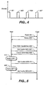
- Figure 4 is a schematic representation of the access pattern of an MP3 player as a function of time, where data is read at 401, 403, 405, and so on, with the dead time between a pair of reads indicated at 411.
- the controller can go into a power saving mode, engage in defect management or various heroics to save marginal data, or fix bad bits or sectors as these non-busy times have a fairly regular occurrence and duration.
- the profiling information of the host can give the card the ability to decide what are the best operations to do for the best performance of timings, quality, power consumption, and so on.
- the card controller will identify the host access profile to optimize its algorithms.
- the card will include a processor-based controller 131 that performs as the memory control.
- the memory can be based on other technologies, the exemplary embodiment will again be based on a flash memory.
- these cards are designed to be plugged into different devices, such as PDAs, digital cameras, cell phones, and so on, which access the card in different patterns.
- this differentiation in function causes the card a hit in performance and in the capability to optimize the memory management algorithms according to the host access pattern as the prior art lacks the algorithm optimization aspect of the present invention.
- the different hosts use different applications with the memory cards. These applications have different needs in terms of read/write performance, level of data integrity, etc. that is not taken into account in the prior art card controllers.
- the host profiling aspect of the present invention improves upon the prior art by having two modes of operation. In the first of these, the host profiling is by the card controller. The second is based on a quality of service negotiation between the card and the host. These operations will allow the card controller to tune its algorithms according to the data collected on the host.
- the various embodiments can be implemented in hardware or firmware.
- the card will learn about the host during its transactions and will collect information, such as write/read buffer transfer speed, the idle time between data buffers, block count in read/write, LBA rewrites, file access table (FAT) updates, idle time between sequential commands, and so on.
- the card will then use this information to optimize the memory control algorithms to the host. For example, on a host that reads slowly, such as an MP3 player, the card can handle correctable ECC errors by having the card controller read ahead enough sectors that will allow a safe correction in the flash memory without a degradation in performance.
- the card recognizes rewrites to the file access table, it can have FAT data caching in the card and update these sectors less frequently.
- a first example of host profiling by the card's controller is the profiling of the clock rate used on the card's system bus, for example the SD or MMC bus as described in the references above for these cards.
- the card's hardware can include a counter that will be incremented on every system bus clock. Such a counter 133 is shown in Figure 3 as part of the controller.
- the system's firmware knows the system's clock rate that the controller is running, a simple calculation allows the controller to determine the bus clock.
- the card's firmware can activate a timer to measure how long it takes the card to receive from or send to the host a specified number of sectors. This number could be any number (2, 4, 8, 16, and so on) and can be a settable parameter in firmware.
- the card can set its system clock (or clocks) to meet the host's transfer rate and minimize power consumption. As the higher the clock rate, the greater the power consumption of the card's controller, the controller's system clock(s) have a major impact over the card's power consumption. If the card system maintains a clock rate faster than needed to conform with the host's transfer rate, unnecessary power will be consumed, so by setting the system clock settings to meet the host transfer rate, the card optimizes its power consumption while maintaining performance.
- the card's firmware can hold a table to indicate the card's data transfer rate for a given clock setting. Once the card's profiling has determined the host's transfer rate, it can then use the minimum clock rates that allow the card to successfully supply the host's data transfer rate. This will allow the card's power consumption to be optimized. The firmware can continue to monitor the host's data transfer rate and update the controller's clock(s) setting(s) accordingly.
- the card can profile a host's block count for both read and write.
- the write and read commands do not have a defined block count and the termination of an operation is based on a stop transmission command.
- the card's firmware can determine whether an access by the host is to the file system area instead of the user data area.
- the firmware can read assigned area where the Master Boot Record (MBR) is stored, such as Logical Block Address (LBA) 0.
- MRR Master Boot Record
- LBA Logical Block Address
- the firmware can find the LBA range of the file system, such as (MBR + Partition Table + FAT1 + FAT2) in the MMC/SD card example, where FAT1 and FAT2 are the two copies of the file access table. Once the LBA range of the file system determined, any access to this address space by the host can be considered as access to file system area and not to user area.
- the firmware can find the block count used by the host to write data to the user space during write or read operations and the sequence of starting LBAs.
- the card's firmware can tune its algorithms and hardware to maximize performance and minimize power consumption. Examples of such tuning can include data caching, prioritizing tasks/interrupt service routines/direct memory accesses, determine garbage collection (data relocation) preferences (such as least recently used or most recently used blocks), and so on.
- garbage collection data relocation
- the priority order chosen can have a major impact on performance.
- the host requests the card report its capabilities and recommendation.
- the host will report to the card the configuration it prefers to work with and its profile for accessing the card.
- the card capabilities reported to the host can include: read/write speed, best write block count, best start logical block address (LBA) alignment, ECC capabilities correct/ignore/abort, performance versus current consumption, performance versus data retention, and other operating parameters. There are usually a number of trade offs between these in card design, and this process allows these parameters to be adapted to the particular application.
- the host profile reported to the card can include: write/read maximum speed; logical address offsets for data types (for example, the offset in number of blocks for user data with a start LBA and block count due to overhead, such as ( blocks devoted to list of transactions + start LBA + block count) or ( blocks devoted to FAT area - start LBA + block count ); the level of data integrity in acceptable in a read (for example, ECC errors can be corrected or can be ignored and the read continued; alternately, a bad block can be set to some pattern or the read can be aborted); and so on. All of the features described above for the host-profiling mode can also be implemented in the quality of service mode and vice versa. Additionally, it should be noted that these two modes are not exclusive of each other and be used in a complimentary manner.
- the card can use a different algorithm to write to these FAT blocks to minimize garbage collections.
- a host such as a PC
- the card can choose a high performance/high power consumption mode, such as using multiple plane or multichip programming (described in U.S. patent application Number 10/315,451, filed December 9, 2002 ); on the other hand, in a low power host, such as an MP3 player, the card can choose low performance and low power operation.
- the controller has the ability to adjust its own internal clock frequency such as by writing a value to a defined hardware register, the controller performance can be adjusted to meet that required by the application and can even be varied depending on external conditions. For example, in a high performance application, a maximum frequency may be desirable at the expense of increased power consumption, and an intelligent controller can measure suitable external variables such as temperature or power supply voltage and adjust the clock frequency accordingly. It is common to design an internal oscillator to be relatively constant with respect to temperature and voltage. However, CMOS circuits are normally capable of higher speed operation at lower temperatures and at higher voltages. The chip temperature can be measured, such as through the use of a temperature sensitive resistor or p-n junction, and the frequency set accordingly. Similarly the external voltage is easily measured using well know analog to digital converter circuitry and the internal oscillator frequency adjusted in response to this measurement. In this manner the application can override the normally pre-set clock frequency and obtain maximum performance under a variety of application and environmental condition.
- FIG. 5 is a diagrammatic illustration of an exemplary host-card quality of service negotiation process showing the exchanges that allow the card to choose the quality of service optimized for a given application.
- the host sends the card a reset signal 601.
- the reset signal in an MMC card embodiment is described further in U.S. patent application 09/186,064 , where the ability of the card to select the host's protocol based upon the reset signal is described.
- the card responds with a ready signal 603.
- the actually quality of service (QOS) negotiation begins, with the host sending its QOS capability data to the card 605 and requesting the cards QOS capabilities 607, where the order of these steps can be switched depending on the implementation.
- the card responds to the host with the card's QOS data 609. At this point, the host can put the card use in an application.
- QOS actually quality of service
- the host can set the card's configuration according to the host applications' needs. For instance, an MP3 application may require only require a low bit rate and low power, while an image-capture application may require the maintaining high bit rate, and so on.
- an MP3 application may require only require a low bit rate and low power
- an image-capture application may require the maintaining high bit rate, and so on.
- the host sets the card's QOS 611 optimized for the application: for example, it could be an application were the rate and consistency of data transfer is more important that minor amounts of error. In this case, the use of ECC could be used only in as much as it does not affect the transfer rate.
- the host can use the card in another application APP N 620 and resets the card's QOS 621 accordingly:
- application APP N could require data, such as in medical imaging, to be stored at with highest integrity with speed of far less importance.
- All of these embodiments have the card learning host profile in real time and tuning the memory management algorithms according the collected information for achieving the best performance. They also differ from the prior art in that the host and card negotiate over capabilities and the card sets the card operating algorithms according to the best configuration.
- FIG. 6 A particular implementation of the invention based on dynamic optimization through pattern recognition is described with respect to Figure 6 .
- the exemplary embodiment of Figure 6 allows the performance of storage devices to be optimized without having to analyze an overly large number of applications by allowing the storage device to dynamically self-optimize by monitoring for specific and typical patterns of host behavior. This improves upon prior art techniques, such as caching and other general performance enhancements.
- this implementation is again discussed in the context of a flash based non-volatile memory card, as are the various aspects and implementations discussed above, these concepts may be applied to other storage devices, such as in the optimization of dual storage devices such as a disk drive with flash memory device.
- the techniques of the embodiment of Figure 6 allow a storage device to memorize access sequences issued by the host under certain predefined conditions, such as host reset, power on boot sequence, various benchmarks and so on.
- the underlying concept is that when these predefined condition or "trigger patterns" occur, the sequence of host commands that follow them is usually identical. It should be noted that this matching is based on pattern matching, rather some sort of code matching mechanism.
- the storage device can use this information to optimize operation for those expected commands. Optimization could be by performing look ahead read caching to pre-fetch data, or other system type preparation that would speed up command execution. For example, when a host issues a reset, the portion of the memory storing the file access tables are most likely read first, so the card could use this as a trigger.
- the device On deviation from expected command or control sequence, the device would memorize the new command sequence and save to permanent storage thus becoming self-adaptive. Similarly, if an already stored pattern is changed, the stored pattern is updated to reflect the variation or extension of the pattern. Several different patterns and command sequences may be stored.
- the process starts at 501 with the card connected to the host and at step 503 any initial or additional set of patterns and command sequences are loaded onto the card.
- a number of such patterns may be predefined in firmware, although these need not be complete patterns.
- the card itself can complete the process, thereby saving on initial engineering time. Typical patterns could include command sequences and single commands, reset, power cycle, and so on.
- the card will monitor the host-card interactions at step 505, seeing whether a match occurs with any of the stored patterns. This continues (the "No" loop from 507) until a match is detected at step 507, when it moves to step 509.
- the card can pre-execute the command sequence corresponding to pattern, as shown at step 509.
- the actual action taken may depend upon implementation and may be actions in preparation for the command or the actual execution of the command, such as a read operation to fill a cache or doing a seek to an expected location in the memory, preloading control information or tables, or performing logical to physical address translations. Controller 131 ( Figure 3 ) would handle the processing involved in these processes.
- the card will check the command against the stored command sequence list (step 511) and determine (step 513) if the command previously selected as matching in step 507 based upon its initial portion continues to correspond. If so, the command will be executed in step 517 using the previous optimization.
- step 515 the card determines if the end of the list has been reached and, if so, to return to monitoring the host at step 505. Note that for the case where the entries of the list have an order, such a series of logical block addresses to read, it can be determined that the command does not match a list entry without having to exhaust the list.
- step 515 finds that it is not the end of the list, the flow continues to step 519 for the dynamic updating portion of the process.
- step 519 the command is executed and the new sequence is stored in the memory, such as RAM 121 of Figure 3 , so that it can be saved to the command list when it is updated. It the list has not been previously exhausted, this process continues (the "No" loop from 521) until the end of the list is reached, as determined in step 521, at which point the list of saved commands is updated (step 523). For example, if the signature access of a benchmark changes so that its later portion is different than the previous value (say, switching a logical address to be read), this would be covered in the updating by revising this portion of the benchmark sequence. Once the updating is complete, the process returns to step 505 and monitors the host.
- a non-volatile memory is organized into a series of "zones", such as is described in U.S. patent application 10/315,451 filed December 9, 2002 .
- various data used as part of the boot process such as the file access table (FAT) is stored in a specific area, which can be taken as part of zone 0.
- FAT file access table
- Figure 7 can used be to illustrate this situation, where the top row illustrates the prior art process and the bottom row shows how this would be changed from the prior art.
- the top row of Figure 7 is similar to Figure 4 , but with additional detail.
- the controller receives a command or control sequence (451a, 453a, 455a, ...) and responds. Each response consists of a corresponding preparation portion (451b, 453b, 455b, ...) and operation portion (451c, 453c, 455c, ).
- the controller will wait for the command, such as 453a, before executing the corresponding preparation and operation, 453b and 453c.
- the subsequent preparation portions can be moved into the dead time ahead of the next command, as is shown in the bottom row of Figure 7 .
- the controller finds a match in the control signal 451a.
- the corresponding preparation and operation phases (451b, 451c) are executed afterwards; however, the preparation for the expected next command (453b), such as caching data or a seek, is also executed prior to the arrival of the corresponding signal 453a at the controller.
- the preparation phase is already completed and the controller proceeds directly to the operation 453c. (If 453a is not a match, the correction preparation phase would be performed as in the top row and nothing is lost and the stored sequence can be subsequently updated)
- the process continues similarly for the set 455a-c and so on for the rest of the control sequence. This results in the hiding the preparation time for each part of the sequence after the first where the pattern is matched. For example, through 455c in Figure 7 , the process has the resultant time saving of ⁇ t due to pre-executing the "b" portions of the commands.
- zone 0 is most likely to be accessed (to retrieve the FAT), followed by, say, zone 5 and then zone 1.
- the controller may as well login to zone 5 and be ready. If 451, 453, and 455 respectively correspond to the respective combined access times for zones 0, 5, and 1 in the exemplary process, by moving the login and pre-fetch time (453b in Figure 7 ) into the preceding dead time, the access time needed for zone 5 is correspondingly reduced, with similar savings available in the other access times. If the sequence of commands does not go to the expected zone 5, as this login was performed during an idle time, nothing is lost. Additionally, if the boot process changes, from, say, the exemplary 0-5-1 to 0-5-3, or is extended, to, say, 0-5-1-4, this will be dynamically updated.
- the dynamic optimization through pattern recognition described with respect to Figure 6 can either be left functioning once the memory system is shipped and in the field, allowing for continued optimization during use by the consumer, or be used prior to shipping and then fixed.
- the standard method of optimizing a card at the factory for a specific application or set of applications required a study of the hosts' access patterns. Once these had been analyzed, the cards' firmware was tuned accordingly.
- the present invention allows the storage device itself to learn. The storage device can start with only a few partial patterns, or no patterns, stored on the device. The card can then be run through a number of applications, such as benchmark utilities or boot sequences, and the corresponding patterns learned and stored. At this point, the learned processes could be fixed if desired and the product shipped.
- the controller can adapt to the card to other external conditions.
- flash memories such as those found in the exemplary embodiments above
- conditions external to the memory card that may affect card operation are when the battery is low on host device.
- chip temperature can be measured, such as through the use of a temperature sensitive resistor or p-n junction, and the frequency set accordingly.
- the external voltage is easily measured using well know analog to digital converter circuitry and the internal oscillator frequency adjusted in response to this measurement. In this manner the application can override the normally pre-set clock frequency and obtain adjust performance to a variety of external conditions.
- the controller could operate the memory in a more reliable manner. This could be done in various ways similar to those already described, such as lowering performance, increased use of ECC or margining, and so on.
- the sensing of such conditions can be accomplished using reference cells in the memory or other techniques, such as described in U.S. patent number 5,694,356 .
- the particular conditions to which the controller responds, and how it does so, would correspond to the memory technologies (e.g. thin film, MRAM, FRAM, NMOS, etc.) employed.
Claims (13)
- Procédé d'exploitation d'une carte mémoire non volatile (35, 100), consistant à :recevoir une séquence (451a - 451c, 453a - 453c, 455a - 455c) d'un ou plusieurs signaux de commande à partir d'un hôte (31, 160) ;le procédé étant caractérisé en ce qu'il consiste à :déterminer (507) si une partie initiale de la séquence reçue (451a - 451c, 453a - 453c, 455a - 455c) correspond à l'un d'un ensemble d'un ou plusieurs motifs stockés sur la carte (35, 100), où ladite partie initiale est inférieure à la séquence reçue intégrale (451a - 451c, 453a - 453c, 455a - 455c) ;lorsque ladite partie initiale de la séquence reçue (451a - 451c, 453a - 453c, 455a - 455c) correspond à l'un desdits motifs, optimiser (509) la carte (35, 100) en vue de mettre en oeuvre une séquence correspondante parmi un ensemble de séquences de commande stockées sur la carte (35, 100), avant de recevoir la séquence reçue intégrale (451a - 451c, 453a - 453c, 455a - 455c), dans lequel chaque séquence de l'ensemble de séquences de commande stockées présente une partie initiale correspondant à l'un de l'ensemble de motifs stockés ; etdéterminer (513) si la partie de la séquence reçue (451a - 451c, 453a - 453c, 455a - 455c) subséquemment à ladite partie initiale correspond à ladite séquence stockée correspondante.
- Procédé selon la revendication 1, consistant en outre à :lorsque ladite séquence reçue subséquemment à ladite partie initiale ne correspond pas à ladite séquence stockée correspondante, mettre à jour (523) ledit ensemble de séquences de commande stockées sur la carte (35, 100) en vue d'inclure la séquence reçue (451a - 451c, 453a - 453c, 455a - 455c).
- Procédé selon la revendication 2, dans lequel ladite mise à jour (523) consiste à modifier une séquence de commande précédemment stockée sur la carte (35, 100).
- Procédé selon la revendication 1 ou 2, consistant en outre à :verrouiller ledit ensemble de séquences de commande stockées sur la carte (35, 100) de sorte qu'elles ne peuvent plus être mises à jour.
- Procédé selon la revendication 1, consistant en outre à :lorsque ladite séquence reçue (451a - 451c, 453a - 453c, 455a - 455c) subséquemment à ladite partie initiale correspond à ladite séquence stockée correspondante, exécuter (517) ladite séquence de commande stockée correspondante.
- Procédé selon la revendication 1, dans lequel ladite optimisation (509) de la carte (35, 100) inclut la pré-exécution d'une partie de ladite séquence de commande stockée correspondante.
- Procédé selon la revendication 1, dans lequel ladite optimisation (509) de la carte (35, 100) inclut la mise en cache de données.
- Procédé selon la revendication 1, dans lequel ladite optimisation (509) de la carte (35, 100) inclut la mise en oeuvre d'une recherche.
- Procédé selon la revendication 1, dans lequel ladite optimisation (509) de la carte (35, 100) inclut la mise en oeuvre d'une traduction logique à physique.
- Procédé selon la revendication 1, dans lequel ladite optimisation (509) de la carte (35, 100) inclut la préparation d'activités pour une séquence de commande.
- Procédé selon la revendication 1, dans lequel ledit ensemble de séquences de commande stockées comprend une séquence d'amorçage.
- Procédé selon la revendication 1, dans lequel ledit ensemble de séquences de commande stockées comprend une ou plusieurs séquences de base.
- Procédé selon la revendication 1, dans lequel ledit ensemble de séquences de commande stockées comprend une réinitialisation d'hôte (31, 160).
Applications Claiming Priority (2)
| Application Number | Priority Date | Filing Date | Title |
|---|---|---|---|
| US10/901,849 US7427027B2 (en) | 2004-07-28 | 2004-07-28 | Optimized non-volatile storage systems |
| EP05773779A EP1782223B1 (fr) | 2004-07-28 | 2005-07-20 | Systemes de stockages non-volatiles optimises |
Related Parent Applications (1)
| Application Number | Title | Priority Date | Filing Date |
|---|---|---|---|
| EP05773779.3 Division | 2005-07-20 |
Publications (2)
| Publication Number | Publication Date |
|---|---|
| EP2386961A1 EP2386961A1 (fr) | 2011-11-16 |
| EP2386961B1 true EP2386961B1 (fr) | 2013-09-11 |
Family
ID=35432403
Family Applications (2)
| Application Number | Title | Priority Date | Filing Date |
|---|---|---|---|
| EP05773779A Active EP1782223B1 (fr) | 2004-07-28 | 2005-07-20 | Systemes de stockages non-volatiles optimises |
| EP11176847.9A Not-in-force EP2386961B1 (fr) | 2004-07-28 | 2005-07-20 | Systèmes optimisés de stockage non volatile |
Family Applications Before (1)
| Application Number | Title | Priority Date | Filing Date |
|---|---|---|---|
| EP05773779A Active EP1782223B1 (fr) | 2004-07-28 | 2005-07-20 | Systemes de stockages non-volatiles optimises |
Country Status (7)
| Country | Link |
|---|---|
| US (3) | US7427027B2 (fr) |
| EP (2) | EP1782223B1 (fr) |
| JP (1) | JP2008518283A (fr) |
| KR (2) | KR101153232B1 (fr) |
| AT (1) | ATE547759T1 (fr) |
| TW (1) | TWI372977B (fr) |
| WO (1) | WO2006014791A2 (fr) |
Families Citing this family (76)
| Publication number | Priority date | Publication date | Assignee | Title |
|---|---|---|---|---|
| US8171192B2 (en) * | 2005-09-20 | 2012-05-01 | Qualcomm Incorporated | Hardware-assisted device configuration detection |
| KR101346734B1 (ko) * | 2006-05-12 | 2014-01-03 | 삼성전자주식회사 | 디지털 저작권 관리를 위한 다중 인증서 철회 목록 지원방법 및 장치 |
| KR100845525B1 (ko) * | 2006-08-07 | 2008-07-10 | 삼성전자주식회사 | 메모리 카드 시스템, 그것의 데이터 전송 방법, 그리고반도체 메모리 장치 |
| KR100801014B1 (ko) * | 2006-08-21 | 2008-02-04 | 삼성전자주식회사 | Dos 부트 프로그램을 내장한 디스크를 구비하는 하드 디스크 드라이브와 그를 포함하는 컴퓨터 시스템, 상기 하드 디스크 드라이브의 펌웨어 다운로드 방법 및 그를 포함하는 기록 매체 |
| TW200813856A (en) * | 2006-09-15 | 2008-03-16 | Alcor Micro Corp | USB peripheral device with dynamic change class and application thereof |
| FR2908195B1 (fr) * | 2006-11-06 | 2009-02-06 | Oberthur Card Syst Sa | Procede de passation d'instructions entre une station hote et un dispositif electronique portable, et dispositif de mise en oeuvre |
| KR100823166B1 (ko) * | 2006-12-04 | 2008-04-18 | 삼성전자주식회사 | 통신 속도가 향상된 메모리 카드 및 메모리 카드를포함하는 메모리 카드 시스템 |
| JP4970078B2 (ja) * | 2007-02-21 | 2012-07-04 | 株式会社東芝 | 不揮発性メモリシステム |
| WO2008108084A1 (fr) * | 2007-03-02 | 2008-09-12 | Panasonic Corporation | Appareil de reproduction, intégration à grande échelle (lsi) de système et procédé d'initialisation |
| US7853759B2 (en) * | 2007-04-23 | 2010-12-14 | Microsoft Corporation | Hints model for optimization of storage devices connected to host and write optimization schema for storage devices |
| US7788415B2 (en) * | 2007-05-28 | 2010-08-31 | Sandisk Il Ltd. | Management of internal operations by a storage device |
| US20110066768A1 (en) * | 2007-07-23 | 2011-03-17 | Rod Brittner | Quality of service and streaming attributes for a data storage device |
| US9098506B2 (en) | 2008-01-02 | 2015-08-04 | Sandisk Il, Ltd. | Data indexing by local storage device |
| US8583878B2 (en) | 2008-01-02 | 2013-11-12 | Sandisk Il Ltd. | Storage device having direct user access |
| KR20100106609A (ko) * | 2008-01-02 | 2010-10-01 | 샌디스크 아이엘 엘티디 | 직접적인 사용자 액세스를 갖는 저장 장치 |
| US8452927B2 (en) | 2008-01-02 | 2013-05-28 | Sandisk Technologies Inc. | Distributed storage service systems and architecture |
| US8307180B2 (en) | 2008-02-28 | 2012-11-06 | Nokia Corporation | Extended utilization area for a memory device |
| CN102090055A (zh) * | 2008-07-14 | 2011-06-08 | 松下电器产业株式会社 | 影像数据处理装置和影像数据处理方法 |
| US8209439B2 (en) * | 2008-08-25 | 2012-06-26 | Sandisk Il Ltd. | Managing multiple concurrent operations with various priority levels in a local storage device |
| TWI386800B (zh) * | 2008-10-03 | 2013-02-21 | Silicon Motion Inc | 快閃記憶體之更新資料的管理方法以及相關之記憶卡 |
| US8069324B2 (en) * | 2008-12-19 | 2011-11-29 | Seagate Technology Llc | Storage device with manual learning |
| US8924661B1 (en) * | 2009-01-18 | 2014-12-30 | Apple Inc. | Memory system including a controller and processors associated with memory devices |
| US20110304531A1 (en) * | 2010-06-10 | 2011-12-15 | Peter Brooks | Method and system for interfacing and interaction with location-aware devices |
| US10031850B2 (en) | 2011-06-07 | 2018-07-24 | Sandisk Technologies Llc | System and method to buffer data |
| US9098399B2 (en) | 2011-08-31 | 2015-08-04 | SMART Storage Systems, Inc. | Electronic system with storage management mechanism and method of operation thereof |
| US9063844B2 (en) | 2011-09-02 | 2015-06-23 | SMART Storage Systems, Inc. | Non-volatile memory management system with time measure mechanism and method of operation thereof |
| JP2013077278A (ja) | 2011-09-16 | 2013-04-25 | Toshiba Corp | メモリ・デバイス |
| JP5694101B2 (ja) | 2011-09-20 | 2015-04-01 | 株式会社東芝 | メモリ・デバイス、ホスト・デバイス |
| JP5547154B2 (ja) | 2011-09-21 | 2014-07-09 | 株式会社東芝 | メモリ・デバイス |
| US20130151755A1 (en) | 2011-12-12 | 2013-06-13 | Reuven Elhamias | Non-Volatile Storage Systems with Go To Sleep Adaption |
| US9239781B2 (en) | 2012-02-07 | 2016-01-19 | SMART Storage Systems, Inc. | Storage control system with erase block mechanism and method of operation thereof |
| US20130282962A1 (en) * | 2012-04-20 | 2013-10-24 | SMART Storage Systems, Inc. | Storage control system with flash configuration and method of operation thereof |
| US9671962B2 (en) | 2012-11-30 | 2017-06-06 | Sandisk Technologies Llc | Storage control system with data management mechanism of parity and method of operation thereof |
| US9123445B2 (en) | 2013-01-22 | 2015-09-01 | SMART Storage Systems, Inc. | Storage control system with data management mechanism and method of operation thereof |
| US9214965B2 (en) | 2013-02-20 | 2015-12-15 | Sandisk Enterprise Ip Llc | Method and system for improving data integrity in non-volatile storage |
| US9329928B2 (en) | 2013-02-20 | 2016-05-03 | Sandisk Enterprise IP LLC. | Bandwidth optimization in a non-volatile memory system |
| US9183137B2 (en) | 2013-02-27 | 2015-11-10 | SMART Storage Systems, Inc. | Storage control system with data management mechanism and method of operation thereof |
| US10049037B2 (en) | 2013-04-05 | 2018-08-14 | Sandisk Enterprise Ip Llc | Data management in a storage system |
| US9170941B2 (en) | 2013-04-05 | 2015-10-27 | Sandisk Enterprises IP LLC | Data hardening in a storage system |
| US9543025B2 (en) | 2013-04-11 | 2017-01-10 | Sandisk Technologies Llc | Storage control system with power-off time estimation mechanism and method of operation thereof |
| US10546648B2 (en) | 2013-04-12 | 2020-01-28 | Sandisk Technologies Llc | Storage control system with data management mechanism and method of operation thereof |
| KR102098246B1 (ko) | 2013-04-29 | 2020-04-07 | 삼성전자 주식회사 | 호스트, 저장 장치, 및 이를 포함하는 시스템의 동작 방법 |
| US9367353B1 (en) | 2013-06-25 | 2016-06-14 | Sandisk Technologies Inc. | Storage control system with power throttling mechanism and method of operation thereof |
| US9244519B1 (en) | 2013-06-25 | 2016-01-26 | Smart Storage Systems. Inc. | Storage system with data transfer rate adjustment for power throttling |
| US9146850B2 (en) | 2013-08-01 | 2015-09-29 | SMART Storage Systems, Inc. | Data storage system with dynamic read threshold mechanism and method of operation thereof |
| US9361222B2 (en) | 2013-08-07 | 2016-06-07 | SMART Storage Systems, Inc. | Electronic system with storage drive life estimation mechanism and method of operation thereof |
| US9431113B2 (en) | 2013-08-07 | 2016-08-30 | Sandisk Technologies Llc | Data storage system with dynamic erase block grouping mechanism and method of operation thereof |
| US9448946B2 (en) | 2013-08-07 | 2016-09-20 | Sandisk Technologies Llc | Data storage system with stale data mechanism and method of operation thereof |
| US9747157B2 (en) | 2013-11-08 | 2017-08-29 | Sandisk Technologies Llc | Method and system for improving error correction in data storage |
| US9152555B2 (en) | 2013-11-15 | 2015-10-06 | Sandisk Enterprise IP LLC. | Data management with modular erase in a data storage system |
| US9411721B2 (en) | 2013-11-15 | 2016-08-09 | Sandisk Technologies Llc | Detecting access sequences for data compression on non-volatile memory devices |
| KR20150068747A (ko) | 2013-12-12 | 2015-06-22 | 삼성전자주식회사 | 비휘발성 메모리 시스템, 이를 포함하는 모바일 장치 및 비휘발성 메모리 시스템의 동작방법 |
| WO2015089488A1 (fr) | 2013-12-12 | 2015-06-18 | Memory Technologies Llc | Modules de mémorisation optimisée à canaux |
| US9280419B2 (en) | 2013-12-16 | 2016-03-08 | International Business Machines Corporation | Dynamic adjustment of data protection schemes in flash storage systems based on temperature, power off duration and flash age |
| US9977628B2 (en) * | 2014-04-16 | 2018-05-22 | Sandisk Technologies Llc | Storage module and method for configuring the storage module with memory operation parameters |
| USD736212S1 (en) * | 2014-07-01 | 2015-08-11 | Samsung Electronics Co., Ltd. | Memory card |
| USD736213S1 (en) * | 2014-07-01 | 2015-08-11 | Samsung Electronics Co., Ltd. | Memory card |
| KR102285789B1 (ko) | 2014-07-01 | 2021-08-04 | 삼성전자 주식회사 | 외장 저장 장치, 및 이의 기준 주파수를 설정하는 방법 |
| USD739856S1 (en) * | 2014-07-30 | 2015-09-29 | Samsung Electronics Co., Ltd. | Memory card |
| USD736216S1 (en) * | 2014-07-30 | 2015-08-11 | Samsung Electronics Co., Ltd. | Memory card |
| TWI553476B (zh) * | 2015-03-05 | 2016-10-11 | 光寶電子(廣州)有限公司 | 區域描述元管理方法及其電子裝置 |
| US10592122B2 (en) | 2015-03-31 | 2020-03-17 | Sandisk Technologies Llc | Inherent adaptive trimming |
| US9904477B2 (en) | 2015-05-13 | 2018-02-27 | Sandisk Technologies Llc | System and method for storing large files in a storage device |
| USD783622S1 (en) * | 2015-08-25 | 2017-04-11 | Samsung Electronics Co., Ltd. | Memory card |
| USD783621S1 (en) * | 2015-08-25 | 2017-04-11 | Samsung Electronics Co., Ltd. | Memory card |
| KR102547795B1 (ko) | 2016-05-04 | 2023-06-27 | 에스케이하이닉스 주식회사 | 데이터 처리 시스템 및 데이터 처리 시스템의 동작 방법 |
| US10037213B2 (en) | 2016-09-19 | 2018-07-31 | Nxp Usa, Inc. | System and method for adjusting boot interface frequency |
| US10978790B2 (en) * | 2017-09-12 | 2021-04-13 | Mark P Kramer | Electromagnetic radiation attenuating device for laptop computers |
| CN109002257B (zh) * | 2018-06-25 | 2021-04-23 | 重庆邮电大学 | 一种基于可变便笺存储器的数据分布优化方法 |
| US10725705B1 (en) | 2019-01-16 | 2020-07-28 | Western Digital Technologies, Inc. | System and method for storage system property deviation |
| US10908844B2 (en) | 2019-06-18 | 2021-02-02 | Western Digital Technologies, Inc. | Storage system and method for memory backlog hinting for variable capacity |
| US11137932B2 (en) | 2019-12-02 | 2021-10-05 | Western Digital Technologies, Inc. | Pad indication for device capability |
| KR20220067992A (ko) | 2020-11-18 | 2022-05-25 | 삼성전자주식회사 | 선택적 및 병렬적 에러 정정을 수행하는 메모리 컨트롤러, 이를 포함하는 시스템 및 메모리 장치의 동작 방법 |
| US20230315295A1 (en) * | 2022-03-30 | 2023-10-05 | Micron Technology, Inc. | Dynamic memory device management and stream prioritization based on quality of service metrics |
| WO2023211232A1 (fr) * | 2022-04-28 | 2023-11-02 | 김정기 | Lecteur de carte mémoire équipé d'une fonction de suppression et d'optimisation de données |
| KR102632266B1 (ko) * | 2022-04-28 | 2024-02-01 | 김정기 | 자체 데이터 삭제 기능을 내장한 메모리 카드 리더기 |
Family Cites Families (31)
| Publication number | Priority date | Publication date | Assignee | Title |
|---|---|---|---|---|
| DE69033438T2 (de) | 1989-04-13 | 2000-07-06 | Sandisk Corp | Austausch von fehlerhaften Speicherzellen einer EEprommatritze |
| US5172338B1 (en) | 1989-04-13 | 1997-07-08 | Sandisk Corp | Multi-state eeprom read and write circuits and techniques |
| JP2854680B2 (ja) * | 1990-06-15 | 1999-02-03 | 株式会社東芝 | Icメモリカード |
| US5857059A (en) * | 1991-10-31 | 1999-01-05 | Canon Kabushiki Kaisha | Information recording apparatus |
| US5659690A (en) | 1992-10-15 | 1997-08-19 | Adaptec, Inc. | Programmably configurable host adapter integrated circuit including a RISC processor |
| US5694356A (en) | 1994-11-02 | 1997-12-02 | Invoice Technology, Inc. | High resolution analog storage EPROM and flash EPROM |
| JP3604466B2 (ja) * | 1995-09-13 | 2004-12-22 | 株式会社ルネサステクノロジ | フラッシュディスクカード |
| US5784599A (en) | 1995-12-15 | 1998-07-21 | Compaq Computer Corporation | Method and apparatus for establishing host bus clock frequency and processor core clock ratios in a multi-processor computer system |
| JP3493096B2 (ja) * | 1996-06-07 | 2004-02-03 | 株式会社東芝 | 半導体集積回路、icカード、及びicカードシステム |
| JPH10170564A (ja) * | 1996-12-13 | 1998-06-26 | Nec Eng Ltd | クロック周波数測定回路及びその方法 |
| US6055593A (en) | 1996-12-31 | 2000-04-25 | Intel Corporation | Dual information structures for different electronic data storage card environments |
| JP3233079B2 (ja) | 1997-09-30 | 2001-11-26 | ソニー株式会社 | データ処理システム及びデータ処理方法 |
| US6076137A (en) | 1997-12-11 | 2000-06-13 | Lexar Media, Inc. | Method and apparatus for storing location identification information within non-volatile memory devices |
| US6182162B1 (en) | 1998-03-02 | 2001-01-30 | Lexar Media, Inc. | Externally coupled compact flash memory card that configures itself one of a plurality of appropriate operating protocol modes of a host computer |
| JP3714969B2 (ja) | 1998-03-02 | 2005-11-09 | レクサー・メディア・インコーポレイテッド | 改良されたオペレーティングモード検出機能を備えたフラッシュメモリーカード及びユーザフレンドリなインターフェーシングシステム |
| US6040622A (en) | 1998-06-11 | 2000-03-21 | Sandisk Corporation | Semiconductor package using terminals formed on a conductive layer of a circuit board |
| JP2000181784A (ja) * | 1998-12-18 | 2000-06-30 | Hitachi Ltd | 書き換え可能な不揮発性記憶装置 |
| JP2001125829A (ja) * | 1999-10-28 | 2001-05-11 | Internatl Business Mach Corp <Ibm> | コントローラ装置、ディスクコントローラ、補助記憶装置、コンピュータ装置、および補助記憶装置の制御方法 |
| US6578125B2 (en) | 2000-02-14 | 2003-06-10 | Sanyo Electric Co., Ltd. | Memory access circuit and memory access control circuit |
| JP2001297316A (ja) * | 2000-04-14 | 2001-10-26 | Mitsubishi Electric Corp | メモリカード及びその制御方法 |
| US6820148B1 (en) * | 2000-08-17 | 2004-11-16 | Sandisk Corporation | Multiple removable non-volatile memory cards serially communicating with a host |
| JP3923715B2 (ja) | 2000-09-29 | 2007-06-06 | 株式会社東芝 | メモリカード |
| US6993605B2 (en) * | 2001-02-28 | 2006-01-31 | Sharp Laboratories Of America, Inc. | Adaptive run-time data transfer optimization |
| US7114001B2 (en) * | 2001-05-11 | 2006-09-26 | International Business Machines Corporation | Predictive networking |
| JP4841070B2 (ja) | 2001-07-24 | 2011-12-21 | パナソニック株式会社 | 記憶装置 |
| JP4841069B2 (ja) | 2001-07-24 | 2011-12-21 | パナソニック株式会社 | 記憶装置 |
| KR100441601B1 (ko) * | 2001-10-19 | 2004-07-23 | 삼성전자주식회사 | 메모리 카드, 디지털 기기 및 메모리 카드와 디지털 기기사이의 데이터 인터페이스 방법 |
| US7107420B2 (en) * | 2003-08-29 | 2006-09-12 | International Business Machines Corporation | Apparatus and method to adjust data transfer rate |
| US7478260B2 (en) * | 2003-10-20 | 2009-01-13 | Hewlett-Packard Development Company, L.P. | System and method for setting a clock rate in a memory card |
| TW200604810A (en) * | 2004-02-20 | 2006-02-01 | Renesas Tech Corp | Nonvolatile memory and data processing system |
| US7596643B2 (en) * | 2007-02-07 | 2009-09-29 | Siliconsystems, Inc. | Storage subsystem with configurable buffer |
-
2004
- 2004-07-28 US US10/901,849 patent/US7427027B2/en active Active
-
2005
- 2005-07-20 KR KR1020077002213A patent/KR101153232B1/ko active IP Right Grant
- 2005-07-20 AT AT05773779T patent/ATE547759T1/de active
- 2005-07-20 EP EP05773779A patent/EP1782223B1/fr active Active
- 2005-07-20 WO PCT/US2005/025983 patent/WO2006014791A2/fr active Application Filing
- 2005-07-20 JP JP2007523657A patent/JP2008518283A/ja active Pending
- 2005-07-20 KR KR1020117027483A patent/KR101182601B1/ko active IP Right Grant
- 2005-07-20 EP EP11176847.9A patent/EP2386961B1/fr not_active Not-in-force
- 2005-07-28 TW TW094125592A patent/TWI372977B/zh active
-
2008
- 2008-07-02 US US12/166,533 patent/US7926720B2/en active Active
-
2011
- 2011-03-14 US US13/047,631 patent/US8292177B2/en active Active
Also Published As
| Publication number | Publication date |
|---|---|
| EP1782223B1 (fr) | 2012-02-29 |
| US20110167186A1 (en) | 2011-07-07 |
| US20080270639A1 (en) | 2008-10-30 |
| KR101153232B1 (ko) | 2012-06-13 |
| JP2008518283A (ja) | 2008-05-29 |
| EP2386961A1 (fr) | 2011-11-16 |
| US20060022054A1 (en) | 2006-02-02 |
| KR101182601B1 (ko) | 2012-09-18 |
| WO2006014791A2 (fr) | 2006-02-09 |
| US7427027B2 (en) | 2008-09-23 |
| KR20110134520A (ko) | 2011-12-14 |
| WO2006014791A3 (fr) | 2008-04-03 |
| TW200627171A (en) | 2006-08-01 |
| US7926720B2 (en) | 2011-04-19 |
| KR20070051259A (ko) | 2007-05-17 |
| ATE547759T1 (de) | 2012-03-15 |
| EP1782223A2 (fr) | 2007-05-09 |
| US8292177B2 (en) | 2012-10-23 |
| TWI372977B (en) | 2012-09-21 |
Similar Documents
| Publication | Publication Date | Title |
|---|---|---|
| EP2386961B1 (fr) | Systèmes optimisés de stockage non volatile | |
| US11157182B2 (en) | Storage systems with go to sleep adaption | |
| US11829601B2 (en) | Extended utilization area for a memory device | |
| KR101911591B1 (ko) | 부트-업 시퀀스 예측 및 개선을 위한 시스템 및 방법 | |
| US20130060994A1 (en) | Non-volatile memory management system with time measure mechanism and method of operation thereof | |
| CN113342705A (zh) | 在存储器系统中执行垃圾收集的设备和方法 | |
| KR20210039171A (ko) | 메모리 시스템을 포함하는 데이터 처리 시스템에서 동작 정보를 송수신하는 방법 및 장치 | |
| CN113448503B (zh) | 调整顺序命令的操作时间差的存储器系统及其操作方法 | |
| US20210064242A1 (en) | Memory system for predicting whether internal operation is performable and data processing system including the same | |
| CN111831577A (zh) | 用于确定存储器系统中的存储块的特性的设备和方法 | |
| CN114327265A (zh) | 读取干扰检查方法、存储器存储装置及控制电路单元 | |
| CN112540932A (zh) | 存储控制器以及写入辅助方法 |
Legal Events
| Date | Code | Title | Description |
|---|---|---|---|
| 17P | Request for examination filed |
Effective date: 20110808 |
|
| AC | Divisional application: reference to earlier application |
Ref document number: 1782223 Country of ref document: EP Kind code of ref document: P |
|
| AK | Designated contracting states |
Kind code of ref document: A1 Designated state(s): AT BE BG CH CY CZ DE DK EE ES FI FR GB GR HU IE IS IT LI LT LU LV MC NL PL PT RO SE SI SK TR |
|
| PUAI | Public reference made under article 153(3) epc to a published international application that has entered the european phase |
Free format text: ORIGINAL CODE: 0009012 |
|
| RIC1 | Information provided on ipc code assigned before grant |
Ipc: G06F 13/38 20060101AFI20120918BHEP |
|
| GRAP | Despatch of communication of intention to grant a patent |
Free format text: ORIGINAL CODE: EPIDOSNIGR1 |
|
| GRAS | Grant fee paid |
Free format text: ORIGINAL CODE: EPIDOSNIGR3 |
|
| RAP1 | Party data changed (applicant data changed or rights of an application transferred) |
Owner name: SANDISK TECHNOLOGIES INC. |
|
| GRAA | (expected) grant |
Free format text: ORIGINAL CODE: 0009210 |
|
| AC | Divisional application: reference to earlier application |
Ref document number: 1782223 Country of ref document: EP Kind code of ref document: P |
|
| AK | Designated contracting states |
Kind code of ref document: B1 Designated state(s): AT BE BG CH CY CZ DE DK EE ES FI FR GB GR HU IE IS IT LI LT LU LV MC NL PL PT RO SE SI SK TR |
|
| REG | Reference to a national code |
Ref country code: GB Ref legal event code: FG4D |
|
| REG | Reference to a national code |
Ref country code: CH Ref legal event code: EP |
|
| REG | Reference to a national code |
Ref country code: AT Ref legal event code: REF Ref document number: 631975 Country of ref document: AT Kind code of ref document: T Effective date: 20130915 |
|
| REG | Reference to a national code |
Ref country code: IE Ref legal event code: FG4D |
|
| REG | Reference to a national code |
Ref country code: DE Ref legal event code: R096 Ref document number: 602005041237 Country of ref document: DE Effective date: 20131107 |
|
| REG | Reference to a national code |
Ref country code: NL Ref legal event code: T3 |
|
| PG25 | Lapsed in a contracting state [announced via postgrant information from national office to epo] |
Ref country code: CY Free format text: LAPSE BECAUSE OF FAILURE TO SUBMIT A TRANSLATION OF THE DESCRIPTION OR TO PAY THE FEE WITHIN THE PRESCRIBED TIME-LIMIT Effective date: 20130731 Ref country code: SE Free format text: LAPSE BECAUSE OF FAILURE TO SUBMIT A TRANSLATION OF THE DESCRIPTION OR TO PAY THE FEE WITHIN THE PRESCRIBED TIME-LIMIT Effective date: 20130911 Ref country code: LT Free format text: LAPSE BECAUSE OF FAILURE TO SUBMIT A TRANSLATION OF THE DESCRIPTION OR TO PAY THE FEE WITHIN THE PRESCRIBED TIME-LIMIT Effective date: 20130911 |
|
| REG | Reference to a national code |
Ref country code: AT Ref legal event code: MK05 Ref document number: 631975 Country of ref document: AT Kind code of ref document: T Effective date: 20130911 |
|
| REG | Reference to a national code |
Ref country code: LT Ref legal event code: MG4D |
|
| PG25 | Lapsed in a contracting state [announced via postgrant information from national office to epo] |
Ref country code: FI Free format text: LAPSE BECAUSE OF FAILURE TO SUBMIT A TRANSLATION OF THE DESCRIPTION OR TO PAY THE FEE WITHIN THE PRESCRIBED TIME-LIMIT Effective date: 20130911 Ref country code: SI Free format text: LAPSE BECAUSE OF FAILURE TO SUBMIT A TRANSLATION OF THE DESCRIPTION OR TO PAY THE FEE WITHIN THE PRESCRIBED TIME-LIMIT Effective date: 20130911 Ref country code: GR Free format text: LAPSE BECAUSE OF FAILURE TO SUBMIT A TRANSLATION OF THE DESCRIPTION OR TO PAY THE FEE WITHIN THE PRESCRIBED TIME-LIMIT Effective date: 20131212 Ref country code: LV Free format text: LAPSE BECAUSE OF FAILURE TO SUBMIT A TRANSLATION OF THE DESCRIPTION OR TO PAY THE FEE WITHIN THE PRESCRIBED TIME-LIMIT Effective date: 20130911 |
|
| PG25 | Lapsed in a contracting state [announced via postgrant information from national office to epo] |
Ref country code: CY Free format text: LAPSE BECAUSE OF FAILURE TO SUBMIT A TRANSLATION OF THE DESCRIPTION OR TO PAY THE FEE WITHIN THE PRESCRIBED TIME-LIMIT Effective date: 20130911 Ref country code: BE Free format text: LAPSE BECAUSE OF FAILURE TO SUBMIT A TRANSLATION OF THE DESCRIPTION OR TO PAY THE FEE WITHIN THE PRESCRIBED TIME-LIMIT Effective date: 20130911 |
|
| PG25 | Lapsed in a contracting state [announced via postgrant information from national office to epo] |
Ref country code: SK Free format text: LAPSE BECAUSE OF FAILURE TO SUBMIT A TRANSLATION OF THE DESCRIPTION OR TO PAY THE FEE WITHIN THE PRESCRIBED TIME-LIMIT Effective date: 20130911 Ref country code: RO Free format text: LAPSE BECAUSE OF FAILURE TO SUBMIT A TRANSLATION OF THE DESCRIPTION OR TO PAY THE FEE WITHIN THE PRESCRIBED TIME-LIMIT Effective date: 20130911 Ref country code: IS Free format text: LAPSE BECAUSE OF FAILURE TO SUBMIT A TRANSLATION OF THE DESCRIPTION OR TO PAY THE FEE WITHIN THE PRESCRIBED TIME-LIMIT Effective date: 20140111 Ref country code: EE Free format text: LAPSE BECAUSE OF FAILURE TO SUBMIT A TRANSLATION OF THE DESCRIPTION OR TO PAY THE FEE WITHIN THE PRESCRIBED TIME-LIMIT Effective date: 20130911 Ref country code: CZ Free format text: LAPSE BECAUSE OF FAILURE TO SUBMIT A TRANSLATION OF THE DESCRIPTION OR TO PAY THE FEE WITHIN THE PRESCRIBED TIME-LIMIT Effective date: 20130911 |
|
| PG25 | Lapsed in a contracting state [announced via postgrant information from national office to epo] |
Ref country code: AT Free format text: LAPSE BECAUSE OF FAILURE TO SUBMIT A TRANSLATION OF THE DESCRIPTION OR TO PAY THE FEE WITHIN THE PRESCRIBED TIME-LIMIT Effective date: 20130911 Ref country code: PL Free format text: LAPSE BECAUSE OF FAILURE TO SUBMIT A TRANSLATION OF THE DESCRIPTION OR TO PAY THE FEE WITHIN THE PRESCRIBED TIME-LIMIT Effective date: 20130911 Ref country code: ES Free format text: LAPSE BECAUSE OF FAILURE TO SUBMIT A TRANSLATION OF THE DESCRIPTION OR TO PAY THE FEE WITHIN THE PRESCRIBED TIME-LIMIT Effective date: 20130911 |
|
| REG | Reference to a national code |
Ref country code: DE Ref legal event code: R097 Ref document number: 602005041237 Country of ref document: DE |
|
| PG25 | Lapsed in a contracting state [announced via postgrant information from national office to epo] |
Ref country code: PT Free format text: LAPSE BECAUSE OF FAILURE TO SUBMIT A TRANSLATION OF THE DESCRIPTION OR TO PAY THE FEE WITHIN THE PRESCRIBED TIME-LIMIT Effective date: 20140113 |
|
| PLBE | No opposition filed within time limit |
Free format text: ORIGINAL CODE: 0009261 |
|
| STAA | Information on the status of an ep patent application or granted ep patent |
Free format text: STATUS: NO OPPOSITION FILED WITHIN TIME LIMIT |
|
| 26N | No opposition filed |
Effective date: 20140612 |
|
| PG25 | Lapsed in a contracting state [announced via postgrant information from national office to epo] |
Ref country code: IT Free format text: LAPSE BECAUSE OF FAILURE TO SUBMIT A TRANSLATION OF THE DESCRIPTION OR TO PAY THE FEE WITHIN THE PRESCRIBED TIME-LIMIT Effective date: 20130911 |
|
| REG | Reference to a national code |
Ref country code: DE Ref legal event code: R097 Ref document number: 602005041237 Country of ref document: DE Effective date: 20140612 |
|
| PG25 | Lapsed in a contracting state [announced via postgrant information from national office to epo] |
Ref country code: DK Free format text: LAPSE BECAUSE OF FAILURE TO SUBMIT A TRANSLATION OF THE DESCRIPTION OR TO PAY THE FEE WITHIN THE PRESCRIBED TIME-LIMIT Effective date: 20130911 |
|
| PGFP | Annual fee paid to national office [announced via postgrant information from national office to epo] |
Ref country code: DE Payment date: 20140716 Year of fee payment: 10 Ref country code: NL Payment date: 20140710 Year of fee payment: 10 |
|
| PGFP | Annual fee paid to national office [announced via postgrant information from national office to epo] |
Ref country code: GB Payment date: 20140716 Year of fee payment: 10 |
|
| PG25 | Lapsed in a contracting state [announced via postgrant information from national office to epo] |
Ref country code: LU Free format text: LAPSE BECAUSE OF FAILURE TO SUBMIT A TRANSLATION OF THE DESCRIPTION OR TO PAY THE FEE WITHIN THE PRESCRIBED TIME-LIMIT Effective date: 20140720 |
|
| REG | Reference to a national code |
Ref country code: CH Ref legal event code: PL |
|
| REG | Reference to a national code |
Ref country code: IE Ref legal event code: MM4A |
|
| REG | Reference to a national code |
Ref country code: FR Ref legal event code: ST Effective date: 20150331 |
|
| PG25 | Lapsed in a contracting state [announced via postgrant information from national office to epo] |
Ref country code: LI Free format text: LAPSE BECAUSE OF NON-PAYMENT OF DUE FEES Effective date: 20140731 Ref country code: CH Free format text: LAPSE BECAUSE OF NON-PAYMENT OF DUE FEES Effective date: 20140731 |
|
| PG25 | Lapsed in a contracting state [announced via postgrant information from national office to epo] |
Ref country code: FR Free format text: LAPSE BECAUSE OF NON-PAYMENT OF DUE FEES Effective date: 20140731 |
|
| PG25 | Lapsed in a contracting state [announced via postgrant information from national office to epo] |
Ref country code: IE Free format text: LAPSE BECAUSE OF NON-PAYMENT OF DUE FEES Effective date: 20140720 |
|
| REG | Reference to a national code |
Ref country code: DE Ref legal event code: R119 Ref document number: 602005041237 Country of ref document: DE |
|
| GBPC | Gb: european patent ceased through non-payment of renewal fee |
Effective date: 20150720 |
|
| REG | Reference to a national code |
Ref country code: NL Ref legal event code: MM Effective date: 20150801 |
|
| PG25 | Lapsed in a contracting state [announced via postgrant information from national office to epo] |
Ref country code: GB Free format text: LAPSE BECAUSE OF NON-PAYMENT OF DUE FEES Effective date: 20150720 Ref country code: MC Free format text: LAPSE BECAUSE OF FAILURE TO SUBMIT A TRANSLATION OF THE DESCRIPTION OR TO PAY THE FEE WITHIN THE PRESCRIBED TIME-LIMIT Effective date: 20130911 Ref country code: DE Free format text: LAPSE BECAUSE OF NON-PAYMENT OF DUE FEES Effective date: 20160202 |
|
| PG25 | Lapsed in a contracting state [announced via postgrant information from national office to epo] |
Ref country code: BG Free format text: LAPSE BECAUSE OF FAILURE TO SUBMIT A TRANSLATION OF THE DESCRIPTION OR TO PAY THE FEE WITHIN THE PRESCRIBED TIME-LIMIT Effective date: 20130911 Ref country code: NL Free format text: LAPSE BECAUSE OF NON-PAYMENT OF DUE FEES Effective date: 20150801 |
|
| PG25 | Lapsed in a contracting state [announced via postgrant information from national office to epo] |
Ref country code: HU Free format text: LAPSE BECAUSE OF FAILURE TO SUBMIT A TRANSLATION OF THE DESCRIPTION OR TO PAY THE FEE WITHIN THE PRESCRIBED TIME-LIMIT; INVALID AB INITIO Effective date: 20050720 Ref country code: TR Free format text: LAPSE BECAUSE OF FAILURE TO SUBMIT A TRANSLATION OF THE DESCRIPTION OR TO PAY THE FEE WITHIN THE PRESCRIBED TIME-LIMIT Effective date: 20130911 |