EP2348789A2 - Barrier film composite, display apparatus including the barrier film composite, method of manufacturing barrier film composite, and method of manufacturing display apparatus including the barrier film composite - Google Patents
Barrier film composite, display apparatus including the barrier film composite, method of manufacturing barrier film composite, and method of manufacturing display apparatus including the barrier film composite Download PDFInfo
- Publication number
- EP2348789A2 EP2348789A2 EP10252256A EP10252256A EP2348789A2 EP 2348789 A2 EP2348789 A2 EP 2348789A2 EP 10252256 A EP10252256 A EP 10252256A EP 10252256 A EP10252256 A EP 10252256A EP 2348789 A2 EP2348789 A2 EP 2348789A2
- Authority
- EP
- European Patent Office
- Prior art keywords
- layer
- barrier
- film composite
- barrier film
- decoupling
- Prior art date
- Legal status (The legal status is an assumption and is not a legal conclusion. Google has not performed a legal analysis and makes no representation as to the accuracy of the status listed.)
- Granted
Links
- 230000004888 barrier function Effects 0.000 title claims abstract description 243
- 239000002131 composite material Substances 0.000 title claims abstract description 101
- 238000004519 manufacturing process Methods 0.000 title claims description 33
- 239000002184 metal Substances 0.000 claims description 84
- 229910052751 metal Inorganic materials 0.000 claims description 80
- 238000000034 method Methods 0.000 claims description 48
- 239000000758 substrate Substances 0.000 claims description 46
- 239000000463 material Substances 0.000 claims description 44
- -1 polyethylene Polymers 0.000 claims description 19
- 238000000151 deposition Methods 0.000 claims description 16
- 150000002739 metals Chemical class 0.000 claims description 14
- 150000004767 nitrides Chemical class 0.000 claims description 7
- 239000000178 monomer Substances 0.000 claims description 6
- 239000004033 plastic Substances 0.000 claims description 6
- 229920003023 plastic Polymers 0.000 claims description 6
- 229910045601 alloy Inorganic materials 0.000 claims description 5
- 239000000956 alloy Substances 0.000 claims description 5
- 230000009477 glass transition Effects 0.000 claims description 4
- 229910000765 intermetallic Inorganic materials 0.000 claims description 4
- 150000001247 metal acetylides Chemical class 0.000 claims description 4
- 229910001512 metal fluoride Inorganic materials 0.000 claims description 4
- 229910044991 metal oxide Inorganic materials 0.000 claims description 4
- 229910003455 mixed metal oxide Inorganic materials 0.000 claims description 4
- 239000000203 mixture Substances 0.000 claims description 4
- 229920000515 polycarbonate Polymers 0.000 claims description 4
- 239000004417 polycarbonate Substances 0.000 claims description 4
- 229910021332 silicide Inorganic materials 0.000 claims description 4
- NIXOWILDQLNWCW-UHFFFAOYSA-M Acrylate Chemical compound [O-]C(=O)C=C NIXOWILDQLNWCW-UHFFFAOYSA-M 0.000 claims description 3
- 239000004698 Polyethylene Substances 0.000 claims description 3
- 239000004743 Polypropylene Substances 0.000 claims description 3
- 238000004049 embossing Methods 0.000 claims description 3
- 229910052809 inorganic oxide Inorganic materials 0.000 claims description 3
- 239000002105 nanoparticle Substances 0.000 claims description 3
- 238000000206 photolithography Methods 0.000 claims description 3
- 229920000573 polyethylene Polymers 0.000 claims description 3
- 229920001155 polypropylene Polymers 0.000 claims description 3
- 230000008878 coupling Effects 0.000 claims description 2
- 238000010168 coupling process Methods 0.000 claims description 2
- 238000005859 coupling reaction Methods 0.000 claims description 2
- 239000011243 crosslinked material Substances 0.000 claims description 2
- 230000001678 irradiating effect Effects 0.000 claims 1
- 239000010408 film Substances 0.000 description 125
- 229920000642 polymer Polymers 0.000 description 18
- 230000008569 process Effects 0.000 description 18
- 238000000576 coating method Methods 0.000 description 8
- 239000007788 liquid Substances 0.000 description 8
- 230000007613 environmental effect Effects 0.000 description 7
- 239000011248 coating agent Substances 0.000 description 6
- 230000008021 deposition Effects 0.000 description 6
- 239000002243 precursor Substances 0.000 description 6
- 239000011368 organic material Substances 0.000 description 5
- 238000007789 sealing Methods 0.000 description 5
- QVGXLLKOCUKJST-UHFFFAOYSA-N atomic oxygen Chemical compound [O] QVGXLLKOCUKJST-UHFFFAOYSA-N 0.000 description 4
- 229910052796 boron Inorganic materials 0.000 description 4
- 238000005336 cracking Methods 0.000 description 4
- 229920000620 organic polymer Polymers 0.000 description 4
- 229910052760 oxygen Inorganic materials 0.000 description 4
- 239000001301 oxygen Substances 0.000 description 4
- VYPSYNLAJGMNEJ-UHFFFAOYSA-N silicon dioxide Inorganic materials O=[Si]=O VYPSYNLAJGMNEJ-UHFFFAOYSA-N 0.000 description 4
- 239000007787 solid Substances 0.000 description 4
- 239000011135 tin Substances 0.000 description 4
- ZOXJGFHDIHLPTG-UHFFFAOYSA-N Boron Chemical compound [B] ZOXJGFHDIHLPTG-UHFFFAOYSA-N 0.000 description 3
- 239000004642 Polyimide Substances 0.000 description 3
- ATJFFYVFTNAWJD-UHFFFAOYSA-N Tin Chemical compound [Sn] ATJFFYVFTNAWJD-UHFFFAOYSA-N 0.000 description 3
- 239000000356 contaminant Substances 0.000 description 3
- 229920001795 coordination polymer Polymers 0.000 description 3
- 229910010272 inorganic material Inorganic materials 0.000 description 3
- 239000011147 inorganic material Substances 0.000 description 3
- 229920000767 polyaniline Polymers 0.000 description 3
- 229920001721 polyimide Polymers 0.000 description 3
- 239000004065 semiconductor Substances 0.000 description 3
- 229910052710 silicon Inorganic materials 0.000 description 3
- 239000010703 silicon Substances 0.000 description 3
- 239000000377 silicon dioxide Substances 0.000 description 3
- 229910052814 silicon oxide Inorganic materials 0.000 description 3
- 229910052718 tin Inorganic materials 0.000 description 3
- IJGRMHOSHXDMSA-UHFFFAOYSA-N Atomic nitrogen Chemical compound N#N IJGRMHOSHXDMSA-UHFFFAOYSA-N 0.000 description 2
- XOJVVFBFDXDTEG-UHFFFAOYSA-N Norphytane Natural products CC(C)CCCC(C)CCCC(C)CCCC(C)C XOJVVFBFDXDTEG-UHFFFAOYSA-N 0.000 description 2
- XUIMIQQOPSSXEZ-UHFFFAOYSA-N Silicon Chemical compound [Si] XUIMIQQOPSSXEZ-UHFFFAOYSA-N 0.000 description 2
- YTPLMLYBLZKORZ-UHFFFAOYSA-N Thiophene Chemical compound C=1C=CSC=1 YTPLMLYBLZKORZ-UHFFFAOYSA-N 0.000 description 2
- XLOMVQKBTHCTTD-UHFFFAOYSA-N Zinc monoxide Chemical compound [Zn]=O XLOMVQKBTHCTTD-UHFFFAOYSA-N 0.000 description 2
- 150000001252 acrylic acid derivatives Chemical class 0.000 description 2
- 229910052782 aluminium Inorganic materials 0.000 description 2
- XAGFODPZIPBFFR-UHFFFAOYSA-N aluminium Chemical compound [Al] XAGFODPZIPBFFR-UHFFFAOYSA-N 0.000 description 2
- 150000001639 boron compounds Chemical class 0.000 description 2
- 238000006243 chemical reaction Methods 0.000 description 2
- 238000005229 chemical vapour deposition Methods 0.000 description 2
- 239000004020 conductor Substances 0.000 description 2
- 238000011109 contamination Methods 0.000 description 2
- 238000010894 electron beam technology Methods 0.000 description 2
- 239000007789 gas Substances 0.000 description 2
- 229910052738 indium Inorganic materials 0.000 description 2
- APFVFJFRJDLVQX-UHFFFAOYSA-N indium atom Chemical compound [In] APFVFJFRJDLVQX-UHFFFAOYSA-N 0.000 description 2
- 238000002347 injection Methods 0.000 description 2
- 239000007924 injection Substances 0.000 description 2
- 238000007641 inkjet printing Methods 0.000 description 2
- 229920000592 inorganic polymer Polymers 0.000 description 2
- 229910052747 lanthanoid Inorganic materials 0.000 description 2
- 150000002602 lanthanoids Chemical class 0.000 description 2
- TWNQGVIAIRXVLR-UHFFFAOYSA-N oxo(oxoalumanyloxy)alumane Chemical compound O=[Al]O[Al]=O TWNQGVIAIRXVLR-UHFFFAOYSA-N 0.000 description 2
- 239000002245 particle Substances 0.000 description 2
- 238000000623 plasma-assisted chemical vapour deposition Methods 0.000 description 2
- 229920000553 poly(phenylenevinylene) Polymers 0.000 description 2
- 239000005023 polychlorotrifluoroethylene (PCTFE) polymer Substances 0.000 description 2
- 239000002861 polymer material Substances 0.000 description 2
- 238000007639 printing Methods 0.000 description 2
- 150000004760 silicates Chemical class 0.000 description 2
- 150000003377 silicon compounds Chemical class 0.000 description 2
- 238000004528 spin coating Methods 0.000 description 2
- 238000005507 spraying Methods 0.000 description 2
- 238000007740 vapor deposition Methods 0.000 description 2
- GOXQRTZXKQZDDN-UHFFFAOYSA-N 2-Ethylhexyl acrylate Chemical compound CCCCC(CC)COC(=O)C=C GOXQRTZXKQZDDN-UHFFFAOYSA-N 0.000 description 1
- MBPCKEZNJVJYTC-UHFFFAOYSA-N 4-[4-(n-phenylanilino)phenyl]aniline Chemical compound C1=CC(N)=CC=C1C1=CC=C(N(C=2C=CC=CC=2)C=2C=CC=CC=2)C=C1 MBPCKEZNJVJYTC-UHFFFAOYSA-N 0.000 description 1
- DXPPIEDUBFUSEZ-UHFFFAOYSA-N 6-methylheptyl prop-2-enoate Chemical compound CC(C)CCCCCOC(=O)C=C DXPPIEDUBFUSEZ-UHFFFAOYSA-N 0.000 description 1
- 229920004439 Aclar® Polymers 0.000 description 1
- 229910052582 BN Inorganic materials 0.000 description 1
- OKTJSMMVPCPJKN-UHFFFAOYSA-N Carbon Chemical compound [C] OKTJSMMVPCPJKN-UHFFFAOYSA-N 0.000 description 1
- 239000004593 Epoxy Substances 0.000 description 1
- VHOQXEIFYTTXJU-UHFFFAOYSA-N Isobutylene-isoprene copolymer Chemical compound CC(C)=C.CC(=C)C=C VHOQXEIFYTTXJU-UHFFFAOYSA-N 0.000 description 1
- 239000004952 Polyamide Substances 0.000 description 1
- 229910004012 SiCx Inorganic materials 0.000 description 1
- 229910004286 SiNxOy Inorganic materials 0.000 description 1
- 229910003087 TiOx Inorganic materials 0.000 description 1
- 239000002253 acid Substances 0.000 description 1
- 150000007513 acids Chemical class 0.000 description 1
- 229910052768 actinide Inorganic materials 0.000 description 1
- 239000003513 alkali Substances 0.000 description 1
- 229920000180 alkyd Polymers 0.000 description 1
- 125000005250 alkyl acrylate group Chemical group 0.000 description 1
- CSDREXVUYHZDNP-UHFFFAOYSA-N alumanylidynesilicon Chemical compound [Al].[Si] CSDREXVUYHZDNP-UHFFFAOYSA-N 0.000 description 1
- 229910000323 aluminium silicate Inorganic materials 0.000 description 1
- 229910003481 amorphous carbon Inorganic materials 0.000 description 1
- 229910052787 antimony Inorganic materials 0.000 description 1
- WATWJIUSRGPENY-UHFFFAOYSA-N antimony atom Chemical compound [Sb] WATWJIUSRGPENY-UHFFFAOYSA-N 0.000 description 1
- WHEATZOONURNGF-UHFFFAOYSA-N benzocyclobutadiene Chemical compound C1=CC=C2C=CC2=C1 WHEATZOONURNGF-UHFFFAOYSA-N 0.000 description 1
- 230000005540 biological transmission Effects 0.000 description 1
- 229910052797 bismuth Inorganic materials 0.000 description 1
- JCXGWMGPZLAOME-UHFFFAOYSA-N bismuth atom Chemical compound [Bi] JCXGWMGPZLAOME-UHFFFAOYSA-N 0.000 description 1
- DQXBYHZEEUGOBF-UHFFFAOYSA-N but-3-enoic acid;ethene Chemical compound C=C.OC(=O)CC=C DQXBYHZEEUGOBF-UHFFFAOYSA-N 0.000 description 1
- CQEYYJKEWSMYFG-UHFFFAOYSA-N butyl acrylate Chemical compound CCCCOC(=O)C=C CQEYYJKEWSMYFG-UHFFFAOYSA-N 0.000 description 1
- 229910052799 carbon Inorganic materials 0.000 description 1
- 150000001722 carbon compounds Chemical class 0.000 description 1
- 239000000919 ceramic Substances 0.000 description 1
- XCJYREBRNVKWGJ-UHFFFAOYSA-N copper(II) phthalocyanine Chemical compound [Cu+2].C12=CC=CC=C2C(N=C2[N-]C(C3=CC=CC=C32)=N2)=NC1=NC([C]1C=CC=CC1=1)=NC=1N=C1[C]3C=CC=CC3=C2[N-]1 XCJYREBRNVKWGJ-UHFFFAOYSA-N 0.000 description 1
- 238000005260 corrosion Methods 0.000 description 1
- 230000007797 corrosion Effects 0.000 description 1
- 230000001351 cycling effect Effects 0.000 description 1
- 230000007547 defect Effects 0.000 description 1
- 239000003989 dielectric material Substances 0.000 description 1
- 230000000694 effects Effects 0.000 description 1
- 125000003700 epoxy group Chemical group 0.000 description 1
- QHZOMAXECYYXGP-UHFFFAOYSA-N ethene;prop-2-enoic acid Chemical compound C=C.OC(=O)C=C QHZOMAXECYYXGP-UHFFFAOYSA-N 0.000 description 1
- 239000005038 ethylene vinyl acetate Substances 0.000 description 1
- 229920006226 ethylene-acrylic acid Polymers 0.000 description 1
- 230000008020 evaporation Effects 0.000 description 1
- 238000001704 evaporation Methods 0.000 description 1
- 150000002222 fluorine compounds Chemical class 0.000 description 1
- 230000008014 freezing Effects 0.000 description 1
- 238000007710 freezing Methods 0.000 description 1
- 229910052732 germanium Inorganic materials 0.000 description 1
- GNPVGFCGXDBREM-UHFFFAOYSA-N germanium atom Chemical compound [Ge] GNPVGFCGXDBREM-UHFFFAOYSA-N 0.000 description 1
- 239000011521 glass Substances 0.000 description 1
- 238000010438 heat treatment Methods 0.000 description 1
- RBTKNAXYKSUFRK-UHFFFAOYSA-N heliogen blue Chemical compound [Cu].[N-]1C2=C(C=CC=C3)C3=C1N=C([N-]1)C3=CC=CC=C3C1=NC([N-]1)=C(C=CC=C3)C3=C1N=C([N-]1)C3=CC=CC=C3C1=N2 RBTKNAXYKSUFRK-UHFFFAOYSA-N 0.000 description 1
- 230000005525 hole transport Effects 0.000 description 1
- 238000011065 in-situ storage Methods 0.000 description 1
- AMGQUBHHOARCQH-UHFFFAOYSA-N indium;oxotin Chemical compound [In].[Sn]=O AMGQUBHHOARCQH-UHFFFAOYSA-N 0.000 description 1
- 239000012212 insulator Substances 0.000 description 1
- 238000010030 laminating Methods 0.000 description 1
- 239000011344 liquid material Substances 0.000 description 1
- 230000008018 melting Effects 0.000 description 1
- 238000002844 melting Methods 0.000 description 1
- 229910001092 metal group alloy Inorganic materials 0.000 description 1
- 239000007769 metal material Substances 0.000 description 1
- 238000000465 moulding Methods 0.000 description 1
- 229910052757 nitrogen Inorganic materials 0.000 description 1
- 229910052755 nonmetal Inorganic materials 0.000 description 1
- 150000002843 nonmetals Chemical class 0.000 description 1
- 238000005457 optimization Methods 0.000 description 1
- VVRQVWSVLMGPRN-UHFFFAOYSA-N oxotungsten Chemical class [W]=O VVRQVWSVLMGPRN-UHFFFAOYSA-N 0.000 description 1
- SOQBVABWOPYFQZ-UHFFFAOYSA-N oxygen(2-);titanium(4+) Chemical class [O-2].[O-2].[Ti+4] SOQBVABWOPYFQZ-UHFFFAOYSA-N 0.000 description 1
- 238000004806 packaging method and process Methods 0.000 description 1
- 239000003973 paint Substances 0.000 description 1
- 239000006187 pill Substances 0.000 description 1
- 229920000090 poly(aryl ether) Polymers 0.000 description 1
- 229920002493 poly(chlorotrifluoroethylene) Polymers 0.000 description 1
- 229920001200 poly(ethylene-vinyl acetate) Polymers 0.000 description 1
- 229920000636 poly(norbornene) polymer Polymers 0.000 description 1
- 229920000052 poly(p-xylylene) Polymers 0.000 description 1
- 229920002627 poly(phosphazenes) Polymers 0.000 description 1
- 229920000548 poly(silane) polymer Polymers 0.000 description 1
- 229920002647 polyamide Polymers 0.000 description 1
- 229920001748 polybutylene Polymers 0.000 description 1
- 229920003257 polycarbosilane Polymers 0.000 description 1
- 229920000647 polyepoxide Polymers 0.000 description 1
- 229920002098 polyfluorene Polymers 0.000 description 1
- 230000000379 polymerizing effect Effects 0.000 description 1
- 229920000098 polyolefin Polymers 0.000 description 1
- 229920001709 polysilazane Polymers 0.000 description 1
- 229920001296 polysiloxane Polymers 0.000 description 1
- 238000010926 purge Methods 0.000 description 1
- 229920005989 resin Polymers 0.000 description 1
- 239000011347 resin Substances 0.000 description 1
- 230000000717 retained effect Effects 0.000 description 1
- 229910010271 silicon carbide Inorganic materials 0.000 description 1
- LIVNPJMFVYWSIS-UHFFFAOYSA-N silicon monoxide Chemical class [Si-]#[O+] LIVNPJMFVYWSIS-UHFFFAOYSA-N 0.000 description 1
- 238000003892 spreading Methods 0.000 description 1
- 230000007480 spreading Effects 0.000 description 1
- 238000004544 sputter deposition Methods 0.000 description 1
- SKRWFPLZQAAQSU-UHFFFAOYSA-N stibanylidynetin;hydrate Chemical compound O.[Sn].[Sb] SKRWFPLZQAAQSU-UHFFFAOYSA-N 0.000 description 1
- 230000008022 sublimation Effects 0.000 description 1
- 238000000859 sublimation Methods 0.000 description 1
- 239000000126 substance Substances 0.000 description 1
- 229910052717 sulfur Inorganic materials 0.000 description 1
- 239000011593 sulfur Substances 0.000 description 1
- 239000010409 thin film Substances 0.000 description 1
- 229930192474 thiophene Natural products 0.000 description 1
- HLLICFJUWSZHRJ-UHFFFAOYSA-N tioxidazole Chemical compound CCCOC1=CC=C2N=C(NC(=O)OC)SC2=C1 HLLICFJUWSZHRJ-UHFFFAOYSA-N 0.000 description 1
- OGIDPMRJRNCKJF-UHFFFAOYSA-N titanium oxide Inorganic materials [Ti]=O OGIDPMRJRNCKJF-UHFFFAOYSA-N 0.000 description 1
- 230000007704 transition Effects 0.000 description 1
- 229910052723 transition metal Inorganic materials 0.000 description 1
- 150000003624 transition metals Chemical class 0.000 description 1
- TVIVIEFSHFOWTE-UHFFFAOYSA-K tri(quinolin-8-yloxy)alumane Chemical compound [Al+3].C1=CN=C2C([O-])=CC=CC2=C1.C1=CN=C2C([O-])=CC=CC2=C1.C1=CN=C2C([O-])=CC=CC2=C1 TVIVIEFSHFOWTE-UHFFFAOYSA-K 0.000 description 1
- 229910001930 tungsten oxide Inorganic materials 0.000 description 1
- 150000003673 urethanes Chemical class 0.000 description 1
- 239000002699 waste material Substances 0.000 description 1
- XLYOFNOQVPJJNP-UHFFFAOYSA-N water Chemical compound O XLYOFNOQVPJJNP-UHFFFAOYSA-N 0.000 description 1
- 238000009736 wetting Methods 0.000 description 1
- 239000011787 zinc oxide Substances 0.000 description 1
Images


Classifications
-
- H—ELECTRICITY
- H10—SEMICONDUCTOR DEVICES; ELECTRIC SOLID-STATE DEVICES NOT OTHERWISE PROVIDED FOR
- H10K—ORGANIC ELECTRIC SOLID-STATE DEVICES
- H10K50/00—Organic light-emitting devices
- H10K50/80—Constructional details
- H10K50/84—Passivation; Containers; Encapsulations
- H10K50/844—Encapsulations
- H10K50/8445—Encapsulations multilayered coatings having a repetitive structure, e.g. having multiple organic-inorganic bilayers
-
- H—ELECTRICITY
- H05—ELECTRIC TECHNIQUES NOT OTHERWISE PROVIDED FOR
- H05B—ELECTRIC HEATING; ELECTRIC LIGHT SOURCES NOT OTHERWISE PROVIDED FOR; CIRCUIT ARRANGEMENTS FOR ELECTRIC LIGHT SOURCES, IN GENERAL
- H05B33/00—Electroluminescent light sources
- H05B33/02—Details
- H05B33/04—Sealing arrangements, e.g. against humidity
-
- H—ELECTRICITY
- H10—SEMICONDUCTOR DEVICES; ELECTRIC SOLID-STATE DEVICES NOT OTHERWISE PROVIDED FOR
- H10K—ORGANIC ELECTRIC SOLID-STATE DEVICES
- H10K59/00—Integrated devices, or assemblies of multiple devices, comprising at least one organic light-emitting element covered by group H10K50/00
- H10K59/10—OLED displays
- H10K59/12—Active-matrix OLED [AMOLED] displays
-
- H—ELECTRICITY
- H10—SEMICONDUCTOR DEVICES; ELECTRIC SOLID-STATE DEVICES NOT OTHERWISE PROVIDED FOR
- H10K—ORGANIC ELECTRIC SOLID-STATE DEVICES
- H10K59/00—Integrated devices, or assemblies of multiple devices, comprising at least one organic light-emitting element covered by group H10K50/00
- H10K59/80—Constructional details
- H10K59/87—Passivation; Containers; Encapsulations
- H10K59/873—Encapsulations
- H10K59/8731—Encapsulations multilayered coatings having a repetitive structure, e.g. having multiple organic-inorganic bilayers
-
- H—ELECTRICITY
- H10—SEMICONDUCTOR DEVICES; ELECTRIC SOLID-STATE DEVICES NOT OTHERWISE PROVIDED FOR
- H10K—ORGANIC ELECTRIC SOLID-STATE DEVICES
- H10K77/00—Constructional details of devices covered by this subclass and not covered by groups H10K10/80, H10K30/80, H10K50/80 or H10K59/80
- H10K77/10—Substrates, e.g. flexible substrates
- H10K77/111—Flexible substrates
-
- H—ELECTRICITY
- H10—SEMICONDUCTOR DEVICES; ELECTRIC SOLID-STATE DEVICES NOT OTHERWISE PROVIDED FOR
- H10K—ORGANIC ELECTRIC SOLID-STATE DEVICES
- H10K2102/00—Constructional details relating to the organic devices covered by this subclass
- H10K2102/301—Details of OLEDs
- H10K2102/311—Flexible OLED
-
- Y—GENERAL TAGGING OF NEW TECHNOLOGICAL DEVELOPMENTS; GENERAL TAGGING OF CROSS-SECTIONAL TECHNOLOGIES SPANNING OVER SEVERAL SECTIONS OF THE IPC; TECHNICAL SUBJECTS COVERED BY FORMER USPC CROSS-REFERENCE ART COLLECTIONS [XRACs] AND DIGESTS
- Y02—TECHNOLOGIES OR APPLICATIONS FOR MITIGATION OR ADAPTATION AGAINST CLIMATE CHANGE
- Y02E—REDUCTION OF GREENHOUSE GAS [GHG] EMISSIONS, RELATED TO ENERGY GENERATION, TRANSMISSION OR DISTRIBUTION
- Y02E10/00—Energy generation through renewable energy sources
- Y02E10/50—Photovoltaic [PV] energy
- Y02E10/549—Organic PV cells
-
- Y—GENERAL TAGGING OF NEW TECHNOLOGICAL DEVELOPMENTS; GENERAL TAGGING OF CROSS-SECTIONAL TECHNOLOGIES SPANNING OVER SEVERAL SECTIONS OF THE IPC; TECHNICAL SUBJECTS COVERED BY FORMER USPC CROSS-REFERENCE ART COLLECTIONS [XRACs] AND DIGESTS
- Y02—TECHNOLOGIES OR APPLICATIONS FOR MITIGATION OR ADAPTATION AGAINST CLIMATE CHANGE
- Y02P—CLIMATE CHANGE MITIGATION TECHNOLOGIES IN THE PRODUCTION OR PROCESSING OF GOODS
- Y02P70/00—Climate change mitigation technologies in the production process for final industrial or consumer products
- Y02P70/50—Manufacturing or production processes characterised by the final manufactured product
-
- Y—GENERAL TAGGING OF NEW TECHNOLOGICAL DEVELOPMENTS; GENERAL TAGGING OF CROSS-SECTIONAL TECHNOLOGIES SPANNING OVER SEVERAL SECTIONS OF THE IPC; TECHNICAL SUBJECTS COVERED BY FORMER USPC CROSS-REFERENCE ART COLLECTIONS [XRACs] AND DIGESTS
- Y10—TECHNICAL SUBJECTS COVERED BY FORMER USPC
- Y10T—TECHNICAL SUBJECTS COVERED BY FORMER US CLASSIFICATION
- Y10T428/00—Stock material or miscellaneous articles
- Y10T428/24—Structurally defined web or sheet [e.g., overall dimension, etc.]
- Y10T428/24479—Structurally defined web or sheet [e.g., overall dimension, etc.] including variation in thickness
- Y10T428/24612—Composite web or sheet
-
- Y—GENERAL TAGGING OF NEW TECHNOLOGICAL DEVELOPMENTS; GENERAL TAGGING OF CROSS-SECTIONAL TECHNOLOGIES SPANNING OVER SEVERAL SECTIONS OF THE IPC; TECHNICAL SUBJECTS COVERED BY FORMER USPC CROSS-REFERENCE ART COLLECTIONS [XRACs] AND DIGESTS
- Y10—TECHNICAL SUBJECTS COVERED BY FORMER USPC
- Y10T—TECHNICAL SUBJECTS COVERED BY FORMER US CLASSIFICATION
- Y10T428/00—Stock material or miscellaneous articles
- Y10T428/24—Structurally defined web or sheet [e.g., overall dimension, etc.]
- Y10T428/24628—Nonplanar uniform thickness material
- Y10T428/24669—Aligned or parallel nonplanarities
- Y10T428/24694—Parallel corrugations
Definitions
- the present invention relates to a barrier film composite, a display apparatus including the same, a method of manufacturing the barrier film composite, and a method of manufacturing the display apparatus including the barrier film composite.
- Multilayered thin film barrier composites having alternating layers of barrier material and decoupling material are well known. These barrier composites are typically formed by depositing alternating layers of barrier material and decoupling material, for example, by vapor deposition. Each of the barrier layers is typically a few hundred Angstroms thick, while each of the decoupling layers is generally less than ten microns thick.
- Embodiments of the present invention provide a stretchable barrier film composite, a display apparatus including the stretchable barrier film, and methods of manufacturing the barrier film composite and the display apparatus including the barrier film composite.
- a barrier film composite may include a film with an undulating surface; and at least one decoupling layer and at least one barrier layer disposed on a surface of the film.
- the film may include a stretchable material.
- the film may include at least one selected from the group consisting of polyethylene, polypropylene, polycarbonate, and combinations thereof.
- the film may include a first layer that is stretchable, and a second layer disposed on the first layer with an undulating surface.
- the first layer may include plastic, and the second layer may include a soft monomer.
- the barrier film composite may include alternating layers of the at least one decoupling layer and at least one barrier layer.
- the at least one decoupling layer may include a cross-linked material with a low glass transition temperature.
- the decoupling layer may include an acrylate.
- the barrier layer may include at least one selected from the group consisting of individual metals, two or more metals as mixtures, inter-metallics or alloys, metal and mixed metal oxides, metal and mixed metal fluorides, metal and mixed metal nitrides, metal and mixed metal carbides, metal and mixed metal carbonitrides, metal and mixed metal oxynitrides, metal and mixed metal borides, metal and mixed metal oxyborides, metal and mixed metal silicides, and combinations thereof.
- a display apparatus may include a first substrate; a second substrate disposed opposite to and spaced apart from the first substrate; and a light-emitting device between the first substrate and the second substrate, wherein at least one of the first substrate and the second substrate includes the barrier film composite of any one of the embodiments described above.
- the light-emitting device may include an organic light-emitting device.
- a method of manufacturing a barrier film composite may include steps of providing a film having an undulating surface; and disposing at least one decoupling layer and at least one barrier layer having an undulating structure on a surface of the film.
- the method may further include providing a mold having an undulating surface, wherein at least one decoupling layer and at least one barrier layer are formed on the undulating surface of the mold, and a film is formed on a surface of the at least one decoupling layer and at least one barrier layer.
- the mold with the undulating surface may be formed by applying embossing or photolithography on an original mold having a flat surface.
- the adhesion between the undulating surface of the mold and either the decoupling layer or the barrier layer that is in direct contact with the mold may be weaker than the adhesion between the film and the surface of the decoupling layer and barrier layer that is in direct contact with the film.
- the method may further include releasing the mold from the decoupling layer and the barrier layer, after the forming of the film.
- the providing of the film may include forming a first layer; and forming a second layer on the first layer.
- the combination of the first and second layers are subjected by an irradiation in order to obtain an undulating surface of the second layer.
- the first irradiation may include laser writing or irradiation through a mask.
- the method may further include fixing and firming the undulating surface of the second layer by a second irradiation.
- a method of manufacturing a display apparatus including the barrier film composite of any one of the embodiments described above may include steps of providing a first substrate and a second substrate opposite to and spaced apart from each other; and disposing a light-emitting device between the first substrate and the second substrate.
- the light-emitting device may include an organic light-emitting device.
- FIGS. 1A to 1C are cross sectional views illustrating a barrier film composite and a method of manufacturing the barrier film composite, according to an embodiment of the present invention
- FIG. 2 is a cross sectional view illustrating an organic light-emitting display apparatus including the barrier film composite of FIG. 1C , according to an embodiment of the present invention
- FIGS. 3A to 3C are cross sectional views illustrating a barrier film composite and a method of manufacturing the barrier film composite, according to another embodiment of the present invention.
- FIG. 4 is a cross sectional view illustrating a barrier film composite constructed as another embodiment of the present invention.
- FIG 5A and 5B are cross sectional views illustrating barrier film composites constructed as other embodiments of the present invention.
- FIG. 6 is a cross sectional view illustrating a barrier film composite constructed as another embodiment of the present invention.
- FIG. 7 is a cross sectional view illustrating a barrier film composite constructed as another embodiment of the present invention.
- FIG. 8 is a cross sectional view illustrating an organic light-emitting display apparatus including the barrier film composite of FIG. 7 , according to an embodiment of the present invention
- FIG. 9 is a cross sectional view illustrating a barrier film composite constructed as another embodiment of the present invention.
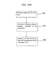
- FIG. 10A is a flow chart showing a method of manufacturing the barrier film composite of FIGS.1A to 1C ;
- FIG. 10B is a flow chart showing a method of manufacturing the barrier film composite of FIGS. 3A to 3C ;
- FIG. 11 is a flow chart showing a method of manufacturing the display apparatus of FIG. 2 .
- a film having multilayer barrier coating creates a barrier film with unsurpassed barrier performance is described in U.S. Patent No. 6,268,695 , entitled “Environmental Barrier Material For Organic Light Emitting Device And Method Of Making,” issued July 31, 2001; U.S. Patent No. 6,522,067 , entitled “Environmental Barrier Material For Organic Light Emitting Device And Method Of Making,” issued February 18, 2003; U.S. Patent No. 6,570,325 , entitled “Environmental Barrier Material For Organic Light Emitting Device And Method Of Making", issued May 27, 2003; U.S. Patent No. 6,866,901 , entitled “Method for Edge Sealing Barrier Films", issued March 15, 2005; U.S. Patent No.
- barrier stacks are not limited. The number of barrier stacks needed depends on the substrate material used and on the level of permeation resistance needed for the particular application. One or two barrier stacks may provide sufficient barrier properties for some applications. The most stringent applications may require five or more barrier stacks.
- the barrier stacks may include at least one decoupling layer and at least one barrier layer. There may be one decoupling layer and one barrier layer, there may be at least one decoupling layer disposed on one side of at least one barrier layer, there may be at least one decoupling layer disposed on both sides of at least one barrier layer, or there may be at least one barrier layer disposed on both sides of at least one decoupling layer.
- a barrier stack may include at least one decoupling layer and at least one barrier layer.
- the barrier layers in the barrier stacks may be made of the same material or of a different material as each other, and the decoupling layers may also be made of the same material or of a different material as each other.
- Each of the barrier layers may be typically about 100 to about 2000 ⁇ thick.
- a first barrier layer which is first formed among all barrier layers may be thicker than later barrier layers which are later formed among all barrier layers in comparison with the first barrier layer, if desired.
- the first barrier layer may have a thickness of about 1000 ⁇ to about 1500 ⁇ , while later barrier layers may have a thickness of about 400A to about 500 ⁇ .
- the first barrier layer may be thinner than later barrier layers.
- the first barrier layer may have a thickness of about 100 ⁇ to about 400 A, while later barrier layers may have a thickness of about 400 ⁇ to about 500 ⁇ .
- the decoupling layers may be typically about 0.1 to about 10 ⁇ m thick.
- the first decoupling layer may be thicker than later decoupling layers, if desired.
- the first decoupling layer which is first formed among all decoupling layers may have a thickness of about 3 ⁇ m to about 5 ⁇ m, while later decoupling layers which are later formed among all decoupling layers in comparison with the first decoupling layer may have a thickness of about 0.1 ⁇ m to about 2 ⁇ m.
- the barrier stacks may include the same or different layers, and the layers may be arranged in the same or different sequences.
- the decoupling layers may be made from the same decoupling material or different decoupling materials.
- the decoupling layers may be made of at least one selected from among, but not limited to, organic polymers, polymers including inorganic elements, organometallic polymers, hybrid organic/inorganic polymer systems, and combinations thereof.
- the organic polymers may be at least one selected from among, but not limited to, urethanes, polyamides, polyimides, polybutylenes, isobutylene isoprene, polyolefins, epoxies, parylenes, benzocyclobutadiene, polynorbornenes, polyarylethers, polycarbonates, alkyds, polyaniline, ethylene vinyl acetate, ethylene acrylic acid, and combinations thereof.
- urethanes polyamides, polyimides, polybutylenes, isobutylene isoprene, polyolefins, epoxies, parylenes, benzocyclobutadiene, polynorbornenes, polyarylethers, polycarbonates, alkyds, polyaniline, ethylene vinyl acetate, ethylene acrylic acid, and combinations thereof.
- the polymers including inorganic elements may be at least one selected from among, but not limited to, silicones, polyphosphazenes, polysilazanes, polycarbosilanes, polycarboranes, carborane siloxanes, polysilanes, phosphonitriles, sulfur nitride polymers, siloxanes, and combinations thereof.
- the organometallic polymers may be at least one selected from among, but not limited to, organometallic polymers of main group metals, transition metals, and lanthanide/actinide metals, and combinations thereof.
- the hybrid organic/inorganic polymer systems may be at least one selected from among, but not limited to, organically modified silicates, preceramic polymers, polyimide-silica hybrids, (meth)acrylate-silica hybrids, polydimethylsiloxane-silica hybrids, and combinations thereof.
- the barrier layers may be made from the same barrier material or different barrier materials.
- the barrier layers may be made of any suitable barrier material.
- Suitable inorganic materials based on metals may be at least selected from among, but not limited to, individual metals, two or more metals as mixtures, inter-metallics or alloys, metal and mixed metal oxides, metal and mixed metal fluorides, metal and mixed metal nitrides, metal and mixed metal carbides, metal and mixed metal carbonitrides, metal and mixed metal oxynitrides, metal and mixed metal borides, metal and mixed metal oxyborides, metal and mixed metal silicides, and combinations thereof.
- the metals may be at least one selected from among, not limited to, transition ("d” block) metals, lanthanide ("f” block) metals, aluminum, indium, germanium, tin, antimony and bismuth, and combinations thereof. Many of the resultant metal based materials will be conductors or semiconductors.
- the fluorides and oxides may be at least one selected from among, but not limited to, dielectrics (insulators), semiconductors and metallic conductors.
- the conductive oxides may be at least one selected from among, but not limited to, aluminum doped zinc oxide, indium tin oxide (ITO), antimony tin oxide, titanium oxides (TiO x where 0.8 ⁇ x ⁇ 1), and tungsten oxides (WO x where 2.7 ⁇ x ⁇ 3.0).
- Suitable inorganic materials based on "p" block semiconductors and non-metals may be at least one selected from among, but not limited to, silicon, silicon compounds, boron, boron compounds, carbon compounds including amorphous carbon and diamond-like carbon, and combinations thereof.
- the silicon compounds may be at least one selected from among, but not limited to, silicon oxides (SiO x where 1 ⁇ x ⁇ 2), polysilicic acids, alkali and alkaline earth silicates, aluminosilicates (Al x SiO y ), silicon nitrides (SN x H y where 0 ⁇ y ⁇ 1), silicon oxynitrides (SiN x O y H z where 0 ⁇ z ⁇ 1), silicon carbides (SiC x Hy where 0 ⁇ y ⁇ 1), and silicon aluminum oxynitrides (SiAlONs).
- the boron compounds may be at least one selected from among, but not limited to, boron carbides, boron nitrides, boron oxynitrides, boron carbonitrides, and combinations thereof.
- the barrier layers may be deposited by using any suitable process including, but not limited to, contemporary vacuum processes such as sputtering, evaporation, sublimation, chemical vapor deposition (CVD), plasma enhanced chemical vapor deposition (PECVD), electron cyclotron resonance-plasma enhanced vapor deposition (ECR-PECVD), and combinations thereof.
- CVD chemical vapor deposition
- PECVD plasma enhanced chemical vapor deposition
- ECR-PECVD electron cyclotron resonance-plasma enhanced vapor deposition
- the decoupling layers may be produced by using a number of known processes which provide improved surface planarity, including both atmospheric processes and vacuum processes.
- the decoupling layers may be formed by depositing a layer of liquid and subsequently processing the layer of liquid into a solid film. Depositing the decoupling layers as a liquid allows the liquid to flow over and to compensate the defects in the substrate or a previous layer, fill in lower areas, and cover up higher points, providing a surface with significantly improved planarity. When the decoupling layers are processed into a solid film, the improved surface planarity is retained.
- Suitable processes for depositing a layer of liquid material and processing it into a solid film include, but are not limited to, vacuum processes and atmospheric processes.
- Suitable vacuum processes include, but are not limited to, those described in U.S.
- Patent Nos. 5,260,095 , 5,395,644 , 5,547,508 , 5,691,615 , 5,902,641 , 5,440,446 , and 5,725,909 which are incorporated herein by reference.
- Liquid spreading apparatuses described in US Patent Nos. 5,260,095 , 5,395,644 , and 5,547,508 which are incorporated herein by reference, may be further configured to print liquid monomer in discrete, precisely placed regions of the receiving substrate.
- Suitable atmospheric processes include, but are not limited to, spin coating, printing, ink jet printing, and/or spraying.
- Atmospheric processes refer to processes that run at pressures of about 1 atmosphere and can employ the ambient atmosphere.
- the use of atmospheric processes presents a number of difficulties including the need to cycle between a vacuum environment for depositing the barrier layer and ambient conditions for the decoupling layer, and exposure of the environmentally sensitive device to environmental contaminants, such as oxygen and moisture.
- One way to alleviate these problems is to use a specific gas (purge gas) during the atmospheric process to control exposure of the receiving substrate to the environmental contaminants.
- the process may include cycling between a vacuum environment for barrier layer deposition and an ambient pressure nitrogen environment for the atmospheric process.
- Printing processes including ink jet printing, allow the deposition of the decoupling layer in a precise area without the use of masks.
- a decoupling layer involves depositing a polymer precursor, such as a (meth)acrylate containing polymer precursor, and then polymerizing it in situ to form the decoupling layer.
- a polymer precursor means a material which may be polymerized to form a polymer, including, but not limited to, monomers, oligomers, and resins.
- a preceramic precursor may be deposited as a liquid by spin coating and then be converted to a solid layer. Full thermal conversion is possible for a film of this type directly on a glass or oxide coated substrate.
- Electron beam techniques may be used to crosslink and/or densify some of these types of polymers and may be combined with thermal techniques to overcome some of the substrate thermal limitations, provided the substrate may handle the electron beam exposure.
- Another example of making a decoupling layer involves depositing a material, such as a polymer precursor, as a liquid at a temperature above its melting point and subsequently freezing it in place.
- One method of making a barrier film composite includes providing a substrate, and depositing a barrier layer adjacent to the substrate at a barrier deposition station.
- the substrate with the barrier layer may be moved to a decoupling material deposition station.
- a mask is provided with an opening which limits the deposition of the decoupling layer to an area which is smaller than, and contained within, the area covered by the barrier layer.
- the first layer deposited may be either the barrier layer or the decoupling layer, depending on the design of the composite.
- These multilayer, barrier coatings and barrier films are relatively flexible. These multilayer, barrier coatings and barrier films typically start cracking only when they are wrapped over a 7 mm radius spindle. For example, the thin (about 60 nm) aluminum oxide barrier layers in the barrier coating start showing cracks around a 0.75% tensile strain. While optimization of the adhesion and materials might be able to shift the threshold of first cracks to higher values, it is unlikely that such a multilayer barrier film could be stretched to several percent elongation.
- the pristine multilayer barrier film has been shown to be almost stress free (the tensile stress of the aluminum oxide layers is only 470 MPa, and the tensile stress of the polymers layers is even lower), resulting in processed films which are flat and which do not curl under heat treatment.
- the barrier properties of the pristine multilayer barrier films have been shown to have a water vapor transmission rate (WVTR) of 1x10 -6 g/m 2 /day.
- stretchable barrier films may be to protect a wide range of environmentally sensitive materials and objects, ranging from flexible displays and solar cells to car bumpers used for corrosion protection and medical applications.
- a moldable coating which may be wrapped on the object (e.g., a car bumper) without the manufacturing company having to conduct wet processing with environmentally unfriendly chemicals and having to deal with the resulting contaminant and waste effluent problems.
- stretchable barrier film composites is to be used as a barrier coating on the exterior of a three dimensional object, which may be created by putting a barrier film in a mold and injecting plastic into the mold.
- One aspect of the invention is either to prevent barrier layers from cracking or to minimize and compensate for cracks.
- the resulting barrier might not meet a WVTR of 1x10 -6 g/m 2 /day, but it may still have a good WVTR that is about 100 times better than a homogenous barrier film such as a polychlorotrifluoroethylene film (e.g., ACLAR ® film available from Honeywell International, Inc.).
- a homogenous barrier film such as a polychlorotrifluoroethylene film (e.g., ACLAR ® film available from Honeywell International, Inc.).
- FIGS. 1A to 1C illustrate a barrier film composite 1 and a method of manufacturing the barrier film composite 1, according to an embodiment of the present invention.
- a mold 105 is provided with an undulating surface.
- the mold 105 having the undulating surface 110 may be formed by performing embossing or photolithography on an original mold having a flat surface.
- Decoupling layers 115 and barrier layers 120 may be alternately formed to conform to the surface of the mold 105.
- the decoupling layers 115 and the barrier layers 120 form a very soft, elastic undulating structure, which is stretchable.
- a decoupling layer 115 is coated on the surface 110 of the mold 105, and a barrier layer 120 is then sputtered over and conforms to the decoupling layer 115.
- FIGS. 1A to 1C illustrate that the decoupling layer 115 is directly disposed on the surface 110 of the mold 105, the deposition order of the decoupling layer 115 and the barrier layer 120 may be reversed.
- the decoupling layers 115 may include, but are not limited to, cross-linked acrylates with low glass transition temperatures (Tg), for example, ranging from about -80°C to about 40°C. This process may be repeated as many times as necessary, forming alternating layers of decoupling layers 115 and barrier layers 120 conforming to one another.
- Tg glass transition temperatures
- a film 125 may be laminated on a surface of the alternating decoupling layers 115 and barrier layers 120.
- the film 125 also has an undulating surface due to the undulating structure of the decoupling layers 115 and barrier layers 120.
- the film 125 may be formed from a stretchable material.
- the film 125 has a stretchable structure.
- the film 125 may include, but is not limited to, at least one selected from among polyethylene, polypropylene, polycarbonate, and combinations thereof.
- the mold 105 is released from a barrier film composite 1 that includes the alternating layers of decoupling layers 115 and barrier layers 120, and the film 120.
- the adhesion between the surface 110 of the mold 105 and the layer in direct contact with the surface 110 may be weaker than the adhesion between the film 125 and the alternating layers of decoupling layers 115 and barrier layers 120.
- the barrier film composite 1, including the alternating layers of decoupling layers 115 and barrier layers 120, released from the mold 105 may provide a very soft, elastic polymer-based structure with an undulating surface.
- the undulating structure is created using molding with the mold 105, thereby alleviating environmental problems.
- FIG. 10A is a flow chart showing a method of manufacturing the barrier film composite according one embodiment.
- the method may include steps of providing a mold having an undulating surface (S10), disposing at least one decoupling layer and at least one barrier layer having an undulating structure on the undulating surface of the mold (S11), laminating a film on a surface of the alternating decoupling layers and barrier layers (S12), and removing the mold (S 13).
- the film may have a flat exposed surface.
- FIG. 2 illustrates an organic light-emitting display apparatus 100 including the barrier film composite 1 of FIG. 1C , according to an embodiment of the present invention.
- the barrier film composite 1 may be used with environmentally sensitive materials or objects, and may be used in a flexible display apparatus.
- Organic light-emitting display apparatuses include organic emission layers that are vulnerable to oxygen and moisture, and there is also an increasing demand for flexible display apparatuses as next-generation display apparatuses.
- the organic light-emitting display apparatus 100 includes an organic light-emitting device 20 on a surface of a substrate 10, and the barrier film composite 1, which encapsulates the organic light-emitting device 20.
- FIG. 2 illustrates an suitable application of the barrier film composite 1 as an encapsulating material for the organic light-emitting device 20, aspects of the present invention are not limited thereto.
- the barrier film composite 1 may also be used as the substrate 10.
- the substrate 10 may include a flexible material, such as plastics or polyimides.
- the organic light-emitting device 20 includes a first electrode layer 21, an organic emission layer 23, and a second electrode layer 25.
- the first electrode layer 21 and the second electrode layer 25 may be used as either an anode or a cathode, and may each be used as one of a reflective electrode, a transparent electrode, and a semi-transparent electrode.
- the organic emission layer 23 may include a low-molecular weight organic material or a large-molecular weight organic material.
- a hole transport layer (HTL) and a hole injection layer (HIL) may be sequentially disposed on a surface of the organic emission layer 23, and an electron transport layer (ETL) and an electron injection layer (EIL) may be sequentially disposed on the opposite surface thereof.
- ETL electron transport layer
- EIL electron injection layer
- Suitable low-molecular weight organic materials include copper phthalocyanine (CuPc), N'-di(naphthalene-1-yl)-N, N'-diphenyl-benzidine (NPB), tris-8-hydroxyquinoline aluminum (Alq3), and the like.
- a HTL may be further included, in addition to the organic emission layer 23.
- the HTL may be formed from poly-(2,4)-ethylene-dihydroxy thiophene (PEDOT), polyaniline (PANI), or the like.
- suitable large-molecular weight organic materials include polyphenylenevinylenes (PPV), polyfluorenes, and the like.
- the organic light-emitting display device 100 including the barrier film composite 1 as described above may have a soft, elastic structure, enabling the manufacture of a flexible display.
- the barrier film composite 1 does not crack or is less likely to crack, and thus may protect the organic emission layer 23 from external moisture and oxygen.
- the organic light-emitting display apparatus 100 may further include the layer 30 which is disposed between the organic light-emitting device 20 and the barrier film composite 1.
- the layer 30 may be a flexible layer which may deform in order to confirm to the undulating surface of the decoupling layer 115.
- the barrier film composite 1 may be used in various types of display apparatuses.
- FIG. 11 is a flow chart showing a method of manufacturing an OLED device. This method includes steps of providing a first substrate comprised of a barrier film composite including at least one decoupling layer and at least one barrier layer disposed on a surface of the film (S30), providing a second substrate on which a light-emitting device is disposed (S31), and coupling the first and second substrates (S32).
- FIGS. 3A to 3C illustrate a barrier film composite 2 and a method of manufacturing the barrier film composite 2, according to another embodiment of the present invention.
- a second layer 145 is formed on a first layer 140, and parts thereof are subjected to first irradiation (L1).
- the first layer 140 may include a flexible material, such as plastic.
- the second layer 145 may include a soft monomer with a low glass transition temperatures (Tg). Suitable soft monomers may include longer-chain alkyl acrylates, such as n-butyl acrylate, 2-ethyl hexyl acrylate, and iso-octyl acrylate.
- the first irradiation L1 may be laser writing, or irradiation through a mask.
- the second layer 145 has an undulating surface 150.
- One surface of the second layer 145 exposed to the first irradiation (L1) partially shrinks or expands resulting in an undulating surface, and the one surface of the second layer 145 is then fixed and firmed and consolidated by a second irradiation (not shown), resulting in the undulating surface 150.
- alternating layers of decoupling layers 115 and barrier layers 120 are laminated on the undulating surface 150 of the second layer 145, as in the previous embodiment described above.
- the undulating surface 150 of the second layer 145 is transferred to the alternating layers of decoupling layers 115 and barrier layers 120, causing one surface thereof to undulate.
- the undulating structure is created with light irradiation as described above, thereby alleviating environmental problems.
- FIG. 10B is a flow chart showing a method of manufacturing the barrier film composite according another embodiment.
- the method includes steps of forming a second layer on a first layer (S20), forming an undulating surface by applying irradiation on the second layer (S21), and depositing at least one barrier layer and decoupling layer on the undulating surface (S22).
- FIG. 4 illustrates a barrier film composite 3 according to another embodiment of the present invention.
- bubbles of polymer material 310 are surrounded by barrier material 315.
- the polymer material 310 is soft and stretchable. When stretched, most of the bubbles will elongate, but not break. While some bubbles may break, this will not provide a direct path to the outside because the break may be covered by other bubbles.
- FIGS. 5A and 5B illustrate barrier film composites 4-1 and 4-2, respectively, according to other embodiments of the present invention.
- the barrier film composite 4-1 includes double barrier layers 405 and 410.
- the double barrier layers 405 and 410 are spaced apart from each other by a thin layer (about 10 nm to about 100 nm thick) of rubbery stretchable polymer 415.
- Suitable rubbery stretchable polymers include, but are not limited to, cross-linked acrylates with low Tg.
- the barrier film composite 4-2 may include a getter material 420 dispersing within the polymer layer 415.
- the particle size (diameter) of the getter material 420 may be on a nanometer scale, for example, may be from about Inm to about 100 nm.
- the rubbery, stretchable polymer layer 415 may contain inorganic oxide or nitride particles to create a tortuous path for moisture.
- FIG. 6 illustrates a barrier film composite 5 according to another embodiment of the present invention.
- the barrier film composite 5 includes alternating layers of inorganic barrier layers 505 and decoupling layers 510. Each of the inorganic barrier layers 505 is covered by a thin layer of getter material 515. When stretched, the inorganic barrier layers 505 may crack, but the getter layer 515 will reduce the impact of the cracks.
- FIG. 7 illustrates a barrier film composite 6 according to another embodiment of the present invention.
- the barrier film composite 6 includes alternating layers of barrier layers 605 and decoupling layers 610.
- the barrier materials 605 may include inorganic materials, and in some embodiments, may include at least one material selected from among individual metals, two or more metals as mixtures, inter-metallics or alloys, metal and mixed metal oxides, metal and mixed metal fluorides, metal and mixed metal nitrides, metal and mixed metal carbides, metal and mixed metal carbonitrides, metal and mixed metal oxynitrides, metal and mixed metal borides, metal and mixed metal oxyborides, metal and mixed metal silicides, and combinations thereof, as listed above.
- Each of the barrier layers 605 includes a first region 615, and a second region 620 that has thinner thickness in comparison with the first region 615.
- the second region 620 has less mechanical strength in comparison with the first region 615. When the barrier film composite 6 is stretched, the second region 620 alleviates stress and helps the barrier film composite 6 elongate.
- the first region 615 and the second region 620 may be formed from the same material. In one embodiment the first region 615 and the second region 620 may be formed from different materials. For example, the second region 620 may include a material having smaller mechanical strength in comparison with a material forming the first region 615.
- the second region 620 may have varying thicknesses. As illustrated in FIG. 7 , the thickness of the second region 620 may decrease toward a center of the second region 620 from sides of the second region 620 with a wedged cross-section. However, aspects of the present invention are not limited thereto.
- Each of the barrier layers 605 may include a plurality of second regions 620.
- a pitch between each two adjacent second regions 620 may be same.
- aspects of the present invention are not limited thereto.
- the plurality of second regions 620 may be formed with a shadow mask. However, aspects of the present invention are not limited thereto.
- each barrier layer 605 may be positioned so as not to overlap with those in adjacent barrier layers 605.
- the barrier layers 605, including the second regions 620 may reduce the impact of the cracks, since the pitch P between each two adjacent second regions 620 in each barrier layer 605 is also extended, thereby elongating potential external contamination paths, which may be formed by the second regions 620.
- FIG. 8 illustrates an organic light-emitting display apparatus 200 including the barrier film composite 6 of FIG. 7 , according to another embodiment of the present invention.
- the organic light-emitting display apparatus 200 includes an organic light-emitting device 20 on a surface of a substrate 10, and the barrier film composite 6, which encapsulates the organic light-emitting device 20.
- FIG. 8 illustrates a suitable application of the barrier film composite 6 as an encapsulating material for the organic light-emitting device 20, aspects of the present invention are not limited thereto.
- the barrier film composite 6 may also be used as the substrate 10.
- the substrate 10 may include a flexible material, such as plastics or polyimides.
- the organic light-emitting device 20 includes a first electrode layer 21, an organic emission layer 23, and a second electrode layer 25. A detailed description of the organic light-emitting device 20 will not be provided here, since it has already been described above in connection with the organic light-emitting display apparatus 100 of FIG. 2 .
- the organic light-emitting display device 200 including the barrier film composite 6 as described above may have a soft, elastic structure, enabling the manufacture of a flexible display.
- the barrier film composite 6 is less likely to crack, and thus may protect the organic emission layer 23 from external moisture and oxygen, even when cracking occurs, due to the pitch P extending between the second regions 620 and potential external contamination paths are elongated as the barrier film composite 6 is stretched.
- the organic light-emitting display apparatus 200 may further include the layer 30 which is disposed between the organic light-emitting device 20 and the barrier film composite 6.
- the layer 30 may be a flexible layer.
- FIG. 9 illustrates a barrier film composite 7 according to another embodiment of the present invention.
- the barrier film composite 7 includes alternating layers of inorganic barrier layers 710 and decoupling layers 715 alternatingly disposed on a substrate 705.
- Metal ribs 720 may be disposed in the inorganic barrier layers 710, if partial loss of transparency is acceptable. Suitable materials for the metal ribs 720 include, but are not limited to, soft metals, alloys, tin (Sn), indium (In), and combinations thereof. The metal ribs 720 can be stretched without breaking. The metal ribs 720 may be two-dimensional.
- barrier film composites Another method of making barrier film composites involves making the inorganic barrier layers out of a very ductile soft metal or metal alloy, such as tin.
- the multilayer structure will be semitransparent or even opaque, depending on the thickness and number of layers used. There are however many applications for the stretchable multilayer barrier which do not require a transparent barrier.
- barrier film composites Another method of making barrier film composites is to cover the inorganic barrier layers with a thin layer of nanoparticles of an inorganic oxide or nitride.
- the inorganic barrier layer may crack when it is stretched, but the nanoparticles should reduce the effect of the cracks by increasing the length of the undulating path.
- barrier film composites Another method of making barrier film composites is to stretch a soft substrate and deposit the inorganic barrier layers on the substrate while the soft substrate is being stretched. When the tension is released, the inorganic barrier layer will be compressed. This will allow some stretching of the inorganic layers when the structure is used.
- a stretchable barrier film composite provides a soft, elastic polymer-based structure with an undulating surface, and a display apparatus may be manufactured using the flexible barrier film composite.
Abstract
Description
- The present invention relates to a barrier film composite, a display apparatus including the same, a method of manufacturing the barrier film composite, and a method of manufacturing the display apparatus including the barrier film composite.
- Multilayered thin film barrier composites having alternating layers of barrier material and decoupling material are well known. These barrier composites are typically formed by depositing alternating layers of barrier material and decoupling material, for example, by vapor deposition. Each of the barrier layers is typically a few hundred Angstroms thick, while each of the decoupling layers is generally less than ten microns thick.
- There is demand for stretchable multilayer barrier film composites, methods of forming such composites, display apparatuses including such a barrier film composite, and methods of manufacturing display apparatuses including such a barrier film composite.
- Embodiments of the present invention provide a stretchable barrier film composite, a display apparatus including the stretchable barrier film, and methods of manufacturing the barrier film composite and the display apparatus including the barrier film composite.
- In accordance with an aspect of the present invention, a barrier film composite may include a film with an undulating surface; and at least one decoupling layer and at least one barrier layer disposed on a surface of the film.
- The film may include a stretchable material.
- The film may include at least one selected from the group consisting of polyethylene, polypropylene, polycarbonate, and combinations thereof.
- The film may include a first layer that is stretchable, and a second layer disposed on the first layer with an undulating surface.
- The first layer may include plastic, and the second layer may include a soft monomer.
- The barrier film composite may include alternating layers of the at least one decoupling layer and at least one barrier layer.
- The at least one decoupling layer may include a cross-linked material with a low glass transition temperature.
- The decoupling layer may include an acrylate.
- The barrier layer may include at least one selected from the group consisting of individual metals, two or more metals as mixtures, inter-metallics or alloys, metal and mixed metal oxides, metal and mixed metal fluorides, metal and mixed metal nitrides, metal and mixed metal carbides, metal and mixed metal carbonitrides, metal and mixed metal oxynitrides, metal and mixed metal borides, metal and mixed metal oxyborides, metal and mixed metal silicides, and combinations thereof.
- In accordance with another aspect of the present invention, a display apparatus may include a first substrate; a second substrate disposed opposite to and spaced apart from the first substrate; and a light-emitting device between the first substrate and the second substrate, wherein at least one of the first substrate and the second substrate includes the barrier film composite of any one of the embodiments described above.
- The light-emitting device may include an organic light-emitting device.
- In accordance with another aspect of the present invention, a method of manufacturing a barrier film composite may include steps of providing a film having an undulating surface; and disposing at least one decoupling layer and at least one barrier layer having an undulating structure on a surface of the film.
- The method may further include providing a mold having an undulating surface, wherein at least one decoupling layer and at least one barrier layer are formed on the undulating surface of the mold, and a film is formed on a surface of the at least one decoupling layer and at least one barrier layer.
- The mold with the undulating surface may be formed by applying embossing or photolithography on an original mold having a flat surface.
- The adhesion between the undulating surface of the mold and either the decoupling layer or the barrier layer that is in direct contact with the mold may be weaker than the adhesion between the film and the surface of the decoupling layer and barrier layer that is in direct contact with the film.
- The method may further include releasing the mold from the decoupling layer and the barrier layer, after the forming of the film.
- The providing of the film may include forming a first layer; and forming a second layer on the first layer. The combination of the first and second layers are subjected by an irradiation in order to obtain an undulating surface of the second layer.
- The first irradiation may include laser writing or irradiation through a mask.
- The method may further include fixing and firming the undulating surface of the second layer by a second irradiation.
- In accordance with another aspect of the present invention, a method of manufacturing a display apparatus including the barrier film composite of any one of the embodiments described above, may include steps of providing a first substrate and a second substrate opposite to and spaced apart from each other; and disposing a light-emitting device between the first substrate and the second substrate.
- The light-emitting device may include an organic light-emitting device.
- At least some of the above and other features of the invention are set out in the appended claims.
- A more complete appreciation of the invention, and many of the attendant advantages thereof, will be readily apparent as the same becomes better understood by reference to the following detailed description when considered in conjunction with the accompanying drawings in which like reference symbols indicate the same or similar components, wherein:
-
FIGS. 1A to 1C are cross sectional views illustrating a barrier film composite and a method of manufacturing the barrier film composite, according to an embodiment of the present invention; -
FIG. 2 is a cross sectional view illustrating an organic light-emitting display apparatus including the barrier film composite ofFIG. 1C , according to an embodiment of the present invention; -
FIGS. 3A to 3C are cross sectional views illustrating a barrier film composite and a method of manufacturing the barrier film composite, according to another embodiment of the present invention; -
FIG. 4 is a cross sectional view illustrating a barrier film composite constructed as another embodiment of the present invention; -
FIG 5A and 5B are cross sectional views illustrating barrier film composites constructed as other embodiments of the present invention; -
FIG. 6 is a cross sectional view illustrating a barrier film composite constructed as another embodiment of the present invention; -
FIG. 7 is a cross sectional view illustrating a barrier film composite constructed as another embodiment of the present invention; -
FIG. 8 is a cross sectional view illustrating an organic light-emitting display apparatus including the barrier film composite ofFIG. 7 , according to an embodiment of the present invention; -
FIG. 9 is a cross sectional view illustrating a barrier film composite constructed as another embodiment of the present invention; -
FIG. 10A is a flow chart showing a method of manufacturing the barrier film composite ofFIGS.1A to 1C ; -
FIG. 10B is a flow chart showing a method of manufacturing the barrier film composite ofFIGS. 3A to 3C ; and -
FIG. 11 is a flow chart showing a method of manufacturing the display apparatus ofFIG. 2 . - A film having multilayer barrier coating creates a barrier film with unsurpassed barrier performance, is described in
U.S. Patent No. 6,268,695 , entitled "Environmental Barrier Material For Organic Light Emitting Device And Method Of Making," issued July 31, 2001;U.S. Patent No. 6,522,067 , entitled "Environmental Barrier Material For Organic Light Emitting Device And Method Of Making," issued February 18, 2003;U.S. Patent No. 6,570,325 , entitled "Environmental Barrier Material For Organic Light Emitting Device And Method Of Making", issued May 27, 2003;U.S. Patent No. 6,866,901 , entitled "Method for Edge Sealing Barrier Films", issued March 15, 2005;U.S. Patent No. 7,198,832 , entitled "Method for Edge Sealing Barrier Films", issued April 3, 2007;U.S. Patent Application Serial No. 11/068,356 , entitled "Method for Edge Sealing Barrier Films", filed February 28, 2005;U.S. Patent Application Serial No. 11/693,020 U.S. Patent Application Serial No. 11/693,022 U.S. Patent Application Serial No. 11/776616 - The number of barrier stacks is not limited. The number of barrier stacks needed depends on the substrate material used and on the level of permeation resistance needed for the particular application. One or two barrier stacks may provide sufficient barrier properties for some applications. The most stringent applications may require five or more barrier stacks.
- The barrier stacks may include at least one decoupling layer and at least one barrier layer. There may be one decoupling layer and one barrier layer, there may be at least one decoupling layer disposed on one side of at least one barrier layer, there may be at least one decoupling layer disposed on both sides of at least one barrier layer, or there may be at least one barrier layer disposed on both sides of at least one decoupling layer. A barrier stack may include at least one decoupling layer and at least one barrier layer. The barrier layers in the barrier stacks may be made of the same material or of a different material as each other, and the decoupling layers may also be made of the same material or of a different material as each other.
- Each of the barrier layers may be typically about 100 to about 2000 Å thick. In some embodiments a first barrier layer which is first formed among all barrier layers may be thicker than later barrier layers which are later formed among all barrier layers in comparison with the first barrier layer, if desired. For example, the first barrier layer may have a thickness of about 1000Å to about 1500Å, while later barrier layers may have a thickness of about 400A to about 500 Å. In some other embodiments, the first barrier layer may be thinner than later barrier layers. For example, the first barrier layer may have a thickness of about 100 Å to about 400 A, while later barrier layers may have a thickness of about 400 Å to about 500 Å. The decoupling layers may be typically about 0.1 to about 10 µm thick. In some embodiments the first decoupling layer may be thicker than later decoupling layers, if desired. For example, the first decoupling layer which is first formed among all decoupling layers may have a thickness of about 3 µm to about 5 µm, while later decoupling layers which are later formed among all decoupling layers in comparison with the first decoupling layer may have a thickness of about 0.1 µm to about 2 µm.
- The barrier stacks may include the same or different layers, and the layers may be arranged in the same or different sequences.
- The decoupling layers may be made from the same decoupling material or different decoupling materials. The decoupling layers may be made of at least one selected from among, but not limited to, organic polymers, polymers including inorganic elements, organometallic polymers, hybrid organic/inorganic polymer systems, and combinations thereof. The organic polymers may be at least one selected from among, but not limited to, urethanes, polyamides, polyimides, polybutylenes, isobutylene isoprene, polyolefins, epoxies, parylenes, benzocyclobutadiene, polynorbornenes, polyarylethers, polycarbonates, alkyds, polyaniline, ethylene vinyl acetate, ethylene acrylic acid, and combinations thereof. The polymers including inorganic elements may be at least one selected from among, but not limited to, silicones, polyphosphazenes, polysilazanes, polycarbosilanes, polycarboranes, carborane siloxanes, polysilanes, phosphonitriles, sulfur nitride polymers, siloxanes, and combinations thereof. The organometallic polymers may be at least one selected from among, but not limited to, organometallic polymers of main group metals, transition metals, and lanthanide/actinide metals, and combinations thereof. The hybrid organic/inorganic polymer systems may be at least one selected from among, but not limited to, organically modified silicates, preceramic polymers, polyimide-silica hybrids, (meth)acrylate-silica hybrids, polydimethylsiloxane-silica hybrids, and combinations thereof.
- The barrier layers may be made from the same barrier material or different barrier materials. The barrier layers may be made of any suitable barrier material. Suitable inorganic materials based on metals may be at least selected from among, but not limited to, individual metals, two or more metals as mixtures, inter-metallics or alloys, metal and mixed metal oxides, metal and mixed metal fluorides, metal and mixed metal nitrides, metal and mixed metal carbides, metal and mixed metal carbonitrides, metal and mixed metal oxynitrides, metal and mixed metal borides, metal and mixed metal oxyborides, metal and mixed metal silicides, and combinations thereof. The metals may be at least one selected from among, not limited to, transition ("d" block) metals, lanthanide ("f" block) metals, aluminum, indium, germanium, tin, antimony and bismuth, and combinations thereof. Many of the resultant metal based materials will be conductors or semiconductors. The fluorides and oxides may be at least one selected from among, but not limited to, dielectrics (insulators), semiconductors and metallic conductors. The conductive oxides may be at least one selected from among, but not limited to, aluminum doped zinc oxide, indium tin oxide (ITO), antimony tin oxide, titanium oxides (TiOx where 0.8 ≤ x ≤ 1), and tungsten oxides (WOx where 2.7 ≤ x < 3.0). Suitable inorganic materials based on "p" block semiconductors and non-metals may be at least one selected from among, but not limited to, silicon, silicon compounds, boron, boron compounds, carbon compounds including amorphous carbon and diamond-like carbon, and combinations thereof. The silicon compounds may be at least one selected from among, but not limited to, silicon oxides (SiOx where 1 ≤ x ≤ 2), polysilicic acids, alkali and alkaline earth silicates, aluminosilicates (AlxSiOy), silicon nitrides (SNxHy where 0 ≤ y ≤ 1), silicon oxynitrides (SiNxOyHz where 0 ≤ z ≤ 1), silicon carbides (SiCxHy where 0 ≤ y ≤ 1), and silicon aluminum oxynitrides (SiAlONs). The boron compounds may be at least one selected from among, but not limited to, boron carbides, boron nitrides, boron oxynitrides, boron carbonitrides, and combinations thereof.
- The barrier layers may be deposited by using any suitable process including, but not limited to, contemporary vacuum processes such as sputtering, evaporation, sublimation, chemical vapor deposition (CVD), plasma enhanced chemical vapor deposition (PECVD), electron cyclotron resonance-plasma enhanced vapor deposition (ECR-PECVD), and combinations thereof.
- The decoupling layers may be produced by using a number of known processes which provide improved surface planarity, including both atmospheric processes and vacuum processes. The decoupling layers may be formed by depositing a layer of liquid and subsequently processing the layer of liquid into a solid film. Depositing the decoupling layers as a liquid allows the liquid to flow over and to compensate the defects in the substrate or a previous layer, fill in lower areas, and cover up higher points, providing a surface with significantly improved planarity. When the decoupling layers are processed into a solid film, the improved surface planarity is retained. Suitable processes for depositing a layer of liquid material and processing it into a solid film include, but are not limited to, vacuum processes and atmospheric processes. Suitable vacuum processes include, but are not limited to, those described in
U.S. Patent Nos. 5,260,095 ,5,395,644 ,5,547,508 ,5,691,615 ,5,902,641 ,5,440,446 , and5,725,909 , which are incorporated herein by reference. Liquid spreading apparatuses described inUS Patent Nos. 5,260,095 ,5,395,644 , and5,547,508 , which are incorporated herein by reference, may be further configured to print liquid monomer in discrete, precisely placed regions of the receiving substrate. - Suitable atmospheric processes include, but are not limited to, spin coating, printing, ink jet printing, and/or spraying. Atmospheric processes refer to processes that run at pressures of about 1 atmosphere and can employ the ambient atmosphere. The use of atmospheric processes presents a number of difficulties including the need to cycle between a vacuum environment for depositing the barrier layer and ambient conditions for the decoupling layer, and exposure of the environmentally sensitive device to environmental contaminants, such as oxygen and moisture. One way to alleviate these problems is to use a specific gas (purge gas) during the atmospheric process to control exposure of the receiving substrate to the environmental contaminants. For example, the process may include cycling between a vacuum environment for barrier layer deposition and an ambient pressure nitrogen environment for the atmospheric process. Printing processes, including ink jet printing, allow the deposition of the decoupling layer in a precise area without the use of masks.
- One way to make a decoupling layer involves depositing a polymer precursor, such as a (meth)acrylate containing polymer precursor, and then polymerizing it in situ to form the decoupling layer. As used herein, the term "polymer precursor" means a material which may be polymerized to form a polymer, including, but not limited to, monomers, oligomers, and resins. As another example of a method of making a decoupling layer, a preceramic precursor may be deposited as a liquid by spin coating and then be converted to a solid layer. Full thermal conversion is possible for a film of this type directly on a glass or oxide coated substrate. Although the preceramic precursor sometimes cannot be fully converted to a ceramic at temperatures compatible with some flexible substrates, partial conversion to a cross-lined network structure would be satisfactory. Electron beam techniques may be used to crosslink and/or densify some of these types of polymers and may be combined with thermal techniques to overcome some of the substrate thermal limitations, provided the substrate may handle the electron beam exposure. Another example of making a decoupling layer involves depositing a material, such as a polymer precursor, as a liquid at a temperature above its melting point and subsequently freezing it in place.
- One method of making a barrier film composite includes providing a substrate, and depositing a barrier layer adjacent to the substrate at a barrier deposition station. The substrate with the barrier layer may be moved to a decoupling material deposition station. A mask is provided with an opening which limits the deposition of the decoupling layer to an area which is smaller than, and contained within, the area covered by the barrier layer. The first layer deposited may be either the barrier layer or the decoupling layer, depending on the design of the composite.
- These multilayer, barrier coatings and barrier films are relatively flexible. These multilayer, barrier coatings and barrier films typically start cracking only when they are wrapped over a 7 mm radius spindle. For example, the thin (about 60 nm) aluminum oxide barrier layers in the barrier coating start showing cracks around a 0.75% tensile strain. While optimization of the adhesion and materials might be able to shift the threshold of first cracks to higher values, it is unlikely that such a multilayer barrier film could be stretched to several percent elongation.
- The pristine multilayer barrier film has been shown to be almost stress free (the tensile stress of the aluminum oxide layers is only 470 MPa, and the tensile stress of the polymers layers is even lower), resulting in processed films which are flat and which do not curl under heat treatment.
- The barrier properties of the pristine multilayer barrier films have been shown to have a water vapor transmission rate (WVTR) of 1x10⁻⁶ g/m2/day.
- The application of such stretchable barrier films may be to protect a wide range of environmentally sensitive materials and objects, ranging from flexible displays and solar cells to car bumpers used for corrosion protection and medical applications.
- Instead of applying a wet or spray coating to a three dimensional object (paint for instance), more and more industries prefer a moldable coating which may be wrapped on the object (e.g., a car bumper) without the manufacturing company having to conduct wet processing with environmentally unfriendly chemicals and having to deal with the resulting contaminant and waste effluent problems.
- Another application of stretchable barrier film composites is to be used as a barrier coating on the exterior of a three dimensional object, which may be created by putting a barrier film in a mold and injecting plastic into the mold.
- Medical packaging for individual pills pockets using the multilayer barrier film is another potential application of stretchable barrier film composites.
- There are a number of ways to realize such structures. These methods make use of the flexibility of the barrier layer or take into account that the barrier layers break on stretching.
- One aspect of the invention is either to prevent barrier layers from cracking or to minimize and compensate for cracks. The resulting barrier might not meet a WVTR of 1x10⁻⁶ g/m2/day, but it may still have a good WVTR that is about 100 times better than a homogenous barrier film such as a polychlorotrifluoroethylene film (e.g., ACLAR® film available from Honeywell International, Inc.).
-
FIGS. 1A to 1C illustrate abarrier film composite 1 and a method of manufacturing thebarrier film composite 1, according to an embodiment of the present invention. - Referring
FIG. 1A , amold 105 is provided with an undulating surface. Themold 105 having the undulatingsurface 110 may be formed by performing embossing or photolithography on an original mold having a flat surface. - Decoupling layers 115 and
barrier layers 120 may be alternately formed to conform to the surface of themold 105. The decoupling layers 115 and the barrier layers 120 form a very soft, elastic undulating structure, which is stretchable. In particular, adecoupling layer 115 is coated on thesurface 110 of themold 105, and abarrier layer 120 is then sputtered over and conforms to thedecoupling layer 115. AlthoughFIGS. 1A to 1C illustrate that thedecoupling layer 115 is directly disposed on thesurface 110 of themold 105, the deposition order of thedecoupling layer 115 and thebarrier layer 120 may be reversed. The decoupling layers 115 may include, but are not limited to, cross-linked acrylates with low glass transition temperatures (Tg), for example, ranging from about -80°C to about 40°C. This process may be repeated as many times as necessary, forming alternating layers of decoupling layers 115 andbarrier layers 120 conforming to one another. - Referring to
FIG. 1B , afilm 125 may be laminated on a surface of the alternatingdecoupling layers 115 and barrier layers 120. Thefilm 125 also has an undulating surface due to the undulating structure of the decoupling layers 115 and barrier layers 120. Thefilm 125 may be formed from a stretchable material. Thus, thefilm 125 has a stretchable structure. Thefilm 125 may include, but is not limited to, at least one selected from among polyethylene, polypropylene, polycarbonate, and combinations thereof. - Referring to
FIG. 1C , themold 105 is released from abarrier film composite 1 that includes the alternating layers of decoupling layers 115 andbarrier layers 120, and thefilm 120. In order to facilitate the release of themold 105 from thebarrier film composite 1, the adhesion between thesurface 110 of themold 105 and the layer in direct contact with thesurface 110 may be weaker than the adhesion between thefilm 125 and the alternating layers of decoupling layers 115 and barrier layers 120. - As a result, the
barrier film composite 1, including the alternating layers of decoupling layers 115 andbarrier layers 120, released from themold 105 may provide a very soft, elastic polymer-based structure with an undulating surface. Instead of using wet or spay coating, the undulating structure is created using molding with themold 105, thereby alleviating environmental problems. -
FIG. 10A is a flow chart showing a method of manufacturing the barrier film composite according one embodiment. The method may include steps of providing a mold having an undulating surface (S10), disposing at least one decoupling layer and at least one barrier layer having an undulating structure on the undulating surface of the mold (S11), laminating a film on a surface of the alternating decoupling layers and barrier layers (S12), and removing the mold (S 13). The film may have a flat exposed surface. -
FIG. 2 illustrates an organic light-emittingdisplay apparatus 100 including thebarrier film composite 1 ofFIG. 1C , according to an embodiment of the present invention. - As described above, the
barrier film composite 1 may be used with environmentally sensitive materials or objects, and may be used in a flexible display apparatus. Organic light-emitting display apparatuses include organic emission layers that are vulnerable to oxygen and moisture, and there is also an increasing demand for flexible display apparatuses as next-generation display apparatuses. - Referring to
FIG. 2 , the organic light-emittingdisplay apparatus 100 includes an organic light-emittingdevice 20 on a surface of asubstrate 10, and thebarrier film composite 1, which encapsulates the organic light-emittingdevice 20. AlthoughFIG. 2 illustrates an suitable application of thebarrier film composite 1 as an encapsulating material for the organic light-emittingdevice 20, aspects of the present invention are not limited thereto. Thebarrier film composite 1 may also be used as thesubstrate 10. When thebarrier film composite 1 is used only to encapsulate the organic light-emittingdevice 20, thesubstrate 10 may include a flexible material, such as plastics or polyimides. - The organic light-emitting
device 20 includes afirst electrode layer 21, anorganic emission layer 23, and asecond electrode layer 25. - The
first electrode layer 21 and thesecond electrode layer 25 may be used as either an anode or a cathode, and may each be used as one of a reflective electrode, a transparent electrode, and a semi-transparent electrode. - The
organic emission layer 23 may include a low-molecular weight organic material or a large-molecular weight organic material. When theorganic emission layer 23 includes a low-molecular weight organic material, a hole transport layer (HTL) and a hole injection layer (HIL) may be sequentially disposed on a surface of theorganic emission layer 23, and an electron transport layer (ETL) and an electron injection layer (EIL) may be sequentially disposed on the opposite surface thereof. Other various kinds of layers may be further laminated, if needed. Examples of suitable low-molecular weight organic materials include copper phthalocyanine (CuPc), N'-di(naphthalene-1-yl)-N, N'-diphenyl-benzidine (NPB), tris-8-hydroxyquinoline aluminum (Alq3), and the like. When theorganic emission layer 23 includes a large-molecular weight material, a HTL may be further included, in addition to theorganic emission layer 23. The HTL may be formed from poly-(2,4)-ethylene-dihydroxy thiophene (PEDOT), polyaniline (PANI), or the like. Examples of suitable large-molecular weight organic materials include polyphenylenevinylenes (PPV), polyfluorenes, and the like. - The organic light-emitting
display device 100 including thebarrier film composite 1 as described above may have a soft, elastic structure, enabling the manufacture of a flexible display. Thebarrier film composite 1 does not crack or is less likely to crack, and thus may protect theorganic emission layer 23 from external moisture and oxygen. - The organic light-emitting
display apparatus 100 may further include thelayer 30 which is disposed between the organic light-emittingdevice 20 and thebarrier film composite 1. Thelayer 30 may be a flexible layer which may deform in order to confirm to the undulating surface of thedecoupling layer 115. - Although the current embodiment has been described focusing on an organic light-emitting display apparatus, aspects of the present invention are not limited thereto. That is, the
barrier film composite 1 may be used in various types of display apparatuses. -
FIG. 11 is a flow chart showing a method of manufacturing an OLED device. This method includes steps of providing a first substrate comprised of a barrier film composite including at least one decoupling layer and at least one barrier layer disposed on a surface of the film (S30), providing a second substrate on which a light-emitting device is disposed (S31), and coupling the first and second substrates (S32). -
FIGS. 3A to 3C illustrate a barrier film composite 2 and a method of manufacturing the barrier film composite 2, according to another embodiment of the present invention. - Referring to
FIG. 3A , asecond layer 145 is formed on afirst layer 140, and parts thereof are subjected to first irradiation (L1). Thefirst layer 140 may include a flexible material, such as plastic. Thesecond layer 145 may include a soft monomer with a low glass transition temperatures (Tg). Suitable soft monomers may include longer-chain alkyl acrylates, such as n-butyl acrylate, 2-ethyl hexyl acrylate, and iso-octyl acrylate. The first irradiation L1 may be laser writing, or irradiation through a mask. - Referring to
FIG. 3B , as a result of the first irradiation (L1), thesecond layer 145 has an undulatingsurface 150. One surface of thesecond layer 145 exposed to the first irradiation (L1) partially shrinks or expands resulting in an undulating surface, and the one surface of thesecond layer 145 is then fixed and firmed and consolidated by a second irradiation (not shown), resulting in the undulatingsurface 150. - Referring to
FIG. 3C , alternating layers of decoupling layers 115 andbarrier layers 120 are laminated on the undulatingsurface 150 of thesecond layer 145, as in the previous embodiment described above. The undulatingsurface 150 of thesecond layer 145 is transferred to the alternating layers of decoupling layers 115 andbarrier layers 120, causing one surface thereof to undulate. - The
first layer 140, thesecond layer 145 disposed on thefirst layer 140 with the undulatingsurface 150, and the undulating alternating layers of decoupling layers 115 and the barrier layers 120, as described above, form the barrier film composite 2, which may provide a very soft, elastic polymer-based undulating structure. Instead of using wet or spay coating, the undulating structure is created with light irradiation as described above, thereby alleviating environmental problems. -
FIG. 10B is a flow chart showing a method of manufacturing the barrier film composite according another embodiment. The method includes steps of forming a second layer on a first layer (S20), forming an undulating surface by applying irradiation on the second layer (S21), and depositing at least one barrier layer and decoupling layer on the undulating surface (S22). -
FIG. 4 illustrates a barrier film composite 3 according to another embodiment of the present invention. - A method of manufacturing a three-dimensional barrier, as described in
U.S. Application Serial No. 11/627583, filed January 26, 2007 - Referring to
FIG. 4 , bubbles ofpolymer material 310 are surrounded bybarrier material 315. Thepolymer material 310 is soft and stretchable. When stretched, most of the bubbles will elongate, but not break. While some bubbles may break, this will not provide a direct path to the outside because the break may be covered by other bubbles. -
FIGS. 5A and 5B illustrate barrier film composites 4-1 and 4-2, respectively, according to other embodiments of the present invention. - Referring to
FIG. 5A , the barrier film composite 4-1 includes double barrier layers 405 and 410. Instead of a single barrier layer in the multilayer structure, the double barrier layers 405 and 410 are spaced apart from each other by a thin layer (about 10 nm to about 100 nm thick) of rubberystretchable polymer 415. Suitable rubbery stretchable polymers include, but are not limited to, cross-linked acrylates with low Tg. - Referring to
FIG. 5B , the barrier film composite 4-2 may include agetter material 420 dispersing within thepolymer layer 415. The particle size (diameter) of thegetter material 420 may be on a nanometer scale, for example, may be from about Inm to about 100 nm. Alternatively, the rubbery,stretchable polymer layer 415 may contain inorganic oxide or nitride particles to create a tortuous path for moisture. -
FIG. 6 illustrates abarrier film composite 5 according to another embodiment of the present invention. - Referring to
FIG. 6 , thebarrier film composite 5 includes alternating layers of inorganic barrier layers 505 and decoupling layers 510. Each of the inorganic barrier layers 505 is covered by a thin layer ofgetter material 515. When stretched, the inorganic barrier layers 505 may crack, but thegetter layer 515 will reduce the impact of the cracks. -
FIG. 7 illustrates abarrier film composite 6 according to another embodiment of the present invention. - Referring to
FIG. 7 , thebarrier film composite 6 includes alternating layers of barrier layers 605 and decoupling layers 610. - The
barrier materials 605 may include inorganic materials, and in some embodiments, may include at least one material selected from among individual metals, two or more metals as mixtures, inter-metallics or alloys, metal and mixed metal oxides, metal and mixed metal fluorides, metal and mixed metal nitrides, metal and mixed metal carbides, metal and mixed metal carbonitrides, metal and mixed metal oxynitrides, metal and mixed metal borides, metal and mixed metal oxyborides, metal and mixed metal silicides, and combinations thereof, as listed above. - Each of the barrier layers 605 includes a
first region 615, and asecond region 620 that has thinner thickness in comparison with thefirst region 615. Thesecond region 620 has less mechanical strength in comparison with thefirst region 615. When thebarrier film composite 6 is stretched, thesecond region 620 alleviates stress and helps thebarrier film composite 6 elongate. - The
first region 615 and thesecond region 620 may be formed from the same material. In one embodiment thefirst region 615 and thesecond region 620 may be formed from different materials. For example, thesecond region 620 may include a material having smaller mechanical strength in comparison with a material forming thefirst region 615. - The
second region 620 may have varying thicknesses. As illustrated inFIG. 7 , the thickness of thesecond region 620 may decrease toward a center of thesecond region 620 from sides of thesecond region 620 with a wedged cross-section. However, aspects of the present invention are not limited thereto. - Each of the barrier layers 605 may include a plurality of
second regions 620. A pitch between each two adjacentsecond regions 620 may be same. However, aspects of the present invention are not limited thereto. The plurality ofsecond regions 620 may be formed with a shadow mask. However, aspects of the present invention are not limited thereto. - In the
barrier film composite 6 with the plurality of barrier layers 605, thesecond regions 620 in eachbarrier layer 605 may be positioned so as not to overlap with those in adjacent barrier layers 605. - Thus, even if cracking occurs when the
barrier film composite 6 is stretched, the barrier layers 605, including thesecond regions 620, may reduce the impact of the cracks, since the pitch P between each two adjacentsecond regions 620 in eachbarrier layer 605 is also extended, thereby elongating potential external contamination paths, which may be formed by thesecond regions 620. -
FIG. 8 illustrates an organic light-emittingdisplay apparatus 200 including thebarrier film composite 6 ofFIG. 7 , according to another embodiment of the present invention. - Referring to
FIG. 8 , the organic light-emittingdisplay apparatus 200 includes an organic light-emittingdevice 20 on a surface of asubstrate 10, and thebarrier film composite 6, which encapsulates the organic light-emittingdevice 20. AlthoughFIG. 8 illustrates a suitable application of thebarrier film composite 6 as an encapsulating material for the organic light-emittingdevice 20, aspects of the present invention are not limited thereto. Thebarrier film composite 6 may also be used as thesubstrate 10. When thebarrier film composite 6 is used only to encapsulate the organic light-emittingdevice 20, thesubstrate 10 may include a flexible material, such as plastics or polyimides. - The organic light-emitting
device 20 includes afirst electrode layer 21, anorganic emission layer 23, and asecond electrode layer 25. A detailed description of the organic light-emittingdevice 20 will not be provided here, since it has already been described above in connection with the organic light-emittingdisplay apparatus 100 ofFIG. 2 . - The organic light-emitting
display device 200 including thebarrier film composite 6 as described above may have a soft, elastic structure, enabling the manufacture of a flexible display. Thebarrier film composite 6 is less likely to crack, and thus may protect theorganic emission layer 23 from external moisture and oxygen, even when cracking occurs, due to the pitch P extending between thesecond regions 620 and potential external contamination paths are elongated as thebarrier film composite 6 is stretched. - The organic light-emitting
display apparatus 200 may further include thelayer 30 which is disposed between the organic light-emittingdevice 20 and thebarrier film composite 6. Thelayer 30 may be a flexible layer. -
FIG. 9 illustrates a barrier film composite 7 according to another embodiment of the present invention. - Referring to
FIG. 9 , the barrier film composite 7 includes alternating layers of inorganic barrier layers 710 anddecoupling layers 715 alternatingly disposed on asubstrate 705.Metal ribs 720 may be disposed in the inorganic barrier layers 710, if partial loss of transparency is acceptable. Suitable materials for themetal ribs 720 include, but are not limited to, soft metals, alloys, tin (Sn), indium (In), and combinations thereof. Themetal ribs 720 can be stretched without breaking. Themetal ribs 720 may be two-dimensional. - Another method of making barrier film composites involves making the inorganic barrier layers out of a very ductile soft metal or metal alloy, such as tin. The multilayer structure will be semitransparent or even opaque, depending on the thickness and number of layers used. There are however many applications for the stretchable multilayer barrier which do not require a transparent barrier.
- Another method of making barrier film composites is to cover the inorganic barrier layers with a thin layer of nanoparticles of an inorganic oxide or nitride. The inorganic barrier layer may crack when it is stretched, but the nanoparticles should reduce the effect of the cracks by increasing the length of the undulating path.
- Another method of making barrier film composites is to stretch a soft substrate and deposit the inorganic barrier layers on the substrate while the soft substrate is being stretched. When the tension is released, the inorganic barrier layer will be compressed. This will allow some stretching of the inorganic layers when the structure is used.
- As described above, according to the one or more embodiments of the present invention, a stretchable barrier film composite provides a soft, elastic polymer-based structure with an undulating surface, and a display apparatus may be manufactured using the flexible barrier film composite.
- While the present invention has been particularly shown and described with reference to embodiments thereof, it will be understood by those of ordinary skill in the art that various changes in form and details may be made therein without departing from the scope of the present invention as defined by the following claims.
Claims (23)
- A barrier film composite, comprising:a film with an undulating surface; andat least one decoupling layer and at least one barrier layer disposed on a surface of the film.
- A barrier film composite according to claim 1, wherein the film comprises a stretchable material.
- A barrier film composite according to claim 2, wherein the film comprises at least one selected from the group consisting of polyethylene, polypropylene, polycarbonate, and combinations thereof.
- A barrier film composite according to any preceding claim, wherein the film comprises a first layer that is stretchable and a second layer disposed on the first layer, the second layer having an undulating surface.
- A barrier film composite according to claim 4, wherein the first layer comprises a plastics material, and the second layer comprises a soft monomer.
- A barrier film composite according to any preceding claim, wherein the barrier film composite comprises alternating layers of the at least one decoupling layer and at least one barrier layer.
- A barrier film composite according to any preceding claim, wherein the at least one decoupling layer comprises a cross-linked material with a low glass transition temperature.
- A barrier film composite according to claim 7, wherein the decoupling layer comprises an acrylate.
- A barrier film composite according to any preceding claim, wherein the barrier layer comprises at least one selected from the group consisting of individual metals, two or more metals as mixtures, inter-metallics or alloys, metal and mixed metal oxides, metal and mixed metal fluorides, metal and mixed metal nitrides, metal and mixed metal carbides, metal and mixed metal carbonitrides, metal and mixed metal oxynitrides, metal and mixed metal borides, metal and mixed metal oxyborides, metal and mixed metal silicides, and combinations thereof.
- A display apparatus, comprising:a first substrate;a second substrate disposed opposite to and spaced apart from the first substrate; anda light-emitting device disposed between the first substrate and the second substrate,wherein at least one of the first substrate and the second substrate comprises the barrier film composite according to any preceding claim.
- A display apparatus according to claim 10, wherein the light-emitting device comprises an organic light-emitting device.
- A method of manufacturing a barrier film composite, the method comprising steps of:providing a film having a undulating surface; anddisposing at least one decoupling layer and at least one barrier layer, each having an undulating structure, on a surface of the film.
- A method according to claim 12, further comprising a step of providing a mold having an undulating surface,
wherein at least one decoupling layer and at least one barrier layer are formed on the undulating surface of the mold, and
the film is formed on a surface of one of the at least one decoupling layer and at least one barrier layer. - A method according to claim 13, wherein the mold with the undulating surface is formed by performing embossing or photolithography on an original mold having a flat surface.
- A method according to claim 13 or 14, wherein an adhesion between the undulating surface of the mold and one of the decoupling layer and the barrier layer that is in direct contact with the mold is weaker than an adhesion between the film and one of the surface of the decoupling layer and barrier layer that is in direct contact with the film.
- A method according to claim 13, 14 or 15, further comprising, after forming the film on the surface of one of the at least one decoupling layer and at least one barrier layer, removing the mold with the undulating surface from the decoupling layer and the barrier layer.
- A method according to one of claims 12 to 16, wherein the step of providing the film having the undulating surface further comprises steps of:forming a first layer; andforming a second layer on the first layer,wherein the combination of the first and second layers are subjected by an irradiation forming an undulating surface for the second layer.
- A method according to claim 17, wherein the first irradiation comprises at least one of laser writing by applying laser on the combination of the first and second layers and irradiating the laser on the combination of the first and second layers through a mask.
- A method according to claim 17 or 18, further comprising a step of applying a second irradiation on the undulating surface of the second layer.
- A method according to one of claims 12 to 19, further comprising a step of covering the barrier layer with a layer of nanoparticles of inorganic oxide or nitride.
- A method of claim 12, further comprising a step of stretching the film and depositing the barrier layer on the film stretched.
- A method of making a display apparatus, the method comprising:forming a first substrate comprised of a barrier film composite which comprises at least one decoupling layer and at least one barrier layer disposed on an undulating surface of a film;providing a second substrate on which a light-emitting device is disposed; andcoupling the first and second substrates with the first and second substrates being spaced apart from each other.
- A method according to claim 22, wherein the light-emitting device comprises an organic light-emitting device.
Applications Claiming Priority (2)
| Application Number | Priority Date | Filing Date | Title |
|---|---|---|---|
| US29140409P | 2009-12-31 | 2009-12-31 | |
| KR1020100123482A KR101202353B1 (en) | 2009-12-31 | 2010-12-06 | Barrier film composites, display apparatus comprising the same, manufacturing method of the barrier film composites, and manufacturing method of display apparatus comprising the same |
Publications (3)
| Publication Number | Publication Date |
|---|---|
| EP2348789A2 true EP2348789A2 (en) | 2011-07-27 |
| EP2348789A3 EP2348789A3 (en) | 2013-04-03 |
| EP2348789B1 EP2348789B1 (en) | 2020-06-17 |
Family
ID=43857801
Family Applications (1)
| Application Number | Title | Priority Date | Filing Date |
|---|---|---|---|
| EP10252256.2A Active EP2348789B1 (en) | 2009-12-31 | 2010-12-30 | Barrier film composite, display apparatus including the barrier film composite, method of manufacturing barrier film composite, and method of manufacturing display apparatus including the barrier film composite |
Country Status (4)
| Country | Link |
|---|---|
| US (2) | US8624487B2 (en) |
| EP (1) | EP2348789B1 (en) |
| JP (1) | JP5290268B2 (en) |
| CN (1) | CN102179971B (en) |
Cited By (4)
| Publication number | Priority date | Publication date | Assignee | Title |
|---|---|---|---|---|
| EP2503621A1 (en) * | 2011-03-24 | 2012-09-26 | Moser Baer India Ltd. | A barrier layer and a method of manufacturing the barrier layer |
| EP2827396A3 (en) * | 2013-07-17 | 2015-04-29 | Samsung Display Co., Ltd. | Display Apparatus |
| WO2015154881A3 (en) * | 2014-04-09 | 2015-12-10 | Bergische Universität Wuppertal | Structural element with expandable gas-diffusion barrier |
| EP3340330A4 (en) * | 2015-08-20 | 2019-06-26 | BOE Technology Group Co., Ltd. | Organic light-emitting diode device, manufacturing method, and display apparatus |
Families Citing this family (30)
| Publication number | Priority date | Publication date | Assignee | Title |
|---|---|---|---|---|
| KR101463474B1 (en) * | 2011-11-21 | 2014-11-20 | 엘지디스플레이 주식회사 | Organic light emmiting display device |
| TWI473264B (en) * | 2012-03-02 | 2015-02-11 | Au Optronics Corp | Organic electroluminescent apparatus |
| US9397318B2 (en) * | 2012-09-04 | 2016-07-19 | Applied Materials, Inc. | Method for hybrid encapsulation of an organic light emitting diode |
| CN103794733A (en) * | 2012-10-31 | 2014-05-14 | 财团法人工业技术研究院 | Environment sensitive electronic element packaging body |
| KR101420332B1 (en) * | 2012-11-14 | 2014-07-16 | 삼성디스플레이 주식회사 | Organic light emitting display apparatus |
| CN103904232A (en) * | 2012-12-25 | 2014-07-02 | 海洋王照明科技股份有限公司 | Organic light-emitting device and preparation method |
| CN104051357B (en) | 2013-03-15 | 2017-04-12 | 财团法人工业技术研究院 | Environmentally sensitive electronic device and packaging method thereof |
| CN104078601B (en) * | 2013-03-29 | 2016-08-03 | 海洋王照明科技股份有限公司 | Organic electroluminescence device and preparation method thereof |
| DE102013105128A1 (en) | 2013-05-17 | 2014-11-20 | Osram Opto Semiconductors Gmbh | Optoelectronic component |
| CN105247699B (en) | 2013-05-21 | 2017-12-08 | Lg化学株式会社 | Wrap film and the method using wrap film encapsulating organic electronic device |
| KR102132235B1 (en) * | 2013-11-28 | 2020-07-10 | 삼성디스플레이 주식회사 | Flexible display device |
| JP6425114B2 (en) * | 2014-07-02 | 2018-11-21 | Tianma Japan株式会社 | Foldable display device and electric device |
| US9594287B2 (en) * | 2014-08-24 | 2017-03-14 | Royole Corporation | Substrate-less flexible display and method of manufacturing the same |
| JP2016065981A (en) * | 2014-09-25 | 2016-04-28 | Jx日鉱日石エネルギー株式会社 | Method of manufacturing member with concavo-convex pattern |
| KR102396298B1 (en) | 2015-03-02 | 2022-05-11 | 삼성디스플레이 주식회사 | Flexible display apparatus |
| US10729912B2 (en) * | 2015-06-05 | 2020-08-04 | Gwangju Institute Of Science And Technology | Insertable photoelectric device using absorption of light penetrating skin and electronic apparatus having same photoelectric device |
| CN105118927A (en) * | 2015-07-01 | 2015-12-02 | 深圳市华星光电技术有限公司 | OLED film packaging structure, packaging method and display device |
| US9837634B2 (en) * | 2015-07-20 | 2017-12-05 | Apple Inc. | Electronic device display with multi-layer flexible encapsulation |
| CN108431103B (en) * | 2015-12-18 | 2021-05-25 | 3M创新有限公司 | Extensible barrier film, articles employing the same, and methods of making the same |
| CN108431104B (en) * | 2015-12-18 | 2021-04-13 | 3M创新有限公司 | Extensible barrier film, articles employing the same, and methods of making the same |
| SG11201900362PA (en) * | 2016-07-22 | 2019-02-27 | 3M Innovative Properties Co | Structured film and articles thereof |
| CN106129267B (en) | 2016-08-02 | 2018-01-12 | 武汉华星光电技术有限公司 | OLED thin-film packing structures and preparation method thereof |
| CN109427989A (en) * | 2017-08-22 | 2019-03-05 | 中华映管股份有限公司 | Encapsulation layer structure |
| WO2019117050A1 (en) * | 2017-12-11 | 2019-06-20 | 株式会社ジャパンディスプレイ | Display device |
| CN110277354A (en) * | 2018-03-15 | 2019-09-24 | 深圳先进技术研究院 | A kind of package assembling and preparation method thereof of tension stress effect |
| KR102545233B1 (en) * | 2018-08-24 | 2023-06-19 | 삼성디스플레이 주식회사 | Display device and manufacturing method of base film |
| CN112839814A (en) | 2018-10-16 | 2021-05-25 | 3M创新有限公司 | Method for producing a ductile barrier film |
| WO2020087449A1 (en) * | 2018-11-01 | 2020-05-07 | Boe Technology Group Co., Ltd. | Display panel, manufacturing method thereof, and display apparatus |
| CN111116960A (en) * | 2019-12-16 | 2020-05-08 | 苏州普希环保科技有限公司 | Film and method for producing same |
| CN112542557A (en) * | 2020-12-04 | 2021-03-23 | 合肥维信诺科技有限公司 | Display panel, preparation method thereof and display device |
Citations (10)
| Publication number | Priority date | Publication date | Assignee | Title |
|---|---|---|---|---|
| US5260095A (en) | 1992-08-21 | 1993-11-09 | Battelle Memorial Institute | Vacuum deposition and curing of liquid monomers |
| US5440446A (en) | 1993-10-04 | 1995-08-08 | Catalina Coatings, Inc. | Acrylate coating material |
| US5691615A (en) | 1992-07-17 | 1997-11-25 | Fanuc Ltd. | Adaptive PI control method |
| US5725909A (en) | 1993-10-04 | 1998-03-10 | Catalina Coatings, Inc. | Acrylate composite barrier coating process |
| US5902641A (en) | 1997-09-29 | 1999-05-11 | Battelle Memorial Institute | Flash evaporation of liquid monomer particle mixture |
| US6268695B1 (en) | 1998-12-16 | 2001-07-31 | Battelle Memorial Institute | Environmental barrier material for organic light emitting device and method of making |
| US6570325B2 (en) | 1998-12-16 | 2003-05-27 | Battelle Memorial Institute | Environmental barrier material for organic light emitting device and method of making |
| US6835605B2 (en) | 2002-10-09 | 2004-12-28 | Taiwan Semiconductor Manufacturing Co., Ltd | Method for providing and utilizing rerouting resources |
| US6866901B2 (en) | 1999-10-25 | 2005-03-15 | Vitex Systems, Inc. | Method for edge sealing barrier films |
| US7198832B2 (en) | 1999-10-25 | 2007-04-03 | Vitex Systems, Inc. | Method for edge sealing barrier films |
Family Cites Families (49)
| Publication number | Priority date | Publication date | Assignee | Title |
|---|---|---|---|---|
| JPS60187544A (en) | 1984-03-07 | 1985-09-25 | 株式会社興人 | Heat-shrinkable composite packaging material |
| JPH02192691A (en) | 1989-01-20 | 1990-07-30 | Kohjin Co Ltd | El luminous element |
| WO1992008611A1 (en) | 1990-11-14 | 1992-05-29 | Asahi Kasei Kogyo Kabushiki Kaisha | Multilayered stretchable shrink film |
| JPH09164577A (en) * | 1995-12-15 | 1997-06-24 | Kureha Chem Ind Co Ltd | Laminated resin molded body having wavily folded sectional structure and manufacture thereof |
| JPH10323928A (en) * | 1997-03-27 | 1998-12-08 | Toray Ind Inc | Gas barrier film and packaging material |
| JPH1152367A (en) * | 1997-06-06 | 1999-02-26 | Sumitomo Chem Co Ltd | Reflection type liquid crystal display device |
| US20070196682A1 (en) | 1999-10-25 | 2007-08-23 | Visser Robert J | Three dimensional multilayer barrier and method of making |
| JP2002240862A (en) | 2001-02-16 | 2002-08-28 | Snow Brand Milk Prod Co Ltd | Formed food package in double packaging |
| US6664137B2 (en) | 2001-03-29 | 2003-12-16 | Universal Display Corporation | Methods and structures for reducing lateral diffusion through cooperative barrier layers |
| US20090208754A1 (en) | 2001-09-28 | 2009-08-20 | Vitex Systems, Inc. | Method for edge sealing barrier films |
| US7109653B2 (en) | 2002-01-15 | 2006-09-19 | Seiko Epson Corporation | Sealing structure with barrier membrane for electronic element, display device, electronic apparatus, and fabrication method for electronic element |
| JP4052631B2 (en) * | 2002-05-17 | 2008-02-27 | 株式会社東芝 | Active matrix display device |
| JP4942903B2 (en) * | 2002-05-22 | 2012-05-30 | 三菱樹脂株式会社 | Double-sided PSA sheet, PSA sheet laminate and laminate |
| US20060072047A1 (en) * | 2002-12-06 | 2006-04-06 | Kanetaka Sekiguchi | Liquid crystal display |
| JP4254350B2 (en) * | 2002-12-16 | 2009-04-15 | 住友ベークライト株式会社 | Transparent barrier film |
| JP4357854B2 (en) * | 2003-02-28 | 2009-11-04 | 大日本印刷株式会社 | Optical filter and organic EL display using the same |
| US7648925B2 (en) | 2003-04-11 | 2010-01-19 | Vitex Systems, Inc. | Multilayer barrier stacks and methods of making multilayer barrier stacks |
| JP2005026396A (en) | 2003-07-01 | 2005-01-27 | Nikon Corp | Process and system for depositing multilayer film, multilayer film reflector, and photolithography system |
| WO2005025853A1 (en) | 2003-09-05 | 2005-03-24 | Helicon Research, L.L.C. | Nanophase multilayer barrier and process |
| US20050062052A1 (en) | 2003-09-23 | 2005-03-24 | Fu-Hsiang Yang | Panel of organic electroluminescent display |
| JP2005111702A (en) | 2003-10-03 | 2005-04-28 | Dainippon Printing Co Ltd | Gas barrier base material, display substrate and organic el display |
| JP2005174726A (en) | 2003-12-11 | 2005-06-30 | Tohoku Pioneer Corp | Organic el element and its forming method |
| JP2005251704A (en) | 2004-03-08 | 2005-09-15 | Morio Taniguchi | Method of manufacturing organic electroluminescent device |
| US8405193B2 (en) | 2004-04-02 | 2013-03-26 | General Electric Company | Organic electronic packages having hermetically sealed edges and methods of manufacturing such packages |
| JP2006094782A (en) | 2004-09-29 | 2006-04-13 | Asahi Kasei Life & Living Corp | Oxygen absorbing adhesive label, packaging method and packaged body |
| JP2006114438A (en) | 2004-10-18 | 2006-04-27 | Dainippon Printing Co Ltd | Gas barrier film for electronic display medium |
| JP2006127841A (en) | 2004-10-27 | 2006-05-18 | Dainippon Printing Co Ltd | Gas barrier film for electronic display medium |
| KR101119141B1 (en) | 2005-01-20 | 2012-03-19 | 삼성코닝정밀소재 주식회사 | Composition for forming low dielectric film comprising polymeric nanoparticles and method for preparing low dielectric thin film using the same |
| JP4777338B2 (en) * | 2005-02-22 | 2011-09-21 | 富士フイルム株式会社 | Flexible base material for suppressing plastic deformation and flexible image display device |
| WO2006095612A1 (en) | 2005-03-10 | 2006-09-14 | Konica Minolta Holdings, Inc. | Resin film substrate for organic electroluminescence and organic electroluminescent device |
| JP2006278139A (en) | 2005-03-29 | 2006-10-12 | Tohoku Pioneer Corp | Spontaneous light emitting panel and manufacturing method of the same |
| JP2006297694A (en) | 2005-04-19 | 2006-11-02 | Konica Minolta Holdings Inc | Gas barrier film, resin base material for organic electroluminescence, organic electroluminescence device using resin base material and method of manufacturing gas barrier film |
| JP4659523B2 (en) | 2005-04-26 | 2011-03-30 | 共同印刷株式会社 | Blister film and blister packaging container |
| JP2007073405A (en) * | 2005-09-08 | 2007-03-22 | Konica Minolta Holdings Inc | Organic electroluminescent element and display device using it |
| US8310146B2 (en) | 2005-10-27 | 2012-11-13 | Konica Minolta Holdings, Inc. | Organic electroluminescent device, liquid crystal display and illuminating device |
| JP2008279597A (en) * | 2006-05-10 | 2008-11-20 | Oji Paper Co Ltd | Concavo-convex pattern forming sheet and its manufacturing method, reflection preventing body, phase difference plate, process sheet original plate, and method for manufacturing optical element |
| DE102006027393A1 (en) | 2006-06-13 | 2007-12-20 | Applied Materials Gmbh & Co. Kg | Encapsulation for organic component |
| JP4327180B2 (en) * | 2006-07-24 | 2009-09-09 | 株式会社東芝 | Display device |
| ES2935269T3 (en) | 2006-11-06 | 2023-03-03 | Agency Science Tech & Res | Nanoparticle Encapsulation Barrier Stack |
| US7560747B2 (en) * | 2007-05-01 | 2009-07-14 | Eastman Kodak Company | Light-emitting device having improved light output |
| JP5119865B2 (en) | 2007-11-02 | 2013-01-16 | セイコーエプソン株式会社 | Organic electroluminescence equipment, electronic equipment |
| TW201002126A (en) | 2007-12-21 | 2010-01-01 | Du Pont | Encapsulation assembly for electronic devices |
| KR20090076790A (en) | 2008-01-09 | 2009-07-13 | 세이코 엡슨 가부시키가이샤 | Electro-optical apparatus and electronic apparatus |
| JP4670875B2 (en) | 2008-02-13 | 2011-04-13 | セイコーエプソン株式会社 | Organic EL device |
| JP2009259788A (en) | 2008-03-21 | 2009-11-05 | Tdk Corp | Display |
| JP2009252364A (en) | 2008-04-01 | 2009-10-29 | Canon Inc | Organic light emitting device |
| JP5130158B2 (en) | 2008-08-29 | 2013-01-30 | 旭化成ケミカルズ株式会社 | Coextrusion stretched multilayer film, and tubular film molded body and tubular package using the same |
| JP5418351B2 (en) * | 2010-03-24 | 2014-02-19 | 日本ゼオン株式会社 | Gas barrier laminate and surface light source device |
| EP2503621A1 (en) * | 2011-03-24 | 2012-09-26 | Moser Baer India Ltd. | A barrier layer and a method of manufacturing the barrier layer |
-
2010
- 2010-12-28 JP JP2010292574A patent/JP5290268B2/en active Active
- 2010-12-29 US US12/981,041 patent/US8624487B2/en active Active
- 2010-12-30 EP EP10252256.2A patent/EP2348789B1/en active Active
- 2010-12-31 CN CN201010624539.6A patent/CN102179971B/en active Active
-
2013
- 2013-11-29 US US14/093,385 patent/US8963423B2/en active Active
Patent Citations (13)
| Publication number | Priority date | Publication date | Assignee | Title |
|---|---|---|---|---|
| US5691615A (en) | 1992-07-17 | 1997-11-25 | Fanuc Ltd. | Adaptive PI control method |
| US5260095A (en) | 1992-08-21 | 1993-11-09 | Battelle Memorial Institute | Vacuum deposition and curing of liquid monomers |
| US5395644A (en) | 1992-08-21 | 1995-03-07 | Battelle Memorial Institute | Vacuum deposition and curing of liquid monomers |
| US5547508A (en) | 1992-08-21 | 1996-08-20 | Battelle Memorial Institute | Vacuum deposition and curing of liquid monomers apparatus |
| US5440446A (en) | 1993-10-04 | 1995-08-08 | Catalina Coatings, Inc. | Acrylate coating material |
| US5725909A (en) | 1993-10-04 | 1998-03-10 | Catalina Coatings, Inc. | Acrylate composite barrier coating process |
| US5902641A (en) | 1997-09-29 | 1999-05-11 | Battelle Memorial Institute | Flash evaporation of liquid monomer particle mixture |
| US6268695B1 (en) | 1998-12-16 | 2001-07-31 | Battelle Memorial Institute | Environmental barrier material for organic light emitting device and method of making |
| US6522067B1 (en) | 1998-12-16 | 2003-02-18 | Battelle Memorial Institute | Environmental barrier material for organic light emitting device and method of making |
| US6570325B2 (en) | 1998-12-16 | 2003-05-27 | Battelle Memorial Institute | Environmental barrier material for organic light emitting device and method of making |
| US6866901B2 (en) | 1999-10-25 | 2005-03-15 | Vitex Systems, Inc. | Method for edge sealing barrier films |
| US7198832B2 (en) | 1999-10-25 | 2007-04-03 | Vitex Systems, Inc. | Method for edge sealing barrier films |
| US6835605B2 (en) | 2002-10-09 | 2004-12-28 | Taiwan Semiconductor Manufacturing Co., Ltd | Method for providing and utilizing rerouting resources |
Cited By (5)
| Publication number | Priority date | Publication date | Assignee | Title |
|---|---|---|---|---|
| EP2503621A1 (en) * | 2011-03-24 | 2012-09-26 | Moser Baer India Ltd. | A barrier layer and a method of manufacturing the barrier layer |
| EP2827396A3 (en) * | 2013-07-17 | 2015-04-29 | Samsung Display Co., Ltd. | Display Apparatus |
| US9688051B2 (en) | 2013-07-17 | 2017-06-27 | Samsung Display Co., Ltd. | Window member and image display apparatus including the same |
| WO2015154881A3 (en) * | 2014-04-09 | 2015-12-10 | Bergische Universität Wuppertal | Structural element with expandable gas-diffusion barrier |
| EP3340330A4 (en) * | 2015-08-20 | 2019-06-26 | BOE Technology Group Co., Ltd. | Organic light-emitting diode device, manufacturing method, and display apparatus |
Also Published As
| Publication number | Publication date |
|---|---|
| EP2348789A3 (en) | 2013-04-03 |
| CN102179971B (en) | 2014-04-02 |
| US8963423B2 (en) | 2015-02-24 |
| CN102179971A (en) | 2011-09-14 |
| US20110212304A1 (en) | 2011-09-01 |
| US20140093700A1 (en) | 2014-04-03 |
| JP5290268B2 (en) | 2013-09-18 |
| EP2348789B1 (en) | 2020-06-17 |
| US8624487B2 (en) | 2014-01-07 |
| JP2011136560A (en) | 2011-07-14 |
Similar Documents
| Publication | Publication Date | Title |
|---|---|---|
| EP2348789B1 (en) | Barrier film composite, display apparatus including the barrier film composite, method of manufacturing barrier film composite, and method of manufacturing display apparatus including the barrier film composite | |
| EP2341759B1 (en) | Barrier film composite and display apparatus including the barrier film composite | |
| EP2341566B1 (en) | Method of manufacturing a display apparatus including a barrier film composite | |
| KR101202353B1 (en) | Barrier film composites, display apparatus comprising the same, manufacturing method of the barrier film composites, and manufacturing method of display apparatus comprising the same | |
| US8445898B2 (en) | Organic/inorganic hybrid thin film passivation layer for blocking moisture/oxygen transmission and improving gas barrier property | |
| US20140037928A1 (en) | Substrate section for flexible display device, method of manufacturing substrate section, organic light emitting display device including substrate, and method of manufacturing organic light emitting display device including substrate | |
| US10673015B2 (en) | Organic luminescence display device and method of manufacturing the same | |
| JP2011031610A (en) | Barrier film, method for producing barrier film, and element | |
| KR101202354B1 (en) | Barrier film composites, display apparatus comprising the same, and manufacturing method of display apparatus comprising the same |
Legal Events
| Date | Code | Title | Description |
|---|---|---|---|
| PUAI | Public reference made under article 153(3) epc to a published international application that has entered the european phase |
Free format text: ORIGINAL CODE: 0009012 |
|
| 17P | Request for examination filed |
Effective date: 20110124 |
|
| AK | Designated contracting states |
Kind code of ref document: A2 Designated state(s): AL AT BE BG CH CY CZ DE DK EE ES FI FR GB GR HR HU IE IS IT LI LT LU LV MC MK MT NL NO PL PT RO RS SE SI SK SM TR |
|
| AX | Request for extension of the european patent |
Extension state: BA ME |
|
| RAP1 | Party data changed (applicant data changed or rights of an application transferred) |
Owner name: SAMSUNG DISPLAY CO., LTD. |
|
| PUAL | Search report despatched |
Free format text: ORIGINAL CODE: 0009013 |
|
| AK | Designated contracting states |
Kind code of ref document: A3 Designated state(s): AL AT BE BG CH CY CZ DE DK EE ES FI FR GB GR HR HU IE IS IT LI LT LU LV MC MK MT NL NO PL PT RO RS SE SI SK SM TR |
|
| AX | Request for extension of the european patent |
Extension state: BA ME |
|
| RIC1 | Information provided on ipc code assigned before grant |
Ipc: H01L 51/52 20060101ALI20130222BHEP Ipc: H05B 33/04 20060101AFI20130222BHEP Ipc: H01L 51/00 20060101ALI20130222BHEP |
|
| RBV | Designated contracting states (corrected) |
Designated state(s): AL AT BE BG CH CY CZ DE DK EE ES FI FR GB GR HR HU IE IS IT LI LT LU LV MC MK MT NL NO PL PT RO RS SE SI SK SM TR |
|
| RAP1 | Party data changed (applicant data changed or rights of an application transferred) |
Owner name: SAMSUNG DISPLAY CO., LTD. |
|
| 17Q | First examination report despatched |
Effective date: 20160629 |
|
| STAA | Information on the status of an ep patent application or granted ep patent |
Free format text: STATUS: EXAMINATION IS IN PROGRESS |
|
| GRAP | Despatch of communication of intention to grant a patent |
Free format text: ORIGINAL CODE: EPIDOSNIGR1 |
|
| STAA | Information on the status of an ep patent application or granted ep patent |
Free format text: STATUS: GRANT OF PATENT IS INTENDED |
|
| RIC1 | Information provided on ipc code assigned before grant |
Ipc: H05B 33/04 20060101AFI20191210BHEP Ipc: H01L 51/52 20060101ALI20191210BHEP |
|
| INTG | Intention to grant announced |
Effective date: 20200107 |
|
| GRAS | Grant fee paid |
Free format text: ORIGINAL CODE: EPIDOSNIGR3 |
|
| GRAA | (expected) grant |
Free format text: ORIGINAL CODE: 0009210 |
|
| STAA | Information on the status of an ep patent application or granted ep patent |
Free format text: STATUS: THE PATENT HAS BEEN GRANTED |
|
| AK | Designated contracting states |
Kind code of ref document: B1 Designated state(s): AL AT BE BG CH CY CZ DE DK EE ES FI FR GB GR HR HU IE IS IT LI LT LU LV MC MK MT NL NO PL PT RO RS SE SI SK SM TR |
|
| REG | Reference to a national code |
Ref country code: GB Ref legal event code: FG4D |
|
| REG | Reference to a national code |
Ref country code: CH Ref legal event code: EP |
|
| REG | Reference to a national code |
Ref country code: IE Ref legal event code: FG4D |
|
| REG | Reference to a national code |
Ref country code: DE Ref legal event code: R096 Ref document number: 602010064626 Country of ref document: DE |
|
| REG | Reference to a national code |
Ref country code: AT Ref legal event code: REF Ref document number: 1282920 Country of ref document: AT Kind code of ref document: T Effective date: 20200715 |
|
| PG25 | Lapsed in a contracting state [announced via postgrant information from national office to epo] |
Ref country code: SE Free format text: LAPSE BECAUSE OF FAILURE TO SUBMIT A TRANSLATION OF THE DESCRIPTION OR TO PAY THE FEE WITHIN THE PRESCRIBED TIME-LIMIT Effective date: 20200617 Ref country code: NO Free format text: LAPSE BECAUSE OF FAILURE TO SUBMIT A TRANSLATION OF THE DESCRIPTION OR TO PAY THE FEE WITHIN THE PRESCRIBED TIME-LIMIT Effective date: 20200917 Ref country code: GR Free format text: LAPSE BECAUSE OF FAILURE TO SUBMIT A TRANSLATION OF THE DESCRIPTION OR TO PAY THE FEE WITHIN THE PRESCRIBED TIME-LIMIT Effective date: 20200918 Ref country code: FI Free format text: LAPSE BECAUSE OF FAILURE TO SUBMIT A TRANSLATION OF THE DESCRIPTION OR TO PAY THE FEE WITHIN THE PRESCRIBED TIME-LIMIT Effective date: 20200617 Ref country code: LT Free format text: LAPSE BECAUSE OF FAILURE TO SUBMIT A TRANSLATION OF THE DESCRIPTION OR TO PAY THE FEE WITHIN THE PRESCRIBED TIME-LIMIT Effective date: 20200617 |
|
| REG | Reference to a national code |
Ref country code: LT Ref legal event code: MG4D |
|
| REG | Reference to a national code |
Ref country code: NL Ref legal event code: MP Effective date: 20200617 |
|
| PG25 | Lapsed in a contracting state [announced via postgrant information from national office to epo] |
Ref country code: LV Free format text: LAPSE BECAUSE OF FAILURE TO SUBMIT A TRANSLATION OF THE DESCRIPTION OR TO PAY THE FEE WITHIN THE PRESCRIBED TIME-LIMIT Effective date: 20200617 Ref country code: BG Free format text: LAPSE BECAUSE OF FAILURE TO SUBMIT A TRANSLATION OF THE DESCRIPTION OR TO PAY THE FEE WITHIN THE PRESCRIBED TIME-LIMIT Effective date: 20200917 Ref country code: RS Free format text: LAPSE BECAUSE OF FAILURE TO SUBMIT A TRANSLATION OF THE DESCRIPTION OR TO PAY THE FEE WITHIN THE PRESCRIBED TIME-LIMIT Effective date: 20200617 Ref country code: HR Free format text: LAPSE BECAUSE OF FAILURE TO SUBMIT A TRANSLATION OF THE DESCRIPTION OR TO PAY THE FEE WITHIN THE PRESCRIBED TIME-LIMIT Effective date: 20200617 |
|
| REG | Reference to a national code |
Ref country code: AT Ref legal event code: MK05 Ref document number: 1282920 Country of ref document: AT Kind code of ref document: T Effective date: 20200617 |
|
| PG25 | Lapsed in a contracting state [announced via postgrant information from national office to epo] |
Ref country code: NL Free format text: LAPSE BECAUSE OF FAILURE TO SUBMIT A TRANSLATION OF THE DESCRIPTION OR TO PAY THE FEE WITHIN THE PRESCRIBED TIME-LIMIT Effective date: 20200617 Ref country code: AL Free format text: LAPSE BECAUSE OF FAILURE TO SUBMIT A TRANSLATION OF THE DESCRIPTION OR TO PAY THE FEE WITHIN THE PRESCRIBED TIME-LIMIT Effective date: 20200617 |
|
| PG25 | Lapsed in a contracting state [announced via postgrant information from national office to epo] |
Ref country code: SM Free format text: LAPSE BECAUSE OF FAILURE TO SUBMIT A TRANSLATION OF THE DESCRIPTION OR TO PAY THE FEE WITHIN THE PRESCRIBED TIME-LIMIT Effective date: 20200617 Ref country code: AT Free format text: LAPSE BECAUSE OF FAILURE TO SUBMIT A TRANSLATION OF THE DESCRIPTION OR TO PAY THE FEE WITHIN THE PRESCRIBED TIME-LIMIT Effective date: 20200617 Ref country code: EE Free format text: LAPSE BECAUSE OF FAILURE TO SUBMIT A TRANSLATION OF THE DESCRIPTION OR TO PAY THE FEE WITHIN THE PRESCRIBED TIME-LIMIT Effective date: 20200617 Ref country code: RO Free format text: LAPSE BECAUSE OF FAILURE TO SUBMIT A TRANSLATION OF THE DESCRIPTION OR TO PAY THE FEE WITHIN THE PRESCRIBED TIME-LIMIT Effective date: 20200617 Ref country code: CZ Free format text: LAPSE BECAUSE OF FAILURE TO SUBMIT A TRANSLATION OF THE DESCRIPTION OR TO PAY THE FEE WITHIN THE PRESCRIBED TIME-LIMIT Effective date: 20200617 Ref country code: ES Free format text: LAPSE BECAUSE OF FAILURE TO SUBMIT A TRANSLATION OF THE DESCRIPTION OR TO PAY THE FEE WITHIN THE PRESCRIBED TIME-LIMIT Effective date: 20200617 Ref country code: IT Free format text: LAPSE BECAUSE OF FAILURE TO SUBMIT A TRANSLATION OF THE DESCRIPTION OR TO PAY THE FEE WITHIN THE PRESCRIBED TIME-LIMIT Effective date: 20200617 Ref country code: PT Free format text: LAPSE BECAUSE OF FAILURE TO SUBMIT A TRANSLATION OF THE DESCRIPTION OR TO PAY THE FEE WITHIN THE PRESCRIBED TIME-LIMIT Effective date: 20201019 |
|
| PG25 | Lapsed in a contracting state [announced via postgrant information from national office to epo] |
Ref country code: IS Free format text: LAPSE BECAUSE OF FAILURE TO SUBMIT A TRANSLATION OF THE DESCRIPTION OR TO PAY THE FEE WITHIN THE PRESCRIBED TIME-LIMIT Effective date: 20201017 Ref country code: PL Free format text: LAPSE BECAUSE OF FAILURE TO SUBMIT A TRANSLATION OF THE DESCRIPTION OR TO PAY THE FEE WITHIN THE PRESCRIBED TIME-LIMIT Effective date: 20200617 Ref country code: SK Free format text: LAPSE BECAUSE OF FAILURE TO SUBMIT A TRANSLATION OF THE DESCRIPTION OR TO PAY THE FEE WITHIN THE PRESCRIBED TIME-LIMIT Effective date: 20200617 |
|
| REG | Reference to a national code |
Ref country code: DE Ref legal event code: R097 Ref document number: 602010064626 Country of ref document: DE |
|
| PLBE | No opposition filed within time limit |
Free format text: ORIGINAL CODE: 0009261 |
|
| STAA | Information on the status of an ep patent application or granted ep patent |
Free format text: STATUS: NO OPPOSITION FILED WITHIN TIME LIMIT |
|
| PG25 | Lapsed in a contracting state [announced via postgrant information from national office to epo] |
Ref country code: DK Free format text: LAPSE BECAUSE OF FAILURE TO SUBMIT A TRANSLATION OF THE DESCRIPTION OR TO PAY THE FEE WITHIN THE PRESCRIBED TIME-LIMIT Effective date: 20200617 |
|
| 26N | No opposition filed |
Effective date: 20210318 |
|
| PG25 | Lapsed in a contracting state [announced via postgrant information from national office to epo] |
Ref country code: SI Free format text: LAPSE BECAUSE OF FAILURE TO SUBMIT A TRANSLATION OF THE DESCRIPTION OR TO PAY THE FEE WITHIN THE PRESCRIBED TIME-LIMIT Effective date: 20200617 |
|
| REG | Reference to a national code |
Ref country code: CH Ref legal event code: PL |
|
| PG25 | Lapsed in a contracting state [announced via postgrant information from national office to epo] |
Ref country code: MC Free format text: LAPSE BECAUSE OF FAILURE TO SUBMIT A TRANSLATION OF THE DESCRIPTION OR TO PAY THE FEE WITHIN THE PRESCRIBED TIME-LIMIT Effective date: 20200617 |
|
| REG | Reference to a national code |
Ref country code: BE Ref legal event code: MM Effective date: 20201231 |
|
| PG25 | Lapsed in a contracting state [announced via postgrant information from national office to epo] |
Ref country code: IE Free format text: LAPSE BECAUSE OF NON-PAYMENT OF DUE FEES Effective date: 20201230 Ref country code: LU Free format text: LAPSE BECAUSE OF NON-PAYMENT OF DUE FEES Effective date: 20201230 |
|
| PG25 | Lapsed in a contracting state [announced via postgrant information from national office to epo] |
Ref country code: LI Free format text: LAPSE BECAUSE OF NON-PAYMENT OF DUE FEES Effective date: 20201231 Ref country code: CH Free format text: LAPSE BECAUSE OF NON-PAYMENT OF DUE FEES Effective date: 20201231 |
|
| PG25 | Lapsed in a contracting state [announced via postgrant information from national office to epo] |
Ref country code: TR Free format text: LAPSE BECAUSE OF FAILURE TO SUBMIT A TRANSLATION OF THE DESCRIPTION OR TO PAY THE FEE WITHIN THE PRESCRIBED TIME-LIMIT Effective date: 20200617 Ref country code: MT Free format text: LAPSE BECAUSE OF FAILURE TO SUBMIT A TRANSLATION OF THE DESCRIPTION OR TO PAY THE FEE WITHIN THE PRESCRIBED TIME-LIMIT Effective date: 20200617 Ref country code: CY Free format text: LAPSE BECAUSE OF FAILURE TO SUBMIT A TRANSLATION OF THE DESCRIPTION OR TO PAY THE FEE WITHIN THE PRESCRIBED TIME-LIMIT Effective date: 20200617 |
|
| PG25 | Lapsed in a contracting state [announced via postgrant information from national office to epo] |
Ref country code: MK Free format text: LAPSE BECAUSE OF FAILURE TO SUBMIT A TRANSLATION OF THE DESCRIPTION OR TO PAY THE FEE WITHIN THE PRESCRIBED TIME-LIMIT Effective date: 20200617 |
|
| PG25 | Lapsed in a contracting state [announced via postgrant information from national office to epo] |
Ref country code: BE Free format text: LAPSE BECAUSE OF NON-PAYMENT OF DUE FEES Effective date: 20201231 |
|
| P01 | Opt-out of the competence of the unified patent court (upc) registered |
Effective date: 20230515 |
|
| PGFP | Annual fee paid to national office [announced via postgrant information from national office to epo] |
Ref country code: GB Payment date: 20231120 Year of fee payment: 14 |
|
| PGFP | Annual fee paid to national office [announced via postgrant information from national office to epo] |
Ref country code: FR Payment date: 20231121 Year of fee payment: 14 Ref country code: DE Payment date: 20231120 Year of fee payment: 14 |