EP2339630A2 - Fabrication process of a non-planar microelectronic device - Google Patents
Fabrication process of a non-planar microelectronic device Download PDFInfo
- Publication number
- EP2339630A2 EP2339630A2 EP20100306169 EP10306169A EP2339630A2 EP 2339630 A2 EP2339630 A2 EP 2339630A2 EP 20100306169 EP20100306169 EP 20100306169 EP 10306169 A EP10306169 A EP 10306169A EP 2339630 A2 EP2339630 A2 EP 2339630A2
- Authority
- EP
- European Patent Office
- Prior art keywords
- cavity
- substrate
- flexible circuit
- layer
- circuit
- Prior art date
- Legal status (The legal status is an assumption and is not a legal conclusion. Google has not performed a legal analysis and makes no representation as to the accuracy of the status listed.)
- Granted
Links
- 238000000034 method Methods 0.000 title claims abstract description 27
- 238000004519 manufacturing process Methods 0.000 title claims description 18
- 238000004377 microelectronic Methods 0.000 title claims description 15
- 239000000758 substrate Substances 0.000 claims abstract description 55
- 229920005989 resin Polymers 0.000 claims abstract description 31
- 239000011347 resin Substances 0.000 claims abstract description 31
- 239000000463 material Substances 0.000 claims abstract description 26
- VYPSYNLAJGMNEJ-UHFFFAOYSA-N Silicium dioxide Chemical compound O=[Si]=O VYPSYNLAJGMNEJ-UHFFFAOYSA-N 0.000 claims abstract description 21
- 229910052814 silicon oxide Inorganic materials 0.000 claims description 16
- 230000005496 eutectics Effects 0.000 claims description 12
- 230000015572 biosynthetic process Effects 0.000 claims description 9
- 238000010438 heat treatment Methods 0.000 claims description 4
- 229910052760 oxygen Inorganic materials 0.000 claims description 4
- 239000001301 oxygen Substances 0.000 claims description 4
- QVGXLLKOCUKJST-UHFFFAOYSA-N atomic oxygen Chemical compound [O] QVGXLLKOCUKJST-UHFFFAOYSA-N 0.000 claims description 3
- 238000005530 etching Methods 0.000 claims description 3
- 230000001939 inductive effect Effects 0.000 claims description 2
- 238000012546 transfer Methods 0.000 claims description 2
- 230000004927 fusion Effects 0.000 claims 1
- XUIMIQQOPSSXEZ-UHFFFAOYSA-N Silicon Chemical compound [Si] XUIMIQQOPSSXEZ-UHFFFAOYSA-N 0.000 abstract description 21
- 238000001514 detection method Methods 0.000 abstract description 18
- 229910052710 silicon Inorganic materials 0.000 abstract description 12
- 239000010703 silicon Substances 0.000 abstract description 12
- 235000012239 silicon dioxide Nutrition 0.000 abstract 1
- 239000000377 silicon dioxide Substances 0.000 abstract 1
- 239000010410 layer Substances 0.000 description 57
- 239000002184 metal Substances 0.000 description 15
- 229910052751 metal Inorganic materials 0.000 description 15
- 230000004075 alteration Effects 0.000 description 7
- 238000005498 polishing Methods 0.000 description 7
- LIVNPJMFVYWSIS-UHFFFAOYSA-N silicon monoxide Chemical compound [Si-]#[O+] LIVNPJMFVYWSIS-UHFFFAOYSA-N 0.000 description 7
- 238000012986 modification Methods 0.000 description 6
- 230000004048 modification Effects 0.000 description 6
- 238000000151 deposition Methods 0.000 description 5
- 230000008018 melting Effects 0.000 description 5
- 238000002844 melting Methods 0.000 description 5
- ATJFFYVFTNAWJD-UHFFFAOYSA-N Tin Chemical compound [Sn] ATJFFYVFTNAWJD-UHFFFAOYSA-N 0.000 description 4
- PCHJSUWPFVWCPO-UHFFFAOYSA-N gold Chemical compound [Au] PCHJSUWPFVWCPO-UHFFFAOYSA-N 0.000 description 4
- 239000010931 gold Substances 0.000 description 4
- 229910052737 gold Inorganic materials 0.000 description 4
- 229910004298 SiO 2 Inorganic materials 0.000 description 3
- 238000000137 annealing Methods 0.000 description 3
- 238000007796 conventional method Methods 0.000 description 3
- 230000008021 deposition Effects 0.000 description 3
- 238000005286 illumination Methods 0.000 description 3
- 239000008188 pellet Substances 0.000 description 3
- 238000000206 photolithography Methods 0.000 description 3
- 239000000470 constituent Substances 0.000 description 2
- 230000005670 electromagnetic radiation Effects 0.000 description 2
- 238000005516 engineering process Methods 0.000 description 2
- 150000002739 metals Chemical class 0.000 description 2
- 230000003287 optical effect Effects 0.000 description 2
- 230000003647 oxidation Effects 0.000 description 2
- 238000007254 oxidation reaction Methods 0.000 description 2
- 238000001259 photo etching Methods 0.000 description 2
- 229920001721 polyimide Polymers 0.000 description 2
- 238000012545 processing Methods 0.000 description 2
- 239000007787 solid Substances 0.000 description 2
- 239000000126 substance Substances 0.000 description 2
- 238000001771 vacuum deposition Methods 0.000 description 2
- 241000226585 Antennaria plantaginifolia Species 0.000 description 1
- 206010010071 Coma Diseases 0.000 description 1
- 239000004642 Polyimide Substances 0.000 description 1
- 230000003321 amplification Effects 0.000 description 1
- 201000009310 astigmatism Diseases 0.000 description 1
- 238000004364 calculation method Methods 0.000 description 1
- 230000000295 complement effect Effects 0.000 description 1
- 150000001875 compounds Chemical class 0.000 description 1
- 238000012937 correction Methods 0.000 description 1
- 238000013461 design Methods 0.000 description 1
- 239000003292 glue Substances 0.000 description 1
- 239000002346 layers by function Substances 0.000 description 1
- 230000000873 masking effect Effects 0.000 description 1
- 239000011159 matrix material Substances 0.000 description 1
- 238000003199 nucleic acid amplification method Methods 0.000 description 1
- 150000002894 organic compounds Chemical class 0.000 description 1
- 150000002926 oxygen Chemical class 0.000 description 1
- 230000010287 polarization Effects 0.000 description 1
- 239000009719 polyimide resin Substances 0.000 description 1
- 238000003825 pressing Methods 0.000 description 1
- 230000004224 protection Effects 0.000 description 1
- 230000001681 protective effect Effects 0.000 description 1
- 239000011241 protective layer Substances 0.000 description 1
- 239000004065 semiconductor Substances 0.000 description 1
- 239000002356 single layer Substances 0.000 description 1
- 238000000992 sputter etching Methods 0.000 description 1
- 238000004381 surface treatment Methods 0.000 description 1
- 238000003466 welding Methods 0.000 description 1
Images


Classifications
-
- H—ELECTRICITY
- H01—ELECTRIC ELEMENTS
- H01L—SEMICONDUCTOR DEVICES NOT COVERED BY CLASS H10
- H01L27/00—Devices consisting of a plurality of semiconductor or other solid-state components formed in or on a common substrate
- H01L27/14—Devices consisting of a plurality of semiconductor or other solid-state components formed in or on a common substrate including semiconductor components sensitive to infrared radiation, light, electromagnetic radiation of shorter wavelength or corpuscular radiation and specially adapted either for the conversion of the energy of such radiation into electrical energy or for the control of electrical energy by such radiation
- H01L27/144—Devices controlled by radiation
- H01L27/146—Imager structures
- H01L27/14683—Processes or apparatus peculiar to the manufacture or treatment of these devices or parts thereof
-
- H—ELECTRICITY
- H01—ELECTRIC ELEMENTS
- H01L—SEMICONDUCTOR DEVICES NOT COVERED BY CLASS H10
- H01L27/00—Devices consisting of a plurality of semiconductor or other solid-state components formed in or on a common substrate
- H01L27/14—Devices consisting of a plurality of semiconductor or other solid-state components formed in or on a common substrate including semiconductor components sensitive to infrared radiation, light, electromagnetic radiation of shorter wavelength or corpuscular radiation and specially adapted either for the conversion of the energy of such radiation into electrical energy or for the control of electrical energy by such radiation
- H01L27/144—Devices controlled by radiation
- H01L27/146—Imager structures
- H01L27/14601—Structural or functional details thereof
- H01L27/14618—Containers
-
- H—ELECTRICITY
- H01—ELECTRIC ELEMENTS
- H01L—SEMICONDUCTOR DEVICES NOT COVERED BY CLASS H10
- H01L27/00—Devices consisting of a plurality of semiconductor or other solid-state components formed in or on a common substrate
- H01L27/14—Devices consisting of a plurality of semiconductor or other solid-state components formed in or on a common substrate including semiconductor components sensitive to infrared radiation, light, electromagnetic radiation of shorter wavelength or corpuscular radiation and specially adapted either for the conversion of the energy of such radiation into electrical energy or for the control of electrical energy by such radiation
- H01L27/144—Devices controlled by radiation
- H01L27/146—Imager structures
- H01L27/14601—Structural or functional details thereof
- H01L27/14625—Optical elements or arrangements associated with the device
- H01L27/14627—Microlenses
-
- H—ELECTRICITY
- H01—ELECTRIC ELEMENTS
- H01L—SEMICONDUCTOR DEVICES NOT COVERED BY CLASS H10
- H01L2924/00—Indexing scheme for arrangements or methods for connecting or disconnecting semiconductor or solid-state bodies as covered by H01L24/00
- H01L2924/0001—Technical content checked by a classifier
- H01L2924/0002—Not covered by any one of groups H01L24/00, H01L24/00 and H01L2224/00
Definitions
- the present invention relates to the production of concave curved microelectronic components. It finds particular application in the field of image sensors.
- Electronic imagers usually include a semiconductor planar image sensor made of silicon according to CMOS or CCD technology, and an optic that forms an image of the scene observed on the image sensor.
- An effective way of removing the errors induced by the field curvature is to change the shape of the image sensor so that it is substantially of the same shape as the image formed by the optics. Being able to bend the sensor thus makes it possible, not only to correct the aberrations, but also to design compact cameras and cameras that are cheap and do not require high computing power.
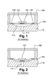
- FIGS. 1 and 2 illustrate a method of manufacturing a concave sensor imager according to the state of the art and described for example in the document US 7,390,687 .
- a planar sensor 100 is firstly produced on the surface of a substrate 102 in which a reading circuit 104 of said sensor 100 and connections 106 are also made, all of which is encapsulated in a box 108. subsequently able to receive an optical (not shown).
- the planar sensor 100 and the substrate 102 are thinned to provide the necessary flexibility to be bent.
- This assembly is then transferred to a second substrate 110 in which is formed a concave cavity 112, having the desired final shape for the sensor 100.
- a passage 114 is furthermore made from the rear face of the substrate 110 to the cavity 112.
- the cavity 112 is then evacuated. A pressure differential is thus created which induces the collapse of the sensor 100 and the substrate 102 in the cavity 112. These latter thus conform to the cavity 112 and the substrate 102 is secured to the cavity 112 by the presence of a glue film previously deposited in the cavity 112.
- the substrate 102 and the sensor 100 are carried on the substrate 110 while the cavity 112 is already formed. Before being conformed to it, the substrate 102 and the sensor 100 therefore do not rest on anything.
- the substrate 102 and the sensor 100 it is difficult, if not impossible, to modify the substrate 102 and the sensor 100 once these are transferred to the cavity 112.
- the modification of the substrate 102 and the sensor 100 that this modification is mechanical (polishing, bonding, etc %), chemical (vacuum deposition, plasma attack, etc ...), or physical (photolithography), necessarily involves applying pressure on them.
- the substrate 102 and the sensor 100 thus bend over the cavity 112, making their modification difficult using conventional methods.
- a variation of the pressure differential applied to the substrate 102 and the sensor 100 causes them to vibrate, again making any delicate modification.
- the method of the state of the art described above allows no modification of the substrate 102 and the sensor 100 once they are reported on the cavity 112. These must be made definitively before their transfer. In particular, they must be reported while they are flexible because of their reduced thickness. The manufacturing process of the imager is therefore strongly constrained.
- the flexibility of the electronic circuits made of silicon is usually obtained when their thickness is less than 50 micrometers. At such thicknesses, their gripping is delicate and any handling error can induce undesired creases or twists.
- the substrate 102 and the sensor 100 are fixed to the casing 108 to facilitate their handling and thus to improve their ease of handling, a casing which prevents a subsequent modification of the casing. imager once the substrate 102 and the sensor 100 conformed to the cavity 112.
- the object of the present invention is to solve the aforementioned problems by proposing an alternative method of producing a non-planar, and in particular concave, microelectronic component using a recess configured accordingly, and by implementing the application of a differential pressure, which substantially reduces the constraints imposed by the realization of the concavity and allows easy handling thereof at any time of its manufacture.
- the subject of the invention is a method for manufacturing a non-planar, and in particular concave, microelectronic component, comprising the superposition of a layer incorporating a flexible active circuit over a cavity shaped according to the profile. that it is desired to impart to said component, formed in a substrate and the application of a pressure differential on either side of said layer, inducing the collapse of the flexible circuit in the cavity, and therefore its conformation with that -this.
- the substrate receiving it has substantially the same mechanical properties as a solid substrate.
- all the constraints related to the cavity before the attack of the material filling the cavity disappear.
- Flexible circuit means a circuit capable of deforming without causing alteration of its structure. Typically, this flexibility results from the thickness of the layer which contains it, and as regards silicon, this layer is of a maximum thickness of 50 micrometers.
- the flexible circuit consists of a conventional CMOS circuit, thinned to a thickness between 2 and 50 microns to obtain under atmospheric pressure a curvature of the thinned substrate with an arrow of 10 to 200um.
- passage or passages may also be performed once the flexible circuit is superimposed on the cavity, or the flexible circuit may comprise orifices allowing access to the material filling the cavity.
- the method comprises one or more of the following features.
- the material filling the cavity is resin capable of being removed by an oxygen plasma.
- the heating makes it possible to reinforce the molecular bonding.
- the at least one passage is blocked, taking care to place the cavity under a first pressure, for example under vacuum or under reduced pressure, the pressure differential being achieved by then subjecting the assembly to a second pressure greater than the first pressure. .
- the collapsed flexible circuit is secured to the cavity.
- the bottom of the cavity is covered with a first material, and the surface of the filling material with the cavity of a second material, said first and second materials being able to form a eutectic system.
- the microelectronic component is an image sensor.
- the invention applies to any type of microelectronic component that it is desired to bend.
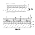
- the process starts ( Figures 3A and 3B ) by forming a thick silicon substrate 12 on which is deposited an SiO 2 layer 14 having a thickness of between 0.05 and 1 micrometer.
- the layer 14 will subsequently serve as a stop layer during the thinning of the substrate 12, as will be explained in more detail later.
- a silicon detection circuit 16 having a thickness of 2 to 5 micrometers, is formed on the layer 14 and comprises detection unit elements 18 (phototransistors or photodiodes for example), or "pixels", as well as electronic components. analog and logic processing of the imager. It therefore constitutes the active circuit in the sense of the invention.
- metal interconnections 22 for the reading and the polarization of the components of the circuit 16, these interconnections are surrounded by dielectric such as SiO forming a layer 20, a thickness of 1.5 to 4 micrometers.
- an SiO 24 silicon oxide layer having a thickness of between 1 and 5 microns is deposited on the dielectric layer 20 comprising the interconnections.
- the layer 24 is then planarized, for example by means of a chemical-mechanical polishing, to allow a subsequent molecular bonding with another substrate, called “handle substrate”, as will be explained in more detail later.
- the detection circuit 16 is a rectangular circuit, the dimensions of which are between 1 and 5 millimeters, and which comprises an array of pixels of 1 to 10 micrometers per side for a total number of pixels of between 300 000 and 12. 000 000.
- the detection circuit 16 and the dielectric layer 20 comprising the interconnections are conventional and define the functional layers of the image sensor of the imager. It will be noted here that all types of sensors and technologies (CMOS, CCD) can be realized here, the choice of these being a function of the intended application. Therefore, the detection circuit 16 and the dielectric layer 20 including the interconnections will not be explained in more detail later. Note simply that the thickness of the elements 16 and 20 makes them flexible.
- the method also comprises the formation of a so-called "handle" silicon substrate 30 on which the deposition of a resin layer 32 having a thickness of, for example, between 10 and 100 micrometers ( figure 4 ).
- a concave cavity 34 is then formed in the resin 32 by means of a convex mold whose shape is the "negative" of the desired shape for the detection circuit 16 ( figure 5 ).
- the thickness of the resin layer 32 is chosen so that the residual thickness e thereof once the cavity formed is as thin as possible, for example of the order of 1 micrometer.
- Ion etching is then performed on the resin layer 32 with a resin / silicon selectivity substantially equal to 1.
- the shape of the cavity 34 printed in the resin layer 32 is thus transferred into the silicon layer 30 to produce a concave cavity 36 in layer 30 ( figure 6 ). If the selectivity of the etching is equal to 1, the cavity 34 is exactly transferred into the layer 30.
- the shape of the cavity 34 is transferred with an amplification factor by choosing a selectivity of less than 1 or with a factor in such a variant where a selectivity other than 1 is chosen, the shape of the mold forming the cavity 34 in the resin layer 32 and the thickness of this layer are adapted so as to obtaining in the silicon layer 30 the desired final shape for the detection circuit 16.
- the residual resin is then removed from the layer 30 and a thermal oxidation of the layer 30 is carried out on a thickness 38 of between 50 nanometers and 0.5 micrometer, for example in an oxidation furnace.
- a metal layer 40 of a thickness between 100 nanometers and 1 micrometer, is then deposited in the cavity 36 ( figure 7 ).
- the metal is for example deposited on the entire surface of the layer 38 and the metal deposited out of the cavity 36 is removed appropriately, for example by means of a masking followed by a selective chemical attack with respect to the oxide of silicon 38 or by mechanochemical polishing.
- the metal of the layer 40 is one of the components of a eutectic system that will allow the subsequent welding of the layer 24 with the bottom of a concave cavity, as will be explained in more detail later.
- the metals forming the eutectic system are chosen so that the melting temperature of this system is less than the melting point of the fragile materials of the imager, in particular the metal of the interconnections of the layer 20 or the subsequently formed microlens material.
- the metal of layer 40 is tin to be combined with gold to form the eutectic system whose melting point is less than 240 ° C.
- the process then continues ( figure 8 ) by depositing a polyimide resin 42 so as to fill the cavity 36 followed by removal of the resin deposited from the cavity 36 to leave the layer 38 of silicon oxide free on the flat portion of the layer 30.
- the assembly is then annealed at a temperature at least equal to the maximum temperature that will undergo said assembly in the following process according to the invention so as to degasify preventively the resin 42 contained in the cavity 36.
- the constituent metal of the layer 26 is, for the eutectic system considered, complementary to the constituent metal of the metal layer 40.
- the metal layer 40 consists of gold.
- the gold / tin eutectic system obtained has a melting point of between 200 ° C. and 240 ° C. depending on the relative proportions of these two metals.
- a dielectric layer 37 for example made of SiO, with a thickness of between 0.1 and 2 micrometers, is then deposited at a temperature below the preceding annealing temperature in order to seal cavity 36.
- the assembly forming the handle substrate 30 is then planarized for example by means of a mechanochemical polishing.
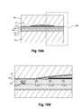
- the assembly comprising the detection circuit 16 and the assembly forming the handle substrate 30 are then transferred to one another so as to match the layers 24 and 37 of silicon oxide ( Figures 10A and 10B ).
- a low temperature molecular bonding of these layers is then performed to secure the two sets, and this bonding is reinforced by heating the whole to a temperature below the annealing temperature of the resin 42.
- a single layer 44 of silicon oxide is thus obtained.
- the substrate 12 arranged under the detection circuit 16 is then thinned ( figure 11 ) so as to be able to detect electromagnetic radiation by the rear face 46 of the imager, the layer 14 made of SiO 2 serving as a stop layer for thinning the substrate 12.
- the substrate 12 is entirely removed.
- the detection circuit 16 with a thickness of between 1 and 5 micrometers then captures the photons as is known per se from the state of the art of rear-illuminated imagers.
- the assembly is then returned ( figure 12 ).
- the process then continues by finalizing the imager according to the intended application.
- the method continues by depositing by photoetching colored resins pellets in red 48, green 50 and blue 52 in relation to the pixels of the detection circuit 16, to define an RGB detection matrix, as is known per se from the field of color detection.
- Microlenses 54 made of transparent resin are then produced on the resin pellets 48, 50, 52 in order to focus the electromagnetic radiation on the unitary detection elements 18 ( figure 3B ) of circuit 16 ( figure 13 ).
- the microlenses 54 are then hardened by annealing carried out at a temperature of between 200 ° C. and 240 ° C.
- microlenses 54 are then protected by the deposition of an uncured resin 56 over the entire surface 46 ( figure 14 ), followed by removal of said resin from the area of microlenses 54, to clear surfaces in which wells will be formed, as explained below.
- a low temperature deposition, below 150 ° C, of a silicon oxide is then carried out to protect the resin deposited on the microlenses 54. It will be noted here that it is the full nature of the handle substrate 30, the cavity 36 being filled, which allows the use of conventional thinning techniques of the substrate 12, photolithography of the resin pellets 48, 50, 52 or embodiment of the microlenses 54.
- emptying wells 58 are formed by photogravure through the layer 14 of the circuit 16, the layer 20 and the layer 44 to reach the cavity 36, and more particularly the resin 42 filling it.
- the wells 58 are formed at the periphery of the pixels of the circuit 16 and have a diameter chosen for subsequent refilling without difficulty.
- the diameter of the wells 58 is between 400 nanometers and 2 micrometers.
- a selective attack of the resin 42 is carried out, in particular using an oxygen plasma brought to said resin by the wells 58.
- This oxygen plasma is known to interact with organic compounds such as resin or polyimide by creating volatile compounds that escape through the wells 58.
- the resin 42 filling the cavity 36 is then completely removed from it ( figure 16 ).
- the process is then continued by evacuation of the assembly and vacuum deposition of a silicon oxide 60 so as to plug the wells 58 ( Figures 17A and 17B ).
- the vacuum to which the assembly was subjected is broken, for example by a return to atmospheric pressure. This then causes the collapse of the layers arranged above the cavity 36 and their conformation with the cavity 36, in particular that of the detection circuit 16 ( Figures 18A and 18B ), because of the pressure differential between the vacuum prevailing within the cavity 36 then emptied of the resin 42, and the atmospheric pressure exerted on the surface 46.
- the process is then continued by removing the protections deposited on the microlenses 54 (SiO 2 layer and resin) using a photolithography.
- the resin is selectively removed from the microlenses 54 because the microlenses were annealed, and thus cured, at a temperature of at least 200 ° C while the protective resin was annealed at a temperature of 150 ° C. ( figure 19 ).
- the assembly is then brought to the melting temperature of the eutectic gold / tin system formed by the layers 26 and 40, so that the oxide layer 24, and consequently all the layers formed above it, are joined together with the bottom of the cavity.
- the handle substrate has a plurality of cavities, preferably circular to best approximate the desired spherical concave shape for the image sensors, formed in the manner previously described, as illustrated in FIG. figure 20 .
- the detection circuits and their associated connections can be made in the same element, as illustrated in FIG. figure 21 .
- FIG. 22 illustrates an alternative embodiment of the cavity 36.
- a hard mask 70 having a thickness of between 100 nanometers and 1 micrometer is formed on the surface of the substrate 30 (FIG. figure 22 ).
- the hardness of the mask 70 is here defined with respect to a subsequent polishing which will not attack, or little, said mask.
- a photoetching of the mask 70 is then performed where the cavity will be formed in the substrate 30 ( figure 23 ), then a mechanochemical polishing is carried out.
- This type of polishing naturally produces a concave surface close to the desired shape for the cavity when it is applied over a large surface ( figure 24 ).
- the present invention has just been described in the context of the manufacture of an imager provided with a concave sensor. Obviously, the present invention is applicable to any type of electronic component requiring a concave surface.
- the cavity 36 is flat and inclined at a predetermined angle with respect to the plane of the handle substrate, so that a plane circuit is obtained which is inclined with respect to the substrate. Micromirrors inclined relative to a reference surface can thus be obtained.
Landscapes
- Physics & Mathematics (AREA)
- Engineering & Computer Science (AREA)
- Power Engineering (AREA)
- Electromagnetism (AREA)
- Condensed Matter Physics & Semiconductors (AREA)
- General Physics & Mathematics (AREA)
- Computer Hardware Design (AREA)
- Microelectronics & Electronic Packaging (AREA)
- Solid State Image Pick-Up Elements (AREA)
- Transforming Light Signals Into Electric Signals (AREA)
- Structure Of Printed Boards (AREA)
Abstract
Description
La présente invention a trait à la réalisation de composants microélectroniques courbés concaves. Elle trouve particulièrement application dans le domaine des capteurs d'images.The present invention relates to the production of concave curved microelectronic components. It finds particular application in the field of image sensors.
Les imageurs électroniques comprennent usuellement un capteur d'image plan semiconducteur réalisé en silicium selon la technologie CMOS ou CCD, et une optique qui forme une image de la scène observée sur le capteur d'image.Electronic imagers usually include a semiconductor planar image sensor made of silicon according to CMOS or CCD technology, and an optic that forms an image of the scene observed on the image sensor.
Toutefois, l'utilisation d'une simple lentille convergente en tant qu'optique n'est pas satisfaisante dans la mesure où l'image formée par une telle lentille n'est pas plane mais sphérique, phénomène connu sous le nom de « courbure de champ ». De fait, l'image projetée par une lentille convergente sur un capteur plan est soit nette au centre mais pas sur les bords soit l'inverse. Ceci explique notamment la fabrication d'optiques complexes, formées de groupes de lentilles, ayant en outre subi des traitements de surface spécifiques afin de conformer les images qu'elles produisent au caractère plan du capteur.However, the use of a simple convergent lens as an optic is not satisfactory insofar as the image formed by such a lens is not flat but spherical, a phenomenon known as the "curvature of field ". In fact, the image projected by a lens convergent on a flat sensor is either sharp in the center but not on the edges or the opposite. This explains in particular the production of complex optics, formed of groups of lenses, having furthermore undergone specific surface treatments in order to conform the images they produce to the flatness of the sensor.
Cependant, même à l'heure actuelle, les optiques les plus complexes introduisent toujours un certain nombre d'aberrations, tant géométriques que chromatiques, au rang desquelles figurent les distorsions en barillet et en coussinet, les aberrations sphériques (ou aberrations dites de « lumière diffuse »), le coma, l'astigmatisme, le vignettage, les éblouissements, la lumière parasite (reflet), ou encore les franges chromatiques.However, even today, the most complex optics always introduce a number of aberrations, both geometrical and chromatic, among which are distortions in barrel and pincushion, spherical aberrations (or aberrations called "light"). diffuse "), coma, astigmatism, vignetting, dazzling, stray light (reflection), or chromatic fringes.
De telles aberrations nécessitent d'être corrigées, directement lors de la formation des images par l'utilisation d'optiques complexes et encombrantes, et/ou a posteriori par la mise en oeuvre d'algorithmes de traitements d'image nécessitant d'importantes puissances de calcul. Ainsi, la nature plane des capteurs induit directement des aberrations et la correction de celles-ci implique des objectifs encombrants et coûteux ainsi que des calculateurs puissants embarqués dans les caméras et les appareils photographiques numériques.Such aberrations need to be corrected, directly during the formation of images by the use of complex and cumbersome optics, and / or a posteriori by the implementation of image processing algorithms requiring large powers. Calculation. Thus, the flat nature of the sensors directly induces aberrations and the correction thereof involves bulky and expensive lenses as well as powerful computers embedded in cameras and digital cameras.
Une manière efficace de faire disparaître les erreurs induites par la courbure de champ est de modifier la forme du capteur d'image de façon à ce qu'il soit sensiblement de même forme que l'image formée par l'optique. Le fait de pouvoir courber le capteur permet donc, non seulement de corriger les aberrations, mais également de concevoir des caméras et des appareils photographiques compacts et bon marché et ne nécessitant pas de grandes puissances de calcul.An effective way of removing the errors induced by the field curvature is to change the shape of the image sensor so that it is substantially of the same shape as the image formed by the optics. Being able to bend the sensor thus makes it possible, not only to correct the aberrations, but also to design compact cameras and cameras that are cheap and do not require high computing power.
On conçoit donc aisément l'intérêt de concevoir des capteurs courbés dans le domaine de la formation d'image.It is therefore easy to understand the interest of designing curved sensors in the field of image formation.
Les
Selon ce procédé, un capteur plan 100 est tout d'abord réalisé à la surface d'un substrat 102 dans lequel sont par ailleurs réalisés un circuit de lecture 104 dudit capteur 100 ainsi que des connexions 106, le tout étant encapsulé dans un boitier 108 apte ultérieurement à recevoir une optique (non représentée). Le capteur plan 100 et le substrat 102 sont amincis pour présenter la souplesse nécessaire afin d'être courbés.According to this method, a
Cet ensemble est ensuite reporté sur un deuxième substrat 110 dans lequel est formée une cavité concave 112, présentant la forme finale recherchée pour le capteur 100. Un passage 114 est par ailleurs réalisé depuis la face arrière du substrat 110 jusqu'à la cavité 112. This assembly is then transferred to a
La cavité 112 est alors mise sous vide. Il se crée ainsi un différentiel de pression qui induit l'affaissement du capteur 100 et du substrat 102 dans la cavité 112. Ces derniers se conforment ainsi à la cavité 112 et le substrat 102 est solidarisé à la cavité 112 par la présence d'un film de colle préalablement déposé dans la cavité 112. The
Toutefois, le substrat 102 et le capteur 100 sont reportés sur le substrat 110 alors que la cavité 112 est déjà formée. Avant d'être conformé à celle-ci, le substrat 102 et le capteur 100 ne reposent donc sur rien.However, the
De fait, il est difficile, voire impossible, de modifier le substrat 102 et le capteur 100 une fois ceux-ci reportés sur la cavité 112. Par exemple il est difficile d'ajouter au substrat 102 ou au capteur 100 de nouveaux éléments tels qu'une couche de protection ou des microlentilles. En effet, la modification du substrat 102 et du capteur 100, que cette modification soit mécanique (polissage, collage, etc...), chimique (dépôt sous vide, attaque par plasma, etc...), ou physique (photolithographie), implique nécessairement d'appliquer une pression sur ceux-ci. Le substrat 102 et le capteur 100 se courbent donc au-dessus de la cavité 112 rendant alors leur modification délicate à l'aide des procédés classiques. Par ailleurs, une variation du différentiel de pression appliqué au substrat 102 et au capteur 100 amène ceux-ci à vibrer, rendant là encore toute modification délicate.In fact, it is difficult, if not impossible, to modify the
Pour pallier ces inconvénients, il convient alors de contrôler très précisément le différentiel de pression auquel ils sont soumis afin de les maintenir plans à tout instant, ce qui s'avère impossible sans une connaissance précise de la pression exercée par les procédés.To overcome these disadvantages, it is then necessary to very precisely control the pressure differential to which they are subjected to maintain planes at any time, which proves impossible without a precise knowledge of the pressure exerted by the processes.
Ainsi, le procédé de l'état de la technique décrit ci-dessus ne permet aucune modification du substrat 102 et du capteur 100 une fois ceux-ci reportés sur la cavité 112. Ces derniers doivent être réalisés de manière définitive avant leur report. Notamment, ils doivent être reportés alors qu'ils sont souples en raison de leur épaisseur réduite. Le processus de fabrication de l'imageur est donc fortement contraint.Thus, the method of the state of the art described above allows no modification of the
De plus, la souplesse des circuits électroniques réalisés en silicium est usuellement obtenue lorsque leur épaisseur est inférieure à 50 micromètres. A de telles épaisseurs, leur préhension est délicate et toute erreur de manipulation peut induire des pliures ou des vrillages non souhaités. D'ailleurs, dans l'exemple de procédé exposé ci-dessus, le substrat 102 et le capteur 100 sont fixés au boîtier 108 pour faciliter leur manipulation et ainsi gagner en facilité de manipulation, boîtier qui fait obstacle à une modification ultérieure de l'imageur une fois le substrat 102 et le capteur 100 conformés à la cavité 112. In addition, the flexibility of the electronic circuits made of silicon is usually obtained when their thickness is less than 50 micrometers. At such thicknesses, their gripping is delicate and any handling error can induce undesired creases or twists. Moreover, in the example of the process described above, the
Le but de la présente invention est de résoudre les problèmes susmentionnés en proposant un procédé alternatif de réalisation d'un composant microélectronique non plan, et notamment concave, à l'aide d'une cavité conformée en conséquence, et par la mise en oeuvre de l'application d'un différentiel de pression, qui diminue sensiblement les contraintes imposées par la réalisation de la concavité et autorise une manipulation aisée de celui-ci à tout instant de sa fabrication.The object of the present invention is to solve the aforementioned problems by proposing an alternative method of producing a non-planar, and in particular concave, microelectronic component using a recess configured accordingly, and by implementing the application of a differential pressure, which substantially reduces the constraints imposed by the realization of the concavity and allows easy handling thereof at any time of its manufacture.
A cet effet, l'invention a pour objet un procédé de fabrication d'un composant microélectronique non plan, et notamment concave, comprenant la superposition d'une couche intégrant un circuit actif souple au-dessus d'une cavité conformée selon le profil que l'on souhaite conférer audit composant, formée dans un substrat et l'application d'un différentiel de pression de part et d'autre de ladite couche, induisant l'affaissement du circuit souple dans la cavité, et donc sa conformation avec celle-ci.For this purpose, the subject of the invention is a method for manufacturing a non-planar, and in particular concave, microelectronic component, comprising the superposition of a layer incorporating a flexible active circuit over a cavity shaped according to the profile. that it is desired to impart to said component, formed in a substrate and the application of a pressure differential on either side of said layer, inducing the collapse of the flexible circuit in the cavity, and therefore its conformation with that -this.
Selon l'invention, la superposition du circuit souple et de la cavité est réalisée :
- ■ par remplissage préalable de la cavité par un matériau apte à être enlevé sélectivement par rapport au substrat et au circuit souple ;
- ■ puis, par report ou formation du circuit souple sur la cavité ainsi remplie ;
- ■ puis, par formation d'au moins un passage d'accès à la cavité remplie ; et
- ■ par attaque sélective du matériau remplissant la cavité via le au moins passage d'accès afin d'ôter ledit matériau.
- ■ by prior filling of the cavity with a material capable of being removed selectively with respect to the substrate and the flexible circuit;
- ■ then, by postponement or formation of the flexible circuit on the thus filled cavity;
- ■ then, by forming at least one access passage to the filled cavity; and
- By selective etching of the material filling the cavity via the at least access passage in order to remove said material.
En d'autres termes, une fois la cavité remplie, le substrat recevant celle-ci présente sensiblement les mêmes propriétés mécaniques qu'un substrat plein. De fait, toutes les contraintes liées à la cavité avant l'attaque du matériau remplissant la cavité disparaissent. Notamment, il est possible, au choix, de réaliser directement le circuit souple sur le substrat à l'aide de procédés classiques, de reporter le circuit souple une fois celui-ci fabriqué ou encore de reporter un bloc épais comprenant le circuit souple puis d'amincir celui-ci par des procédés classiques. Il est encore possible de modifier le circuit souple une fois celui-ci superposé au substrat car il repose sur une surface pleine.In other words, once the cavity is filled, the substrate receiving it has substantially the same mechanical properties as a solid substrate. In fact, all the constraints related to the cavity before the attack of the material filling the cavity disappear. In particular, it is possible, as desired, to directly produce the flexible circuit on the substrate using conventional methods, to postpone the flexible circuit once it is manufactured or to postpone a thick block comprising the flexible circuit and then d to thin it by conventional methods. It is still possible to modify the flexible circuit once it superimposed on the substrate because it rests on a solid surface.
Par circuit « souple », on entend un circuit susceptible de se déformer sans engendrer d'altération de sa structure. Typiquement, cette souplesse résulte de l'épaisseur de la couche qui le contient, et s'agissant du silicium, cette couche est d'une épaisseur maximum de 50 micromètres."Flexible" circuit means a circuit capable of deforming without causing alteration of its structure. Typically, this flexibility results from the thickness of the layer which contains it, and as regards silicon, this layer is of a maximum thickness of 50 micrometers.
Par « concave », on entend ici un volume ménagé en creux.By "concave" is meant here a hollow volume.
Par exemple, le circuit souple est constitué d'un circuit CMOS classique, aminci à une épaisseur comprise entre 2 et 50 microns permettant d'obtenir sous pression atmosphérique une courbure du substrat aminci avec une flèche de 10 à 200um.For example, the flexible circuit consists of a conventional CMOS circuit, thinned to a thickness between 2 and 50 microns to obtain under atmospheric pressure a curvature of the thinned substrate with an arrow of 10 to 200um.
La formation du ou des passages peut par ailleurs être réalisée une fois le circuit souple superposé sur la cavité, ou bien le circuit souple peut comporter des orifices permettant l'accès au matériau remplissant la cavité.The formation of the passage or passages may also be performed once the flexible circuit is superimposed on the cavity, or the flexible circuit may comprise orifices allowing access to the material filling the cavity.
Selon des modes de réalisation particuliers de l'invention, le procédé comporte une ou plusieurs des caractéristiques suivantes.According to particular embodiments of the invention, the method comprises one or more of the following features.
Le matériau remplissant la cavité est de la résine apte à être enlevée par un plasma d'oxygène.The material filling the cavity is resin capable of being removed by an oxygen plasma.
Le circuit souple est collé sur le substrat par collage moléculaire. Notamment :
- ■ le circuit souple est recouvert d'une couche d'oxyde de silicium;
- ■ le substrat est recouvert d'une couche d'oxyde de silicium une fois la cavité formée et remplie ;
- ■ le circuit souple est reporté sur le substrat, avec la couche d'oxyde de silicium du circuit souple déposée sur la couche d'oxyde de silicium du substrat ;
- ■ et un chauffage des couches d'oxyde de silicium est réalisé.
- The flexible circuit is covered with a layer of silicon oxide;
- The substrate is covered with a layer of silicon oxide once the cavity has been formed and filled;
- The flexible circuit is carried on the substrate, with the silicon oxide layer of the flexible circuit deposited on the silicon oxide layer of the substrate;
- And heating of the silicon oxide layers is performed.
Le chauffage permet notamment de renforcer le collage moléculaire.The heating makes it possible to reinforce the molecular bonding.
Le au moins un passage est bouché en prenant soin de placer la cavité sous une première pression, et par exemple sous vide ou sous pression réduite, le différentiel de pression étant réalisé en soumettant ensuite l'ensemble à une seconde pression supérieure à la première pression.The at least one passage is blocked, taking care to place the cavity under a first pressure, for example under vacuum or under reduced pressure, the pressure differential being achieved by then subjecting the assembly to a second pressure greater than the first pressure. .
Selon un mode particulier de réalisation de l'invention, le circuit souple affaissé est solidarisé avec la cavité. Notamment, on recouvre le fond de la cavité d'un premier matériau, et la surface du matériau de remplissage de la cavité d'un second matériau, lesdits premier et second matériaux étant aptes à former un système eutectique. Une fois le matériau de remplissage de la cavité ôté, le circuit souple est solidarisé à la cavité en portant le composant à la température eutectique du système eutectique.According to a particular embodiment of the invention, the collapsed flexible circuit is secured to the cavity. In particular, the bottom of the cavity is covered with a first material, and the surface of the filling material with the cavity of a second material, said first and second materials being able to form a eutectic system. Once the filling material of the cavity has been removed, the flexible circuit is secured to the cavity by bringing the component to the eutectic temperature of the eutectic system.
Le composant microélectronique est un capteur d'image. L'invention s'applique toutefois à tout type de composant microélectronique que l'on souhaite courber.The microelectronic component is an image sensor. The invention, however, applies to any type of microelectronic component that it is desired to bend.
L'invention sera mieux comprise à la lecture de la description qui suit, donnée uniquement à titre d'exemple, et réalisée en relation avec les dessins annexés, dans lesquels des références identiques désignent des éléments identiques ou fonctionnellement analogues, et dans lesquels :
- ■ les
figures 1 et 2 sont des vues schématiques en section d'un imageur électronique à illumination par la face arrière lors de sa fabrication selon un procédé de l'état de la technique ; - ■ les
figures 3 à 19 sont des vues en section d'un imageur électronique lors de différentes étapes de fabrication selon le procédé selon l'invention ; - ■ les
figures 20 et 21 sont respectivement des vues de dessus d'un substrat dans lequel sont formées plusieurs cavités et d'une galette comportant une pluralité de capteurs d'image pour une fabrication simultanée de plusieurs imageurs concaves ; et - ■ les
figures 22 à 24 sont des vues en section d'un substrat dit de poignée lors d'une variante de réalisation d'une cavité concave.
- ■ the
Figures 1 and 2 are diagrammatic cross-sectional views of an electronic imager with back-side illumination during its manufacture according to a method of the state of the art; - ■ the
Figures 3 to 19 are sectional views of an electronic imager during different manufacturing steps according to the method according to the invention; - ■ the
Figures 20 and 21 are respectively top views of a substrate in which are formed several cavities and a wafer having a plurality of image sensors for simultaneous manufacture of several concave imagers; and - ■ the
Figures 22 to 24 are views in section of a so-called handle substrate in a variant embodiment of a concave cavity.
Il va à présent être décrit un procédé de fabrication d'un imageur électronique à illumination par la face arrière (ou imageur « back side » selon l'expression anglo-saxonne), dont le capteur d'image est concave.It will now be described a method of manufacturing an electronic imager with illumination by the back side (or imager " back side " according to the English expression), whose image sensor is concave.
Le procédé débute (
Un circuit de détection en silicium 16, d'une épaisseur de 2 à 5 micromètres, est formé sur la couche 14 et comporte des éléments unitaires de détection 18 (phototransistors ou photodiodes par exemple), ou « pixels », ainsi que des composants électroniques de traitement analogique et logique de l'imageur. Il constitue donc le circuit actif au sens de l'invention.A
Sur le circuit 16 sont réalisées des interconnexions métalliques 22 pour la lecture et la polarisation des composants du circuit 16, ces interconnexions sont environnées de diélectrique tel que le SiO formant une couche 20, d'une épaisseur de 1,5 à 4 micromètres..On the
Enfin, une couche d'oxyde de silicium SiO 24, d'une épaisseur comprise entre 1 et 5 micromètres, est déposée sur la couche de diélectrique 20 comprenant les interconnexions. La couche 24 est ensuite planarisée, par exemple au moyen d'un polissage mécano-chimique, afin de permettre un collage moléculaire ultérieur avec un autre substrat, dit « substrat poignée », comme cela sera expliqué plus en détail par la suite.Finally, an
Par exemple, le circuit de détection 16 est un circuit rectangulaire, dont les dimensions sont comprises entre 1 et 5 millimètres, et qui comporte un réseau de pixels de 1 à 10 micromètres de côté pour un nombre total de pixels compris entre 300 000 et 12 000 000.For example, the
On retiendra que le circuit de détection 16 et la couche de diélectrique 20 comprenant les interconnexions sont classiques et définissent les couches fonctionnelles du capteur d'image de l'imageur. On notera ici que tout type de capteurs et de technologies (CMOS, CCD) peut être ici réalisé, le choix de ceux-ci étant fonction de l'application visée. Par conséquent, le circuit de détection 16 et la couche de diélectrique 20 comprenant les interconnexions ne seront pas expliqués plus en détail par la suite. On notera simplement que l'épaisseur des éléments 16 et 20 rend ceux-ci souples.It will be noted that the
Le procédé comporte par ailleurs la formation d'un substrat en silicium dit « de poignée » 30 sur lequel est réalisé le dépôt d'une couche de résine 32 d'une épaisseur par exemple comprise entre 10 et 100 micromètres (
Une cavité concave 34 est alors formée dans la résine 32 à l'aide d'un moule convexe dont la forme est le « négatif » de la forme souhaitée pour le circuit de détection 16 (
Une gravure ionique est alors réalisée sur la couche de résine 32 avec une sélectivité résine/silicium sensiblement égale à 1. La forme de la cavité 34 imprimée dans la couche de résine 32 est ainsi transférée dans la couche de silicium 30 pour réaliser une cavité concave 36 dans la couche 30 (
La résine résiduelle est alors retirée de la couche 30 et une oxydation thermique de la couche 30 est réalisée sur une épaisseur 38 comprise entre 50 nanomètres et 0,5 micromètre, par exemple dans un four d'oxydation.The residual resin is then removed from the
Une couche de métal 40, d'une épaisseur comprise entre 100 nanomètres et 1 micromètre, est ensuite déposée dans la cavité 36 (
Le métal de la couche 40 constitue l'un des composants d'un système eutectique qui permettra la soudure ultérieure de la couche 24 avec le fond d'une cavité concave, comme cela sera expliqué plus en détail par la suite. Les métaux formant le système eutectique sont choisis pour que la température de fusion de ce système soit inférieure à la température de fusion des matériaux fragiles de l'imageur, notamment le métal des interconnexions de la couche 20 ou encore le matériau de microlentilles ultérieurement formées. Par exemple, le métal de la couche 40 est de l'étain destiné à être combiné avec de l'or pour former le système eutectique dont la température de fusion est inférieure à 240°C.The metal of the
Le procédé se poursuit alors (
L'ensemble est alors recuit à une température au moins égale à la température maximale que subira ledit ensemble dans la suite du procédé selon l'invention de manière à dégazer préventivement la résine 42 contenue dans la cavité 36. The assembly is then annealed at a temperature at least equal to the maximum temperature that will undergo said assembly in the following process according to the invention so as to degasify preventively the
Une couche de métal 26, d'une épaisseur comprise entre 100 nanomètres et 1 micromètre, est déposée sur la résine de remplissage 42 (
Une couche de diélectrique 37, par exemple en SiO, d'épaisseur comprise entre 0,1 et 2 micromètres est alors déposée à une température inférieure à la température de recuit précédente pour réaliser le scellement de la cavité 36. A
L'ensemble formant le substrat poignée 30 est alors planarisé par exemple au moyen d'un polissage mécanochimique.The assembly forming the
L'ensemble comportant le circuit de détection 16 et l'ensemble formant le substrat poignée 30 sont alors reportés l'un sur l'autre de manière à mettre en correspondance les couches 24 et 37 d'oxyde de silicium (
Un collage moléculaire à basse température de ces couches est alors réalisé pour solidariser les deux ensembles, puis ce collage est renforcé en chauffant le tout à une température inférieure à la température de recuit de la résine 42. Une seule couche 44 d'oxyde de silicium est ainsi obtenue.A low temperature molecular bonding of these layers is then performed to secure the two sets, and this bonding is reinforced by heating the whole to a temperature below the annealing temperature of the
Le substrat 12 agencé sous le circuit de détection 16 est ensuite aminci (
Dans le mode de réalisation présenté, le substrat 12 est entièrement retiré. Le circuit de détection 16 d'épaisseur comprise entre 1 et 5 micromètres réalise alors la capture des photons comme cela est connu en soi de l'état de la technique des imageurs à illumination par la face arrière.In the embodiment shown, the
Une fois l'amincissement du substrat 12 réalisé, l'ensemble est alors retourné (
Le procédé se poursuit alors par la finalisation de l'imageur en fonction de l'application visée.The process then continues by finalizing the imager according to the intended application.
Par exemple, si une détection dans le domaine visible est visée, le procédé se poursuit par le dépôt par photogravure de pastilles de résines colorées en rouge 48, en vert 50 et en bleu 52 en regard des pixels du circuit de détection 16, afin de définir un matriçage de détection RVB, comme cela est connu en soi du domaine de la détection en couleurs. Des microlentilles 54 en résine transparente sont ensuite réalisées sur les pastilles de résines 48, 50, 52 afin de focaliser le rayonnement électromagnétique sur les éléments de détection unitaire 18 (
Les microlentilles 54 sont alors protégées par le dépôt d'une résine non durcie 56 sur toute la surface 46 (
Une fois la partie détection et optique 57 de l'imageur finalisées, le procédé se poursuit par la courbure de cette partie 57. Once the detection and
Plus particulièrement, des puits de vidage 58 sont formés par photogravure au travers de la couche 14 du circuit 16, de la couche 20 et de la couche 44 pour atteindre la cavité 36, et plus particulièrement la résine 42 remplissant celle-ci. Les puits 58 sont formés en périphérie des pixels du circuit 16 et présentent un diamètre choisi pour un rebouchage ultérieur sans difficulté. Par exemple le diamètre des puits 58 est compris entre 400 nanomètres et 2 micromètres.More particularly, emptying
Une fois les puits 58 formés, une attaque sélective de la résine 42 est réalisée, notamment à l'aide d'un plasma d'oxygène amené jusqu'à ladite résine par les puits 58. Ce plasma d'oxygène est connu pour interagir avec les composés organiques tels que la résine ou le polyimide en créant des composés volatils qui s'échappent par les puits 58. La résine 42 remplissant la cavité 36 est alors entièrement retirée de celle-ci (
Une fois la cavité 36 vidée, celle-ci est à une pression identique à la pression extérieure grâce aux puits 58. Il n'existe donc à ce stade aucun différentiel de pression entre la cavité et l'environnement, quelle que soit la pression de ce dernier.Once the
Le procédé se poursuit alors par la mise sous vide de l'ensemble et du dépôt sous vide d'un oxyde de silicium 60 de manière à boucher les puits 58 (
Une fois les puits 58 rebouchés, le vide auquel était soumis l'ensemble est cassé, par exemple par une remise à la pression atmosphérique. Ceci provoque alors l'affaissement des couches agencées au dessus de la cavité 36 et leur conformation à la cavité 36, notamment celle du circuit de détection 16 (
Le procédé se poursuit alors par le retrait des protections déposées sur les microlentilles 54 (couche de SiO2 et résine) à l'aide d'une photolithographie. La résine est retirée sélectivement des microlentilles 54 car ces dernières ont été recuites, et donc durcies, à une température d'au moins 200°C alors que la résine de protection a subi un recuit d'une température de 150°C. (
L'ensemble est alors porté à la température de fusion du système eutectique or/étain formé des couches 26 et 40, de sorte que la couche d'oxyde 24, et par suite toutes les couches formées au dessus de celle-ci, sont solidarisées avec le fond de la cavité.The assembly is then brought to the melting temperature of the eutectic gold / tin system formed by the
Il a été décrit la formation d'un capteur concave. Une pluralité de capteurs concaves peut cependant être réalisée simultanément. Par exemple, le substrat poignée comporte une pluralité de cavités, de préférence circulaires pour s'approcher au mieux de la forme concave sphérique recherchée pour les capteurs d'image, formées de la manière décrite précédemment, comme cela est illustré à la
Les
Une photogravure du masque 70 est ensuite réalisée à l'endroit où la cavité sera formée dans le substrat 30 (
La présente invention vient d'être décrite dans le cadre de la fabrication d'un imageur muni d'un capteur concave. On comprendra évidemment que la présente invention trouve application à tout type de composants électroniques nécessitant d'avoir une surface concave. Par exemple, la cavité 36 est plane et inclinée d'un angle prédéterminé par rapport au plan du substrat poignée, de sorte qu'il est obtenu un circuit plan et incliné par rapport au substrat. Des micromiroirs inclinés par rapport à une surface de référence peuvent ainsi être obtenus.The present invention has just been described in the context of the manufacture of an imager provided with a concave sensor. Obviously, the present invention is applicable to any type of electronic component requiring a concave surface. For example, the
Claims (8)
caractérisé en ce que la superposition du circuit souple (16, 20, 24) et de la cavité (36) est réalisée :
characterized in that the superposition of the flexible circuit (16, 20, 24) and the cavity (36) is carried out:
Applications Claiming Priority (1)
| Application Number | Priority Date | Filing Date | Title |
|---|---|---|---|
| FR0959340A FR2954580B1 (en) | 2009-12-22 | 2009-12-22 | METHOD FOR PRODUCING A NON-PLAN MICROELECTRONIC COMPONENT |
Publications (3)
| Publication Number | Publication Date |
|---|---|
| EP2339630A2 true EP2339630A2 (en) | 2011-06-29 |
| EP2339630A3 EP2339630A3 (en) | 2014-04-02 |
| EP2339630B1 EP2339630B1 (en) | 2015-05-27 |
Family
ID=42338329
Family Applications (1)
| Application Number | Title | Priority Date | Filing Date |
|---|---|---|---|
| EP10306169.3A Active EP2339630B1 (en) | 2009-12-22 | 2010-10-26 | Fabrication process of a non-planar microelectronic device |
Country Status (5)
| Country | Link |
|---|---|
| US (1) | US7935559B1 (en) |
| EP (1) | EP2339630B1 (en) |
| JP (1) | JP2011135047A (en) |
| CN (1) | CN102117818A (en) |
| FR (1) | FR2954580B1 (en) |
Cited By (1)
| Publication number | Priority date | Publication date | Assignee | Title |
|---|---|---|---|---|
| FR2989519A1 (en) * | 2012-04-13 | 2013-10-18 | St Microelectronics Crolles 2 | METHOD OF MANUFACTURING A CURVED SURFACE IMAGE SENSOR |
Families Citing this family (19)
| Publication number | Priority date | Publication date | Assignee | Title |
|---|---|---|---|---|
| US8273603B2 (en) * | 2008-04-04 | 2012-09-25 | The Charles Stark Draper Laboratory, Inc. | Interposers, electronic modules, and methods for forming the same |
| US8017451B2 (en) | 2008-04-04 | 2011-09-13 | The Charles Stark Draper Laboratory, Inc. | Electronic modules and methods for forming the same |
| FR2942070B1 (en) * | 2009-02-11 | 2011-03-11 | Commissariat Energie Atomique | METHOD FOR CORRECTING ASTIGMATISM IN IMAGING BY ELECTRON EMISSION SPECTROMICROSCOPY |
| US8621749B2 (en) * | 2010-03-12 | 2014-01-07 | Taiwan Green Point Enterprises Co., Ltd | Non-deleterious technique for creating continuous conductive circuits |
| US8952919B2 (en) | 2011-02-25 | 2015-02-10 | Taiwan Green Point Enterprises Co., Ltd. | Capacitive touch sensitive housing and method for making the same |
| US20120273261A1 (en) | 2010-10-20 | 2012-11-01 | Taiwan Green Point Enterprises Co., Ltd. | Circuit substrate having a circuit pattern and method for making the same |
| JP5724322B2 (en) * | 2010-11-24 | 2015-05-27 | ソニー株式会社 | Method for manufacturing solid-state imaging device |
| FR2976719A1 (en) * | 2011-06-16 | 2012-12-21 | Commissariat Energie Atomique | METHOD FOR PRODUCING A BILAMIC CURVED MICROELECTRONIC COMPONENT, AND MICROELECTRONIC COMPONENT THUS OBTAINED |
| FR2989518A1 (en) | 2012-04-13 | 2013-10-18 | St Microelectronics Crolles 2 | Method for manufacturing integrated image sensor, involves forming pixels at end of columns, and deforming structure such that another end of each of columns is brought closer or separated to form surface in shape of polyhedral cap |
| US8968637B2 (en) | 2012-06-18 | 2015-03-03 | Honeywell Federal Manufacturing & Technologies, Llc | Method and system for fabricating dome shaped LTCC substrates |
| JP6056432B2 (en) * | 2012-12-06 | 2017-01-11 | 三菱マテリアル株式会社 | Power module substrate, power module substrate with heat sink, power module, power module substrate manufacturing method |
| WO2016018288A1 (en) | 2014-07-30 | 2016-02-04 | Hewlett-Packard Development Company, L.P. | Hybrid multilayer device |
| US10658177B2 (en) | 2015-09-03 | 2020-05-19 | Hewlett Packard Enterprise Development Lp | Defect-free heterogeneous substrates |
| US9893058B2 (en) * | 2015-09-17 | 2018-02-13 | Semiconductor Components Industries, Llc | Method of manufacturing a semiconductor device having reduced on-state resistance and structure |
| US10586847B2 (en) * | 2016-01-15 | 2020-03-10 | Hewlett Packard Enterprise Development Lp | Multilayer device |
| WO2017171737A1 (en) | 2016-03-30 | 2017-10-05 | Hewlett Packard Enterprise Development Lp | Devices having substrates with selective airgap regions |
| FR3073322B1 (en) * | 2017-11-07 | 2021-12-03 | Commissariat Energie Atomique | PROCESS FOR MAKING AT LEAST ONE CURVED ELECTRONIC CIRCUIT |
| FR3077159A1 (en) * | 2018-01-22 | 2019-07-26 | Stmicroelectronics (Crolles 2) Sas | IMAGE SENSOR AND METHOD FOR MANUFACTURING SAME |
| US10381801B1 (en) | 2018-04-26 | 2019-08-13 | Hewlett Packard Enterprise Development Lp | Device including structure over airgap |
Citations (1)
| Publication number | Priority date | Publication date | Assignee | Title |
|---|---|---|---|---|
| US7390687B2 (en) | 2005-02-18 | 2008-06-24 | Micron Technology, Inc. | Microelectronic imagers with shaped image sensors and methods for manufacturing microelectronic imagers |
Family Cites Families (4)
| Publication number | Priority date | Publication date | Assignee | Title |
|---|---|---|---|---|
| JP2005260436A (en) * | 2004-03-10 | 2005-09-22 | Mitsubishi Electric Corp | Imaging module and imaging apparatus employing it |
| US7397066B2 (en) * | 2004-08-19 | 2008-07-08 | Micron Technology, Inc. | Microelectronic imagers with curved image sensors and methods for manufacturing microelectronic imagers |
| JP2007266380A (en) * | 2006-03-29 | 2007-10-11 | Matsushita Electric Ind Co Ltd | Semiconductor image pickup device and its manufacturing method |
| KR101378418B1 (en) * | 2007-11-01 | 2014-03-27 | 삼성전자주식회사 | image sensor module and fabrication method thereof |
-
2009
- 2009-12-22 FR FR0959340A patent/FR2954580B1/en not_active Expired - Fee Related
-
2010
- 2010-10-26 EP EP10306169.3A patent/EP2339630B1/en active Active
- 2010-10-27 US US12/913,289 patent/US7935559B1/en active Active
- 2010-10-28 JP JP2010242083A patent/JP2011135047A/en active Pending
- 2010-11-29 CN CN2010105631187A patent/CN102117818A/en active Pending
Patent Citations (1)
| Publication number | Priority date | Publication date | Assignee | Title |
|---|---|---|---|---|
| US7390687B2 (en) | 2005-02-18 | 2008-06-24 | Micron Technology, Inc. | Microelectronic imagers with shaped image sensors and methods for manufacturing microelectronic imagers |
Cited By (1)
| Publication number | Priority date | Publication date | Assignee | Title |
|---|---|---|---|---|
| FR2989519A1 (en) * | 2012-04-13 | 2013-10-18 | St Microelectronics Crolles 2 | METHOD OF MANUFACTURING A CURVED SURFACE IMAGE SENSOR |
Also Published As
| Publication number | Publication date |
|---|---|
| US7935559B1 (en) | 2011-05-03 |
| EP2339630A3 (en) | 2014-04-02 |
| EP2339630B1 (en) | 2015-05-27 |
| FR2954580A1 (en) | 2011-06-24 |
| FR2954580B1 (en) | 2011-12-09 |
| JP2011135047A (en) | 2011-07-07 |
| CN102117818A (en) | 2011-07-06 |
Similar Documents
| Publication | Publication Date | Title |
|---|---|---|
| EP2339630B1 (en) | Fabrication process of a non-planar microelectronic device | |
| EP2279524B1 (en) | Method of producing an optical device consisting of integrated optoelectronic components | |
| EP1243903B1 (en) | Radiation detectors and method of manufacturing the same | |
| EP2335037B1 (en) | Electromagnetic radiation detector with micro-encapsulation, and device for detecting electromagnetic radiation using such detectors | |
| EP3579028B1 (en) | Image sensors comprising a matrix of interferential filters | |
| FR2989518A1 (en) | Method for manufacturing integrated image sensor, involves forming pixels at end of columns, and deforming structure such that another end of each of columns is brought closer or separated to form surface in shape of polyhedral cap | |
| EP2628708B1 (en) | Microelectronic substrate having a buried layer of organic material | |
| EP2339623B1 (en) | method for producing a non-planar element | |
| FR2943177A1 (en) | METHOD FOR MANUFACTURING A MULTILAYER STRUCTURE WITH CIRCUIT LAYER REPORT | |
| FR3073322A1 (en) | METHOD FOR PRODUCING AT LEAST ONE CURVED ELECTRONIC CIRCUIT | |
| EP3399290A1 (en) | Electromagnetic radiation detector, encapsulated by adding a thin layer | |
| FR2969378A1 (en) | THREE-DIMENSIONAL COMPOSITE STRUCTURE HAVING MULTIPLE LAYERS OF ALIGNMENT MICROCOMPONENTS | |
| FR2952473A1 (en) | METHOD FOR PRODUCING A CURVED CIRCUIT | |
| EP2697825B1 (en) | Method for manufacturing an opto-microelectronic device | |
| EP3809467B1 (en) | Method for collective curvature of a set of electronic chips | |
| EP4107579A1 (en) | Optical component with encapsulated metasurface and method for manufacturing such a component | |
| FR3108786A1 (en) | Pixel of a light sensor and its manufacturing process | |
| WO2023156717A1 (en) | Method for producing an elementary detector for an infrared sensor, associated elementary detector and associated infrared sensor | |
| WO2019158833A1 (en) | Removable structure and removal method using said structure | |
| WO2017046287A1 (en) | Lithography mould for nanometric impression and methods for manufacturing and using such a mould | |
| FR3077159A1 (en) | IMAGE SENSOR AND METHOD FOR MANUFACTURING SAME | |
| FR2939962A1 (en) | METHOD OF SLURING A STRUCTURE |
Legal Events
| Date | Code | Title | Description |
|---|---|---|---|
| PUAI | Public reference made under article 153(3) epc to a published international application that has entered the european phase |
Free format text: ORIGINAL CODE: 0009012 |
|
| AK | Designated contracting states |
Kind code of ref document: A2 Designated state(s): AL AT BE BG CH CY CZ DE DK EE ES FI FR GB GR HR HU IE IS IT LI LT LU LV MC MK MT NL NO PL PT RO RS SE SI SK SM TR |
|
| AX | Request for extension of the european patent |
Extension state: BA ME |
|
| PUAL | Search report despatched |
Free format text: ORIGINAL CODE: 0009013 |
|
| AK | Designated contracting states |
Kind code of ref document: A3 Designated state(s): AL AT BE BG CH CY CZ DE DK EE ES FI FR GB GR HR HU IE IS IT LI LT LU LV MC MK MT NL NO PL PT RO RS SE SI SK SM TR |
|
| AX | Request for extension of the european patent |
Extension state: BA ME |
|
| RIC1 | Information provided on ipc code assigned before grant |
Ipc: H01L 27/146 20060101AFI20140225BHEP |
|
| 17P | Request for examination filed |
Effective date: 20140922 |
|
| RBV | Designated contracting states (corrected) |
Designated state(s): AL AT BE BG CH CY CZ DE DK EE ES FI FR GB GR HR HU IE IS IT LI LT LU LV MC MK MT NL NO PL PT RO RS SE SI SK SM TR |
|
| GRAP | Despatch of communication of intention to grant a patent |
Free format text: ORIGINAL CODE: EPIDOSNIGR1 |
|
| INTG | Intention to grant announced |
Effective date: 20150319 |
|
| GRAS | Grant fee paid |
Free format text: ORIGINAL CODE: EPIDOSNIGR3 |
|
| GRAA | (expected) grant |
Free format text: ORIGINAL CODE: 0009210 |
|
| AK | Designated contracting states |
Kind code of ref document: B1 Designated state(s): AL AT BE BG CH CY CZ DE DK EE ES FI FR GB GR HR HU IE IS IT LI LT LU LV MC MK MT NL NO PL PT RO RS SE SI SK SM TR |
|
| REG | Reference to a national code |
Ref country code: GB Ref legal event code: FG4D Free format text: NOT ENGLISH |
|
| REG | Reference to a national code |
Ref country code: CH Ref legal event code: EP |
|
| REG | Reference to a national code |
Ref country code: AT Ref legal event code: REF Ref document number: 729254 Country of ref document: AT Kind code of ref document: T Effective date: 20150615 |
|
| REG | Reference to a national code |
Ref country code: IE Ref legal event code: FG4D Free format text: LANGUAGE OF EP DOCUMENT: FRENCH |
|
| REG | Reference to a national code |
Ref country code: DE Ref legal event code: R096 Ref document number: 602010024883 Country of ref document: DE Effective date: 20150709 |
|
| REG | Reference to a national code |
Ref country code: AT Ref legal event code: MK05 Ref document number: 729254 Country of ref document: AT Kind code of ref document: T Effective date: 20150527 |
|
| REG | Reference to a national code |
Ref country code: LT Ref legal event code: MG4D |
|
| PG25 | Lapsed in a contracting state [announced via postgrant information from national office to epo] |
Ref country code: LT Free format text: LAPSE BECAUSE OF FAILURE TO SUBMIT A TRANSLATION OF THE DESCRIPTION OR TO PAY THE FEE WITHIN THE PRESCRIBED TIME-LIMIT Effective date: 20150527 Ref country code: ES Free format text: LAPSE BECAUSE OF FAILURE TO SUBMIT A TRANSLATION OF THE DESCRIPTION OR TO PAY THE FEE WITHIN THE PRESCRIBED TIME-LIMIT Effective date: 20150527 Ref country code: NO Free format text: LAPSE BECAUSE OF FAILURE TO SUBMIT A TRANSLATION OF THE DESCRIPTION OR TO PAY THE FEE WITHIN THE PRESCRIBED TIME-LIMIT Effective date: 20150827 Ref country code: HR Free format text: LAPSE BECAUSE OF FAILURE TO SUBMIT A TRANSLATION OF THE DESCRIPTION OR TO PAY THE FEE WITHIN THE PRESCRIBED TIME-LIMIT Effective date: 20150527 Ref country code: PT Free format text: LAPSE BECAUSE OF FAILURE TO SUBMIT A TRANSLATION OF THE DESCRIPTION OR TO PAY THE FEE WITHIN THE PRESCRIBED TIME-LIMIT Effective date: 20150928 Ref country code: FI Free format text: LAPSE BECAUSE OF FAILURE TO SUBMIT A TRANSLATION OF THE DESCRIPTION OR TO PAY THE FEE WITHIN THE PRESCRIBED TIME-LIMIT Effective date: 20150527 |
|
| REG | Reference to a national code |
Ref country code: FR Ref legal event code: PLFP Year of fee payment: 6 |
|
| REG | Reference to a national code |
Ref country code: NL Ref legal event code: MP Effective date: 20150527 |
|
| PG25 | Lapsed in a contracting state [announced via postgrant information from national office to epo] |
Ref country code: AT Free format text: LAPSE BECAUSE OF FAILURE TO SUBMIT A TRANSLATION OF THE DESCRIPTION OR TO PAY THE FEE WITHIN THE PRESCRIBED TIME-LIMIT Effective date: 20150527 Ref country code: BG Free format text: LAPSE BECAUSE OF FAILURE TO SUBMIT A TRANSLATION OF THE DESCRIPTION OR TO PAY THE FEE WITHIN THE PRESCRIBED TIME-LIMIT Effective date: 20150827 Ref country code: GR Free format text: LAPSE BECAUSE OF FAILURE TO SUBMIT A TRANSLATION OF THE DESCRIPTION OR TO PAY THE FEE WITHIN THE PRESCRIBED TIME-LIMIT Effective date: 20150828 Ref country code: IS Free format text: LAPSE BECAUSE OF FAILURE TO SUBMIT A TRANSLATION OF THE DESCRIPTION OR TO PAY THE FEE WITHIN THE PRESCRIBED TIME-LIMIT Effective date: 20150927 Ref country code: RS Free format text: LAPSE BECAUSE OF FAILURE TO SUBMIT A TRANSLATION OF THE DESCRIPTION OR TO PAY THE FEE WITHIN THE PRESCRIBED TIME-LIMIT Effective date: 20150527 Ref country code: LV Free format text: LAPSE BECAUSE OF FAILURE TO SUBMIT A TRANSLATION OF THE DESCRIPTION OR TO PAY THE FEE WITHIN THE PRESCRIBED TIME-LIMIT Effective date: 20150527 |
|
| PG25 | Lapsed in a contracting state [announced via postgrant information from national office to epo] |
Ref country code: EE Free format text: LAPSE BECAUSE OF FAILURE TO SUBMIT A TRANSLATION OF THE DESCRIPTION OR TO PAY THE FEE WITHIN THE PRESCRIBED TIME-LIMIT Effective date: 20150527 Ref country code: DK Free format text: LAPSE BECAUSE OF FAILURE TO SUBMIT A TRANSLATION OF THE DESCRIPTION OR TO PAY THE FEE WITHIN THE PRESCRIBED TIME-LIMIT Effective date: 20150527 |
|
| PG25 | Lapsed in a contracting state [announced via postgrant information from national office to epo] |
Ref country code: RO Free format text: LAPSE BECAUSE OF NON-PAYMENT OF DUE FEES Effective date: 20150527 Ref country code: CZ Free format text: LAPSE BECAUSE OF FAILURE TO SUBMIT A TRANSLATION OF THE DESCRIPTION OR TO PAY THE FEE WITHIN THE PRESCRIBED TIME-LIMIT Effective date: 20150527 Ref country code: PL Free format text: LAPSE BECAUSE OF FAILURE TO SUBMIT A TRANSLATION OF THE DESCRIPTION OR TO PAY THE FEE WITHIN THE PRESCRIBED TIME-LIMIT Effective date: 20150527 Ref country code: SK Free format text: LAPSE BECAUSE OF FAILURE TO SUBMIT A TRANSLATION OF THE DESCRIPTION OR TO PAY THE FEE WITHIN THE PRESCRIBED TIME-LIMIT Effective date: 20150527 |
|
| REG | Reference to a national code |
Ref country code: DE Ref legal event code: R097 Ref document number: 602010024883 Country of ref document: DE |
|
| PLBE | No opposition filed within time limit |
Free format text: ORIGINAL CODE: 0009261 |
|
| STAA | Information on the status of an ep patent application or granted ep patent |
Free format text: STATUS: NO OPPOSITION FILED WITHIN TIME LIMIT |
|
| PG25 | Lapsed in a contracting state [announced via postgrant information from national office to epo] |
Ref country code: IT Free format text: LAPSE BECAUSE OF FAILURE TO SUBMIT A TRANSLATION OF THE DESCRIPTION OR TO PAY THE FEE WITHIN THE PRESCRIBED TIME-LIMIT Effective date: 20150527 |
|
| 26N | No opposition filed |
Effective date: 20160301 |
|
| PG25 | Lapsed in a contracting state [announced via postgrant information from national office to epo] |
Ref country code: LU Free format text: LAPSE BECAUSE OF FAILURE TO SUBMIT A TRANSLATION OF THE DESCRIPTION OR TO PAY THE FEE WITHIN THE PRESCRIBED TIME-LIMIT Effective date: 20151026 Ref country code: SI Free format text: LAPSE BECAUSE OF FAILURE TO SUBMIT A TRANSLATION OF THE DESCRIPTION OR TO PAY THE FEE WITHIN THE PRESCRIBED TIME-LIMIT Effective date: 20150527 |
|
| REG | Reference to a national code |
Ref country code: CH Ref legal event code: PL |
|
| PG25 | Lapsed in a contracting state [announced via postgrant information from national office to epo] |
Ref country code: MC Free format text: LAPSE BECAUSE OF FAILURE TO SUBMIT A TRANSLATION OF THE DESCRIPTION OR TO PAY THE FEE WITHIN THE PRESCRIBED TIME-LIMIT Effective date: 20150527 |
|
| REG | Reference to a national code |
Ref country code: IE Ref legal event code: MM4A |
|
| PG25 | Lapsed in a contracting state [announced via postgrant information from national office to epo] |
Ref country code: LI Free format text: LAPSE BECAUSE OF NON-PAYMENT OF DUE FEES Effective date: 20151031 Ref country code: CH Free format text: LAPSE BECAUSE OF NON-PAYMENT OF DUE FEES Effective date: 20151031 |
|
| REG | Reference to a national code |
Ref country code: FR Ref legal event code: PLFP Year of fee payment: 7 |
|
| PG25 | Lapsed in a contracting state [announced via postgrant information from national office to epo] |
Ref country code: IE Free format text: LAPSE BECAUSE OF NON-PAYMENT OF DUE FEES Effective date: 20151026 |
|
| PG25 | Lapsed in a contracting state [announced via postgrant information from national office to epo] |
Ref country code: SM Free format text: LAPSE BECAUSE OF FAILURE TO SUBMIT A TRANSLATION OF THE DESCRIPTION OR TO PAY THE FEE WITHIN THE PRESCRIBED TIME-LIMIT Effective date: 20150527 Ref country code: HU Free format text: LAPSE BECAUSE OF FAILURE TO SUBMIT A TRANSLATION OF THE DESCRIPTION OR TO PAY THE FEE WITHIN THE PRESCRIBED TIME-LIMIT; INVALID AB INITIO Effective date: 20101026 |
|
| PG25 | Lapsed in a contracting state [announced via postgrant information from national office to epo] |
Ref country code: SE Free format text: LAPSE BECAUSE OF FAILURE TO SUBMIT A TRANSLATION OF THE DESCRIPTION OR TO PAY THE FEE WITHIN THE PRESCRIBED TIME-LIMIT Effective date: 20150527 Ref country code: NL Free format text: LAPSE BECAUSE OF FAILURE TO SUBMIT A TRANSLATION OF THE DESCRIPTION OR TO PAY THE FEE WITHIN THE PRESCRIBED TIME-LIMIT Effective date: 20150527 Ref country code: CY Free format text: LAPSE BECAUSE OF FAILURE TO SUBMIT A TRANSLATION OF THE DESCRIPTION OR TO PAY THE FEE WITHIN THE PRESCRIBED TIME-LIMIT Effective date: 20150527 |
|
| PG25 | Lapsed in a contracting state [announced via postgrant information from national office to epo] |
Ref country code: BE Free format text: LAPSE BECAUSE OF NON-PAYMENT OF DUE FEES Effective date: 20151031 |
|
| PG25 | Lapsed in a contracting state [announced via postgrant information from national office to epo] |
Ref country code: MT Free format text: LAPSE BECAUSE OF FAILURE TO SUBMIT A TRANSLATION OF THE DESCRIPTION OR TO PAY THE FEE WITHIN THE PRESCRIBED TIME-LIMIT Effective date: 20150527 Ref country code: TR Free format text: LAPSE BECAUSE OF FAILURE TO SUBMIT A TRANSLATION OF THE DESCRIPTION OR TO PAY THE FEE WITHIN THE PRESCRIBED TIME-LIMIT Effective date: 20150527 |
|
| REG | Reference to a national code |
Ref country code: FR Ref legal event code: PLFP Year of fee payment: 8 |
|
| PG25 | Lapsed in a contracting state [announced via postgrant information from national office to epo] |
Ref country code: MK Free format text: LAPSE BECAUSE OF FAILURE TO SUBMIT A TRANSLATION OF THE DESCRIPTION OR TO PAY THE FEE WITHIN THE PRESCRIBED TIME-LIMIT Effective date: 20150527 |
|
| REG | Reference to a national code |
Ref country code: FR Ref legal event code: PLFP Year of fee payment: 9 |
|
| PG25 | Lapsed in a contracting state [announced via postgrant information from national office to epo] |
Ref country code: AL Free format text: LAPSE BECAUSE OF FAILURE TO SUBMIT A TRANSLATION OF THE DESCRIPTION OR TO PAY THE FEE WITHIN THE PRESCRIBED TIME-LIMIT Effective date: 20150527 |
|
| PGFP | Annual fee paid to national office [announced via postgrant information from national office to epo] |
Ref country code: GB Payment date: 20231025 Year of fee payment: 14 |
|
| PGFP | Annual fee paid to national office [announced via postgrant information from national office to epo] |
Ref country code: FR Payment date: 20231023 Year of fee payment: 14 Ref country code: DE Payment date: 20231018 Year of fee payment: 14 |