EP2259190A2 - Multithreaded processor with efficient processing for convergence device applications - Google Patents
Multithreaded processor with efficient processing for convergence device applications Download PDFInfo
- Publication number
- EP2259190A2 EP2259190A2 EP10181445A EP10181445A EP2259190A2 EP 2259190 A2 EP2259190 A2 EP 2259190A2 EP 10181445 A EP10181445 A EP 10181445A EP 10181445 A EP10181445 A EP 10181445A EP 2259190 A2 EP2259190 A2 EP 2259190A2
- Authority
- EP
- European Patent Office
- Prior art keywords
- instruction
- processor
- unit
- vector
- multithreaded
- Prior art date
- Legal status (The legal status is an assumption and is not a legal conclusion. Google has not performed a legal analysis and makes no representation as to the accuracy of the status listed.)
- Ceased
Links
- 238000012545 processing Methods 0.000 title claims abstract description 36
- 230000015654 memory Effects 0.000 claims description 29
- 238000000034 method Methods 0.000 claims description 16
- 230000001960 triggered effect Effects 0.000 description 6
- 238000004891 communication Methods 0.000 description 5
- 238000013507 mapping Methods 0.000 description 5
- 238000010586 diagram Methods 0.000 description 2
- 230000006870 function Effects 0.000 description 2
- 238000009738 saturating Methods 0.000 description 2
- 238000013461 design Methods 0.000 description 1
- 238000001914 filtration Methods 0.000 description 1
- GVVPGTZRZFNKDS-JXMROGBWSA-N geranyl diphosphate Chemical compound CC(C)=CCC\C(C)=C\CO[P@](O)(=O)OP(O)(O)=O GVVPGTZRZFNKDS-JXMROGBWSA-N 0.000 description 1
- 230000010365 information processing Effects 0.000 description 1
- 238000010295 mobile communication Methods 0.000 description 1
- 238000012360 testing method Methods 0.000 description 1
- 238000013519 translation Methods 0.000 description 1
Images

Classifications
-
- G—PHYSICS
- G06—COMPUTING; CALCULATING OR COUNTING
- G06F—ELECTRIC DIGITAL DATA PROCESSING
- G06F9/00—Arrangements for program control, e.g. control units
- G06F9/06—Arrangements for program control, e.g. control units using stored programs, i.e. using an internal store of processing equipment to receive or retain programs
- G06F9/30—Arrangements for executing machine instructions, e.g. instruction decode
- G06F9/38—Concurrent instruction execution, e.g. pipeline, look ahead
- G06F9/3802—Instruction prefetching
- G06F9/3814—Implementation provisions of instruction buffers, e.g. prefetch buffer; banks
-
- G—PHYSICS
- G06—COMPUTING; CALCULATING OR COUNTING
- G06F—ELECTRIC DIGITAL DATA PROCESSING
- G06F9/00—Arrangements for program control, e.g. control units
- G06F9/06—Arrangements for program control, e.g. control units using stored programs, i.e. using an internal store of processing equipment to receive or retain programs
- G06F9/30—Arrangements for executing machine instructions, e.g. instruction decode
- G06F9/38—Concurrent instruction execution, e.g. pipeline, look ahead
-
- G—PHYSICS
- G06—COMPUTING; CALCULATING OR COUNTING
- G06F—ELECTRIC DIGITAL DATA PROCESSING
- G06F9/00—Arrangements for program control, e.g. control units
- G06F9/06—Arrangements for program control, e.g. control units using stored programs, i.e. using an internal store of processing equipment to receive or retain programs
- G06F9/30—Arrangements for executing machine instructions, e.g. instruction decode
- G06F9/30003—Arrangements for executing specific machine instructions
- G06F9/30007—Arrangements for executing specific machine instructions to perform operations on data operands
- G06F9/30036—Instructions to perform operations on packed data, e.g. vector, tile or matrix operations
-
- G—PHYSICS
- G06—COMPUTING; CALCULATING OR COUNTING
- G06F—ELECTRIC DIGITAL DATA PROCESSING
- G06F9/00—Arrangements for program control, e.g. control units
- G06F9/06—Arrangements for program control, e.g. control units using stored programs, i.e. using an internal store of processing equipment to receive or retain programs
- G06F9/30—Arrangements for executing machine instructions, e.g. instruction decode
- G06F9/30181—Instruction operation extension or modification
-
- G—PHYSICS
- G06—COMPUTING; CALCULATING OR COUNTING
- G06F—ELECTRIC DIGITAL DATA PROCESSING
- G06F9/00—Arrangements for program control, e.g. control units
- G06F9/06—Arrangements for program control, e.g. control units using stored programs, i.e. using an internal store of processing equipment to receive or retain programs
- G06F9/30—Arrangements for executing machine instructions, e.g. instruction decode
- G06F9/38—Concurrent instruction execution, e.g. pipeline, look ahead
- G06F9/3802—Instruction prefetching
-
- G—PHYSICS
- G06—COMPUTING; CALCULATING OR COUNTING
- G06F—ELECTRIC DIGITAL DATA PROCESSING
- G06F9/00—Arrangements for program control, e.g. control units
- G06F9/06—Arrangements for program control, e.g. control units using stored programs, i.e. using an internal store of processing equipment to receive or retain programs
- G06F9/30—Arrangements for executing machine instructions, e.g. instruction decode
- G06F9/38—Concurrent instruction execution, e.g. pipeline, look ahead
- G06F9/3836—Instruction issuing, e.g. dynamic instruction scheduling or out of order instruction execution
- G06F9/3851—Instruction issuing, e.g. dynamic instruction scheduling or out of order instruction execution from multiple instruction streams, e.g. multistreaming
-
- G—PHYSICS
- G06—COMPUTING; CALCULATING OR COUNTING
- G06F—ELECTRIC DIGITAL DATA PROCESSING
- G06F9/00—Arrangements for program control, e.g. control units
- G06F9/06—Arrangements for program control, e.g. control units using stored programs, i.e. using an internal store of processing equipment to receive or retain programs
- G06F9/30—Arrangements for executing machine instructions, e.g. instruction decode
- G06F9/38—Concurrent instruction execution, e.g. pipeline, look ahead
- G06F9/3885—Concurrent instruction execution, e.g. pipeline, look ahead using a plurality of independent parallel functional units
- G06F9/3887—Concurrent instruction execution, e.g. pipeline, look ahead using a plurality of independent parallel functional units controlled by a single instruction for multiple data lanes [SIMD]
-
- G—PHYSICS
- G06—COMPUTING; CALCULATING OR COUNTING
- G06F—ELECTRIC DIGITAL DATA PROCESSING
- G06F9/00—Arrangements for program control, e.g. control units
- G06F9/06—Arrangements for program control, e.g. control units using stored programs, i.e. using an internal store of processing equipment to receive or retain programs
- G06F9/30—Arrangements for executing machine instructions, e.g. instruction decode
- G06F9/38—Concurrent instruction execution, e.g. pipeline, look ahead
- G06F9/3885—Concurrent instruction execution, e.g. pipeline, look ahead using a plurality of independent parallel functional units
- G06F9/3889—Concurrent instruction execution, e.g. pipeline, look ahead using a plurality of independent parallel functional units controlled by multiple instructions, e.g. MIMD, decoupled access or execute
Definitions
- the present invention is related to the inventions described in U.S. Patent Applications Attorney Docket No. 1007-5, entitled “Method and Apparatus for Thread-Based Memory Access in a Multithreaded Processor,” Attorney Docket No. 1007-7, entitled “Method and Apparatus for Register File Port Reduction in a Multithreaded Processor,” and Attorney Docket No. 1007-8, entitled “Method and Apparatus for Token Triggered Multithreading,” all of which are filed concurrently herewith and incorporated by reference herein.
- the present invention relates generally to the field of digital data processors, and more particularly to multithreaded processors.
- Multithreaded processors are processors that support simultaneous execution of multiple distinct instruction sequences or "threads.” Conventional threading techniques are described in, for example, M.J. Flynn, “Computer Architecture: Pipelined and Parallel Processor Design,” Jones and Bartlett Publishers, Boston, MA, 1995 , and G.A. Blaauw and Frederick P. Brooks, “Computer Architecture: Concepts and Evolution,” Addison-Wesley, Reading, Massachusetts, 1997 , both of which are incorporated by reference herein.
- DSP digital signal processor
- a more particular example of a convergence device of this type is a wireless mobile unit of a recently-developed high-speed CDMA communication system such as the 3rd Generation Partnership Project (3GPP) Wideband CDMA
- WCDMA Wideband Code Division Multiple Access
- the present invention provides an improved multithreaded processor which in an illustrative embodiment is capable of efficiently executing RISC-based control code, DSP code, Java code and network processing code, and is thus particularly well-suited for use in a 3 GPP WCDMA mobile unit or other convergence device.
- a multithreaded processor includes an instruction decoder for decoding retrieved instructions to determine an instruction type for each of the retrieved instructions, an integer unit coupled to the instruction decoder for processing integer type instructions, and a vector unit coupled to the instruction decoder for processing vector type instructions.
- a reduction unit is preferably associated with the vector unit and receives parallel data elements processed in the vector unit. The reduction unit generates a serial output from the parallel data elements.
- the processor is preferably configured to utilize token triggered threading in conjunction with instruction pipelining.
- the present invention will be illustrated herein in conjunction with an exemplary multithreaded processor and corresponding processing system. It should be understood, however, that the invention does not require the use of the particular multithreaded processor and processing system configurations of the illustrative embodiments, and is more generally suitable for use in any multithreaded processor or information processing system application in which it is desirable to provide improved processor performance. In addition, although particularly well-suited for use in convergence devices, the multithreaded processor of the present invention can be used in other types of devices.
- an illustrative embodiment of a multithreaded processor in accordance with the present invention is capable of executing RISC-based control code, digital signal processor (DSP) code, Java code and network processing code.
- the processor includes a single instruction multiple data (SIMD) vector unit, a reduction unit, and long instruction word (LIW) compounded instruction execution.
- SIMD single instruction multiple data
- LIW long instruction word
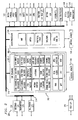
- FIG. 1 shows a multithreaded processor 102 in accordance with the invention.
- the multithreaded processor 102 includes, among other elements, a multithreaded cache memory 110, a multithreaded data memory 112, an instruction decoder 116, a register file 118, and a memory management unit (MMU) 120.
- the multithreaded cache memory 110 is also referred to herein as a multithreaded cache.
- Each thread thus has a corresponding thread cache associated therewith in the multithreaded cache 110.
- the data memory 112 includes N distinct data memory instances, denoted data memories 112-1, 112-2, ... 112-N as shown.
- the processor 102 may implement token triggered multithreading, such as that described in the above-cited U.S. Patent Application Attorney Docket No. 1007-8, entitled “Method and Apparatus for Token Triggered Multithreading.”
- the token triggered threading typically assigns different tokens to each of a plurality of threads of the processor.
- the token triggered threading may utilize a token to identify in association with a current processor clock cycle a particular one of the threads of the processor that will be permitted to issue an instruction for a subsequent clock cycle.
- Other types of threading may also or alternatively be used.
- Each of the thread caches in the multithreaded cache 110 may comprise a memory array having one or more sets of memory locations.
- a given thread cache may further comprise a thread identifier register for storing an associated thread identifier.
- the multithreaded cache 110 interfaces with a main memory (not shown) external to the processor 102 via the MMU 120.
- the MMU 120 like the cache 110, includes a separate instance for the each of the N threads supported by the processor.
- the MMU 120 ensures that the appropriate instructions from main memory are loaded into the multithreaded cache 110.
- the MMU 120 which may comprise or otherwise have associated therewith a cache controller, may implement at least a portion of an address mapping technique, such as fully associative mapping, direct mapping or set-associative mapping. Illustrative set-associative mapping techniques suitable for use in conjunction with the present invention are described in U.S. Patent Application Serial Nos. 10/161,774 and 10/161,874, both filed June 4, 2002 and commonly assigned with the present application, and both of which are incorporated by reference herein.
- the data memory 112 is also typically directly connected to the above-noted external main memory, although this connection is also not explicitly shown in the figure. Also associated with the data memory 112 is a data buffer 130.
- the multithreaded cache 110 is used to store instructions to be executed by the multithreaded processor 102, while the data memory 112 stores data that is operated on by the instructions. Instructions are fetched from the multithreaded cache 110 by the instruction decoder 116 and decoded. Depending upon the instruction type, the instruction decoder 116 may forward a given instruction or associated information to various other units within the processor, as will be described below.
- the processor 102 further includes a set of auxiliary registers 132, which in this example comprise control registers (CRs) 134, link registers (LRs) 136, and counter registers (CTRs) 138.
- auxiliary registers assist in program control flow by modifying the location of instructions that are fetched.
- CRs control registers
- LRs link registers
- CTRs counter registers
- Other registers within the processor 102 include branch register 140 and program counter (PC) registers 142. Like the auxiliary registers 134, 136 and 138, the program counter registers 142 include one instance for each of the threads.
- the branch register 140 receives instructions from the instruction decoder 116, and in conjunction with the program counter registers 142 provide input to an ADD block 144. Elements 140, 142 and 144 collectively comprise a branch unit of the processor 102. The branch unit controls the fetching of instructions in an instruction pipeline implemented by the processor.
- the register file 118 provides temporary storage of integer results. Instructions forwarded from the instruction decoder 116 to an integer instruction queue (IQ) 150 are decoded and the proper hardware thread unit is selected through the use of an offset unit 152 which is shown as including a separate instance for each of the threads.
- the offset unit 152 inserts explicit bits into register file addresses so that independent thread data is not corrupted. For a given thread, these explicit bits may comprise, e.g., a corresponding thread identifier.
- the register file 118 is coupled to input registers RA and RB, the outputs of which are coupled to an ADD block 154.
- the input registers RA and RB are used in implementing instruction pipelining.
- the output of the ADD block 154 is coupled to the data memory 112.
- the register file 118, integer instruction queue 150, offset unit 152, elements RA and RB, and addition element 154 collectively comprise an exemplary integer unit in accordance with the invention.
- Instruction types executable in the processor 102 include Branch, Load, Store, Integer and Vector/SIMD instruction types. If a given instruction does not specify a Branch, Load, Store or Integer operation, it is a Vector/SIMD instruction. Other instruction types can also or alternatively be used. These Integer and Vector/SIMD instruction types are examples of what are more generally referred to herein as integer and vector instruction types, respectively.
- a vector IQ 156 receives vector/SIMD instructions forwarded from the instruction decoder 116.
- a corresponding offset unit 158 shown as including a separate instance for each of the threads, serves to insert the appropriate bits to ensure that independent thread data is not corrupted.
- a vector unit 160 of the processor 102 is separated into N distinct parallel portions, and includes a vector file 162 which is similarly divided.
- the vector file 162 serves substantially the same purpose as the register file 118 except that the former operates on Vector/SIMD instruction types.
- the vector unit 160 illustratively comprises the vector instruction queue 156, the offset unit 158, the vector file 162, and the arithmetic and storage elements associated therewith.
- the operation of the vector unit 160 is as follows.
- a given Vector/SIMD data block encoded either as a fractional or integer data type is read from the vector file 162 and is stored into architecturally visible registers VRABC. From there, the flow proceeds through MPY blocks that perform parallel concurrent multiplication of the Vector/SIMD data. The results are placed in the architecturally visible registers PABC. The ADD units then can perform additional arithmetic operations and place the results in Accumulator (ACC) registers. From there, the data proceeds through a reduction unit 164 where the results are summed in parallel but produce serial semantics.
- the serial semantics provide an output which is substantially the same as that which would be produced if the four saturating values computed in parallel in vector unit 160 were instead computed serially. Such an output is also referred to herein as a serial output.
- the resulting reduced sum is placed in a saturation register denoted SAT.
- the reduction unit 164 and other portions of the vector unit 160 may be implemented using techniques similar to those described in N. Yadav, M. Schulte and J. Glossner, "Parallel Saturating Fractional Arithmetic Units," Proceedings of the 9th Great Lakes Symposium on VLSI, pp. 172-179, Ann Arbor, Michigan, March 4-6, 1999 , which is incorporated by reference herein.
- reduction unit 164 may be implemented as a separate element.
- the processor 102 preferably utilizes pipelined instruction processing.
- the processor 102 may utilize an instruction pipeline in which each thread issues a single instruction per processor clock cycle.
- the instruction pipeline may be configured such that each thread issues multiple instructions per processor clock cycle. More specifically, with a sufficient number of threads and appropriate pipelining, each thread of the processor may issue both a load instruction and a vector multiply instruction in a given processor clock cycle without stalling any of the threads.
- the processor 102 as shown in FIG. 1 is capable of efficiently executing a variety of different types of instruction code, including RISC-based control code, DSP code, Java code and network processing code.
- the processor 102 is therefore particularly well-suited for implementation in a convergence device such as a 3GPP WCDMA mobile unit.
- FIG. 2 shows an example processing system 200 in which the processor 102 may be implemented.
- the processing system 200 may be viewed, for example, as an element of a convergence device such as the above-noted 3GPP WCDMA mobile unit.
- the processing system 200 in this embodiment is configured to support both WCDMA and Global System for Mobile Communication (GSM) wireless communication, as well as processing of voice, data, audio, video and other information communicated over a variety of different media.
- GSM Global System for Mobile Communication
- the processing system 200 includes DSP firmware 202 and a microprocessor 204.
- the DSP firmware 202 is shown as comprising first and second instances denoted 202-1 and 202-2.
- the DSP firmware is coupled to an associated internal memory 206.
- the microprocessor 208 is coupled to an associated internal memory 208.
- the memories 206, 208 are referred to as "internal" in that they are internal to the processing system 200, and both may represent portions of a common memory.
- the DSP firmware 202 and microprocessor 204 may also each communicate with one or more external memories, which are not shown.
- the DSP firmware 202 and microprocessor 204 are preferably both implemented using a single multithreaded processor configured as shown in FIG. 1 .
- Other configurations e.g., configurations based on multiple processors, can also be used.
- the first instance 202-1 of the DSP firmware 202 illustratively includes a plurality of processing elements including a GSM channel equalizer, a GSM channel coder, a GSM burst builder, a GSM channel decoder, a GSM voice decoder, a GSM voice encoder, a GSM transmitter, ciphering/deciphering, timing control, a WCDMA transmitter, filtering, gain and frequency control, a WCDMA searcher, a Rake receiver, a channel encoder, a WCDMA voice decoder, a WCDMA voice encoder, and a channel decoder.
- WMA Windows ® Media Audio
- JPEG/JPEG2000 Joint Photographic Experts Group
- MP3 Moving Picture Experts Group Layer-3 Audio
- AAC Advanced Audio Coding
- MIDI Musical Instrument Digital Interface
- the second instance 202-2 of the DSP firmware 202 may be similarly configured, or may include other processing elements suitable for other supporting other communication functions in the processing system 200.
- the microprocessor 204 illustratively comprises a number of processing elements, including man-machine interface (MMI), Moving Picture Experts Group 4 (MPEG4), protocol stack, Short Message Service/Messaging Management System (SMS/MMS), and real time operating system (OS) elements as shown. Again, the operation of such elements is well understood in the art.
- MMI man-machine interface
- MPEG4 Moving Picture Experts Group 4
- SMS/MMS Short Message Service/Messaging Management System
- OS real time operating system
- the processing system 200 further includes communication bus 210 coupled between DSP firmware 202, microprocessor 204 and system elements 212. Similarly, communication bus 214 is coupled between DSP firmware 202 and system elements 216.
- the system elements 212 include a digital camera, a video camera, Universal Serial Bus (USB), Universal Asynchronous Receiver/Transmitters (UARTS), SCSI Parallel Interface (SPI), Intelligent Interface Controller (I2C), General Purpose I/O (GPIO), Security Identity Module/Universal Subscriber Identity Module (SIM/USIM), external memory I/O, a keypad, an LCD, an interrupt controller, and a Direct Memory Access (DMA) controller.
- USB Universal Serial Bus
- UARTS Universal Asynchronous Receiver/Transmitters
- SPI Serial Interface
- I2C Intelligent Interface Controller
- GPIO General Purpose I/O
- SIM/USIM Security Identity Module/Universal Subscriber Identity Module
- external memory I/O a keypad, an LCD, an interrupt controller, and a Direct Memory Access (DMA) controller.
- DMA Direct Memory Access
- the system elements 216 include receiver I/O, transmitter I/O, and Bluetooth I/O.
- DSP firmware 202 and microprocessor 204 may both be executed on a single multithreaded processor such as multithreaded processor 102.
- the multithreaded processor 102 may thus be utilized to execute code associated with the system elements 212, 216, 218, 220 and 222, as well as code associated with the processing elements of DSP firmware 202 and microprocessor 204.
- the microprocessor 204 in the processing system 200 may be utilize to run code associated with high-level applications.
- the processing elements associated with the D SP firmware 202 may be implemented utilizing software compilation.
- software compilation enables the efficient translation of high-level programming languages.
- FIGS. 1 and 2 are simplified for clarity of illustration, and additional or alternative elements not explicitly shown may be included.
Abstract
Description
- The present application claims the priority of
U.S. Provisional Application Serial No. 60/341,289 filed December 20, 2001 - The present invention is related to the inventions described in U.S. Patent Applications Attorney Docket No. 1007-5, entitled "Method and Apparatus for Thread-Based Memory Access in a Multithreaded Processor," Attorney Docket No. 1007-7, entitled "Method and Apparatus for Register File Port Reduction in a Multithreaded Processor," and Attorney Docket No. 1007-8, entitled "Method and Apparatus for Token Triggered Multithreading," all of which are filed concurrently herewith and incorporated by reference herein.
- The present invention relates generally to the field of digital data processors, and more particularly to multithreaded processors.
- Multithreaded processors are processors that support simultaneous execution of multiple distinct instruction sequences or "threads." Conventional threading techniques are described in, for example, M.J. Flynn, "Computer Architecture: Pipelined and Parallel Processor Design," Jones and Bartlett Publishers, Boston, MA, 1995, and G.A. Blaauw and Frederick P. Brooks, "Computer Architecture: Concepts and Evolution," Addison-Wesley, Reading, Massachusetts, 1997, both of which are incorporated by reference herein.
- Existing multithreaded processors are generally not optimized for use in convergence devices, which may include devices configured for processing of voice, data, audio, video and other information communicated over a variety of different media. Such devices will typically require execution of a number of different types of code, including digital signal processor (DSP) code associated with signal processing operations as well high-level program application code written in Java or another object-oriented programming language. A more particular example of a convergence device of this type is a wireless mobile unit of a recently-developed high-speed CDMA communication system such as the 3rd Generation Partnership Project (3GPP) Wideband CDMA
- (WCDMA) system, described in 3GPP Technical Specifications TS 25. 1xx, which are incorporated by reference herein.
- A need therefore exists for an improved multithreaded processor that is particularly well-suited for use in a convergence device.
- The present invention provides an improved multithreaded processor which in an illustrative embodiment is capable of efficiently executing RISC-based control code, DSP code, Java code and network processing code, and is thus particularly well-suited for use in a 3 GPP WCDMA mobile unit or other convergence device.
- In accordance with one aspect of the invention, a multithreaded processor includes an instruction decoder for decoding retrieved instructions to determine an instruction type for each of the retrieved instructions, an integer unit coupled to the instruction decoder for processing integer type instructions, and a vector unit coupled to the instruction decoder for processing vector type instructions. A reduction unit is preferably associated with the vector unit and receives parallel data elements processed in the vector unit. The reduction unit generates a serial output from the parallel data elements. The processor is preferably configured to utilize token triggered threading in conjunction with instruction pipelining.
-
-
FIG. 1 is a block diagram of an illustrative embodiment of a multithreaded processor in accordance with the invention. -
FIG. 2 is a block diagram illustrating one possible implementation of a processing system incorporating the multithreaded processor ofFIG. 1 . - The present invention will be illustrated herein in conjunction with an exemplary multithreaded processor and corresponding processing system. It should be understood, however, that the invention does not require the use of the particular multithreaded processor and processing system configurations of the illustrative embodiments, and is more generally suitable for use in any multithreaded processor or information processing system application in which it is desirable to provide improved processor performance. In addition, although particularly well-suited for use in convergence devices, the multithreaded processor of the present invention can be used in other types of devices.
- As will be described in greater detail below, an illustrative embodiment of a multithreaded processor in accordance with the present invention is capable of executing RISC-based control code, digital signal processor (DSP) code, Java code and network processing code. The processor includes a single instruction multiple data (SIMD) vector unit, a reduction unit, and long instruction word (LIW) compounded instruction execution.
-
FIG. 1 shows amultithreaded processor 102 in accordance with the invention. Themultithreaded processor 102 includes, among other elements, amultithreaded cache memory 110, a multithreaded data memory 112, aninstruction decoder 116, aregister file 118, and a memory management unit (MMU) 120. The multithreadedcache memory 110 is also referred to herein as a multithreaded cache. - The
multithreaded cache 110 includes a plurality of thread caches 110-1, 110-2, ... 110-N, where N generally denotes the number of threads supported by themultithreaded processor 102, and in this particular example is given by N = 4. Of course, other values of N may be used, as will be readily apparent to those skilled in the art. - Each thread thus has a corresponding thread cache associated therewith in the
multithreaded cache 110. Similarly, the data memory 112 includes N distinct data memory instances, denoted data memories 112-1, 112-2, ... 112-N as shown. - The
processor 102 may implement token triggered multithreading, such as that described in the above-cited U.S. Patent Application Attorney Docket No. 1007-8, entitled "Method and Apparatus for Token Triggered Multithreading." The token triggered threading typically assigns different tokens to each of a plurality of threads of the processor. For example, the token triggered threading may utilize a token to identify in association with a current processor clock cycle a particular one of the threads of the processor that will be permitted to issue an instruction for a subsequent clock cycle. Other types of threading may also or alternatively be used. - Each of the thread caches in the
multithreaded cache 110 may comprise a memory array having one or more sets of memory locations. A given thread cache may further comprise a thread identifier register for storing an associated thread identifier. - The
multithreaded cache 110 interfaces with a main memory (not shown) external to theprocessor 102 via the MMU 120. The MMU 120, like thecache 110, includes a separate instance for the each of the N threads supported by the processor. TheMMU 120 ensures that the appropriate instructions from main memory are loaded into themultithreaded cache 110. The MMU 120, which may comprise or otherwise have associated therewith a cache controller, may implement at least a portion of an address mapping technique, such as fully associative mapping, direct mapping or set-associative mapping. Illustrative set-associative mapping techniques suitable for use in conjunction with the present invention are described inU.S. Patent Application Serial Nos. 10/161,774 and10/161,874, both filed June 4, 2002 - The data memory 112 is also typically directly connected to the above-noted external main memory, although this connection is also not explicitly shown in the figure. Also associated with the data memory 112 is a
data buffer 130. - Techniques for thread-based banking of the
multithreaded cache 110, the data memory 112 or other memories associated with a multithreaded processor are described in the above-cited U.S. Patent Application Attorney Docket No. 1007-5, entitled "Method and Apparatus for Thread-Based Memory Access in a Multithreaded Processor." - In general, the
multithreaded cache 110 is used to store instructions to be executed by themultithreaded processor 102, while the data memory 112 stores data that is operated on by the instructions. Instructions are fetched from themultithreaded cache 110 by theinstruction decoder 116 and decoded. Depending upon the instruction type, theinstruction decoder 116 may forward a given instruction or associated information to various other units within the processor, as will be described below. - The
processor 102 further includes a set ofauxiliary registers 132, which in this example comprise control registers (CRs) 134, link registers (LRs) 136, and counter registers (CTRs) 138. These auxiliary registers assist in program control flow by modifying the location of instructions that are fetched. As illustrated in the figure, there is one instance of each of theauxiliary registers - Other registers within the
processor 102 includebranch register 140 and program counter (PC)registers 142. Like theauxiliary registers program counter registers 142 include one instance for each of the threads. Thebranch register 140 receives instructions from theinstruction decoder 116, and in conjunction with theprogram counter registers 142 provide input to anADD block 144.Elements processor 102. The branch unit controls the fetching of instructions in an instruction pipeline implemented by the processor. - The
register file 118 provides temporary storage of integer results. Instructions forwarded from theinstruction decoder 116 to an integer instruction queue (IQ) 150 are decoded and the proper hardware thread unit is selected through the use of anoffset unit 152 which is shown as including a separate instance for each of the threads. The offsetunit 152 inserts explicit bits into register file addresses so that independent thread data is not corrupted. For a given thread, these explicit bits may comprise, e.g., a corresponding thread identifier. - As shown in the figure, the
register file 118 is coupled to input registers RA and RB, the outputs of which are coupled to anADD block 154. The input registers RA and RB are used in implementing instruction pipelining. The output of theADD block 154 is coupled to the data memory 112. - The
register file 118,integer instruction queue 150, offsetunit 152, elements RA and RB, andaddition element 154 collectively comprise an exemplary integer unit in accordance with the invention. - Techniques for thread-based access to a register file such as
register file 118 are described in the above-cited U.S. Patent Application Attorney Docket No. 1007-7, entitled "Method and Apparatus for Register File Port Reduction in a Multithreaded Processor." - Instruction types executable in the
processor 102 include Branch, Load, Store, Integer and Vector/SIMD instruction types. If a given instruction does not specify a Branch, Load, Store or Integer operation, it is a Vector/SIMD instruction. Other instruction types can also or alternatively be used. These Integer and Vector/SIMD instruction types are examples of what are more generally referred to herein as integer and vector instruction types, respectively. - A
vector IQ 156 receives vector/SIMD instructions forwarded from theinstruction decoder 116. A corresponding offsetunit 158, shown as including a separate instance for each of the threads, serves to insert the appropriate bits to ensure that independent thread data is not corrupted. - A
vector unit 160 of theprocessor 102 is separated into N distinct parallel portions, and includes avector file 162 which is similarly divided. Thevector file 162 serves substantially the same purpose as theregister file 118 except that the former operates on Vector/SIMD instruction types. - The
vector unit 160 illustratively comprises thevector instruction queue 156, the offsetunit 158, thevector file 162, and the arithmetic and storage elements associated therewith. - The operation of the
vector unit 160 is as follows. A given Vector/SIMD data block encoded either as a fractional or integer data type is read from thevector file 162 and is stored into architecturally visible registers VRABC. From there, the flow proceeds through MPY blocks that perform parallel concurrent multiplication of the Vector/SIMD data. The results are placed in the architecturally visible registers PABC. The ADD units then can perform additional arithmetic operations and place the results in Accumulator (ACC) registers. From there, the data proceeds through areduction unit 164 where the results are summed in parallel but produce serial semantics. The serial semantics provide an output which is substantially the same as that which would be produced if the four saturating values computed in parallel invector unit 160 were instead computed serially. Such an output is also referred to herein as a serial output. The resulting reduced sum is placed in a saturation register denoted SAT. - The
reduction unit 164 and other portions of thevector unit 160 may be implemented using techniques similar to those described in N. Yadav, M. Schulte and J. Glossner, "Parallel Saturating Fractional Arithmetic Units," Proceedings of the 9th Great Lakes Symposium on VLSI, pp. 172-179, Ann Arbor, Michigan, March 4-6, 1999, which is incorporated by reference herein. - Although shown as part of
vector unit 160 in the illustrative embodiment,reduction unit 164 may be implemented as a separate element. - The
processor 102 preferably utilizes pipelined instruction processing. For example, theprocessor 102 may utilize an instruction pipeline in which each thread issues a single instruction per processor clock cycle. As another example, the instruction pipeline may be configured such that each thread issues multiple instructions per processor clock cycle. More specifically, with a sufficient number of threads and appropriate pipelining, each thread of the processor may issue both a load instruction and a vector multiply instruction in a given processor clock cycle without stalling any of the threads. - Advantageously, the
processor 102 as shown inFIG. 1 is capable of efficiently executing a variety of different types of instruction code, including RISC-based control code, DSP code, Java code and network processing code. Theprocessor 102 is therefore particularly well-suited for implementation in a convergence device such as a 3GPP WCDMA mobile unit. -
FIG. 2 shows anexample processing system 200 in which theprocessor 102 may be implemented. Theprocessing system 200 may be viewed, for example, as an element of a convergence device such as the above-noted 3GPP WCDMA mobile unit. - More specifically, the
processing system 200 in this embodiment is configured to support both WCDMA and Global System for Mobile Communication (GSM) wireless communication, as well as processing of voice, data, audio, video and other information communicated over a variety of different media. - The
processing system 200 includesDSP firmware 202 and amicroprocessor 204. TheDSP firmware 202 is shown as comprising first and second instances denoted 202-1 and 202-2. The DSP firmware is coupled to an associatedinternal memory 206. Themicroprocessor 208 is coupled to an associatedinternal memory 208. Thememories processing system 200, and both may represent portions of a common memory. TheDSP firmware 202 andmicroprocessor 204 may also each communicate with one or more external memories, which are not shown. - The
DSP firmware 202 andmicroprocessor 204 are preferably both implemented using a single multithreaded processor configured as shown inFIG. 1 . Other configurations, e.g., configurations based on multiple processors, can also be used. - The first instance 202-1 of the
DSP firmware 202 illustratively includes a plurality of processing elements including a GSM channel equalizer, a GSM channel coder, a GSM burst builder, a GSM channel decoder, a GSM voice decoder, a GSM voice encoder, a GSM transmitter, ciphering/deciphering, timing control, a WCDMA transmitter, filtering, gain and frequency control, a WCDMA searcher, a Rake receiver, a channel encoder, a WCDMA voice decoder, a WCDMA voice encoder, and a channel decoder. Other elements include Windows® Media Audio (WMA), Real Media, Joint Photographic Experts Group (JPEG/JPEG2000), Moving Picture Experts Group Layer-3 Audio (MP3), Advanced Audio Coding (AAC) and Musical Instrument Digital Interface (MIDI). The operation of such elements is well understood in the art and therefore not described in further detail herein. - The second instance 202-2 of the
DSP firmware 202 may be similarly configured, or may include other processing elements suitable for other supporting other communication functions in theprocessing system 200. - The
microprocessor 204 illustratively comprises a number of processing elements, including man-machine interface (MMI), Moving Picture Experts Group 4 (MPEG4), protocol stack, Short Message Service/Messaging Management System (SMS/MMS), and real time operating system (OS) elements as shown. Again, the operation of such elements is well understood in the art. - The
processing system 200 further includescommunication bus 210 coupled betweenDSP firmware 202,microprocessor 204 andsystem elements 212. Similarly,communication bus 214 is coupled betweenDSP firmware 202 andsystem elements 216. - The
system elements 212 include a digital camera, a video camera, Universal Serial Bus (USB), Universal Asynchronous Receiver/Transmitters (UARTS), SCSI Parallel Interface (SPI), Intelligent Interface Controller (I2C), General Purpose I/O (GPIO), Security Identity Module/Universal Subscriber Identity Module (SIM/USIM), external memory I/O, a keypad, an LCD, an interrupt controller, and a Direct Memory Access (DMA) controller. - The
system elements 216 include receiver I/O, transmitter I/O, and Bluetooth I/O. - Other system elements shown in the figure include test input/output (I/O) 218, system clock and
control 220, andpower management 222. - The operation of the
system elements - As noted above, the functions associated with both
DSP firmware 202 andmicroprocessor 204 may both be executed on a single multithreaded processor such asmultithreaded processor 102. Themultithreaded processor 102 may thus be utilized to execute code associated with thesystem elements DSP firmware 202 andmicroprocessor 204. - The
microprocessor 204 in theprocessing system 200 may be utilize to run code associated with high-level applications. - The processing elements associated with the
D SP firmware 202 may be implemented utilizing software compilation. Advantageously, software compilation enables the efficient translation of high-level programming languages. - It should be emphasized that the present invention does not require the particular multithreaded processor and processing system configurations shown in
FIGS. 1 and2 , respectively. As indicated previously, the invention can be implemented in a wide variety of other multithreaded processor and processing system configurations. - Moreover, it is to be appreciated that the particular arrangements shown in
FIGS. 1 and2 are simplified for clarity of illustration, and additional or alternative elements not explicitly shown may be included. - The above-described embodiments of the invention are thus intended to be illustrative only, and numerous alternative embodiments within the scope of the appended claims will be apparent to those skilled in the art.
Claims (16)
- A multithreaded processor comprising:an instruction decoder for decoding instructions to determine an instruction type for each of at least a subset of the instructions;an integer unit coupled to the instruction decoder for processing integer type instructions received from the instruction decoder; anda vector unit coupled to the instruction decoder for processing vector type instructions received from the instruction decoder,wherein either the integer unit or the vector unit further comprises an instruction queue having an input coupled to an output of the instruction decoder, a file having an input coupled to an output of the instruction queue, an offset unit having an output coupled to an input of the file, and an arithmetic element having at least one input coupled to an output of the file.
- The multithreaded processor of claim 1, wherein the integer unit comprises the instruction queue, the file, the offset unit, and the arithmetic element, and wherein the arithmetic element comprises an addition element.
- The multithreaded processor of claim 1, wherein the vector unit comprises the instruction queue, the file, the offset unit, and the arithmetic element, and wherein the arithmetic element comprises a multiplier element.
- The multithreaded processor of claim 1, further comprising a reduction unit associated with the vector unit, wherein the reduction unit is configured to receive parallel data elements processed in the vector unit, and wherein the reduction unit is configured to generate a serial output from the parallel data elements.
- The multithreaded processor of claim 1, wherein the instruction decoder is configured to retrieve the instructions from a multithreaded cache memory of the multithreaded processor, the multithreaded cache memory comprising a thread cache for each of a plurality of threads of the processor.
- The multithreaded processor of claim 1, wherein the offset unit comprises a separate instance for each of a plurality of threads supported by the processor.
- The multithreaded processor of claim 1, wherein the processor is configured to support at least branch, load, store, integer and vector instruction types.
- The multithreaded processor of claim 7, wherein the vector instruction types comprise at least a single issue multiple dispatch instruction type.
- The multithreaded processor of claim 1, wherein the processor is configured to execute at least two of the following: control code, digital signal processor (DSP) code, Java code and network processing code.
- The multithreaded processor of claim 1, wherein the processor is configured for pipelined instruction processing.
- The multithreaded processor of claim 10, wherein the processor utilizes an instruction pipeline in which each thread issues a single instruction per processor clock cycle.
- The multithreaded processor of claim 10, wherein the processor utilizes an instruction pipeline in which each thread issues multiple instructions per processor clock cycle.
- The multithreaded processor of claim 12, wherein each of a plurality of threads of the processor issues both a load instruction and a vector multiply instruction in each of a corresponding plurality of processor clock cycles without stalling of any of the plurality of threads.
- A method comprising:decoding instructions to determine an instruction type for each of at least a subset of the instructions;processing, by an integer unit, integer type instructions received from the instruction decoder; andprocessing, by a vector unit, vector type instructions received from the instruction decoder,wherein either the integer unit or the vector unit further comprises an instruction queue having an input coupled to an output of the instruction decoder, a file having an input coupled to an output of the instruction queue, an offset unit having an output coupled to an input of the file, and an arithmetic element having at least one input coupled to an output of the file.
- The method of claim 14, wherein the integer unit comprises the instruction queue, the file, the offset unit, and the arithmetic element, and wherein the arithmetic element comprises an addition element.
- The method of claim 14, wherein the vector unit comprises the instruction queue, the file, the offset unit, and the arithmetic element, and wherein the arithmetic element comprises a multiplier element.
Applications Claiming Priority (3)
| Application Number | Priority Date | Filing Date | Title |
|---|---|---|---|
| US34128901P | 2001-12-20 | 2001-12-20 | |
| US10/269,372 US6968445B2 (en) | 2001-12-20 | 2002-10-11 | Multithreaded processor with efficient processing for convergence device applications |
| EP02799229A EP1468367A4 (en) | 2001-12-20 | 2002-12-11 | Multithreaded processor with efficient processing for convergence device applications |
Related Parent Applications (1)
| Application Number | Title | Priority Date | Filing Date |
|---|---|---|---|
| EP02799229.6 Division | 2002-12-11 |
Publications (2)
| Publication Number | Publication Date |
|---|---|
| EP2259190A2 true EP2259190A2 (en) | 2010-12-08 |
| EP2259190A3 EP2259190A3 (en) | 2011-06-15 |
Family
ID=26953660
Family Applications (4)
| Application Number | Title | Priority Date | Filing Date |
|---|---|---|---|
| EP10181448A Withdrawn EP2261814A3 (en) | 2001-12-20 | 2002-12-11 | Multithreaded processor with efficient processing for convergence device applications |
| EP10181445A Ceased EP2259190A3 (en) | 2001-12-20 | 2002-12-11 | Multithreaded processor with efficient processing for convergence device applications |
| EP02799229A Ceased EP1468367A4 (en) | 2001-12-20 | 2002-12-11 | Multithreaded processor with efficient processing for convergence device applications |
| EP10181450A Ceased EP2261815A3 (en) | 2001-12-20 | 2002-12-11 | Multithread processor with efficient processing for convergence device applications |
Family Applications Before (1)
| Application Number | Title | Priority Date | Filing Date |
|---|---|---|---|
| EP10181448A Withdrawn EP2261814A3 (en) | 2001-12-20 | 2002-12-11 | Multithreaded processor with efficient processing for convergence device applications |
Family Applications After (2)
| Application Number | Title | Priority Date | Filing Date |
|---|---|---|---|
| EP02799229A Ceased EP1468367A4 (en) | 2001-12-20 | 2002-12-11 | Multithreaded processor with efficient processing for convergence device applications |
| EP10181450A Ceased EP2261815A3 (en) | 2001-12-20 | 2002-12-11 | Multithread processor with efficient processing for convergence device applications |
Country Status (6)
| Country | Link |
|---|---|
| US (1) | US6968445B2 (en) |
| EP (4) | EP2261814A3 (en) |
| JP (1) | JP2005514678A (en) |
| KR (1) | KR100942668B1 (en) |
| AU (1) | AU2002364154A1 (en) |
| WO (1) | WO2003054714A1 (en) |
Families Citing this family (33)
| Publication number | Priority date | Publication date | Assignee | Title |
|---|---|---|---|---|
| DE10206830B4 (en) * | 2002-02-18 | 2004-10-14 | Systemonic Ag | Method and arrangement for merging data from parallel data paths |
| US7360220B2 (en) * | 2002-10-31 | 2008-04-15 | Intel Corporation | Methods and apparatus for multi-threading using differently coded software segments to perform an algorithm |
| US7593978B2 (en) * | 2003-05-09 | 2009-09-22 | Sandbridge Technologies, Inc. | Processor reduction unit for accumulation of multiple operands with or without saturation |
| TW200518070A (en) | 2003-10-10 | 2005-06-01 | Matsushita Electric Ind Co Ltd | Recording medium, reproduction device, program, and reproduction method |
| US7251737B2 (en) * | 2003-10-31 | 2007-07-31 | Sandbridge Technologies, Inc. | Convergence device with dynamic program throttling that replaces noncritical programs with alternate capacity programs based on power indicator |
| US7349938B2 (en) * | 2004-03-05 | 2008-03-25 | Sandbridge Technologies, Inc. | Arithmetic circuit with balanced logic levels for low-power operation |
| US20050243059A1 (en) * | 2004-03-16 | 2005-11-03 | Morris Martin G | High-reliability computer interface for wireless input devices |
| US7475222B2 (en) * | 2004-04-07 | 2009-01-06 | Sandbridge Technologies, Inc. | Multi-threaded processor having compound instruction and operation formats |
| US8074051B2 (en) * | 2004-04-07 | 2011-12-06 | Aspen Acquisition Corporation | Multithreaded processor with multiple concurrent pipelines per thread |
| US7797363B2 (en) * | 2004-04-07 | 2010-09-14 | Sandbridge Technologies, Inc. | Processor having parallel vector multiply and reduce operations with sequential semantics |
| US7302554B2 (en) * | 2004-04-22 | 2007-11-27 | Sony Computer Entertainment Inc. | Methods and apparatus for multi-processor pipeline parallelism |
| US7672409B2 (en) * | 2004-07-23 | 2010-03-02 | Sandbridge Technologies, Inc. | Base station software for multi-user detection uplinks and downlinks and method thereof |
| TW200625097A (en) * | 2004-11-17 | 2006-07-16 | Sandbridge Technologies Inc | Data file storing multiple date types with controlled data access |
| GB2423604B (en) * | 2005-02-25 | 2007-11-21 | Clearspeed Technology Plc | Microprocessor architectures |
| US8024549B2 (en) * | 2005-03-04 | 2011-09-20 | Mtekvision Co., Ltd. | Two-dimensional processor array of processing elements |
| DE102005030055B4 (en) * | 2005-06-27 | 2007-04-12 | Webasto Ag | Sunroof for vehicles has side skirt arranged adjacent seal provided close to upper end of guide rail or at edge of opening |
| WO2007033203A2 (en) | 2005-09-13 | 2007-03-22 | Freescale Semiconductor Inc. | Multi-threaded processor architecture |
| US7631171B2 (en) * | 2005-12-19 | 2009-12-08 | Sun Microsystems, Inc. | Method and apparatus for supporting vector operations on a multi-threaded microprocessor |
| JP2009523292A (en) * | 2006-01-10 | 2009-06-18 | ブライトスケール インコーポレイテッド | Method and apparatus for scheduling multimedia data processing in parallel processing systems |
| EP1858261A1 (en) * | 2006-05-16 | 2007-11-21 | Ascom (Schweiz) AG | Real-time transmission of video data |
| WO2008027567A2 (en) * | 2006-09-01 | 2008-03-06 | Brightscale, Inc. | Integral parallel machine |
| WO2008070250A2 (en) * | 2006-09-26 | 2008-06-12 | Sandbridge Technologies Inc. | Software implementation of matrix inversion in a wireless communication system |
| WO2008060948A2 (en) * | 2006-11-10 | 2008-05-22 | Sandbridge Technologies, Inc. | Method and system for parallelization of pipelined computations |
| CN100465941C (en) * | 2007-10-30 | 2009-03-04 | 中国传媒大学 | Paralleling calculating machinery based on DSP and system |
| WO2009061547A1 (en) * | 2007-11-05 | 2009-05-14 | Sandbridge Technologies, Inc. | Method of encoding register instruction fields |
| KR20100120133A (en) * | 2008-01-30 | 2010-11-12 | 샌드브리지 테크놀로지스, 인코포레이티드 | Method for enabling multi-processor synchronization |
| EP2266038A4 (en) * | 2008-03-13 | 2011-09-21 | Aspen Acquisition Corp | Method for achieving power savings by disabling a valid array |
| US20090276448A1 (en) * | 2008-04-30 | 2009-11-05 | International Business Machines Corporation | Parallel transformation of files |
| EP2324430A4 (en) | 2008-08-06 | 2012-07-25 | Aspen Acquisition Corp | Haltable and restartable dma engine |
| JP6020091B2 (en) | 2012-11-27 | 2016-11-02 | 富士通株式会社 | Arithmetic processing device control program, arithmetic processing device control method, and arithmetic processing device |
| US9870340B2 (en) | 2015-03-30 | 2018-01-16 | International Business Machines Corporation | Multithreading in vector processors |
| CN114546492A (en) * | 2015-04-24 | 2022-05-27 | 优创半导体科技有限公司 | Computer processor implementing pre-translation of virtual addresses using target registers |
| US10891991B2 (en) * | 2018-11-26 | 2021-01-12 | Gsi Technology Inc. | Massively parallel, associative multiplier accumulator |
Citations (1)
| Publication number | Priority date | Publication date | Assignee | Title |
|---|---|---|---|---|
| US5778243A (en) * | 1996-07-03 | 1998-07-07 | International Business Machines Corporation | Multi-threaded cell for a memory |
Family Cites Families (25)
| Publication number | Priority date | Publication date | Assignee | Title |
|---|---|---|---|---|
| DE69131228T2 (en) * | 1990-08-23 | 1999-09-23 | Cray Research Inc | DOUBLE LEVEL SEQUENCE PLANNING OF PROCESSES |
| JPH05204656A (en) * | 1991-11-30 | 1993-08-13 | Toshiba Corp | Method for holding data inherent in thread |
| US5875464A (en) * | 1991-12-10 | 1999-02-23 | International Business Machines Corporation | Computer system with private and shared partitions in cache |
| US5444853A (en) * | 1992-03-31 | 1995-08-22 | Seiko Epson Corporation | System and method for transferring data between a plurality of virtual FIFO's and a peripheral via a hardware FIFO and selectively updating control information associated with the virtual FIFO's |
| US6128720A (en) | 1994-12-29 | 2000-10-03 | International Business Machines Corporation | Distributed processing array with component processors performing customized interpretation of instructions |
| US5682491A (en) | 1994-12-29 | 1997-10-28 | International Business Machines Corporation | Selective processing and routing of results among processors controlled by decoding instructions using mask value derived from instruction tag and processor identifier |
| US5649135A (en) | 1995-01-17 | 1997-07-15 | International Business Machines Corporation | Parallel processing system and method using surrogate instructions |
| US5659785A (en) | 1995-02-10 | 1997-08-19 | International Business Machines Corporation | Array processor communication architecture with broadcast processor instructions |
| US5822560A (en) * | 1996-05-23 | 1998-10-13 | Advanced Micro Devices, Inc. | Apparatus for efficient instruction execution via variable issue and variable control vectors per issue |
| US5933627A (en) * | 1996-07-01 | 1999-08-03 | Sun Microsystems | Thread switch on blocked load or store using instruction thread field |
| US5909572A (en) * | 1996-12-02 | 1999-06-01 | Compaq Computer Corp. | System and method for conditionally moving an operand from a source register to a destination register |
| US5974538A (en) | 1997-02-21 | 1999-10-26 | Wilmot, Ii; Richard Byron | Method and apparatus for annotating operands in a computer system with source instruction identifiers |
| US6314511B2 (en) | 1997-04-03 | 2001-11-06 | University Of Washington | Mechanism for freeing registers on processors that perform dynamic out-of-order execution of instructions using renaming registers |
| US6079010A (en) | 1998-03-31 | 2000-06-20 | Lucent Technologies Inc. | Multiple machine view execution in a computer system |
| US6292822B1 (en) | 1998-05-13 | 2001-09-18 | Microsoft Corporation | Dynamic load balancing among processors in a parallel computer |
| US6317821B1 (en) | 1998-05-18 | 2001-11-13 | Lucent Technologies Inc. | Virtual single-cycle execution in pipelined processors |
| US6205519B1 (en) | 1998-05-27 | 2001-03-20 | Hewlett Packard Company | Cache management for a multi-threaded processor |
| US6260189B1 (en) | 1998-09-14 | 2001-07-10 | Lucent Technologies Inc. | Compiler-controlled dynamic instruction dispatch in pipelined processors |
| US6256725B1 (en) | 1998-12-04 | 2001-07-03 | Agere Systems Guardian Corp. | Shared datapath processor utilizing stack-based and register-based storage spaces |
| US6269437B1 (en) | 1999-03-22 | 2001-07-31 | Agere Systems Guardian Corp. | Duplicator interconnection methods and apparatus for reducing port pressure in a clustered processor |
| US6282585B1 (en) | 1999-03-22 | 2001-08-28 | Agere Systems Guardian Corp. | Cooperative interconnection for reducing port pressure in clustered microprocessors |
| US6230251B1 (en) | 1999-03-22 | 2001-05-08 | Agere Systems Guardian Corp. | File replication methods and apparatus for reducing port pressure in a clustered processor |
| GB2394815B (en) * | 1999-04-09 | 2004-08-25 | Clearspeed Technology Ltd | Parallel data processing systems |
| US6351808B1 (en) * | 1999-05-11 | 2002-02-26 | Sun Microsystems, Inc. | Vertically and horizontally threaded processor with multidimensional storage for storing thread data |
| US6449719B1 (en) | 1999-11-09 | 2002-09-10 | Widevine Technologies, Inc. | Process and streaming server for encrypting a data stream |
-
2002
- 2002-10-11 US US10/269,372 patent/US6968445B2/en not_active Expired - Lifetime
- 2002-12-11 EP EP10181448A patent/EP2261814A3/en not_active Withdrawn
- 2002-12-11 EP EP10181445A patent/EP2259190A3/en not_active Ceased
- 2002-12-11 EP EP02799229A patent/EP1468367A4/en not_active Ceased
- 2002-12-11 AU AU2002364154A patent/AU2002364154A1/en not_active Abandoned
- 2002-12-11 JP JP2003555361A patent/JP2005514678A/en active Pending
- 2002-12-11 EP EP10181450A patent/EP2261815A3/en not_active Ceased
- 2002-12-11 WO PCT/US2002/039667 patent/WO2003054714A1/en active Application Filing
- 2002-12-11 KR KR1020047009704A patent/KR100942668B1/en active IP Right Grant
Patent Citations (1)
| Publication number | Priority date | Publication date | Assignee | Title |
|---|---|---|---|---|
| US5778243A (en) * | 1996-07-03 | 1998-07-07 | International Business Machines Corporation | Multi-threaded cell for a memory |
Non-Patent Citations (3)
| Title |
|---|
| G.A. BLAAUW; FREDERICK P. BROOKS: "Computer Architecture: Concepts and Evolution", 1997, ADDISON-WESLEY |
| M.J. FLYNN: "Computer Architecture: Pipelined and Parallel Processor Design", 1995, JONES AND BARTLETT PUBLISHERS |
| N. YADAV; M. SCHULTE; J, GLOSSNER: "Proceedings of the 9th Great Lakes Symposium on VLSI", 4 March 1999, ANN ARBOR, article "Parallel Saturating Fractional Arithmetic Units", pages: 172 - 179 |
Also Published As
| Publication number | Publication date |
|---|---|
| EP2261814A3 (en) | 2011-06-15 |
| US6968445B2 (en) | 2005-11-22 |
| JP2005514678A (en) | 2005-05-19 |
| EP2259190A3 (en) | 2011-06-15 |
| EP1468367A4 (en) | 2008-02-13 |
| EP2261815A2 (en) | 2010-12-15 |
| KR20040077860A (en) | 2004-09-07 |
| EP2261815A3 (en) | 2011-06-15 |
| AU2002364154A1 (en) | 2003-07-09 |
| WO2003054714A1 (en) | 2003-07-03 |
| US20030120901A1 (en) | 2003-06-26 |
| EP1468367A1 (en) | 2004-10-20 |
| EP2261814A2 (en) | 2010-12-15 |
| KR100942668B1 (en) | 2010-02-17 |
Similar Documents
| Publication | Publication Date | Title |
|---|---|---|
| US6968445B2 (en) | Multithreaded processor with efficient processing for convergence device applications | |
| US6418527B1 (en) | Data processor instruction system for grouping instructions with or without a common prefix and data processing system that uses two or more instruction grouping methods | |
| WO2001022216A1 (en) | Selective writing of data elements from packed data based upon a mask using predication | |
| US20120204008A1 (en) | Processor with a Hybrid Instruction Queue with Instruction Elaboration Between Sections | |
| US20120284489A1 (en) | Methods and Apparatus for Constant Extension in a Processor | |
| US20150227373A1 (en) | Stop bits and predication for enhanced instruction stream control | |
| US8707013B2 (en) | On-demand predicate registers | |
| EP2577464B1 (en) | System and method to evaluate a data value as an instruction | |
| US7043625B2 (en) | Method and apparatus for adding user-defined execution units to a processor using configurable long instruction word (CLIW) | |
| US20070220235A1 (en) | Instruction subgraph identification for a configurable accelerator | |
| US20120110037A1 (en) | Methods and Apparatus for a Read, Merge and Write Register File | |
| EP2542963B1 (en) | System and method of processing hierarchical very long instruction packets | |
| KR20070118705A (en) | System and method of using a predicate value to access a register file | |
| CN100359506C (en) | Multithreaded processor with efficient processing for convergence device applications | |
| US9021238B2 (en) | System for accessing a register file using an address retrieved from the register file | |
| WO2021061626A1 (en) | Instruction executing method and apparatus | |
| CN117055959A (en) | Reconfigurable finger taking system based on annular queue | |
| JPH02148328A (en) | System for prefetching operand data |
Legal Events
| Date | Code | Title | Description |
|---|---|---|---|
| PUAI | Public reference made under article 153(3) epc to a published international application that has entered the european phase |
Free format text: ORIGINAL CODE: 0009012 |
|
| AC | Divisional application: reference to earlier application |
Ref document number: 1468367 Country of ref document: EP Kind code of ref document: P |
|
| AK | Designated contracting states |
Kind code of ref document: A2 Designated state(s): AT BE BG CH CY CZ DE DK EE ES FI FR GB GR IE IT LI LU MC NL PT SE SI SK TR |
|
| RAP1 | Party data changed (applicant data changed or rights of an application transferred) |
Owner name: ASPEN ACQUISITION CORPORATION |
|
| RIN1 | Information on inventor provided before grant (corrected) |
Inventor name: HOKENEK, ERDEM Inventor name: MOUDGILL, MAYAN Inventor name: GLOSSNER, JOHN, C. |
|
| PUAL | Search report despatched |
Free format text: ORIGINAL CODE: 0009013 |
|
| AK | Designated contracting states |
Kind code of ref document: A3 Designated state(s): AT BE BG CH CY CZ DE DK EE ES FI FR GB GR IE IT LI LU MC NL PT SE SI SK TR |
|
| 17P | Request for examination filed |
Effective date: 20111215 |
|
| 17Q | First examination report despatched |
Effective date: 20120416 |
|
| RAP1 | Party data changed (applicant data changed or rights of an application transferred) |
Owner name: QUALCOMM INCORPORATED |
|
| STAA | Information on the status of an ep patent application or granted ep patent |
Free format text: STATUS: THE APPLICATION HAS BEEN REFUSED |
|
| 18R | Application refused |
Effective date: 20130612 |