EP2242005A1 - Communication device comprising two chips with common communication interface - Google Patents
Communication device comprising two chips with common communication interface Download PDFInfo
- Publication number
- EP2242005A1 EP2242005A1 EP09305326A EP09305326A EP2242005A1 EP 2242005 A1 EP2242005 A1 EP 2242005A1 EP 09305326 A EP09305326 A EP 09305326A EP 09305326 A EP09305326 A EP 09305326A EP 2242005 A1 EP2242005 A1 EP 2242005A1
- Authority
- EP
- European Patent Office
- Prior art keywords
- chip
- communication
- interface
- microcircuits
- terminal
- Prior art date
- Legal status (The legal status is an assumption and is not a legal conclusion. Google has not performed a legal analysis and makes no representation as to the accuracy of the status listed.)
- Withdrawn
Links
Images

Classifications
-
- G—PHYSICS
- G06—COMPUTING; CALCULATING OR COUNTING
- G06K—GRAPHICAL DATA READING; PRESENTATION OF DATA; RECORD CARRIERS; HANDLING RECORD CARRIERS
- G06K19/00—Record carriers for use with machines and with at least a part designed to carry digital markings
- G06K19/06—Record carriers for use with machines and with at least a part designed to carry digital markings characterised by the kind of the digital marking, e.g. shape, nature, code
- G06K19/067—Record carriers with conductive marks, printed circuits or semiconductor circuit elements, e.g. credit or identity cards also with resonating or responding marks without active components
- G06K19/07—Record carriers with conductive marks, printed circuits or semiconductor circuit elements, e.g. credit or identity cards also with resonating or responding marks without active components with integrated circuit chips
- G06K19/077—Constructional details, e.g. mounting of circuits in the carrier
- G06K19/07749—Constructional details, e.g. mounting of circuits in the carrier the record carrier being capable of non-contact communication, e.g. constructional details of the antenna of a non-contact smart card
-
- G—PHYSICS
- G06—COMPUTING; CALCULATING OR COUNTING
- G06K—GRAPHICAL DATA READING; PRESENTATION OF DATA; RECORD CARRIERS; HANDLING RECORD CARRIERS
- G06K19/00—Record carriers for use with machines and with at least a part designed to carry digital markings
- G06K19/06—Record carriers for use with machines and with at least a part designed to carry digital markings characterised by the kind of the digital marking, e.g. shape, nature, code
- G06K19/067—Record carriers with conductive marks, printed circuits or semiconductor circuit elements, e.g. credit or identity cards also with resonating or responding marks without active components
- G06K19/07—Record carriers with conductive marks, printed circuits or semiconductor circuit elements, e.g. credit or identity cards also with resonating or responding marks without active components with integrated circuit chips
- G06K19/072—Record carriers with conductive marks, printed circuits or semiconductor circuit elements, e.g. credit or identity cards also with resonating or responding marks without active components with integrated circuit chips the record carrier comprising a plurality of integrated circuit chips
-
- G—PHYSICS
- G06—COMPUTING; CALCULATING OR COUNTING
- G06K—GRAPHICAL DATA READING; PRESENTATION OF DATA; RECORD CARRIERS; HANDLING RECORD CARRIERS
- G06K19/00—Record carriers for use with machines and with at least a part designed to carry digital markings
- G06K19/06—Record carriers for use with machines and with at least a part designed to carry digital markings characterised by the kind of the digital marking, e.g. shape, nature, code
- G06K19/067—Record carriers with conductive marks, printed circuits or semiconductor circuit elements, e.g. credit or identity cards also with resonating or responding marks without active components
- G06K19/07—Record carriers with conductive marks, printed circuits or semiconductor circuit elements, e.g. credit or identity cards also with resonating or responding marks without active components with integrated circuit chips
- G06K19/073—Special arrangements for circuits, e.g. for protecting identification code in memory
- G06K19/07309—Means for preventing undesired reading or writing from or onto record carriers
- G06K19/07345—Means for preventing undesired reading or writing from or onto record carriers by activating or deactivating at least a part of the circuit on the record carrier, e.g. ON/OFF switches
Definitions
- the present invention relates to a communication device comprising two chips connected to a communication interface at least partly common.
- It relates in particular contactless devices comprising one or more software applications. These applications can be used in particular for access and / or payments and / or identifications in connection with radio frequency terminals.
- the device can be any portable object comprising a radio frequency transponder such as a card, electronic tag, passport, watch, phone etc.
- a transponder comprises an electronic microcircuit connected to an antenna communication interface.
- Such transponders operate in particular according to the ISO 14443 standard, but the invention is not limited to this standard nor to the communication protocol relating thereto.
- the patent application EP-1267303 describes a radiofrequency communication device, of the smart card type, comprising two chips connected in parallel on an antenna.
- a chip is able to work with one type of reader or terminal according to a protocol while the other chip works with another reader of another type by implementing a protocol different from the previous one.
- one or the other chip is in operation according to the nature of the terminal in action since the other chip is unable to operate with this terminal.
- the patent application FR-2680262 describes a two-chip radio frequency communication device. It implements control coding of the reader for the selection of the chip concerned in the card; The use of this device requires the integration of a decoder in the card and an encoder on the terminals.
- the invention aims first of all at enabling a migration of a technology and / or protocol used by a couple terminals / portable device to a new technology of terminals and / or associated cards and / or new protocol and at a lower cost and / or with simple means to implement
- the invention aims to offer more flexibility of use depending on the uses and / or applications at the discretion of the user with the possible additional security and control operations with a single device preferably in the form of a smart card .
- the invention lies in the provision of a portable device to at least two microcircuits capable of containing applications and in selection means of one of the at least two microcircuits which are distinct from decoding or software means; these selection means are instead based on the exploitation or the implementation of an energy: mechanical pressure, force, electrical energy, photoelectric ...; Where appropriate, preferably, this energy or force intervenes on means disposed outside the microcircuits, to avoid their modification.
- the actuation of these means must be carried out, preferably with the least possible modifications of the terminal or none.
- the invention therefore relates to a portable communication device intended to communicate with a terminal, said device comprising at least two microcircuits connected in parallel on at least a part of a common communication interface, means for selecting one microcircuits.
- the device is distinguished in that said selection means are able to be actuated by an interaction with the outside of the device, said interaction being distinct from a reception and / or interpretation of a communication signal.
- the invention makes it possible to use existing microcircuits without having to modify their "hardware" circuit, integrated or not, or without having to carry out additional programming and / or to have internal coding means available. in the device for decoding a terminal signal.
- the selection means of the invention intervene on the links between the input / output pads of the microcircuits and the communication interface (antenna or electrical contact pads). These links are closed or open according to particular embodiments or assemblies.
- Another advantage of the invention is to allow a selection of a chip corresponding to the desired application on the same medium, in a simple manner, without modifying the microcircuits and / or the coding or instructions of the terminals.
- This support may comprise the two microcircuits embedded in a body such as a smart card body.
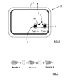
- a communication device (1) is in the form of a contactless smart card. However, it could take other forms including flush contact card, USB key or other.
- This device is intended to communicate with a terminal (2) adapted to the type of communication supported by the chip via communication signals (R).
- the signals are of the ISO 14443 type, but could be other, in particular ISO 7616 for an interface with electrical contacts.
- the device comprises at least two microcircuits or components (3, 4), in this case two integrated circuit chips. These chips are in the example mounted on modules presenting an insulating support and connection pads connected to at least a part of a communication interface. Part may include in particular a few pads of a terminal block of electrical contacts among a set of pads.
- the microcircuits or components 3, 4 are connected in parallel to at least one common part of a communication interface (5).
- This is a radiofrequency antenna 5 having turns disposed at the periphery of the edge of the card.
- Selection means (6) for one of the microcircuits equip the device. According to one characteristic of this embodiment, these selection means are able to be actuated in response to an interaction with the outside; this interaction is distinct from the communication signals used in the implementation of the applications loaded in the microcircuits.
- the interaction does not take place via the same interface as that used for the communication between the microcircuits and the terminal.
- the messages conveyed by the modulated communication signals are not used to operate a selector.
- the invention thus has the advantage of dispensing with a compatible protocol or reader or coding and decoding means for actuating a selector of components in the device.
- the selection means are manually operable by the user.
- a switch according to a schematic diagram electric. Any type of mechanical switch, electrical, contact, push, ohmic or other can be used.
- the invention may comprise more complex switches, with multi connections, bi stable switches or others including those comprising a sensor sensitive to external radiation or other activator.
- the sensor may for example be an infrared sensor, a temperature sensor of the human body by applying a finger to a suitable cell, a pressure sensor, a sensitive sensor such as those of the sensory screens, etc.
- one of the microcircuits has priority in establishing communication with respect to the other microcircuit when they are connected in parallel and in that said selection means intervene to connect or disconnect the priority microcircuit to the microcircuit. interface.
- the microcircuit (3) is of priority type with respect to the other (4) vis-à-vis the receipt of a communication from a terminal.
- it is a chip type "Mifare” type A founders such as NXP or Infineon companies etc.
- This priority management can be done in the programming of the communication in the terminal itself (in the example Type A).
- this priority can be reversed and therefore have priority over type B for chips of founders such as Infinite, ST Microelectronics, Samsung, etc. and in this case a permutation will have to be carried out between the chips type A and B of the figure 1 .
- Priority can also come from the chip-specific response time.
- the chip B can contain an application corresponding to the standard "Calypso" of "Calypso Founders Association", defining security dialogues between terminals and cards.
- the selection means here comprise a switch positioned on at least one link of the priority microcircuit to the interface, while the non-priority chip is always connected to the interface regardless of the state of the switch.
- the electrical assembly is carried out in such a way that the priority chip of type A is connected secondly with respect to the non-priority type B chip 4, the antenna connections first connecting chip 4 and then chip 3 by a chip chip bridging.
- Such an assembly above is advantageous especially in the case of a migration of old technology to a more recent because in operation, when closing the circuit, the priority chip is connected and operates at the expense of the other. .
- the circuit or assembly is made in such a way that the chip associated with the new technology comes into operation without having to switch on the switch.
- the priority chip 3 of type A represents the new migration technology
- the non-priority chip 4 of type B representing the current technology
- FIG. 2 To the figure 2 is illustrated a sequence of waking wave train or activation of transponders comprising the elements (3 or 4 and 5).
- Some of the current radio frequency terminals or readers intermittently emit two types of signals intended for at least two types A or B of a chip so as to wake them up (“wake up A” and then "wake up B”). The terminal does so because it ignores a priori what type of chip A or B, it will have to dialogue depending on whether the user holds a single chip card type A or B.
- the switch of the figure 1 is replaced by a push-type mechanical switch; it comprises a metal dome 6a which is positioned on two links coming respectively from a chip stud 3 and 4.
- the push button may include a "Belleville” type dome washer introduced into a cavity provided for this purpose.
- said selection means 16 are operable by an external signal. This may preferably come from the terminal.
- a light signal (L) is emitted by the terminal for example when a person is detected by presence detectors, a light beam (L) or other radiates in this transaction space near the terminal.
- This light signal is captured by the card presented by a user.
- the signal is picked up by a sensor 16 disposed outside the chips 3 and 4.
- This is a photodiode 16 which is busy when it picks up light, thus closing or by passing the circuit on which she is.
- the same references designate the same elements.
- This photodiode is mounted as previously on a bridging link between the two chips.
- the cell of the photodiode opens on the surface or is covered with a transparent or translucent card material.
- the terminal activates the chip 3 or 4 by radiofrequency (R) wave trains via its own-antenna interface, in particular at 13.56 MHz and carries out the planned transactions via the antenna 5 of the map.
- R radiofrequency
- the switch comprises an element sensitive to the communication signals transmitted by the terminal.
- the switch may be a radio frequency sensor and include for example a suitable antenna.
- the sensor can preferably be set to very quickly capture the radio frequency signals before or at the same time that the woken chip does not begin to communicate and do a complete transaction to the end (authentication, payment, access ).
- this sensor may comprise a flat antenna or coil of the antenna type 5 and activate a relay or a circuit breaker under the effect of a wave train such as that used for waking the chips illustrated in FIG. the figure 2 .
- the maintenance of the switch can possibly be carried out by a timer coupled to the switch and which will collect radio frequency energy and store it for example in a capacity.
- the maintenance energy of the switch can be performed in particular by the discharge of the capacity.
- the invention does not use the signals of the reader but only in this case the energy of the radio frequency waves used to convey the signals or communication messages. There is therefore no need either in this case to code or decode signals from the terminal. The invention therefore ignores the protocol used by the reader to select a microcircuit or an application
- the switch is disposed outside the chips, so as not to have to change them and for simplicity of implementation.
- an internal arrangement of the switch in one and / or other chip (s) in integrated form could also be provided by the invention.
- the advantage here is to overcome a terminal communication protocol which is useful during a migration.
- the chips are selected automatically by equipping the readers either with a radiation emitter (L) in particular light (or other such as infrared ...) and by providing the appropriate switch accordingly in the device.
- a radiation emitter L in particular light (or other such as infrared )
- the radiation activates a photodiode to cut the circuit of a priority chip or type A microcircuit belonging to a long-time technology to be replaced.
- the terminal no longer emits radiation (the latter having been deactivated) and the chip type B belonging to the new technology remains enabled by default automatically.
- the priority chip 3 type A is activated by default without radiation because its circuit is closed by default at rest without radiation, then under the effect of radiation or other activation of the switch or contactor, the circuit opens leaving thus the communication to the other non-priority chip but representing the new migration technology.
- This mode of operation has the advantage of offering more security because it must be close to the terminal to close the circuit, the user does not even have to operate himself the switch.
- the invention allows to use two or more chips of different or identical type for applications or reserved uses.
- a user may reserve a chip for small current transactions and use another chip for larger amounts.
- the chips may have different security features depending on the application.
- a chip can be used for access in a company, to pay the company restaurant, to pay in drink dispensers while the other chip is used to connect to a computer or to authenticate on a network by putting in create prerecorded passwords ...
- Another use is to reserve one chip for storage of non-sensitive data while the other implements Cipher operations and specific session keys.
- the implementation is different, especially over time.
- a user can use a chip containing sensitive data for trust transactions and another for risky transactions with an outside world, the advantage being that the chips are perfectly compartmentalized and can thus include secrets of different operators. .
- the priority chip is dedicated to large transactions and requires a voluntary operation of the user as a pressure on a push button to validate or allow a transaction including contactless.
- This chip 3 is connected as on the figure 3 while the non-priority type B chip 4 is used for transactions of a lower amount such as switching to the subway by operating as an electronic purse for small financial transactions.
- the invention therefore provides a simple way to gain flexibility in use according to the uses and / or applications at the discretion of the user with the possible additional security and control over operations with a single card.
- the microcircuit selection means 3, 4 may comprise a keypad with two or more keys for entering an access code to one or the other microcircuit.
- the invention may comprise "n" microcircuits and "n” applications, the selection means for selecting each microcircuit and / or application.
- the switch can also be an incrementing selector or switching from one microcircuit to another with each intervention of the user.
Abstract
Description
La présente invention concerne un dispositif de communication comportant deux puces reliées à une interface de communication au moins en partie commune.The present invention relates to a communication device comprising two chips connected to a communication interface at least partly common.
Elle concerne en particulier des dispositifs sans contact comportant une ou plusieurs applications logicielles. Ces applications peuvent servir notamment à des accès et/ou des paiements et/ou identifications en relation avec des terminaux radiofréquences.It relates in particular contactless devices comprising one or more software applications. These applications can be used in particular for access and / or payments and / or identifications in connection with radio frequency terminals.
Le dispositif peut être tout objet portable comportant un transpondeur radiofréquence tel qu'une carte, étiquette électronique, passeport, montre, téléphone etc. Un transpondeur comprend un microcircuit électronique relié à une interface de communication à antenne. De tels transpondeurs fonctionnent notamment selon la norme ISO 14443 mais l'invention n'est pas limitée cette norme ni au protocole de communication qui y est relatif.The device can be any portable object comprising a radio frequency transponder such as a card, electronic tag, passport, watch, phone etc. A transponder comprises an electronic microcircuit connected to an antenna communication interface. Such transponders operate in particular according to the ISO 14443 standard, but the invention is not limited to this standard nor to the communication protocol relating thereto.
La demande de brevet
La demande de brevet
L'invention a d'abord pour objectif de permettre une migration d'une technologie et/ou protocole utilisée par un couple terminaux /dispositif portables vers une nouvelle technologie de terminaux et/ou cartes associées et/ou nouveau protocole et ce à moindre coût et/ou avec des moyens simples à mettre en oeuvreThe invention aims first of all at enabling a migration of a technology and / or protocol used by a couple terminals / portable device to a new technology of terminals and / or associated cards and / or new protocol and at a lower cost and / or with simple means to implement
L'invention vise à offrir plus de souplesse d'utilisation selon les utilisations et/ou applications au gré de l'utilisateur avec le cas échéant plus de sécurité et de contrôle sur les opérations avec un seul dispositif de préférence sous forme de carte à puce.The invention aims to offer more flexibility of use depending on the uses and / or applications at the discretion of the user with the possible additional security and control operations with a single device preferably in the form of a smart card .
L'invention réside dans la fourniture d'un dispositif portable à au moins deux microcircuits aptes à contenir des applications et dans des moyens de sélection de l'un des au moins deux microcircuits qui soient distincts de moyens de décodage ou logiciel; ces moyens de sélection sont au contraire basés sur l'exploitation ou la mise en oeuvre d'une énergie : pression mécanique, force, énergie électrique, photo-électrique... ; Le cas échéant, de préférence, cette énergie ou force intervient sur des moyens disposés à l'extérieur des microcircuits, pour éviter leur modification. L'actionnement de ces moyens doit pouvoir s'effectuer, de préférence, avec le moins possible de modifications du terminal voire aucune.The invention lies in the provision of a portable device to at least two microcircuits capable of containing applications and in selection means of one of the at least two microcircuits which are distinct from decoding or software means; these selection means are instead based on the exploitation or the implementation of an energy: mechanical pressure, force, electrical energy, photoelectric ...; Where appropriate, preferably, this energy or force intervenes on means disposed outside the microcircuits, to avoid their modification. The actuation of these means must be carried out, preferably with the least possible modifications of the terminal or none.
L'invention a donc pour objet un dispositif portable de communication destiné à communiquer avec un terminal, ledit dispositif comportant au moins deux microcircuits branchés en parallèle sur au moins une partie d'une interface de communication commune, des moyens de sélection de l'un des microcircuits.The invention therefore relates to a portable communication device intended to communicate with a terminal, said device comprising at least two microcircuits connected in parallel on at least a part of a common communication interface, means for selecting one microcircuits.
Le dispositif se distingue en ce que lesdits moyens de sélection sont aptes à être actionnés par une interaction avec l'extérieur du dispositif, ladite interaction étant distincte d'une réception et/ou interprétation de signal de communication.The device is distinguished in that said selection means are able to be actuated by an interaction with the outside of the device, said interaction being distinct from a reception and / or interpretation of a communication signal.
Selon d'autres caractéristiques :
- lesdits moyens de sélection sont actionnables manuellement;
- lesdits moyens de sélection sont actionnables par un signal émis par le terminal;
- Selon une caractéristique préférée, l'un des microcircuits est prioritaire dans l'établissement de la communication par rapport à l'autre microcircuit et lesdits moyens de sélection interviennent pour connecter ou déconnecter le microcircuit prioritaire par rapport à l'interface.
- said selection means are manually operable;
- said selection means are operable by a signal transmitted by the terminal;
- According to a preferred characteristic, one of the microcircuits has priority in the establishment of the communication with respect to the other microcircuit and said selection means intervene to connect or disconnect the priority microcircuit with respect to the interface.
Cet aspect prioritaire entre les deux microcircuits est exploité avantageusement dans l'invention pour créer, d'une part un fonctionnement par défaut du dispositif (sans intervention de l'utilisateur ou de l'extérieur), et/ou d'autre part un fonctionnement nécessitant une intervention volontaire ou contrôle de l'utilisateur sur les moyens de sélection. L'intervention précitée pouvant aussi bien connecter que déconnecter le microcircuit prioritaire.
- Dans un cas, simple, les moyens de sélection comprennent un interrupteur de type à actionnement mécanique positionné sur au moins une liaison du microcircuit prioritaire à l'interface.
- Dans un autre cas, dit automatique, lesdits moyens de sélection comprennent un interrupteur à capteur; ce dernier peut être de préférence sensible à un rayonnement.
- De préférence, l'interface de communication est de type radiofréquence mais l'invention s'applique à d'autre type d'interface notamment de type à contacts électriques, capacitif, optique...
- Selon un mode de réalisation relative à une interface à contacts électriques, L'invention prévoit de préférence, d'utiliser une interaction sans-contact telle qu'un rayonnement lumineux, infrarouge, radiofréquence, capacitif ou autre avec le dispositif, ce dernier comportant des moyens de sélection sensibles à cette interaction sans contact.
- In a simple case, the selection means comprise a mechanically actuated type switch positioned on at least one link of the priority microcircuit at the interface.
- In another case, said automatic, said selection means comprise a sensor switch; the latter may be preferably sensitive to radiation.
- Preferably, the communication interface is of radiofrequency type but the invention applies to other type of interface, in particular of the type with electrical contacts, capacitive, optical ...
- According to an embodiment relating to an interface with electrical contacts, the invention preferably provides for the use of a non-contact interaction such as light, infrared, radiofrequency, capacitive or other radiation with the device, the latter comprising selection means responsive to this contactless interaction.
Grâce à de telles dispositions, l'invention permet d'utiliser des microcircuits existants sans avoir à modifier de leur circuit "hardware", intégré ou non, ou sans avoir à effectuer une programmation supplémentaire et/ou ni à disposer des moyens de codage interne dans le dispositif pour décoder un signal de terminal.Thanks to such provisions, the invention makes it possible to use existing microcircuits without having to modify their "hardware" circuit, integrated or not, or without having to carry out additional programming and / or to have internal coding means available. in the device for decoding a terminal signal.
Les moyens de sélection de l'invention interviennent sur les liaisons entre les plots entrée / sortie des microcircuits et l'interface de communication (antenne ou plages de contact électriques). Ces liaisons sont fermées ou ouvertes selon des modes de réalisation ou montages particuliers.The selection means of the invention intervene on the links between the input / output pads of the microcircuits and the communication interface (antenna or electrical contact pads). These links are closed or open according to particular embodiments or assemblies.
La fabrication du dispositif est simple puisqu'il suffit d'interposer des moyens de sélection entre les microcircuits et leur interface. Dans un mode de réalisation, il suffit d'une simple diode sensible à la lumière, placée sur une liaison d'une puce à l'interface suffit. Une "led" ou émetteur lumineux est aussi installé sur le terminal tout simplement sur un circuit d'alimentation. Le terminal peut mais n'a pas l'obligation de moduler le rayonnement pour le coder et actionner les moyens de sélection.
- Selon un autre mode de réalisation, on évite de modifier le terminal même de manière minime comme ci-dessus. Selon ce mode on utilise l'énergie modulée transmise au dispositif pour actionner les moyens de sélection. L'énergie peut être de type radiofréquence ou autre. Et côté dispositif, les moyens de sélection utilisent cette énergie pour actionner un interrupteur ou contacteur adapté à cet effet, indépendamment du message véhiculé destiné à lancer une application.
- According to another embodiment, it is avoided to modify the terminal itself in a minimal way as above. According to this mode, the modulated energy transmitted to the device is used to actuate the selection means. The energy may be radio frequency or other type. And on the device side, the selection means use this energy to actuate a switch or contactor adapted for this purpose, independently of the conveyed message intended to launch an application.
L'invention a l'avantage d'offrir également une solution au vol d'information à l'insu du porteur par des moyens radiofréquences tout en maintenant une souplesse d'utilisation pour d'autres applications (notamment lors d'une utilisation sans intervention volontaire de l'utilisateur ou sans actionnement intentionnel des moyens de sélection dans le cadre d'applications fréquentes telles que transport, prépaiement...).
- Dans un mode de réalisation dans lequel le dispositif est une carte sans contact, on dispose un interrupteur à capteur réceptif de type "Led" sensible à un rayonnement sur une liaison d'un plot de puce à un plot de l'autre puce ou sur une liaison directe à l'antenne. La carte est ensuite laminée avec une feuille transparente ou translucide ou une feuille comportant une fenêtre sur l'extérieur.
- In one embodiment in which the device is a contactless card, there is a radiation-sensitive "Led" type receptive sensor switch on a link from one chip pad to a pad of the other chip or on a direct connection to the antenna. The card is then laminated with a transparent or translucent sheet or a sheet having a window on the outside.
Un autre avantage de l'invention est de permettre une sélection d'une puce correspondant à l'application souhaitée sur un même support, de manière simple, sans modifier les microcircuits et/ou le codage ou instructions des terminaux.Another advantage of the invention is to allow a selection of a chip corresponding to the desired application on the same medium, in a simple manner, without modifying the microcircuits and / or the coding or instructions of the terminals.
De cette manière la migration est facilitée pour un utilisateur puisqu'il a toujours un seul et même support. Ce support peut comprendre les deux microcircuits noyés dans un corps tel un corps de carte à puce.In this way the migration is facilitated for a user since he always has one and the same support. This support may comprise the two microcircuits embedded in a body such as a smart card body.
D'autres caractéristiques et avantages de l'invention ressortiront de la description qui suit, faite à titre illustratif et nullement limitatif, en se référant aux dessins ci-annexés sur lesquels
- la
figure 1 illustre un premier mode de réalisation du dispositif conforme à l'invention; - la
figure 2 illustre des signaux de communications émis par un terminal à destination du dispositif selon un mode de réalisation; - la
figure 3 illustre un deuxième mode particulier de réalisation du dispositif conforme à l'invention; - la
figure 4 illustre un troisième mode de réalisation du dispositif conforme à l'invention.
- the
figure 1 illustrates a first embodiment of the device according to the invention; - the
figure 2 illustrates communications signals transmitted by a terminal to the device according to one embodiment; - the
figure 3 illustrates a second particular embodiment of the device according to the invention; - the
figure 4 illustrates a third embodiment of the device according to the invention.
A la
Le dispositif comporte au moins deux microcircuits ou composants (3, 4), en l'occurrence deux puces de circuits intégrés. Ces puces sont dans l'exemple montées sur des modules présentant un support isolant et des plages de connexion reliées à au moins une partie d'une interface de communication. Une partie peut comprendre notamment quelques plots d'un bornier de contacts électriques parmi un ensemble de plots.The device comprises at least two microcircuits or components (3, 4), in this case two integrated circuit chips. These chips are in the example mounted on modules presenting an insulating support and connection pads connected to at least a part of a communication interface. Part may include in particular a few pads of a terminal block of electrical contacts among a set of pads.
Les microcircuits ou composants 3, 4 sont branchés en parallèle sur au moins une partie commune d'une interface de communication (5). Il s'agit ici d'une antenne radiofréquence 5 comportant des spires disposées en périphérie du bord de la carte.The microcircuits or
Des moyens de sélection (6) de l'un des microcircuits équipent le dispositif. Selon une caractéristique de ce mode de réalisation, ces moyens de sélection sont aptes à être actionnés en réponse à une interaction avec l'extérieur; cette interaction est distincte des signaux de communication utilisés dans la mise en oeuvre des applications chargés dans les microcircuits.Selection means (6) for one of the microcircuits equip the device. According to one characteristic of this embodiment, these selection means are able to be actuated in response to an interaction with the outside; this interaction is distinct from the communication signals used in the implementation of the applications loaded in the microcircuits.
En d'autres termes, dans cet exemple, l'interaction ne s'effectue pas via la même interface que celle utilisée pour la communication entre les microcircuits et le terminal. Ou encore, les messages véhiculés par les signaux de communication modulés ne servent pas à actionner un sélecteur.In other words, in this example, the interaction does not take place via the same interface as that used for the communication between the microcircuits and the terminal. Or, the messages conveyed by the modulated communication signals are not used to operate a selector.
L'invention a l'avantage ainsi de s'affranchir de protocole ou lecteur compatible ou moyens de codage et décodage pour actionner un sélecteur de composants dans le dispositif.The invention thus has the advantage of dispensing with a compatible protocol or reader or coding and decoding means for actuating a selector of components in the device.
Dans ce premier mode de réalisation, les moyens de sélection sont actionnables manuellement par l'utilisateur. Dans le premier mode, est illustré un interrupteur selon un schéma de principe électrique. Tout type d'interrupteur mécanique, électrique, à contact, poussoir, ohmique ou autre peut être utilisé.In this first embodiment, the selection means are manually operable by the user. In the first mode, is illustrated a switch according to a schematic diagram electric. Any type of mechanical switch, electrical, contact, push, ohmic or other can be used.
L'invention peut comprendre des interrupteurs plus complexes, à multi connexions, des interrupteurs bi stables ou autres notamment ceux comprenant un capteur sensible à un rayonnement externe ou autre activateur.The invention may comprise more complex switches, with multi connections, bi stable switches or others including those comprising a sensor sensitive to external radiation or other activator.
Le capteur peut être par exemple un capteur infrarouge, un capteur de température du corps humain par application d'un doigt sur une cellule adaptée, un capteur de pression, un capteur sensitif comme ceux des écrans sensitifs, etc.The sensor may for example be an infrared sensor, a temperature sensor of the human body by applying a finger to a suitable cell, a pressure sensor, a sensitive sensor such as those of the sensory screens, etc.
Selon une caractéristique, l'un des microcircuits est prioritaire dans l'établissement de la communication par rapport à l'autre microcircuit quand ils sont connectés en parallèle et en ce que lesdits moyens de sélection interviennent pour connecter ou déconnecter le microcircuit prioritaire à l'interface.According to one characteristic, one of the microcircuits has priority in establishing communication with respect to the other microcircuit when they are connected in parallel and in that said selection means intervene to connect or disconnect the priority microcircuit to the microcircuit. interface.
Dans l'exemple, le microcircuit (3) est de type prioritaire par rapport à l'autre (4) vis à vis de la réception d'une communication provenant d'un terminal. En particulier, il s'agit d'une puce de type "Mifare" de type A des fondeurs tels que les sociétés NXP ou Infineon etc. Cette gestion de priorité peut être faite dans la programmation de la communication dans le Terminal même (dans l'exemple Type A). Cependant cette priorité peut être donc inversée et donc avoir une priorité sur le type B pour les puces des fondeurs tels qu'lnfinéon, ST Microelectronics, Samsung, etc. et dans ce cas une permutation devra être effectuée entre les puces type A et B de la
Les moyens de sélection comprennent ici un interrupteur positionné sur au moins une liaison du microcircuit prioritaire à l'interface, alors que la puce non prioritaire est toujours connectée à l'interface quel que soit l'état de l'interrupteur.The selection means here comprise a switch positioned on at least one link of the priority microcircuit to the interface, while the non-priority chip is always connected to the interface regardless of the state of the switch.
De manière avantageuse, le montage électrique est réalisé de telle sorte que la puce prioritaire de type A se trouve connectée en second lieu par rapport à la puce 4 non prioritaire de type B, les connexions d'antenne connectant d'abord la puce 4 puis la puce 3 par un pontage de puce à puce.Advantageously, the electrical assembly is carried out in such a way that the priority chip of type A is connected secondly with respect to the non-priority
Un tel montage ci-dessus est avantageux notamment dans le cas d'une migration de technologie ancienne vers une plus récente car en fonctionnement, lorsqu'on ferme le circuit, la puce prioritaire est connectée et se met en fonctionnement au détriment de l'autre. On réalise le circuit ou montage de manière que la puce associée à la nouvelle technologie se mette en fonctionnement sans avoir à terme à actionner l'interrupteur.Such an assembly above is advantageous especially in the case of a migration of old technology to a more recent because in operation, when closing the circuit, the priority chip is connected and operates at the expense of the other. . The circuit or assembly is made in such a way that the chip associated with the new technology comes into operation without having to switch on the switch.
Par exemple, si la puce prioritaire 3 de type A représente la nouvelle technologie de migration, il convient préférentiellement de faire un circuit de manière que cette puce soit connectée à l'antenne quand l'interrupteur est au repos. Autrement dit, pour le fonctionnement de la puce non prioritaire 4 de type B, représentant la technologie courante, il faudra actionner l'interrupteur jusqu'à la migration, ce qui en général représente une période plus courte que la période d'usage de la nouvelle technologie de type A.For example, if the
A la
A la
A la
Ce signal lumineux est capté par la carte présentée par un utilisateur. De préférence, le signal est capté par un capteur 16 disposé à l'extérieur des puces 3 et 4. Il s'agit ici d'une photodiode 16 qui est passante quand elle capte de la lumière, fermant ainsi ou en rendant passant le circuit sur lequel elle se trouve. Dans cette
Cette photodiode est montée comme précédemment sur une liaison de pontage entre les deux puces. La cellule de la photodiode débouche en surface ou est recouverte d'un matériau de la carte transparent ou translucide. Parallèlement ou ensuite, le terminal active la puce 3 ou 4 par des trains d'onde radiofréquences (R) par son interface à antenne propre, notamment à 13,56 MHz et effectue les transactions prévues par le biais de l'antenne 5 de la carte.This photodiode is mounted as previously on a bridging link between the two chips. The cell of the photodiode opens on the surface or is covered with a transparent or translucent card material. In parallel or later, the terminal activates the
Dans un autre mode de réalisation (non représenté) l'interrupteur comprend un élément sensible aux signaux de communication émis par le terminal. L'interrupteur peut être un capteur de type radiofréquence et comprendre par exemple une antenne adaptée.In another embodiment (not shown) the switch comprises an element sensitive to the communication signals transmitted by the terminal. The switch may be a radio frequency sensor and include for example a suitable antenna.
Le capteur peut être de préférence réglé pour capter très rapidement les signaux radiofréquences avant même ou en même temps que la puce réveillée ne se mette à communiquer et ne réaliser une transaction complète jusqu'au bout (authentification, paiement, accès...).The sensor can preferably be set to very quickly capture the radio frequency signals before or at the same time that the woken chip does not begin to communicate and do a complete transaction to the end (authentication, payment, access ...).
Ainsi par exemple, ce capteur peut comprendre une antenne plate ou bobine du type de l'antenne 5 et activer un relais ou un coupe circuit sous l'effet d'un train d'onde tel que celui utilisé pour le réveil des puces illustré à la
Le maintien de l'interrupteur peut éventuellement s'effectuer par un temporisateur couplé à l'interrupteur et qui va recueillir l'énergie radiofréquence et la stocker par exemple dans une capacité. L'énergie de maintien de l'interrupteur peut s'effectuer notamment par la décharge de la capacité.The maintenance of the switch can possibly be carried out by a timer coupled to the switch and which will collect radio frequency energy and store it for example in a capacity. The maintenance energy of the switch can be performed in particular by the discharge of the capacity.
On remarque que l'invention n'utilise pas les signaux du lecteur mais uniquement dans ce cas l'énergie des ondes radiofréquences utilisées pour véhiculer les signaux ou messages de communication. Il n'y a donc pas de nécessité non plus dans ce cas de coder ou décoder des signaux provenant du terminal. L'invention fait donc abstraction du protocole utilisé par le lecteur pour sélectionner un microcircuit ou une applicationNote that the invention does not use the signals of the reader but only in this case the energy of the radio frequency waves used to convey the signals or communication messages. There is therefore no need either in this case to code or decode signals from the terminal. The invention therefore ignores the protocol used by the reader to select a microcircuit or an application
De préférence, l'interrupteur est disposé à l'extérieur des puces, de manière à ne pas avoir à les modifier et pour la simplicité de mise en oeuvre. Toutefois, une disposition interne de l'interrupteur dans l'une et/ou autre puce(s) sous forme intégrée pourrait être également prévue par l'invention. L'avantage ici est de s'affranchir d'un protocole de communication des terminaux ce qui est utile lors d'une migration.Preferably, the switch is disposed outside the chips, so as not to have to change them and for simplicity of implementation. However, an internal arrangement of the switch in one and / or other chip (s) in integrated form could also be provided by the invention. The advantage here is to overcome a terminal communication protocol which is useful during a migration.
Il n'y a donc pas besoin de coder ou décoder les signaux via une couche logicielle ou hardware dans la puce. L'invention se concentre dans cet exemple sur l'énergie des signaux.There is therefore no need to code or decode the signals via a software or hardware layer in the chip. The invention concentrates in this example on the energy of the signals.
La sélection des puces s'effectue automatiquement en équipant les lecteurs soit d'un émetteur de rayonnement (L) notamment lumineux (ou autre tel que infrarouge...) et en prévoyant l'interrupteur adapté en conséquence dans le dispositif.The chips are selected automatically by equipping the readers either with a radiation emitter (L) in particular light (or other such as infrared ...) and by providing the appropriate switch accordingly in the device.
Selon un autre mode d'utilisation, avant une migration, le rayonnement actionne une photodiode pour couper le circuit d'une puce prioritaire ou microcircuit de type A appartenant à une technologie révolue à remplacer. Après la migration, le terminal n'émet plus de rayonnement (celui-ci ayant été désactivé) et la puce de type B appartenant à la nouvelle technologie reste activée par défaut de manière automatique.According to another mode of use, before a migration, the radiation activates a photodiode to cut the circuit of a priority chip or type A microcircuit belonging to a long-time technology to be replaced. After the migration, the terminal no longer emits radiation (the latter having been deactivated) and the chip type B belonging to the new technology remains enabled by default automatically.
Inversement, la puce prioritaire 3 de type A est activée par défaut sans rayonnement car son circuit est fermé par défaut au repos sans rayonnement, puis sous l'effet du rayonnement ou autre activation de l'interrupteur ou contacteur, le circuit s'ouvre laissant ainsi la communication à l'autre puce non prioritaire mais représentant la nouvelle technologie de migration.Conversely, the
Ce mode de fonctionnement a l'avantage d'offrir plus de sécurité car il faut être proche du terminal pour fermer le circuit, l'utilisateur n'ayant même pas à actionner lui même l'interrupteur.This mode of operation has the advantage of offering more security because it must be close to the terminal to close the circuit, the user does not even have to operate himself the switch.
On remarque aussi selon un mode de mise en oeuvre que l'invention permet d'utiliser deux ou plusieurs puces de type différents ou identiques destinées à des applications ou usages réservés.Note also according to an embodiment that the invention allows to use two or more chips of different or identical type for applications or reserved uses.
Un utilisateur peut par exemple réserver une puce à des transactions courantes de faible montant et utiliser une autre puce pour des montants plus importants. Les puces peuvent présenter des caractéristiques de sécurité différentes selon l'application.For example, a user may reserve a chip for small current transactions and use another chip for larger amounts. The chips may have different security features depending on the application.
Une puce peut servir à des accès dans une entreprise, à payer le restaurant d'entreprise, à payer dans des distributeurs de boissons tandis que l'autre puce est utilisée pour se connecter à un ordinateur ou s'authentifier sur un réseau en mettant en oeuvre des mots de passe préenregistrés...A chip can be used for access in a company, to pay the company restaurant, to pay in drink dispensers while the other chip is used to connect to a computer or to authenticate on a network by putting in create prerecorded passwords ...
Une autre utilisation est de réserver une puce pour le stockage de données non sensibles tandis que l'autre met en oeuvre des opérations de chiffrements et clés de session spécifiques. La mise en oeuvre est donc différente, notamment au fil du temps.Another use is to reserve one chip for storage of non-sensitive data while the other implements Cipher operations and specific session keys. The implementation is different, especially over time.
Un utilisateur peut utiliser une puce contenant des données sensibles pour des transactions de confiances et une autre pour des transactions à risques avec un monde extérieur, l'avantage étant que les puces sont parfaitement cloisonnées et peuvent comprendre de ce fait des secrets d'opérateurs différents.A user can use a chip containing sensitive data for trust transactions and another for risky transactions with an outside world, the advantage being that the chips are perfectly compartmentalized and can thus include secrets of different operators. .
Dans un autre exemple, la puce prioritaire est consacrée à des transactions importantes et requiert un actionnement volontaire de l'utilisateur comme une pression sur un bouton poussoir pour valider ou permettre une transaction notamment sans contact.In another example, the priority chip is dedicated to large transactions and requires a voluntary operation of the user as a pressure on a push button to validate or allow a transaction including contactless.
Cette puce 3 est branchée comme sur la
On voit bien que le dispositif est utilisé sans même l'actionner ou le sortir d'un sac (pour le métro), tandis que pour des transactions importantes nécessitant un contrôle de l'utilisateur, il faut actionner l'interrupteur fermant le circuit et activant la puce prioritaire.It is clear that the device is used without even actuating it or taking it out of a bag (for the metro), whereas for major transactions requiring user control, it is necessary to actuate the switch closing the circuit and activating the priority chip.
L'invention offre donc un moyen simple de gagner en souplesse d'utilisation selon les utilisations et/ou applications au gré de l'utilisateur avec le cas échéant plus de sécurité et de contrôle sur les opérations avec une seule carte.The invention therefore provides a simple way to gain flexibility in use according to the uses and / or applications at the discretion of the user with the possible additional security and control over operations with a single card.
Dans une variante (non représentée), les moyens de sélection des microcircuits 3, 4, peuvent comprendre un clavier à deux ou plusieurs touches pour la saisie d'un code d'accès à l'une ou l'autre microcircuit. L'invention peut comprendre "n" microcircuits et "n" applications, les moyens de sélection permettant de sélectionner chaque microcircuit et/ou application. L'interrupteur peut être aussi un sélecteur incrémentant ou passant d'un microcircuit à l'autre à chaque intervention de l'utilisateur.In a variant (not shown), the microcircuit selection means 3, 4 may comprise a keypad with two or more keys for entering an access code to one or the other microcircuit. The invention may comprise "n" microcircuits and "n" applications, the selection means for selecting each microcircuit and / or application. The switch can also be an incrementing selector or switching from one microcircuit to another with each intervention of the user.
Claims (7)
caractérisé en ce que lesdits moyens de sélection (6, 6a, 16) sont aptes à être actionnés par une interaction avec l'extérieur du dispositif, ladite interaction étant distincte d'une réception et/ou interruption de signal de communication.Communication device for communicating with a terminal, said device comprising at least two microcircuits (3, 4) connected in parallel to at least a part of a common communication interface and means for selecting one of the microcircuits,
characterized in that said selection means (6, 6a, 16) are operable by an interaction with the outside of the device, said interaction being distinct from a reception and / or interruption of a communication signal.
Priority Applications (4)
| Application Number | Priority Date | Filing Date | Title |
|---|---|---|---|
| EP09305326A EP2242005A1 (en) | 2009-04-16 | 2009-04-16 | Communication device comprising two chips with common communication interface |
| EP10711673.3A EP2419865B1 (en) | 2009-04-16 | 2010-03-29 | Communication device comprising two chips with common communication interface |
| ES10711673.3T ES2538397T3 (en) | 2009-04-16 | 2010-03-29 | Communication device that includes two chips with a common communication interface |
| PCT/EP2010/054119 WO2010118947A1 (en) | 2009-04-16 | 2010-03-29 | Communication device comprising two chips with a shared communication interface |
Applications Claiming Priority (1)
| Application Number | Priority Date | Filing Date | Title |
|---|---|---|---|
| EP09305326A EP2242005A1 (en) | 2009-04-16 | 2009-04-16 | Communication device comprising two chips with common communication interface |
Publications (1)
| Publication Number | Publication Date |
|---|---|
| EP2242005A1 true EP2242005A1 (en) | 2010-10-20 |
Family
ID=40941812
Family Applications (2)
| Application Number | Title | Priority Date | Filing Date |
|---|---|---|---|
| EP09305326A Withdrawn EP2242005A1 (en) | 2009-04-16 | 2009-04-16 | Communication device comprising two chips with common communication interface |
| EP10711673.3A Active EP2419865B1 (en) | 2009-04-16 | 2010-03-29 | Communication device comprising two chips with common communication interface |
Family Applications After (1)
| Application Number | Title | Priority Date | Filing Date |
|---|---|---|---|
| EP10711673.3A Active EP2419865B1 (en) | 2009-04-16 | 2010-03-29 | Communication device comprising two chips with common communication interface |
Country Status (3)
| Country | Link |
|---|---|
| EP (2) | EP2242005A1 (en) |
| ES (1) | ES2538397T3 (en) |
| WO (1) | WO2010118947A1 (en) |
Cited By (1)
| Publication number | Priority date | Publication date | Assignee | Title |
|---|---|---|---|---|
| FR2968803A1 (en) * | 2010-12-10 | 2012-06-15 | St Microelectronics Rousset | Electromagnetic transponder e.g. dual integrated circuit card, for contactless exchanging of protected data with reader for bank card, has electric circuit switched from one state to another state when resonant circuit is powered by reader |
Families Citing this family (2)
| Publication number | Priority date | Publication date | Assignee | Title |
|---|---|---|---|---|
| CN102468988A (en) * | 2010-11-11 | 2012-05-23 | 上海华虹集成电路有限责任公司 | Device for automatically detecting signal protocol type in international standardization organization/international electrotechnical commission (ISO/IEC) 14443 protocol |
| GB201506954D0 (en) * | 2015-04-23 | 2015-06-10 | Royal College Of Art | Communications device system and method |
Citations (4)
| Publication number | Priority date | Publication date | Assignee | Title |
|---|---|---|---|---|
| FR2680262A1 (en) | 1991-08-08 | 1993-02-12 | Gemplus Card Int | Integrated circuits for chip card and multichip card using these circuits |
| EP0779598A2 (en) * | 1995-12-14 | 1997-06-18 | Hitachi, Ltd. | Multichip IC card and IC card system using it |
| EP1267303A1 (en) | 2001-06-11 | 2002-12-18 | cubit electronics Gmbh | Transponder |
| US20070194926A1 (en) * | 1999-05-06 | 2007-08-23 | Bayley Oliver T | Interactive radio frequency tags |
Family Cites Families (1)
| Publication number | Priority date | Publication date | Assignee | Title |
|---|---|---|---|---|
| FR2637710A1 (en) * | 1988-10-07 | 1990-04-13 | B Et Dev | Method and device for high-security multifunction electronic control comprising a microchip card |
-
2009
- 2009-04-16 EP EP09305326A patent/EP2242005A1/en not_active Withdrawn
-
2010
- 2010-03-29 WO PCT/EP2010/054119 patent/WO2010118947A1/en active Application Filing
- 2010-03-29 ES ES10711673.3T patent/ES2538397T3/en active Active
- 2010-03-29 EP EP10711673.3A patent/EP2419865B1/en active Active
Patent Citations (4)
| Publication number | Priority date | Publication date | Assignee | Title |
|---|---|---|---|---|
| FR2680262A1 (en) | 1991-08-08 | 1993-02-12 | Gemplus Card Int | Integrated circuits for chip card and multichip card using these circuits |
| EP0779598A2 (en) * | 1995-12-14 | 1997-06-18 | Hitachi, Ltd. | Multichip IC card and IC card system using it |
| US20070194926A1 (en) * | 1999-05-06 | 2007-08-23 | Bayley Oliver T | Interactive radio frequency tags |
| EP1267303A1 (en) | 2001-06-11 | 2002-12-18 | cubit electronics Gmbh | Transponder |
Cited By (1)
| Publication number | Priority date | Publication date | Assignee | Title |
|---|---|---|---|---|
| FR2968803A1 (en) * | 2010-12-10 | 2012-06-15 | St Microelectronics Rousset | Electromagnetic transponder e.g. dual integrated circuit card, for contactless exchanging of protected data with reader for bank card, has electric circuit switched from one state to another state when resonant circuit is powered by reader |
Also Published As
| Publication number | Publication date |
|---|---|
| ES2538397T3 (en) | 2015-06-19 |
| EP2419865B1 (en) | 2014-11-26 |
| WO2010118947A1 (en) | 2010-10-21 |
| EP2419865A1 (en) | 2012-02-22 |
Similar Documents
| Publication | Publication Date | Title |
|---|---|---|
| EP2172877B1 (en) | Electronic device and contactless communications management contributing to such a device and a host equipment | |
| EP2507747B1 (en) | Activation and indication of an rf field on a device including a chip | |
| EP2220597B1 (en) | System with dual integrated circuit and use of said system for implementing a remote application | |
| EP2612447B1 (en) | Securing of a telecommunication device including a near-field communication module | |
| EP2194491B1 (en) | Electronic card with control means | |
| EP0670556A1 (en) | Portable device for functional link between an IC card and a central unit | |
| EP2218040A1 (en) | Radiofrequency communication device including a timer | |
| EP1116158B1 (en) | Smart card reader | |
| EP2131313A1 (en) | Method for selecting an application in a mobile wireless communication device in an NFC system and corresponding mobile wireless communication device | |
| FR2892212A1 (en) | NFC READER HAVING PASSIVE OPERATING MODE WITH LOW POWER CONSUMPTION | |
| FR2923634A1 (en) | MICROPROCESSOR CARD, TELEPHONE COMPRISING SUCH CARD, AND METHOD OF PERFORMING AN ORDER IN SUCH A CARD. | |
| EP1496470A1 (en) | Dual-mode chip card | |
| EP2419865B1 (en) | Communication device comprising two chips with common communication interface | |
| EP2065859A2 (en) | Microprocessor card, telephone comprising such a card and processing method on such a card | |
| EP2577574B1 (en) | Bank card with display screen | |
| EP2553633B1 (en) | Double-range radio frequency communication object and method for implementing same | |
| EP3012980B1 (en) | Method for managing the operation, in particular the load modulation, of an object able to contactless communicate with a reader, and corresponding device and object | |
| EP3110190B1 (en) | Method and device for managing contactless applications | |
| EP2889809A1 (en) | Device for converting an electromagnetic field | |
| EP0639486B1 (en) | Alarm system for a mobile radio station | |
| EP2251818B1 (en) | Electronic entity capable of operating in reader mode, associated chip card and method | |
| FR2770315A1 (en) | Contact-less terminal and smart card with processor and memory chip | |
| EP0870279B1 (en) | Portable device for access to at least one service provided by a server | |
| EP2401706B1 (en) | Portable device, in particular a usb flash drive, provided with several selectable contactless communication interfaces | |
| CH700045A2 (en) | Electronic card e.g. bank card, has control unit constituted of electrodes for defining screen with touch pads, where each pad is activated by finger or pen placed on contact surface opposite to pad for introducing data or command |
Legal Events
| Date | Code | Title | Description |
|---|---|---|---|
| PUAI | Public reference made under article 153(3) epc to a published international application that has entered the european phase |
Free format text: ORIGINAL CODE: 0009012 |
|
| AK | Designated contracting states |
Kind code of ref document: A1 Designated state(s): AT BE BG CH CY CZ DE DK EE ES FI FR GB GR HR HU IE IS IT LI LT LU LV MC MK MT NL NO PL PT RO SE SI SK TR |
|
| AX | Request for extension of the european patent |
Extension state: AL BA RS |
|
| STAA | Information on the status of an ep patent application or granted ep patent |
Free format text: STATUS: THE APPLICATION IS DEEMED TO BE WITHDRAWN |
|
| 18D | Application deemed to be withdrawn |
Effective date: 20110421 |