EP2224275A1 - Interference light modulator and display apparatus employing the same - Google Patents
Interference light modulator and display apparatus employing the same Download PDFInfo
- Publication number
- EP2224275A1 EP2224275A1 EP10001127A EP10001127A EP2224275A1 EP 2224275 A1 EP2224275 A1 EP 2224275A1 EP 10001127 A EP10001127 A EP 10001127A EP 10001127 A EP10001127 A EP 10001127A EP 2224275 A1 EP2224275 A1 EP 2224275A1
- Authority
- EP
- European Patent Office
- Prior art keywords
- thin film
- display apparatus
- layer
- dielectric
- light modulator
- Prior art date
- Legal status (The legal status is an assumption and is not a legal conclusion. Google has not performed a legal analysis and makes no representation as to the accuracy of the status listed.)
- Withdrawn
Links
- 229910052751 metal Inorganic materials 0.000 claims abstract description 61
- 239000002184 metal Substances 0.000 claims abstract description 61
- 125000006850 spacer group Chemical group 0.000 claims description 36
- 239000000758 substrate Substances 0.000 claims description 27
- VYPSYNLAJGMNEJ-UHFFFAOYSA-N Silicium dioxide Chemical compound O=[Si]=O VYPSYNLAJGMNEJ-UHFFFAOYSA-N 0.000 claims description 20
- 229910052681 coesite Inorganic materials 0.000 claims description 10
- 229910052906 cristobalite Inorganic materials 0.000 claims description 10
- 239000000377 silicon dioxide Substances 0.000 claims description 10
- 229910052682 stishovite Inorganic materials 0.000 claims description 10
- 229910052905 tridymite Inorganic materials 0.000 claims description 10
- 150000004767 nitrides Chemical class 0.000 claims description 7
- 229910052804 chromium Inorganic materials 0.000 claims description 4
- 229910052802 copper Inorganic materials 0.000 claims description 4
- 239000011521 glass Substances 0.000 claims description 4
- 229910052737 gold Inorganic materials 0.000 claims description 4
- 229910052750 molybdenum Inorganic materials 0.000 claims description 4
- 229910052759 nickel Inorganic materials 0.000 claims description 4
- 229910052709 silver Inorganic materials 0.000 claims description 4
- 229910052721 tungsten Inorganic materials 0.000 claims description 4
- 239000000956 alloy Substances 0.000 claims description 3
- 229910045601 alloy Inorganic materials 0.000 claims description 3
- 229910052782 aluminium Inorganic materials 0.000 claims description 2
- 239000010409 thin film Substances 0.000 abstract description 121
- 230000003287 optical effect Effects 0.000 abstract description 15
- 239000003086 colorant Substances 0.000 abstract description 7
- 239000010410 layer Substances 0.000 description 49
- 238000002310 reflectometry Methods 0.000 description 27
- 238000010521 absorption reaction Methods 0.000 description 16
- 238000001228 spectrum Methods 0.000 description 14
- GWEVSGVZZGPLCZ-UHFFFAOYSA-N Titan oxide Chemical compound O=[Ti]=O GWEVSGVZZGPLCZ-UHFFFAOYSA-N 0.000 description 6
- 239000004973 liquid crystal related substance Substances 0.000 description 6
- 239000010408 film Substances 0.000 description 3
- 238000004519 manufacturing process Methods 0.000 description 3
- 229920002120 photoresistant polymer Polymers 0.000 description 3
- 230000010287 polarization Effects 0.000 description 3
- XKRFYHLGVUSROY-UHFFFAOYSA-N Argon Chemical compound [Ar] XKRFYHLGVUSROY-UHFFFAOYSA-N 0.000 description 2
- 238000010586 diagram Methods 0.000 description 2
- 238000009792 diffusion process Methods 0.000 description 2
- 239000007769 metal material Substances 0.000 description 2
- 239000000203 mixture Substances 0.000 description 2
- 238000012986 modification Methods 0.000 description 2
- 230000004048 modification Effects 0.000 description 2
- 230000003595 spectral effect Effects 0.000 description 2
- XAGFODPZIPBFFR-UHFFFAOYSA-N aluminium Chemical compound [Al] XAGFODPZIPBFFR-UHFFFAOYSA-N 0.000 description 1
- 229910052786 argon Inorganic materials 0.000 description 1
- 238000004891 communication Methods 0.000 description 1
- 238000010276 construction Methods 0.000 description 1
- 230000007423 decrease Effects 0.000 description 1
- 230000001066 destructive effect Effects 0.000 description 1
- 239000003989 dielectric material Substances 0.000 description 1
- 238000005530 etching Methods 0.000 description 1
- 238000001914 filtration Methods 0.000 description 1
- AMGQUBHHOARCQH-UHFFFAOYSA-N indium;oxotin Chemical compound [In].[Sn]=O AMGQUBHHOARCQH-UHFFFAOYSA-N 0.000 description 1
- 239000000463 material Substances 0.000 description 1
- 238000000034 method Methods 0.000 description 1
- 238000004377 microelectronic Methods 0.000 description 1
- 238000000059 patterning Methods 0.000 description 1
- 239000011241 protective layer Substances 0.000 description 1
- 238000001039 wet etching Methods 0.000 description 1
Images


Classifications
-
- G—PHYSICS
- G02—OPTICS
- G02B—OPTICAL ELEMENTS, SYSTEMS OR APPARATUS
- G02B26/00—Optical devices or arrangements for the control of light using movable or deformable optical elements
- G02B26/001—Optical devices or arrangements for the control of light using movable or deformable optical elements based on interference in an adjustable optical cavity
Definitions
- Exemplary embodiments of the present invention relate to an interference light modulator and a display apparatus employing the same.
- Portable terminals have been developed with advanced communication and display devices. Examples of portable terminals include personal digital assistants (PDAs), portable multimedia players (PMPs), and digital multimedia broadcasting (DMB) devices.
- PDAs personal digital assistants
- PMPs portable multimedia players
- DMB digital multimedia broadcasting
- Portable terminals have largely used liquid crystal displays (LCDs) as flat display devices thereof.
- LCDs liquid crystal displays
- a LCD may include an optical switch by using the birefringence of a liquid crystal, and may realize colors by using a color filter.
- the light use efficiency of the LCD may be low.
- due to a color filter used in the LCD the light use efficiency of the LCD may be lower. Since the color filter is expensive, the LCD may also be expensive. Accordingly, there is a demand for a method of creating a color image without a color filter.
- Exemplary embodiments of the present invention relate to an interference optical modulator having excellent light use efficiency.
- Exemplary embodiments of the present invention relate to a display apparatus having excellent light use efficiency and color purity.
- Exemplary embodiments of the present invention disclose an interference light modulator comprising a substrate, a dielectric multiple thin film, a metal thin film, and a spacer.
- the dielectric multiple thin film is disposed on a surface of the substrate.
- the metal thin film is spaced apart from the dielectric multiple thin film.
- the spacer supports the dielectric multiple thin film and the metal thin film to maintain an interval between the dielectric multiple thin film and the metal thin film.
- Exemplary embodiments of the present invention disclose a display apparatus comprising a substrate, a dielectric multiple thin film, a metal thin film, a spacer, and a backlight unit.
- the dielectric multiple thin film is disposed on a surface of the substrate.
- the metal thin film is spaced apart from the dielectric multiple thin film.
- the spacer supports the dielectric multiple thin film and the metal thin film to maintain an interval between the dielectric multiple thin film and the metal thin film.
- the backlight unit emits light towards the substrate or the metal thin film.
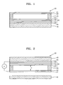
- FIG. 1 is a cross-sectional view of a light modulator according to exemplary embodiments of the present invention.
- FIG. 2 is a cross-sectional view of a display apparatus according to exemplary embodiments of the present invention.
- FIG. 3 is a cross-sectional view of a light modulator according to exemplary embodiments of the present invention.
- FIG. 4 is a diagram for explaining reflectivity and transmissivity with respect to an interval between two thin films according to exemplary embodiments of the present invention.
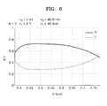
- FIG. 5 is a graph showing transmissivity with respect to wavelength when the reflectivity of each thin film of FIG. 4 is 0.7, and an interval between thin films is 700 nm according to exemplary embodiments of the present invention.
- FIG. 6 is a graph showing transmissivity and reflectivity of a dielectric multiple thin film of a display apparatus with respect to a wavelength according to exemplary embodiments of the present invention.
- FIG. 7 is a graph showing reflectivity, transmissivity, and absorption of a metal thin film of a display apparatus with respect to a wavelength according to exemplary embodiments of the present invention.
- FIG. 8A is a graph showing reflectivity, transmissivity, and absorption with respect to wavelength when a spacer of a display apparatus has a height of 200 nm according to exemplary embodiments of the present invention.
- FIG. 8B is a graph showing a spectrum of light transmitted through a light modulator of a display apparatus when a spacer has a height of 200 nm according to exemplary embodiments of the present invention.
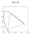
- FIG. 8C shows color gamut when a spacer has a height of 200 nm according to exemplary embodiments of the present invention.
- FIG. 9A is a graph showing reflectivity, transmissivity, and absorption with respect to wavelength when a spacer of a display apparatus has a height of 200 nm according to exemplary embodiments of the present invention.
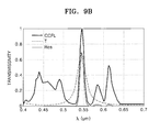
- FIG. 9B is a graph showing a spectrum of light transmitted through a light modulator of a display apparatus when a spacer has a height of 140 nm according to exemplary embodiments of the present invention.
- FIG. 9C shows color gamut when a spacer of a display apparatus has a height of 140 nm according to exemplary embodiments of the present invention.
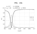
- FIG. 10A is a graph showing reflectivity, transmissivity, and absorption with respect to wavelength when a spacer of a display apparatus has a height of 64 nm according to exemplary embodiments of the present invention.
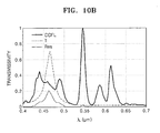
- FIG. 10B is a graph showing a spectrum of light transmitted through a light modulator of a display apparatus when a spacer has a height of 64 nm according to exemplary embodiments of the present invention.
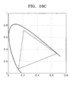
- FIG. 10C shows color gamut when a spacer of a display apparatus has a height of 64 nm according to exemplary embodiments of the present invention.
- FIG. 1 shows color gamut in a display apparatus according to exemplary embodiments of the present invention.
- FIG. 12 is a diagram showing a black mode of a display apparatus according to exemplary embodiments of the present invention.
- FIG. 13A is a graph showing transmissivity, reflectivity, and absorption in a black mode of a display apparatus according to exemplary embodiments of the present invention.
- FIG. 13B is a graph showing a spectrum in a black mode of a display apparatus according to exemplary embodiments of the present invention.
- a display apparatus may realize colors by using the interference of light, may embody a switching operation, and may include a micro electronic mechanical system (MEMS) structure.
- the display apparatus may not include any color filter to realize colors.
- FIG. 1 is a cross-sectional view of a light modulator 20 according to exemplary embodiments of the present invention.
- the light modulator 20 may include a substrate 40, a dielectric multiple thin film 30 disposed on a surface of the substrate 40, and a metal thin film 22 spaced apart from the dielectric multiple thin film 30 by a predetermined interval. Spacers 25 are disposed between the metal thin film 22 and the dielectric multiple thin film 30 to maintain the predetermined interval between the metal thin film 22 and the dielectric multiple thin film 30.
- the substrate 40 may be a glass substrate.
- the dielectric multiple thin film 30 may have a structure in which a plurality of layers having a large difference between their refractive indexes are alternately stacked.
- the dielectric multiple thin film 30 may be formed by alternately stacking a first layer 31 and a second layer 32 having a large difference between their refractive indexes to constitute a structure having two or more layers.
- the dielectric multiple thin film 30 may be formed by alternately stacking a TiO 2 layer having a high refractive index and a SiO 2 layer having a low refractive index to constitute a four-layered structure.
- the dielectric multiple thin film 30 may function as a high-reflection film with respect to visible light.
- the dielectric multiple thin film 30 may have high optical transmissivity with respect to a predetermined wavelength.
- the dielectric multiple thin film 30 may have a six-layered or eight-layered structure.
- the metal thin film 22 may be formed of at least one of A1, Mo, Cr, Ag, Au, W, Ni, Cu and alloys thereof.
- the metal thin film 22 may be formed of a material having low optical absorption.
- a transparent electrode 35 for example, an indium tin oxide (ITO) electrode may be formed between the substrate 40 and the dielectric multiple thin film 30, and the metal thin film 22 may function as a counter electrode.
- a dielectric layer 21 may be further disposed on a surface of the metal thin film 22.
- the dielectric layer 21 may be formed of oxide, nitride or mixtures thereof.
- the dielectric layer 21 may be formed of SiO 2 .
- the dielectric layer 21 may have a thickness of, for example, about 10 to about 200 nm. The thinner the dielectric layer 21, the smaller the optical transmissivity of the dielectric layer 21 in a black mode. Thus, it may be easier to realize a black color.
- the transparent electrode 35 may be formed on the substrate 40.
- the dielectric multiple thin film 30 may be formed by alternately stacking, for example, a TiO 2 layer and a SiO 2 layer to form, in some cases, four layers. It should be understood that any number of suitable alternating layers may be used to form the dielectric multiple thin film 30.
- Oxide or nitride is patterned to form the spacers 25. In some cases, the oxide may include SiO 2 .
- the color of light that may be transmitted through and output from the light modulator 20 may be adjusted according to the height of each of the spacers 25.
- a photoresist may be coated on the dielectric multiple thin film 30 to planarize the spacers 25.
- the metal thin film 22 may be deposited on the spacers 25 and the photoresist, and the dielectric layer 21 may be deposited on the metal thin film 22.
- the metal thin film 22 and the dielectric layer 21 may be patterned to form pixels and the photoresist may be removed by etching, for example, wet etching.
- the thicknesses of the dielectric layer 21 and the metal thin film 22 may be determined according to desired reflective properties, and may be determined to obtain a suitable reflectivity, for example, 80 % or more reflectivity.
- the metal thin film 22 may be formed of a metal material having low optical absorption in the visible light spectral region.
- the dielectric layer 21 may support the metal thin film 22 while preventing the metal thin film 22 from being damaged.
- Black color may be realized by adjusting the thickness of the dielectric layer 21 to minimize the amount of transmitted light in a black mode. That is, the optical transmissivity of the dielectric layer 21 may be greatly reduced by reducing the thickness of the dielectric layer 21.
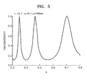
- FIG. 2 is a cross-sectional view of a display apparatus according to exemplary embodiments.
- the display apparatus may include a backlight unit 10 to emit light, a metal thin film 22 and a dielectric multiple thin film 30 which may be disposed on the backlight unit 10.
- the light modulator 20 of FIG. 1 may be disposed on the backlight unit 10 so that the substrate 40 may be oriented above (e.g., upwards) the metal thin film 22. By exposing the substrate 40 upwards, the metal thin film 22 or the dielectric multiple thin film 30 may be protected from external environment.
- the backlight unit 10 may be a direct-light type backlight unit that emits light directly from a lower portion of the light modulator 20, or a lateral-light type backlight unit that emits light from a lateral portion of the light modulator 20 towards the light modulator 20 through a light guide plate (not shown).
- the direct-light type backlight unit and the lateral-light type backlight unit are well known, and thus their details will not be given herein.
- the substrate 40 of the light modulator 20 may be exposed upwards.
- the substrate 40 may be disposed on the backlight unit 10, as illustrated in FIG. 3 .
- a separate protective layer (not shown) may further be provided to protect the dielectric layer 21.
- a display apparatus may include a plurality of pixels with each pixel including a plurality of sub-pixels outputting light beams of different colors.
- each pixel of the display apparatus may include a first sub-pixel outputting a red light beam, a second sub-pixel outputting a green light beam, and a third sub-pixel outputting a blue light beam.
- FIG. 2 and FIG. 3 a single sub-pixel is illustrated.
- the metal thin film 22 and the dielectric multiple thin film 30 may be spaced apart from each other by a predetermined interval.
- Spacers 25 are disposed between the metal thin film 22 and the dielectric multiple thin film 30 to maintain the predetermined interval. Dimensions of the spacers 25 may be determined to increase an area through which light passes as long as the dielectric multiple thin film 30 is supported by the spacers 25, and may be disposed at an edge portion of a sub-pixel.
- the metal thin film 22 may be formed of at least one metal such as, for example, A1, Mo, Cr, Ag, Au, W, Ni, Cu and any combination thereof.
- the dielectric layer 21 may be disposed on a surface of the metal thin film 22, and may be formed of, for example, oxide, nitride or mixtures thereof.
- the dielectric layer 21 may include, for example, a SiO 2 layer.
- the metal thin film 22 may have a thickness of, for example, about 10 to about 20 nm.
- the SiO 2 layer may have a thickness of, for example, about 10 to about 200 nm.
- the dielectric multiple thin film 30 may have a structure in which the first layer 31 having a relatively high refractive index and the second layer 32 having a relatively low refractive index are alternately stacked, as described with reference to FIG. 1 .
- the dielectric multiple thin film 30 may have reflectivity of about 70 to about 80 %, and may have low absorption at a visible light spectral region.
- Each layer of the dielectric multiple thin film 30 may have a thickness of about 10 to about 1000 nm.
- An output color light beam may vary according to a distance 'd' between the dielectric multiple thin film 30 and the metal thin film 22.
- the distance 'd' i.e., height of each of the spacers 25
- the distance 'd' may vary in the range of about 50 to about 1000 nm.
- a red light beam may be output.
- a blue light beam may be output.
- a first thin film M1 and a second thin film M2 are provided, and are spaced apart from each other by an interval 'L'.
- the reflectivity and transmissivity of the first thin film M1 may be r1 and t1, respectively.
- the reflectivity and transmissivity of the second thin film M2 may be r2 and t2, respectively.
- Each of the first thin film M1 and the second thin film M2 may include a multiple thin film.
- the transmissivity of a light beam transmitted through the first thin film M1 and the second thin film M2 may be obtained using Equation 1 below, according to the transmissivity and reflectivity of each thin film, and a phase difference ⁇ due to the interval L.
- t t 1 ⁇ t 2 ⁇ e i ⁇ 1 - r 1 ⁇ r 2 ⁇ e i ⁇ 2 ⁇ ⁇
- the transmissivity when the denominator is minimized, the transmissivity may be maximized.
- the denominator when r1 and r2 are close to 1, and the phase difference ⁇ is integral multiples of 180 degrees, the denominator may be maximized.
- a multiple thin film having excellent reflectivity may be manufactured by using dielectric and metal materials having low absorption at a visible light region, or using a combination of a dielectric multiple thin film in terms of the construction and thickness.
- the light modulator 20 may include the dielectric multiple thin film 30 and a double layer having the metal thin film 22 and the dielectric layer 21.
- the metal thin film 22 may be formed of aluminum (Al) or argon (Ag), and may be formed with a thickness of about 10 to about 20 nm.
- the dielectric layer 21 may be formed of SiO 2 with a thickness of 100 nm.
- An Al metal thin film may have reflectivity of about 80 % and an Ag metal thin film may have reflectivity of about 90 %.
- FIG. 6 is a graph showing the transmissivity T and reflectivity R of a dielectric multiple thin film of a display apparatus with respect to wavelength according to exemplary embodiments. Referring to FIG.
- the dielectric multiple thin film used in FIG. 6 may have a structure in which four layers are formed by alternatively stacking a TiO 2 layer having a thickness 'h1' of 46.3 nm and a refractive index 'n1,' and a SiO 2 layer having a thickness 'h2' of 86.81 nm and a refractive index 'n2.
- Equation I the higher the effective reflectivity of thin films at lower and upper portions of a display apparatus, the higher the optical transmissivity.
- the reflectivity of a dielectric layer and a metal thin film may be about 60 % or more.
- FIG. 8A is a graph showing reflectivity R, transmissivity T, and absorption A with respect to wavelength when a spacer of a display apparatus has a height of 200 nm according to exemplary embodiments.
- the transmissivity of light at a red wavelength band may be relatively high, and the reflectivity of light at the remaining wavelength band (e.g., apart from the wavelengths corresponding to the red band) may be relatively high.
- FIG. 8A is a graph showing reflectivity R, transmissivity T, and absorption A with respect to wavelength when a spacer of a display apparatus has a height of 200 nm according to exemplary embodiments.
- the transmissivity of light at a red wavelength band may be relatively high
- the reflectivity of light at the remaining wavelength band e.g., apart from the wavelengths corresponding to the red band
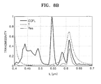
- FIG. 8B is a graph comparing a spectrum of light transmitted through a light modulator of a display apparatus when a spacer has a height of 200 nm with a spectrum of a cold-cathode fluorescent lamp (CCFL), and a 'Res' spectrum corresponding to a result in which the absorption A of FIG. 8A is applied to the transmissivity T of FIG. 8A .
- FIG. 8C shows a color gamut when a spacer of a display apparatus has a height of 200 nm according to exemplary embodiments.
- FIG. 9A is a graph showing reflectivity R, transmissivity T, and absorption A with respect to wavelength when a spacer of a display apparatus has a height of 140 nm according to exemplary embodiments.
- FIG. 9B is a graph providing a comparison of a CCFL spectrum, a transmissivity T spectrum, and a 'Res' spectrum of light transmitted through a light modulator of a display apparatus when a spacer has a height of 140 nm according to exemplary embodiments.
- FIG. 9C shows a color gamut when a spacer of a display apparatus has a height of 140 nm according to exemplary embodiments.
- FIG. 10A is a graph showing reflectivity R, transmissivity T, and absorption A with respect to wavelength when a spacer of a display apparatus has a height of 64 nm according to exemplary embodiments.
- FIG. 10B is a graph providing a comparison of a CCFL spectrum, a transmissivity T spectrum, and a 'Res' spectrum of light transmitted through a light modulator of a display apparatus when a spacer has a height of 64 nm, according to exemplary embodiments.
- FIG. 10C shows a color gamut when a spacer of a display apparatus has a height of 64 nm according to exemplary embodiments.
- the maximum efficiency of transmitted light may be 70% or more, and a transmissive bandwidth may be narrow (e.g., 50 nm or less). Since the transmissive bandwidth is narrow, color properties may be excellent. Since the light modulator 20 uses transparent dielectric thin films except for a metal thin film, optical absorption may generally occur in the metal thin film.
- a backlight unit may use a CCFL light source, and each sub-pixel may emit a corresponding color light beam according to the height of a spacer.
- a dielectric multiple thin film may perform a filtering operation in which only a light beam having a predetermined wavelength may transmit through destructive interference and constructive interference while incident light may be repeatedly reflected and transmitted. Color properties may be adjusted according to the thickness and type of thin film.
- High-purity color may be realized due to a narrow bandwidth.
- the display apparatus does not include any color filter in order to realize colors, manufacturing costs may be reduced, and light use efficiency may be increased, compared to display apparatuses in which a color filter is used.
- FIG. 11 shows color gamut in a display apparatus according to exemplary embodiments.
- the color gamut may be about 66.4 %. Since a liquid crystal or polarization film is not used for FIG. 11 's display apparatus, FIG. 11 's display apparatus may have higher transmissivity than a general liquid crystal display device (LCD).
- LCD liquid crystal display device
- a black mode (off mode) of a display apparatus will now be described.
- the metal thin film 22 may attach to a portion of the dielectric multiple thin film 30 due to an attractive force. Since the metal thin film 22 attaches to the dielectric multiple thin film 30, an interval between the metal thin film 22 and the dielectric multiple thin film 30 may change. Since a transmissive band is shifted to an ultraviolet (UV) region due to the changed interference condition, a beam of visible light may not be transmitted thereby realizing a black color.
- UV ultraviolet
- FIG. 13A is a graph showing transmissivity T, reflectivity R, and absorption A in a black mode of a display apparatus according to exemplary embodiments. Referring to FIG. 13A , the transmissivity may be less than about 0.5 % in the black mode.
- each sub-pixel may include a plurality of cells.
- each sub-pixel may include, for example, about 10 to about 20 cells, and each cell may have horizontal and vertical lengths of about 10 to about 150 ⁇ m.
- Each cell may have materially the same structure as that of a sub-pixel illustrated in FIG. 2 , and may be configured to perform on-off control for each respective cell.
- a gray level may be realized by selectively performing the on-off control on a single sub-pixel in a plurality of cells.
- a display apparatus when light emitted from the backlight unit 10 is incident on the light modulator 20, the scope of the incident angle may not be large. When the scope of the incident light is large, significant color diffusion may occur. According to the exemplary embodiments described herein, significant color diffusion may not occur, since the display apparatus may be controlled so that light emitted from the backlight unit 10 is incident on the light modulator 20 at an angle of about 20 degrees or less.
- An interference light modulator may emit a color light beam without a color filter, and may have higher light use efficiency than that of a liquid crystal optical modulator using a liquid crystal or a polarization film.
- the interference optical modulator may greatly reduce the optical transmissivity in an off mode for realizing a black color, thereby increasing color purity.
- a display apparatus including the interference optical modulator may realize a color image without a color filter, and may be manufactured by low manufacturing costs.
Abstract
Description
- Exemplary embodiments of the present invention relate to an interference light modulator and a display apparatus employing the same.
- Various portable terminals have been developed with advanced communication and display devices. Examples of portable terminals include personal digital assistants (PDAs), portable multimedia players (PMPs), and digital multimedia broadcasting (DMB) devices. Portable terminals have largely used liquid crystal displays (LCDs) as flat display devices thereof. A LCD may include an optical switch by using the birefringence of a liquid crystal, and may realize colors by using a color filter. However, since the LCD uses polarization properties of light, the light use efficiency of the LCD may be low. Further, due to a color filter used in the LCD, the light use efficiency of the LCD may be lower. Since the color filter is expensive, the LCD may also be expensive. Accordingly, there is a demand for a method of creating a color image without a color filter.
- Exemplary embodiments of the present invention relate to an interference optical modulator having excellent light use efficiency.
- Exemplary embodiments of the present invention relate to a display apparatus having excellent light use efficiency and color purity.
- Additional features of the invention will be set forth in the description which follows, and in part will be apparent from the description, or may be learned by practice of the invention.
- Exemplary embodiments of the present invention disclose an interference light modulator comprising a substrate, a dielectric multiple thin film, a metal thin film, and a spacer. The dielectric multiple thin film is disposed on a surface of the substrate. The metal thin film is spaced apart from the dielectric multiple thin film. The spacer supports the dielectric multiple thin film and the metal thin film to maintain an interval between the dielectric multiple thin film and the metal thin film.
- Exemplary embodiments of the present invention disclose a display apparatus comprising a substrate, a dielectric multiple thin film, a metal thin film, a spacer, and a backlight unit. The dielectric multiple thin film is disposed on a surface of the substrate. The metal thin film is spaced apart from the dielectric multiple thin film. The spacer supports the dielectric multiple thin film and the metal thin film to maintain an interval between the dielectric multiple thin film and the metal thin film. The backlight unit emits light towards the substrate or the metal thin film.
- It is to be understood that both the foregoing general description and the following detailed description are exemplary and explanatory and are intended to provide further explanation of the invention as claimed.
- The accompanying drawings, which are included to provide a further understanding of the invention and are incorporated in and constitute a part of this specification, illustrate exemplary embodiments of the invention, and together with the description serve to explain the principles of the invention.
-
FIG. 1 is a cross-sectional view of a light modulator according to exemplary embodiments of the present invention. -
FIG. 2 is a cross-sectional view of a display apparatus according to exemplary embodiments of the present invention. -
FIG. 3 is a cross-sectional view of a light modulator according to exemplary embodiments of the present invention. -
FIG. 4 is a diagram for explaining reflectivity and transmissivity with respect to an interval between two thin films according to exemplary embodiments of the present invention. -
FIG. 5 is a graph showing transmissivity with respect to wavelength when the reflectivity of each thin film ofFIG. 4 is 0.7, and an interval between thin films is 700 nm according to exemplary embodiments of the present invention. -
FIG. 6 is a graph showing transmissivity and reflectivity of a dielectric multiple thin film of a display apparatus with respect to a wavelength according to exemplary embodiments of the present invention. -
FIG. 7 is a graph showing reflectivity, transmissivity, and absorption of a metal thin film of a display apparatus with respect to a wavelength according to exemplary embodiments of the present invention. -
FIG. 8A is a graph showing reflectivity, transmissivity, and absorption with respect to wavelength when a spacer of a display apparatus has a height of 200 nm according to exemplary embodiments of the present invention. -
FIG. 8B is a graph showing a spectrum of light transmitted through a light modulator of a display apparatus when a spacer has a height of 200 nm according to exemplary embodiments of the present invention. -
FIG. 8C shows color gamut when a spacer has a height of 200 nm according to exemplary embodiments of the present invention. -
FIG. 9A is a graph showing reflectivity, transmissivity, and absorption with respect to wavelength when a spacer of a display apparatus has a height of 200 nm according to exemplary embodiments of the present invention. -
FIG. 9B is a graph showing a spectrum of light transmitted through a light modulator of a display apparatus when a spacer has a height of 140 nm according to exemplary embodiments of the present invention. -
FIG. 9C shows color gamut when a spacer of a display apparatus has a height of 140 nm according to exemplary embodiments of the present invention. -
FIG. 10A is a graph showing reflectivity, transmissivity, and absorption with respect to wavelength when a spacer of a display apparatus has a height of 64 nm according to exemplary embodiments of the present invention. -
FIG. 10B is a graph showing a spectrum of light transmitted through a light modulator of a display apparatus when a spacer has a height of 64 nm according to exemplary embodiments of the present invention. -
FIG. 10C shows color gamut when a spacer of a display apparatus has a height of 64 nm according to exemplary embodiments of the present invention. -
FIG. 1 shows color gamut in a display apparatus according to exemplary embodiments of the present invention. -
FIG. 12 is a diagram showing a black mode of a display apparatus according to exemplary embodiments of the present invention. -
FIG. 13A is a graph showing transmissivity, reflectivity, and absorption in a black mode of a display apparatus according to exemplary embodiments of the present invention. -
FIG. 13B is a graph showing a spectrum in a black mode of a display apparatus according to exemplary embodiments of the present invention. - The invention is described more fully hereinafter with reference to the accompanying drawings, in which exemplary embodiments of the invention are shown. This invention may, however, be embodied in many different forms and should not be construed as limited to the exemplary embodiments set forth herein. Rather, these exemplary embodiments are provided so that this disclosure is thorough, and will fully convey the scope of the invention to those skilled in the art. In the drawings, the size and relative sizes of layers and regions may be exaggerated for clarity. Like reference numerals in the drawings denote like elements.
- It will be understood that when an element or layer is referred to as being "on" or "connected to" another element or layer, it can be directly on or directly connected to the other element or layer, or intervening elements or layers may be present. In contrast, when an element is referred to as being "directly on" or "directly connected to" another element or layer, there are no intervening elements or layers present.
- A display apparatus may realize colors by using the interference of light, may embody a switching operation, and may include a micro electronic mechanical system (MEMS) structure. The display apparatus may not include any color filter to realize colors.
-
FIG. 1 is a cross-sectional view of alight modulator 20 according to exemplary embodiments of the present invention. Referring toFIG. 1 , thelight modulator 20 may include asubstrate 40, a dielectric multiplethin film 30 disposed on a surface of thesubstrate 40, and a metalthin film 22 spaced apart from the dielectric multiplethin film 30 by a predetermined interval.Spacers 25 are disposed between the metalthin film 22 and the dielectric multiplethin film 30 to maintain the predetermined interval between the metalthin film 22 and the dielectric multiplethin film 30. - The
substrate 40 may be a glass substrate. The dielectric multiplethin film 30 may have a structure in which a plurality of layers having a large difference between their refractive indexes are alternately stacked. The dielectric multiplethin film 30 may be formed by alternately stacking afirst layer 31 and asecond layer 32 having a large difference between their refractive indexes to constitute a structure having two or more layers. For example, the dielectric multiplethin film 30 may be formed by alternately stacking a TiO2 layer having a high refractive index and a SiO2 layer having a low refractive index to constitute a four-layered structure. The dielectric multiplethin film 30 may function as a high-reflection film with respect to visible light. However, when the metalthin film 22 is spaced apart from the dielectric multiplethin film 30 by a predetermined interval, the dielectric multiplethin film 30 may have high optical transmissivity with respect to a predetermined wavelength. In order to increase the optical transmissivity of the dielectric multiplethin film 30, the dielectric multiplethin film 30 may have a six-layered or eight-layered structure. The metalthin film 22 may be formed of at least one of A1, Mo, Cr, Ag, Au, W, Ni, Cu and alloys thereof. The metalthin film 22 may be formed of a material having low optical absorption. - A
transparent electrode 35, for example, an indium tin oxide (ITO) electrode may be formed between thesubstrate 40 and the dielectric multiplethin film 30, and the metalthin film 22 may function as a counter electrode. Adielectric layer 21 may be further disposed on a surface of the metalthin film 22. Thedielectric layer 21 may be formed of oxide, nitride or mixtures thereof. For example, thedielectric layer 21 may be formed of SiO2. Thedielectric layer 21 may have a thickness of, for example, about 10 to about 200 nm. The thinner thedielectric layer 21, the smaller the optical transmissivity of thedielectric layer 21 in a black mode. Thus, it may be easier to realize a black color. - A method of manufacturing the
light modulator 20 ofFIG. 1 will now be described. Thetransparent electrode 35 may be formed on thesubstrate 40. The dielectric multiplethin film 30 may be formed by alternately stacking, for example, a TiO2 layer and a SiO2 layer to form, in some cases, four layers. It should be understood that any number of suitable alternating layers may be used to form the dielectric multiplethin film 30. Oxide or nitride is patterned to form thespacers 25. In some cases, the oxide may include SiO2. The color of light that may be transmitted through and output from thelight modulator 20 may be adjusted according to the height of each of thespacers 25. After performing the patterning operation, a photoresist may be coated on the dielectric multiplethin film 30 to planarize thespacers 25. The metalthin film 22 may be deposited on thespacers 25 and the photoresist, and thedielectric layer 21 may be deposited on the metalthin film 22. The metalthin film 22 and thedielectric layer 21 may be patterned to form pixels and the photoresist may be removed by etching, for example, wet etching. The thicknesses of thedielectric layer 21 and the metalthin film 22 may be determined according to desired reflective properties, and may be determined to obtain a suitable reflectivity, for example, 80 % or more reflectivity. In addition, the metalthin film 22 may be formed of a metal material having low optical absorption in the visible light spectral region. Thedielectric layer 21 may support the metalthin film 22 while preventing the metalthin film 22 from being damaged. Black color may be realized by adjusting the thickness of thedielectric layer 21 to minimize the amount of transmitted light in a black mode. That is, the optical transmissivity of thedielectric layer 21 may be greatly reduced by reducing the thickness of thedielectric layer 21. -
FIG. 2 is a cross-sectional view of a display apparatus according to exemplary embodiments. Referring toFIG. 2 , the display apparatus may include abacklight unit 10 to emit light, a metalthin film 22 and a dielectric multiplethin film 30 which may be disposed on thebacklight unit 10. InFIG. 2 , thelight modulator 20 ofFIG. 1 may be disposed on thebacklight unit 10 so that thesubstrate 40 may be oriented above (e.g., upwards) the metalthin film 22. By exposing thesubstrate 40 upwards, the metalthin film 22 or the dielectric multiplethin film 30 may be protected from external environment. Thebacklight unit 10 may be a direct-light type backlight unit that emits light directly from a lower portion of thelight modulator 20, or a lateral-light type backlight unit that emits light from a lateral portion of thelight modulator 20 towards thelight modulator 20 through a light guide plate (not shown). The direct-light type backlight unit and the lateral-light type backlight unit are well known, and thus their details will not be given herein. - In
FIG. 2 , thesubstrate 40 of thelight modulator 20 may be exposed upwards. Alternatively, thesubstrate 40 may be disposed on thebacklight unit 10, as illustrated inFIG. 3 . In this case, a separate protective layer (not shown) may further be provided to protect thedielectric layer 21. - A display apparatus may include a plurality of pixels with each pixel including a plurality of sub-pixels outputting light beams of different colors. For example, each pixel of the display apparatus may include a first sub-pixel outputting a red light beam, a second sub-pixel outputting a green light beam, and a third sub-pixel outputting a blue light beam. In
FIG. 2 andFIG. 3 , a single sub-pixel is illustrated. The metalthin film 22 and the dielectric multiplethin film 30 may be spaced apart from each other by a predetermined interval.Spacers 25 are disposed between the metalthin film 22 and the dielectric multiplethin film 30 to maintain the predetermined interval. Dimensions of thespacers 25 may be determined to increase an area through which light passes as long as the dielectric multiplethin film 30 is supported by thespacers 25, and may be disposed at an edge portion of a sub-pixel. - The metal
thin film 22 may be formed of at least one metal such as, for example, A1, Mo, Cr, Ag, Au, W, Ni, Cu and any combination thereof. Thedielectric layer 21 may be disposed on a surface of the metalthin film 22, and may be formed of, for example, oxide, nitride or mixtures thereof. Thedielectric layer 21 may include, for example, a SiO2 layer. The metalthin film 22 may have a thickness of, for example, about 10 to about 20 nm. The SiO2 layer may have a thickness of, for example, about 10 to about 200 nm. - The dielectric multiple
thin film 30 may have a structure in which thefirst layer 31 having a relatively high refractive index and thesecond layer 32 having a relatively low refractive index are alternately stacked, as described with reference toFIG. 1 . For example, the dielectric multiplethin film 30 may have reflectivity of about 70 to about 80 %, and may have low absorption at a visible light spectral region. Each layer of the dielectric multiplethin film 30 may have a thickness of about 10 to about 1000 nm. - An output color light beam may vary according to a distance 'd' between the dielectric multiple
thin film 30 and the metalthin film 22. The distance 'd' (i.e., height of each of the spacers 25) may vary in the range of about 50 to about 1000 nm. For example, when the distance 'd' is 200 nm, a red light beam may be output. In addition, when the distance 'd' is 64 nm, a blue light beam may be output. - Hereinafter, color realization of a display apparatus according to exemplary embodiments will be described.
- Referring to
FIG. 4 , a first thin film M1 and a second thin film M2 are provided, and are spaced apart from each other by an interval 'L'. The reflectivity and transmissivity of the first thin film M1 may be r1 and t1, respectively. The reflectivity and transmissivity of the second thin film M2 may be r2 and t2, respectively. Each of the first thin film M1 and the second thin film M2 may include a multiple thin film. When light proceeds from an external light source towards the second thin film M2 through the first thin film M1, the transmissivity of a light beam transmitted through the first thin film M1 and the second thin film M2 may be obtained usingEquation 1 below, according to the transmissivity and reflectivity of each thin film, and a phase difference ϕ due to the interval L.
- According to
Equation 1, when the denominator is minimized, the transmissivity may be maximized. InEquation 1, when r1 and r2 are close to 1, and the phase difference ϕ is integral multiples of 180 degrees, the denominator may be maximized. For example,FIG. 5 is a graph showing transmissivity with respect to wavelength when r1 = 0.7, r2 = 0.7, and L = 700 nm. Although only two thin films are illustrated inFIG. 4 , a peak position and transmissivity at a predetermined wavelength vary according to the thickness, number, and kind of thin films. In order to obtain high transmissivity at a predetermined wavelength, a multiple thin film having excellent reflectivity may be manufactured by using dielectric and metal materials having low absorption at a visible light region, or using a combination of a dielectric multiple thin film in terms of the construction and thickness. - For example, the
light modulator 20 may include the dielectric multiplethin film 30 and a double layer having the metalthin film 22 and thedielectric layer 21. The metalthin film 22 may be formed of aluminum (Al) or argon (Ag), and may be formed with a thickness of about 10 to about 20 nm. Thedielectric layer 21 may be formed of SiO2 with a thickness of 100 nm. An Al metal thin film may have reflectivity of about 80 % and an Ag metal thin film may have reflectivity of about 90 %.FIG. 6 is a graph showing the transmissivity T and reflectivity R of a dielectric multiple thin film of a display apparatus with respect to wavelength according to exemplary embodiments. Referring toFIG. 6 , the transmissivity T and reflectivity R are shown with respect to light at an incident angle θ of 0 degrees. The dielectric multiple thin film used inFIG. 6 may have a structure in which four layers are formed by alternatively stacking a TiO2 layer having a thickness 'h1' of 46.3 nm and a refractive index 'n1,' and a SiO2 layer having a thickness 'h2' of 86.81 nm and a refractive index 'n2.' 'K' may be the number of stacked layers including a pair of a high-refraction thin film and a low-refraction thin film. In the case of a four-layered structure, K=2.FIG. 7 is a graph showing the reflectivity R, transmissivity T, and absorption A of an Al metal thin film having a thickness 'h1' of 10 nm. According to Equation I, the higher the effective reflectivity of thin films at lower and upper portions of a display apparatus, the higher the optical transmissivity. Referring toFIG. 6 andFIG. 7 , the reflectivity of a dielectric layer and a metal thin film may be about 60 % or more. -
FIG. 8A is a graph showing reflectivity R, transmissivity T, and absorption A with respect to wavelength when a spacer of a display apparatus has a height of 200 nm according to exemplary embodiments. Referring toFIG. 8A , the transmissivity of light at a red wavelength band may be relatively high, and the reflectivity of light at the remaining wavelength band (e.g., apart from the wavelengths corresponding to the red band) may be relatively high.
FIG. 8B is a graph comparing a spectrum of light transmitted through a light modulator of a display apparatus when a spacer has a height of 200 nm with a spectrum of a cold-cathode fluorescent lamp (CCFL), and a 'Res' spectrum corresponding to a result in which the absorption A ofFIG. 8A is applied to the transmissivity T ofFIG. 8A .FIG. 8C shows a color gamut when a spacer of a display apparatus has a height of 200 nm according to exemplary embodiments.
FIG. 9A is a graph showing reflectivity R, transmissivity T, and absorption A with respect to wavelength when a spacer of a display apparatus has a height of 140 nm according to exemplary embodiments.FIG. 9B is a graph providing a comparison of a CCFL spectrum, a transmissivity T spectrum, and a 'Res' spectrum of light transmitted through a light modulator of a display apparatus when a spacer has a height of 140 nm according to exemplary embodiments.FIG. 9C shows a color gamut when a spacer of a display apparatus has a height of 140 nm according to exemplary embodiments.FIG. 10A is a graph showing reflectivity R, transmissivity T, and absorption A with respect to wavelength when a spacer of a display apparatus has a height of 64 nm according to exemplary embodiments.FIG. 10B is a graph providing a comparison of a CCFL spectrum, a transmissivity T spectrum, and a 'Res' spectrum of light transmitted through a light modulator of a display apparatus when a spacer has a height of 64 nm, according to exemplary embodiments.FIG. 10C shows a color gamut when a spacer of a display apparatus has a height of 64 nm according to exemplary embodiments. - Referring to the figures noted above, the maximum efficiency of transmitted light may be 70% or more, and a transmissive bandwidth may be narrow (e.g., 50 nm or less). Since the transmissive bandwidth is narrow, color properties may be excellent. Since the
light modulator 20 uses transparent dielectric thin films except for a metal thin film, optical absorption may generally occur in the metal thin film. A backlight unit may use a CCFL light source, and each sub-pixel may emit a corresponding color light beam according to the height of a spacer. A dielectric multiple thin film may perform a filtering operation in which only a light beam having a predetermined wavelength may transmit through destructive interference and constructive interference while incident light may be repeatedly reflected and transmitted. Color properties may be adjusted according to the thickness and type of thin film. High-purity color may be realized due to a narrow bandwidth. In addition, since the display apparatus does not include any color filter in order to realize colors, manufacturing costs may be reduced, and light use efficiency may be increased, compared to display apparatuses in which a color filter is used. -
FIG. 11 shows color gamut in a display apparatus according to exemplary embodiments. The color gamut may be about 66.4 %. Since a liquid crystal or polarization film is not used forFIG. 11 's display apparatus,FIG. 11 's display apparatus may have higher transmissivity than a general liquid crystal display device (LCD). - A black mode (off mode) of a display apparatus according to exemplary embodiments of the present invention will now be described. Referring to
FIG. 12 , when a voltage is applied between thetransparent electrode 35 and the metalthin film 22, the metalthin film 22 may attach to a portion of the dielectric multiplethin film 30 due to an attractive force. Since the metalthin film 22 attaches to the dielectric multiplethin film 30, an interval between the metalthin film 22 and the dielectric multiplethin film 30 may change. Since a transmissive band is shifted to an ultraviolet (UV) region due to the changed interference condition, a beam of visible light may not be transmitted thereby realizing a black color. When the thickness of a dielectric multiple thin film and the thickness of a dielectric layer are small, the transmissivity of visible light at a black mode decreases. The dielectric multiple thin film and the dielectric layer may be formed with a smaller thickness when they are stacked on a hard substrate such as a glass substrate, compared to a case when the dielectric multiple thin film and the dielectric layer are stacked on a soft substrate.FIG. 13A is a graph showing transmissivity T, reflectivity R, and absorption A in a black mode of a display apparatus according to exemplary embodiments. Referring toFIG. 13A , the transmissivity may be less than about 0.5 % in the black mode.FIG. 13B is a graph showing a spectrum with respect to wavelength in a black mode of a display apparatus according to exemplary embodiments. Since the transmissivity of visible light is very low in the black mode (off mode), and the transmissivity of visible light is very high in an 'on' mode in which colors are realized, a contrast ratio may be very high. On-off switching may be performed by applying or not applying a voltage to each respective pixel. Each sub-pixel may include a plurality of cells. For example, each sub-pixel may include, for example, about 10 to about 20 cells, and each cell may have horizontal and vertical lengths of about 10 to about 150 µm. Each cell may have materially the same structure as that of a sub-pixel illustrated inFIG. 2 , and may be configured to perform on-off control for each respective cell. In addition, a gray level may be realized by selectively performing the on-off control on a single sub-pixel in a plurality of cells. - In a display apparatus, when light emitted from the
backlight unit 10 is incident on thelight modulator 20, the scope of the incident angle may not be large. When the scope of the incident light is large, significant color diffusion may occur. According to the exemplary embodiments described herein, significant color diffusion may not occur, since the display apparatus may be controlled so that light emitted from thebacklight unit 10 is incident on thelight modulator 20 at an angle of about 20 degrees or less. - An interference light modulator may emit a color light beam without a color filter, and may have higher light use efficiency than that of a liquid crystal optical modulator using a liquid crystal or a polarization film. In addition, the interference optical modulator may greatly reduce the optical transmissivity in an off mode for realizing a black color, thereby increasing color purity. A display apparatus including the interference optical modulator may realize a color image without a color filter, and may be manufactured by low manufacturing costs.
- While the inventive concept has been particularly shown and described with reference to exemplary embodiments thereof, it will be apparent to those skilled in the art that various modifications and variations can be made in the present invention without departing from the spirit or scope of the invention. Thus, it is intended that the present invention cover the modifications and variations of this invention provided they come within the scope of the appended claims and their equivalents.
Claims (15)
- An interference light modulator, comprising:a substrate;a dielectric film disposed on a surface of the substrate, the dielectric film comprising at least two layers;;a metal film spaced apart from the dielectric film; anda spacer disposed between the dielectric film and the metal film.
- The interference light modulator of claim 1, wherein the spacer has a height in a range of about 50 nm to about 1000 nm.
- The interference light modulator of claim 1, wherein the metal film comprises at least one metal selected from the group consisting of A1, Mo, Cr, Ag, Au, W, Ni, Cu, and alloys thereof.
- The interference light modulator of claim 1, wherein the dielectric film comprises a first layer and a second layer that are alternately stacked, a refractive index of the first layer differs from a refractive index of the second layer.
- The interference light modulator of claim 1, wherein the substrate comprises a glass substrate.
- The interference light modulator of claim 1, further comprising a dielectric layer disposed on the metal film, the dielectric layer comprising an oxide, a nitride, or a combination of an oxide and a nitride.
- The interference light modulator of claim 6, wherein the dielectric layer comprises a SiO2 layer.
- The interference light modulator of claim 1, wherein each layer of the at least two layers has a thickness in a range of 10 nm to 1000 nm.
- A display apparatus, comprising:a substrate;a dielectric film disposed on a surface of the substrate, the dielectric film comprising at least two layers;a metal film spaced apart from the dielectric film;a spacer disposed between the dielectric film and the metal film; anda backlight unit to emit light towards the substrate or the metal film.
- The display apparatus of claim 9, wherein the spacer has a height in a range of about 50 nm to about 1000 nm.
- The display apparatus of claim 9, wherein the metal film comprises at least one metal selected from the group consisting of Al, Mo, Cr, Ag, Au, W, Ni, Cu and alloys thereof.
- The display apparatus of claim 9, wherein the dielectric film comprises a first layer and a second layer that are alternately stacked, and a refractive index of the first layer differs from a refractive index of the second layer.
- The display apparatus of claim 9, wherein the substrate comprises a glass substrate.
- The display apparatus of claim 9, further comprises a dielectric layer disposed on the metal film, the dielectric layer comprising an oxide, a nitride, or a combination of an oxide and a nitride.
- The display apparatus of claim 14, wherein the dielectric layer comprises a SiO2 layer.
Applications Claiming Priority (1)
| Application Number | Priority Date | Filing Date | Title |
|---|---|---|---|
| KR1020090015869A KR101614903B1 (en) | 2009-02-25 | 2009-02-25 | Interference light modulator and display imploying the same |
Publications (1)
| Publication Number | Publication Date |
|---|---|
| EP2224275A1 true EP2224275A1 (en) | 2010-09-01 |
Family
ID=42145002
Family Applications (1)
| Application Number | Title | Priority Date | Filing Date |
|---|---|---|---|
| EP10001127A Withdrawn EP2224275A1 (en) | 2009-02-25 | 2010-02-04 | Interference light modulator and display apparatus employing the same |
Country Status (5)
| Country | Link |
|---|---|
| US (1) | US8009346B2 (en) |
| EP (1) | EP2224275A1 (en) |
| JP (1) | JP5846719B2 (en) |
| KR (1) | KR101614903B1 (en) |
| CN (1) | CN101813825B (en) |
Cited By (2)
| Publication number | Priority date | Publication date | Assignee | Title |
|---|---|---|---|---|
| WO2013066689A1 (en) * | 2011-11-04 | 2013-05-10 | Qualcomm Mems Technologies, Inc. | Matching layer thin-films for an electromechanical systems reflective display device |
| WO2013165853A1 (en) * | 2012-05-03 | 2013-11-07 | Qualcomm Mems Technologies, Inc. | Grey scale electromechanical systems display device |
Families Citing this family (9)
| Publication number | Priority date | Publication date | Assignee | Title |
|---|---|---|---|---|
| JP5625614B2 (en) | 2010-08-20 | 2014-11-19 | セイコーエプソン株式会社 | Optical filter, optical filter module, spectrophotometer and optical instrument |
| US20120056890A1 (en) * | 2010-09-02 | 2012-03-08 | Qualcomm Mems Technologies, Inc. | Flexible film interferometric modulator devices and methods of forming the same |
| TWI457615B (en) * | 2011-04-25 | 2014-10-21 | E Ink Holdings Inc | Color filter, optical grating structure and display module |
| JP5910099B2 (en) | 2012-01-18 | 2016-04-27 | セイコーエプソン株式会社 | Interference filters, optical modules and electronics |
| US8605351B1 (en) | 2012-06-27 | 2013-12-10 | The United States Of America As Represented By The Secretary Of The Navy | Transparent interferometric visible spectrum modulator |
| CN102749667B (en) * | 2012-07-28 | 2014-09-17 | 杭州科汀光学技术有限公司 | Optical filter for image chip |
| JP5999159B2 (en) * | 2014-10-01 | 2016-09-28 | セイコーエプソン株式会社 | Optical filter, optical filter module, spectrophotometer and optical instrument |
| US10884314B2 (en) * | 2015-02-05 | 2021-01-05 | Sharp Kabushiki Kaisha | Solid state reflective display |
| KR102374120B1 (en) * | 2015-09-23 | 2022-03-14 | 삼성전자주식회사 | Mirror display and method of manufacturing the same |
Citations (1)
| Publication number | Priority date | Publication date | Assignee | Title |
|---|---|---|---|---|
| US20040125281A1 (en) * | 2002-12-25 | 2004-07-01 | Wen-Jian Lin | Optical interference type of color display |
Family Cites Families (26)
| Publication number | Priority date | Publication date | Assignee | Title |
|---|---|---|---|---|
| TW357271B (en) * | 1996-02-26 | 1999-05-01 | Seiko Epson Corp | Light regulator, display and the electronic machine |
| KR20020010322A (en) | 2000-07-29 | 2002-02-04 | 구본준, 론 위라하디락사 | Display device using micro electro-mechanical system |
| JP2002062505A (en) * | 2000-08-14 | 2002-02-28 | Canon Inc | Projection type display deice and interference modulation element used therefor |
| JP2002174780A (en) * | 2000-12-08 | 2002-06-21 | Stanley Electric Co Ltd | Reflection type color display device |
| JP2003057567A (en) | 2001-08-16 | 2003-02-26 | Sony Corp | Optical multi-layered structure, optical switching element and its manufacturing method, and image display device |
| JP3893421B2 (en) | 2001-12-27 | 2007-03-14 | 富士フイルム株式会社 | Light modulation element, light modulation element array, and exposure apparatus using the same |
| JP4470903B2 (en) * | 2002-03-22 | 2010-06-02 | セイコーエプソン株式会社 | projector |
| TW594155B (en) * | 2002-12-27 | 2004-06-21 | Prime View Int Corp Ltd | Optical interference type color display and optical interference modulator |
| JP2004212674A (en) | 2002-12-27 | 2004-07-29 | Fuji Photo Film Co Ltd | Two-dimensional matrix flat display element and its driving method |
| JP4243201B2 (en) | 2003-01-17 | 2009-03-25 | 富士フイルム株式会社 | Light modulation element, light modulation element array, image forming apparatus and flat display apparatus |
| US7233029B2 (en) | 2003-01-17 | 2007-06-19 | Fujifilm Corporation | Optical functional film, method of forming the same, and spatial light modulator, spatial light modulator array, image forming device and flat panel display using the same |
| TW594360B (en) | 2003-04-21 | 2004-06-21 | Prime View Int Corp Ltd | A method for fabricating an interference display cell |
| TWI226504B (en) * | 2003-04-21 | 2005-01-11 | Prime View Int Co Ltd | A structure of an interference display cell |
| TWI230801B (en) | 2003-08-29 | 2005-04-11 | Prime View Int Co Ltd | Reflective display unit using interferometric modulation and manufacturing method thereof |
| JP2005157133A (en) * | 2003-11-27 | 2005-06-16 | Okayama Prefecture | Optical switching element and image display apparatus using optical switching element |
| JP4452560B2 (en) | 2004-06-07 | 2010-04-21 | 富士フイルム株式会社 | Transmission type light modulation element and transmission type light modulation array element |
| CN101006490A (en) * | 2004-08-27 | 2007-07-25 | Idc公司 | Current mode display driver circuit realization feature |
| US20060066932A1 (en) * | 2004-09-27 | 2006-03-30 | Clarence Chui | Method of selective etching using etch stop layer |
| US7710632B2 (en) * | 2004-09-27 | 2010-05-04 | Qualcomm Mems Technologies, Inc. | Display device having an array of spatial light modulators with integrated color filters |
| US7355780B2 (en) * | 2004-09-27 | 2008-04-08 | Idc, Llc | System and method of illuminating interferometric modulators using backlighting |
| JP4414855B2 (en) | 2004-09-30 | 2010-02-10 | 富士フイルム株式会社 | Manufacturing method of transmissive light modulation element |
| JP4862460B2 (en) * | 2006-04-04 | 2012-01-25 | ソニー株式会社 | Reflective liquid crystal display element, manufacturing method thereof, and liquid crystal display device |
| JP2008145506A (en) * | 2006-12-06 | 2008-06-26 | Institute Of National Colleges Of Technology Japan | Optical element using piezoelectric element, and method of forming the same |
| KR101269250B1 (en) | 2007-04-09 | 2013-05-29 | 한양대학교 산학협력단 | The light modulator for flat panel display |
| JP4633088B2 (en) | 2007-06-04 | 2011-02-16 | シャープ株式会社 | Interferometric modulator and display device |
| JP5082648B2 (en) * | 2007-07-24 | 2012-11-28 | カシオ計算機株式会社 | IMAGING DEVICE, IMAGING DEVICE CONTROL PROGRAM, AND IMAGING DEVICE CONTROL METHOD |
-
2009
- 2009-02-25 KR KR1020090015869A patent/KR101614903B1/en active IP Right Grant
-
2010
- 2010-01-25 US US12/693,064 patent/US8009346B2/en not_active Expired - Fee Related
- 2010-02-04 EP EP10001127A patent/EP2224275A1/en not_active Withdrawn
- 2010-02-23 JP JP2010037375A patent/JP5846719B2/en not_active Expired - Fee Related
- 2010-02-25 CN CN201010126163.6A patent/CN101813825B/en not_active Expired - Fee Related
Patent Citations (1)
| Publication number | Priority date | Publication date | Assignee | Title |
|---|---|---|---|---|
| US20040125281A1 (en) * | 2002-12-25 | 2004-07-01 | Wen-Jian Lin | Optical interference type of color display |
Non-Patent Citations (1)
| Title |
|---|
| ANONYMOUS: "Dielectric mirror", WIKIPEDIA, THE FREE ENCYCLOPEDIA, 14 February 2009 (2009-02-14), XP055214237, Retrieved from the Internet <URL:https://en.wikipedia.org/w/index.php?title=Dielectric_mirror&oldid=270631605> [retrieved on 20150917] * |
Cited By (4)
| Publication number | Priority date | Publication date | Assignee | Title |
|---|---|---|---|---|
| WO2013066689A1 (en) * | 2011-11-04 | 2013-05-10 | Qualcomm Mems Technologies, Inc. | Matching layer thin-films for an electromechanical systems reflective display device |
| US8736939B2 (en) | 2011-11-04 | 2014-05-27 | Qualcomm Mems Technologies, Inc. | Matching layer thin-films for an electromechanical systems reflective display device |
| US9081188B2 (en) | 2011-11-04 | 2015-07-14 | Qualcomm Mems Technologies, Inc. | Matching layer thin-films for an electromechanical systems reflective display device |
| WO2013165853A1 (en) * | 2012-05-03 | 2013-11-07 | Qualcomm Mems Technologies, Inc. | Grey scale electromechanical systems display device |
Also Published As
| Publication number | Publication date |
|---|---|
| KR20100096809A (en) | 2010-09-02 |
| US20100214644A1 (en) | 2010-08-26 |
| JP2010198018A (en) | 2010-09-09 |
| CN101813825B (en) | 2014-02-12 |
| KR101614903B1 (en) | 2016-04-25 |
| US8009346B2 (en) | 2011-08-30 |
| JP5846719B2 (en) | 2016-01-20 |
| CN101813825A (en) | 2010-08-25 |
Similar Documents
| Publication | Publication Date | Title |
|---|---|---|
| US8009346B2 (en) | Interference light modulator and display apparatus employing the same | |
| JP4778873B2 (en) | Liquid crystal display | |
| JP3979982B2 (en) | Interferometric modulator and display device | |
| JP3201990B2 (en) | Reflective liquid crystal cell without flicker | |
| JP2005308871A (en) | Interference color filter | |
| JP2005173037A (en) | Liquid crystal display device and its manufacturing method | |
| JP5692909B2 (en) | Reflective color filter and display device including the same | |
| WO2015039557A1 (en) | Reflective optical filter, manufacturing method therefor and display device using same | |
| US20240012247A1 (en) | Wide Angle Waveguide Display | |
| US20130033678A1 (en) | Optical element, light source device, and projection display device | |
| US20230266512A1 (en) | Nanoparticle-Based Holographic Photopolymer Materials and Related Applications | |
| CN109143659B (en) | Reflection type color display based on spiral photonic crystal and manufacturing method thereof | |
| US10761362B2 (en) | Display panel and display device | |
| CN111796452A (en) | Liquid crystal display panel | |
| CN110646980B (en) | Liquid crystal display | |
| JP4633088B2 (en) | Interferometric modulator and display device | |
| CN110264881B (en) | Display device and manufacturing method | |
| KR20100040650A (en) | Photonic crystal type optical filter, reflective type color filter, transflective type color filter and display device using the same | |
| US6317179B1 (en) | Reflection type display and coloring method thereof | |
| JP3941322B2 (en) | Electrode substrate for reflective liquid crystal display device and reflective liquid crystal display device using the same | |
| CN113391485A (en) | Array substrate, manufacturing method and display panel | |
| JP2003149632A (en) | Liquid crystal display device and color filter therefor | |
| JP2010039038A (en) | Display device | |
| JP2009092972A (en) | Display device | |
| JP2013164429A (en) | Color filter and reflection type display device including the same |
Legal Events
| Date | Code | Title | Description |
|---|---|---|---|
| PUAI | Public reference made under article 153(3) epc to a published international application that has entered the european phase |
Free format text: ORIGINAL CODE: 0009012 |
|
| AK | Designated contracting states |
Kind code of ref document: A1 Designated state(s): AT BE BG CH CY CZ DE DK EE ES FI FR GB GR HR HU IE IS IT LI LT LU LV MC MK MT NL NO PL PT RO SE SI SK SM TR |
|
| AX | Request for extension of the european patent |
Extension state: AL BA RS |
|
| 17P | Request for examination filed |
Effective date: 20110225 |
|
| RAP1 | Party data changed (applicant data changed or rights of an application transferred) |
Owner name: SAMSUNG ELECTRONICS CO., LTD. |
|
| RAP1 | Party data changed (applicant data changed or rights of an application transferred) |
Owner name: SAMSUNG DISPLAY CO., LTD. |
|
| RAP1 | Party data changed (applicant data changed or rights of an application transferred) |
Owner name: SAMSUNG DISPLAY CO., LTD. |
|
| 17Q | First examination report despatched |
Effective date: 20150925 |
|
| GRAP | Despatch of communication of intention to grant a patent |
Free format text: ORIGINAL CODE: EPIDOSNIGR1 |
|
| INTG | Intention to grant announced |
Effective date: 20170704 |
|
| RIN1 | Information on inventor provided before grant (corrected) |
Inventor name: PRUDNIKOV, OLEG Inventor name: CHEONG, BYOUNG-HO |
|
| STAA | Information on the status of an ep patent application or granted ep patent |
Free format text: STATUS: THE APPLICATION IS DEEMED TO BE WITHDRAWN |
|
| 18D | Application deemed to be withdrawn |
Effective date: 20171115 |