EP2176407B1 - Method of patterning a substrate - Google Patents
Method of patterning a substrate Download PDFInfo
- Publication number
- EP2176407B1 EP2176407B1 EP08771860.7A EP08771860A EP2176407B1 EP 2176407 B1 EP2176407 B1 EP 2176407B1 EP 08771860 A EP08771860 A EP 08771860A EP 2176407 B1 EP2176407 B1 EP 2176407B1
- Authority
- EP
- European Patent Office
- Prior art keywords
- layer
- thermal transfer
- transfer layer
- receptor
- donor
- Prior art date
- Legal status (The legal status is an assumption and is not a legal conclusion. Google has not performed a legal analysis and makes no representation as to the accuracy of the status listed.)
- Active
Links
- 238000000034 method Methods 0.000 title claims description 73
- 239000000758 substrate Substances 0.000 title claims description 61
- 238000000059 patterning Methods 0.000 title description 14
- 239000010410 layer Substances 0.000 claims description 344
- 238000012546 transfer Methods 0.000 claims description 210
- 239000000463 material Substances 0.000 claims description 129
- 230000003197 catalytic effect Effects 0.000 claims description 51
- 239000007769 metal material Substances 0.000 claims description 51
- 239000011229 interlayer Substances 0.000 claims description 44
- 239000012018 catalyst precursor Substances 0.000 claims description 43
- 239000011230 binding agent Substances 0.000 claims description 26
- 238000006243 chemical reaction Methods 0.000 claims description 23
- 238000000151 deposition Methods 0.000 claims description 23
- 238000004132 cross linking Methods 0.000 claims description 3
- 229910052751 metal Inorganic materials 0.000 description 59
- 239000002184 metal Substances 0.000 description 59
- KDLHZDBZIXYQEI-UHFFFAOYSA-N Palladium Chemical compound [Pd] KDLHZDBZIXYQEI-UHFFFAOYSA-N 0.000 description 35
- 238000000576 coating method Methods 0.000 description 34
- 229920000642 polymer Polymers 0.000 description 34
- 239000011248 coating agent Substances 0.000 description 29
- 239000000243 solution Substances 0.000 description 29
- 230000005855 radiation Effects 0.000 description 24
- 239000002904 solvent Substances 0.000 description 21
- 239000010408 film Substances 0.000 description 20
- 238000003384 imaging method Methods 0.000 description 19
- 230000008021 deposition Effects 0.000 description 18
- 239000006100 radiation absorber Substances 0.000 description 18
- 239000003054 catalyst Substances 0.000 description 17
- -1 for example Polymers 0.000 description 15
- 150000002739 metals Chemical class 0.000 description 15
- IJGRMHOSHXDMSA-UHFFFAOYSA-N Atomic nitrogen Chemical compound N#N IJGRMHOSHXDMSA-UHFFFAOYSA-N 0.000 description 14
- 238000007772 electroless plating Methods 0.000 description 14
- 238000007747 plating Methods 0.000 description 14
- 230000008569 process Effects 0.000 description 14
- BQCADISMDOOEFD-UHFFFAOYSA-N Silver Chemical compound [Ag] BQCADISMDOOEFD-UHFFFAOYSA-N 0.000 description 13
- XKRFYHLGVUSROY-UHFFFAOYSA-N argon Substances [Ar] XKRFYHLGVUSROY-UHFFFAOYSA-N 0.000 description 13
- 239000003638 chemical reducing agent Substances 0.000 description 13
- 229910052763 palladium Inorganic materials 0.000 description 13
- 239000000126 substance Substances 0.000 description 13
- 238000010276 construction Methods 0.000 description 12
- 238000010438 heat treatment Methods 0.000 description 12
- 239000000975 dye Substances 0.000 description 11
- ZWEHNKRNPOVVGH-UHFFFAOYSA-N 2-Butanone Chemical compound CCC(C)=O ZWEHNKRNPOVVGH-UHFFFAOYSA-N 0.000 description 10
- RYGMFSIKBFXOCR-UHFFFAOYSA-N Copper Chemical compound [Cu] RYGMFSIKBFXOCR-UHFFFAOYSA-N 0.000 description 10
- 229910052802 copper Inorganic materials 0.000 description 10
- 239000010949 copper Substances 0.000 description 10
- BASFCYQUMIYNBI-UHFFFAOYSA-N platinum Chemical compound [Pt] BASFCYQUMIYNBI-UHFFFAOYSA-N 0.000 description 10
- 238000006722 reduction reaction Methods 0.000 description 10
- PXHVJJICTQNCMI-UHFFFAOYSA-N Nickel Chemical compound [Ni] PXHVJJICTQNCMI-UHFFFAOYSA-N 0.000 description 9
- 239000011521 glass Substances 0.000 description 9
- 229920005992 thermoplastic resin Polymers 0.000 description 8
- 230000003213 activating effect Effects 0.000 description 7
- 239000012790 adhesive layer Substances 0.000 description 7
- 229910052786 argon Inorganic materials 0.000 description 7
- 229910052757 nitrogen Inorganic materials 0.000 description 7
- 230000009467 reduction Effects 0.000 description 7
- 150000003839 salts Chemical class 0.000 description 7
- 229920005479 Lucite® Polymers 0.000 description 6
- HEMHJVSKTPXQMS-UHFFFAOYSA-M Sodium hydroxide Chemical compound [OH-].[Na+] HEMHJVSKTPXQMS-UHFFFAOYSA-M 0.000 description 6
- ATJFFYVFTNAWJD-UHFFFAOYSA-N Tin Chemical compound [Sn] ATJFFYVFTNAWJD-UHFFFAOYSA-N 0.000 description 6
- 230000008901 benefit Effects 0.000 description 6
- 239000006229 carbon black Substances 0.000 description 6
- 239000002105 nanoparticle Substances 0.000 description 6
- 230000003287 optical effect Effects 0.000 description 6
- 239000000049 pigment Substances 0.000 description 6
- 229920002037 poly(vinyl butyral) polymer Polymers 0.000 description 6
- 239000004926 polymethyl methacrylate Substances 0.000 description 6
- 239000011347 resin Substances 0.000 description 6
- 229910052709 silver Inorganic materials 0.000 description 6
- 239000004332 silver Substances 0.000 description 6
- 229910052718 tin Inorganic materials 0.000 description 6
- UHFFVFAKEGKNAQ-UHFFFAOYSA-N 2-benzyl-2-(dimethylamino)-1-(4-morpholin-4-ylphenyl)butan-1-one Chemical compound C=1C=C(N2CCOCC2)C=CC=1C(=O)C(CC)(N(C)C)CC1=CC=CC=C1 UHFFVFAKEGKNAQ-UHFFFAOYSA-N 0.000 description 5
- OKTJSMMVPCPJKN-UHFFFAOYSA-N Carbon Chemical compound [C] OKTJSMMVPCPJKN-UHFFFAOYSA-N 0.000 description 5
- 229910052782 aluminium Inorganic materials 0.000 description 5
- XAGFODPZIPBFFR-UHFFFAOYSA-N aluminium Chemical compound [Al] XAGFODPZIPBFFR-UHFFFAOYSA-N 0.000 description 5
- PCHJSUWPFVWCPO-UHFFFAOYSA-N gold Chemical compound [Au] PCHJSUWPFVWCPO-UHFFFAOYSA-N 0.000 description 5
- 229910052737 gold Inorganic materials 0.000 description 5
- 239000010931 gold Substances 0.000 description 5
- 239000000203 mixture Substances 0.000 description 5
- 229910052759 nickel Inorganic materials 0.000 description 5
- 239000011368 organic material Substances 0.000 description 5
- YJVFFLUZDVXJQI-UHFFFAOYSA-L palladium(ii) acetate Chemical compound [Pd+2].CC([O-])=O.CC([O-])=O YJVFFLUZDVXJQI-UHFFFAOYSA-L 0.000 description 5
- 229910052697 platinum Inorganic materials 0.000 description 5
- 229920000058 polyacrylate Polymers 0.000 description 5
- 229920000139 polyethylene terephthalate Polymers 0.000 description 5
- 239000005020 polyethylene terephthalate Substances 0.000 description 5
- 229920006254 polymer film Polymers 0.000 description 5
- 239000002243 precursor Substances 0.000 description 5
- 229920005989 resin Polymers 0.000 description 5
- 239000010409 thin film Substances 0.000 description 5
- OAKJQQAXSVQMHS-UHFFFAOYSA-N Hydrazine Chemical compound NN OAKJQQAXSVQMHS-UHFFFAOYSA-N 0.000 description 4
- XEEYBQQBJWHFJM-UHFFFAOYSA-N Iron Chemical compound [Fe] XEEYBQQBJWHFJM-UHFFFAOYSA-N 0.000 description 4
- HCHKCACWOHOZIP-UHFFFAOYSA-N Zinc Chemical compound [Zn] HCHKCACWOHOZIP-UHFFFAOYSA-N 0.000 description 4
- 230000006378 damage Effects 0.000 description 4
- 239000006185 dispersion Substances 0.000 description 4
- 238000005530 etching Methods 0.000 description 4
- 230000006870 function Effects 0.000 description 4
- 229910052738 indium Inorganic materials 0.000 description 4
- APFVFJFRJDLVQX-UHFFFAOYSA-N indium atom Chemical compound [In] APFVFJFRJDLVQX-UHFFFAOYSA-N 0.000 description 4
- 229910044991 metal oxide Inorganic materials 0.000 description 4
- 150000004706 metal oxides Chemical class 0.000 description 4
- 230000005012 migration Effects 0.000 description 4
- 238000013508 migration Methods 0.000 description 4
- 229910000510 noble metal Inorganic materials 0.000 description 4
- 229920000767 polyaniline Polymers 0.000 description 4
- 238000012545 processing Methods 0.000 description 4
- 230000002829 reductive effect Effects 0.000 description 4
- 239000007787 solid Substances 0.000 description 4
- 239000004094 surface-active agent Substances 0.000 description 4
- 229920001169 thermoplastic Polymers 0.000 description 4
- XLYOFNOQVPJJNP-UHFFFAOYSA-N water Substances O XLYOFNOQVPJJNP-UHFFFAOYSA-N 0.000 description 4
- 229910052725 zinc Inorganic materials 0.000 description 4
- 239000011701 zinc Substances 0.000 description 4
- WSFSSNUMVMOOMR-UHFFFAOYSA-N Formaldehyde Chemical compound O=C WSFSSNUMVMOOMR-UHFFFAOYSA-N 0.000 description 3
- KJTLSVCANCCWHF-UHFFFAOYSA-N Ruthenium Chemical compound [Ru] KJTLSVCANCCWHF-UHFFFAOYSA-N 0.000 description 3
- YXFVVABEGXRONW-UHFFFAOYSA-N Toluene Chemical compound CC1=CC=CC=C1 YXFVVABEGXRONW-UHFFFAOYSA-N 0.000 description 3
- 238000003848 UV Light-Curing Methods 0.000 description 3
- 239000006096 absorbing agent Substances 0.000 description 3
- 239000011358 absorbing material Substances 0.000 description 3
- 239000000654 additive Substances 0.000 description 3
- 229910017052 cobalt Inorganic materials 0.000 description 3
- 239000010941 cobalt Substances 0.000 description 3
- GUTLYIVDDKVIGB-UHFFFAOYSA-N cobalt atom Chemical compound [Co] GUTLYIVDDKVIGB-UHFFFAOYSA-N 0.000 description 3
- 150000001875 compounds Chemical class 0.000 description 3
- 238000010168 coupling process Methods 0.000 description 3
- 238000005859 coupling reaction Methods 0.000 description 3
- 239000002270 dispersing agent Substances 0.000 description 3
- 238000004090 dissolution Methods 0.000 description 3
- 230000000694 effects Effects 0.000 description 3
- 238000005516 engineering process Methods 0.000 description 3
- 230000004927 fusion Effects 0.000 description 3
- 239000010439 graphite Substances 0.000 description 3
- 229910002804 graphite Inorganic materials 0.000 description 3
- 239000000976 ink Substances 0.000 description 3
- 229910052741 iridium Inorganic materials 0.000 description 3
- GKOZUEZYRPOHIO-UHFFFAOYSA-N iridium atom Chemical compound [Ir] GKOZUEZYRPOHIO-UHFFFAOYSA-N 0.000 description 3
- 238000004519 manufacturing process Methods 0.000 description 3
- 150000002736 metal compounds Chemical class 0.000 description 3
- WSFSSNUMVMOOMR-NJFSPNSNSA-N methanone Chemical compound O=[14CH2] WSFSSNUMVMOOMR-NJFSPNSNSA-N 0.000 description 3
- 238000001000 micrograph Methods 0.000 description 3
- 239000000178 monomer Substances 0.000 description 3
- 239000002245 particle Substances 0.000 description 3
- 229920001197 polyacetylene Polymers 0.000 description 3
- 229910052703 rhodium Inorganic materials 0.000 description 3
- 239000010948 rhodium Substances 0.000 description 3
- MHOVAHRLVXNVSD-UHFFFAOYSA-N rhodium atom Chemical compound [Rh] MHOVAHRLVXNVSD-UHFFFAOYSA-N 0.000 description 3
- 229910052707 ruthenium Inorganic materials 0.000 description 3
- 241000894007 species Species 0.000 description 3
- 229920001909 styrene-acrylic polymer Polymers 0.000 description 3
- 238000002207 thermal evaporation Methods 0.000 description 3
- 239000012815 thermoplastic material Substances 0.000 description 3
- 229920001187 thermosetting polymer Polymers 0.000 description 3
- 238000011282 treatment Methods 0.000 description 3
- 125000005259 triarylamine group Chemical group 0.000 description 3
- 238000009281 ultraviolet germicidal irradiation Methods 0.000 description 3
- QNODIIQQMGDSEF-UHFFFAOYSA-N (1-hydroxycyclohexyl)-phenylmethanone Chemical compound C=1C=CC=CC=1C(=O)C1(O)CCCCC1 QNODIIQQMGDSEF-UHFFFAOYSA-N 0.000 description 2
- ARXJGSRGQADJSQ-UHFFFAOYSA-N 1-methoxypropan-2-ol Chemical compound COCC(C)O ARXJGSRGQADJSQ-UHFFFAOYSA-N 0.000 description 2
- 229920002799 BoPET Polymers 0.000 description 2
- ZOXJGFHDIHLPTG-UHFFFAOYSA-N Boron Chemical compound [B] ZOXJGFHDIHLPTG-UHFFFAOYSA-N 0.000 description 2
- VYZAMTAEIAYCRO-UHFFFAOYSA-N Chromium Chemical compound [Cr] VYZAMTAEIAYCRO-UHFFFAOYSA-N 0.000 description 2
- 239000004593 Epoxy Substances 0.000 description 2
- WOBHKFSMXKNTIM-UHFFFAOYSA-N Hydroxyethyl methacrylate Chemical compound CC(=C)C(=O)OCCO WOBHKFSMXKNTIM-UHFFFAOYSA-N 0.000 description 2
- 229920005731 JONCRYL® 67 Polymers 0.000 description 2
- ZOKXTWBITQBERF-UHFFFAOYSA-N Molybdenum Chemical compound [Mo] ZOKXTWBITQBERF-UHFFFAOYSA-N 0.000 description 2
- 229920001609 Poly(3,4-ethylenedioxythiophene) Polymers 0.000 description 2
- 239000004642 Polyimide Substances 0.000 description 2
- 239000004793 Polystyrene Substances 0.000 description 2
- BLRPTPMANUNPDV-UHFFFAOYSA-N Silane Chemical compound [SiH4] BLRPTPMANUNPDV-UHFFFAOYSA-N 0.000 description 2
- VYPSYNLAJGMNEJ-UHFFFAOYSA-N Silicium dioxide Chemical compound O=[Si]=O VYPSYNLAJGMNEJ-UHFFFAOYSA-N 0.000 description 2
- GWEVSGVZZGPLCZ-UHFFFAOYSA-N Titan oxide Chemical compound O=[Ti]=O GWEVSGVZZGPLCZ-UHFFFAOYSA-N 0.000 description 2
- RTAQQCXQSZGOHL-UHFFFAOYSA-N Titanium Chemical compound [Ti] RTAQQCXQSZGOHL-UHFFFAOYSA-N 0.000 description 2
- QCWXUUIWCKQGHC-UHFFFAOYSA-N Zirconium Chemical compound [Zr] QCWXUUIWCKQGHC-UHFFFAOYSA-N 0.000 description 2
- 239000002253 acid Substances 0.000 description 2
- NIXOWILDQLNWCW-UHFFFAOYSA-N acrylic acid group Chemical group C(C=C)(=O)O NIXOWILDQLNWCW-UHFFFAOYSA-N 0.000 description 2
- 238000003491 array Methods 0.000 description 2
- 230000004888 barrier function Effects 0.000 description 2
- 230000015572 biosynthetic process Effects 0.000 description 2
- 229910052797 bismuth Inorganic materials 0.000 description 2
- JCXGWMGPZLAOME-UHFFFAOYSA-N bismuth atom Chemical compound [Bi] JCXGWMGPZLAOME-UHFFFAOYSA-N 0.000 description 2
- 229910052796 boron Inorganic materials 0.000 description 2
- 229910052804 chromium Inorganic materials 0.000 description 2
- 239000011651 chromium Substances 0.000 description 2
- 238000001246 colloidal dispersion Methods 0.000 description 2
- 229920001940 conductive polymer Polymers 0.000 description 2
- 150000004696 coordination complex Chemical class 0.000 description 2
- 238000001723 curing Methods 0.000 description 2
- 238000005137 deposition process Methods 0.000 description 2
- 150000008049 diazo compounds Chemical class 0.000 description 2
- 238000006073 displacement reaction Methods 0.000 description 2
- 238000009472 formulation Methods 0.000 description 2
- RBTKNAXYKSUFRK-UHFFFAOYSA-N heliogen blue Chemical compound [Cu].[N-]1C2=C(C=CC=C3)C3=C1N=C([N-]1)C3=CC=CC=C3C1=NC([N-]1)=C(C=CC=C3)C3=C1N=C([N-]1)C3=CC=CC=C3C1=N2 RBTKNAXYKSUFRK-UHFFFAOYSA-N 0.000 description 2
- BHEPBYXIRTUNPN-UHFFFAOYSA-N hydridophosphorus(.) (triplet) Chemical compound [PH] BHEPBYXIRTUNPN-UHFFFAOYSA-N 0.000 description 2
- AMGQUBHHOARCQH-UHFFFAOYSA-N indium;oxotin Chemical compound [In].[Sn]=O AMGQUBHHOARCQH-UHFFFAOYSA-N 0.000 description 2
- 229910052742 iron Inorganic materials 0.000 description 2
- 239000003446 ligand Substances 0.000 description 2
- 230000000670 limiting effect Effects 0.000 description 2
- 230000007246 mechanism Effects 0.000 description 2
- 239000002082 metal nanoparticle Substances 0.000 description 2
- 229910052976 metal sulfide Inorganic materials 0.000 description 2
- 229910052750 molybdenum Inorganic materials 0.000 description 2
- 239000011733 molybdenum Substances 0.000 description 2
- 229920003986 novolac Polymers 0.000 description 2
- 229910052762 osmium Inorganic materials 0.000 description 2
- SYQBFIAQOQZEGI-UHFFFAOYSA-N osmium atom Chemical compound [Os] SYQBFIAQOQZEGI-UHFFFAOYSA-N 0.000 description 2
- 230000001590 oxidative effect Effects 0.000 description 2
- 230000036961 partial effect Effects 0.000 description 2
- 238000009832 plasma treatment Methods 0.000 description 2
- 229920000728 polyester Polymers 0.000 description 2
- 229920006267 polyester film Polymers 0.000 description 2
- 239000011112 polyethylene naphthalate Substances 0.000 description 2
- 229920001721 polyimide Polymers 0.000 description 2
- 229920005596 polymer binder Polymers 0.000 description 2
- 239000002491 polymer binding agent Substances 0.000 description 2
- 229920000193 polymethacrylate Polymers 0.000 description 2
- 229920002223 polystyrene Polymers 0.000 description 2
- 229920000123 polythiophene Polymers 0.000 description 2
- 229920002635 polyurethane Polymers 0.000 description 2
- 239000004814 polyurethane Substances 0.000 description 2
- HXHCOXPZCUFAJI-UHFFFAOYSA-N prop-2-enoic acid;styrene Chemical compound OC(=O)C=C.C=CC1=CC=CC=C1 HXHCOXPZCUFAJI-UHFFFAOYSA-N 0.000 description 2
- 229910052702 rhenium Inorganic materials 0.000 description 2
- WUAPFZMCVAUBPE-UHFFFAOYSA-N rhenium atom Chemical compound [Re] WUAPFZMCVAUBPE-UHFFFAOYSA-N 0.000 description 2
- 238000007650 screen-printing Methods 0.000 description 2
- 229910000077 silane Inorganic materials 0.000 description 2
- 239000002356 single layer Substances 0.000 description 2
- 238000001228 spectrum Methods 0.000 description 2
- 238000004544 sputter deposition Methods 0.000 description 2
- SKRWFPLZQAAQSU-UHFFFAOYSA-N stibanylidynetin;hydrate Chemical compound O.[Sn].[Sb] SKRWFPLZQAAQSU-UHFFFAOYSA-N 0.000 description 2
- 150000003440 styrenes Chemical class 0.000 description 2
- 229910052714 tellurium Inorganic materials 0.000 description 2
- PORWMNRCUJJQNO-UHFFFAOYSA-N tellurium atom Chemical compound [Te] PORWMNRCUJJQNO-UHFFFAOYSA-N 0.000 description 2
- 239000004416 thermosoftening plastic Substances 0.000 description 2
- 229910052719 titanium Inorganic materials 0.000 description 2
- 239000010936 titanium Substances 0.000 description 2
- 229910052723 transition metal Inorganic materials 0.000 description 2
- 150000003624 transition metals Chemical class 0.000 description 2
- WFKWXMTUELFFGS-UHFFFAOYSA-N tungsten Chemical compound [W] WFKWXMTUELFFGS-UHFFFAOYSA-N 0.000 description 2
- 229910052721 tungsten Inorganic materials 0.000 description 2
- 239000010937 tungsten Substances 0.000 description 2
- 239000003039 volatile agent Substances 0.000 description 2
- 229910052726 zirconium Inorganic materials 0.000 description 2
- NWZSZGALRFJKBT-KNIFDHDWSA-N (2s)-2,6-diaminohexanoic acid;(2s)-2-hydroxybutanedioic acid Chemical compound OC(=O)[C@@H](O)CC(O)=O.NCCCC[C@H](N)C(O)=O NWZSZGALRFJKBT-KNIFDHDWSA-N 0.000 description 1
- JLZIIHMTTRXXIN-UHFFFAOYSA-N 2-(2-hydroxy-4-methoxybenzoyl)benzoic acid Chemical compound OC1=CC(OC)=CC=C1C(=O)C1=CC=CC=C1C(O)=O JLZIIHMTTRXXIN-UHFFFAOYSA-N 0.000 description 1
- GTELLNMUWNJXMQ-UHFFFAOYSA-N 2-ethyl-2-(hydroxymethyl)propane-1,3-diol;prop-2-enoic acid Chemical compound OC(=O)C=C.OC(=O)C=C.OC(=O)C=C.CCC(CO)(CO)CO GTELLNMUWNJXMQ-UHFFFAOYSA-N 0.000 description 1
- JRBJSXQPQWSCCF-UHFFFAOYSA-N 3,3'-Dimethoxybenzidine Chemical compound C1=C(N)C(OC)=CC(C=2C=C(OC)C(N)=CC=2)=C1 JRBJSXQPQWSCCF-UHFFFAOYSA-N 0.000 description 1
- MJFITTKTVWJPNO-UHFFFAOYSA-N 3h-dithiole;nickel Chemical class [Ni].C1SSC=C1 MJFITTKTVWJPNO-UHFFFAOYSA-N 0.000 description 1
- FUSNOPLQVRUIIM-UHFFFAOYSA-N 4-amino-2-(4,4-dimethyl-2-oxoimidazolidin-1-yl)-n-[3-(trifluoromethyl)phenyl]pyrimidine-5-carboxamide Chemical compound O=C1NC(C)(C)CN1C(N=C1N)=NC=C1C(=O)NC1=CC=CC(C(F)(F)F)=C1 FUSNOPLQVRUIIM-UHFFFAOYSA-N 0.000 description 1
- QTBSBXVTEAMEQO-UHFFFAOYSA-M Acetate Chemical compound CC([O-])=O QTBSBXVTEAMEQO-UHFFFAOYSA-M 0.000 description 1
- NIXOWILDQLNWCW-UHFFFAOYSA-M Acrylate Chemical compound [O-]C(=O)C=C NIXOWILDQLNWCW-UHFFFAOYSA-M 0.000 description 1
- 239000004925 Acrylic resin Substances 0.000 description 1
- 229920000178 Acrylic resin Polymers 0.000 description 1
- 229910000906 Bronze Inorganic materials 0.000 description 1
- 241000557626 Corvus corax Species 0.000 description 1
- FEWJPZIEWOKRBE-JCYAYHJZSA-N Dextrotartaric acid Chemical compound OC(=O)[C@H](O)[C@@H](O)C(O)=O FEWJPZIEWOKRBE-JCYAYHJZSA-N 0.000 description 1
- KCXVZYZYPLLWCC-UHFFFAOYSA-N EDTA Chemical compound OC(=O)CN(CC(O)=O)CCN(CC(O)=O)CC(O)=O KCXVZYZYPLLWCC-UHFFFAOYSA-N 0.000 description 1
- 229910052688 Gadolinium Inorganic materials 0.000 description 1
- GYHNNYVSQQEPJS-UHFFFAOYSA-N Gallium Chemical compound [Ga] GYHNNYVSQQEPJS-UHFFFAOYSA-N 0.000 description 1
- CBENFWSGALASAD-UHFFFAOYSA-N Ozone Chemical compound [O-][O+]=O CBENFWSGALASAD-UHFFFAOYSA-N 0.000 description 1
- 229920000265 Polyparaphenylene Polymers 0.000 description 1
- 229920001328 Polyvinylidene chloride Polymers 0.000 description 1
- XBDQKXXYIPTUBI-UHFFFAOYSA-N Propionic acid Chemical compound CCC(O)=O XBDQKXXYIPTUBI-UHFFFAOYSA-N 0.000 description 1
- 239000006087 Silane Coupling Agent Substances 0.000 description 1
- FOIXSVOLVBLSDH-UHFFFAOYSA-N Silver ion Chemical compound [Ag+] FOIXSVOLVBLSDH-UHFFFAOYSA-N 0.000 description 1
- DAKWPKUUDNSNPN-UHFFFAOYSA-N Trimethylolpropane triacrylate Chemical compound C=CC(=O)OCC(CC)(COC(=O)C=C)COC(=O)C=C DAKWPKUUDNSNPN-UHFFFAOYSA-N 0.000 description 1
- 238000010521 absorption reaction Methods 0.000 description 1
- 238000000862 absorption spectrum Methods 0.000 description 1
- 150000001241 acetals Chemical class 0.000 description 1
- 150000001252 acrylic acid derivatives Chemical class 0.000 description 1
- 230000004913 activation Effects 0.000 description 1
- 238000001994 activation Methods 0.000 description 1
- 230000001464 adherent effect Effects 0.000 description 1
- 239000002318 adhesion promoter Substances 0.000 description 1
- 239000000853 adhesive Substances 0.000 description 1
- 230000001070 adhesive effect Effects 0.000 description 1
- 229910045601 alloy Inorganic materials 0.000 description 1
- 239000000956 alloy Substances 0.000 description 1
- PNEYBMLMFCGWSK-UHFFFAOYSA-N aluminium oxide Inorganic materials [O-2].[O-2].[O-2].[Al+3].[Al+3] PNEYBMLMFCGWSK-UHFFFAOYSA-N 0.000 description 1
- DBLJAFVPFHRQSP-UHFFFAOYSA-N aminoazanium;sulfate Chemical compound NN.NN.OS(O)(=O)=O DBLJAFVPFHRQSP-UHFFFAOYSA-N 0.000 description 1
- 229910052787 antimony Inorganic materials 0.000 description 1
- WATWJIUSRGPENY-UHFFFAOYSA-N antimony atom Chemical compound [Sb] WATWJIUSRGPENY-UHFFFAOYSA-N 0.000 description 1
- 238000013459 approach Methods 0.000 description 1
- 239000007864 aqueous solution Substances 0.000 description 1
- 238000005844 autocatalytic reaction Methods 0.000 description 1
- 230000009286 beneficial effect Effects 0.000 description 1
- 230000005540 biological transmission Effects 0.000 description 1
- KKAXNAVSOBXHTE-UHFFFAOYSA-N boranamine Chemical class NB KKAXNAVSOBXHTE-UHFFFAOYSA-N 0.000 description 1
- 239000010974 bronze Substances 0.000 description 1
- 238000004364 calculation method Methods 0.000 description 1
- 229910052799 carbon Inorganic materials 0.000 description 1
- 239000002041 carbon nanotube Substances 0.000 description 1
- 229910021393 carbon nanotube Inorganic materials 0.000 description 1
- 229920002301 cellulose acetate Polymers 0.000 description 1
- 229920006217 cellulose acetate butyrate Polymers 0.000 description 1
- 239000002738 chelating agent Substances 0.000 description 1
- 150000001844 chromium Chemical class 0.000 description 1
- 238000004140 cleaning Methods 0.000 description 1
- 239000002131 composite material Substances 0.000 description 1
- 230000001143 conditioned effect Effects 0.000 description 1
- 230000003750 conditioning effect Effects 0.000 description 1
- 239000002322 conducting polymer Substances 0.000 description 1
- 239000004020 conductor Substances 0.000 description 1
- 238000011109 contamination Methods 0.000 description 1
- 238000007796 conventional method Methods 0.000 description 1
- KUNSUQLRTQLHQQ-UHFFFAOYSA-N copper tin Chemical compound [Cu].[Sn] KUNSUQLRTQLHQQ-UHFFFAOYSA-N 0.000 description 1
- JZCCFEFSEZPSOG-UHFFFAOYSA-L copper(II) sulfate pentahydrate Chemical compound O.O.O.O.O.[Cu+2].[O-]S([O-])(=O)=O JZCCFEFSEZPSOG-UHFFFAOYSA-L 0.000 description 1
- ZKXWKVVCCTZOLD-UHFFFAOYSA-N copper;4-hydroxypent-3-en-2-one Chemical compound [Cu].CC(O)=CC(C)=O.CC(O)=CC(C)=O ZKXWKVVCCTZOLD-UHFFFAOYSA-N 0.000 description 1
- 230000008878 coupling Effects 0.000 description 1
- 239000007822 coupling agent Substances 0.000 description 1
- 230000001419 dependent effect Effects 0.000 description 1
- 238000009792 diffusion process Methods 0.000 description 1
- 239000012153 distilled water Substances 0.000 description 1
- 238000001035 drying Methods 0.000 description 1
- 238000010292 electrical insulation Methods 0.000 description 1
- 230000005611 electricity Effects 0.000 description 1
- 125000003700 epoxy group Chemical group 0.000 description 1
- 150000002148 esters Chemical class 0.000 description 1
- 150000002170 ethers Chemical class 0.000 description 1
- 238000001704 evaporation Methods 0.000 description 1
- 230000008020 evaporation Effects 0.000 description 1
- 238000007765 extrusion coating Methods 0.000 description 1
- 230000005294 ferromagnetic effect Effects 0.000 description 1
- 239000000835 fiber Substances 0.000 description 1
- 238000009501 film coating Methods 0.000 description 1
- 239000012530 fluid Substances 0.000 description 1
- 239000007850 fluorescent dye Substances 0.000 description 1
- 230000004907 flux Effects 0.000 description 1
- 125000000524 functional group Chemical group 0.000 description 1
- UIWYJDYFSGRHKR-UHFFFAOYSA-N gadolinium atom Chemical compound [Gd] UIWYJDYFSGRHKR-UHFFFAOYSA-N 0.000 description 1
- 229910052733 gallium Inorganic materials 0.000 description 1
- 239000000499 gel Substances 0.000 description 1
- 229910052732 germanium Inorganic materials 0.000 description 1
- GNPVGFCGXDBREM-UHFFFAOYSA-N germanium atom Chemical compound [Ge] GNPVGFCGXDBREM-UHFFFAOYSA-N 0.000 description 1
- 230000009477 glass transition Effects 0.000 description 1
- 229910052735 hafnium Inorganic materials 0.000 description 1
- VBJZVLUMGGDVMO-UHFFFAOYSA-N hafnium atom Chemical compound [Hf] VBJZVLUMGGDVMO-UHFFFAOYSA-N 0.000 description 1
- IKDUDTNKRLTJSI-UHFFFAOYSA-N hydrazine monohydrate Substances O.NN IKDUDTNKRLTJSI-UHFFFAOYSA-N 0.000 description 1
- 239000012493 hydrazine sulfate Substances 0.000 description 1
- 229910000377 hydrazine sulfate Inorganic materials 0.000 description 1
- 239000000017 hydrogel Substances 0.000 description 1
- 230000002209 hydrophobic effect Effects 0.000 description 1
- 150000002460 imidazoles Chemical class 0.000 description 1
- 238000011065 in-situ storage Methods 0.000 description 1
- 229910010272 inorganic material Inorganic materials 0.000 description 1
- 239000011147 inorganic material Substances 0.000 description 1
- 229910052809 inorganic oxide Inorganic materials 0.000 description 1
- 239000001023 inorganic pigment Substances 0.000 description 1
- 239000011810 insulating material Substances 0.000 description 1
- 230000003993 interaction Effects 0.000 description 1
- 238000005342 ion exchange Methods 0.000 description 1
- 150000002500 ions Chemical class 0.000 description 1
- 229910052746 lanthanum Inorganic materials 0.000 description 1
- FZLIPJUXYLNCLC-UHFFFAOYSA-N lanthanum atom Chemical compound [La] FZLIPJUXYLNCLC-UHFFFAOYSA-N 0.000 description 1
- WPBNNNQJVZRUHP-UHFFFAOYSA-L manganese(2+);methyl n-[[2-(methoxycarbonylcarbamothioylamino)phenyl]carbamothioyl]carbamate;n-[2-(sulfidocarbothioylamino)ethyl]carbamodithioate Chemical compound [Mn+2].[S-]C(=S)NCCNC([S-])=S.COC(=O)NC(=S)NC1=CC=CC=C1NC(=S)NC(=O)OC WPBNNNQJVZRUHP-UHFFFAOYSA-L 0.000 description 1
- 150000001247 metal acetylides Chemical class 0.000 description 1
- 229910021645 metal ion Inorganic materials 0.000 description 1
- 229910052752 metalloid Inorganic materials 0.000 description 1
- 150000002738 metalloids Chemical class 0.000 description 1
- 238000002156 mixing Methods 0.000 description 1
- 230000004048 modification Effects 0.000 description 1
- 238000012986 modification Methods 0.000 description 1
- 239000003607 modifier Substances 0.000 description 1
- IBHBKWKFFTZAHE-UHFFFAOYSA-N n-[4-[4-(n-naphthalen-1-ylanilino)phenyl]phenyl]-n-phenylnaphthalen-1-amine Chemical compound C1=CC=CC=C1N(C=1C2=CC=CC=C2C=CC=1)C1=CC=C(C=2C=CC(=CC=2)N(C=2C=CC=CC=2)C=2C3=CC=CC=C3C=CC=2)C=C1 IBHBKWKFFTZAHE-UHFFFAOYSA-N 0.000 description 1
- 229910052758 niobium Inorganic materials 0.000 description 1
- 239000010955 niobium Substances 0.000 description 1
- GUCVJGMIXFAOAE-UHFFFAOYSA-N niobium atom Chemical compound [Nb] GUCVJGMIXFAOAE-UHFFFAOYSA-N 0.000 description 1
- 150000004767 nitrides Chemical class 0.000 description 1
- 229920001220 nitrocellulos Polymers 0.000 description 1
- 230000006911 nucleation Effects 0.000 description 1
- 238000010899 nucleation Methods 0.000 description 1
- 150000001451 organic peroxides Chemical class 0.000 description 1
- 229920000620 organic polymer Polymers 0.000 description 1
- 125000002524 organometallic group Chemical group 0.000 description 1
- PIBWKRNGBLPSSY-UHFFFAOYSA-L palladium(II) chloride Chemical compound Cl[Pd]Cl PIBWKRNGBLPSSY-UHFFFAOYSA-L 0.000 description 1
- 229920001568 phenolic resin Polymers 0.000 description 1
- 239000005011 phenolic resin Substances 0.000 description 1
- ACVYVLVWPXVTIT-UHFFFAOYSA-M phosphinate Chemical compound [O-][PH2]=O ACVYVLVWPXVTIT-UHFFFAOYSA-M 0.000 description 1
- 238000007540 photo-reduction reaction Methods 0.000 description 1
- 238000000206 photolithography Methods 0.000 description 1
- 230000000704 physical effect Effects 0.000 description 1
- 238000002258 plasma jet deposition Methods 0.000 description 1
- 229920003023 plastic Polymers 0.000 description 1
- 239000004033 plastic Substances 0.000 description 1
- 239000004014 plasticizer Substances 0.000 description 1
- 229920001643 poly(ether ketone) Polymers 0.000 description 1
- 229920003207 poly(ethylene-2,6-naphthalate) Polymers 0.000 description 1
- 229920002492 poly(sulfone) Polymers 0.000 description 1
- 229920000515 polycarbonate Polymers 0.000 description 1
- 239000004417 polycarbonate Substances 0.000 description 1
- 229920000647 polyepoxide Polymers 0.000 description 1
- 229920002098 polyfluorene Polymers 0.000 description 1
- 229920002959 polymer blend Polymers 0.000 description 1
- 229920002689 polyvinyl acetate Polymers 0.000 description 1
- LJCNRYVRMXRIQR-OLXYHTOASA-L potassium sodium L-tartrate Chemical compound [Na+].[K+].[O-]C(=O)[C@H](O)[C@@H](O)C([O-])=O LJCNRYVRMXRIQR-OLXYHTOASA-L 0.000 description 1
- 238000010944 pre-mature reactiony Methods 0.000 description 1
- 125000002924 primary amino group Chemical group [H]N([H])* 0.000 description 1
- 230000037452 priming Effects 0.000 description 1
- LLHKCFNBLRBOGN-UHFFFAOYSA-N propylene glycol methyl ether acetate Chemical compound COCC(C)OC(C)=O LLHKCFNBLRBOGN-UHFFFAOYSA-N 0.000 description 1
- 230000001681 protective effect Effects 0.000 description 1
- JEXVQSWXXUJEMA-UHFFFAOYSA-N pyrazol-3-one Chemical compound O=C1C=CN=N1 JEXVQSWXXUJEMA-UHFFFAOYSA-N 0.000 description 1
- 238000003908 quality control method Methods 0.000 description 1
- 229910052761 rare earth metal Inorganic materials 0.000 description 1
- 150000002910 rare earth metals Chemical class 0.000 description 1
- 229920003987 resole Polymers 0.000 description 1
- 230000000717 retained effect Effects 0.000 description 1
- 230000002441 reversible effect Effects 0.000 description 1
- 229910052706 scandium Inorganic materials 0.000 description 1
- SIXSYDAISGFNSX-UHFFFAOYSA-N scandium atom Chemical compound [Sc] SIXSYDAISGFNSX-UHFFFAOYSA-N 0.000 description 1
- 239000004065 semiconductor Substances 0.000 description 1
- 230000035945 sensitivity Effects 0.000 description 1
- 238000000926 separation method Methods 0.000 description 1
- 239000000377 silicon dioxide Substances 0.000 description 1
- 150000003384 small molecules Chemical group 0.000 description 1
- 239000012279 sodium borohydride Substances 0.000 description 1
- 229910000033 sodium borohydride Inorganic materials 0.000 description 1
- 239000001476 sodium potassium tartrate Substances 0.000 description 1
- 235000011006 sodium potassium tartrate Nutrition 0.000 description 1
- 230000002269 spontaneous effect Effects 0.000 description 1
- 238000005507 spraying Methods 0.000 description 1
- 229920005792 styrene-acrylic resin Polymers 0.000 description 1
- 229910052715 tantalum Inorganic materials 0.000 description 1
- GUVRBAGPIYLISA-UHFFFAOYSA-N tantalum atom Chemical compound [Ta] GUVRBAGPIYLISA-UHFFFAOYSA-N 0.000 description 1
- 229940095064 tartrate Drugs 0.000 description 1
- 229910052713 technetium Inorganic materials 0.000 description 1
- GKLVYJBZJHMRIY-UHFFFAOYSA-N technetium atom Chemical compound [Tc] GKLVYJBZJHMRIY-UHFFFAOYSA-N 0.000 description 1
- 229910052716 thallium Inorganic materials 0.000 description 1
- BKVIYDNLLOSFOA-UHFFFAOYSA-N thallium Chemical compound [Tl] BKVIYDNLLOSFOA-UHFFFAOYSA-N 0.000 description 1
- 238000007725 thermal activation Methods 0.000 description 1
- 230000003685 thermal hair damage Effects 0.000 description 1
- 238000001931 thermography Methods 0.000 description 1
- 150000003568 thioethers Chemical class 0.000 description 1
- ODHXBMXNKOYIBV-UHFFFAOYSA-N triphenylamine Chemical compound C1=CC=CC=C1N(C=1C=CC=CC=1)C1=CC=CC=C1 ODHXBMXNKOYIBV-UHFFFAOYSA-N 0.000 description 1
- 238000007738 vacuum evaporation Methods 0.000 description 1
- 229910052720 vanadium Inorganic materials 0.000 description 1
- GPPXJZIENCGNKB-UHFFFAOYSA-N vanadium Chemical compound [V]#[V] GPPXJZIENCGNKB-UHFFFAOYSA-N 0.000 description 1
- 229920002554 vinyl polymer Polymers 0.000 description 1
- 230000000007 visual effect Effects 0.000 description 1
- 229910052724 xenon Inorganic materials 0.000 description 1
- FHNFHKCVQCLJFQ-UHFFFAOYSA-N xenon atom Chemical compound [Xe] FHNFHKCVQCLJFQ-UHFFFAOYSA-N 0.000 description 1
- 229910052727 yttrium Inorganic materials 0.000 description 1
- VWQVUPCCIRVNHF-UHFFFAOYSA-N yttrium atom Chemical compound [Y] VWQVUPCCIRVNHF-UHFFFAOYSA-N 0.000 description 1
Images


Classifications
-
- H—ELECTRICITY
- H01—ELECTRIC ELEMENTS
- H01L—SEMICONDUCTOR DEVICES NOT COVERED BY CLASS H10
- H01L21/00—Processes or apparatus adapted for the manufacture or treatment of semiconductor or solid state devices or of parts thereof
- H01L21/02—Manufacture or treatment of semiconductor devices or of parts thereof
- H01L21/04—Manufacture or treatment of semiconductor devices or of parts thereof the devices having at least one potential-jump barrier or surface barrier, e.g. PN junction, depletion layer or carrier concentration layer
- H01L21/48—Manufacture or treatment of parts, e.g. containers, prior to assembly of the devices, using processes not provided for in a single one of the subgroups H01L21/06 - H01L21/326
- H01L21/4814—Conductive parts
- H01L21/4846—Leads on or in insulating or insulated substrates, e.g. metallisation
-
- B—PERFORMING OPERATIONS; TRANSPORTING
- B41—PRINTING; LINING MACHINES; TYPEWRITERS; STAMPS
- B41M—PRINTING, DUPLICATING, MARKING, OR COPYING PROCESSES; COLOUR PRINTING
- B41M5/00—Duplicating or marking methods; Sheet materials for use therein
- B41M5/26—Thermography ; Marking by high energetic means, e.g. laser otherwise than by burning, and characterised by the material used
- B41M5/382—Contact thermal transfer or sublimation processes
- B41M5/38207—Contact thermal transfer or sublimation processes characterised by aspects not provided for in groups B41M5/385 - B41M5/395
-
- C—CHEMISTRY; METALLURGY
- C23—COATING METALLIC MATERIAL; COATING MATERIAL WITH METALLIC MATERIAL; CHEMICAL SURFACE TREATMENT; DIFFUSION TREATMENT OF METALLIC MATERIAL; COATING BY VACUUM EVAPORATION, BY SPUTTERING, BY ION IMPLANTATION OR BY CHEMICAL VAPOUR DEPOSITION, IN GENERAL; INHIBITING CORROSION OF METALLIC MATERIAL OR INCRUSTATION IN GENERAL
- C23C—COATING METALLIC MATERIAL; COATING MATERIAL WITH METALLIC MATERIAL; SURFACE TREATMENT OF METALLIC MATERIAL BY DIFFUSION INTO THE SURFACE, BY CHEMICAL CONVERSION OR SUBSTITUTION; COATING BY VACUUM EVAPORATION, BY SPUTTERING, BY ION IMPLANTATION OR BY CHEMICAL VAPOUR DEPOSITION, IN GENERAL
- C23C18/00—Chemical coating by decomposition of either liquid compounds or solutions of the coating forming compounds, without leaving reaction products of surface material in the coating; Contact plating
- C23C18/16—Chemical coating by decomposition of either liquid compounds or solutions of the coating forming compounds, without leaving reaction products of surface material in the coating; Contact plating by reduction or substitution, e.g. electroless plating
- C23C18/1601—Process or apparatus
- C23C18/1603—Process or apparatus coating on selected surface areas
- C23C18/1607—Process or apparatus coating on selected surface areas by direct patterning
- C23C18/1608—Process or apparatus coating on selected surface areas by direct patterning from pretreatment step, i.e. selective pre-treatment
-
- C—CHEMISTRY; METALLURGY
- C23—COATING METALLIC MATERIAL; COATING MATERIAL WITH METALLIC MATERIAL; CHEMICAL SURFACE TREATMENT; DIFFUSION TREATMENT OF METALLIC MATERIAL; COATING BY VACUUM EVAPORATION, BY SPUTTERING, BY ION IMPLANTATION OR BY CHEMICAL VAPOUR DEPOSITION, IN GENERAL; INHIBITING CORROSION OF METALLIC MATERIAL OR INCRUSTATION IN GENERAL
- C23C—COATING METALLIC MATERIAL; COATING MATERIAL WITH METALLIC MATERIAL; SURFACE TREATMENT OF METALLIC MATERIAL BY DIFFUSION INTO THE SURFACE, BY CHEMICAL CONVERSION OR SUBSTITUTION; COATING BY VACUUM EVAPORATION, BY SPUTTERING, BY ION IMPLANTATION OR BY CHEMICAL VAPOUR DEPOSITION, IN GENERAL
- C23C18/00—Chemical coating by decomposition of either liquid compounds or solutions of the coating forming compounds, without leaving reaction products of surface material in the coating; Contact plating
- C23C18/16—Chemical coating by decomposition of either liquid compounds or solutions of the coating forming compounds, without leaving reaction products of surface material in the coating; Contact plating by reduction or substitution, e.g. electroless plating
- C23C18/1601—Process or apparatus
- C23C18/1603—Process or apparatus coating on selected surface areas
- C23C18/1607—Process or apparatus coating on selected surface areas by direct patterning
- C23C18/1612—Process or apparatus coating on selected surface areas by direct patterning through irradiation means
-
- C—CHEMISTRY; METALLURGY
- C23—COATING METALLIC MATERIAL; COATING MATERIAL WITH METALLIC MATERIAL; CHEMICAL SURFACE TREATMENT; DIFFUSION TREATMENT OF METALLIC MATERIAL; COATING BY VACUUM EVAPORATION, BY SPUTTERING, BY ION IMPLANTATION OR BY CHEMICAL VAPOUR DEPOSITION, IN GENERAL; INHIBITING CORROSION OF METALLIC MATERIAL OR INCRUSTATION IN GENERAL
- C23C—COATING METALLIC MATERIAL; COATING MATERIAL WITH METALLIC MATERIAL; SURFACE TREATMENT OF METALLIC MATERIAL BY DIFFUSION INTO THE SURFACE, BY CHEMICAL CONVERSION OR SUBSTITUTION; COATING BY VACUUM EVAPORATION, BY SPUTTERING, BY ION IMPLANTATION OR BY CHEMICAL VAPOUR DEPOSITION, IN GENERAL
- C23C18/00—Chemical coating by decomposition of either liquid compounds or solutions of the coating forming compounds, without leaving reaction products of surface material in the coating; Contact plating
- C23C18/16—Chemical coating by decomposition of either liquid compounds or solutions of the coating forming compounds, without leaving reaction products of surface material in the coating; Contact plating by reduction or substitution, e.g. electroless plating
- C23C18/1601—Process or apparatus
- C23C18/1633—Process of electroless plating
- C23C18/1655—Process features
- C23C18/1657—Electroless forming, i.e. substrate removed or destroyed at the end of the process
-
- C—CHEMISTRY; METALLURGY
- C23—COATING METALLIC MATERIAL; COATING MATERIAL WITH METALLIC MATERIAL; CHEMICAL SURFACE TREATMENT; DIFFUSION TREATMENT OF METALLIC MATERIAL; COATING BY VACUUM EVAPORATION, BY SPUTTERING, BY ION IMPLANTATION OR BY CHEMICAL VAPOUR DEPOSITION, IN GENERAL; INHIBITING CORROSION OF METALLIC MATERIAL OR INCRUSTATION IN GENERAL
- C23C—COATING METALLIC MATERIAL; COATING MATERIAL WITH METALLIC MATERIAL; SURFACE TREATMENT OF METALLIC MATERIAL BY DIFFUSION INTO THE SURFACE, BY CHEMICAL CONVERSION OR SUBSTITUTION; COATING BY VACUUM EVAPORATION, BY SPUTTERING, BY ION IMPLANTATION OR BY CHEMICAL VAPOUR DEPOSITION, IN GENERAL
- C23C18/00—Chemical coating by decomposition of either liquid compounds or solutions of the coating forming compounds, without leaving reaction products of surface material in the coating; Contact plating
- C23C18/16—Chemical coating by decomposition of either liquid compounds or solutions of the coating forming compounds, without leaving reaction products of surface material in the coating; Contact plating by reduction or substitution, e.g. electroless plating
- C23C18/18—Pretreatment of the material to be coated
- C23C18/20—Pretreatment of the material to be coated of organic surfaces, e.g. resins
- C23C18/2006—Pretreatment of the material to be coated of organic surfaces, e.g. resins by other methods than those of C23C18/22 - C23C18/30
- C23C18/2046—Pretreatment of the material to be coated of organic surfaces, e.g. resins by other methods than those of C23C18/22 - C23C18/30 by chemical pretreatment
- C23C18/2073—Multistep pretreatment
- C23C18/2086—Multistep pretreatment with use of organic or inorganic compounds other than metals, first
-
- C—CHEMISTRY; METALLURGY
- C23—COATING METALLIC MATERIAL; COATING MATERIAL WITH METALLIC MATERIAL; CHEMICAL SURFACE TREATMENT; DIFFUSION TREATMENT OF METALLIC MATERIAL; COATING BY VACUUM EVAPORATION, BY SPUTTERING, BY ION IMPLANTATION OR BY CHEMICAL VAPOUR DEPOSITION, IN GENERAL; INHIBITING CORROSION OF METALLIC MATERIAL OR INCRUSTATION IN GENERAL
- C23C—COATING METALLIC MATERIAL; COATING MATERIAL WITH METALLIC MATERIAL; SURFACE TREATMENT OF METALLIC MATERIAL BY DIFFUSION INTO THE SURFACE, BY CHEMICAL CONVERSION OR SUBSTITUTION; COATING BY VACUUM EVAPORATION, BY SPUTTERING, BY ION IMPLANTATION OR BY CHEMICAL VAPOUR DEPOSITION, IN GENERAL
- C23C18/00—Chemical coating by decomposition of either liquid compounds or solutions of the coating forming compounds, without leaving reaction products of surface material in the coating; Contact plating
- C23C18/16—Chemical coating by decomposition of either liquid compounds or solutions of the coating forming compounds, without leaving reaction products of surface material in the coating; Contact plating by reduction or substitution, e.g. electroless plating
- C23C18/31—Coating with metals
-
- H—ELECTRICITY
- H05—ELECTRIC TECHNIQUES NOT OTHERWISE PROVIDED FOR
- H05K—PRINTED CIRCUITS; CASINGS OR CONSTRUCTIONAL DETAILS OF ELECTRIC APPARATUS; MANUFACTURE OF ASSEMBLAGES OF ELECTRICAL COMPONENTS
- H05K3/00—Apparatus or processes for manufacturing printed circuits
- H05K3/10—Apparatus or processes for manufacturing printed circuits in which conductive material is applied to the insulating support in such a manner as to form the desired conductive pattern
- H05K3/18—Apparatus or processes for manufacturing printed circuits in which conductive material is applied to the insulating support in such a manner as to form the desired conductive pattern using precipitation techniques to apply the conductive material
- H05K3/181—Apparatus or processes for manufacturing printed circuits in which conductive material is applied to the insulating support in such a manner as to form the desired conductive pattern using precipitation techniques to apply the conductive material by electroless plating
- H05K3/182—Apparatus or processes for manufacturing printed circuits in which conductive material is applied to the insulating support in such a manner as to form the desired conductive pattern using precipitation techniques to apply the conductive material by electroless plating characterised by the patterning method
-
- B—PERFORMING OPERATIONS; TRANSPORTING
- B41—PRINTING; LINING MACHINES; TYPEWRITERS; STAMPS
- B41M—PRINTING, DUPLICATING, MARKING, OR COPYING PROCESSES; COLOUR PRINTING
- B41M2205/00—Printing methods or features related to printing methods; Location or type of the layers
- B41M2205/38—Intermediate layers; Layers between substrate and imaging layer
-
- H—ELECTRICITY
- H05—ELECTRIC TECHNIQUES NOT OTHERWISE PROVIDED FOR
- H05K—PRINTED CIRCUITS; CASINGS OR CONSTRUCTIONAL DETAILS OF ELECTRIC APPARATUS; MANUFACTURE OF ASSEMBLAGES OF ELECTRICAL COMPONENTS
- H05K2203/00—Indexing scheme relating to apparatus or processes for manufacturing printed circuits covered by H05K3/00
- H05K2203/05—Patterning and lithography; Masks; Details of resist
- H05K2203/0502—Patterning and lithography
- H05K2203/0528—Patterning during transfer, i.e. without preformed pattern, e.g. by using a die, a programmed tool or a laser
-
- H—ELECTRICITY
- H05—ELECTRIC TECHNIQUES NOT OTHERWISE PROVIDED FOR
- H05K—PRINTED CIRCUITS; CASINGS OR CONSTRUCTIONAL DETAILS OF ELECTRIC APPARATUS; MANUFACTURE OF ASSEMBLAGES OF ELECTRICAL COMPONENTS
- H05K2203/00—Indexing scheme relating to apparatus or processes for manufacturing printed circuits covered by H05K3/00
- H05K2203/10—Using electric, magnetic and electromagnetic fields; Using laser light
- H05K2203/107—Using laser light
-
- H—ELECTRICITY
- H05—ELECTRIC TECHNIQUES NOT OTHERWISE PROVIDED FOR
- H05K—PRINTED CIRCUITS; CASINGS OR CONSTRUCTIONAL DETAILS OF ELECTRIC APPARATUS; MANUFACTURE OF ASSEMBLAGES OF ELECTRICAL COMPONENTS
- H05K3/00—Apparatus or processes for manufacturing printed circuits
- H05K3/02—Apparatus or processes for manufacturing printed circuits in which the conductive material is applied to the surface of the insulating support and is thereafter removed from such areas of the surface which are not intended for current conducting or shielding
- H05K3/04—Apparatus or processes for manufacturing printed circuits in which the conductive material is applied to the surface of the insulating support and is thereafter removed from such areas of the surface which are not intended for current conducting or shielding the conductive material being removed mechanically, e.g. by punching
- H05K3/046—Apparatus or processes for manufacturing printed circuits in which the conductive material is applied to the surface of the insulating support and is thereafter removed from such areas of the surface which are not intended for current conducting or shielding the conductive material being removed mechanically, e.g. by punching by selective transfer or selective detachment of a conductive layer
Definitions
- This disclosure is related to the formation of a metallic material on a substrate.
- Electroless deposition is a plating method that is used for the fabrication of such features. The chemistry and process of electroless deposition has been established for quite some time, and is generally commercially available. There remains however, a need for advancements in selectively applying the catalytic material to the substrate that is eventually subjected to electroless deposition processes.
- AU 676 356 B2 discloses a structured metallised coating which is produced on a substrate by providing a transparent support with thin homogenous coating of metal.
- the coated support is brought into close contact with the substrate and the support pulsed with a laser beam. This causes the metal in a certain area of the support to be evaporated and condensed onto the substrate.
- the selectively coated area of the substrate then acts as a nucleation site for a chemically reducing coating bath.
- WO 2005/053368 A1 discloses method of forming a metal pattern and a metal pattern obtained by the method.
- the method may include the steps of forming on a substrate a polymer layer in which a polymer having a functional group that interacts with an electroless plating catalyst or a precursor thereof is chemically bonded directly to the substrate in a pattern form, adding the electroless plating catalyst or precursor thereof to the polymer layer, and forming a metal layer in the pattern form by electroless plating.
- WO 2006/045084 A1 discloses a donor element useful in an assemblage for imaging by exposure to light.
- the donor element comprises a support layer, a light-to-heat conversion layer disposed adjacent the support layer containing a light absorber, and a transfer layer disposed adjacent the light-to-heat conversion layer opposite the support layer.
- the donor element also includes a release-modifier disposed between the support layer and the transfer layer.
- a method of forming a metallic material on a receptor that includes the steps of: placing a donor element proximate a receptor, wherein the donor element includes a donor substrate and a thermal transfer layer, wherein the thermal transfer layer includes a catalytic material, and wherein the thermal transfer layer of the donor element is placed proximate the surface of the receptor; thermally transferring at least a portion of the thermal transfer layer from the donor element to the receptor; and electrolessly depositing a metallic material on the receptor by growth of the metallic material on the catalytic material.
- An article including, in the following order: a receptor substrate; a patterned first layer, wherein the first layer is capable of adhering to the receptor substrate; a patterned second layer including a catalytic material; and an electrolessly deposited metallic material, wherein the metallic material has the same pattern as the patterned first layer and the second patterned layer, wherein the patterned first layer and the patterned second layer are thermally transferred to the receptor substrate from a donor element and would be incompatible if originally formed on the receptor substrate in the order in which they are found on the receptor substrate.
- a thermal transfer donor element including, in the following order: a donor substrate; a light-to-heat conversion layer; and a thermal transfer layer that includes a catalytic material.
- a method of forming a metallic material on a receptor surface including the steps of: placing a donor element proximate a receptor surface, wherein the donor element includes a donor substrate and a thermal transfer layer, wherein the thermal transfer layer includes a catalytic material, and wherein the thermal transfer layer of the donor element is placed proximate the receptor surface; thermally transferring at least a portion of the thermal transfer layer from the donor element to the receptor surface; and electrolessly depositing a metallic material on the receptor surface by growth of the metallic material on the catalytic material.
- Methods disclosed herein offer a process for the electroless plating of metals.
- it can involve the use of an electroless plating solution that contains a soluble form of the deposit metal together with a reducing agent.
- the soluble form of the deposit metal is usually an ionic species or a metal complex (i.e., a metal species coordinated to one or more ligands).
- the process does not include the application of electrical current to a work piece that is being coated.
- the process generally utilizes a catalytic surface.
- the catalytic surface can be provided by a catalytic material, such as a noble metal seed layer, or by reducing a catalyst precursor, such as the salt of a noble metal, to form such a layer.
- LITI Laser Induced Thermal Imaging
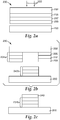
- the exemplary donor element 100 includes a donor substrate 102, and a thermal transfer layer 104.
- the donor substrate 102 can be formed from any useful material, such as a polymer film.
- a polymer film is a polyester film, for example, polyethylene terephthalate (PET) or polyethylene naphthalate (PEN) films.
- PET polyethylene terephthalate
- PEN polyethylene naphthalate
- other films with sufficient optical properties optical properties may be relevant if light is used for heating and transfer), including high transmission of light at a particular wavelength, as well as sufficient mechanical and thermal stability for the particular application, can be used.
- the donor substrate 102 in at least some instances, can be flat so that uniform coatings can be formed thereon.
- the donor substrate 102 can also typically be selected from materials that remain stable despite being heating, or heating of adjoining layers of the donor element.
- the thickness of a donor substrate can range from 0.025 mm to 0.15 mm. In an embodiment, the thickness of a donor substrate can range from 0.05 mm to 0.1 mm.
- thicker or thinner donor substrates may also be used.
- Donor elements 100 also include a thermal transfer layer 104.
- Thermal transfer layer 104 for use as disclosed herein include catalytic material.
- Catalytic materials include materials that can provide a catalytic site on a surface to make electroless deposition possible and materials that can be made to catalyze the growth of metallic materials in an electroless deposition process.
- Materials that can be made to catalyze the growth of metallic materials are often referred to as catalyst precursors.
- the catalytic material can be present in continuous or discontinuous thin films, in a colloidal dispersion (e.g. nanoparticles or inks based on metal nanoparticles such as those available from Advanced Nano Products, Korea), and catalyst precursors as discussed above.
- a catalytic material does not include a colloidal dispersion.
- Examples of materials that can catalyze the growth of metallic materials include, but are not limited to, metals such as main group metals, transition metals, noble metals, rare earth metals, and metalloids.
- group VIII B elements or group I B elements can be utilized.
- Specific metals include, but are not limited to, aluminum, scandium, titanium, vanadium, chromium, manganese, iron, cobalt, nickel, copper, zinc, gallium, germanium, yttrium, zirconium, niobium, molybdenum, technetium, ruthenium, rhodium, palladium, silver, indium, tin, antimony, lanthanum, gadolinium, hafnium, tantalum, tungsten, rhenium, osmium, iridium, platinum, gold, thallium, or combinations thereof.
- the metal, or metals are non-ferromagnetic; for example, copper, gold, iridium, palladium, platinum, rhodium, silver, rhenium, ruthenium, osmium, indium, and tin.
- one or more noble metals are utilized.
- Materials that contain one or more metals can also be used as a catalytic material.
- salts or complexes of metals such as salts of transition metals, for example salts of palladium, platinum, and silver can be utilized.
- Salts of metals can be inorganic, such as palladium chloride, or organic, such as palladium acetate or palladium propanoate.
- alkanoate salts can be utilized.
- a composition that includes a catalytic material such as a metal as exemplified above, can be utilized.
- a composition that includes metal nanoparticles, such as palladium or silver nanoparticles; or copper or nickel nanoparticles can be utilized.
- the thermal transfer layer 104 can include a vapor deposited metal, such as vapor deposited palladium.
- Catalytic materials also include materials, referred to herein as catalyst precursors that can be made to catalyze the growth of a metallic material.
- a catalyst precursor can be made to catalyze the growth of a metallic material by subjecting it to an activating condition.
- an organic material that can complex a metal such as those exemplified above can be utilized as a catalyst precursor.
- the activating condition is exposure of the catalyst precursor to a solution containing a metal for example.
- a material that, once exposed to a source of energy, can catalyze the growth of a metallic material can be utilized as a catalyst precursor.
- the activation condition is exposure to a source of energy.
- a material that, once subjected to an ion-exchange process, can catalyze the growth of a metallic material can be utilized as a catalyst precursor.
- the activating condition is exposure of the catalyst precursor to a solution that contains a metal for example that can replace an ion in the catalyst precursor.
- the activating condition can be a chemical reaction.
- a catalyst precursor that includes a metal ion, such as Pd 2+ or Ag 2+ can be exposed to a solution that will reduce the Pd2 + to Pd 0 or Ag2 + to Ag 0 .
- Exemplary reducing agents that can be utilized include, but are not limited to, tin (Sn 2+ ), formaldehyde, sodium borohydride, hydrazine, hydrazine hydrate, hydrazine sulfate, and dihydrazine sulfate.
- the thermal transfer layer 104 can include the catalyst precursor and the reducing agent.
- the thermal transfer layer could include Pd 2+ or Ag 2+ , and a reducing agent, such as Sn 2+ for example.
- the material that catalyzes the growth of the metallic material, Pd 0 or Ag 0 ) for example could then be generated in situ.
- the thermal transfer layer 104 could include Sn 2+ which could then be exposed to a solution of Pd 2+ or Ag 2+ , for example, to generate the Pd 0 or Ag 0 which catalyzes the growth of the metallic material.
- a thermal transfer layer 104 could include one layer that includes a catalyst precursor and one layer that includes a reducing agent.
- a thermal transfer layer could include a layer that includes Sn 2+ and another layer that includes Pd 2+ or Ag 2+ .
- the reduction of the Pd 2+ or Ag 2+ to Pd 0 or Ag 0 respectively, could then be accomplished by exposing the two layers to water, allowing the components to migrate to effect the reaction.
- the two layers could be transferred to the receptor surface in two separate steps. Then, once the two layers are transferred, the reaction could take place to create the catalyst.
- the reaction could be initiated by dissolution and migration of the reactive species or by thermally induced migration, or by solvent induced mobility.
- the reduction of the Pd 2+ or Ag 2+ to Pd 0 or Ag 0 respectively could then be accomplished by exposing the two layers to water, allowing the components to migrate to effect the reaction.
- the two layers could be transferred to the receptor surface in two separate steps.
- the reaction could take place to create the catalyst.
- the reaction could be initiated by dissolution and migration of the reactive species or by thermally induced migration, or by solvent induced mobility.
- a separating layer that would prevent the premature reaction of species in adjacent layers (e.g. an oxidizing and a reducing agent, an acid and a base, etc.) by acting as a chemical and/or physical barrier.
- a specific, non-limiting example of a separating layer is a solvent soluble polymer or polymer blend comprising, for example an acid functional acrylic (e.g. Elvacite 2776, Lucite International, Inc.), an amino functional acrylic (e.g.
- Molecular or ionic transport across the separating layer could be initiated before or after the laser thermal patterning step by exposing the three layered transfer stack (e.g. oxidizing layer/separating layer/reducing agent) to an aqueous solution with a controlled pH that swells the separating layer without dissolving it. This transport would allow for reaction between the two previously separate layers. Porosity of the separating layer (hence, the rate of reaction between separated layers) could also be controlled by varying its thickness, crosslink density, or phase morphology.
- Yet another class of materials that could be used as a separating layer is small molecules that readily sublime or decompose cleanly at relatively low temperature (e.g. those described in US 5,756,689 "Diazo compounds for laser-induced mass transfer imaging materials", US 5,747,217 “Laser-induced mass transfer imaging materials and methods utilizing colorless sublimable compounds", or US 5,691,098 "Laser-Induced mass transfer imaging materials utilizing diazo compounds”).
- Molecular or ionic transport across a separating layer comprising one or more of these materials could be initiated before or after the laser thermal patterning step by gradual heating of the layers. This transport would allow for reaction between the two previously separate layers. Porosity of the separating layer (hence, the rate of reaction between separated layers) could also be controlled by varying its thickness or phase morphology.
- the thermal transfer layer 104 can include a catalyst precursor and can be exposed to the source of energy either before or after at least a portion thereof is transferred to the receptor
- a material that, once exposed to a source of energy, can catalyze the growth of a metallic material can be utilized as a catalyst precursor.
- palladium acetate can be decomposed by exposure to intense UV radiation from an excimer laser to form a catalyst for electroless deposition ( J.-Y. Zhang, H. Esrom, I.W. Boyd, Applied Surface Science 96-98 (1996) 399 ).
- alumina surfaces can be activated as electroless catalysts with exposure to intense UV radiation from an excimer laser ( J.-Y. Zhang, I.W. Boyd, H. Esrom, Applied Surface Science 109-110 (1997) 253 ).
- copper acetylacetonate can be decomposed by exposure to intense UV radiation from an excimer laser to form a catalyst for electroless deposition ( J.-Y. Zhang, H. Esrom, Applied Surface Science 54 (1992) 465 ).
- a thermal transfer layer 104 as disclosed herein includes a catalytic material and can optionally include other materials.
- the other materials that may be included in the thermal transfer layer 104 are generally those that are to be included in an ultimate article or device that is to be fabricated using a method as disclosed herein.
- the thermal transfer layer 104 optionally includes another material that can contribute to the ability of the thermal transfer layer to adhere to the receptor surface and/or contribute to the ability to expose the catalytic material to the electroless deposition bath.
- the thermal transfer layer 104 can include a polymer.
- porous, swellable, or hydrogel polymeric materials can be utilized in order to easily allow the surface of the catalytic material to be at least partially exposed. Exposure of the surface of the catalytic material can be useful during electroless plating.
- the optional other material included in the thermal transfer layer 104 can include a material that is capable of being etched or dissolved away. If such a material is utilized, an additional etching or dissolution step can be utilized before the metallic material is deposited.
- the thermal transfer layer 104 can include a material that enhances the adhesion of the thermal transfer layer 104 to the receptor surface.
- the other alternative materials that contribute to the adherent nature of the thermal transfer layer 104 can be present in a separate layer of the thermal transfer layer 104 which is positioned farthest from the donor substrate so it is in contact with the receptor after transfer from the donor element to the receptor.
- polymeric binder materials can be included in the thermal transfer layer 104.
- Polymeric binder material may be UV- or thermally crosslinkable, which can then be crosslinked, to enhance adhesion, after the thermal transfer layer 104 is transferred from the donor element to the receptor surface.
- thermal transfer layers examples include, but are not limited to UV-crosslinkable materials or thermally crosslinkable materials such as those which can be crosslinked by exposure to heat or radiation, and/or by the addition of an appropriate chemical curative (e.g., H 2 O, O 2 , etc.).
- an appropriate chemical curative e.g., H 2 O, O 2 , etc.
- radiation curable materials can be utilized. Suitable materials include those listed in the Encyclopedia of Polymer Science and Engineering, Vol. 4, pp. 350-390 and 418-449 (John Wiley & Sons, 1986 ), and Vol. 11, pp. 186-212 (John Wiley & Sons, 1988).
- both insulating and conductive crosslinkable polymeric binder materials can be utilized herein.
- Insulating crosslinkable polymers as are generally known to those of skill in the art can be utilized.
- An example of an insulating crossslinkable polymer that can be utilized includes acrylates.
- Conductive crosslinkable polymers as are generally known to those of skill in the art can be utilized. Examples of conductive crosslinkable polymers include, but are not limited to, polyanilines, polyacetylenes, polyphenylenes, polyfluorenes, and poly(3,4-ethylenedioxythiophene) (PEDOT).
- PEDOT poly(3,4-ethylenedioxythiophene)
- crosslinkable materials include, but are not limited to, silane functionalized triarylamine, the poly(norbornenes) with pendant triarylamine as disclosed in Bellmann et al., Chem Mater 10, pp. 1668-1678 (1998 ), bis-functionalized hole transporting triarylamine as disclosed in Bayerl et al., Macromol. Rapid Commun. 20, pp. 224-228 (1999 ), the various crosslinked conductive polyanilines and other polymers as disclosed in U.S. Pat. No.
- thermal transfer layer may also include optional additives, including but not limited to, chelating agents (for example EDTA), coupling agents, metal adhesion promoters (for example imidazoles), coating aids (for example surfactants, dispersants, etc.) or other coating additives.
- chelating agents for example EDTA
- coupling agents for example EDTA
- metal adhesion promoters for example imidazoles
- coating aids for example surfactants, dispersants, etc.
- Other components can also be added to impart desired characteristics or desired processing advantages.
- the thermal transfer layer 104 can optionally include more than one layer.
- a thermal transfer layer that includes more than one layer can be referred to as a multicomponent transfer unit.
- These one or more layers may be formed using organic, inorganic, organometallic, and other materials.
- the transfer layer is described and illustrated as having one or more discrete layers, it will be appreciated that, at least in some instances where more than one layer is used, there may be an interfacial region that includes at least a portion of each layer. This may occur, for example, if there is mixing of the layers or diffusion of material between the layers before, during, or after transfer of the transfer layer.
- individual layers may be completely or partially mixed before, during, or after transfer of the transfer layer. This can be accomplished through the use of separation layers, as discussed above. In any case, these structures will be referred to as including more than one independent layer, particularly if different functions of a final article are to be performed by the different regions.
- One advantage of using a multicomponent transfer unit, particularly if the layers do not mix, is that the important interfacial characteristics of the layers in the multicomponent transfer unit can be produced when the thermal transfer unit is prepared and, in one embodiment, retained during transfer.
- thermal transfer layer includes a single or multicomponent transfer unit that is used to form at least part of a multilayer construction on a receptor.
- the thermal transfer layer may include all of the layers needed to form a desired construction.
- the thermal transfer layer may include fewer than all the layers needed to form a desired construction, the other layers being formed via transfer from one or more other donor elements or via some other suitable transfer or patterning method before, after, or both before and after the transfer of the thermal transfer layer.
- one or more layers of a construction may be provided on the surface of the receptor, the remaining layer or layers being included in the thermal transfer layer of one or more donor elements.
- one or more additional layers of a construction may be transferred onto the receptor after the thermal transfer layer has been patterned.
- the thermal transfer layer is used to form only a single layer of a construction.
- an exemplary thermal transfer layer includes a multicomponent transfer unit that is capable of forming at least two layers of a multilayer construction. These two layers of the multilayer construction often correspond to two layers of the thermal transfer layer.
- the thermal transfer layer may include an optional adhesive layer disposed on an outer surface of the thermal transfer layer to facilitate adhesion to the receptor.
- the adhesive layer may provide other functions as well, for example the adhesive layer may conduct electricity between the receptor and the other layers of the transfer layer or may only adhere the transfer layer to the receptor.
- the adhesive layer may be formed using, for example, thermoplastic polymers, including conducting and non-conducting polymers, conducting and non-conducting filled polymers, and/or conducting and non-conducting dispersions. Examples of suitable polymers include, but are not limited to, acrylic polymers, polyanilines, polythiophenes, poly(phenylenevinylenes), polyacetylenes, and other conductive organic materials known to one of skill in the art, having read this specification.
- Conductive adhesive layers can also include vapor or vacuum deposited organic conductors such as N,N'-bis(1-naphthyl)-N,N'-diphenylbenzidine (also known as NPB).
- An embodiment that includes a multicomponent transfer layer can optionally include a layer on the top (the layer that is farthest from the donor substrate, that will be directly on the receptor surface after transfer) that provides desired characteristics in an article after the thermal transfer layer is transferred to the receptor.
- a layer on the top the layer that is farthest from the donor substrate, that will be directly on the receptor surface after transfer
- Such a construction could be advantageous in fabricating an article in which electrical connectivity from the substrate to the metallic material is desired.
- Examples of materials that can be included in a layer such as this include, but are not limited to, conductive particles and conductive polymers.
- Such a construction could be advantageous in fabricating an article in which electrical insulation between the substrate and the metallic material is desired. Examples of materials that can be included in a layer such as this include, but are not limited to insulating poly
- the thermal transfer layer may be formed with discrete layers, it will be understood that, in at least some embodiments, the thermal transfer layer may include layers that have multiple components and/or multiple uses in the construction. It will also be understood that, at least in some embodiments, two or more discrete layers may be mixed together during transfer or otherwise combined or reacted. In any case, these layers, although mixed or combined, will be referred to as individual layers.
- the material of the adhesive layer may be present in a separate layer, in two separate layers that have mixed somewhat, or in one layer that includes the adhesive as well as the catalytic material (and other optional materials that may be present).
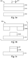
- FIG. 1b illustrates another embodiment of a donor element 120.
- This exemplary donor element 120 includes a donor substrate 122, a thermal transfer layer 124, and also includes a light to heat conversion (LTHC) layer 126 disposed between the donor substrate 122 and the thermal transfer layer 124.
- the LTHC layer 126 contains a radiation absorber that converts light energy to heat energy. The conversion of the light energy to heat energy results in the transfer of at least a portion of the thermal transfer layer 124 to a receptor (not shown).
- a LTHC layer 126 couples the energy of the light radiated from a light-emitting source into the donor element.
- a LTHC layer includes a radiation absorber that absorbs incident radiation (e.g., laser light) and converts at least a portion of the incident radiation into heat to enable transfer of the thermal transfer layer from the donor element to the receptor.
- incident radiation e.g., laser light
- the radiation absorber is disposed in another layer of the donor element, such as the donor substrate or the thermal transfer layer.
- the donor element includes an LTHC layer and also includes additional radiation absorber(s) disposed in one or more of the other layers of the donor element, such as, for example, the donor substrate or the thermal transfer layer.
- the donor element does not include an LTHC layer or radiation absorber and the thermal transfer layer is transferred using a heating element that contacts the donor element.
- the radiation absorber in the LTHC layer absorbs light in the infrared, visible, and/or ultraviolet regions of the electromagnetic spectrum.
- the radiation absorber is typically highly absorptive of the selected imaging radiation, providing an optical density at the wavelength of the imaging radiation in the range of 0.2 to 3, and in one embodiment from 0.5 to 2.
- Suitable radiation absorbing materials can include, for example, dyes (e.g., visible dyes, ultraviolet dyes, infrared dyes, fluorescent dyes, and radiation-polarizing dyes), pigments, metals, metal compounds, metal films, and other suitable absorbing materials.
- suitable radiation absorbers can include carbon black, metal oxides, and metal sulfides.
- a suitable LTHC layer can include a pigment, such as carbon black, and a binder, such as an organic polymer.
- a binder such as an organic polymer.
- Another suitable LTHC layer can include metal or metal/metal oxide formed as a thin film, for example, black aluminum (i.e., a partially oxidized aluminum having a black visual appearance).
- Metallic and metal compound films may be formed by techniques, such as, for example, sputtering and evaporative deposition. Particulate coatings may be formed using a binder and any suitable dry or wet coating techniques.
- Radiation absorber material can be uniformly disposed throughout the LTHC layer or can be non-homogeneously distributed.
- nonhomogeneous LTHC layers can be used to control temperature profiles in donor elements. This can give rise to donor elements that have higher transfer sensitivities (e.g., better fidelity between the intended transfer patterns and actual transfer patterns).
- Dyes suitable for use as radiation absorbers in an LTHC layer may be present in particulate form, dissolved in a binder material, or at least partially dispersed in a binder material
- the particle size can be, at least in some instances, about 10 ⁇ m or less, and may be about 1 ⁇ m or less.
- Suitable dyes include those dyes that absorb in the IR region of the spectrum. Examples of such dyes may be found in Matsuoka, M., "Infrared Absorbing Materials", Plenum Press, New York, 1990 ; Matsuoka, M., Absorption Spectra of Dyes for Diode Lasers, Bunshin Publishing Co., Tokyo, 1990 , U.S. Pat. Nos.
- IR absorbers marketed by Glendale Protective Technologies, Inc., Lakeland, Fla., under the designation CYASORB IR-99, IR-126 and IR-165 may also be used.
- a specific dye may be chosen based on factors such as, solubility in, and compatibility with, a specific binder and/or coating solvent, as well as the wavelength range of absorption.
- Pigmentary materials may also be used in the LTHC layer as radiation absorbers.
- suitable pigments include carbon black and graphite, as well as phthalocyanines, nickel dithiolenes, and other pigments described in U.S. Pat. Nos. 5,166,024 and 5,351,617 , incorporated herein by reference.
- black azo pigments based on copper or chromium complexes of, for example, pyrazolone yellow, dianisidine red, and nickel azo yellow can be useful.
- Inorganic pigments can also be used, including, for example, oxides and sulfides of metals such as aluminum, bismuth, tin, indium, zinc, titanium, chromium, molybdenum, tungsten, cobalt, iridium, nickel, palladium, platinum, copper, silver, gold, zirconium, iron, lead, and tellurium.
- metals such as aluminum, bismuth, tin, indium, zinc, titanium, chromium, molybdenum, tungsten, cobalt, iridium, nickel, palladium, platinum, copper, silver, gold, zirconium, iron, lead, and tellurium.
- Metal borides, carbides, nitrides, carbonitrides, bronze-structured oxides, and oxides structurally related to the bronze family e.g., WO 2.9 .
- Metal radiation absorbers may be used, either in the form of particles, as described for instance in U.S. Pat. No. 4,252,671 , incorporated herein by reference, or as films, as disclosed in U.S. Pat. No. 5,256,506 , incorporated herein by reference.
- Suitable metals include, for example, aluminum, bismuth, tin, indium, tellurium and zinc.
- a particulate radiation absorber may be disposed in a binder.
- the weight percent of the radiation absorber in the coating is generally from 1 wt-% to 30 wt-%, in an embodiment from 3 wt-% to 20 wt-%, and in another embodiment from 5 wt-% to 15 wt-%, depending on the particular radiation absorber(s) and binder(s) used in the LTHC.
- Suitable binders for use in the LTHC layer include film-forming polymers, such as, for example, phenolic resins (e.g., novolak and resole resins), polyvinyl butyral resins, polyvinyl acetates, polyvinyl acetals, polyvinylidene chlorides, polyacrylates, cellulosic ethers and esters, nitrocelluloses, and polycarbonates.
- Suitable binders may include monomers, oligomers, or polymers that have been or can be polymerized or crosslinked.
- the binder is primarily formed using a coating of crosslinkable monomers and/or oligomers with optional polymer.
- the binder includes 1 to 50 wt-%, in an embodiment, 10 to 45 wt-%, polymer (excluding the solvent when calculating wt-%).
- the monomers, oligomers, and polymers may be crosslinked to form the LTHC.
- the LTHC layer may be damaged by the heat and/or permit the transfer of a portion of the LTHC layer to the receptor with the transfer layer.
- thermoplastic resin e.g., polymer
- the binder includes 25 to 50 wt-% (excluding the solvent when calculating weight percent) thermoplastic resin, and, in one embodiment, 30 to 45 wt-% thermoplastic resin, although lower amounts of thermoplastic resin may be used (e.g., 1 to 15 wt-%).
- the thermoplastic resin is typically chosen to be compatible (i.e., form a one-phase combination) with the other materials of the binder.
- a solubility parameter can be used to indicate compatibility, as is known to one of skill in the art.
- a thermoplastic resin that has a solubility parameter in the range of 9 to 13 (cal/cm 3 ) 1/2 , in one embodiment, 9.5 to 12 (cal/cm 3 ) 1/2 , is chosen for the binder.
- suitable thermoplastic resins include polyacrylics, styrene-acrylic polymers and resins, and polyvinyl butyral.
- the LTHC layer may be coated onto the donor substrate using a variety of coating methods known in the art.
- a polymeric or organic LTHC layer is coated, in at least some instances, to a thickness of 0.05 ⁇ m to 20 ⁇ m, in one embodiment, 0.5 ⁇ m to 10 ⁇ m, and, in one embodiment, 1 ⁇ m to 7 ⁇ m.
- An inorganic LTHC layer is coated, in at least some instances, to a thickness in the range of 0.001 to 10 ⁇ m, and in one embodiment, 0.002 to 1 ⁇ m.
- FIG. 1c Another example of a donor element 130 is illustrated in FIG. 1c , and includes a donor substrate 132, an LTHC layer 136, an interlayer 138, and a thermal transfer layer 134.
- the interlayer 138 is generally disposed between the LTHC layer 136 and the thermal transfer layer 134 in donor elements in order to minimize damage and contamination of the transferred portion of the thermal transfer layer and may also reduce distortion in the transferred portion of the thermal transfer layer.
- the interlayer 138 may also influence the adhesion of the thermal transfer layer to the rest of the donor element.
- the interlayer 138 has high thermal resistance.
- the interlayer 138 does not distort or chemically decompose under the imaging conditions, particularly to an extent that renders the transferred image non-functional.
- the interlayer 138 typically remains in contact with the LTHC layer 136 during the transfer process and is not substantially transferred with the thermal transfer layer 134.
- Suitable interlayers 138 include, but are not limited to, polymer films, metal layers (e.g., vapor deposited metal layers), inorganic layers (e.g., sol-gel deposited layers and vapor deposited layers of inorganic oxides (e.g., silica, titania, and other metal oxides)), and organic/inorganic composite layers.
- Organic materials suitable as interlayer materials include, but are not limited to, both thermoset and thermoplastic materials.
- Suitable thermoset materials include, but are not limited to, resins that may be crosslinked by heat, radiation, or chemical treatment including, but not limited to, crosslinked or crosslinkable polyacrylates, polymethacrylates, polyesters, epoxies, and polyurethanes.
- the thermoset materials may be coated onto the LTHC layer 136 as, for example, thermoplastic precursors and subsequently crosslinked to form a crosslinked interlayer.
- thermoplastic materials include, for example, polyacrylates, polymethacrylates, polystyrenes, polyurethanes, polysulfones, polyesters, and polyimides. These thermoplastic organic materials may be applied via conventional coating techniques (for example, solvent coating, spray coating, or extrusion coating).
- the glass transition temperature (T g ) of thermoplastic materials suitable for use in the interlayer is about 25° C or greater, in one embodiment 50° C or greater, in one embodiment 100° C or greater, and, in another embodiment, 150° C or greater.
- the interlayer may be either transmissive, absorbing, reflective, or some combination thereof, at the imaging radiation wavelength.
- Inorganic materials suitable as interlayer materials include, for example, metals, metal oxides, metal sulfides, and inorganic carbon coatings, including those materials that are highly transmissive or reflective at the imaging light wavelength. These materials may be applied to the light-to-heat-conversion layer via conventional techniques (e.g., vacuum sputtering, vacuum evaporation, or plasma jet deposition).
- the interlayer may provide a number of benefits.
- the interlayer may be a barrier against the transfer of material from the light-to-heat conversion layer. It may also modulate the temperature attained in the transfer layer so that thermally unstable materials can be transferred.
- the presence of an interlayer may also result in improved plastic memory in the transferred material.
- the interlayer may contain additives, including, for example, photoinitiators, surfactants, pigments, plasticizers, and coating aids.
- the thickness of the interlayer may depend on factors such as, for example, the material of the interlayer, the material of the LTHC layer, the material of the transfer layer, the wavelength of the imaging radiation, and the duration of exposure of the thermal transfer element to imaging radiation.
- the thickness of the interlayer typically is in the range of 0.05 ⁇ m to 10 ⁇ m, in an embodiment, from about 0.1 ⁇ m to 4 ⁇ m, in an embodiment, 0.5 to 3 ⁇ m, and, in an embodiment, 0.8 to 2 ⁇ m.
- the thickness of the interlayer typically is in the range of 0.005 ⁇ m to 10 ⁇ m, in an embodiment, from about 0.01 ⁇ m to 3 ⁇ m, and, in an embodiment, from about 0.02 to 1 ⁇ m.
- Another suitable donor element 140 illustrated in FIG. 1d includes a donor substrate 142, an LTHC layer 146, a thermal transfer layer 144, an interlayer 148, an optional primer layer 143, and an optional release layer 145.
- Donor elements can include an optional release layer 145.
- the optional release layer 145 typically facilitates release of the thermal transfer layer 144 from the rest of the donor element (e.g., the interlayer and/or the LTHC layer) upon heating of the donor element, for example, by a light-emitting source or a heating element.
- the release layer provides some adhesion of the thermal transfer layer to the rest of the donor element prior to exposure to heat.
- Suitable release layers include, but are not limited to, conducting and non-conducting thermoplastic polymers, conducting and non-conducting filled polymers, and/or conducting and non-conducting dispersions.
- suitable polymers include acrylic polymers, polyanilines, polythiophenes, poly(phenylenevinylenes), polyacetylenes, and other conductive organic materials known to those of skill in the art.
- suitable conductive dispersions include inks containing carbon black, graphite, ultrafine particulate indium tin oxide, ultrafine antimony tin oxide, and commercially available materials from companies such as Nanophase Technologies Corporation (Burr Ridge, I11.) and Metech (Elverson, Pa.).
- suitable materials for the release layer include sublimable insulating materials and sublimable semiconducting materials (such as phthalocyanines), including, for example, the materials described in U.S. Pat. No. 5,747,217 , incorporated herein by reference.
- the optional release layer 145 may be part of the thermal transfer layer or may be a separate layer. All or a portion of the release layer may be transferred with the thermal transfer layer. Alternatively, most or substantially all of the release layer can remain with the donor substrate when the thermal transfer layer is transferred. In some instances, for example with a release layer that includes a sublimable material, a portion of the release layer may be dissipated during the transfer process.
- the materials used to form the donor substrate 142 and the LTHC layer 146 are selected to improve adhesion between the LTHC layer 146 and the donor substrate 142.
- An optional priming layer 143 can be used to increase uniformity during the coating of subsequent layers and also increase the interlayer bonding strength between the LTHC layer 146 and the donor substrate 142.
- a suitable substrate with an optional primer layer is available from Teijin Ltd. (Product No. HPE100, Osaka, Japan).
- Materials can be coated onto donor substrates to form the thermal transfer layers of the donor elements.
- the thermal transfer layer materials can then be patterned via selective thermal transfer from the donor to a receptor.
- Coating onto a donor followed by patterning via selective transfer represents a de-coupling of layer coating steps from patterning steps.
- An advantage of de-coupling coating and patterning steps is that materials can be patterned on top of or next to other materials that would be difficult to pattern, if possible at all, using conventional patterning processes.
- a solvent-coated layer can be patterned on top of a solvent-susceptible material that would be dissolved, attacked, penetrated, and/or rendered inoperable for its intended purpose in the presence of the solvent had the solvent-coated layer been coated directly on the solvent-susceptible material.
- a thermal transfer layer of a donor element can be made by solvent-coating a first material on the donor, suitably drying the coating, and then depositing a second layer that includes material that may be susceptible to the solvent used to coat the first material. Damage to the second layer can be minimized or eliminated by evaporation, or otherwise removal, of much or most of the solvent before coating of the second layer.
- the second layer Upon thermal transfer of this multicomponent thermal transfer layer from the donor element to a receptor, the second layer becomes positioned between the receptor and the solvent-coated first material. Thermal transfer of multiple layer units results in a reverse ordering of the transferred layers on the receptor relative to the ordering on the donor element. Because of this, solvent-susceptible layers can be patterned underneath solvent-coated layers.
- the solvent-susceptible material(s) can be patterned by any suitable method, including thermal transfer from a donor element, followed by another thermal transfer step using another donor to transfer the solvent-coated material(s). The same holds for patterned thermal transfer of solvent-coated materials next to, but not necessarily in contact with, materials or layers on a receptor that may be incompatible with the solvent.
- FIG. 2a illustrates the step of placing a donor element 230, discussed above, proximate the surface of a receptor 200.
- This illustrative donor element 230 includes a donor substrate 232, and a thermal transfer layer 234, which is made up of a release layer 235, a catalytic layer 237 (a layer that includes the catalytic material), and a polymer layer 233 (a layer that includes a polymeric binder material).
- the catalytic layer 237 and the polymer layer 233 can be one homogeneous layer.
- the donor element is brought into contact with the receptor surface.
- the donor element and receptor are configured so that the thermal transfer layer of the donor element is placed proximate the surface of the receptor.
- pressure or vacuum can be used to hold the donor element in intimate contact with the receptor surface.
- the receptor to which the donor element can be transferred can include any material which the thermal transfer layer can adhere to or can be made to adhere to.
- the particular receptor that will be utilized can depend at least in part on the article that is being fabricated using a method disclosed herein.
- Examples of receptors include, but are not limited to any useful material, such as a polymer film, glass, or metal.
- One suitable type of polymer film is a polyester film, for example, PET or PEN films.
- glass is the receptor.
- the receptor comprises glass or polymer as a support for electrical or electronic circuitry such as a flat panel display backplane, or elements thereof.
- Exemplary receptors that can be utilized can be conditioned or treated prior to thermal transfer of the thermal transfer layer.
- the conditioning could include cleaning treatments such as exposure to a plasma or a reactive chemical such as ozone or an organic peroxide.
- the treatment could also optionally include chemical surface modification with, for example, a silane coupling agent or a surfactant.
- the thermal transfer layer of the donor element is thermally transferred to the receptor.
- the arrows 250 in FIG. 2a schematically illustrate the application of thermal energy, which transfers at least a portion of the donor element 230 to the receptor 200.
- the energy, which is applied to at least a portion of the donor element 230, functions to transfer the portion of the thermal transfer layer 234 which is exposed to the energy.
- a variety of radiation-emitting sources can be used in the disclosed methods.
- the transfer is accomplished with a laser.
- high-powered light sources e.g., xenon flash lamps and lasers
- infrared, visible, and ultraviolet lasers can be particularly useful.
- Suitable lasers include, for example, high power (e.g. ⁇ 100 mW) single mode laser diodes, fiber-coupled laser diodes, and diode-pumped solid state lasers (e.g., Nd:YAG and Nd:YLF).
- Laser exposure dwell times can be in the range from, for example, about 0.1 to 100 microseconds and laser fluxes can be in the range from, for example, about 0.01 to about 1 J/cm 2 .
- a laser can be particularly useful as the radiation source.
- Laser sources are compatible with both large rigid substrates such as 1 m x 1 m x 1 mm glass, and continuous or sheeted film substrates, such as 100 ⁇ m polyimide sheets.
- Resistive thermal print heads or arrays may be used, for example, with simplified donor element constructions that do not include an LTHC layer and radiation absorber. This may be particularly useful with smaller substrate sizes (e.g., less than approximately 30 cm in any dimension) or for larger patterns, such as those required for alphanumeric segmented displays.
- a radiation source can generally be used to heat the LTHC layer (and/or other layer(s) containing radiation absorber) in an imagewise fashion (e.g., digitally or by analog exposure through a mask) to perform imagewise transfer of the thermal transfer layer from the donor element to the receptor according to a pattern.
- imagewise fashion e.g., digitally or by analog exposure through a mask
- a heating element such as a resistive heating element, may be used to transfer the thermal transfer layer.
- the donor element can be selectively contacted with the heating element to cause thermal transfer of a portion of the thermal transfer layer according to a pattern.
- the donor element may include a layer that can convert an electrical current applied to the layer into heat.
- the thermal transfer layer is transferred to the receptor without transferring any of the other layers of the donor element, such as the optional interlayer and the LTHC layer.
- the presence of the optional interlayer may eliminate or reduce the transfer of the LTHC layer to the receptor and/or reduce distortion in the transferred portion of the thermal transfer layer.
- the adhesion of the interlayer to the LTHC layer is greater than the adhesion of the interlayer to the thermal transfer layer.
- a reflective or an absorptive interlayer can be used to attenuate the level of imaging radiation transmitted through the interlayer and reduce any damage to the transferred portion of the thermal transfer layer that may result from interaction of the transmitted radiation with the thermal transfer layer and/or the receptor. This can be particularly beneficial in reducing thermal damage which may occur when the receptor is highly absorptive of the imaging radiation.
- Large donor elements can be used, including donor elements that have length and width dimensions of a meter or more.
- a laser can be rastered or otherwise moved across the large donor element, the laser being selectively operated to illuminate portions of the donor element according to a desired pattern.
- the laser may be stationary and the donor element moved beneath the laser.
- Materials can be patterned onto receptors by selective thermal transfer of the materials from one or more donor elements.
- a donor element can be heated by application of directed heat on a selected portion of the donor element. Heat can be generated using a heating element (e.g., a resistive heating element), converting radiation (e.g., a beam of light) to heat, and/or applying an electrical current to a layer of the donor element to generate heat.
- a heating element e.g., a resistive heating element
- converting radiation e.g., a beam of light
- an electrical current to a layer of the donor element to generate heat.
- thermal transfer using light from, for example, a lamp or laser can be advantageous because of the accuracy and precision that can often be achieved.
- the size and shape of the transferred pattern (e.g., a line, circle, square, or other shape) can be controlled by, for example, selecting the size of the light beam, the exposure pattern of the light beam, the duration of directed beam contact with the donor element, and the materials of the donor element.
- Thermal transfer using light can often provide better accuracy and quality control for very small devices, such as small optical and electronic devices, including, for example, transistors and other components of integrated circuits, as well as components for use in a display, such as electroluminescent lamps and control circuitry. Moreover, thermal transfer using light may, at least in some instances, provide for better registration when forming multiple devices over an area that is large compared to the device size. As an example, components of a display, which has many pixels, can be formed using this method.
- multiple donor elements may be used to form a device or other object, or to form adjacent devices, other objects, or portions thereof.
- the multiple donor elements may include donor elements with multicomponent thermal transfer units and donor elements that transfer a single thermal transfer layer.
- a device or other object may be formed using one or more donor elements with multicomponent thermal transfer units and/or one or more donor elements that each can be used to transfer a single layer or a multilayer unit.
- Thermal transfer of one or more layers to form a device or an array of devices can also be useful, for example, to reduce or eliminate wet processing steps of processes such as photolithographic patterning, which are used to form many electronic and optical devices.
- Thermal transfer to pattern layers from donor elements can also be useful to de-couple layer coating steps from patterning steps, for example where such coupling can limit the types of layered structures, or the types of adjacent structures, that can be patterned.
- conventional patterning processes such as photolithography, ink-jet, screen printing, and various mask-based techniques
- layers are typically coated directly onto the substrate on which patterning occurs. Patterning can take place simultaneously with coating (as for ink-jet, screen printing, and some mask-based processes) or subsequent to coating via etching or another removal technique.
- a difficulty with such conventional approaches is that solvents used to coat materials, and/or etching processes used to pattern materials, can damage, dissolve, penetrate, and/or render inoperable previously coated or patterned layers or materials.
- FIG. 2b shows the donor element 230 and the receptor 200 after the donor element 230 has been exposed to energy.
- the portion of the donor element 230 that was exposed to the thermal energy is transferred to the receptor, i.e., the transferred portion 234b of the thermal transfer layer.
- the portion of the donor element 230 which was not exposed to the thermal energy maintains the thermal transfer layer on the donor substrate 232, i.e., the remaining portion 234a of the thermal transfer layer.
- the catalyst precursor in an embodiment that includes a catalyst precursor, can be converted to an active catalyst before, during, or after at least a portion of the thermal transfer layer is transferred to the receptor.
- the activating condition can be carried out before, during or after the thermal transfer step.
- the activating condition can occur during the thermal transfer of the thermal transfer layer.
- the catalyst precursor in an embodiment that includes a thermally activatable catalyst precursor, can be activated before or after the thermal transfer of the thermal transfer layer.
- the catalyst precursor can be thermally treated to form nanoparticles before or after the thermal transfer layer is transferred.
- catalyst precursors can be activated by energy from a number of sources, including but not limited to, argon ion lasers, excimer lasers, Nd:YAG lasers, and synchrotron systems.
- sources including but not limited to, argon ion lasers, excimer lasers, Nd:YAG lasers, and synchrotron systems.
- having chosen a particular catalyst precursor would know the type of energy source, and the particular functional details of using that energy source.
- the next step in methods disclosed herein is to electrolessly deposit a metallic material on the receptor by growth of the metallic material on the catalytic material.
- Fig. 2c illustrates this exemplary article after the metallic material 242 has been deposited on the transferred portion 234b of the thermal transfer layer.
- the catalytic material is a catalyst precursor
- the catalyst precursor can be converted to an active catalyst before or during the electroless deposition step.
- the patterned receptor surface could be placed in an electroless deposition bath that includes a reducing agent.
- electroless deposition refers to a process for the electroless plating of metals. It typically involves the use of an electroless plating solution that contains a soluble form of the deposit metal together with a reducing agent.
- the soluble form of the deposit metal is usually an ionic species or a metal complex (i.e., a metal species coordinated to one or more ligands).
- electroless deposition does not include the application of electrical current to a work piece that is being coated. Once the thermal transfer layer including the catalytic material is thermally transferred from the donor element to the receptor surface, the receptor can be immersed in an appropriate plating bath.
- the catalytic material or an activated version of the catalytic material (in the case of a catalyst precursor) catalyzes the deposition of the deposit metal from the plating solution.
- plating proceeds by the continued reduction of the solution metal source, catalyzed by its own metal surface, hence the term "autocatalytic.”
- electroless deposition can involve displacement reactions.
- a first metal is immersed in a solution of metal salts of a second metal with a partial attack on the surface of the first metal and the simultaneous spontaneous deposition of the second metal at its surface.
- the first metal functions as the reducing agent, and is also referred to herein, when the term "catalytic material" is utilized.
- Metallic materials that can be formed using electroless deposition include copper, nickel, gold, silver, palladium, rhodium, ruthenium, tin, cobalt, as well as alloys of these metals with each other or with phosphorous or boron, as well as compounds of these metals with each other or with phosphorous or boron.
- zinc can be formed using electroless plating via a displacement mechanism instead of a autocatalysis mechanism.
- the metallic deposit metal includes copper, silver, gold, platinum, palladium, or some combination thereof.
- the deposit metal and the catalytic material can be the same or different.
- the catalytic material is a catalytic precursor that has to be reduced in order to catalyze electroless deposition
- such reduction can occur separate from the catalytic growth of the deposit metal or coincident with the catalytic growth of the metallic deposit.
- Processes where the catalytic material is reduced separate from the catalytic growth may provide an advantage in that it can occur at a faster rate, allowing for processing advantages.
- the catalytic material can be reduced by photo-reduction, chemical reduction, heat reduction, or e-beam reduction.
- suitable reducing agents include, but are not limited to, formaldehyde, hydrazine, borohydrides, aminoboranes, and hypophosphite.
- FIGs. 3a-3C depict another exemplary embodiment of a donor element 300 and a receptor 310.
- This exemplary donor element 300 includes at least a donor substrate 302 and a thermal transfer layer 304.
- This exemplary thermal transfer layer 304 generally includes the catalytic material.
- the arrows 350 in FIG. 3a schematically illustrate the energy that transfers at least a portion of the thermal transfer layer 304 to the receptor 310.
- FIG. 3b after exposure of the donor element 300 to the energy, there is a transferred portion 304b of the thermal transfer layer on the receptor 310 and a remaining portion 304a of the thermal transfer layer 304 on the donor substrate 302.
- FIG. 3c illustrates the article after the metallic material 322 is deposited on the transferred portion 304b of the thermal transfer layer.
- FIG. 4 illustrates one exemplary method generally utilizing the steps disclosed herein.
- donor element that includes a thermal transfer layer having a catalytic material, more specifically an active catalyst
- the transferred portion of the thermal transfer layer is exposed to electroless plating (step 420) to deposit the metallic material on the transferred portion of the thermal transfer layer, thereby creating an article having a patterned metallic material.
- FIG. 4 also illustrates an optional step 430 of curing a carrier polymer that is included in the thermal transfer layer. The optional curing creates a cured thermal transfer layer on the receptor.
- FIG. 5 illustrates another exemplary method generally utilizing the steps disclosed herein.
- This exemplary method demonstrates the production of the donor element by coating a donor stock film with a catalyst precursor (step 400) to create a donor element with a catalyst precursor.
- a donor stock film can include a donor substrate, a LTHC layer, and an interlayer.
- the donor element including the catalyst precursor can then either have the catalyst precursor converted to the catalyst, step 410; or can have at least a portion of the thermal transfer layer transferred to the receptor, step 405. If the catalyst precursor is first converted, the thermal transfer can then be transferred to the receptor, step 405; or alternatively, if the thermal transfer layer was transferred first, the catalyst precursor can then be converted to an active catalyst; step 410. Either way, the next step is to electrolessly plate the metallic material, step 420, to create an article having a patterned metallic material.
- FIG. 6 illustrates another exemplary embodiment of a method that includes an optional step of etching 440 to more fully exposed the catalytic material to the electroless plating solution.
- etching 440 to more fully exposed the catalytic material to the electroless plating solution.
- One of skill in the art can easily determine, based at least in part, on the particular polymeric binder how the catalytic material can be exposed.
- Articles that can be fabricated using the disclosed methods generally have patterned portions of the thermal transfer layer that are covered with metallic materials.
- the patterned portions of the thermal transfer layer covered with the metallic materials i.e. the metallic coating
- the overall features are referred to as the overall features.
- the portions of the thermal transfer layer and the metallic materials, i.e., the overall features can be of any size.
- the size of the overall features includes both the height of the patterned thermal transfer layer and the height of the metallic materials. Given this, the size of the overall features can be about 1 micrometer ( ⁇ m) or larger in width, and about 20 nanometers (nm) or larger in height.
- the size of the patterned portions of the thermal transfer layer can be about 1 ⁇ m or larger in width and about 20 nm or larger in height.
- the depth of the metallic materials on the patterned portions of the thermal transfer layer is about 1 angstrom ( ⁇ ) or greater.
- ⁇ angstrom
- Exemplary articles described and formed herein can have grids of metallic material, and such articles can be used for example, for electromagnetic interference (EMI) shielding.
- Exemplary articles described and formed herein can have traces of metallic material, and such articles can be used for example, for touch screens, for sensor applications, for circuits, to make reflective indicia, or to create fluid flow devices (where the patterned metallic deposits can be hydrophilic and the non-patterned portions are hydrophobic).
- An exemplary article that could be formed using methods disclosed herein are flat panel display backplanes including multiple display backplanes on a mother glass, which includes copper or other conductive metal bus lines.
- Exemplary articles described and formed herein can have repeating dots or islands of metallic material, and such articles can be used for example, to create shielding effects.
- the articles include patterns of metallic deposits that can be used to conduct an electric current.
- Exemplary articles described and formed herein can have reflective or semitransparent layers of metallic material, and such articles can be used for example, in microelectromechanical (MEMs) or microelectrooptical devices.
- Exemplary articles that can be formed using methods disclosed herein include micromirror arrays.
- Exemplary articles that are described and formed herein can advantageously have the receptor, the portion of the thermal transfer layer, the metallic material, or some combination thereof matched so that thermal expansion properties of the overall article are similar. It will also be understood by one of skill in the art that once an article has been formed using a method as disclosed herein, further processing steps can be carried out on that article without deviating from the scope of this disclosure.
- a donor stock film (donor substrate, LTHC layer, and interlayer) was prepared in the following manner.
- An LTHC solution (Table 1) was coated onto a polyethylene terephthalate (PET) film (M7Q, 2.88 mil, DuPont Teijin Films, Hopewell VA).
- the LTHC solution was applied with a laboratory microgravure coater (model CAG-150, Yasui Seiki, Kanagawa, Japan) to achieve a dry thickness of approximately 2.7 microns.
- the coating was in-line dried and cured under ultraviolet (UV) radiation.
- the cured coating had an optical density of approximately 1.18 when measured using incident light having a wavelength of 1064 nm.
- the sample 1 donor element was prepared in the following manner.
- a donor stock film comprising both LTHC and IL as described above was vacuum coated with 100 ⁇ of copper phthalocyanine (CuPC) using a standard thermal evaporation procedure in a Balzers vacuum chamber at a background pressure of 10 -7 Torr.
- the donor was then coated with 10 ⁇ of palladium metal at a rate of 2 ⁇ /sec using an e-beam deposition system.
- CuPC copper phthalocyanine
- the CuPC was then overcoated with a solution of 5 wt% polystyrene (MW 50K, Polysciences Inc., Warrington, PA)/poly(styrene-co-methyl methacrylate) (Aldrich, Milwaukee, WI) in toluene using a #3 Mayer rod in order to achieve a dry thickness of approximately 200 nm.
- the donor was then baked at 100 °C for 10 minutes in a nitrogen purged oven.
- the sample 2 donor element was prepared in the following manner.
- a donor stock film comprising both LTHC and IL as described above was vacuum coated with 100 ⁇ of copper phthalocyanine (CuPC) using a standard thermal evaporation procedure in a Balzers vacuum chamber at a background pressure of 10 -7 Torr.
- the donor was then coated with 10 ⁇ of palladium metal at a rate of 2 ⁇ /sec.
- the custom built e-beam deposition system was made by Kurt Lesker, Inc.
- the CuPC was then overcoated with a solution with a UV curable solution (Table 5) using a #3 Mayer rod in order to achieve a dry thickness of approximately 200 nm.
- the donor was then baked at 100 °C for 10 minutes in a nitrogen purged oven. Table 5.
- UV Curable Polymer Solution Trade Name Supplier Wt% solution Wt% solids Elvacite 4026 Lucite International 37.74 4.62 Sartomer SR351HP Sartomer 42.45 5.20 Sartomer CN975 Sartomer 14.15 1.73 Irgacure 369 Ciba Specialty Chemicals 5.66 0.69 2-Butanone (MEK) 87.76 100 100
- the imaged sample was baked at 100 °C for 10 minutes in a nitrogen purged oven then cured using a Light Hammer UV curing system from Fusion UV Systems Inc. The sample was exposed four times to UV irradiation by passage under a D bulb at 100% power at 20 ft/min.
- the sample 3 donor element was prepared in the following manner.
- a donor stock film comprising both LTHC and Interlayer and described above was coated with a UV curable polymer binder (Table 6) containing palladium nanoparticles.
- Table 6 UV Curable Polymer Solution with Palladium Nanoparticles Trade Name Supplier Wt% solution Wt% solids Elvacite 4026 Lucite International 33.90 4.56 Sartomer SR351HP Sartomer 38.14 5.13 Sartomer CN975 Sartomer 12.71 1.71 Irgacure 369 Ciba Specialty Chemicals 5.08 0.68 Pd NP Johnson Matthey 10.17 1.37 2-Butanone (MEK) 86.56 100 100
- the solution was coated using a #3 Mayer Rod to give an approximately dry thickness of 200nm.
- the donor was then baked at 100 °C for 10 minutes in a nitrogen purged oven.
- the imaged sample was baked at 200 °C for 20 minutes in a nitrogen purged oven then cured using a Light Hammer UV curing system from Fusion UV Systems Inc. The sample was exposed four times to UV irradiation by passage under a D bulb at 100% power at 10 ft/min. The imaged sample was then Ar plasma treated at 100W power for 1 minute to expose the Pd nanoparticles.
- the sample 4 donor element was prepared in the following manner.
- a donor stock film comprising both LTHC and Interlayer and described above was coated with a UV curable polymer binder (Table 7) containing palladium acetate.
- the solution was coated using a #3 Mayer Rod to give an approximately dry thickness of 200nm.
- the donor was then baked at 100 °C for 10 minutes in a nitrogen purged oven. Table 7.
- the imaged sample was baked at 200 °C for 20 minutes in a nitrogen purged oven then cured using a Light Hammer UV curing system from Fusion UV Systems Inc. The sample was exposed four times to UV irradiation by passage under a D bulb at 100% power at 10 ft/min.
- Sample number 1 was laminated onto a piece of 0.7 mm thick glass substrate that had been surface treated with Argon plasma from Plasma Science.
- the Argon plasma treatment was done at 100W power for 1 minute.
- Laser imaging was performed by exposing the donor film in a laser imaging system based on a single-mode Nd:YAG laser with a power of 1 watt at the film plane.
- the laser beam was scanned across the substrate using a system of linear galvanometers, with the laser beam focused onto the image plane using an f-theta scan lens as part of a near-telecentric configuration.
- the laser spot size, measured at 1/e 2 intensity was 18 x 250 microns.
- the beam was scanned unidirectionally with a triangle dither pattern oscillating at a frequency of 400 KHz. Nominal linewidth was set to 110 microns with a pitch of 165 microns.
- Sample numbers 2, 3, and 4 were laminated onto a piece of 0.7 mm thick glass substrate or in case of sample 2, a piece of PET film that had been surface treated with Argon plasma from Plasma Science.
- the Argon plasma treatment was done at 100W power for 1 minute.
- Laser imaging was performed by exposing the donor film to a mask based imaging system with a laser operating at 808nm continuous wave mode.
- the laser spot size was 100 x 100 microns.
- Nominal linewidth was set to 100 microns with a pitch of 165 microns.
- Electroless Plating Solution Trade Name Supplier Concentration Copper sulfate pentahydrate Alfa Aesar 5g/L Sodium potassium tartrate Fisher Scientific 25g/L Sodium hydroxide EMD 7g/L Formaldehyde, 37% solution Alfa Aesar 10g/L
Description
- This disclosure is related to the formation of a metallic material on a substrate.
- Formation of small scale, high-resolution features is an ever moving target for the advancement of manufacturing processes. Conductive traces for printed wiring boards (PWBs) is an exemplary application for such processes. Electroless deposition is a plating method that is used for the fabrication of such features. The chemistry and process of electroless deposition has been established for quite some time, and is generally commercially available. There remains however, a need for advancements in selectively applying the catalytic material to the substrate that is eventually subjected to electroless deposition processes.
-
AU 676 356 B2 -
WO 2005/053368 A1 discloses method of forming a metal pattern and a metal pattern obtained by the method. The method may include the steps of forming on a substrate a polymer layer in which a polymer having a functional group that interacts with an electroless plating catalyst or a precursor thereof is chemically bonded directly to the substrate in a pattern form, adding the electroless plating catalyst or precursor thereof to the polymer layer, and forming a metal layer in the pattern form by electroless plating. -
WO 2006/045084 A1 discloses a donor element useful in an assemblage for imaging by exposure to light. The donor element comprises a support layer, a light-to-heat conversion layer disposed adjacent the support layer containing a light absorber, and a transfer layer disposed adjacent the light-to-heat conversion layer opposite the support layer. The donor element also includes a release-modifier disposed between the support layer and the transfer layer. - A method and an article as defined by the independent claims are provided. The dependent claims define embodiments.
- A method of forming a metallic material on a receptor that includes the steps of: placing a donor element proximate a receptor, wherein the donor element includes a donor substrate and a thermal transfer layer, wherein the thermal transfer layer includes a catalytic material, and wherein the thermal transfer layer of the donor element is placed proximate the surface of the receptor; thermally transferring at least a portion of the thermal transfer layer from the donor element to the receptor; and electrolessly depositing a metallic material on the receptor by growth of the metallic material on the catalytic material.
- An article including, in the following order: a receptor substrate; a patterned first layer, wherein the first layer is capable of adhering to the receptor substrate; a patterned second layer including a catalytic material; and an electrolessly deposited metallic material, wherein the metallic material has the same pattern as the patterned first layer and the second patterned layer, wherein the patterned first layer and the patterned second layer are thermally transferred to the receptor substrate from a donor element and would be incompatible if originally formed on the receptor substrate in the order in which they are found on the receptor substrate.
- A thermal transfer donor element including, in the following order: a donor substrate; a light-to-heat conversion layer; and a thermal transfer layer that includes a catalytic material.
-
-
FIG. 1a is a schematic cross section of one example of a donor element as disclosed herein. -
FIG. 1b is a schematic cross section of one example of a donor element as disclosed herein. -
FIG. 1c is a schematic cross section of one example of a donor element as disclosed herein. -
FIG. 1d is a schematic cross section of one example of a donor element as disclosed herein. -
FIGs. 2a - 2c are schematic cross sections illustrating at least a portion of a donor element having a donor substrate, a light to heat conversion (LTHC) layer, an interlayer, and a thermal transfer layer being transferred to the surface of a receptor. -
FIGs. 3a - 3c are schematic cross sections illustrating at least a portion of a donor element having a thermal transfer layer being transferred to the surface of a receptor. -
FIG. 4 illustrates an exemplary method of forming a patterned metallic material. -
FIG. 5 illustrates an exemplary method of forming a patterned metallic material. -
FIG. 6 illustrates an exemplary method of forming a patterned metallic material. -
FIG. 7 is a micrograph of a sample. - It is to be understood that embodiments beyond what are mentioned here are contemplated and may be made without departing from the scope of the claims. The following detailed description, therefore, is not to be taken in a limiting sense.
- All scientific and technical terms used herein have meanings commonly used in the art unless otherwise specified. The definitions provided herein are to facilitate understanding of certain terms used frequently herein and are not meant to limit the scope of the present disclosure.
- Unless otherwise indicated, all numbers expressing feature sizes, amounts, and physical properties used in the specification and claims are to be understood as being modified in all instances by the term "about." Accordingly, unless indicated to the contrary, the numerical parameters set forth in the foregoing specification and attached claims are approximations that can vary depending upon the desired properties sought to be obtained by those skilled in the art utilizing the teachings disclosed herein.
- The recitation of numerical ranges by endpoints includes all numbers subsumed within that range (e.g. 1 to 5 includes 1, 1.5, 2, 2.75, 3, 3.80, 4, and 5) and any range within that range.
- As used in this specification and the appended claims, the singular forms "a", "an", and "the" encompass embodiments having plural referents, unless the content clearly dictates otherwise. As used in this specification and the appended claims, the term "or" is generally employed in its sense including "and/or" unless the content clearly dictates otherwise.
- Disclosed herein is a method of forming a metallic material on a receptor surface including the steps of: placing a donor element proximate a receptor surface, wherein the donor element includes a donor substrate and a thermal transfer layer, wherein the thermal transfer layer includes a catalytic material, and wherein the thermal transfer layer of the donor element is placed proximate the receptor surface; thermally transferring at least a portion of the thermal transfer layer from the donor element to the receptor surface; and electrolessly depositing a metallic material on the receptor surface by growth of the metallic material on the catalytic material.
- Methods disclosed herein offer a process for the electroless plating of metals. In an embodiment, it can involve the use of an electroless plating solution that contains a soluble form of the deposit metal together with a reducing agent. The soluble form of the deposit metal is usually an ionic species or a metal complex (i.e., a metal species coordinated to one or more ligands). Generally, the process does not include the application of electrical current to a work piece that is being coated. The process generally utilizes a catalytic surface. Once the deposition begins at the catalytic surface, plating proceeds by the continued reduction of the solution metal source, catalyzed by its own metal surface, hence the term "autocatalytic." In embodiments of the method, the catalytic surface can be provided by a catalytic material, such as a noble metal seed layer, or by reducing a catalyst precursor, such as the salt of a noble metal, to form such a layer.
- Methods that are disclosed herein utilize principles and materials that are associated with Laser Induced Thermal Imaging (LITI). Further details regarding LITI donor films, and methods of utilizing them can be found in
U.S. Patent Nos. 6,866,979 ;6,586,153 ;6,468,715 ;6,284,425 ;6,194,119 ; and5,725,989 , all of which are incorporated herein by reference thereto. LITI is generally a dry, digital patterning method in which a thin film coating is selectively transferred from a donor, across a space, to a receptor. The areas of the donor that are exposed to a source of thermal energy are transferred to the receptor. - One example of a
donor element 100 is illustrated inFIG. 1a . Theexemplary donor element 100 includes adonor substrate 102, and athermal transfer layer 104. - The
donor substrate 102 can be formed from any useful material, such as a polymer film. One suitable type of polymer film is a polyester film, for example, polyethylene terephthalate (PET) or polyethylene naphthalate (PEN) films. However, other films with sufficient optical properties (optical properties may be relevant if light is used for heating and transfer), including high transmission of light at a particular wavelength, as well as sufficient mechanical and thermal stability for the particular application, can be used. Thedonor substrate 102, in at least some instances, can be flat so that uniform coatings can be formed thereon. Thedonor substrate 102 can also typically be selected from materials that remain stable despite being heating, or heating of adjoining layers of the donor element. In an embodiment, the thickness of a donor substrate can range from 0.025 mm to 0.15 mm. In an embodiment, the thickness of a donor substrate can range from 0.05 mm to 0.1 mm. One of skill in the art will also understand that thicker or thinner donor substrates may also be used. -
Donor elements 100 also include athermal transfer layer 104.Thermal transfer layer 104 for use as disclosed herein include catalytic material. Catalytic materials include materials that can provide a catalytic site on a surface to make electroless deposition possible and materials that can be made to catalyze the growth of metallic materials in an electroless deposition process. For example, compounds that can be made to catalyze the growth of metallic materials by a reduction reaction to form an active catalytic material. Materials that can be made to catalyze the growth of metallic materials are often referred to as catalyst precursors. Generally, the catalytic material can be present in continuous or discontinuous thin films, in a colloidal dispersion (e.g. nanoparticles or inks based on metal nanoparticles such as those available from Advanced Nano Products, Korea), and catalyst precursors as discussed above. In one embodiment, a catalytic material does not include a colloidal dispersion. - Examples of materials that can catalyze the growth of metallic materials include, but are not limited to, metals such as main group metals, transition metals, noble metals, rare earth metals, and metalloids. In an embodiment, group VIII B elements or group I B elements can be utilized. Specific metals include, but are not limited to, aluminum, scandium, titanium, vanadium, chromium, manganese, iron, cobalt, nickel, copper, zinc, gallium, germanium, yttrium, zirconium, niobium, molybdenum, technetium, ruthenium, rhodium, palladium, silver, indium, tin, antimony, lanthanum, gadolinium, hafnium, tantalum, tungsten, rhenium, osmium, iridium, platinum, gold, thallium, or combinations thereof. In an embodiment, the metal, or metals are non-ferromagnetic; for example, copper, gold, iridium, palladium, platinum, rhodium, silver, rhenium, ruthenium, osmium, indium, and tin. In an embodiment, one or more noble metals are utilized. Materials that contain one or more metals can also be used as a catalytic material. For example, salts or complexes of metals, such as salts of transition metals, for example salts of palladium, platinum, and silver can be utilized. Salts of metals can be inorganic, such as palladium chloride, or organic, such as palladium acetate or palladium propanoate. In an embodiment, alkanoate salts can be utilized.
- In an embodiment, a composition that includes a catalytic material, such as a metal as exemplified above, can be utilized. For example, a composition that includes metal nanoparticles, such as palladium or silver nanoparticles; or copper or nickel nanoparticles can be utilized. In an embodiment, the
thermal transfer layer 104 can include a vapor deposited metal, such as vapor deposited palladium. - Catalytic materials also include materials, referred to herein as catalyst precursors that can be made to catalyze the growth of a metallic material. In an embodiment, a catalyst precursor can be made to catalyze the growth of a metallic material by subjecting it to an activating condition. In an embodiment, for example, an organic material that can complex a metal, such as those exemplified above can be utilized as a catalyst precursor. In such an embodiment, the activating condition is exposure of the catalyst precursor to a solution containing a metal for example. In an embodiment, for example, a material that, once exposed to a source of energy, can catalyze the growth of a metallic material can be utilized as a catalyst precursor. In such an embodiment, the activation condition is exposure to a source of energy. In an embodiment, for example, a material that, once subjected to an ion-exchange process, can catalyze the growth of a metallic material can be utilized as a catalyst precursor. In such an embodiment, the activating condition is exposure of the catalyst precursor to a solution that contains a metal for example that can replace an ion in the catalyst precursor.
- In an embodiment, the activating condition can be a chemical reaction. For example, a catalyst precursor that includes a metal ion, such as Pd2+ or Ag2+, can be exposed to a solution that will reduce the Pd2+ to Pd0 or Ag2+ to Ag0. Exemplary reducing agents that can be utilized include, but are not limited to, tin (Sn2+), formaldehyde, sodium borohydride, hydrazine, hydrazine hydrate, hydrazine sulfate, and dihydrazine sulfate.
- In an embodiment where the catalyst precursor is reduced to form an active catalyst, the
thermal transfer layer 104 can include the catalyst precursor and the reducing agent. For example, the thermal transfer layer could include Pd2+ or Ag2+, and a reducing agent, such as Sn2+ for example. The material that catalyzes the growth of the metallic material, Pd0 or Ag0) for example could then be generated in situ. Alternatively, thethermal transfer layer 104 could include Sn2+ which could then be exposed to a solution of Pd2+ or Ag2+, for example, to generate the Pd0 or Ag0 which catalyzes the growth of the metallic material. Alternatively, athermal transfer layer 104 could include one layer that includes a catalyst precursor and one layer that includes a reducing agent. For example, a thermal transfer layer could include a layer that includes Sn2+ and another layer that includes Pd2+ or Ag2+. The reduction of the Pd2+ or Ag2+ to Pd0 or Ag0 respectively, could then be accomplished by exposing the two layers to water, allowing the components to migrate to effect the reaction. In a similar fashion, the two layers could be transferred to the receptor surface in two separate steps. Then, once the two layers are transferred, the reaction could take place to create the catalyst. For example, the reaction could be initiated by dissolution and migration of the reactive species or by thermally induced migration, or by solvent induced mobility. - The reduction of the Pd2+ or Ag2+ to Pd0 or Ag0 respectively, could then be accomplished by exposing the two layers to water, allowing the components to migrate to effect the reaction. In a similar fashion, the two layers could be transferred to the receptor surface in two separate steps. Then, once the two layers are transferred, the reaction could take place to create the catalyst. For example, the reaction could be initiated by dissolution and migration of the reactive species or by thermally induced migration, or by solvent induced mobility.
- In some cases, it may be desirable to physically separate the two chemically reactive layers with a porous or swellable inert layer until such time as a reaction is desired. We envision the use of a "separating layer" that would prevent the premature reaction of species in adjacent layers (e.g. an oxidizing and a reducing agent, an acid and a base, etc.) by acting as a chemical and/or physical barrier. A specific, non-limiting example of a separating layer is a solvent soluble polymer or polymer blend comprising, for example an acid functional acrylic (e.g. Elvacite 2776, Lucite International, Inc.), an amino functional acrylic (e.g. Elvacite 4115, Lucite International, Inc.), or a water swellable polymer such as cellulose acetate or cellulose acetate butyrate (both available from Sigma-Aldrich, Milwaukee, WI). Molecular or ionic transport across the separating layer could be initiated before or after the laser thermal patterning step by exposing the three layered transfer stack (e.g. oxidizing layer/separating layer/reducing agent) to an aqueous solution with a controlled pH that swells the separating layer without dissolving it. This transport would allow for reaction between the two previously separate layers. Porosity of the separating layer (hence, the rate of reaction between separated layers) could also be controlled by varying its thickness, crosslink density, or phase morphology.
- Yet another class of materials that could be used as a separating layer is small molecules that readily sublime or decompose cleanly at relatively low temperature (e.g. those described in
US 5,756,689 "Diazo compounds for laser-induced mass transfer imaging materials",US 5,747,217 "Laser-induced mass transfer imaging materials and methods utilizing colorless sublimable compounds", orUS 5,691,098 "Laser-Induced mass transfer imaging materials utilizing diazo compounds"). Molecular or ionic transport across a separating layer comprising one or more of these materials could be initiated before or after the laser thermal patterning step by gradual heating of the layers. This transport would allow for reaction between the two previously separate layers. Porosity of the separating layer (hence, the rate of reaction between separated layers) could also be controlled by varying its thickness or phase morphology. - In an embodiment where the catalyst precursor is activated by exposure to a source of energy, the
thermal transfer layer 104 can include a catalyst precursor and can be exposed to the source of energy either before or after at least a portion thereof is transferred to the receptor In an embodiment, for example, a material that, once exposed to a source of energy, can catalyze the growth of a metallic material can be utilized as a catalyst precursor. For example, palladium acetate can be decomposed by exposure to intense UV radiation from an excimer laser to form a catalyst for electroless deposition (J.-Y. Zhang, H. Esrom, I.W. Boyd, Applied Surface Science 96-98 (1996) 399). In another example, alumina surfaces can be activated as electroless catalysts with exposure to intense UV radiation from an excimer laser (J.-Y. Zhang, I.W. Boyd, H. Esrom, Applied Surface Science 109-110 (1997) 253). In yet another example, copper acetylacetonate can be decomposed by exposure to intense UV radiation from an excimer laser to form a catalyst for electroless deposition (J.-Y. Zhang, H. Esrom, Applied Surface Science 54 (1992) 465). - A
thermal transfer layer 104 as disclosed herein includes a catalytic material and can optionally include other materials. The other materials that may be included in thethermal transfer layer 104 are generally those that are to be included in an ultimate article or device that is to be fabricated using a method as disclosed herein. In one embodiment, thethermal transfer layer 104 optionally includes another material that can contribute to the ability of the thermal transfer layer to adhere to the receptor surface and/or contribute to the ability to expose the catalytic material to the electroless deposition bath. - In one embodiment, the
thermal transfer layer 104 can include a polymer. In one embodiment, porous, swellable, or hydrogel polymeric materials can be utilized in order to easily allow the surface of the catalytic material to be at least partially exposed. Exposure of the surface of the catalytic material can be useful during electroless plating. In an embodiment, the optional other material included in thethermal transfer layer 104 can include a material that is capable of being etched or dissolved away. If such a material is utilized, an additional etching or dissolution step can be utilized before the metallic material is deposited. - In an embodiment, the
thermal transfer layer 104 can include a material that enhances the adhesion of thethermal transfer layer 104 to the receptor surface. In one embodiment, the other alternative materials that contribute to the adherent nature of thethermal transfer layer 104 can be present in a separate layer of thethermal transfer layer 104 which is positioned farthest from the donor substrate so it is in contact with the receptor after transfer from the donor element to the receptor. For example, polymeric binder materials can be included in thethermal transfer layer 104. Polymeric binder material may be UV- or thermally crosslinkable, which can then be crosslinked, to enhance adhesion, after thethermal transfer layer 104 is transferred from the donor element to the receptor surface. Examples of polymeric binders that can be included in thermal transfer layers include, but are not limited to UV-crosslinkable materials or thermally crosslinkable materials such as those which can be crosslinked by exposure to heat or radiation, and/or by the addition of an appropriate chemical curative (e.g., H2 O, O2, etc.). In one embodiment, radiation curable materials can be utilized. Suitable materials include those listed in the Encyclopedia of Polymer Science and Engineering, Vol. 4, pp. 350-390 and 418-449 (John Wiley & Sons, 1986), and Vol. 11, pp. 186-212 (John Wiley & Sons, 1988). - Generally, both insulating and conductive crosslinkable polymeric binder materials can be utilized herein. Insulating crosslinkable polymers as are generally known to those of skill in the art can be utilized. An example of an insulating crossslinkable polymer that can be utilized includes acrylates. Conductive crosslinkable polymers as are generally known to those of skill in the art can be utilized. Examples of conductive crosslinkable polymers include, but are not limited to, polyanilines, polyacetylenes, polyphenylenes, polyfluorenes, and poly(3,4-ethylenedioxythiophene) (PEDOT).
- Specific examples of crosslinkable materials that can be utilized include, but are not limited to, silane functionalized triarylamine, the poly(norbornenes) with pendant triarylamine as disclosed in Bellmann et al., Chem Mater 10, pp. 1668-1678 (1998), bis-functionalized hole transporting triarylamine as disclosed in Bayerl et al., Macromol. Rapid Commun. 20, pp. 224-228 (1999), the various crosslinked conductive polyanilines and other polymers as disclosed in
U.S. Pat. No. 6,030,550 , the crosslinkable polyarylpolyamines disclosed in International PublicationWO 97/33193 Hei 9-255774 - Such an embodiment of a thermal transfer layer may also include optional additives, including but not limited to, chelating agents (for example EDTA), coupling agents, metal adhesion promoters (for example imidazoles), coating aids (for example surfactants, dispersants, etc.) or other coating additives. Other components can also be added to impart desired characteristics or desired processing advantages.
- The
thermal transfer layer 104 can optionally include more than one layer. A thermal transfer layer that includes more than one layer can be referred to as a multicomponent transfer unit. (US Patent No. 6,194,119 did not include a specific definition of multicomponent transfer unit) These one or more layers may be formed using organic, inorganic, organometallic, and other materials. Although the transfer layer is described and illustrated as having one or more discrete layers, it will be appreciated that, at least in some instances where more than one layer is used, there may be an interfacial region that includes at least a portion of each layer. This may occur, for example, if there is mixing of the layers or diffusion of material between the layers before, during, or after transfer of the transfer layer. In other instances, individual layers may be completely or partially mixed before, during, or after transfer of the transfer layer. This can be accomplished through the use of separation layers, as discussed above. In any case, these structures will be referred to as including more than one independent layer, particularly if different functions of a final article are to be performed by the different regions. - One advantage of using a multicomponent transfer unit, particularly if the layers do not mix, is that the important interfacial characteristics of the layers in the multicomponent transfer unit can be produced when the thermal transfer unit is prepared and, in one embodiment, retained during transfer.
- One example of a thermal transfer layer includes a single or multicomponent transfer unit that is used to form at least part of a multilayer construction on a receptor. In some cases, the thermal transfer layer may include all of the layers needed to form a desired construction. In other cases, the thermal transfer layer may include fewer than all the layers needed to form a desired construction, the other layers being formed via transfer from one or more other donor elements or via some other suitable transfer or patterning method before, after, or both before and after the transfer of the thermal transfer layer. In still other instances, one or more layers of a construction may be provided on the surface of the receptor, the remaining layer or layers being included in the thermal transfer layer of one or more donor elements. Alternatively, one or more additional layers of a construction may be transferred onto the receptor after the thermal transfer layer has been patterned. In some instances, the thermal transfer layer is used to form only a single layer of a construction.
- In an embodiment, an exemplary thermal transfer layer includes a multicomponent transfer unit that is capable of forming at least two layers of a multilayer construction. These two layers of the multilayer construction often correspond to two layers of the thermal transfer layer.
- The thermal transfer layer may include an optional adhesive layer disposed on an outer surface of the thermal transfer layer to facilitate adhesion to the receptor. The adhesive layer may provide other functions as well, for example the adhesive layer may conduct electricity between the receptor and the other layers of the transfer layer or may only adhere the transfer layer to the receptor. The adhesive layer may be formed using, for example, thermoplastic polymers, including conducting and non-conducting polymers, conducting and non-conducting filled polymers, and/or conducting and non-conducting dispersions. Examples of suitable polymers include, but are not limited to, acrylic polymers, polyanilines, polythiophenes, poly(phenylenevinylenes), polyacetylenes, and other conductive organic materials known to one of skill in the art, having read this specification. Examples of suitable conductive dispersions include inks containing carbon black, graphite, carbon nanotubes, ultrafine particulate indium tin oxide, ultrafine antimony tin oxide, and commercially available materials from companies such as Nanophase Technologies Corporation (Burr Ridge, I11.) and Metech (Elverson, Pa.). Conductive adhesive layers can also include vapor or vacuum deposited organic conductors such as N,N'-bis(1-naphthyl)-N,N'-diphenylbenzidine (also known as NPB).
- An embodiment that includes a multicomponent transfer layer can optionally include a layer on the top (the layer that is farthest from the donor substrate, that will be directly on the receptor surface after transfer) that provides desired characteristics in an article after the thermal transfer layer is transferred to the receptor. For example, in an embodiment, it could be advantageous to have a conductive layer on the receptor before the layer containing the catalyst. Such a construction could be advantageous in fabricating an article in which electrical connectivity from the substrate to the metallic material is desired. Examples of materials that can be included in a layer such as this include, but are not limited to, conductive particles and conductive polymers. It could also be advantageous to have an insulating layer on the receptor before the layer containing the catalyst. Such a construction could be advantageous in fabricating an article in which electrical insulation between the substrate and the metallic material is desired. Examples of materials that can be included in a layer such as this include, but are not limited to insulating polymers.
- Although the thermal transfer layer may be formed with discrete layers, it will be understood that, in at least some embodiments, the thermal transfer layer may include layers that have multiple components and/or multiple uses in the construction. It will also be understood that, at least in some embodiments, two or more discrete layers may be mixed together during transfer or otherwise combined or reacted. In any case, these layers, although mixed or combined, will be referred to as individual layers. For example, in an embodiment that includes an adhesive layer as discussed above, the material of the adhesive layer may be present in a separate layer, in two separate layers that have mixed somewhat, or in one layer that includes the adhesive as well as the catalytic material (and other optional materials that may be present).
-
FIG. 1b illustrates another embodiment of adonor element 120. Thisexemplary donor element 120 includes adonor substrate 122, athermal transfer layer 124, and also includes a light to heat conversion (LTHC)layer 126 disposed between thedonor substrate 122 and thethermal transfer layer 124. TheLTHC layer 126 contains a radiation absorber that converts light energy to heat energy. The conversion of the light energy to heat energy results in the transfer of at least a portion of thethermal transfer layer 124 to a receptor (not shown). - In radiation-induced thermal transfer the
LTHC layer 126 couples the energy of the light radiated from a light-emitting source into the donor element. In one embodiment, a LTHC layer includes a radiation absorber that absorbs incident radiation (e.g., laser light) and converts at least a portion of the incident radiation into heat to enable transfer of the thermal transfer layer from the donor element to the receptor. In some embodiments, there is no separate LTHC layer and, instead, the radiation absorber is disposed in another layer of the donor element, such as the donor substrate or the thermal transfer layer. In other embodiments, the donor element includes an LTHC layer and also includes additional radiation absorber(s) disposed in one or more of the other layers of the donor element, such as, for example, the donor substrate or the thermal transfer layer. In yet other embodiments, the donor element does not include an LTHC layer or radiation absorber and the thermal transfer layer is transferred using a heating element that contacts the donor element. - Typically, the radiation absorber in the LTHC layer (or other layers) absorbs light in the infrared, visible, and/or ultraviolet regions of the electromagnetic spectrum. The radiation absorber is typically highly absorptive of the selected imaging radiation, providing an optical density at the wavelength of the imaging radiation in the range of 0.2 to 3, and in one embodiment from 0.5 to 2. Suitable radiation absorbing materials can include, for example, dyes (e.g., visible dyes, ultraviolet dyes, infrared dyes, fluorescent dyes, and radiation-polarizing dyes), pigments, metals, metal compounds, metal films, and other suitable absorbing materials. Examples of suitable radiation absorbers can include carbon black, metal oxides, and metal sulfides.
- One example of a suitable LTHC layer can include a pigment, such as carbon black, and a binder, such as an organic polymer. Another suitable LTHC layer can include metal or metal/metal oxide formed as a thin film, for example, black aluminum (i.e., a partially oxidized aluminum having a black visual appearance). Metallic and metal compound films may be formed by techniques, such as, for example, sputtering and evaporative deposition. Particulate coatings may be formed using a binder and any suitable dry or wet coating techniques.
- Radiation absorber material can be uniformly disposed throughout the LTHC layer or can be non-homogeneously distributed. For example, as described in
U.S. Patent No. 6,228,555 , the disclosure of which is incorporated herein by reference thereto, nonhomogeneous LTHC layers can be used to control temperature profiles in donor elements. This can give rise to donor elements that have higher transfer sensitivities (e.g., better fidelity between the intended transfer patterns and actual transfer patterns). - Dyes suitable for use as radiation absorbers in an LTHC layer may be present in particulate form, dissolved in a binder material, or at least partially dispersed in a binder material
- When dispersed particulate radiation absorbers are used, the particle size can be, at least in some instances, about 10 µm or less, and may be about 1 µm or less. Suitable dyes include those dyes that absorb in the IR region of the spectrum. Examples of such dyes may be found in Matsuoka, M., "Infrared Absorbing Materials", Plenum Press, New York, 1990; Matsuoka, M., Absorption Spectra of Dyes for Diode Lasers, Bunshin Publishing Co., Tokyo, 1990,
U.S. Pat. Nos. 4,722,583 ;4,833,124 ;4,912,083 ;4,942,141 ;4,948,776 ;4,948,778 ;4,950,639 ;4,940,640 ;4,952,552 ;5,023,229 ;5,024,990 ;5,156,938 ;5,286,604 ;5,340,699 ;5,351,617 ;5,360,694 ; and5,401,607 ; European Patent Nos.321,923 568,993 - Pigmentary materials may also be used in the LTHC layer as radiation absorbers. Examples of suitable pigments include carbon black and graphite, as well as phthalocyanines, nickel dithiolenes, and other pigments described in
U.S. Pat. Nos. 5,166,024 and5,351,617 , incorporated herein by reference. Additionally, black azo pigments based on copper or chromium complexes of, for example, pyrazolone yellow, dianisidine red, and nickel azo yellow can be useful. Inorganic pigments can also be used, including, for example, oxides and sulfides of metals such as aluminum, bismuth, tin, indium, zinc, titanium, chromium, molybdenum, tungsten, cobalt, iridium, nickel, palladium, platinum, copper, silver, gold, zirconium, iron, lead, and tellurium. Metal borides, carbides, nitrides, carbonitrides, bronze-structured oxides, and oxides structurally related to the bronze family (e.g., WO2.9) may also be used. - Metal radiation absorbers may be used, either in the form of particles, as described for instance in
U.S. Pat. No. 4,252,671 , incorporated herein by reference, or as films, as disclosed inU.S. Pat. No. 5,256,506 , incorporated herein by reference. Suitable metals include, for example, aluminum, bismuth, tin, indium, tellurium and zinc. - As indicated, a particulate radiation absorber may be disposed in a binder. The weight percent of the radiation absorber in the coating, excluding the solvent in the calculation of weight percent, is generally from 1 wt-% to 30 wt-%, in an embodiment from 3 wt-% to 20 wt-%, and in another embodiment from 5 wt-% to 15 wt-%, depending on the particular radiation absorber(s) and binder(s) used in the LTHC.
- Suitable binders for use in the LTHC layer include film-forming polymers, such as, for example, phenolic resins (e.g., novolak and resole resins), polyvinyl butyral resins, polyvinyl acetates, polyvinyl acetals, polyvinylidene chlorides, polyacrylates, cellulosic ethers and esters, nitrocelluloses, and polycarbonates. Suitable binders may include monomers, oligomers, or polymers that have been or can be polymerized or crosslinked. In some embodiments, the binder is primarily formed using a coating of crosslinkable monomers and/or oligomers with optional polymer. When a polymer is used in the binder, the binder includes 1 to 50 wt-%, in an embodiment, 10 to 45 wt-%, polymer (excluding the solvent when calculating wt-%).
- Upon coating on the donor substrate, the monomers, oligomers, and polymers may be crosslinked to form the LTHC. In some instances, if crosslinking of the LTHC layer is too low, the LTHC layer may be damaged by the heat and/or permit the transfer of a portion of the LTHC layer to the receptor with the transfer layer.
- The inclusion of a thermoplastic resin (e.g., polymer) may improve, in at least some instances, the performance (e.g., transfer properties and/or coatability) of the LTHC layer. It is thought that a thermoplastic resin may improve the adhesion of the LTHC layer to the donor substrate. In one embodiment, the binder includes 25 to 50 wt-% (excluding the solvent when calculating weight percent) thermoplastic resin, and, in one embodiment, 30 to 45 wt-% thermoplastic resin, although lower amounts of thermoplastic resin may be used (e.g., 1 to 15 wt-%). The thermoplastic resin is typically chosen to be compatible (i.e., form a one-phase combination) with the other materials of the binder. A solubility parameter can be used to indicate compatibility, as is known to one of skill in the art. In at least some embodiments, a thermoplastic resin that has a solubility parameter in the range of 9 to 13 (cal/cm3)1/2, in one embodiment, 9.5 to 12 (cal/cm3)1/2, is chosen for the binder. Examples of suitable thermoplastic resins include polyacrylics, styrene-acrylic polymers and resins, and polyvinyl butyral.
- Conventional coating aids, such as surfactants and dispersing agents, may be added to facilitate the coating process. The LTHC layer may be coated onto the donor substrate using a variety of coating methods known in the art. A polymeric or organic LTHC layer is coated, in at least some instances, to a thickness of 0.05 µm to 20 µm, in one embodiment, 0.5 µm to 10 µm, and, in one embodiment, 1 µm to 7 µm. An inorganic LTHC layer is coated, in at least some instances, to a thickness in the range of 0.001 to 10 µm, and in one embodiment, 0.002 to 1µm.
- Another example of a
donor element 130 is illustrated inFIG. 1c , and includes adonor substrate 132, anLTHC layer 136, aninterlayer 138, and athermal transfer layer 134. Theinterlayer 138 is generally disposed between theLTHC layer 136 and thethermal transfer layer 134 in donor elements in order to minimize damage and contamination of the transferred portion of the thermal transfer layer and may also reduce distortion in the transferred portion of the thermal transfer layer. Theinterlayer 138 may also influence the adhesion of the thermal transfer layer to the rest of the donor element. Typically, theinterlayer 138 has high thermal resistance. In one embodiment, theinterlayer 138 does not distort or chemically decompose under the imaging conditions, particularly to an extent that renders the transferred image non-functional. Theinterlayer 138 typically remains in contact with theLTHC layer 136 during the transfer process and is not substantially transferred with thethermal transfer layer 134. -
Suitable interlayers 138 include, but are not limited to, polymer films, metal layers (e.g., vapor deposited metal layers), inorganic layers (e.g., sol-gel deposited layers and vapor deposited layers of inorganic oxides (e.g., silica, titania, and other metal oxides)), and organic/inorganic composite layers. Organic materials suitable as interlayer materials include, but are not limited to, both thermoset and thermoplastic materials. Suitable thermoset materials include, but are not limited to, resins that may be crosslinked by heat, radiation, or chemical treatment including, but not limited to, crosslinked or crosslinkable polyacrylates, polymethacrylates, polyesters, epoxies, and polyurethanes. The thermoset materials may be coated onto theLTHC layer 136 as, for example, thermoplastic precursors and subsequently crosslinked to form a crosslinked interlayer. - Suitable thermoplastic materials include, for example, polyacrylates, polymethacrylates, polystyrenes, polyurethanes, polysulfones, polyesters, and polyimides. These thermoplastic organic materials may be applied via conventional coating techniques (for example, solvent coating, spray coating, or extrusion coating). Typically, the glass transition temperature (Tg) of thermoplastic materials suitable for use in the interlayer is about 25° C or greater, in one embodiment 50° C or greater, in one
embodiment 100° C or greater, and, in another embodiment, 150° C or greater. The interlayer may be either transmissive, absorbing, reflective, or some combination thereof, at the imaging radiation wavelength. - Inorganic materials suitable as interlayer materials include, for example, metals, metal oxides, metal sulfides, and inorganic carbon coatings, including those materials that are highly transmissive or reflective at the imaging light wavelength. These materials may be applied to the light-to-heat-conversion layer via conventional techniques (e.g., vacuum sputtering, vacuum evaporation, or plasma jet deposition).
- The interlayer may provide a number of benefits. The interlayer may be a barrier against the transfer of material from the light-to-heat conversion layer. It may also modulate the temperature attained in the transfer layer so that thermally unstable materials can be transferred. The presence of an interlayer may also result in improved plastic memory in the transferred material.
- The interlayer may contain additives, including, for example, photoinitiators, surfactants, pigments, plasticizers, and coating aids. The thickness of the interlayer may depend on factors such as, for example, the material of the interlayer, the material of the LTHC layer, the material of the transfer layer, the wavelength of the imaging radiation, and the duration of exposure of the thermal transfer element to imaging radiation. For polymer interlayers, the thickness of the interlayer typically is in the range of 0.05 µm to 10 µm, in an embodiment, from about 0.1 µm to 4 µm, in an embodiment, 0.5 to 3 µm, and, in an embodiment, 0.8 to 2 µm. For inorganic interlayers (e.g., metal or metal compound interlayers), the thickness of the interlayer typically is in the range of 0.005 µm to 10 µm, in an embodiment, from about 0.01 µm to 3 µm, and, in an embodiment, from about 0.02 to 1 µm.
- Another
suitable donor element 140, illustrated inFIG. 1d includes adonor substrate 142, anLTHC layer 146, athermal transfer layer 144, aninterlayer 148, anoptional primer layer 143, and anoptional release layer 145. - Donor elements can include an
optional release layer 145. Theoptional release layer 145 typically facilitates release of thethermal transfer layer 144 from the rest of the donor element (e.g., the interlayer and/or the LTHC layer) upon heating of the donor element, for example, by a light-emitting source or a heating element. In at least some cases, the release layer provides some adhesion of the thermal transfer layer to the rest of the donor element prior to exposure to heat. Suitable release layers include, but are not limited to, conducting and non-conducting thermoplastic polymers, conducting and non-conducting filled polymers, and/or conducting and non-conducting dispersions. Examples of suitable polymers include acrylic polymers, polyanilines, polythiophenes, poly(phenylenevinylenes), polyacetylenes, and other conductive organic materials known to those of skill in the art. Examples of suitable conductive dispersions include inks containing carbon black, graphite, ultrafine particulate indium tin oxide, ultrafine antimony tin oxide, and commercially available materials from companies such as Nanophase Technologies Corporation (Burr Ridge, I11.) and Metech (Elverson, Pa.). Other suitable materials for the release layer include sublimable insulating materials and sublimable semiconducting materials (such as phthalocyanines), including, for example, the materials described inU.S. Pat. No. 5,747,217 , incorporated herein by reference. - The
optional release layer 145 may be part of the thermal transfer layer or may be a separate layer. All or a portion of the release layer may be transferred with the thermal transfer layer. Alternatively, most or substantially all of the release layer can remain with the donor substrate when the thermal transfer layer is transferred. In some instances, for example with a release layer that includes a sublimable material, a portion of the release layer may be dissipated during the transfer process. - Typically, the materials used to form the
donor substrate 142 and theLTHC layer 146 are selected to improve adhesion between theLTHC layer 146 and thedonor substrate 142. Anoptional priming layer 143 can be used to increase uniformity during the coating of subsequent layers and also increase the interlayer bonding strength between theLTHC layer 146 and thedonor substrate 142. One example of a suitable substrate with an optional primer layer is available from Teijin Ltd. (Product No. HPE100, Osaka, Japan). - Materials can be coated onto donor substrates to form the thermal transfer layers of the donor elements. The thermal transfer layer materials can then be patterned via selective thermal transfer from the donor to a receptor. Coating onto a donor followed by patterning via selective transfer represents a de-coupling of layer coating steps from patterning steps. An advantage of de-coupling coating and patterning steps is that materials can be patterned on top of or next to other materials that would be difficult to pattern, if possible at all, using conventional patterning processes. For example, in methods as described herein, a solvent-coated layer can be patterned on top of a solvent-susceptible material that would be dissolved, attacked, penetrated, and/or rendered inoperable for its intended purpose in the presence of the solvent had the solvent-coated layer been coated directly on the solvent-susceptible material.
- A thermal transfer layer of a donor element can be made by solvent-coating a first material on the donor, suitably drying the coating, and then depositing a second layer that includes material that may be susceptible to the solvent used to coat the first material. Damage to the second layer can be minimized or eliminated by evaporation, or otherwise removal, of much or most of the solvent before coating of the second layer. Upon thermal transfer of this multicomponent thermal transfer layer from the donor element to a receptor, the second layer becomes positioned between the receptor and the solvent-coated first material. Thermal transfer of multiple layer units results in a reverse ordering of the transferred layers on the receptor relative to the ordering on the donor element. Because of this, solvent-susceptible layers can be patterned underneath solvent-coated layers. In addition, the layers need not be transferred together as a multiple layer unit. The solvent-susceptible material(s) can be patterned by any suitable method, including thermal transfer from a donor element, followed by another thermal transfer step using another donor to transfer the solvent-coated material(s). The same holds for patterned thermal transfer of solvent-coated materials next to, but not necessarily in contact with, materials or layers on a receptor that may be incompatible with the solvent.
- An exemplary method is illustrated in
FIGs. 2a-2c. FIG. 2a illustrates the step of placing adonor element 230, discussed above, proximate the surface of areceptor 200. Thisillustrative donor element 230 includes adonor substrate 232, and a thermal transfer layer 234, which is made up of arelease layer 235, a catalytic layer 237 (a layer that includes the catalytic material), and a polymer layer 233 (a layer that includes a polymeric binder material). In some embodiments, thecatalytic layer 237 and thepolymer layer 233 can be one homogeneous layer. In an embodiment, the donor element is brought into contact with the receptor surface. The donor element and receptor are configured so that the thermal transfer layer of the donor element is placed proximate the surface of the receptor. In at least some embodiments, pressure or vacuum can be used to hold the donor element in intimate contact with the receptor surface. - The receptor to which the donor element can be transferred can include any material which the thermal transfer layer can adhere to or can be made to adhere to. The particular receptor that will be utilized can depend at least in part on the article that is being fabricated using a method disclosed herein. Examples of receptors include, but are not limited to any useful material, such as a polymer film, glass, or metal. One suitable type of polymer film is a polyester film, for example, PET or PEN films. In one embodiment, glass is the receptor. In another embodiment, the receptor comprises glass or polymer as a support for electrical or electronic circuitry such as a flat panel display backplane, or elements thereof. Exemplary receptors that can be utilized can be conditioned or treated prior to thermal transfer of the thermal transfer layer. The conditioning could include cleaning treatments such as exposure to a plasma or a reactive chemical such as ozone or an organic peroxide. The treatment could also optionally include chemical surface modification with, for example, a silane coupling agent or a surfactant.
- In methods disclosed herein, after the donor element is placed proximate the receptor, at least a portion of the thermal transfer layer of the donor element is thermally transferred to the receptor. The
arrows 250 inFIG. 2a schematically illustrate the application of thermal energy, which transfers at least a portion of thedonor element 230 to thereceptor 200. The energy, which is applied to at least a portion of thedonor element 230, functions to transfer the portion of the thermal transfer layer 234 which is exposed to the energy. - For thermal transfer using radiation (e.g., light), a variety of radiation-emitting sources can be used in the disclosed methods. In one embodiment, the transfer is accomplished with a laser. For analog techniques (e.g., exposure through a mask), high-powered light sources (e.g., xenon flash lamps and lasers) are useful. For digital imaging techniques, infrared, visible, and ultraviolet lasers can be particularly useful. Suitable lasers include, for example, high power (e.g. ≥ 100 mW) single mode laser diodes, fiber-coupled laser diodes, and diode-pumped solid state lasers (e.g., Nd:YAG and Nd:YLF). Laser exposure dwell times can be in the range from, for example, about 0.1 to 100 microseconds and laser fluxes can be in the range from, for example, about 0.01 to about 1 J/cm2.
- When high spot placement accuracy is disclosed (e.g. for high information full color display applications) over a large area, a laser can be particularly useful as the radiation source. Laser sources are compatible with both large rigid substrates such as 1 m x 1 m x 1 mm glass, and continuous or sheeted film substrates, such as 100 µm polyimide sheets.
- Resistive thermal print heads or arrays may be used, for example, with simplified donor element constructions that do not include an LTHC layer and radiation absorber. This may be particularly useful with smaller substrate sizes (e.g., less than approximately 30 cm in any dimension) or for larger patterns, such as those required for alphanumeric segmented displays.
- A radiation source can generally be used to heat the LTHC layer (and/or other layer(s) containing radiation absorber) in an imagewise fashion (e.g., digitally or by analog exposure through a mask) to perform imagewise transfer of the thermal transfer layer from the donor element to the receptor according to a pattern.
- Alternatively, a heating element, such as a resistive heating element, may be used to transfer the thermal transfer layer. The donor element can be selectively contacted with the heating element to cause thermal transfer of a portion of the thermal transfer layer according to a pattern. In another embodiment, the donor element may include a layer that can convert an electrical current applied to the layer into heat.
- Typically, the thermal transfer layer is transferred to the receptor without transferring any of the other layers of the donor element, such as the optional interlayer and the LTHC layer. The presence of the optional interlayer may eliminate or reduce the transfer of the LTHC layer to the receptor and/or reduce distortion in the transferred portion of the thermal transfer layer. In one embodiment, under imaging conditions, the adhesion of the interlayer to the LTHC layer is greater than the adhesion of the interlayer to the thermal transfer layer. In some instances, a reflective or an absorptive interlayer can be used to attenuate the level of imaging radiation transmitted through the interlayer and reduce any damage to the transferred portion of the thermal transfer layer that may result from interaction of the transmitted radiation with the thermal transfer layer and/or the receptor. This can be particularly beneficial in reducing thermal damage which may occur when the receptor is highly absorptive of the imaging radiation.
- Large donor elements can be used, including donor elements that have length and width dimensions of a meter or more. In operation, a laser can be rastered or otherwise moved across the large donor element, the laser being selectively operated to illuminate portions of the donor element according to a desired pattern. Alternatively, the laser may be stationary and the donor element moved beneath the laser.
- Materials can be patterned onto receptors by selective thermal transfer of the materials from one or more donor elements. A donor element can be heated by application of directed heat on a selected portion of the donor element. Heat can be generated using a heating element (e.g., a resistive heating element), converting radiation (e.g., a beam of light) to heat, and/or applying an electrical current to a layer of the donor element to generate heat. In many instances, thermal transfer using light from, for example, a lamp or laser, can be advantageous because of the accuracy and precision that can often be achieved. The size and shape of the transferred pattern (e.g., a line, circle, square, or other shape) can be controlled by, for example, selecting the size of the light beam, the exposure pattern of the light beam, the duration of directed beam contact with the donor element, and the materials of the donor element.
- Thermal transfer using light can often provide better accuracy and quality control for very small devices, such as small optical and electronic devices, including, for example, transistors and other components of integrated circuits, as well as components for use in a display, such as electroluminescent lamps and control circuitry. Moreover, thermal transfer using light may, at least in some instances, provide for better registration when forming multiple devices over an area that is large compared to the device size. As an example, components of a display, which has many pixels, can be formed using this method.
- In some instances, multiple donor elements may be used to form a device or other object, or to form adjacent devices, other objects, or portions thereof. The multiple donor elements may include donor elements with multicomponent thermal transfer units and donor elements that transfer a single thermal transfer layer. For example, a device or other object may be formed using one or more donor elements with multicomponent thermal transfer units and/or one or more donor elements that each can be used to transfer a single layer or a multilayer unit.
- Thermal transfer of one or more layers to form a device or an array of devices can also be useful, for example, to reduce or eliminate wet processing steps of processes such as photolithographic patterning, which are used to form many electronic and optical devices. Thermal transfer to pattern layers from donor elements can also be useful to de-couple layer coating steps from patterning steps, for example where such coupling can limit the types of layered structures, or the types of adjacent structures, that can be patterned. In conventional patterning processes such as photolithography, ink-jet, screen printing, and various mask-based techniques, layers are typically coated directly onto the substrate on which patterning occurs. Patterning can take place simultaneously with coating (as for ink-jet, screen printing, and some mask-based processes) or subsequent to coating via etching or another removal technique. A difficulty with such conventional approaches is that solvents used to coat materials, and/or etching processes used to pattern materials, can damage, dissolve, penetrate, and/or render inoperable previously coated or patterned layers or materials.
-
FIG. 2b shows thedonor element 230 and thereceptor 200 after thedonor element 230 has been exposed to energy. As illustrated inFIG. 2b , the portion of thedonor element 230 that was exposed to the thermal energy is transferred to the receptor, i.e., the transferredportion 234b of the thermal transfer layer. The portion of thedonor element 230 which was not exposed to the thermal energy maintains the thermal transfer layer on thedonor substrate 232, i.e., the remainingportion 234a of the thermal transfer layer. - In an embodiment that includes a catalyst precursor, the catalyst precursor can be converted to an active catalyst before, during, or after at least a portion of the thermal transfer layer is transferred to the receptor. Depending on the type of catalyst precursor, the activating condition can be carried out before, during or after the thermal transfer step. In an embodiment, where the catalyst precursor is thermally converted into an active catalyst, the activating condition can occur during the thermal transfer of the thermal transfer layer. Alternatively, in an embodiment that includes a thermally activatable catalyst precursor, the catalyst precursor can be activated before or after the thermal transfer of the thermal transfer layer. For example, the catalyst precursor can be thermally treated to form nanoparticles before or after the thermal transfer layer is transferred.
- Specifics of the thermal activation of the catalyst precursor would depend at least in part on the particular precursor that was being utilized. One of skill in the art, given the disclosure herein, would know how to activate particular catalyst precursors that could be utilized. For example, depending on the particular catalyst precursor that is being utilized, one of skill in the art would know the particular type and characteristics of activating energy that should be utilized. For example, some catalyst precursors can be activated by energy from a number of sources, including but not limited to, argon ion lasers, excimer lasers, Nd:YAG lasers, and synchrotron systems. One of skill in the art, having chosen a particular catalyst precursor would know the type of energy source, and the particular functional details of using that energy source.
- After at least a portion of the thermal transfer layer is thermally transferred to the receptor, the next step in methods disclosed herein is to electrolessly deposit a metallic material on the receptor by growth of the metallic material on the catalytic material.
Fig. 2c illustrates this exemplary article after themetallic material 242 has been deposited on the transferredportion 234b of the thermal transfer layer. In embodiments where the catalytic material is a catalyst precursor, the catalyst precursor can be converted to an active catalyst before or during the electroless deposition step. For example, the patterned receptor surface could be placed in an electroless deposition bath that includes a reducing agent. - The term "electroless deposition" refers to a process for the electroless plating of metals. It typically involves the use of an electroless plating solution that contains a soluble form of the deposit metal together with a reducing agent. The soluble form of the deposit metal is usually an ionic species or a metal complex (i.e., a metal species coordinated to one or more ligands). Generally, electroless deposition does not include the application of electrical current to a work piece that is being coated. Once the thermal transfer layer including the catalytic material is thermally transferred from the donor element to the receptor surface, the receptor can be immersed in an appropriate plating bath. The catalytic material, or an activated version of the catalytic material (in the case of a catalyst precursor) catalyzes the deposition of the deposit metal from the plating solution. Once started, plating proceeds by the continued reduction of the solution metal source, catalyzed by its own metal surface, hence the term "autocatalytic." In another embodiment, electroless deposition can involve displacement reactions. In such an embodiment, a first metal is immersed in a solution of metal salts of a second metal with a partial attack on the surface of the first metal and the simultaneous spontaneous deposition of the second metal at its surface. The first metal functions as the reducing agent, and is also referred to herein, when the term "catalytic material" is utilized.
- Metallic materials that can be formed using electroless deposition include copper, nickel, gold, silver, palladium, rhodium, ruthenium, tin, cobalt, as well as alloys of these metals with each other or with phosphorous or boron, as well as compounds of these metals with each other or with phosphorous or boron. In another embodiment, zinc can be formed using electroless plating via a displacement mechanism instead of a autocatalysis mechanism. In one example, the metallic deposit metal includes copper, silver, gold, platinum, palladium, or some combination thereof. The deposit metal and the catalytic material can be the same or different.
- In an embodiment where the catalytic material is a catalytic precursor that has to be reduced in order to catalyze electroless deposition, such reduction can occur separate from the catalytic growth of the deposit metal or coincident with the catalytic growth of the metallic deposit. Processes where the catalytic material is reduced separate from the catalytic growth may provide an advantage in that it can occur at a faster rate, allowing for processing advantages. The catalytic material can be reduced by photo-reduction, chemical reduction, heat reduction, or e-beam reduction. In an example where chemical reduction is utilized, suitable reducing agents include, but are not limited to, formaldehyde, hydrazine, borohydrides, aminoboranes, and hypophosphite.
- Methods that include optional rinse steps before or after the step of electrolessly depositing the metallic deposit can also be utilized herein. One of skill in the art, having read this specification would also be aware of other steps that could be utilized in combination with the method steps disclosed herein.
-
FIGs. 3a-3C depict another exemplary embodiment of adonor element 300 and areceptor 310. Thisexemplary donor element 300 includes at least adonor substrate 302 and athermal transfer layer 304. This exemplarythermal transfer layer 304 generally includes the catalytic material. Thearrows 350 inFIG. 3a schematically illustrate the energy that transfers at least a portion of thethermal transfer layer 304 to thereceptor 310. As seen inFIG. 3b , after exposure of thedonor element 300 to the energy, there is a transferredportion 304b of the thermal transfer layer on thereceptor 310 and a remainingportion 304a of thethermal transfer layer 304 on thedonor substrate 302.FIG. 3c illustrates the article after themetallic material 322 is deposited on the transferredportion 304b of the thermal transfer layer. - The various steps involved in methods as disclosed herein can generally be carried out in any order.
FIG. 4 illustrates one exemplary method generally utilizing the steps disclosed herein. As seen there, at least a portion of donor element that includes a thermal transfer layer having a catalytic material, more specifically an active catalyst, is transferred (step 405) to a receptor. Then, the transferred portion of the thermal transfer layer is exposed to electroless plating (step 420) to deposit the metallic material on the transferred portion of the thermal transfer layer, thereby creating an article having a patterned metallic material.FIG. 4 also illustrates anoptional step 430 of curing a carrier polymer that is included in the thermal transfer layer. The optional curing creates a cured thermal transfer layer on the receptor. -
FIG. 5 illustrates another exemplary method generally utilizing the steps disclosed herein. This exemplary method demonstrates the production of the donor element by coating a donor stock film with a catalyst precursor (step 400) to create a donor element with a catalyst precursor. In one embodiment, a donor stock film can include a donor substrate, a LTHC layer, and an interlayer. The donor element including the catalyst precursor can then either have the catalyst precursor converted to the catalyst,step 410; or can have at least a portion of the thermal transfer layer transferred to the receptor,step 405. If the catalyst precursor is first converted, the thermal transfer can then be transferred to the receptor,step 405; or alternatively, if the thermal transfer layer was transferred first, the catalyst precursor can then be converted to an active catalyst;step 410. Either way, the next step is to electrolessly plate the metallic material,step 420, to create an article having a patterned metallic material. -
FIG. 6 illustrates another exemplary embodiment of a method that includes an optional step of etching 440 to more fully exposed the catalytic material to the electroless plating solution. One of skill in the art, can easily determine, based at least in part, on the particular polymeric binder how the catalytic material can be exposed. - One of skill in the art will understand, having read this specification, that any of the steps discussed in
FIGs. 4-6 , and in other portions of this specification can be combined in any applicable order to carry out a method as disclosed herein. - Also disclosed herein are articles that are formed using the methods described herein. Articles that can be fabricated using the disclosed methods generally have patterned portions of the thermal transfer layer that are covered with metallic materials. In an embodiment, the patterned portions of the thermal transfer layer covered with the metallic materials, i.e. the metallic coating, are referred to as the overall features. Generally, the portions of the thermal transfer layer and the metallic materials, i.e., the overall features, can be of any size. In an embodiment, the size of the overall features includes both the height of the patterned thermal transfer layer and the height of the metallic materials. Given this, the size of the overall features can be about 1 micrometer (µm) or larger in width, and about 20 nanometers (nm) or larger in height. In such an article, the size of the patterned portions of the thermal transfer layer can be about 1 µm or larger in width and about 20 nm or larger in height. Generally, the depth of the metallic materials on the patterned portions of the thermal transfer layer is about 1 angstrom (Å) or greater. One of skill in the art will understand that a thicker layer of metallic material can be obtained by plating the material for a longer period of time
- Exemplary articles described and formed herein can have grids of metallic material, and such articles can be used for example, for electromagnetic interference (EMI) shielding. Exemplary articles described and formed herein can have traces of metallic material, and such articles can be used for example, for touch screens, for sensor applications, for circuits, to make reflective indicia, or to create fluid flow devices (where the patterned metallic deposits can be hydrophilic and the non-patterned portions are hydrophobic). An exemplary article that could be formed using methods disclosed herein are flat panel display backplanes including multiple display backplanes on a mother glass, which includes copper or other conductive metal bus lines. Exemplary articles described and formed herein can have repeating dots or islands of metallic material, and such articles can be used for example, to create shielding effects. The articles include patterns of metallic deposits that can be used to conduct an electric current.
- Exemplary articles described and formed herein can have reflective or semitransparent layers of metallic material, and such articles can be used for example, in microelectromechanical (MEMs) or microelectrooptical devices. Exemplary articles that can be formed using methods disclosed herein include micromirror arrays.
- Exemplary articles that are described and formed herein can advantageously have the receptor, the portion of the thermal transfer layer, the metallic material, or some combination thereof matched so that thermal expansion properties of the overall article are similar. It will also be understood by one of skill in the art that once an article has been formed using a method as disclosed herein, further processing steps can be carried out on that article without deviating from the scope of this disclosure.
- With these general concepts of the present disclosure in mind, exemplary donor elements, thermal transfer methods, and devices made by thermal transfer methods will now be described.
- A donor stock film (donor substrate, LTHC layer, and interlayer) was prepared in the following manner. An LTHC solution (Table 1) was coated onto a polyethylene terephthalate (PET) film (M7Q, 2.88 mil, DuPont Teijin Films, Hopewell VA). The LTHC solution was applied with a laboratory microgravure coater (model CAG-150, Yasui Seiki, Kanagawa, Japan) to achieve a dry thickness of approximately 2.7 microns. The coating was in-line dried and cured under ultraviolet (UV) radiation. The cured coating had an optical density of approximately 1.18 when measured using incident light having a wavelength of 1064 nm. An Interlayer solution (Table 2) was coated using the same method as the LTHC to achieve a dry thickness of approximately 1.8 microns. The coating was in-line dried and cured under ultraviolet (UV) radiation.
Table 1. Light to Heat Conversion (LTHC) Layer Formulation Trade Name Supplier wt% Weight % of non-volatiles Comments Raven 760 Columbian Chemicals Co. 3.56 12.96 carbon black IR absorber Butvar B-98 Solutia 0.64 2.31 polyvinyl butyral resin Joncryl 67 Johnson Polymer 1.90 6.91 modified styrene acrylic polymer Disperbyk 161 Byk-Chemie USA 0.32 1.17 dispersant Ebecryl 629 UCB Chemicals 12.09 43.95 epoxy novolac acrylate diluted with TMPTA (trimethylolpropane triacrylate) and HEMA (2-hydroxy ethyl methacrylate) Elvacite 2669 Lucite International 8.06 29.30 acrylic resin Irgacure 369 Ciba Specialty Chemicals 0.82 2.97 photoinitiator Irgacure 184 Ciba Specialty Chemicals 0.12 0.44 photoinitiator 2-butanone (MEK) 45.31 1-methoxy-2-propanol acetate (PMA) 27.19 Total 100.00 100.00 Table 2. Interlayer (IL) Formulation Trade Name Supplier wt% wt % of non-volatiles Comments Butvar B-98 Solutia 0.93 4.64 polyvinyl butyral resin Joncryl 67 Johnson Polymer 2.78 13.92 modified styrene acrylic polymer SR351HP Sartomer 14.85 74.24 trimethylolpropa ne triacrylate Irgacure 369 Ciba Specialty Chemicals 1.25 6.27 photoinitiator Irgacure 184 Ciba Specialty Chemicals 0.19 0.93 photoinitiator 1-methoxy-2-propanol (PM) 32.00 solvent 2-butanone (MEK) 48.00 solvent 100.00 100.00 Table 3. Sample List Sample ID Catalyst Type Receptor Comments 1 Pd thin film Argon plasma treated glass plating observed, but adhesion failure observed in plating bath 2 Pd thin film Argon plasma treated PET film UV curable carrier. Plating observed. 3 Pd NP Ar plasma treated ITO UV curable binder . Partial plating observed. 4 Pd(OAc)2 Silane treated glass UV curable binder. Plating observed. - The sample 1 donor element was prepared in the following manner. A donor stock film comprising both LTHC and IL as described above was vacuum coated with 100 Å of copper phthalocyanine (CuPC) using a standard thermal evaporation procedure in a Balzers vacuum chamber at a background pressure of 10-7 Torr. The donor was then coated with 10 Å of palladium metal at a rate of 2 Å /sec using an e-beam deposition system. The CuPC was then overcoated with a solution of 5 wt% polystyrene (MW 50K, Polysciences Inc., Warrington, PA)/poly(styrene-co-methyl methacrylate) (Aldrich, Milwaukee, WI) in toluene using a #3 Mayer rod in order to achieve a dry thickness of approximately 200 nm. The donor was then baked at 100 °C for 10 minutes in a nitrogen purged oven.
- The sample 2 donor element was prepared in the following manner. A donor stock film comprising both LTHC and IL as described above was vacuum coated with 100 Å of copper phthalocyanine (CuPC) using a standard thermal evaporation procedure in a Balzers vacuum chamber at a background pressure of 10-7 Torr. The donor was then coated with 10 Å of palladium metal at a rate of 2 Å /sec. The custom built e-beam deposition system was made by Kurt Lesker, Inc. The CuPC was then overcoated with a solution with a UV curable solution (Table 5) using a #3 Mayer rod in order to achieve a dry thickness of approximately 200 nm. The donor was then baked at 100 °C for 10 minutes in a nitrogen purged oven.
Table 5. UV Curable Polymer Solution: Trade Name Supplier Wt% solution Wt% solids Elvacite 4026 Lucite International 37.74 4.62 Sartomer SR351HP Sartomer 42.45 5.20 Sartomer CN975 Sartomer 14.15 1.73 Irgacure 369 Ciba Specialty Chemicals 5.66 0.69 2-Butanone (MEK) 87.76 100 100 - After the sample was imaged, as discussed below, the imaged sample was baked at 100 °C for 10 minutes in a nitrogen purged oven then cured using a Light Hammer UV curing system from Fusion UV Systems Inc. The sample was exposed four times to UV irradiation by passage under a D bulb at 100% power at 20 ft/min.
- The sample 3 donor element was prepared in the following manner. A donor stock film comprising both LTHC and Interlayer and described above was coated with a UV curable polymer binder (Table 6) containing palladium nanoparticles.
Table 6. UV Curable Polymer Solution with Palladium Nanoparticles Trade Name Supplier Wt% solution Wt% solids Elvacite 4026 Lucite International 33.90 4.56 Sartomer SR351HP Sartomer 38.14 5.13 Sartomer CN975 Sartomer 12.71 1.71 Irgacure 369 Ciba Specialty Chemicals 5.08 0.68 Pd NP Johnson Matthey 10.17 1.37 2-Butanone (MEK) 86.56 100 100 - The solution was coated using a #3 Mayer Rod to give an approximately dry thickness of 200nm. The donor was then baked at 100 °C for 10 minutes in a nitrogen purged oven.
- After the sample was imaged, as discussed below, the imaged sample was baked at 200 °C for 20 minutes in a nitrogen purged oven then cured using a Light Hammer UV curing system from Fusion UV Systems Inc. The sample was exposed four times to UV irradiation by passage under a D bulb at 100% power at 10 ft/min. The imaged sample was then Ar plasma treated at 100W power for 1 minute to expose the Pd nanoparticles.
- The sample 4 donor element was prepared in the following manner. A donor stock film comprising both LTHC and Interlayer and described above was coated with a UV curable polymer binder (Table 7) containing palladium acetate. The solution was coated using a #3 Mayer Rod to give an approximately dry thickness of 200nm. The donor was then baked at 100 °C for 10 minutes in a nitrogen purged oven.
Table 7. UV Curable Polymer Solution with Palladium Acetate Trade Name Supplier Wt% solution Wt% solids Elvacite 4026 Lucite International 33.90 4.56 Sartomer SR351HP Sartomer 38.14 5.13 Sartomer CN975 Sartomer 12.71 1.71 Irgacure 369 Ciba Specialty Chemicals 5.08 0.68 Pd Acetate Alfa Aesar 10.17 1.37 2-Butanone (MEK) 86.56 100 100 - After the sample was imaged, as discussed below, the imaged sample was baked at 200 °C for 20 minutes in a nitrogen purged oven then cured using a Light Hammer UV curing system from Fusion UV Systems Inc. The sample was exposed four times to UV irradiation by passage under a D bulb at 100% power at 10 ft/min.
- Sample number 1 was laminated onto a piece of 0.7 mm thick glass substrate that had been surface treated with Argon plasma from Plasma Science. The Argon plasma treatment was done at 100W power for 1 minute. Laser imaging was performed by exposing the donor film in a laser imaging system based on a single-mode Nd:YAG laser with a power of 1 watt at the film plane. The laser beam was scanned across the substrate using a system of linear galvanometers, with the laser beam focused onto the image plane using an f-theta scan lens as part of a near-telecentric configuration. The laser spot size, measured at 1/e2 intensity was 18 x 250 microns. The beam was scanned unidirectionally with a triangle dither pattern oscillating at a frequency of 400 KHz. Nominal linewidth was set to 110 microns with a pitch of 165 microns.
- Sample numbers 2, 3, and 4 were laminated onto a piece of 0.7 mm thick glass substrate or in case of sample 2, a piece of PET film that had been surface treated with Argon plasma from Plasma Science. The Argon plasma treatment was done at 100W power for 1 minute. Laser imaging was performed by exposing the donor film to a mask based imaging system with a laser operating at 808nm continuous wave mode. The laser spot size was 100 x 100 microns. Nominal linewidth was set to 100 microns with a pitch of 165 microns.
- After the samples were imaged, they were each separately submerged in an electroless plating bath (Table 8). The plating bath solution was prepared in the following manner. Copper, tartrate and sodium hydroxide were dissolved in 1 L of distilled water. Formaldehyde was added last and the plating solution was heated to 55 °C. The samples were submerged for up to 20 minutes and plating of copper was observed in the imaged areas.
Table 8: Electroless Plating Solution: Trade Name Supplier Concentration Copper sulfate pentahydrate Alfa Aesar 5g/L Sodium potassium tartrate Fisher Scientific 25g/L Sodium hydroxide EMD 7g/L Formaldehyde, 37% solution Alfa Aesar 10g/L - After sample 4 was exposed to the electroless plating bath, a micrograph of the sample was taken. The micrograph can be seen in
FIG. 7 .
Claims (8)
- A method of forming a metallic material on a receptor (200; 310) comprising the steps of:placing a donor element (100; 120; 130; 140; 230; 300) proximate a receptor (200; 310), wherein the donor element (100; 120; 130; 140; 230; 300) comprises a donor substrate (102; 122; 132; 142; 232; 302) and a thermal transfer layer (104; 124; 134; 144; 234; 304), wherein the thermal transfer layer (104; 124; 134; 144; 234; 304) comprises a catalytic material (237), and wherein the thermal transfer layer (104; 124; 134; 144; 234; 304) of the donor element (100; 120; 130; 140; 230; 300) is placed proximate the surface of the receptor (200; 310);transferring at least a portion (234b) of the thermal transfer layer (104; 124; 134; 144; 234; 304) from the donor element (100; 120; 130; 140; 230; 300) to the receptor (200; 310), wherein the transfer is carried out using a laser; andelectrolessly depositing a metallic material (242) on the receptor (200; 310) by growth of the metallic material (242) on the catalytic material (237);wherein the thermal transfer layer (104; 124; 134; 144; 234; 304) further comprises a polymeric binder (233) and the method further comprises the step of crosslinking the polymeric binder (233), wherein the step of crosslinking is accomplished after the thermal transfer layer (104; 124; 134; 144; 234; 304) is selectively transferred from the donor element (100; 120; 130; 140; 230; 300) to the receptor (200; 310).
- The method according to claim 1, wherein the catalytic material (237) is a catalyst precursor.
- The method according to claim 2 further comprising converting the catalyst precursor to an active catalytic material (237).
- The method according to claim 3, wherein the catalyst precursor is converted at the same time the thermal transfer layer (104; 124; 134; 144; 234; 304) is transferred.
- The method according to claim 3, wherein the catalyst precursor is converted before the thermal transfer layer (104; 124; 134; 144; 234; 304) is thermally transferred.
- The method according to claim 1, wherein the donor element (130; 140; 230; 300) further comprises a light-to-heat conversion layer (136; 146) disposed between the donor substrate (132; 142; 232; 302) and the thermal transfer layer (134; 144; 234; 304), and an interlayer (138; 148) disposed between the light-to-heat conversion layer (136; 146) and the thermal transfer layer (134; 144; 234; 304).
- The method according to claim 6, wherein the donor element (130; 140; 230; 300) further comprises a release layer (145; 235) disposed between the interlayer (138; 148) and the thermal transfer layer (134; 144; 234; 304).
- An article comprising, in the following order:a receptor substrate;a patterned first layer, wherein the patterned first layer is capable of adhering to the receptor substrate and comprises a polymeric binder (233);a patterned second layer comprising a catalytic material (237) and a release layer (145; 235), wherein the patterned second layer has the same pattern as the patterned first layer; andan electrolessly deposited metallic material (242), wherein the metallic material (242) has the same pattern as the patterned first layer and the patterned second layer,wherein the patterned first layer and the patterned second layer are incompatible.
Applications Claiming Priority (2)
| Application Number | Priority Date | Filing Date | Title |
|---|---|---|---|
| US11/778,732 US7927454B2 (en) | 2007-07-17 | 2007-07-17 | Method of patterning a substrate |
| PCT/US2008/068082 WO2009012026A2 (en) | 2007-07-17 | 2008-06-25 | Method of patterning a substrate |
Publications (3)
| Publication Number | Publication Date |
|---|---|
| EP2176407A2 EP2176407A2 (en) | 2010-04-21 |
| EP2176407A4 EP2176407A4 (en) | 2016-04-27 |
| EP2176407B1 true EP2176407B1 (en) | 2017-10-04 |
Family
ID=40260291
Family Applications (1)
| Application Number | Title | Priority Date | Filing Date |
|---|---|---|---|
| EP08771860.7A Active EP2176407B1 (en) | 2007-07-17 | 2008-06-25 | Method of patterning a substrate |
Country Status (6)
| Country | Link |
|---|---|
| US (1) | US7927454B2 (en) |
| EP (1) | EP2176407B1 (en) |
| JP (2) | JP5364705B2 (en) |
| KR (1) | KR101453881B1 (en) |
| TW (1) | TWI474765B (en) |
| WO (1) | WO2009012026A2 (en) |
Cited By (1)
| Publication number | Priority date | Publication date | Assignee | Title |
|---|---|---|---|---|
| CN108687442A (en) * | 2017-03-30 | 2018-10-23 | 法拉第未来公司 | system and method for welding |
Families Citing this family (20)
| Publication number | Priority date | Publication date | Assignee | Title |
|---|---|---|---|---|
| US7666567B2 (en) * | 2007-10-23 | 2010-02-23 | E. I. Du Pont De Nemours And Company | Negative imaging method for providing a patterned metal layer having high conductivity |
| US7666568B2 (en) * | 2007-10-23 | 2010-02-23 | E. I. Du Pont De Nemours And Company | Composition and method for providing a patterned metal layer having high conductivity |
| KR20090052656A (en) * | 2007-11-21 | 2009-05-26 | 삼성전자주식회사 | Donor substrate and manufacturing method of display device using the same |
| CN101873596B (en) | 2009-04-27 | 2014-08-13 | 中兴通讯股份有限公司 | Method and system for optimizing network coverage and capacity |
| WO2011139882A2 (en) * | 2010-05-04 | 2011-11-10 | Unipixel Displays, Inc. | Method of fabricating micro structured surfaces with electrically conductive patterns |
| KR101407627B1 (en) * | 2012-06-20 | 2014-06-30 | 한국기계연구원 | A Device of forming Metal patten and A Method of forming Metal patten using the same |
| KR20140140188A (en) * | 2013-05-28 | 2014-12-09 | 삼성디스플레이 주식회사 | Donor substrate, method for fabricating the same and method for forming transfer pattern using the same |
| KR101617534B1 (en) * | 2013-08-01 | 2016-05-02 | 주식회사 엘지화학 | Method for manufacturing metal pattern having three dimensional structure |
| GB201314721D0 (en) | 2013-08-16 | 2013-10-02 | Almagen Ltd | A method of selectively masking one or more sites on a surface and a method of synthesising an array of molecules |
| TWI636896B (en) * | 2013-10-30 | 2018-10-01 | 荷蘭Tno自然科學組織公司 | Method and system for forming a patterned structure on a substrate |
| CN106576429A (en) * | 2014-05-27 | 2017-04-19 | 耶路撒冷希伯来大学伊森姆研究发展有限公司 | Method of fabricating metallic patterns and objects |
| WO2016051971A1 (en) * | 2014-09-29 | 2016-04-07 | 富士フイルム株式会社 | Laminate, conductive laminate and method for producing same, touch panel sensor, touch panel, and transfer film |
| TWI594674B (en) | 2014-10-17 | 2017-08-01 | 綠點高新科技股份有限公司 | A method of forming a patterned metal layer and an object with a patterned metal layer |
| US10957615B2 (en) * | 2016-03-31 | 2021-03-23 | Electro Scientific Industries, Inc | Laser-seeding for electro-conductive plating |
| KR102482171B1 (en) * | 2017-02-20 | 2022-12-30 | (주)잉크테크 | Method for manufacturing transfer film comprising seed layer, method for manufacturing circuit board using selective etching of conductive layer and etchant composition |
| US20190098872A1 (en) * | 2017-10-04 | 2019-04-04 | Donna Kimmel | Strap Assembly For A Leash |
| TWI648883B (en) * | 2018-02-14 | 2019-01-21 | 友達光電股份有限公司 | Micro illuminator |
| KR102391800B1 (en) * | 2018-06-15 | 2022-04-29 | 주식회사 엘지화학 | Manufacturing method for amorphous thin film |
| JP2020084247A (en) * | 2018-11-21 | 2020-06-04 | 東洋インキScホールディングス株式会社 | Manufacturing method of conductive film onto solid formed part, and manufacturing method of resin formed part with conductive film |
| CN116024535A (en) * | 2023-03-28 | 2023-04-28 | 苏州浪潮智能科技有限公司 | Method and equipment for preparing radiation film, radiation film and optical device |
Family Cites Families (52)
| Publication number | Priority date | Publication date | Assignee | Title |
|---|---|---|---|---|
| US4252671A (en) | 1979-12-04 | 1981-02-24 | Xerox Corporation | Preparation of colloidal iron dispersions by the polymer-catalyzed decomposition of iron carbonyl and iron organocarbonyl compounds |
| GB2170016B (en) | 1984-12-19 | 1989-04-05 | Plessey Co Plc | Improvements in or relating to modulators |
| CA1268808A (en) | 1985-07-23 | 1990-05-08 | Alan G. Macdiarmid | High capacity polyaniline electrodes |
| JPS6415377A (en) * | 1987-07-07 | 1989-01-19 | Adachi Shin Sangyo Kk | Method for forming patterned plating on base material |
| US4833124A (en) | 1987-12-04 | 1989-05-23 | Eastman Kodak Company | Process for increasing the density of images obtained by thermal dye transfer |
| EP0321923B1 (en) | 1987-12-21 | 1992-07-15 | EASTMAN KODAK COMPANY (a New Jersey corporation) | Infrared absorbing cyanine dyes for dye-donor element used in laser-induced thermal dye transfer |
| US4985321A (en) | 1988-12-13 | 1991-01-15 | Minnesota Mining And Manufacturing Company | Thermal mass transfer of metallic images |
| US5256506A (en) | 1990-10-04 | 1993-10-26 | Graphics Technology International Inc. | Ablation-transfer imaging/recording |
| US5156938A (en) | 1989-03-30 | 1992-10-20 | Graphics Technology International, Inc. | Ablation-transfer imaging/recording |
| US4948776A (en) | 1989-06-16 | 1990-08-14 | Eastman Kodak Company | Infrared absorbing chalcogenopyrylo-arylidene dyes for dye-donor element used in laser-induced thermal dye transfer |
| US4942141A (en) | 1989-06-16 | 1990-07-17 | Eastman Kodak Company | Infrared absorbing squarylium dyes for dye-donor element used in laser-induced thermal dye transfer |
| US4950639A (en) | 1989-06-16 | 1990-08-21 | Eastman Kodak Company | Infrared absorbing bis(aminoaryl)polymethine dyes for dye-donor element used in laser-induced thermal dye transfer |
| US4948778A (en) | 1989-06-20 | 1990-08-14 | Eastman Kodak Company | Infrared absorbing oxyindolizine dyes for dye-donor element used in laser-induced thermal dye transfer |
| US4952552A (en) | 1989-06-20 | 1990-08-28 | Eastman Kodak Company | Infrared absorbing quinoid dyes for dye-donor element used in laser-induced thermal dye transfer |
| US4912083A (en) | 1989-06-20 | 1990-03-27 | Eastman Kodak Company | Infrared absorbing ferrous complexes for dye-donor element used in laser-induced thermal dye transfer |
| US5084299A (en) | 1989-08-10 | 1992-01-28 | Microelectronics And Computer Technology Corporation | Method for patterning electroless plated metal on a polymer substrate |
| US5024990A (en) | 1990-10-31 | 1991-06-18 | Eastman Kodak Company | Mixture of dyes for cyan dye donor for thermal color proofing |
| US5023229A (en) | 1990-10-31 | 1991-06-11 | Eastman Kodak Company | Mixture of dyes for magenta dye donor for thermal color proofing |
| US5166024A (en) | 1990-12-21 | 1992-11-24 | Eastman Kodak Company | Photoelectrographic imaging with near-infrared sensitizing pigments |
| US5089362A (en) | 1991-02-01 | 1992-02-18 | Minnesota Mining And Manufacturing Company | Metallic toner fluid composition |
| US5401607A (en) | 1991-04-17 | 1995-03-28 | Polaroid Corporation | Processes and compositions for photogeneration of acid |
| US5322275A (en) | 1991-10-04 | 1994-06-21 | Coin Bill Validator Inc. | Bill accumulating and stacking device |
| DE69320241T2 (en) | 1992-05-06 | 1999-04-29 | Kyowa Hakko Kogyo Kk | Chemically amplified resist composition |
| US5351617A (en) | 1992-07-20 | 1994-10-04 | Presstek, Inc. | Method for laser-discharge imaging a printing plate |
| US5332646A (en) * | 1992-10-21 | 1994-07-26 | Minnesota Mining And Manufacturing Company | Method of making a colloidal palladium and/or platinum metal dispersion |
| US5286604A (en) | 1992-11-25 | 1994-02-15 | E. I. Du Pont De Nemours And Company | Single layer dry processible photothermal-sensitive element |
| US5372915A (en) | 1993-05-19 | 1994-12-13 | Eastman Kodak Company | Method of making a lithographic printing plate containing a resole resin and a novolac resin in the radiation sensitive layer |
| DE4330961C1 (en) | 1993-09-09 | 1994-07-28 | Krone Ag | Producing structured metallised coatings on substrates |
| US5360694A (en) | 1993-10-18 | 1994-11-01 | Minnesota Mining And Manufacturing Company | Thermal dye transfer |
| US6030550A (en) | 1995-11-15 | 2000-02-29 | International Business Machines Corporation | Methods of fabrication of cross-linked electrically conductive polymers and precursors thereof |
| AU2277697A (en) | 1996-02-23 | 1997-09-22 | Dow Chemical Company, The | Cross-linkable or chain extendable polyarylpolyamines and films thereof |
| JP3643433B2 (en) | 1996-03-25 | 2005-04-27 | ケミプロ化成株式会社 | Triphenylamine-containing polyetherketone, process for producing the same, and organic EL device using the same |
| US5691098A (en) | 1996-04-03 | 1997-11-25 | Minnesota Mining And Manufacturing Company | Laser-Induced mass transfer imaging materials utilizing diazo compounds |
| US5747217A (en) | 1996-04-03 | 1998-05-05 | Minnesota Mining And Manufacturing Company | Laser-induced mass transfer imaging materials and methods utilizing colorless sublimable compounds |
| US5725989A (en) | 1996-04-15 | 1998-03-10 | Chang; Jeffrey C. | Laser addressable thermal transfer imaging element with an interlayer |
| US6114088A (en) | 1999-01-15 | 2000-09-05 | 3M Innovative Properties Company | Thermal transfer element for forming multilayer devices |
| JP2001102724A (en) | 1999-09-30 | 2001-04-13 | Ngk Spark Plug Co Ltd | Method for manufacturing wiring board |
| US6521324B1 (en) * | 1999-11-30 | 2003-02-18 | 3M Innovative Properties Company | Thermal transfer of microstructured layers |
| US6284425B1 (en) | 1999-12-28 | 2001-09-04 | 3M Innovative Properties | Thermal transfer donor element having a heat management underlayer |
| US6228555B1 (en) | 1999-12-28 | 2001-05-08 | 3M Innovative Properties Company | Thermal mass transfer donor element |
| US7052824B2 (en) * | 2000-06-30 | 2006-05-30 | E. I. Du Pont De Nemours And Company | Process for thick film circuit patterning |
| JP2002280711A (en) * | 2001-03-21 | 2002-09-27 | Fuji Photo Film Co Ltd | Method of forming metallic image and substrate |
| GB2394725A (en) | 2002-10-04 | 2004-05-05 | Qinetiq Ltd | Method of forming a magnetic information tag by electroless deposition |
| JP4266310B2 (en) | 2003-01-31 | 2009-05-20 | ローム・アンド・ハース・エレクトロニック・マテリアルズ,エル.エル.シー. | Photosensitive resin composition and method for forming resin pattern using the composition |
| KR100529371B1 (en) | 2003-07-29 | 2005-11-21 | 주식회사 엘지화학 | Catalyst precursor resin composition and preparation method of light-penetrating electro-magnetic interference shielding material using the same |
| MY148655A (en) | 2003-11-27 | 2013-05-15 | Fuji Photo Film Co Ltd | Metal pattern forming method, metal pattern obtained by the same, printed wiring board, conductive film forming method, and conductive film obtained by the same |
| US8435603B2 (en) | 2003-12-05 | 2013-05-07 | Conductive Inkjet Technology Limited | Formation of solid layers on substrates |
| GB0402960D0 (en) | 2004-02-10 | 2004-03-17 | Plastic Logic Ltd | Thermal imaging of catalyst in electroless deposition of metal films |
| CN101044030B (en) * | 2004-10-20 | 2010-05-05 | E·I·内穆尔杜邦公司 | Donor element and manufacturing method thereof, and an imaging method |
| KR20070067230A (en) | 2004-10-20 | 2007-06-27 | 이 아이 듀폰 디 네모아 앤드 캄파니 | Donor element with release-modifier for thermal transfer |
| US20100224317A1 (en) * | 2005-07-29 | 2010-09-09 | Fujifilm Corporation | Method for forming graft polymer pattern and method for forming electrically conductive pattern |
| JP2007154288A (en) | 2005-12-08 | 2007-06-21 | Kanto Gakuin Univ Surface Engineering Research Institute | Method of manufacturing built-up multilayer printed circuit board |
-
2007
- 2007-07-17 US US11/778,732 patent/US7927454B2/en active Active
-
2008
- 2008-06-25 JP JP2010517054A patent/JP5364705B2/en active Active
- 2008-06-25 KR KR1020107003200A patent/KR101453881B1/en active IP Right Grant
- 2008-06-25 WO PCT/US2008/068082 patent/WO2009012026A2/en active Application Filing
- 2008-06-25 EP EP08771860.7A patent/EP2176407B1/en active Active
- 2008-07-09 TW TW97125947A patent/TWI474765B/en active
-
2013
- 2013-04-04 JP JP2013078993A patent/JP5934137B2/en active Active
Non-Patent Citations (1)
| Title |
|---|
| None * |
Cited By (1)
| Publication number | Priority date | Publication date | Assignee | Title |
|---|---|---|---|---|
| CN108687442A (en) * | 2017-03-30 | 2018-10-23 | 法拉第未来公司 | system and method for welding |
Also Published As
| Publication number | Publication date |
|---|---|
| EP2176407A2 (en) | 2010-04-21 |
| KR101453881B1 (en) | 2014-10-21 |
| KR20100056461A (en) | 2010-05-27 |
| JP2013151759A (en) | 2013-08-08 |
| US7927454B2 (en) | 2011-04-19 |
| JP5364705B2 (en) | 2013-12-11 |
| TW200920205A (en) | 2009-05-01 |
| EP2176407A4 (en) | 2016-04-27 |
| JP2010533977A (en) | 2010-10-28 |
| TWI474765B (en) | 2015-02-21 |
| US20090023587A1 (en) | 2009-01-22 |
| WO2009012026A3 (en) | 2009-03-12 |
| WO2009012026A2 (en) | 2009-01-22 |
| JP5934137B2 (en) | 2016-06-15 |
Similar Documents
| Publication | Publication Date | Title |
|---|---|---|
| EP2176407B1 (en) | Method of patterning a substrate | |
| EP1366927B1 (en) | Thermal transfer of microstructured layers | |
| JP5558519B2 (en) | Radiation curable thermal transfer element | |
| EP1252026B1 (en) | Thermal mass transfer donor element with light-to-heat conversion layer | |
| EP2200838B1 (en) | Method for providing a patterned metal layer having high conductivity | |
| KR101333137B1 (en) | Patterning and treatment methods for organic light emitting diode devices | |
| EP1714532B1 (en) | Metal deposition | |
| US20050003101A1 (en) | High resolution patterning method | |
| EP1689909B1 (en) | Formation of solid layers on substrates |
Legal Events
| Date | Code | Title | Description |
|---|---|---|---|
| PUAI | Public reference made under article 153(3) epc to a published international application that has entered the european phase |
Free format text: ORIGINAL CODE: 0009012 |
|
| 17P | Request for examination filed |
Effective date: 20100212 |
|
| AK | Designated contracting states |
Kind code of ref document: A2 Designated state(s): AT BE BG CH CY CZ DE DK EE ES FI FR GB GR HR HU IE IS IT LI LT LU LV MC MT NL NO PL PT RO SE SI SK TR |
|
| AX | Request for extension of the european patent |
Extension state: AL BA MK RS |
|
| RAP1 | Party data changed (applicant data changed or rights of an application transferred) |
Owner name: SAMSUNG MOBILE DISPLAY CO., LTD. |
|
| DAX | Request for extension of the european patent (deleted) | ||
| RAP1 | Party data changed (applicant data changed or rights of an application transferred) |
Owner name: SAMSUNG DISPLAY CO., LTD. |
|
| RAP1 | Party data changed (applicant data changed or rights of an application transferred) |
Owner name: SAMSUNG DISPLAY CO., LTD. |
|
| A4 | Supplementary search report drawn up and despatched |
Effective date: 20160329 |
|
| RIC1 | Information provided on ipc code assigned before grant |
Ipc: C23C 18/31 20060101ALI20160321BHEP Ipc: C07K 14/71 20060101ALI20160321BHEP Ipc: C12N 15/09 20060101AFI20160321BHEP Ipc: C23C 18/16 20060101ALI20160321BHEP Ipc: H05K 3/18 20060101ALI20160321BHEP Ipc: C23C 18/20 20060101ALI20160321BHEP Ipc: H01L 21/48 20060101ALI20160321BHEP Ipc: B41M 5/382 20060101ALI20160321BHEP Ipc: H05K 3/04 20060101ALI20160321BHEP Ipc: C12N 1/21 20060101ALI20160321BHEP |
|
| GRAP | Despatch of communication of intention to grant a patent |
Free format text: ORIGINAL CODE: EPIDOSNIGR1 |
|
| INTG | Intention to grant announced |
Effective date: 20170412 |
|
| GRAS | Grant fee paid |
Free format text: ORIGINAL CODE: EPIDOSNIGR3 |
|
| GRAA | (expected) grant |
Free format text: ORIGINAL CODE: 0009210 |
|
| AK | Designated contracting states |
Kind code of ref document: B1 Designated state(s): AT BE BG CH CY CZ DE DK EE ES FI FR GB GR HR HU IE IS IT LI LT LU LV MC MT NL NO PL PT RO SE SI SK TR |
|
| REG | Reference to a national code |
Ref country code: GB Ref legal event code: FG4D |
|
| REG | Reference to a national code |
Ref country code: CH Ref legal event code: EP |
|
| REG | Reference to a national code |
Ref country code: AT Ref legal event code: REF Ref document number: 934061 Country of ref document: AT Kind code of ref document: T Effective date: 20171015 |
|
| REG | Reference to a national code |
Ref country code: IE Ref legal event code: FG4D |
|
| REG | Reference to a national code |
Ref country code: DE Ref legal event code: R096 Ref document number: 602008052368 Country of ref document: DE |
|
| REG | Reference to a national code |
Ref country code: NL Ref legal event code: MP Effective date: 20171004 |
|
| REG | Reference to a national code |
Ref country code: LT Ref legal event code: MG4D |
|
| REG | Reference to a national code |
Ref country code: AT Ref legal event code: MK05 Ref document number: 934061 Country of ref document: AT Kind code of ref document: T Effective date: 20171004 |
|
| PG25 | Lapsed in a contracting state [announced via postgrant information from national office to epo] |
Ref country code: NL Free format text: LAPSE BECAUSE OF FAILURE TO SUBMIT A TRANSLATION OF THE DESCRIPTION OR TO PAY THE FEE WITHIN THE PRESCRIBED TIME-LIMIT Effective date: 20171004 |
|
| PG25 | Lapsed in a contracting state [announced via postgrant information from national office to epo] |
Ref country code: SE Free format text: LAPSE BECAUSE OF FAILURE TO SUBMIT A TRANSLATION OF THE DESCRIPTION OR TO PAY THE FEE WITHIN THE PRESCRIBED TIME-LIMIT Effective date: 20171004 Ref country code: FI Free format text: LAPSE BECAUSE OF FAILURE TO SUBMIT A TRANSLATION OF THE DESCRIPTION OR TO PAY THE FEE WITHIN THE PRESCRIBED TIME-LIMIT Effective date: 20171004 Ref country code: ES Free format text: LAPSE BECAUSE OF FAILURE TO SUBMIT A TRANSLATION OF THE DESCRIPTION OR TO PAY THE FEE WITHIN THE PRESCRIBED TIME-LIMIT Effective date: 20171004 Ref country code: LT Free format text: LAPSE BECAUSE OF FAILURE TO SUBMIT A TRANSLATION OF THE DESCRIPTION OR TO PAY THE FEE WITHIN THE PRESCRIBED TIME-LIMIT Effective date: 20171004 Ref country code: NO Free format text: LAPSE BECAUSE OF FAILURE TO SUBMIT A TRANSLATION OF THE DESCRIPTION OR TO PAY THE FEE WITHIN THE PRESCRIBED TIME-LIMIT Effective date: 20180104 |
|
| PG25 | Lapsed in a contracting state [announced via postgrant information from national office to epo] |
Ref country code: AT Free format text: LAPSE BECAUSE OF FAILURE TO SUBMIT A TRANSLATION OF THE DESCRIPTION OR TO PAY THE FEE WITHIN THE PRESCRIBED TIME-LIMIT Effective date: 20171004 Ref country code: IS Free format text: LAPSE BECAUSE OF FAILURE TO SUBMIT A TRANSLATION OF THE DESCRIPTION OR TO PAY THE FEE WITHIN THE PRESCRIBED TIME-LIMIT Effective date: 20180204 Ref country code: BG Free format text: LAPSE BECAUSE OF FAILURE TO SUBMIT A TRANSLATION OF THE DESCRIPTION OR TO PAY THE FEE WITHIN THE PRESCRIBED TIME-LIMIT Effective date: 20180104 Ref country code: GR Free format text: LAPSE BECAUSE OF FAILURE TO SUBMIT A TRANSLATION OF THE DESCRIPTION OR TO PAY THE FEE WITHIN THE PRESCRIBED TIME-LIMIT Effective date: 20180105 Ref country code: HR Free format text: LAPSE BECAUSE OF FAILURE TO SUBMIT A TRANSLATION OF THE DESCRIPTION OR TO PAY THE FEE WITHIN THE PRESCRIBED TIME-LIMIT Effective date: 20171004 Ref country code: LV Free format text: LAPSE BECAUSE OF FAILURE TO SUBMIT A TRANSLATION OF THE DESCRIPTION OR TO PAY THE FEE WITHIN THE PRESCRIBED TIME-LIMIT Effective date: 20171004 |
|
| REG | Reference to a national code |
Ref country code: FR Ref legal event code: PLFP Year of fee payment: 11 |
|
| REG | Reference to a national code |
Ref country code: DE Ref legal event code: R097 Ref document number: 602008052368 Country of ref document: DE |
|
| PG25 | Lapsed in a contracting state [announced via postgrant information from national office to epo] |
Ref country code: CZ Free format text: LAPSE BECAUSE OF FAILURE TO SUBMIT A TRANSLATION OF THE DESCRIPTION OR TO PAY THE FEE WITHIN THE PRESCRIBED TIME-LIMIT Effective date: 20171004 Ref country code: EE Free format text: LAPSE BECAUSE OF FAILURE TO SUBMIT A TRANSLATION OF THE DESCRIPTION OR TO PAY THE FEE WITHIN THE PRESCRIBED TIME-LIMIT Effective date: 20171004 Ref country code: DK Free format text: LAPSE BECAUSE OF FAILURE TO SUBMIT A TRANSLATION OF THE DESCRIPTION OR TO PAY THE FEE WITHIN THE PRESCRIBED TIME-LIMIT Effective date: 20171004 Ref country code: SK Free format text: LAPSE BECAUSE OF FAILURE TO SUBMIT A TRANSLATION OF THE DESCRIPTION OR TO PAY THE FEE WITHIN THE PRESCRIBED TIME-LIMIT Effective date: 20171004 |
|
| PLBE | No opposition filed within time limit |
Free format text: ORIGINAL CODE: 0009261 |
|
| STAA | Information on the status of an ep patent application or granted ep patent |
Free format text: STATUS: NO OPPOSITION FILED WITHIN TIME LIMIT |
|
| PG25 | Lapsed in a contracting state [announced via postgrant information from national office to epo] |
Ref country code: IT Free format text: LAPSE BECAUSE OF FAILURE TO SUBMIT A TRANSLATION OF THE DESCRIPTION OR TO PAY THE FEE WITHIN THE PRESCRIBED TIME-LIMIT Effective date: 20171004 Ref country code: RO Free format text: LAPSE BECAUSE OF FAILURE TO SUBMIT A TRANSLATION OF THE DESCRIPTION OR TO PAY THE FEE WITHIN THE PRESCRIBED TIME-LIMIT Effective date: 20171004 Ref country code: PL Free format text: LAPSE BECAUSE OF FAILURE TO SUBMIT A TRANSLATION OF THE DESCRIPTION OR TO PAY THE FEE WITHIN THE PRESCRIBED TIME-LIMIT Effective date: 20171004 |
|
| 26N | No opposition filed |
Effective date: 20180705 |
|
| PG25 | Lapsed in a contracting state [announced via postgrant information from national office to epo] |
Ref country code: SI Free format text: LAPSE BECAUSE OF FAILURE TO SUBMIT A TRANSLATION OF THE DESCRIPTION OR TO PAY THE FEE WITHIN THE PRESCRIBED TIME-LIMIT Effective date: 20171004 |
|
| REG | Reference to a national code |
Ref country code: CH Ref legal event code: PL |
|
| REG | Reference to a national code |
Ref country code: BE Ref legal event code: MM Effective date: 20180630 |
|
| REG | Reference to a national code |
Ref country code: IE Ref legal event code: MM4A |
|
| PG25 | Lapsed in a contracting state [announced via postgrant information from national office to epo] |
Ref country code: LU Free format text: LAPSE BECAUSE OF NON-PAYMENT OF DUE FEES Effective date: 20180625 Ref country code: MC Free format text: LAPSE BECAUSE OF FAILURE TO SUBMIT A TRANSLATION OF THE DESCRIPTION OR TO PAY THE FEE WITHIN THE PRESCRIBED TIME-LIMIT Effective date: 20171004 |
|
| PG25 | Lapsed in a contracting state [announced via postgrant information from national office to epo] |
Ref country code: LI Free format text: LAPSE BECAUSE OF NON-PAYMENT OF DUE FEES Effective date: 20180630 Ref country code: CH Free format text: LAPSE BECAUSE OF NON-PAYMENT OF DUE FEES Effective date: 20180630 Ref country code: IE Free format text: LAPSE BECAUSE OF NON-PAYMENT OF DUE FEES Effective date: 20180625 |
|
| PG25 | Lapsed in a contracting state [announced via postgrant information from national office to epo] |
Ref country code: BE Free format text: LAPSE BECAUSE OF NON-PAYMENT OF DUE FEES Effective date: 20180630 |
|
| PG25 | Lapsed in a contracting state [announced via postgrant information from national office to epo] |
Ref country code: MT Free format text: LAPSE BECAUSE OF NON-PAYMENT OF DUE FEES Effective date: 20180625 |
|
| PG25 | Lapsed in a contracting state [announced via postgrant information from national office to epo] |
Ref country code: TR Free format text: LAPSE BECAUSE OF FAILURE TO SUBMIT A TRANSLATION OF THE DESCRIPTION OR TO PAY THE FEE WITHIN THE PRESCRIBED TIME-LIMIT Effective date: 20171004 |
|
| PG25 | Lapsed in a contracting state [announced via postgrant information from national office to epo] |
Ref country code: PT Free format text: LAPSE BECAUSE OF FAILURE TO SUBMIT A TRANSLATION OF THE DESCRIPTION OR TO PAY THE FEE WITHIN THE PRESCRIBED TIME-LIMIT Effective date: 20171004 Ref country code: HU Free format text: LAPSE BECAUSE OF FAILURE TO SUBMIT A TRANSLATION OF THE DESCRIPTION OR TO PAY THE FEE WITHIN THE PRESCRIBED TIME-LIMIT; INVALID AB INITIO Effective date: 20080625 |
|
| PG25 | Lapsed in a contracting state [announced via postgrant information from national office to epo] |
Ref country code: CY Free format text: LAPSE BECAUSE OF FAILURE TO SUBMIT A TRANSLATION OF THE DESCRIPTION OR TO PAY THE FEE WITHIN THE PRESCRIBED TIME-LIMIT Effective date: 20171004 |
|
| P01 | Opt-out of the competence of the unified patent court (upc) registered |
Effective date: 20230515 |
|
| PGFP | Annual fee paid to national office [announced via postgrant information from national office to epo] |
Ref country code: FR Payment date: 20230522 Year of fee payment: 16 Ref country code: DE Payment date: 20230522 Year of fee payment: 16 |
|
| PGFP | Annual fee paid to national office [announced via postgrant information from national office to epo] |
Ref country code: GB Payment date: 20230523 Year of fee payment: 16 |