EP2148373A2 - Method for applying simultaneous tensile and compressive stress to NMOS and PMOS transistor channels respectively - Google Patents
Method for applying simultaneous tensile and compressive stress to NMOS and PMOS transistor channels respectively Download PDFInfo
- Publication number
- EP2148373A2 EP2148373A2 EP20090165568 EP09165568A EP2148373A2 EP 2148373 A2 EP2148373 A2 EP 2148373A2 EP 20090165568 EP20090165568 EP 20090165568 EP 09165568 A EP09165568 A EP 09165568A EP 2148373 A2 EP2148373 A2 EP 2148373A2
- Authority
- EP
- European Patent Office
- Prior art keywords
- layer
- semiconductor
- zone
- trenches
- thickness
- Prior art date
- Legal status (The legal status is an assumption and is not a legal conclusion. Google has not performed a legal analysis and makes no representation as to the accuracy of the status listed.)
- Granted
Links
- 238000000034 method Methods 0.000 title claims abstract description 47
- 239000004065 semiconductor Substances 0.000 claims description 200
- 239000003989 dielectric material Substances 0.000 claims description 33
- 239000000758 substrate Substances 0.000 claims description 26
- 230000036316 preload Effects 0.000 claims description 25
- 230000006835 compression Effects 0.000 claims description 18
- 238000007906 compression Methods 0.000 claims description 18
- 238000004377 microelectronic Methods 0.000 claims description 16
- 230000000284 resting effect Effects 0.000 claims description 11
- 239000011810 insulating material Substances 0.000 claims description 4
- 229910052581 Si3N4 Inorganic materials 0.000 abstract 1
- HQVNEWCFYHHQES-UHFFFAOYSA-N silicon nitride Chemical compound N12[Si]34N5[Si]62N3[Si]51N64 HQVNEWCFYHHQES-UHFFFAOYSA-N 0.000 abstract 1
- 239000010410 layer Substances 0.000 description 177
- 239000000463 material Substances 0.000 description 16
- 229910004298 SiO 2 Inorganic materials 0.000 description 15
- VYPSYNLAJGMNEJ-UHFFFAOYSA-N Silicium dioxide Chemical compound O=[Si]=O VYPSYNLAJGMNEJ-UHFFFAOYSA-N 0.000 description 12
- 238000005530 etching Methods 0.000 description 7
- 238000004519 manufacturing process Methods 0.000 description 7
- 238000004088 simulation Methods 0.000 description 7
- XUIMIQQOPSSXEZ-UHFFFAOYSA-N Silicon Chemical compound [Si] XUIMIQQOPSSXEZ-UHFFFAOYSA-N 0.000 description 6
- 229910052681 coesite Inorganic materials 0.000 description 6
- 229910052906 cristobalite Inorganic materials 0.000 description 6
- 229910052710 silicon Inorganic materials 0.000 description 6
- 239000010703 silicon Substances 0.000 description 6
- 239000000377 silicon dioxide Substances 0.000 description 6
- 235000012239 silicon dioxide Nutrition 0.000 description 6
- 229910052682 stishovite Inorganic materials 0.000 description 6
- 229910052905 tridymite Inorganic materials 0.000 description 6
- 229910000577 Silicon-germanium Inorganic materials 0.000 description 5
- 238000005229 chemical vapour deposition Methods 0.000 description 3
- 230000000694 effects Effects 0.000 description 3
- 238000004518 low pressure chemical vapour deposition Methods 0.000 description 3
- 230000015572 biosynthetic process Effects 0.000 description 2
- 239000000969 carrier Substances 0.000 description 2
- 239000002800 charge carrier Substances 0.000 description 2
- 239000012212 insulator Substances 0.000 description 2
- 229910018072 Al 2 O 3 Inorganic materials 0.000 description 1
- 101100133458 Neurospora crassa (strain ATCC 24698 / 74-OR23-1A / CBS 708.71 / DSM 1257 / FGSC 987) nit-2 gene Proteins 0.000 description 1
- 230000004888 barrier function Effects 0.000 description 1
- 238000005452 bending Methods 0.000 description 1
- 238000004364 calculation method Methods 0.000 description 1
- 238000010292 electrical insulation Methods 0.000 description 1
- 238000001534 heteroepitaxy Methods 0.000 description 1
- 238000002513 implantation Methods 0.000 description 1
- 230000010354 integration Effects 0.000 description 1
- 238000002955 isolation Methods 0.000 description 1
- 229910044991 metal oxide Inorganic materials 0.000 description 1
- 150000004706 metal oxides Chemical class 0.000 description 1
- 150000004767 nitrides Chemical class 0.000 description 1
- 238000005036 potential barrier Methods 0.000 description 1
- 239000002356 single layer Substances 0.000 description 1
- 125000006850 spacer group Chemical group 0.000 description 1
- 239000007858 starting material Substances 0.000 description 1
Images


Classifications
-
- H—ELECTRICITY
- H01—ELECTRIC ELEMENTS
- H01L—SEMICONDUCTOR DEVICES NOT COVERED BY CLASS H10
- H01L29/00—Semiconductor devices adapted for rectifying, amplifying, oscillating or switching, or capacitors or resistors with at least one potential-jump barrier or surface barrier, e.g. PN junction depletion layer or carrier concentration layer; Details of semiconductor bodies or of electrodes thereof ; Multistep manufacturing processes therefor
- H01L29/02—Semiconductor bodies ; Multistep manufacturing processes therefor
- H01L29/06—Semiconductor bodies ; Multistep manufacturing processes therefor characterised by their shape; characterised by the shapes, relative sizes, or dispositions of the semiconductor regions ; characterised by the concentration or distribution of impurities within semiconductor regions
- H01L29/10—Semiconductor bodies ; Multistep manufacturing processes therefor characterised by their shape; characterised by the shapes, relative sizes, or dispositions of the semiconductor regions ; characterised by the concentration or distribution of impurities within semiconductor regions with semiconductor regions connected to an electrode not carrying current to be rectified, amplified or switched and such electrode being part of a semiconductor device which comprises three or more electrodes
- H01L29/1025—Channel region of field-effect devices
- H01L29/1029—Channel region of field-effect devices of field-effect transistors
- H01L29/1033—Channel region of field-effect devices of field-effect transistors with insulated gate, e.g. characterised by the length, the width, the geometric contour or the doping structure
- H01L29/1054—Channel region of field-effect devices of field-effect transistors with insulated gate, e.g. characterised by the length, the width, the geometric contour or the doping structure with a variation of the composition, e.g. channel with strained layer for increasing the mobility
-
- H—ELECTRICITY
- H01—ELECTRIC ELEMENTS
- H01L—SEMICONDUCTOR DEVICES NOT COVERED BY CLASS H10
- H01L21/00—Processes or apparatus adapted for the manufacture or treatment of semiconductor or solid state devices or of parts thereof
- H01L21/70—Manufacture or treatment of devices consisting of a plurality of solid state components formed in or on a common substrate or of parts thereof; Manufacture of integrated circuit devices or of parts thereof
- H01L21/77—Manufacture or treatment of devices consisting of a plurality of solid state components or integrated circuits formed in, or on, a common substrate
- H01L21/78—Manufacture or treatment of devices consisting of a plurality of solid state components or integrated circuits formed in, or on, a common substrate with subsequent division of the substrate into plural individual devices
- H01L21/82—Manufacture or treatment of devices consisting of a plurality of solid state components or integrated circuits formed in, or on, a common substrate with subsequent division of the substrate into plural individual devices to produce devices, e.g. integrated circuits, each consisting of a plurality of components
- H01L21/822—Manufacture or treatment of devices consisting of a plurality of solid state components or integrated circuits formed in, or on, a common substrate with subsequent division of the substrate into plural individual devices to produce devices, e.g. integrated circuits, each consisting of a plurality of components the substrate being a semiconductor, using silicon technology
- H01L21/8232—Field-effect technology
- H01L21/8234—MIS technology, i.e. integration processes of field effect transistors of the conductor-insulator-semiconductor type
- H01L21/8238—Complementary field-effect transistors, e.g. CMOS
- H01L21/823807—Complementary field-effect transistors, e.g. CMOS with a particular manufacturing method of the channel structures, e.g. channel implants, halo or pocket implants, or channel materials
-
- H—ELECTRICITY
- H01—ELECTRIC ELEMENTS
- H01L—SEMICONDUCTOR DEVICES NOT COVERED BY CLASS H10
- H01L21/00—Processes or apparatus adapted for the manufacture or treatment of semiconductor or solid state devices or of parts thereof
- H01L21/70—Manufacture or treatment of devices consisting of a plurality of solid state components formed in or on a common substrate or of parts thereof; Manufacture of integrated circuit devices or of parts thereof
- H01L21/77—Manufacture or treatment of devices consisting of a plurality of solid state components or integrated circuits formed in, or on, a common substrate
- H01L21/78—Manufacture or treatment of devices consisting of a plurality of solid state components or integrated circuits formed in, or on, a common substrate with subsequent division of the substrate into plural individual devices
- H01L21/82—Manufacture or treatment of devices consisting of a plurality of solid state components or integrated circuits formed in, or on, a common substrate with subsequent division of the substrate into plural individual devices to produce devices, e.g. integrated circuits, each consisting of a plurality of components
- H01L21/84—Manufacture or treatment of devices consisting of a plurality of solid state components or integrated circuits formed in, or on, a common substrate with subsequent division of the substrate into plural individual devices to produce devices, e.g. integrated circuits, each consisting of a plurality of components the substrate being other than a semiconductor body, e.g. being an insulating body
Definitions
- the present invention relates to the field of integrated circuits, and more particularly to that of transistors, and aims to present a method for producing a microelectronic device having a plurality of transistors with improved electrical performance, and in particular in which, on the same substrate, one or more transistors are voltage-stressed while one or more other transistors are constrained in compression.
- MOS transistor MOS for Metal Oxide Semiconductor
- two charge carrier reservoirs the source and the drain, are separated by a potential barrier formed by the channel.
- This barrier is controlled by a grid of a length that can vary from several nanometers to several tens of nanometers.
- the gate is separated from the channel by a gate dielectric.
- a biaxial mechanical stress stress can significantly increase the mobility of electrons for NMOS transistors.
- the document US 7,262,087 B2 describes a method for producing a microelectronic device, wherein NFET regions are voltage-strained while PFET regions are constrained in compression.
- the microelectronic device is formed from a substrate on which a first stack is made comprising a first layer of compression-stressed dielectric material on which a first layer of semiconductor material is formed on the first layer of dielectric material.
- the first layer of dielectric material makes it possible to induce a voltage stress on the first layer of semiconductor material.
- This second stack is formed of a second layer of voltage-constrained dielectric material formed on the substrate and a second layer of semiconductor material placed on the layer of dielectric material stressed in tension.
- the second dielectric layer transfers compressive stresses to the second layer of semiconductor material.
- the document US 7,223,994 B2 discloses, in turn, a method in which is grown on a substrate, a SiGe or Si: C stress-stressed layer on which is deposited a layer of semiconductor material. After an etching step for defining an island comprising a voltage-constrained semiconductor pattern, another SiGe-based layer is deposited, this time constrained by voltage, then a layer of semiconductor material is deposited. An etching step defines another semiconductor island, constrained in compression.
- the invention relates in particular to a method for producing a microelectronic device comprising one or more voltage-constrained semiconductor zones and one or more compression-constrained semiconductor zones, which does not have the disadvantages. mentioned above, in which trenches are formed in a prestressed layer above which semiconductor zones have previously been formed, the dimensions and the arrangement of the trenches with respect to the semiconductor zones, as well as the dimension critical of the semiconductor zones being provided so as to form at least one compression-constrained semiconductor zone and at least one voltage-constrained semiconductor zone.
- the invention relates to a method for producing a microelectronic device comprising, on a same support: at least one voltage-constrained semiconductor zone, and at least one semiconductor zone constrained in compression.
- the first semiconductor zone has, following step b) a stress of the same type as said prestressed layer, for example a voltage stress, while said second semiconductor zone has a constraint of a type opposite to that that said preload layer, for example a compressive stress.
- the first semiconductor zone has, following step b), a stress of the same type as said preload layer, said second semiconductor zone having a constraint of a type opposite to that said preload layer.
- the second semiconductor zone may optionally have a critical dimension less than or equal to the limit length Lc. Due to the gap between the trenches and the second semiconductor zone, the type of stress to which the second semiconductor zone is subjected is different from that to which the first semiconductor zone is subjected.
- the depth of the trenches can be provided on the order of half the length of the semiconductor zone.
- the depth of the trenches may be less than the critical dimension of said second semiconductor zone.
- At least one other trench can be made in the extension of a second side of said first semiconductor zone, opposite said first sidewall.
- the second semiconductor zone and the first semiconductor zone may rest on the same block etched in step b) in said stack, with at least two of said trenches located on both sides of the same engraved block.
- said trenches can be made in part of the thickness of the prestressing layer.
- said trenches can be made throughout the thickness of the prestressing layer.
- the depth of the trenches can be provided according to the level of stress that it is desired to apply to the first semiconductor zone and the second semiconductor zone.
- Said prestressed layer may be a bi-axial constraint in a plane orthogonal to the main plane of the substrate.
- said preload layer may be based on a dielectric material such as Si 3 N 4 .
- Said stack may comprise an adhesion layer between the preload layer and the semiconductor layer.
- said semiconductor layer may be prestressed or have intrinsic stress.
- Said prestressed layer may be located on a layer of dielectric material resting on a semiconductor support layer.
- the method may further include: filling the trenches with an insulating material.
- the method may also include: forming on one or more or all of said semiconductor regions at least one gate dielectric area and at least one gate on the gate dielectric area.
- MOS transistors may be formed on the first semiconductor region and the second semiconductor region.
- Said layer of dielectric material may be a voltage preload layer, following step b), said first semiconductor zone being a voltage-stressed layer, said second semiconductor zone being constrained in compression.
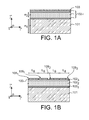
- the starting material or component of the process can be a substrate formed of a first layer 101 of semiconductor material, for example based on Si.
- the first layer 101 is intended to serve as a mechanical support and has a thickness e 1 , preferably very large relative to the thickness of all other layers of the device.
- the layer 101 may have a thickness for example of the order of ten micrometers or several tens of micrometers.
- This "prestressed” layer may have an intrinsic stress that can be biaxial in a plane perpendicular to the surface of the first layer 101.
- the prestressed layer may be formed for example by CVD (CVD for "Chemical Vapor Deposition") or LPCVD (LPCVD for "Low Pressure Chemical Vapor Deposition”).
- the prestressed layer may for example be based on a semiconductor material such as SiGe.
- the prestressed layer may be based on a dielectric material such as Si x N y or Al 2 O 3 .
- the stress can be adjusted according to the proportion of Si.
- the stress exerted by the preload layer can be at least 100 MPa, for example from order of 1 GPa.
- An insulating layer 102 may be formed on the first support layer 101 based on semiconductor material.
- the insulating layer 102 may be formed of several layers, including said preload layer.
- the insulating layer 102 may be formed of a first layer 102 1 based on dielectric material, for example SiO 2 , resting on the first layer 101 of semiconductor material.
- the first layer 102 1 based on dielectric material may have a thickness for example of the order of several nanometers, for example of the order of 10 nanometers.
- the first layer 102 1 may be provided based on a dielectric material to promote the adhesion of a stack of layers on the first layer 101 of semiconductor material.
- the first layer 102 1 based on dielectric material such as SiO 2 can thus serve as a bonding layer or mechanical strength, and can be used to bond the layer prestress 102 2 , for example based on Si 3 N 4 , to the layer 101 of semiconductor support.
- the insulating layer 102 may also be formed of a second layer 102 2 based on dielectric material, for example Si 3 N 4 , resting on the first layer 101 of semiconductor material.
- the second layer 102 2 based on dielectric material may be said preload layer.
- the stress in the second layer 102 2 of dielectric material is an intrinsic stress that can be bi-axial in a plane perpendicular to the main plane of the substrate (the main plane of the substrate being defined throughout the description and on the Figure 1A by a plane parallel to the plane [O; i ; k ] an orthogonal reference [O; i ; j ; k ]).
- the layer of dielectric material 102 2 prestressing is subjected to a constraint of a given type, for example a tensile stress.
- the stress to which the layer of dielectric material 102 2 is subjected may for example be of the order of 1.5 GPa.
- the insulating layer 102 may also comprise a third layer 102 3 based on dielectric material, for example SiO 2 , resting on the first layer 101 of semiconductor material.
- the third layer 102 3 may be chosen for its electrical insulation properties and have a thickness for example of the order of ten nanometers, for example of the order of 16 nanometers.
- the thickness e 2 of the second layer of dielectric material 102 2 prestressing is preferably provided greater than the thickness of the first and third layers 102 1 and 102 3 of dielectric material.
- the second layer of dielectric material 102 2 may have a thickness e 2 at least 10 times greater than that of the first and third layers 102 1 and 102 3 of dielectric material.
- the prestressed layer 102 2 may have a thickness for example between 50 nanometers and 200 nanometers, for example of the order of 120 nanometers.
- the prestressed layer 102 2 may have a thickness provided 5 to 10 times the thickness of said thin semi-conducting layer 103.
- a SOIM type substrate (SOIM for "Silicon on Insulating Multiple Layer”) comprising a plurality of dielectric layers between a semiconductor carrier layer and a semiconductor layer in which active zones are intended to be produced, can thus be formed ( Figure 1A ).
- the thickness of the support layer 101 is provided so as to provide sufficient mechanical rigidity to limit the relaxation of the prestressing layer 102 2 by a route other than etching.
- the thickness e 2 of the prestressing layer 102 2 is preferably small compared with the thickness e 1 of the layer 101 of the substrate, for example at least 20 times less than the thickness of the layer 101 of the substrate.
- the semiconductor layer 103 is etched in order to produce several semiconductor islands or semiconductor zones 108 1 , 108 2 , 109 1 , 109 2 , separated from the semiconductor layer 103.
- Semiconductor zones 108 1 , 108 2 , 109 1 , 109 2 are intended to form active zones of transistors.
- the semiconductor zones 108 1 , 108 2 , 109 1 , 109 2 produced, are a first zone 108 1 , and a second zone 108 2 , formed with a first critical dimension L 8 , and a third zone 109 1 , and a fourth zone 109 2 , formed with a second critical dimension L 9 , different from the first critical dimension L 8 .
- the first critical dimension L 8 is chosen to be smaller than a predetermined distance called "limit length" Lc.
- the first critical dimension L 8 is for example between one or more tens of nanometers and ten times the thickness of the semiconductor layer 103.
- the first critical dimension L 8 may for example be between 40 and 200 nanometers and for example of the order of 70 nanometers.
- the second critical dimension L 9 is chosen for its greater than the predetermined limit length Lc.
- the second critical dimension L 9 may for example be between about ten times the thickness of the semiconductor layer 103 and several tens of times the thickness e 2 of the layer 102 2 prestressing.
- the second critical dimension L 9 may be for example between 50 and 300 nanometers and for example of the order of 100 nanometers
- critical dimension will be called the smallest dimension made in a thin layer or in a stack of thin layers, except for the thickness of this thin layer or of this stack of thin layers.
- the third zone 109 1 and the fourth zone 109 2 semiconductors are spaced apart from each other by a distance that may be for example between several nanometers and several hundred nanometers.
- the etching of the layer 103 can be performed by selective etching, for example silicon with respect to SiO 2 .
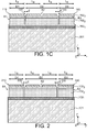
- the preload layer 102 2 is etched perpendicularly to its surface.
- Trenches 110, 120, 130, 140 are formed in particular in the insulating layer 102.
- the trenches 110, 120, 130, 140 are vertical trenches, orthogonal to the main plane of the substrate and that of the prestressed layer 102 2 .
- trenches 110, 120, 130, 140 By forming these trenches 110, 120, 130, 140 blocks B 1 , B 2 , B 3 are defined.
- the trenches 110, 120, 130, 140 pass through the first layer of dielectric material 102 1 , as well as at least a portion of the thickness of the prestress layer 102 2 , possibly over the entire thickness of this prestressed layer 102 2 .
- the trenches 110, 120, 130, 140 may be produced using one or more anisotropic etching steps.
- trenches 110, 120, 130, 140 are formed on either side of each of the semiconductor regions 108 1 and 108 2 of critical dimension L 8 .
- the trenches 110, 120, 130, 140 are in particular formed in the extension of the sidewalls of the semiconductor zones 108 1 and 108 2 having the first critical dimension L 8 .
- the formation of the trenches relaxes 110, 120, 130, 140, the prestressed layer 102 2 at its upper surface.
- a first trench 110 is formed in the extension of a first side of the first semiconductor zone 108 1
- a second trench 120 is in turn made in the extension of a second side of the first zone 108 1 semi-conductor conductive, opposite to the first flank.
- a first block B 1 covered with the first zone 108 1 semiconductor is thus formed in the layers of dielectric material 102 2 , 102 3 .
- the critical dimension L 8 of the semiconductor zones 108 1 , 108 2 is provided at least less than the depth of the trenches 110, 120, 130, 140.
- a third trench 130 is made in the extension of a first flank of the fourth zone 108 2 semiconductor, a fourth trench 140 being formed in the extension of a second side of the second zone 108 2 semiconductor.
- a second block B 2 covered with semiconductor zones 109 1 , 109 2 and a third block B 3 covered with the semiconductor zone 108 2 are thus formed in the layers of dielectric material 102 2 , 102 3 .
- the first block B 1 and the third block B 3 have critical dimensions D 1 and D 3 equal to or substantially equal to the critical dimension L 8 of the semiconductor zones 108 1 and 108 2 , and less than the depth of the trenches.
- the second block B 2 can in turn be provided with a critical dimension greater than the depth of the trenches, for example a critical dimension D2 of the order of 300 nanometers.
- a dimension D2 of the order of twice the thickness of the preload layer makes it possible to obtain a good level of compression in the semiconductor zones 109 1 , 109 2 .
- the dimension D2 may be provided at least greater than the depth of the trenches 110, 120, 130, 140.
- a transfer on the semiconductor zones 108 1 , 108 2 , of the stress of the layer 102 2 is achieved.
- An etching performed throughout the thickness of the prestress layer 102 2 allows a greater transfer of the state of stress on the zones 108 1 and 108 2 .
- the critical dimension L 8 (L 8 chosen less than a predetermined length Lc) of the semiconductor zones 108 1 and 108 2 , and of the arrangement of the trenches 110, 120, 130, 140 with respect to these semiconductor zones 108 1 and 108 2 , the type of stress exerted on these semiconductor zones 108 1 and 108 2 is identical to that of the prestressing layer 102 2 .
- the deformation of the semiconductor zones 108 1 and 108 2 is of the same sign as that of the prestressed layer 102 2 .
- the stress of the prestressing layer 102 2 is a stress in tension
- a stress in tension is also exerted on the semiconductor zones 108 1 and 108 2 .
- a stress exerted on a semiconductor zone 108 1 or 108 2 it means a resultant average stress of the set of stresses exerted on this semiconductor zone 108 1 or 108 2 .
- Such a transfer of stress on the semiconductor zones 108 1 and 108 2 is due to edge effects, which occur when the semiconductor zones are formed with a sufficiently small critical dimension chosen less than a predetermined length Lc .
- This limiting length Lc is determined as a function, in particular, of the thickness of the semiconductor layer 103 and of the underlying layers in which the trenches are made, in particular the thickness of the insulating layer 102 3 and the prestress layer 102 2 .
- the type of stress exerted on the semiconductor zones 109 1 and 109 2 is different from that of the prestressed layer 102 2 .
- the deformation of the semiconductor zones 108 1 and 108 2 is of opposite sign to that of the prestressing layer 102 2 .
- the stress of the preload layer 102 2 is a stress in tension
- a compressive stress is exerted on the semiconductor zones 109 1 and 109 2 .
- the trenches 110, 120, 130, 140 make it possible to relax the strain of the second layer of dielectric material 102 2 at the blocks B 1 - B 3, and to transfer the tensile stress at the top of the blocks B 1 and B 3 , that is to say at the level of the semiconductor zones 108 1 , 108 2 .
- the semiconductor zones 108 1 and 108 2 undergo a voltage stress, while the semiconductor zones 109 1 and 109 2 undergo a constraint in compression.
- the first semiconductor zone 108 1 can be voltage-stressed and stressed, for example of the order of a hundred MPa.
- the semiconductor zone 109 1 can be constrained in compression and undergo a stress for example of the order of several hundred MPa.
- a space of at least a predetermined value d can be optionally provided between the mouth of the trenches 120, 130, and the semiconductor zones 109 1 , 109 2 , in order to avoid the edge effects mentioned above on the semiconductor zones 109 1 , 109 2 .
- the semiconductor zones 109 1 and 109 2 having a critical dimension L 9 chosen greater than Lc, this space d can be optional and can be low or zero.
- the depth of the trenches 110, 120, 130, 140 can be predicted and modulated according to the level of stress that it is desired to impart to the semiconductor zones 108 1 , 108 2 , 109 1 , 109 2 .
- the trenches 110, 120, 130, 140 may then be filled, for example using an insulating material 145.
- the insulating material 145 for filling the trenches may itself have a state of stress.
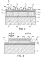
- a gate dielectric zone 160 and a gate 162 on the dielectric zone 160 can be formed.
- Spacers 163, 164 on the sides of the grid 160 can then be made.
- one or more scattering and / or implantation doping steps can be performed to complete the formation of source areas 171 and drain 172.
- a device comprising transistors T 1 and T 4 provided with channel regions respectively formed in semiconductor zones 108 1 , 108 2 voltage stresses, has thus been realized and transistors T 2 and T 3 , comprising channel zones. respectively in compression-resistant semiconductor zones 109 1 , 109 2 have thus been realized ( figure 3 ).
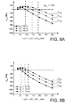
- the state of stress of each of the semiconductor zones 108 1 , 108 2 , 109 1 , 109 2 can be estimated by means of numerical calculations carried out with a simulation tool for example, such as the ANSYS-v10 tool from ANSYS.
- FIG. 6A shows, through the stress field C1, that in a given thickness of their upper face, for example of the order of 3 to 4 nanometers, the semiconductor zones 108 1 , 108 2 have a positive average overall stress and are thus voltage-strained.
- the stress fields C 2 and C 3 show that in a given thickness of their upper face, for example of the order of 3 to 4 nanometers, the semiconductor zones 109 1 , 109 2 have a negative average overall stress and are thus constrained in compression.
- vertical trenches 210, 220, 230, 240, orthogonal to the main plane of the substrate of the prestressing layer 102 2 , passing through the third layer of dielectric material 102 3 and the entire thickness of the layer are carried out.
- the semiconductor layer 103 resting on the insulating layer 102 may also be a prestressed layer, that is to say having an intrinsic stress.
- the semiconductor layer 103 may for example have a biaxial stress in a plane perpendicular to the main plane of the substrate.
- the pre-deformation of the semiconductor layer 103 can in this case be obtained for example by heteroepitaxy or by molecular bonding.
- the semiconductor zone 508 rests on an insulating zone 502, for example based on SiO 2 , itself lying on a prestressing zone 502 2 , for example based on Si 3 N 4 , itself resting on an insulating layer 502. 1 , for example based on SiO 2 .
- This semiconductor zone 508 is intended to contain the channel of a transistor and corresponds to the region in which a charge transport is carried out.
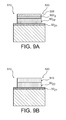
- Trenches 510, 520 are formed on either side of the zones 508, 502 3 , 502 2 , up to the insulating layer 502 1 ( Figure 9A ).
- Simulations were performed with the ANSYS tool for several dimensions L ZA of the semiconductor region 508, and for different thicknesses e if this semiconductor region 508, and various thicknesses and an SiO2 insulating layer 502 3 based on SiO 2 .
- the thickness of the layer 502 2 preload has been fixed. This thickness is expected to be large in front of the thicknesses of the semiconducting zone 508 and the zone 502 1 , for a nitride-based preload layer 502 2 having a thickness set at 200 nm.
- the limit length Lc corresponds to the limit value for which the average stress ⁇ moy of the semiconductor zone 508 changes sign and goes from the voltage to the compression.
- Lc () The limit values obtained for different thicknesses denoted Lc () are represented by means of discontinuous vertical lines on the Figures 8A to 8D .
- a first method is thus to predict the thickness and the composition of the layers 50 3 , 502 2 , 502 3 and use such simulations to determine Lc. For a given thickness of the layer 502 2 , this critical length Lc increases with the thickness of the semiconducting zone 508. Similarly, for a given thickness of this zone 508, the limit length Lc increases with the thickness of the layer insulating 502 3 .
- an empirical relationship is used between the established limit length Lc, and the different dimensions of the structure such that the thickness of the prestressed layer 502 2, 502 of the insulating layer 3, with a an analytical model such as that of document [1]: Hu et al., Appl. Phys., 50 (7), p. 4661, July 1979, and [2]: Hu et al., Appl. Phys., 70 (6), p. R53, September 1991 can be used.
- This relation can be established by possibly using an approximation according to which one considers a semiconductor zone 508 of small thickness in front of that of the substrate, whose stress ⁇ 0 is uniform in the main plane of this zone and zero in the direction of its thickness.
- a relation between the ratio of the average stress ⁇ moy and the stress ⁇ 0 : ( ⁇ moy / ⁇ 0 ), and between the reduced parameter (KL / h) can be used.
- the bending stiffness of these two layers ((e Si ⁇ SiO 2 ) and (e Si )) is preferably constant.
- I i represents the moment of inertia of the layer i.
- the results represented by this curve C 100 relate to two exemplary embodiments: a first in which the thickness e SiO 2 is of the order of 16 nm with a thickness e Si of the order of 15 nanometers and a second embodiment in which a thickness of oxide e SiO2 of the order of 16 nm with a thickness of silicon e Si of the order of 20 nm.
- This curve C 100 is canceled for a value of: / e eq K ⁇ The ZA vs ⁇ 8.77
- Limit length values L c can be extracted for different pairs (e SiO 2 , e Si ) by extrapolating the curves as illustrated on the Figures 8A-8B then can compare these values with those calculated using the empirical formula given above.
- the figure 4 illustrates a variant of the microelectronic device example described above in connection with the figure 2 .
- the device comprises semiconductor zones 308 1 , 308 2 , 309 1 , 309 2 , intended to form active zones distributed on the same insulating block B 10 .
- a first semiconductor zone 308 1 , and a second semiconductor zone 308 2 have a critical dimension L 8 provided lower than the predetermined length Lc / 2, whose determination methods have been given above, and which is determined in particular as a function of the thickness of the semiconductor zones of the layers 102 3 and 102 2 .
- a third semiconductor region 309 1 , and a fourth semiconductor zone 309 2 have a critical dimension which may also be less than or equal to the predetermined length Lc.
- the semiconductor zones 308 1 , 309 1 , 308 2 , 309 2 are constrained and rest on an etched block B 10 formed in a stack of thin layers comprising a prestressed layer 102 2 .
- Trenches 310, 320 are formed in a portion of the thickness of the prestressed layer 102 2, on either side of the etched block B 10.
- the trenches 310, 320 have a depth greater than the critical dimension L 8 of the semiconductor zones 308 1 and 308 2 .
- a trench 320 is formed in the extension of a flank of the semiconductor zone 308 2 .
- Another trench 310 is made in the extension of a flank of the semiconductor zone 308 1 .
- a transfer of the stress of the prestressing layer 102 2 to the top of the block B 10 is implemented in the semiconductor zones 308 1 and 308 2 .
- the semiconductor zones 308 1 and 308 2 are also voltage-strained.
- a semiconductor zone 309 2 juxtaposed with the semiconductor zone 308 2 , for its part, is located at a distance d of at least Lc / 2 from the trench 320.
- the semiconductor zones 109 1 and 109 2 are constrained in compression or have a mean stress corresponding to a compressive stress.
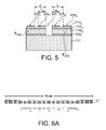
- the device comprises semiconductor zones 408 1 , 408 2 constrained according to a first type of stress, for example a stress in tension, and semiconductor zones 409 1 , 409 2 constrained according to a second type of stress, for example a compressive stress.
- a first type of stress for example a stress in tension
- semiconductor zones 409 1 , 409 2 constrained according to a second type of stress, for example a compressive stress.
- the semiconductor zones 408 1 , 409 1 may have been formed from a pre-stressed semiconductor layer, and rest on a first block B 100 formed of a stack of layers of dielectric material 102 1 , 102 2, 102 3, at least one layer 102 2 preload, for example voltage.
- the semiconductor zones 408 2 , 409 2 may have been formed from said layer pre-stressed semiconductor, and rest on a second block B 200 formed in the stack of layers of dielectric material 102 1 , 102 2 , 102 3 .
- the semiconductor zones 408 1 , 408 2 are provided with a critical dimension L 8 ⁇ Lc / 2, with Lc the limiting length of which determination methods have been given above, and which is a function of the thickness of the semi zones. as well as the respective thickness of the layers 102 2 and 102 3 .
- a trench 410 separates the first block B 100 from the second block B 200 .
- This trench is made in the extension of a flank of the semiconductor zone 408 1 and a flank of the semiconductor zone 408 2 .
- the semiconducting zones 409 1 and 409 2 are located at a distance d of at least Lc / 2 from the trench 410, in order to make it possible to give these semiconducting zones 409 1 and 409 2 a constraint. of sign opposite to that of the stress of the preload layer and the stress of the semiconductor zones 408 1 , 408 2 .
Abstract
Description
La présente invention se rapporte au domaine des circuits intégrés, et plus particulièrement à celui des transistors, et a pour but de présenter un procédé de réalisation d'un dispositif microélectronique doté de plusieurs transistors aux performances électriques améliorées, et en particulier dans lequel, sur un même substrat, un ou plusieurs transistors sont contraints en tension tandis qu'un ou plusieurs autres transistors sont contraints en compression.The present invention relates to the field of integrated circuits, and more particularly to that of transistors, and aims to present a method for producing a microelectronic device having a plurality of transistors with improved electrical performance, and in particular in which, on the same substrate, one or more transistors are voltage-stressed while one or more other transistors are constrained in compression.
Dans le transistor MOS (MOS pour Metal Oxide Semiconductor), deux réservoirs de porteurs de charges : la source et le drain, sont séparés par une barrière de potentiel formée par le canal. Cette barrière est contrôlée par une grille d'une longueur qui peut varier de plusieurs nanomètres à plusieurs dizaines de nanomètres. La grille est séparée du canal par un diélectrique de grille.In the MOS transistor (MOS for Metal Oxide Semiconductor), two charge carrier reservoirs: the source and the drain, are separated by a potential barrier formed by the channel. This barrier is controlled by a grid of a length that can vary from several nanometers to several tens of nanometers. The gate is separated from the channel by a gate dielectric.
On cherche constamment à diminuer la dimension des transistors. Dans les procédés existants de réalisation de dispositifs microélectroniques, la mise en oeuvre d'une couche de silicium contraint sur un substrat SOI (SOI pour « Silicon on Insulator » ou silicium sur isolant), a permis d'augmenter à la fois la mobilité des porteurs grâce à l'effet d'une contrainte mécanique sur un matériau semi-conducteur et la densité d'intégration grâce à une isolation électrique du transistor. L'introduction de contraintes mécaniques dans le canal de conduction permet d'améliorer très fortement la mobilité des porteurs, et donc les performances électriques des transistors.We are constantly trying to reduce the size of the transistors. In existing methods for producing microelectronic devices, the implementation of a silicon layer forced on a SOI substrate (SOI for "Silicon on Insulator" or "Silicon on Insulator"), has made it possible to increase both the mobility of the carriers thanks to the effect of a mechanical stress on a semiconductor material and the integration density thanks to an electrical isolation of the transistor. The introduction of mechanical stresses in the conduction channel makes it possible to very greatly improve the mobility of the carriers, and therefore the electrical performance of the transistors.
Une contrainte mécanique bi-axiale en tension peut permettre d'augmenter de manière importante la mobilité des électrons pour les transistors NMOS.A biaxial mechanical stress stress can significantly increase the mobility of electrons for NMOS transistors.
Pour les transistors PMOS, une contrainte en compression permet quant à elle d'obtenir un gain en mobilité des trous.For PMOS transistors, a compressive stress makes it possible to obtain a gain in mobility of the holes.
Actuellement, il existe différentes méthodes pour permettre de contraindre un canal de transistor. On peut utiliser un substrat standard avec un canal contraint en cours de fabrication du transistor. On peut également utiliser un substrat modifié précontraint sur lequel on réalise une zone de canal.Currently, there are different methods to allow to constrain a transistor channel. It is possible to use a standard substrate with a constrained channel during the fabrication of the transistor. It is also possible to use a prestressed modified substrate on which a channel zone is made.
Afin d'améliorer la mobilité des porteurs de charge à la fois dans les transistors NMOS et PMOS, des procédés permettant de former, sur un même substrat, une ou plusieurs zones semi-conductrices contraintes en tension et une ou plusieurs zones semi-conductrices contraintes en compression sont apparus.In order to improve the mobility of the charge carriers in both the NMOS and PMOS transistors, methods for forming, on the same substrate, one or more voltage-constrained semiconductor zones and one or more constrained semiconductor zones. in compression appeared.
Le document
A coté de ce premier empilement, un deuxième empilement est réalisé. Ce deuxième empilement est formé d'une deuxième couche de matériau diélectrique contrainte en tension formée sur le substrat et d'une deuxième couche de matériau semi-conducteur placée sur la couche de matériau diélectrique contrainte en tension. La deuxième couche diélectrique transfère des contraintes en compression à la deuxième couche de matériau semi-conducteur. Un tel procédé nécessite la réalisation d'une zone diélectrique enterrée contrainte en tension et d'une zone diélectrique enterrée contrainte en compression.Next to this first stack, a second stack is made. This second stack is formed of a second layer of voltage-constrained dielectric material formed on the substrate and a second layer of semiconductor material placed on the layer of dielectric material stressed in tension. The second dielectric layer transfers compressive stresses to the second layer of semiconductor material. Such a method requires the realization of a buried dielectric zone voltage-stressed and a buried dielectric zone constrained in compression.
Le document
Le document
Un tel procédé est complexe et long à mettre en oeuvre dans la mesure où il nécessite plusieurs étapes d'épitaxies successives différentes.Such a process is complex and time-consuming in that it requires several different successive epitaxial steps.
Il se pose le problème de trouver un nouveau procédé de réalisation d'un dispositif microélectronique comprenant une ou plusieurs zones semi-conductrices contraintes en tension et d'une ou plusieurs zones semi-conductrices contraintes en compression, qui ne comporte pas les inconvénients mentionnés ci-dessus.There is the problem of finding a new method for producing a microelectronic device comprising one or more voltage-constrained semiconductor zones and one or more compression-constrained semiconductor zones, which does not have the drawbacks mentioned above. -above.
L'invention concerne en particulier un procédé de réalisation d'un dispositif microélectronique comprenant une ou plusieurs zones semi-conductrices contraintes en tension et une ou plusieurs zones semi-conductrices contraintes en compression, qui ne comporte pas les inconvénients mentionnés ci-dessus, dans lequel on forme des tranchées dans une couche précontrainte au-dessus de laquelle des zones semi-conductrices ont été préalablement réalisées, les dimensions et l'agencement des tranchées par rapport aux zones semi-conductrices, ainsi que la dimension critique des zones semi-conductrices étant prévues de manière à former au moins une zone semi-conductrice contrainte en compression et au moins une zone semi-conductrice contrainte en tension.The invention relates in particular to a method for producing a microelectronic device comprising one or more voltage-constrained semiconductor zones and one or more compression-constrained semiconductor zones, which does not have the disadvantages. mentioned above, in which trenches are formed in a prestressed layer above which semiconductor zones have previously been formed, the dimensions and the arrangement of the trenches with respect to the semiconductor zones, as well as the dimension critical of the semiconductor zones being provided so as to form at least one compression-constrained semiconductor zone and at least one voltage-constrained semiconductor zone.
Selon un premier aspect, l'invention concerne un procédé de réalisation d'un dispositif microélectronique comportant, sur un même support : au moins une zone semi-conductrice contrainte en tension, et au moins une zone semi-conductrice contrainte en compression.According to a first aspect, the invention relates to a method for producing a microelectronic device comprising, on a same support: at least one voltage-constrained semiconductor zone, and at least one semiconductor zone constrained in compression.
Ce procédé comprend des étapes consistant à :
- a) réaliser à partir d'un empilement de couches reposant sur un substrat et comportant au moins une couche semi-conductrice située au-dessus d'au moins une couche précontrainte, d'au moins une première zone semi-conductrice ayant une première dimension critique L8 choisie inférieure à une longueur prédéterminée Lc, et d'au moins une deuxième zone semi-conductrice ayant une deuxième dimension critique L9 choisie supérieure à ladite longueur prédéterminée Lc,
- b) réaliser une ou plusieurs tranchées dans au moins une partie de l'épaisseur de ladite couche précontrainte, au moins une première tranchée parmi lesdites tranchées étant située dans le prolongement d'au moins un premier flanc de ladite première zone semi-conductrice, la longueur limite Lc ayant été déterminée au moins en fonction de l'épaisseur des couches de l'empilement dans lesquelles les tranchées sont réalisées.
- a) producing from a stack of layers resting on a substrate and comprising at least one semiconductor layer situated above at least one prestress layer, at least one first semiconductor zone having a first dimension critical L 8 chosen less than a predetermined length Lc, and at least one second semiconductor zone having a second critical dimension L 9 chosen greater than said predetermined length Lc,
- b) forming one or more trenches in at least a portion of the thickness of said prestressing layer, at least a first trench among said trenches being located in the extension of at least a first side of said first zone; semiconductor, the limit length Lc having been determined at least as a function of the thickness of the layers of the stack in which the trenches are made.
La première zone semi-conductrice a, suite à l'étape b) une contrainte du même type que ladite couche précontrainte, par exemple une contrainte en tension, tandis que ladite deuxième zone semi-conductrice a une contrainte d'un type opposé à celui que ladite couche précontrainte, par exemple une contrainte en compression.The first semiconductor zone has, following step b) a stress of the same type as said prestressed layer, for example a voltage stress, while said second semiconductor zone has a constraint of a type opposite to that that said preload layer, for example a compressive stress.
Selon un autre aspect, l'invention concerne un procédé de réalisation d'un dispositif microélectronique comportant sur un même support : au moins une zone semi-conductrice contrainte en tension, et au moins une zone semi-conductrice contrainte en compression, le procédé comportant les étapes consistant à :
- a) réaliser à partir d'un empilement de couches reposant sur un substrat et comportant au moins une couche semi-conductrice située au-dessus d'au moins une couche précontrainte, d'au moins une première zone semi-conductrice ayant une première dimension critique L8 prévue inférieure à une longueur prédéterminée Lc,
- b) réalisation d'une ou plusieurs tranchées dans au moins une partie de l'épaisseur de ladite couche précontrainte, au moins une première tranchée parmi lesdites tranchées étant située dans le prolongement d'au moins un premier flanc de ladite première zone semi-conductrice, un espace d, tel que d > Lc/2 est prévu entre ladite deuxième zone semi-conductrice et lesdites tranchées, la longueur limite Lc ayant été déterminée en fonction de l'épaisseur des couches de l'empilement dans lesquelles les tranchées ont été réalisées.
- a) producing from a stack of layers resting on a substrate and comprising at least one semiconductor layer situated above at least one prestress layer, at least one first semiconductor zone having a first dimension critical L 8 predicted lower than a predetermined length Lc,
- b) forming one or more trenches in at least a portion of the thickness of said prestressing layer, at least a first trench among said trenches being located in the extension of at least a first sidewall of said first semiconductor zone; a space d such that d> Lc / 2 is provided between said second semiconductor zone and said trenches, the limiting length Lc having been determined as a function of the thickness of the layers of the stack in which the trenches were made.
La première zone semi-conductrice a, suite à l'étape b), une contrainte du même type que ladite couche précontrainte, ladite deuxième zone semi-conductrice ayant une contrainte d'un type opposé à celui que ladite couche précontrainte.The first semiconductor zone has, following step b), a stress of the same type as said preload layer, said second semiconductor zone having a constraint of a type opposite to that said preload layer.
Selon cet autre aspect, la deuxième zone semi-conductrice peut éventuellement avoir une dimension critique inférieure ou égale à la longueur limite Lc. De par l'espace d prévu entre les tranchées et la deuxième zone semi-conductrice, le type de contrainte auquel la deuxième zone semi-conductrice est soumise est différent de celui auquel la première zone semi-conductrice est soumise.In this other aspect, the second semiconductor zone may optionally have a critical dimension less than or equal to the limit length Lc. Due to the gap between the trenches and the second semiconductor zone, the type of stress to which the second semiconductor zone is subjected is different from that to which the first semiconductor zone is subjected.
La profondeur des tranchées peut être prévue de l'ordre de la demi-longueur de la zone semi-conductrice.The depth of the trenches can be provided on the order of half the length of the semiconductor zone.
La profondeur des tranchées peut être prévue inférieure à la dimension critique de ladite deuxième zone semi-conductrice.The depth of the trenches may be less than the critical dimension of said second semiconductor zone.
Parmi lesdites tranchées au moins une autre tranchée peut être réalisée dans le prolongement d'un deuxième flanc de ladite première zone semi-conductrice, opposé audit premier flanc.Among said trenches at least one other trench can be made in the extension of a second side of said first semiconductor zone, opposite said first sidewall.
Selon une possibilité, la deuxième zone semi-conductrice et la première zone semi-conductrice peuvent reposer sur un même bloc gravé à l'étape b) dans ledit empilement, avec au moins deux desdites tranchées situées de part et d'autre dudit même bloc gravé.According to one possibility, the second semiconductor zone and the first semiconductor zone may rest on the same block etched in step b) in said stack, with at least two of said trenches located on both sides of the same engraved block.
Selon une possibilité, lesdites tranchées peuvent être réalisées dans une partie de l'épaisseur de la couche précontrainte.According to one possibility, said trenches can be made in part of the thickness of the prestressing layer.
Selon une variante, lesdites tranchées peuvent être réalisées dans toute l'épaisseur de la couche précontrainte.According to a variant, said trenches can be made throughout the thickness of the prestressing layer.
La profondeur des tranchées peut être prévue en fonction du niveau de contrainte que l'on souhaite appliquer à la première zone semi-conductrice et à la deuxième zone semi-conductrice.The depth of the trenches can be provided according to the level of stress that it is desired to apply to the first semiconductor zone and the second semiconductor zone.
Ladite couche précontrainte peut être une contrainte bi-axiale dans un plan orthogonal au plan principal du substrat.Said prestressed layer may be a bi-axial constraint in a plane orthogonal to the main plane of the substrate.
Selon une possibilité, ladite couche précontrainte peut être à base d'un matériau diélectrique tel que du Si3N4.According to one possibility, said preload layer may be based on a dielectric material such as Si 3 N 4 .
Ledit empilement peut comprendre une couche d'adhérence entre la couche précontrainte et la couche semi-conductrice.Said stack may comprise an adhesion layer between the preload layer and the semiconductor layer.
Selon une mise en oeuvre particulière, ladite couche semi-conductrice peut être précontrainte ou avoir une contrainte intrinsèque.According to one particular embodiment, said semiconductor layer may be prestressed or have intrinsic stress.
Ladite couche précontrainte peut être située sur une couche de matériau diélectrique reposant sur une couche de support semi-conductrice.Said prestressed layer may be located on a layer of dielectric material resting on a semiconductor support layer.
Le procédé peut comprendre en outre : le remplissage des tranchées à l'aide d'un matériau isolant.The method may further include: filling the trenches with an insulating material.
Le procédé peut comprendre également : la formation sur une ou plusieurs ou sur l'ensemble desdites zones semi-conductrices d'au moins une zone de diélectrique de grille et d'au moins une grille sur la zone de diélectrique de grille.The method may also include: forming on one or more or all of said semiconductor regions at least one gate dielectric area and at least one gate on the gate dielectric area.
Ainsi, des transistors MOS peuvent être formés sur la première zone semi-conductrice et sur la deuxième zone semi-conductrice.Thus, MOS transistors may be formed on the first semiconductor region and the second semiconductor region.
Ladite couche de matériau diélectrique peut être une couche précontrainte en tension, suite à l'étape b), ladite première zone semi-conductrice étant une couche contrainte en tension, ladite deuxième zone semi-conductrice étant contrainte en compression.Said layer of dielectric material may be a voltage preload layer, following step b), said first semiconductor zone being a voltage-stressed layer, said second semiconductor zone being constrained in compression.
La présente invention sera mieux comprise à la lecture de la description d'exemples de réalisation donnés, à titre purement indicatif et nullement limitatif, en faisant référence aux dessins annexés sur lesquels :
- les
figures 1A-1C , illustrent un exemple de procédé selon l'invention, de réalisation d'un dispositif microélectronique doté de zones semi-conductrices subissant des contraintes différentes sur un même substrat, - la
figure 2 illustre une variante de procédé de réalisation d'un procédé suivant l'invention, - les
figures 3 à 5 illustrent, des exemples de dispositifs microélectroniques obtenus à l'aide d'un procédé selon l'invention, - les
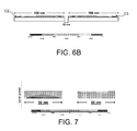
figures 6A à 6B , et7 montrent, des résultats de simulations sous forme de champs de contrainte exercées sur les zones semi-conductrices de dispositifs suivant l'invention, - les
figures 8A-8D donnent des exemples de courbes d'évolution de la contrainte moyenne exercée sur une zone semi-conductrice obtenue à l'aide d'un procédé suivant l'invention, en fonction de sa dimension critique, pour différentes valeurs d'épaisseur de cette zone et d'un empilement de couches sous-jacentes à cette zone et comportant au moins une couche précontrainte, - les
figures 9A-9B donnent respectivement un exemple de structure et un exemple de structure équivalente, utilisés pour la détermination d'une longueur limite Lc, par rapport à laquelle la dimension critique des zones semi-conductrices d'un dispositif microélectronique mis en oeuvre suivant l'invention est prévue, - la
figure 10 illustre une inversion du type de contrainte, de la tension vers la compression, exercée sur une zone semi-conductrice obtenue à l'aide d'un procédé suivant l'invention, en fonction de la dimension critique choisie pour cette zone semi-conductrice.
- the
Figures 1A-1C illustrate an example of a process according to the invention for producing a microelectronic device provided with semiconductor zones undergoing different stresses on the same substrate, - the
figure 2 illustrates an alternative method of producing a method according to the invention, - the
Figures 3 to 5 illustrate, examples of microelectronic devices obtained using a method according to the invention, - the
Figures 6A to 6B , and7 show results of simulations in the form of stress fields exerted on the semiconductor zones of devices according to the invention, - the
Figures 8A-8D give examples of curves of evolution of the average stress exerted on a semiconductor zone obtained by means of a process according to the invention, as a function of its critical dimension, for different values of thickness of this zone and a stack of layers underlying this zone and comprising at least one prestressing layer, - the
Figures 9A-9B give respectively an exemplary structure and an example of equivalent structure, used for the determination of a limit length Lc, with respect to which the critical dimension of the semiconductor zones of a microelectronic device implemented according to the invention is provided. , - the
figure 10 illustrates an inversion of the type of stress, of the tension towards the compression, exerted on a semiconductor zone obtained by means of a method according to the invention, as a function of the critical dimension chosen for this semiconductor zone.
Des parties identiques, similaires ou équivalentes des différentes figures portent les mêmes références numériques de façon à faciliter le passage d'une figure à l'autre.Identical, similar or equivalent parts of the different figures bear the same numerical references so as to facilitate the passage from one figure to another.
Les différentes parties représentées sur les figures ne le sont pas nécessairement selon une échelle uniforme, pour rendre les figures plus lisibles.The different parts shown in the figures are not necessarily uniform scale, to make the figures more readable.
Un exemple de procédé suivant l'invention, de réalisation d'un dispositif microélectronique comprenant au moins une zone semi-conductrice contrainte en tension et au moins une autre zone semi-conductrice contrainte en compression, va à présent être donné, en liaison avec les
Le matériau ou composant de départ du procédé (
La première couche 101 est prévue pour servir de support mécanique et a une épaisseur e1, de préférence très grande par rapport à l'épaisseur de l'ensemble des autres couches du dispositif. La couche 101 peut avoir une épaisseur par exemple de l'ordre d'une dizaine de micromètres ou de plusieurs dizaines de micromètres.The
Au dessus de la couche 101 de support, figure au moins une couche dite « précontrainte ». Cette couche « précontrainte » peut avoir une contrainte intrinsèque qui peut être bi-axiale dans un plan perpendiculaire à la surface de la première couche 101.Above the
La couche précontrainte peut être formée par exemple par CVD (CVD pour « Chemical Vapour Deposition ») ou LPCVD (LPCVD pour « Low Pressure Chemical Vapour Deposition »). La couche précontrainte peut être par exemple à base d'un matériau semi-conducteur tel que du SiGe.The prestressed layer may be formed for example by CVD (CVD for "Chemical Vapor Deposition") or LPCVD (LPCVD for "Low Pressure Chemical Vapor Deposition"). The prestressed layer may for example be based on a semiconductor material such as SiGe.
Selon une autre possibilité, la couche précontrainte peut être à base d'un matériau diélectrique tel que du SixNy ou de l'Al2O3.According to another possibility, the prestressed layer may be based on a dielectric material such as Si x N y or Al 2 O 3 .
Dans un cas où la couche précontrainte est à base de SixNy, la contrainte peut être ajustée en fonction de la proportion de Si. La contrainte exercée par la couche précontrainte peut être d'au moins 100 MPa, par exemple de l'ordre de 1 GPa.In a case where the prestressed layer is based on Si x N y , the stress can be adjusted according to the proportion of Si. The stress exerted by the preload layer can be at least 100 MPa, for example from order of 1 GPa.
Une couche isolante 102 peut être formée sur la première couche 101 de support à base de matériau semi-conducteur. La couche isolante 102 peut être formée de plusieurs couches, dont ladite couche précontrainte.An insulating
La couche isolante 102 peut être formée d'une première couche 1021 à base de matériau diélectrique, par exemple du SiO2, reposant sur la première couche 101 de matériau semi-conducteur. La première couche 1021 à base de matériau diélectrique peut avoir une épaisseur par exemple de l'ordre de plusieurs nanomètres, par exemple de l'ordre de 10 nanomètres.The insulating
La première couche 1021 peut être prévue à base d'un matériau diélectrique pour favoriser l'adhésion d'un empilement de couches sur la première couche 101 de matériau semi-conducteur. La première couche 1021 à base de matériau diélectrique tel que du SiO2 peut ainsi servir de couche d'adhérence ou de tenue mécanique, et peut servir à lier la couche précontrainte 1022, par exemple à base de Si3N4, à la couche 101 de support semi-conductrice.The
La couche isolante 102 peut être également formée d'une deuxième couche 1022 à base de matériau diélectrique, par exemple du Si3N4, reposant sur la première couche 101 de matériau semi-conducteur. La deuxième couche 1022 à base de matériau diélectrique, peut être ladite couche précontrainte. La contrainte dans la deuxième couche 1022 de matériau diélectrique est une contrainte intrinsèque qui peut être bi-axiale dans un plan perpendiculaire au plan principal du substrat (le plan principal du substrat étant défini dans toute la description et sur la
La couche isolante 102 peut également comprendre une troisième couche 1023 à base de matériau diélectrique, par exemple du SiO2, reposant sur la première couche 101 de matériau semi-conducteur. La troisième couche 1023 peut être choisie pour ses propriétés d'isolation électrique et avoir une épaisseur par exemple de l'ordre d'une dizaine de nanomètres, par exemple de l'ordre de 16 nanomètres.The insulating
L'épaisseur e2 de la deuxième couche de matériau diélectrique 1022 précontrainte est prévue de préférence supérieure à l'épaisseur des première et troisième couches 1021 et 1023 de matériau diélectrique. La deuxième couche de matériau diélectrique 1022 peut avoir une épaisseur e2 au moins 10 fois supérieure à celle des première et troisième couches 1021 et 1023 de matériau diélectrique. La couche précontrainte 1022 peut avoir une épaisseur comprise par exemple entre 50 nanomètres et 200 nanomètres, par exemple de l'ordre de 120 nanomètres.The thickness e 2 of the second layer of
Sur la couche isolante 102 repose une fine couche semi-conductrice 103, par exemple de l'ordre de 10 nanomètres d'épaisseur dans laquelle plusieurs zones actives sont destinées à être formées. La couche précontrainte 1022 peut avoir une épaisseur prévue 5 à 10 fois l'épaisseur de ladite fine couche semi-conductrice 103.On the insulating
Un substrat de type SOIM (SOIM pour « Silicon on Insulating Multiple layer ») comportant plusieurs couches diélectriques entre une couche semi-conductrice de support et une couche semi-conductrice dans laquelle des zones actives sont destinées à être réalisées, peut être ainsi formé (
L'épaisseur de la couche 101 de support est prévue de manière à assurer une rigidité mécanique suffisante pour limiter la relaxation de la couche précontrainte 1022 par une autre voie que la gravure.The thickness of the
Afin de maintenir un état de contrainte important, l'épaisseur e2 de la couche précontrainte 1022 est de préférence faible devant l'épaisseur e1 de la couche 101 du substrat, par exemple au moins 20 fois inférieure à l'épaisseur de la couche 101 du substrat.In order to maintain a high stress state, the thickness e 2 of the
Ensuite (
La première dimension critique L8, est choisie inférieure à une distance appelée « longueur limite » Lc prédéterminée.The first critical dimension L 8 is chosen to be smaller than a predetermined distance called "limit length" Lc.
La première dimension critique L8 est par exemple comprise entre une ou plusieurs dizaines de nanomètres et une dizaine de fois l'épaisseur de la couche semi-conductrice 103. La première dimension critique L8 peut être par exemple comprise entre 40 et 200 nanomètres et par exemple de l'ordre de 70 nanomètres.The first critical dimension L 8 is for example between one or more tens of nanometers and ten times the thickness of the
Dans cet exemple de réalisation, la deuxième dimension critique L9, est choisie quant à elle supérieure à la longueur limite Lc prédéterminée.In this embodiment, the second critical dimension L 9 is chosen for its greater than the predetermined limit length Lc.
La deuxième dimension critique L9 peut être par exemple comprise entre une dizaine de fois l'épaisseur de la couche semi-conductrice 103 et plusieurs dizaines de fois l'épaisseur e2 de la couche 1022 précontrainte. La deuxième dimension critique L9 peut être par exemple comprise entre 50 et 300 nanomètres et par exemple de l'ordre de 100 nanomètresThe second critical dimension L 9 may for example be between about ten times the thickness of the
Tout au long de la présente description, on appellera « dimension critique » la plus petite dimension réalisée dans une couche mince ou dans un empilement de couches minces, hormis l'épaisseur de cette couche mince ou de cet empilement de couches minces.Throughout the present description, the term "critical dimension" will be called the smallest dimension made in a thin layer or in a stack of thin layers, except for the thickness of this thin layer or of this stack of thin layers.
La troisième zone 1091 et la quatrième zone 1092 semi-conductrices sont espacées entre elles d'une distance qui peut être comprise par exemple entre plusieurs nanomètres et plusieurs centaines de nanomètres.The third zone 109 1 and the fourth zone 109 2 semiconductors are spaced apart from each other by a distance that may be for example between several nanometers and several hundred nanometers.
La gravure de la couche 103 peut être réalisée par gravure sélective, par exemple du silicium par rapport au SiO2.The etching of the
Ensuite (
En formant ces tranchées 110, 120, 130, 140 on définit des blocs B1, B2, B3. Les tranchées 110, 120, 130, 140, traversent la première couche de matériau diélectrique 1021, ainsi qu'au moins une partie de l'épaisseur de la couche précontrainte 1022, éventuellement sur toute l'épaisseur de cette couche précontrainte 1022.By forming these
Les tranchées 110, 120, 130, 140, peuvent être réalisées à l'aide d'une ou plusieurs étapes de gravures anisotropes. Dans cet exemple de réalisation, des tranchées 110, 120, 130, 140, sont formées de part et d'autre de chacune des zones semi-conductrices 1081 et 1082 de dimension critique L8. Les tranchées 110, 120, 130, 140, sont en particulier réalisées dans le prolongement de flancs des zones semi-conductrices 1081 et 1082 ayant la première dimension critique L8.The
La formation des tranchées permet de relaxer 110, 120, 130, 140, la couche précontrainte 1022 au niveau de sa surface supérieure.The formation of the trenches relaxes 110, 120, 130, 140, the
Sur le dispositif de la
La dimension critique L8 des zones semi-conductrices 1081, 1082 est prévue au moins inférieure à la profondeur des tranchées 110, 120, 130, 140. Une troisième tranchée 130 est réalisée dans le prolongement d'un premier flanc de la quatrième zone 1082 semi-conductrice, une quatrième tranchée 140 étant réalisée dans le prolongement d'un deuxième flanc de la deuxième zone 1082 semi-conductrice.The critical dimension L 8 of the semiconductor zones 108 1 , 108 2 is provided at least less than the depth of the
Un deuxième bloc B2 recouvert des zones semi-conductrices 1091, 1092 ainsi qu'un troisième bloc B3 recouvert de la zone semi-conductrice 1082 sont ainsi formés dans les couches de matériau diélectrique 1022, 1023.A second block B 2 covered with semiconductor zones 109 1 , 109 2 and a third block B 3 covered with the semiconductor zone 108 2 are thus formed in the layers of
Le premier bloc B1 et le troisième bloc B3 ont des dimensions critiques D1 et D3 égales ou sensiblement égales à la dimension critique L8 des zones semi-conductrices 1081 et 1082, et inférieures à la profondeur des tranchées.The first block B 1 and the third block B 3 have critical dimensions D 1 and D 3 equal to or substantially equal to the critical dimension L 8 of the semiconductor zones 108 1 and 108 2 , and less than the depth of the trenches.
Le deuxième bloc B2 peut quant à lui être prévu avec une dimension critique supérieure à la profondeur des tranchées, par exemple une dimension critique D2 de l'ordre de 300 nanomètres. Une dimension D2 de l'ordre du double de l'épaisseur de la couche précontrainte permet d'obtenir un bon niveau de compression dans les zones semi-conductrices 1091, 1092.The second block B 2 can in turn be provided with a critical dimension greater than the depth of the trenches, for example a critical dimension D2 of the order of 300 nanometers. A dimension D2 of the order of twice the thickness of the preload layer makes it possible to obtain a good level of compression in the semiconductor zones 109 1 , 109 2 .
La dimension D2 peut quant à elle être prévue au moins supérieure à la profondeur des tranchées 110, 120, 130, 140.The dimension D2 may be provided at least greater than the depth of the
Un transfert sur les zones semi-conductrices 1081, 1082, de la contrainte de la couche 1022 est réalisé. Une gravure effectuée dans toute l'épaisseur de la couche précontrainte 1022 permet un transfert plus important de l'état de contrainte sur les zones 1081 et 1082.A transfer on the semiconductor zones 108 1 , 108 2 , of the stress of the
Du fait du choix de la dimension critique L8 (L8 choisie inférieure à une longueur limite Lc prédéterminée) des zones semi-conductrices 1081 et 1082, et de l'agencement des tranchées 110, 120, 130, 140 par rapport à ces zones semi-conductrices 1081 et 1082, le type de contrainte exercé sur ces zones semi-conductrices 1081 et 1082, est identique à celui de la couche précontrainte 1022.Due to the choice of the critical dimension L 8 (L 8 chosen less than a predetermined length Lc) of the semiconductor zones 108 1 and 108 2 , and of the arrangement of the
Autrement dit, la déformation des zones semi-conductrices 1081 et 1082 est de même signe que celle de la couche précontrainte 1022. Par exemple, dans un cas où la contrainte de la couche précontrainte 1022 est une contrainte en tension, une contrainte en tension est également exercée sur les zones semi-conductrices 1081 et 1082.In other words, the deformation of the semiconductor zones 108 1 and 108 2 is of the same sign as that of the
Lorsque l'on fait référence à une contrainte exercée sur une zone semi-conductrice 1081 ou 1082, on entend une contrainte moyenne résultante de l'ensemble des contraintes exercées sur cette zone semi-conductrice 1081 ou 1082.When one refers to a stress exerted on a semiconductor zone 108 1 or 108 2 , it means a resultant average stress of the set of stresses exerted on this semiconductor zone 108 1 or 108 2 .
Un tel transfert de contrainte sur les zones semi-conductrices 1081 et 1082, est dû à des effets de bord, qui apparaissent lorsque les zones semi-conductrices sont formées avec une dimension critique suffisamment faible, choisie inférieure à une longueur limite Lc prédéterminée. Cette longueur limite Lc est déterminée en fonction notamment de l'épaisseur de la couche semi-conductrice 103 et des couches sous-jacentes dans lesquelles les tranchées sont réalisées, en particulier de l'épaisseur de la couche isolante 1023 et de la couche précontrainte 1022.Such a transfer of stress on the semiconductor zones 108 1 and 108 2 , is due to edge effects, which occur when the semiconductor zones are formed with a sufficiently small critical dimension chosen less than a predetermined length Lc . This limiting length Lc is determined as a function, in particular, of the thickness of the
Le type de contrainte exercé sur les zones semi-conductrices 1091 et 1092 est différent de celui de la couche précontrainte 1022. Autrement dit, la déformation des zones semi-conductrices 1081 et 1082 est de signe opposé à celle de la couche précontrainte 1022. Par exemple, dans un cas où la contrainte de la couche précontrainte 1022 est une contrainte en tension, une contrainte en compression est exercée sur les zones semi-conductrices 1091 et 1092.The type of stress exerted on the semiconductor zones 109 1 and 109 2 is different from that of the
Lorsque l'on fait référence à une contrainte exercée sur une zone semi-conductrice 1091 ou 1092, on entend une contrainte moyenne résultante de l'ensemble des contraintes exercées sur cette zone semi-conductrice 1091 ou 1092.When reference is made to a stress exerted on a semiconductor zone 109 1 or 109 2 , we mean a resultant average stress of all the stresses exerted on this semiconductor zone 109 1 or 109 2 .
Ainsi, un transfert de contrainte différent est exercé sur les zones semi-conductrices 1091 et 1092.Thus, a different transfer of stress is exerted on the semiconductor zones 109 1 and 109 2 .
Ainsi, les tranchées 110, 120, 130, 140 permettent de relaxer la contrainte de la deuxième couche de matériau diélectrique 1022 au niveau des blocs B1 - B3, et de transférer cette contrainte en tension au sommet des blocs B1 et B3, c'est-à-dire au niveau des zones semi-conductrices 1081, 1082.Thus, the
Dans cet exemple, avec une couche précontrainte 1022 en tension, les zones semi-conductrices 1081 et 1082 subissent une contrainte en tension, tandis que les zones semi-conductrices 1091 et 1092 subissent quant à elles une contrainte en compression.In this example, with a
La première zone semi-conductrice 1081 peut être contrainte en tension et subir une contrainte par exemple de l'ordre d'une centaine de MPa. La zone semi-conductrice 1091 peut être contrainte en compression et subir une contrainte par exemple de l'ordre de plusieurs centaines de MPa.The first semiconductor zone 108 1 can be voltage-stressed and stressed, for example of the order of a hundred MPa. The semiconductor zone 109 1 can be constrained in compression and undergo a stress for example of the order of several hundred MPa.
Un espace d'au moins une valeur d prédéterminée, peut être éventuellement prévu entre l'embouchure des tranchées 120, 130, et les zones semi-conductrices 1091, 1092, afin d'éviter les effets de bord évoqués plus haut sur les zones semi-conductrices 1091, 1092. Dans cet exemple, les zones semi-conductrices 1091 et 1092 ayant une dimension critique L9 choisie supérieure à Lc, cet espace d peut être facultatif et peut être faible ou nul.A space of at least a predetermined value d can be optionally provided between the mouth of the
On peut prévoir et moduler la profondeur des tranchées 110, 120, 130, 140 en fonction du niveau de contrainte que l'on souhaite conférer aux zones semi-conductrices 1081, 1082, 1091, 1092.The depth of the
Les tranchées 110, 120, 130, 140 peuvent être ensuite comblées, par exemple à l'aide d'un matériau isolant 145. Le matériau isolant 145 de remplissage des tranchées peut éventuellement lui-même présenter un état de contrainte.The
Puis, on peut former, sur chacune des zones semi-conductrices 1081, 1082, 1091, 1092, une zone de diélectrique 160 de grille, et une grille 162 sur la zone de diélectrique 160.Then, on each of the semiconductor regions 108 1 , 108 2 , 109 1 , 109 2 , a
Des espaceurs 163, 164 sur les flancs de la grille 160 peuvent être ensuite réalisés.
Puis, une ou plusieurs étapes de dopage par diffusion et/ou implantation, peuvent être effectuées afin de compléter la formation de zones de source 171 et de drain 172.Then, one or more scattering and / or implantation doping steps can be performed to complete the formation of source areas 171 and drain 172.
Un dispositif comportant des transistors T1 et T4 dotés de zones de canal formées respectivement dans des zones semi-conductrices 1081, 1082 contraintes en tension, a ainsi été réalisé et de transistors T2 et T3, comportant des zones de canal respectivement dans des zones semi-conductrices 1091, 1092 contraintes en compression, a ainsi été réalisé (
L'état de contrainte des chacune des zones semi-conductrices 1081, 1082, 1091, 1092, obtenues après les différentes étapes décrites ci-dessus, peut être estimé à l'aide de calculs numériques effectués avec un outil de simulation, par exemple tel que l'outil ANSYS-v10 de la société ANSYS.The state of stress of each of the semiconductor zones 108 1 , 108 2 , 109 1 , 109 2 , obtained after the various steps described above, can be estimated by means of numerical calculations carried out with a simulation tool for example, such as the ANSYS-v10 tool from ANSYS.
Sur les
Sur la
Selon une variante (
Selon une autre possibilité de réalisation, la couche semi-conductrice 103 reposant sur la couche isolante 102 peut être également une couche précontrainte, c'est-à-dire ayant une contrainte intrinsèque. La couche semi-conductrice 103 peut par exemple posséder une contrainte bi-axiale dans un plan perpendiculaire au plan principal du substrat. La pré-déformation de la couche semi-conductrice 103 peut dans ce cas, avoir été obtenue par exemple par hétéroépitaxie ou par collage moléculaire.According to another embodiment, the
Deux exemples de méthodes, pour définir la longueur limite Lc, vont être donnés. Une combinaison des 2 méthodes peut être éventuellement utilisée.Two examples of methods, to define the limit length Lc, will be given. A combination of both methods may be used.
Sur les
La zone semi-conductrice 508 repose sur une zone isolante 502, par exemple à base de SiO2, elle même reposant sur une zone précontrainte 5022, par exemple à base de Si3N4, elle-même reposant sur une couche isolante 5021, par exemple à base de SiO2. Cette zone semi-conductrice 508 est destinée à contenir le canal d'un transistor et correspond à la région dans laquelle un transport de charges s'effectue. Des tranchées 510, 520 sont réalisées de part et d'autre des zones 508, 5023, 5022, jusqu'à la couche isolante 5021 (
Des simulations, ont été effectuées avec l'outil ANSYS pour plusieurs dimensions LZA de la zone semi-conductrice 508, et pour différentes épaisseurs esi de cette zone semi-conductrice 508, et différentes épaisseurs et eSiO2 de la couche isolante 5023 à base de SiO2. Pour ces simulations, l'épaisseur de la couche 5022 précontrainte a quant à elle été fixée. Cette épaisseur est prévue grande devant les épaisseurs de la zone semi-conductrice 508 et de la zone 5021, pour une couche 5022 précontrainte à base de nitrure, d'épaisseur fixée à 200 nm.Simulations were performed with the ANSYS tool for several dimensions L ZA of the
Sur la
Sur la
Sur la
Sur la
Sur toutes ces figures, la longueur limite Lc, correspond à la valeur limite pour laquelle la contrainte moyenne σmoy de la zone semi-conductrice 508 change de signe et passe de la tension à la compression.In all these figures, the limit length Lc corresponds to the limit value for which the average stress σ moy of the
Les valeurs limites obtenues pour différentes épaisseurs notées Lc() sont représentées à l'aide de lignes verticales discontinues sur les
Une première méthode consiste ainsi à, prévoir l'épaisseur et la composition des couches 503, 5022, 5023 et utiliser de telles simulations pour déterminer Lc. Pour une épaisseur donnée de la couche 5022, cette longueur critique Lc augmente avec l'épaisseur de la zone semi-conductrice 508. De même pour une épaisseur donnée de cette zone 508, la longueur limite Lc augmente avec l'épaisseur de la couche isolante 5023.A first method is thus to predict the thickness and the composition of the
Selon une deuxième méthode, on utilise une relation empirique établie entre la longueur limite Lc, et les différentes dimensions de la structure telles que l'épaisseur de la couche précontrainte 5022, de la couche isolante 5023, à l'aide d'un modèle analytique tel que celui du document [1] : Hu et al., Appl. Phys., 50(7), p.4661, juillet 1979, et du document [2] : Hu et al., Appl. Phys., 70(6), p.R53, septembre 1991 peut être utilisé.According to a second method, an empirical relationship is used between the established limit length Lc, and the different dimensions of the structure such that the thickness of the prestressed layer 502 2, 502 of the insulating layer 3, with a an analytical model such as that of document [1]: Hu et al., Appl. Phys., 50 (7), p. 4661, July 1979, and [2]: Hu et al., Appl. Phys., 70 (6), p. R53, September 1991 can be used.
Cette relation peut être établie en utilisant éventuellement une approximation selon laquelle on considère une zone semi-conductrice 508 d'épaisseur faible devant celle du substrat, dont la contrainte σ0 est uniforme dans le plan principal de cette zone et nulle dans la direction de son épaisseur.This relation can be established by possibly using an approximation according to which one considers a
Une relation entre le rapport de la contrainte moyenne σmoy et de la contrainte σ0 : (σmoy/σ0), et entre le paramètre réduit (KL/h) peut être utilisée.A relation between the ratio of the average stress σ moy and the stress σ 0 : (σ moy / σ 0 ), and between the reduced parameter (KL / h) can be used.
Avec : 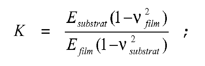
- Efilm : le module de Young de la
zone semi-conductrice 508 ; - Esubstrat : le module de Young du substrat ;
- νfilm : le coefficient de Poisson de la
zone semi-conductrice 508 ; - νfilm : le coefficient de Poisson du substrat ;
- Efilm: the Young's modulus of the
semiconductor zone 508; - Esubstrate: the Young's modulus of the substrate;
- νfilm: the Poisson's ratio of the
semiconducting zone 508; - νfilm: the Poisson's ratio of the substrate;
Afin de se ramener à un cas similaire à celui du modèle décrit dans les documents [1] et [2], on peut utiliser une autre approximation dans laquelle on remplace le bicouche formé par la couche isolante 5023 et la zone semi-conductrice 508 à base de Si par une seule couche 513 de SiO2 d'épaisseur équivalente eeq, de sorte que : eeq = e SiO2 + e Si≡SiO2, avec eSi≡SiO2 représente l'épaisseur équivalente d'un point de vue mécanique en SiO2 de la couche de zone semi-conductrice 508 (
La rigidité en flexion de ces deux couches ((eSi≡SiO2) et (eSi)) est de préférence constante.The bending stiffness of these two layers ((e Si≡SiO 2 ) and (e Si )) is preferably constant.
On obtient la relation suivante : 
Avec Ii représente le moment d'inertie de la couche i.With I i represents the moment of inertia of the layer i.
Sur la 
Les résultats représentés par cette courbe C100 concernent deux exemples de réalisation: un premier dans lequel l'épaisseur eSiO2 est de l'ordre de 16 nm avec une épaisseur eSi de l'ordre de 15 nanomètres et un deuxième exemple de réalisation dans lequel une épaisseur d'oxyde eSiO2 de l'ordre de 16 nm avec une épaisseur de Silicium eSi de l'ordre de 20 nm.The results represented by this curve C 100 relate to two exemplary embodiments: a first in which the thickness e SiO 2 is of the order of 16 nm with a thickness e Si of the order of 15 nanometers and a second embodiment in which a thickness of oxide e SiO2 of the order of 16 nm with a thickness of silicon e Si of the order of 20 nm.
Dans les deux cas, l'évolution de la contrainte moyenne en fonction du paramètre réduit (K.LZA/eeq) est presque identique et représenté par la courbe C100 sur la
Cette courbe C100 s'annule pour une valeur de : 
On peut ainsi obtenir une valeur de Lc correspondant au point auquel la courbe s'annule, pour n'importe quelle épaisseur de la couche isolante 5023 et de la zone semi-conductrice 508.It is thus possible to obtain a value of L c corresponding to the point at which the curve vanishes, for any thickness of the insulating layer 502 3 and the
Une combinaison des 2 méthodes précitées peut être éventuellement utilisée. On peut extraire des valeurs de longueur limite Lc pour différents couples (eSiO2 ; eSi), en extrapolant les courbes telles qu'illustrées sur les
Des résultats de cette comparaison sont donnés par exemple dans le tableau ci-dessous.
(nm)
(nm)
calculée
(nm)
(nm)
(nm)
calculated
(nm)
Les valeurs la longueur limite LC obtenues par les deux exemples de méthodes précités sont très proches l'une de l'autre.The limit length values L C obtained by the two examples of the aforementioned methods are very close to each other.
La
Une première zone semi-conductrice 3081, et une deuxième zone semi-conductrice 3082, ont une dimension critique L8 prévue inférieure à la longueur limite Lc/2 prédéterminée, dont des méthodes de détermination ont été données plus haut, et qui est déterminée en fonction notamment de l'épaisseur des zones semi-conductrices des couches 1023 et 1022.A first semiconductor zone 308 1 , and a second semiconductor zone 308 2 , have a critical dimension L 8 provided lower than the predetermined length Lc / 2, whose determination methods have been given above, and which is determined in particular as a function of the thickness of the semiconductor zones of the
Une troisième zone semi-conductrice 3091, et une quatrième zone semi-conductrice 3092, ont une dimension critique qui peut être également inférieure ou égale à la longueur limite Lc prédéterminée.A third semiconductor region 309 1 , and a fourth semiconductor zone 309 2 , have a critical dimension which may also be less than or equal to the predetermined length Lc.
Les zones semi-conductrices 3081, 3091, 3082, 3092, sont contraintes et reposent sur un bloc B10 gravé formé dans un empilement de couches minces comportant une couche précontrainte 1022. Des tranchées 310, 320, sont réalisées dans une partie de l'épaisseur de la couche précontrainte 1022, de part et d'autre du bloc B10 gravé. Les tranchées 310, 320, ont une profondeur supérieure à la dimension critique L8 des zones semi-conductrice 3081 et 3082. Une tranchée 320 est réalisée dans le prolongement d'un flanc de la zone semi-conductrice 3082. Une autre tranchée 310 est quant à elle réalisée dans le prolongement d'un flanc de la zone semi-conductrice 3081. Un transfert de la contrainte de la couche précontrainte 1022 au sommet du bloc B10 est mis en oeuvre dans les zones semi-conductrices 3081 et 3082.The semiconductor zones 308 1 , 309 1 , 308 2 , 309 2 are constrained and rest on an etched block B 10 formed in a stack of thin layers comprising a
Dans un cas par exemple où la couche précontrainte 1022 est contrainte en tension, les zones semi-conductrices 3081 et 3082 sont également contraintes en tension.In a case for example where the
Une zone semi-conductrice 3092 juxtaposée à la zone semi-conductrice 3082, est quant à elle située à une distance d d'au moins Lc/2 de la tranchée 320.A semiconductor zone 309 2 juxtaposed with the semiconductor zone 308 2 , for its part, is located at a distance d of at least Lc / 2 from the
Avec un tel agencement, dans un cas par exemple où la couche précontrainte 1022 est contrainte en tension, les zones semi-conductrices 1091 et 1092 sont contraintes en compression ou ont une contrainte moyenne correspondant à une contrainte en compression.With such an arrangement, in a case for example where the
Sur la
Le dispositif comprend des zones semi-conductrices 4081, 4082 contraintes selon un premier type de contrainte, par exemple une contrainte en tension, et des zones semi-conductrices 4091, 4092 contraintes selon un deuxième type de contrainte, par exemple une contrainte en compression.The device comprises semiconductor zones 408 1 , 408 2 constrained according to a first type of stress, for example a stress in tension, and semiconductor zones 409 1 , 409 2 constrained according to a second type of stress, for example a compressive stress.
Les zones semi-conductrices 4081, 4091, peuvent avoir été formées à partir d'une couche semi-conductrice pré-contrainte, et reposent sur un premier bloc Bloo formé d'un empilement de couches de matériau diélectrique 1021, 1022, 1023 dont au moins une couche 1022 précontrainte, par exemple en tension.The semiconductor zones 408 1 , 409 1 may have been formed from a pre-stressed semiconductor layer, and rest on a first block B 100 formed of a stack of layers of
Les zones semi-conductrices 4082, 4092 peuvent avoir été formées à partir de ladite couche semi-conductrice pré-contrainte, et reposent sur un deuxième bloc B200 formé dans l'empilement de couches de matériau diélectrique 1021, 1022, 1023.The semiconductor zones 408 2 , 409 2 may have been formed from said layer pre-stressed semiconductor, and rest on a second block B 200 formed in the stack of layers of
Les zones semi-conductrices 4081, 4082 sont prévus avec une dimension critique L8 < Lc/2, avec Lc la longueur limite dont des méthodes de détermination ont été données plus haut, et qui est fonction de l'épaisseur des zones semi-conductrices ainsi que de l'épaisseur respective des couches 1022 et 1023.The semiconductor zones 408 1 , 408 2 are provided with a critical dimension L 8 <Lc / 2, with Lc the limiting length of which determination methods have been given above, and which is a function of the thickness of the semi zones. as well as the respective thickness of the
Une tranchée 410 sépare le premier bloc B100 du deuxième bloc B200. Cette tranchée est réalisée dans le prolongement d'un flanc de la zone semi-conductrice 4081 et d'un flanc de la zone semi-conductrice 4082. Les zones semi-conductrices 4091 et 4092 sont quant à elles situées à une distance d d'au moins Lc/2 de la tranchée 410, afin de permettre de conférer à ces zones semi-conductrices 4091 et 4092, une contrainte de signe opposée à celle de la contrainte de la couche précontrainte et de la contrainte des zones semi-conductrices 4081, 4082.A
Sur la
Claims (14)
Applications Claiming Priority (1)
| Application Number | Priority Date | Filing Date | Title |
|---|---|---|---|
| FR0854946A FR2934085B1 (en) | 2008-07-21 | 2008-07-21 | METHOD FOR SIMULTANEOUS VOLTAGE CONVERSION AND COMPRESSION OF NMOS AND PMOS TRANSISTOR CHANNELS RESPECTIVELY |
Publications (3)
| Publication Number | Publication Date |
|---|---|
| EP2148373A2 true EP2148373A2 (en) | 2010-01-27 |
| EP2148373A3 EP2148373A3 (en) | 2013-06-12 |
| EP2148373B1 EP2148373B1 (en) | 2015-11-11 |
Family
ID=40377320
Family Applications (1)
| Application Number | Title | Priority Date | Filing Date |
|---|---|---|---|
| EP09165568.8A Active EP2148373B1 (en) | 2008-07-21 | 2009-07-15 | Method for applying simultaneous tensile and compressive stress to NMOS and PMOS transistor channels respectively |
Country Status (4)
| Country | Link |
|---|---|
| US (1) | US7951659B2 (en) |
| EP (1) | EP2148373B1 (en) |
| JP (1) | JP2010028121A (en) |
| FR (1) | FR2934085B1 (en) |
Families Citing this family (1)
| Publication number | Priority date | Publication date | Assignee | Title |
|---|---|---|---|---|
| US10147772B2 (en) | 2016-08-23 | 2018-12-04 | 3M Innovative Properties Company | Foldable OLED device with compatible flexural stiffness of layers |
Citations (3)
| Publication number | Priority date | Publication date | Assignee | Title |
|---|---|---|---|---|
| US7091095B2 (en) | 2003-03-15 | 2006-08-15 | International Business Machines Corporation | Dual strain-state SiGe layers for microelectronics |
| US7223994B2 (en) | 2004-06-03 | 2007-05-29 | International Business Machines Corporation | Strained Si on multiple materials for bulk or SOI substrates |
| US7262087B2 (en) | 2004-12-14 | 2007-08-28 | International Business Machines Corporation | Dual stressed SOI substrates |
Family Cites Families (6)
| Publication number | Priority date | Publication date | Assignee | Title |
|---|---|---|---|---|
| US6764908B1 (en) * | 2002-06-19 | 2004-07-20 | Advanced Micro Devices, Inc. | Narrow width CMOS devices fabricated on strained lattice semiconductor substrates with maximized NMOS and PMOS drive currents |
| US6878611B2 (en) * | 2003-01-02 | 2005-04-12 | International Business Machines Corporation | Patterned strained silicon for high performance circuits |
| US7034362B2 (en) * | 2003-10-17 | 2006-04-25 | International Business Machines Corporation | Double silicon-on-insulator (SOI) metal oxide semiconductor field effect transistor (MOSFET) structures |
| FR2872626B1 (en) * | 2004-07-05 | 2008-05-02 | Commissariat Energie Atomique | METHOD FOR CONTRAINDING A THIN PATTERN |
| US7125759B2 (en) * | 2005-03-23 | 2006-10-24 | Taiwan Semiconductor Manufacturing Co., Ltd. | Semiconductor-on-insulator (SOI) strained active areas |
| US7608489B2 (en) * | 2006-04-28 | 2009-10-27 | International Business Machines Corporation | High performance stress-enhance MOSFET and method of manufacture |
-
2008
- 2008-07-21 FR FR0854946A patent/FR2934085B1/en not_active Expired - Fee Related
-
2009
- 2009-07-15 EP EP09165568.8A patent/EP2148373B1/en active Active
- 2009-07-17 JP JP2009169396A patent/JP2010028121A/en active Pending
- 2009-07-17 US US12/505,161 patent/US7951659B2/en active Active
Patent Citations (3)
| Publication number | Priority date | Publication date | Assignee | Title |
|---|---|---|---|---|
| US7091095B2 (en) | 2003-03-15 | 2006-08-15 | International Business Machines Corporation | Dual strain-state SiGe layers for microelectronics |
| US7223994B2 (en) | 2004-06-03 | 2007-05-29 | International Business Machines Corporation | Strained Si on multiple materials for bulk or SOI substrates |
| US7262087B2 (en) | 2004-12-14 | 2007-08-28 | International Business Machines Corporation | Dual stressed SOI substrates |
Non-Patent Citations (2)
| Title |
|---|
| HU ET AL., APPL. PHYS., vol. 50, no. 7, July 1979 (1979-07-01), pages 4661 |
| HU ET AL., APPL. PHYS., vol. 70, no. 6, September 1991 (1991-09-01), pages R53 |
Also Published As
| Publication number | Publication date |
|---|---|
| FR2934085A1 (en) | 2010-01-22 |
| EP2148373A3 (en) | 2013-06-12 |
| EP2148373B1 (en) | 2015-11-11 |
| US20100041205A1 (en) | 2010-02-18 |
| FR2934085B1 (en) | 2010-09-03 |
| US7951659B2 (en) | 2011-05-31 |
| JP2010028121A (en) | 2010-02-04 |
Similar Documents
| Publication | Publication Date | Title |
|---|---|---|
| EP1947686B1 (en) | Device with MOSFET on SOI | |
| FR3060840A1 (en) | METHOD FOR MAKING A SEMICONDUCTOR DEVICE HAVING SELF-ALIGNED INTERNAL SPACERS | |
| FR3086456A1 (en) | METHOD FOR PRODUCING SUPERIMPOSED TRANSISTORS | |
| EP3502047A1 (en) | Nanowire field effect transistor with reduced contact resistance | |
| EP1638149B1 (en) | Method of manufacture of an heterostructure channel insulated gate field effect transistor | |
| EP2157603B1 (en) | Method for manufacturing localised GeOI structures, obtained by germanium enrichment | |
| FR3060841A1 (en) | METHOD FOR MAKING A SEMICONDUCTOR DEVICE HAVING SELF-ALIGNED INTERNAL SPACERS | |
| FR3060838A1 (en) | METHOD FOR PRODUCING A SEMICONDUCTOR DEVICE WITH A COMPRESSION-CONSTANT CHANNEL | |
| FR3060839A1 (en) | METHOD FOR PRODUCING A NANOFIL SEMICONDUCTOR DEVICE AND EXTERNAL AND INTERNAL SPACERS ALIGNED | |
| EP2835832A2 (en) | Improved method for producing doped areas and/or exerting a stress on the spacers of a transistor | |
| EP3502049B1 (en) | Method for manufacturing a semiconductor device comprising one or more nanostructures | |
| EP3511293A1 (en) | Method for manufacturing at least one field-effect transistor | |
| EP3026711B1 (en) | Improved method for inducing strain in a transistor channel using sacrificial source/drain regions and a gate replacement | |
| FR3073666B1 (en) | METHOD FOR MANUFACTURING FIELD EFFECT TRANSISTOR | |
| EP3376545B1 (en) | Transistor with structured source and drain regions and method for producing same | |
| FR3085536A1 (en) | CFET DEVICE AND METHOD FOR MANUFACTURING SUCH A DEVICE | |
| FR3057702A1 (en) | METHOD FOR MANUFACTURING A COILGROUND FIELD EFFECT TRANSISTOR | |
| FR3040538A1 (en) | TRANSISTOR MOS AND METHOD FOR MANUFACTURING THE SAME | |
| FR2991502A1 (en) | METHOD FOR MANUFACTURING INTEGRATED CIRCUIT HAVING INSULATION TRENCHES WITH SEPARATE DEPTHS | |
| EP1615271B1 (en) | Method of straining a thin film pattern | |
| EP2148373B1 (en) | Method for applying simultaneous tensile and compressive stress to NMOS and PMOS transistor channels respectively | |
| FR3067516A1 (en) | IMPLEMENTING SEMICONDUCTOR REGIONS IN AN ELECTRONIC CHIP | |
| EP2620984A1 (en) | Method for straining a thin pattern and method for manufacturing a transistor including said method | |
| EP3401953A1 (en) | Chip with strained nmos and pmos transistors | |
| FR2976401A1 (en) | ELECTRONIC COMPONENT COMPRISING A MOSFET TRANSISTOR ASSEMBLY AND METHOD FOR MANUFACTURING |
Legal Events
| Date | Code | Title | Description |
|---|---|---|---|
| PUAI | Public reference made under article 153(3) epc to a published international application that has entered the european phase |
Free format text: ORIGINAL CODE: 0009012 |
|
| AK | Designated contracting states |
Kind code of ref document: A2 Designated state(s): AT BE BG CH CY CZ DE DK EE ES FI FR GB GR HR HU IE IS IT LI LT LU LV MC MK MT NL NO PL PT RO SE SI SK SM TR |
|
| AX | Request for extension of the european patent |
Extension state: AL BA RS |
|
| RAP1 | Party data changed (applicant data changed or rights of an application transferred) |
Owner name: COMMISSARIAT A L'ENERGIE ATOMIQUE ET AUX ENERGIES |
|
| PUAL | Search report despatched |
Free format text: ORIGINAL CODE: 0009013 |
|
| AK | Designated contracting states |
Kind code of ref document: A3 Designated state(s): AT BE BG CH CY CZ DE DK EE ES FI FR GB GR HR HU IE IS IT LI LT LU LV MC MK MT NL NO PL PT RO SE SI SK SM TR |
|
| AX | Request for extension of the european patent |
Extension state: AL BA RS |
|
| RIC1 | Information provided on ipc code assigned before grant |
Ipc: H01L 29/10 20060101AFI20130506BHEP Ipc: H01L 21/8238 20060101ALI20130506BHEP |
|
| 17P | Request for examination filed |
Effective date: 20130827 |
|
| RBV | Designated contracting states (corrected) |
Designated state(s): AT BE BG CH CY CZ DE DK EE ES FI FR GB GR HR HU IE IS IT LI LT LU LV MC MK MT NL NO PL PT RO SE SI SK SM TR |
|
| RIC1 | Information provided on ipc code assigned before grant |
Ipc: H01L 21/84 20060101ALI20140226BHEP Ipc: H01L 29/10 20060101AFI20140226BHEP Ipc: H01L 21/8238 20060101ALI20140226BHEP |
|
| 17Q | First examination report despatched |
Effective date: 20140318 |
|
| GRAP | Despatch of communication of intention to grant a patent |
Free format text: ORIGINAL CODE: EPIDOSNIGR1 |
|
| INTG | Intention to grant announced |
Effective date: 20150601 |
|
| GRAS | Grant fee paid |
Free format text: ORIGINAL CODE: EPIDOSNIGR3 |
|
| GRAA | (expected) grant |
Free format text: ORIGINAL CODE: 0009210 |
|
| AK | Designated contracting states |
Kind code of ref document: B1 Designated state(s): AT BE BG CH CY CZ DE DK EE ES FI FR GB GR HR HU IE IS IT LI LT LU LV MC MK MT NL NO PL PT RO SE SI SK SM TR |
|
| REG | Reference to a national code |
Ref country code: GB Ref legal event code: FG4D Free format text: NOT ENGLISH |
|
| REG | Reference to a national code |
Ref country code: CH Ref legal event code: EP |
|
| REG | Reference to a national code |
Ref country code: IE Ref legal event code: FG4D Free format text: LANGUAGE OF EP DOCUMENT: FRENCH |
|
| REG | Reference to a national code |
Ref country code: AT Ref legal event code: REF Ref document number: 760833 Country of ref document: AT Kind code of ref document: T Effective date: 20151215 |
|
| REG | Reference to a national code |
Ref country code: DE Ref legal event code: R096 Ref document number: 602009034743 Country of ref document: DE |
|
| REG | Reference to a national code |
Ref country code: LT Ref legal event code: MG4D |
|
| REG | Reference to a national code |
Ref country code: NL Ref legal event code: MP Effective date: 20160211 |
|
| REG | Reference to a national code |
Ref country code: AT Ref legal event code: MK05 Ref document number: 760833 Country of ref document: AT Kind code of ref document: T Effective date: 20151111 |
|
| PG25 | Lapsed in a contracting state [announced via postgrant information from national office to epo] |
Ref country code: ES Free format text: LAPSE BECAUSE OF FAILURE TO SUBMIT A TRANSLATION OF THE DESCRIPTION OR TO PAY THE FEE WITHIN THE PRESCRIBED TIME-LIMIT Effective date: 20151111 Ref country code: NL Free format text: LAPSE BECAUSE OF FAILURE TO SUBMIT A TRANSLATION OF THE DESCRIPTION OR TO PAY THE FEE WITHIN THE PRESCRIBED TIME-LIMIT Effective date: 20151111 Ref country code: NO Free format text: LAPSE BECAUSE OF FAILURE TO SUBMIT A TRANSLATION OF THE DESCRIPTION OR TO PAY THE FEE WITHIN THE PRESCRIBED TIME-LIMIT Effective date: 20160211 Ref country code: IS Free format text: LAPSE BECAUSE OF FAILURE TO SUBMIT A TRANSLATION OF THE DESCRIPTION OR TO PAY THE FEE WITHIN THE PRESCRIBED TIME-LIMIT Effective date: 20160311 Ref country code: HR Free format text: LAPSE BECAUSE OF FAILURE TO SUBMIT A TRANSLATION OF THE DESCRIPTION OR TO PAY THE FEE WITHIN THE PRESCRIBED TIME-LIMIT Effective date: 20151111 Ref country code: IT Free format text: LAPSE BECAUSE OF FAILURE TO SUBMIT A TRANSLATION OF THE DESCRIPTION OR TO PAY THE FEE WITHIN THE PRESCRIBED TIME-LIMIT Effective date: 20151111 Ref country code: LT Free format text: LAPSE BECAUSE OF FAILURE TO SUBMIT A TRANSLATION OF THE DESCRIPTION OR TO PAY THE FEE WITHIN THE PRESCRIBED TIME-LIMIT Effective date: 20151111 |
|
| PG25 | Lapsed in a contracting state [announced via postgrant information from national office to epo] |
Ref country code: AT Free format text: LAPSE BECAUSE OF FAILURE TO SUBMIT A TRANSLATION OF THE DESCRIPTION OR TO PAY THE FEE WITHIN THE PRESCRIBED TIME-LIMIT Effective date: 20151111 Ref country code: SE Free format text: LAPSE BECAUSE OF FAILURE TO SUBMIT A TRANSLATION OF THE DESCRIPTION OR TO PAY THE FEE WITHIN THE PRESCRIBED TIME-LIMIT Effective date: 20151111 Ref country code: FI Free format text: LAPSE BECAUSE OF FAILURE TO SUBMIT A TRANSLATION OF THE DESCRIPTION OR TO PAY THE FEE WITHIN THE PRESCRIBED TIME-LIMIT Effective date: 20151111 Ref country code: PT Free format text: LAPSE BECAUSE OF FAILURE TO SUBMIT A TRANSLATION OF THE DESCRIPTION OR TO PAY THE FEE WITHIN THE PRESCRIBED TIME-LIMIT Effective date: 20160311 Ref country code: PL Free format text: LAPSE BECAUSE OF FAILURE TO SUBMIT A TRANSLATION OF THE DESCRIPTION OR TO PAY THE FEE WITHIN THE PRESCRIBED TIME-LIMIT Effective date: 20151111 Ref country code: GR Free format text: LAPSE BECAUSE OF FAILURE TO SUBMIT A TRANSLATION OF THE DESCRIPTION OR TO PAY THE FEE WITHIN THE PRESCRIBED TIME-LIMIT Effective date: 20160212 Ref country code: LV Free format text: LAPSE BECAUSE OF FAILURE TO SUBMIT A TRANSLATION OF THE DESCRIPTION OR TO PAY THE FEE WITHIN THE PRESCRIBED TIME-LIMIT Effective date: 20151111 |
|
| PG25 | Lapsed in a contracting state [announced via postgrant information from national office to epo] |
Ref country code: CZ Free format text: LAPSE BECAUSE OF FAILURE TO SUBMIT A TRANSLATION OF THE DESCRIPTION OR TO PAY THE FEE WITHIN THE PRESCRIBED TIME-LIMIT Effective date: 20151111 |
|
| REG | Reference to a national code |
Ref country code: FR Ref legal event code: PLFP Year of fee payment: 8 |
|
| REG | Reference to a national code |
Ref country code: DE Ref legal event code: R097 Ref document number: 602009034743 Country of ref document: DE |
|
| PG25 | Lapsed in a contracting state [announced via postgrant information from national office to epo] |
Ref country code: SK Free format text: LAPSE BECAUSE OF FAILURE TO SUBMIT A TRANSLATION OF THE DESCRIPTION OR TO PAY THE FEE WITHIN THE PRESCRIBED TIME-LIMIT Effective date: 20151111 Ref country code: SM Free format text: LAPSE BECAUSE OF FAILURE TO SUBMIT A TRANSLATION OF THE DESCRIPTION OR TO PAY THE FEE WITHIN THE PRESCRIBED TIME-LIMIT Effective date: 20151111 Ref country code: EE Free format text: LAPSE BECAUSE OF FAILURE TO SUBMIT A TRANSLATION OF THE DESCRIPTION OR TO PAY THE FEE WITHIN THE PRESCRIBED TIME-LIMIT Effective date: 20151111 Ref country code: DK Free format text: LAPSE BECAUSE OF FAILURE TO SUBMIT A TRANSLATION OF THE DESCRIPTION OR TO PAY THE FEE WITHIN THE PRESCRIBED TIME-LIMIT Effective date: 20151111 Ref country code: RO Free format text: LAPSE BECAUSE OF FAILURE TO SUBMIT A TRANSLATION OF THE DESCRIPTION OR TO PAY THE FEE WITHIN THE PRESCRIBED TIME-LIMIT Effective date: 20151111 |
|
| PLBE | No opposition filed within time limit |
Free format text: ORIGINAL CODE: 0009261 |
|
| STAA | Information on the status of an ep patent application or granted ep patent |
Free format text: STATUS: NO OPPOSITION FILED WITHIN TIME LIMIT |
|
| 26N | No opposition filed |
Effective date: 20160812 |
|
| PG25 | Lapsed in a contracting state [announced via postgrant information from national office to epo] |
Ref country code: SI Free format text: LAPSE BECAUSE OF FAILURE TO SUBMIT A TRANSLATION OF THE DESCRIPTION OR TO PAY THE FEE WITHIN THE PRESCRIBED TIME-LIMIT Effective date: 20151111 |
|
| PG25 | Lapsed in a contracting state [announced via postgrant information from national office to epo] |
Ref country code: BE Free format text: LAPSE BECAUSE OF NON-PAYMENT OF DUE FEES Effective date: 20160731 |
|
| REG | Reference to a national code |
Ref country code: CH Ref legal event code: PL |
|
| PG25 | Lapsed in a contracting state [announced via postgrant information from national office to epo] |
Ref country code: MC Free format text: LAPSE BECAUSE OF FAILURE TO SUBMIT A TRANSLATION OF THE DESCRIPTION OR TO PAY THE FEE WITHIN THE PRESCRIBED TIME-LIMIT Effective date: 20151111 |
|
| PG25 | Lapsed in a contracting state [announced via postgrant information from national office to epo] |
Ref country code: CH Free format text: LAPSE BECAUSE OF NON-PAYMENT OF DUE FEES Effective date: 20160731 Ref country code: LI Free format text: LAPSE BECAUSE OF NON-PAYMENT OF DUE FEES Effective date: 20160731 |
|
| REG | Reference to a national code |
Ref country code: IE Ref legal event code: MM4A |
|
| PG25 | Lapsed in a contracting state [announced via postgrant information from national office to epo] |
Ref country code: IE Free format text: LAPSE BECAUSE OF NON-PAYMENT OF DUE FEES Effective date: 20160715 |
|
| REG | Reference to a national code |
Ref country code: FR Ref legal event code: PLFP Year of fee payment: 9 |
|
| PG25 | Lapsed in a contracting state [announced via postgrant information from national office to epo] |
Ref country code: LU Free format text: LAPSE BECAUSE OF NON-PAYMENT OF DUE FEES Effective date: 20160715 |
|
| PG25 | Lapsed in a contracting state [announced via postgrant information from national office to epo] |
Ref country code: CY Free format text: LAPSE BECAUSE OF FAILURE TO SUBMIT A TRANSLATION OF THE DESCRIPTION OR TO PAY THE FEE WITHIN THE PRESCRIBED TIME-LIMIT Effective date: 20151111 Ref country code: HU Free format text: LAPSE BECAUSE OF FAILURE TO SUBMIT A TRANSLATION OF THE DESCRIPTION OR TO PAY THE FEE WITHIN THE PRESCRIBED TIME-LIMIT; INVALID AB INITIO Effective date: 20090715 |
|
| PG25 | Lapsed in a contracting state [announced via postgrant information from national office to epo] |
Ref country code: MT Free format text: LAPSE BECAUSE OF FAILURE TO SUBMIT A TRANSLATION OF THE DESCRIPTION OR TO PAY THE FEE WITHIN THE PRESCRIBED TIME-LIMIT Effective date: 20151111 Ref country code: TR Free format text: LAPSE BECAUSE OF FAILURE TO SUBMIT A TRANSLATION OF THE DESCRIPTION OR TO PAY THE FEE WITHIN THE PRESCRIBED TIME-LIMIT Effective date: 20151111 Ref country code: MK Free format text: LAPSE BECAUSE OF FAILURE TO SUBMIT A TRANSLATION OF THE DESCRIPTION OR TO PAY THE FEE WITHIN THE PRESCRIBED TIME-LIMIT Effective date: 20151111 |
|
| REG | Reference to a national code |
Ref country code: FR Ref legal event code: PLFP Year of fee payment: 10 |
|
| PG25 | Lapsed in a contracting state [announced via postgrant information from national office to epo] |
Ref country code: BG Free format text: LAPSE BECAUSE OF FAILURE TO SUBMIT A TRANSLATION OF THE DESCRIPTION OR TO PAY THE FEE WITHIN THE PRESCRIBED TIME-LIMIT Effective date: 20151111 |
|
| PGFP | Annual fee paid to national office [announced via postgrant information from national office to epo] |
Ref country code: GB Payment date: 20230724 Year of fee payment: 15 |
|
| PGFP | Annual fee paid to national office [announced via postgrant information from national office to epo] |
Ref country code: FR Payment date: 20230724 Year of fee payment: 15 Ref country code: DE Payment date: 20230720 Year of fee payment: 15 |