EP2141706A1 - Memory card adaptor - Google Patents
Memory card adaptor Download PDFInfo
- Publication number
- EP2141706A1 EP2141706A1 EP08290660A EP08290660A EP2141706A1 EP 2141706 A1 EP2141706 A1 EP 2141706A1 EP 08290660 A EP08290660 A EP 08290660A EP 08290660 A EP08290660 A EP 08290660A EP 2141706 A1 EP2141706 A1 EP 2141706A1
- Authority
- EP
- European Patent Office
- Prior art keywords
- card
- connector
- interface circuit
- circuit
- switch
- Prior art date
- Legal status (The legal status is an assumption and is not a legal conclusion. Google has not performed a legal analysis and makes no representation as to the accuracy of the status listed.)
- Withdrawn
Links
Images
Classifications
-
- G—PHYSICS
- G11—INFORMATION STORAGE
- G11C—STATIC STORES
- G11C5/00—Details of stores covered by group G11C11/00
- G11C5/02—Disposition of storage elements, e.g. in the form of a matrix array
- G11C5/04—Supports for storage elements, e.g. memory modules; Mounting or fixing of storage elements on such supports
-
- G—PHYSICS
- G06—COMPUTING; CALCULATING OR COUNTING
- G06K—GRAPHICAL DATA READING; PRESENTATION OF DATA; RECORD CARRIERS; HANDLING RECORD CARRIERS
- G06K19/00—Record carriers for use with machines and with at least a part designed to carry digital markings
- G06K19/06—Record carriers for use with machines and with at least a part designed to carry digital markings characterised by the kind of the digital marking, e.g. shape, nature, code
- G06K19/067—Record carriers with conductive marks, printed circuits or semiconductor circuit elements, e.g. credit or identity cards also with resonating or responding marks without active components
- G06K19/07—Record carriers with conductive marks, printed circuits or semiconductor circuit elements, e.g. credit or identity cards also with resonating or responding marks without active components with integrated circuit chips
- G06K19/077—Constructional details, e.g. mounting of circuits in the carrier
- G06K19/07737—Constructional details, e.g. mounting of circuits in the carrier the record carrier consisting of two or more mechanically separable parts
- G06K19/07739—Constructional details, e.g. mounting of circuits in the carrier the record carrier consisting of two or more mechanically separable parts comprising a first part capable of functioning as a record carrier on its own and a second part being only functional as a form factor changing part, e.g. SIM cards type ID 0001, removably attached to a regular smart card form factor
Definitions
- the invention relates to a memory card adapter. More particularly, the invention relates to an adapter for connecting a second device to a memory card port in addition to a memory card.
- SD Secure Digital
- SDIO Secure Digital Input Output device
- SD-MCE Secure Digital - Mobile Commerce Extension
- the invention proposes an adapter device for connecting two electronic devices to the same port.
- the host device is addressed to a single device that makes it possible, on the one hand, to perform an electronic function and, on the other hand, mass storage.
- the invention provides a solution for controlling two devices on a single port that allows the connection of a single device.
- the invention is an adapter device that includes a first connector, a second connector, a switch, and a device interface circuit.
- the first connector is intended to be connected to a host device receiving said adapter device.
- the second connector is for receiving a memory card.
- the switch connects the first connector to the second connector.
- the device interface circuit is connected to the first connector and controls the switch to open or close it according to the commands that arrive at the first connector.
- the device comprises an application circuit connected to the device interface circuits.
- the device includes a host interface circuit connected to the second connector for communicating with the memory card.
- the device interface circuit and the host interface circuit are interconnected to exchange data and to develop common characteristics taking into account card characteristics and device characteristics.
- the device interface circuit closes the switch when a command is received on the first connector and keeps it closed to let the card answer when the command is to the card. In the absence of a card, the device interface circuit responds to all commands. The device interface circuit closes the switch when a command is received on the first connector and opens the switch to block the response of the card when the command is to the application circuit.
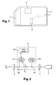
- the figure 1 shows a preferred embodiment of an adapter according to the invention.
- the adapter 1 is here made in the format of an SD memory card.
- the adapter 1 comprises a first connector 2 in the format of an SD card connector.
- the adapter 1 comprises a housing for receiving a memory card 3 in microSD format which is connected via a second connector 4.
- the adapter 1 comprises a chip 5 connected to the first and second connectors 2 and 4.
- the chip 5 contains the electronic circuits of the adapter 1.
- the electronic circuits of the adapter 1 are all placed on a single chip, however, it is possible to use circuits made on several chips.
- the figure 2 functionally details the electronic circuits contained in the chip 5.
- the first and second connectors 2 and 4 are connected to the chip, respectively by a first and a second bus 20 and 40 containing as many connectors as there are contacts for an SD card connector. For the sake of clarity of drawing, only one wire is shown.
- the first and second buses are interconnected via a first switch S1 which consists of a switch assembly for contacting or open circuit each conductor bus 20 and 40.
- the switch S1 allows either to ensure a direct connection between the two connectors 2 and 4, or to isolate them from one another.
- a device interface circuit 51 is connected to the first bus 20.
- the device interface circuit 51 is a circuit for communicating with a host connected to the first connector 2. It is the user interface circuit that provides the management of the communication protocol for an application circuit 52.
- the application circuit 52 may be of any type, for example an SD-MCE type pay television management circuit. Other application circuits are conceivable; the circuit 52 may be a modem having another connection, a chip card reader compliant with the ISO7816 standard, or any other type of application that can be connected by an SD bus.
- the device interface circuit 51 analyzes all the commands exchanged at the first connector 2. However, this interface circuit does not respond to all the commands. Indeed, some commands are processed directly by the card 3.
- the interface circuit is further connected to the switch S1 to control it and determine if the card responds directly or not, depending on the orders observed.
- a host interface circuit 53 is connected, on the one hand, to the second bus 40 and, on the other hand, to the device interface circuit 51.
- the host interface circuit 53 makes it possible to control the card 3 when the switch S1 is open.
- the link between the host interface circuit 53 is connected to the device interface circuit 51 to be able to integrate information from the card 3 to information returned by the device interface device 51.
- the adapter 1 is presented to the host that receives it as a single device integrating both the characteristics of the application circuit 52 and the characteristics of the card 3. During this start-up phase, the same principle that previously explained is implemented, however, it should also anticipate some control of the host device with respect to the card.
- the Vdd is chosen to correspond to both the card 3 and the adapter 1
- the maximum currents are added
- the transfer rates are determined as a function of the slower between the card and the device interface circuit 51, etc.
- the CSD and OCR registers are reconstituted to present characteristics which are compatible with both card 3 and adapter 1.
- the CID register it is also necessary to aggregate the data.
- the manufacturer of the adapter and the card are not the same.
- the card 3 is removable relative to the adapter and the identification information is not the same whether the card is present or not.
- the adapter must memorize this information because the address provided by the card can also be used to address the application circuit.
- the switching circuit 54 detects the command Cmd4 on the bus 20 and keeps the switch S1 closed.
- the interface circuit 51 does not respond and leaves switch S1 closed so that the card responds directly.
- the host interface circuit 53 intercepts the response and transmits the data or data to the circuit. device interface 51 for storage in the relevant register.
- the switch S1 is opened as soon as the completeness the order is placed.
- the host interface circuit receives the possible response from the card 3.
- the device interface circuit 51 will respond, possibly taking into account the response of the card 3.
- the device interface circuit 51 When the device interface circuit 51 has finished responding, it closes the card. S1 switch so that the card can receive the following command.
- the SD host When the SD host wants to send one or more commands to the application circuit 52, it must use an extended command set. For this it sends a command, for example Cmd6, which is not supported by the card 3.
- a command for example Cmd6, which is not supported by the card 3.
- the switching circuit 54 detects this command Cmd6, then it opens the switch S1.
- the card 3, having received the command Cmd6, can answer that it does not support this command but its answer is not transmitted to the host SD.
- the response is made by the interface circuit 51 and then the switch S1 is closed so that the card can receive the following command in case it is intended for it.
- the adapter In the event of a power failure, the adapter re-performs the start-up phase.
- the adapter without the card 3.
- the card will never respond to the commands that are sent. If we take the previous table, this results in no response to commands Cmd8 and Acmd41.
- the response to the command Cmd8 is optional and therefore does not mean the absence of the card.
- the absence of the OCR response within a specified time means that there is no card 3 and thus the device interface 51 can respond with its own OCR register immediately after the next Acmd41 command.
- the application circuit 52 it is possible for the application circuit 52 to store information on the card 3, in which case the switch S1 must be opened and the card 3 to be addressed with the aid of 53. If during this use of the card 3, the SD host sends a command to the card, the device interface circuit will respond that the card is not available using the "busy” response. ".
- An SDIO format card may have a larger portion than an SD card and it is possible to replace the microSD card 3 with any other SD or miniSD card format.
- the application circuit 52 can be of any type supported by the SDIO standard and it is possible that the application circuit 52 has a connection to another external circuit.
- the chip 5 corresponds to a set of electronic circuits made on a single chip. It is obvious that, depending on the type of application implemented by the adapter, the electronic circuits can be made on several separate chips.
Abstract
Description
L'invention se rapporte un adaptateur de carte mémoire. Plus particulièrement l'invention se rapporte à un adaptateur permettant de connecter un deuxième dispositif sur un port de carte mémoire en plus d'une carte à mémoire.The invention relates to a memory card adapter. More particularly, the invention relates to an adapter for connecting a second device to a memory card port in addition to a memory card.
La possibilité d'avoir de grande capacité de stockage sur des mémoires de type Flash a développé le marché des cartes à mémoire. Les cartes à mémoires sont conforment à différents standards parmi lesquels on peut citer le standard SD (Secure Digital). Le Standard SD, comme tous les standards de cartes à mémoire, définit un format de carte, un type de connecteur et un protocole de communication entre un dispositif hôte destiné à recevoir la carte SD et la carte SD. Par standard SD, il faut comprendre dans ce document les publications faites par la SD Card Association et incluant les documents de définition de « SD memory card, Physical layer specification », « SDI-fC memory card », « miniSD card », « microSD card », « SDIO card », et « SD host controller spécification », Certains standards de carte à mémoire utilise en outre un protocole de communication étendu qui permet d'utiliser des instructions supplémentaires pour utiliser des dispositifs différents des cartes à mémoires. Notamment, le standard SD comporte une extension de jeu de commandes appelée SDIO (pour Secure Digital Input Output device). Grâce à cette extension SDIO, il est possible de connecter au dispositif hôte des diverses interfaces d'entrée/sortie.The possibility of having large storage capacity on Flash type memories has developed the memory card market. The memory cards conform to different standards, among which the SD (Secure Digital) standard. Standard SD, like all standard smart cards, defines a card format, a connector type, and a communication protocol between a host device to receive the SD card and the SD card. By standard SD, it is necessary to understand in this document the publications made by the SD Card Association and including the definition documents of "SD memory card, Physical layer specification", "SDI-fC memory card", "miniSD card", "microSD" card "," SDIO card ", and" SD host controller specification ", Some smart card standards also use an extended communication protocol that allows you to use additional instructions to use different devices from memory cards. In particular, the SD standard includes a command set extension called SDIO (Secure Digital Input Output device). Thanks to this SDIO extension, it is possible to connect to the host device various input / output interfaces.
Dans le monde des cartes SD, il est connu d'utiliser une carte de type SDIO pour valider des services autre que du stockage de données. On parle aussi de SD-MCE (Secure Digital - Mobile Commerce Extension). Grâce à ce type de carte, il est possible d'avoir accès à des services autre que du stockage, par exemple de la télévision à péage, sur des appareils mobiles tels que, par exemple des téléphones portables ou des petits ordinateurs portables.In the world of SD cards, it is known to use an SDIO type card to validate services other than data storage. We are also talking about SD-MCE (Secure Digital - Mobile Commerce Extension). With this type of card, it is possible to have access to services other than storage, for example pay-TV, on mobile devices such as, for example, mobile phones or small laptops.
Cependant, les appareils mobiles disposent d'un seul port de carte à mémoire et l'évolution de ces appareils ne va pas dans le sens de rajouter un deuxième port. Ainsi un utilisateur désireux d'avoir un service de télévision à péage sur son téléphone ne peux garder en même temps une carte à mémoire destinée à faire du stockage de masse. Le fait qu'un utilisateur doive changer de carte en fonction de l'utilisation n'est pas souhaitable car le changement de carte oblige de ne pouvoir accéder la mémoire de masse que si l'on n'utilise pas le service de télévision. Or un utilisateur peut désirer stocker des informations pendant l'utilisation du service de télévision. En outre, le standard SD ne prévoit pas de pouvoir connecter en parallèle deux dispositifs sur un même port.However, mobile devices have only one memory card slot and the evolution of these devices is not going to add a second port. Thus a user wishing to have a pay-TV service on his phone can not keep at the same time a memory card for mass storage. The fact that a user has to change cards according to the use is not desirable because the change of card makes it impossible to access the mass memory if one does not use the television service. However, a user may wish to store information while using the television service. In addition, the SD standard does not provide the ability to connect two devices in parallel on the same port.
L'invention propose un dispositif adaptateur permettant de connecter sur un même port deux dispositifs électroniques. Ainsi le dispositif hôte s'adresse à un unique dispositif qui permet de réaliser d'une part une fonction électronique et d'autre part du stockage de masse. Plus généralement, l'invention apporte une solution pour piloter deux dispositifs sur un unique port qui autorise la connexion d'un unique dispositif.The invention proposes an adapter device for connecting two electronic devices to the same port. Thus, the host device is addressed to a single device that makes it possible, on the one hand, to perform an electronic function and, on the other hand, mass storage. More generally, the invention provides a solution for controlling two devices on a single port that allows the connection of a single device.
Ainsi, l'invention est un dispositif adaptateur qui comporte un premier connecteur, un deuxième connecteur, un interrupteur et un circuit d'interface de dispositif. Le premier connecteur est destiné à être connecté à un dispositif hôte recevant ledit dispositif adaptateur. Le deuxième connecteur est destiné à recevoir une carte à mémoire. L'interrupteur relie le premier connecteur au deuxième connecteur. Le circuit d'interface de dispositif est relié au premier connecteur et commande l'interrupteur pour l'ouvrir ou le fermer en fonction des commandes qui arrivent sur le premier connecteur.Thus, the invention is an adapter device that includes a first connector, a second connector, a switch, and a device interface circuit. The first connector is intended to be connected to a host device receiving said adapter device. The second connector is for receiving a memory card. The switch connects the first connector to the second connector. The device interface circuit is connected to the first connector and controls the switch to open or close it according to the commands that arrive at the first connector.
Préférentiellement, le dispositif comporte un circuit applicatif relié au circuits d'interface de dispositif. Le dispositif comporte un circuit d'interface hôte relié au deuxième connecteur pour communiquer avec la carte à mémoire. Le circuit d'interface de dispositif et le circuit d'interface hôte sont reliés entre eux pour échanger des données et élaborer des caractéristiques communes prenant en compte des caractéristiques de la carte et des caractéristiques propres au dispositif.Preferably, the device comprises an application circuit connected to the device interface circuits. The device includes a host interface circuit connected to the second connector for communicating with the memory card. The device interface circuit and the host interface circuit are interconnected to exchange data and to develop common characteristics taking into account card characteristics and device characteristics.
Selon un mode de réalisation particulier, le circuit d'interface de dispositif ferme l'interrupteur lorsqu'une commande est reçue sur le premier connecteur et le maintient fermé pour laisser passer la réponse de la carte lorsque la commande est à destination de la carte. En l'absence de carte, le circuit d'interface de dispositif répond à toutes les commandes. Le circuit d'interface de dispositif ferme l'interrupteur lorsqu'une commande est reçue sur le premier connecteur et ouvre l'interrupteur pour bloquer la réponse de la carte lorsque la commande est à destination du circuit applicatif.According to a particular embodiment, the device interface circuit closes the switch when a command is received on the first connector and keeps it closed to let the card answer when the command is to the card. In the absence of a card, the device interface circuit responds to all commands. The device interface circuit closes the switch when a command is received on the first connector and opens the switch to block the response of the card when the command is to the application circuit.
L'invention sera mieux comprise, et d'autres particularités et avantages apparaîtront à la lecture de la description qui va suivre, la description faisant référence aux dessins annexés, parmi lesquels :
- la
figure 1 représente un mode de réalisation préféré d'un adaptateur au format carte SD, - la
figure 2 représente un schéma fonctionnel de l'invention,
- the
figure 1 represents a preferred embodiment of an SD card format adapter, - the
figure 2 represents a block diagram of the invention,
La
La
Les premier et deuxième bus sont reliés entre eux par l'intermédiaire d'un premier interrupteur S1 qui est constitué d'un ensemble d'interrupteur permettant de mettre en contact ou en circuit ouvert chaque conducteur des bus 20 et 40. L'interrupteur S1 permet ainsi soit d'assurer une liaison directe entre les deux connecteurs 2 et 4, soit de les isoler l'un de l'autre.The first and second buses are interconnected via a first switch S1 which consists of a switch assembly for contacting or open circuit each
Un circuit d'interface de dispositif 51 est relié au premier bus 20. Le circuit d'interface de dispositif 51 est un circuit destiné à communiquer avec un hôte connecté au premier connecteur 2. C'est le circuit d'interface utilisateur qui assure la gestion du protocole de communication pour un circuit d'application 52. Le circuit d'application 52 peut être de n'importe quel type, par exemple un circuit de gestion de télévision à péage de type SD-MCE. D'autres circuits d'applications sont envisageables ; le circuit 52 peut être un modem disposant d'une autre connexion, un lecteur de carte à puce conforme à la norme ISO7816, ou encore n'importe quel autre type d'application pouvant être relié par un bus SD.A
Le circuit d'interface de dispositif 51 analyse toutes les commandes échangées au niveau du premier connecteur 2. Cependant ce circuit d'interface ne répond pas à toutes les commandes. En effet, certaines commandes sont traitées directement par la carte 3. Le circuit d'interface est en outre relié à l'interrupteur S1 pour le commander et déterminer si la carte répond directement ou pas, en fonction des commandes observées.The
Un circuit d'interface hôte 53 est relié, d'une part, au deuxième bus 40 et, d'autre part, au circuit d'interface de dispositif 51. Le circuit d'interface hôte 53 permet de contrôler la carte 3 lorsque l'interrupteur S1 est ouvert. La liaison entre le circuit interface hôte 53 est relié au circuit interface de dispositif 51 pour pouvoir intégrer des informations provenant de la carte 3 à des informations retournées par le dispositif interface de dispositif 51.A
Au démarrage, l'adaptateur 1 se présente à l'hôte qui le reçoit comme un unique dispositif intégrant à la fois les caractéristiques propres au circuit d'application 52 et les caractéristiques de la carte 3. Durant cette phase de démarrage, le même principe que précédemment expliqué est mis en oeuvre, toutefois, il convient également d'anticiper certaine commande du dispositif hôte vis à vis de la carte.At startup, the adapter 1 is presented to the host that receives it as a single device integrating both the characteristics of the
Le tableau ci-après détaille chronologiquement les échanges de commandes et réponses lors de la phase de démarrage ou d'initialisation. Les commandes et réponses indiquées dans le tableau ainsi que les registres d'état mentionnés sont définis dans le standard SD auquel l'homme du métier peut se référer pour plus de détail.
II est à noter que la concaténation des informations dans les registres CSD et OCR du circuit d'interface de dispositif 51 est faite de manière intelligente : Le Vdd est choisi pour correspondre à la fois à la carte 3 et à l'adaptateur 1, les courants maximum sont additionnés les vitesses de transfert sont déterminées en fonction du plus lent entre la carte et le circuit d'interface de dispositif 51, etc... Les registres CSD et OCR sont reconstitués pour présenter des caractéristiques qui sont compatibles à la fois avec la carte 3 et l'adaptateur 1.It should be noted that the concatenation of the information in the CSD and OCR registers of the
Pour le registre CID, il convient également de faire une agrégation des données. Le fabricant de l'adaptateur et de la carte ne sont pas les mêmes. En outre la carte 3 est amovible par rapport à l'adaptateur et l'information d'identification n'est pas la même suivant que la carte soit présente ou pas.For the CID register, it is also necessary to aggregate the data. The manufacturer of the adapter and the card are not the same. In addition, the
En ce qui concerne le contenu du registre RCA, l'adaptateur doit mémoriser cette information car l'adresse fournie par la carte peut également servir à adresser le circuit applicatif.Regarding the contents of the RCA register, the adapter must memorize this information because the address provided by the card can also be used to address the application circuit.
A la fin de la phase de démarrage, le circuit de commutation 54 détecte la commande Cmd4 sur le bus 20 et maintient l'interrupteur S1 fermé. Ainsi, lorsque l'hôte SD envoie des commandes de lecture ou d'écriture ou d'autres commandes uniquement à destination de la carte 3, ces commandes sont directement reçues par la carte 3, le circuit d'interface 51 ne répond pas et laisse l'interrupteur S1 fermé de sorte que la carte répond directement. Eventuellement, si la réponse concerne un état de la carte qui peut-être utilisé dans un registre d'état du dispositif d'interface de dispositif 51, alors le circuit interface hôte 53 intercepte la réponse et transmet la ou les données au circuit d'interface de dispositif 51 pour mémorisation dans le registre concerné.At the end of the start-up phase, the switching circuit 54 detects the command Cmd4 on the
Si la commande reçue n'est pas une commande uniquement en rapport avec la carte 3 alors l'interrupteur S1 est ouvert dès que l'intégralité de la commande est passée. Le circuit interface hôte reçoit l'éventuelle réponse de la carte 3. Le circuit interface de dispositif 51 répondra, éventuellement en tenant compte de la réponse de la carte 3. Lorsque le circuit interface de dispositif 51 a fini de répondre, il referme l'interrupteur S1 se sorte que la carte puisse recevoir la commande suivante.If the received command is not a command only in connection with the
Lorsque l'hôte SD veut envoyer une ou plusieurs commandes à destination du circuit d'application 52, il doit utiliser un jeu de commandes étendu. Pour cela il envoie une commande, par exemple Cmd6, qui n'est pas supportée par la carte 3. Lorsque le circuit de commutation 54 détecte cette commande Cmd6, alors il ouvre le l'interrupteur S1. La carte 3, ayant reçu la commande Cmd6, peut répondre qu'elle ne supporte pas cette commande mais sa réponse n'est pas transmise à l'hôte SD. La réponse est faite par le circuit d'interface 51 puis l'interrupteur S1 est refermé pour que la carte puisse recevoir la commande suivante au cas où elle lui soit destinée.When the SD host wants to send one or more commands to the
En cas de coupure d'alimentation, l'adaptateur ré-effectue la phase de démarrage.In the event of a power failure, the adapter re-performs the start-up phase.
Il est également possible d'utiliser l'adaptateur sans la carte 3. Dans ce cas, lors de la phase de démarrage la carte ne répondra jamais aux commandes qui sont envoyées. Si l'on reprend le tableau précédent, cela se traduit par une absence de réponse aux commandes Cmd8 et Acmd41. La réponse à la commande Cmd8 est optionnelle et donc ne signifie pas l'absence de la carte. Par contre, l'absence de la réponse OCR dans un délai déterminé signifie qu'il n'y a pas de carte 3 et donc l'interface de dispositif 51 peut répondre avec son propre registre OCR immédiatement après la prochaine commande Acmd41.It is also possible to use the adapter without the
Dans une variante, il est possible que le circuit d'application 52 ait besoin de stocker des informations sur la carte 3, Dans ce cas, il convient d'ouvrir l'interrupteur S1 et d'adresser la carte 3 à l'aide de l'interface hôte 53. Si pendant cette utilisation de la carte 3, l'hôte SD envoie une commande à destination de la carte, le circuit d'interface de dispositif répondra que la carte n'est pas disponible en utilisant la réponse « busy ».In a variant, it is possible for the
L'exemple précédemment décrit fait référence à un adaptateur au format d'une carte SD et recevant une carte microSD. Ces facteurs de formes peuvent être modifier. Une carte au format SDIO peut disposer d'une partie de taille plus importante qu'une carte SD et il est possible de remplacer la carte microSD 3 par tout autre format de carte SD ou miniSD.The example described above refers to an adapter in the format of an SD card and receiving a microSD card. These factors forms can be modify. An SDIO format card may have a larger portion than an SD card and it is possible to replace the
Comme précédemment indiqué également le circuit d'application 52 peut être de tout type supporté par le standard SDIO et il est possible que le circuit d'application 52 dispose d'une connexion vers un autre circuit externe.As previously indicated also the
Toujours dans ce mode de réalisation préféré, la puce 5 correspond à un ensemble de circuits électroniques réalisés sur une seule puce. II est évident que, suivant le type d'application mis en oeuvre par l'adaptateur, les circuits électroniques peuvent être réalisés sur plusieurs puces distinctes.Still in this preferred embodiment, the
Le problème posé ainsi que le mode de réalisation préféré sont relatif au standard SD. Toutefois, il existe d'autre standard de carte mémoire qui ont des caractéristiques similaires au standard 5D et pour lesquels le même problème se pose et ou une solution de même nature est applicable. A partir du moment où un standard de carte mémoire autorise la communication avec autre chose qu'une carte à mémoire et que le protocole de communication n'autorise la communication qu'avec un seul dispositif, l'utilisation d'un adaptateur, de même nature est utilisable. Il conviendra d'utiliser d'autres commandes propres au standard utilisé.The problem as well as the preferred embodiment are relative to the SD standard. However, there are other standard memory cards that have similar characteristics to the 5D standard and for which the same problem arises and or a solution of the same nature is applicable. From the moment a standard memory card allows communication with something other than a memory card and the communication protocol allows communication with only one device, the use of an adapter, as well as nature is usable. Other commands specific to the standard used should be used.
Claims (9)
Priority Applications (6)
| Application Number | Priority Date | Filing Date | Title |
|---|---|---|---|
| EP08290660A EP2141706A1 (en) | 2008-07-04 | 2008-07-04 | Memory card adaptor |
| EP09772485A EP2304729B1 (en) | 2008-07-04 | 2009-07-01 | Memory card adapter |
| US13/001,387 US8602314B2 (en) | 2008-07-04 | 2009-07-01 | Memory card adapter |
| JP2011515455A JP5501351B2 (en) | 2008-07-04 | 2009-07-01 | Memory card adapter |
| PCT/EP2009/058286 WO2010000785A1 (en) | 2008-07-04 | 2009-07-01 | Memory card adapter |
| CN200980134094.9A CN102144262B (en) | 2008-07-04 | 2009-07-01 | Memory card adapter |
Applications Claiming Priority (1)
| Application Number | Priority Date | Filing Date | Title |
|---|---|---|---|
| EP08290660A EP2141706A1 (en) | 2008-07-04 | 2008-07-04 | Memory card adaptor |
Publications (1)
| Publication Number | Publication Date |
|---|---|
| EP2141706A1 true EP2141706A1 (en) | 2010-01-06 |
Family
ID=39817079
Family Applications (2)
| Application Number | Title | Priority Date | Filing Date |
|---|---|---|---|
| EP08290660A Withdrawn EP2141706A1 (en) | 2008-07-04 | 2008-07-04 | Memory card adaptor |
| EP09772485A Not-in-force EP2304729B1 (en) | 2008-07-04 | 2009-07-01 | Memory card adapter |
Family Applications After (1)
| Application Number | Title | Priority Date | Filing Date |
|---|---|---|---|
| EP09772485A Not-in-force EP2304729B1 (en) | 2008-07-04 | 2009-07-01 | Memory card adapter |
Country Status (5)
| Country | Link |
|---|---|
| US (1) | US8602314B2 (en) |
| EP (2) | EP2141706A1 (en) |
| JP (1) | JP5501351B2 (en) |
| CN (1) | CN102144262B (en) |
| WO (1) | WO2010000785A1 (en) |
Families Citing this family (4)
| Publication number | Priority date | Publication date | Assignee | Title |
|---|---|---|---|---|
| TWM423936U (en) * | 2011-09-13 | 2012-03-01 | Tyco Electronics Holdings Bermuda No 7 Ltd | Smartcard connector with RFID module |
| EP2711864A1 (en) * | 2012-09-25 | 2014-03-26 | Gemalto SA | Method of configuring two wireless devices for mutual communication |
| FR3038423B1 (en) * | 2015-06-30 | 2018-07-20 | Idemia France | ELECTRONIC ENTITY AND METHOD IMPLEMENTED IN SUCH AN ELECTRONIC ENTITY |
| TWI640870B (en) * | 2017-03-17 | 2018-11-11 | 新唐科技股份有限公司 | Hub |
Citations (3)
| Publication number | Priority date | Publication date | Assignee | Title |
|---|---|---|---|---|
| US5936226A (en) * | 1995-09-27 | 1999-08-10 | Intel Corporation | Mass storage device adapter for smart cards |
| WO2002005102A1 (en) * | 2000-07-06 | 2002-01-17 | Onspec Electronic, Inc. | Flashtoaster for reading several types of flash memory cards with or without a pc |
| US20060164891A1 (en) * | 1999-05-11 | 2006-07-27 | Socket Communications, Inc. | Removable modules with external I/O flexibility via an integral second-level removable slot |
Family Cites Families (6)
| Publication number | Priority date | Publication date | Assignee | Title |
|---|---|---|---|---|
| JP3953832B2 (en) * | 2002-02-22 | 2007-08-08 | 株式会社村田製作所 | Interface card for media |
| JP3815400B2 (en) * | 2002-08-08 | 2006-08-30 | ソニー株式会社 | Adapter device |
| JP4723381B2 (en) * | 2004-01-06 | 2011-07-13 | dブロード株式会社 | SDIO card device with bus share adapter function |
| US20070132733A1 (en) * | 2004-06-08 | 2007-06-14 | Pranil Ram | Computer Apparatus with added functionality |
| US20070001017A1 (en) * | 2005-06-29 | 2007-01-04 | Moshe Nuri | Reduced complexity multifunction expansion card and method of operating the same |
| JP4640451B2 (en) * | 2008-06-06 | 2011-03-02 | ソニー株式会社 | Contact / non-contact composite IC card, communication method, program, and communication system |
-
2008
- 2008-07-04 EP EP08290660A patent/EP2141706A1/en not_active Withdrawn
-
2009
- 2009-07-01 US US13/001,387 patent/US8602314B2/en not_active Expired - Fee Related
- 2009-07-01 EP EP09772485A patent/EP2304729B1/en not_active Not-in-force
- 2009-07-01 WO PCT/EP2009/058286 patent/WO2010000785A1/en active Application Filing
- 2009-07-01 JP JP2011515455A patent/JP5501351B2/en not_active Expired - Fee Related
- 2009-07-01 CN CN200980134094.9A patent/CN102144262B/en not_active Expired - Fee Related
Patent Citations (3)
| Publication number | Priority date | Publication date | Assignee | Title |
|---|---|---|---|---|
| US5936226A (en) * | 1995-09-27 | 1999-08-10 | Intel Corporation | Mass storage device adapter for smart cards |
| US20060164891A1 (en) * | 1999-05-11 | 2006-07-27 | Socket Communications, Inc. | Removable modules with external I/O flexibility via an integral second-level removable slot |
| WO2002005102A1 (en) * | 2000-07-06 | 2002-01-17 | Onspec Electronic, Inc. | Flashtoaster for reading several types of flash memory cards with or without a pc |
Also Published As
| Publication number | Publication date |
|---|---|
| JP2011526713A (en) | 2011-10-13 |
| US8602314B2 (en) | 2013-12-10 |
| JP5501351B2 (en) | 2014-05-21 |
| US20110201233A1 (en) | 2011-08-18 |
| CN102144262A (en) | 2011-08-03 |
| CN102144262B (en) | 2014-05-21 |
| EP2304729A1 (en) | 2011-04-06 |
| EP2304729B1 (en) | 2012-09-05 |
| WO2010000785A1 (en) | 2010-01-07 |
Similar Documents
| Publication | Publication Date | Title |
|---|---|---|
| US7114030B2 (en) | System, apparatus and method for sharing media | |
| EP1855229B1 (en) | Method of routing input and output data in an NFC chipset | |
| EP2219353B1 (en) | Mobile telephone comprising a battery and a near field communication module | |
| FR2901077A1 (en) | Data routing method for near field communication chipset of e.g. computer, involves sending data to destination point by encapsulating data in frame, and searching destination point in routing table using channel number as selection index | |
| EP2172877A1 (en) | Electronic device and contactless communications management contributing to such a device and a host equipment | |
| JP2006518897A (en) | Multi-protocol memory card | |
| FR2897706A1 (en) | MICROPROCESSOR CARD AND MICROPROCESSOR CARD SYSTEM SUPPORTING MULTIPLE INTERFACES. | |
| EP3716117B1 (en) | Electronic system | |
| EP3716130B1 (en) | Electronic system | |
| EP2306324A1 (en) | Method, system and adapting device enabling a data exchange between a communicating object and a processing unit | |
| EP2141706A1 (en) | Memory card adaptor | |
| FR2987477A1 (en) | NON-VOLATILE MEMORY FOR NFC ROUTER | |
| WO2014023247A1 (en) | Embedded device and method for control data communication based on the device | |
| FR2804224A1 (en) | IC card interface device for entering data into portable terminal; uses communication protocols in communication between card interface and portable device | |
| FR2872599A1 (en) | Integrated circuit smart card device for e.g. cellular telephone, has controller operating in mode compliant with International standard organization specification and Universal serial bus mode responsive to mode selection signal | |
| EP3716118B1 (en) | Electronic system | |
| CN100422973C (en) | Controller with dual interfaces based on single chip | |
| FR2948794A1 (en) | Microcircuit card i.e. identification card, for use in mobile network, has two external contact interfaces defining two surfaces formed on body, so that surfaces coincide partially along vertical direction | |
| EP2207131A1 (en) | Memory card equipped with a personalised microcontroller | |
| EP2579187A1 (en) | Microcircuit device equipped with contact pads and method of manufacturing such a device | |
| EP3910974B1 (en) | Subscriber identification module and electronic device | |
| WO2002058004A1 (en) | Smart card micromodule interconnection and portable electronic device comprising a plurality of network-connected smart card micromodules | |
| FR2991842A1 (en) | COMMON INTERFACE FOR WIFI PERIPHERAL AND CHIP CARD | |
| FR2871328A1 (en) | METHOD AND SYSTEM FOR HIGH SPEED COMMUNICATION WITH ELECTRICAL CONTACTS | |
| FR2996661A1 (en) | REMOTE CONTROL INTERFACE FOR CARD READER |
Legal Events
| Date | Code | Title | Description |
|---|---|---|---|
| PUAI | Public reference made under article 153(3) epc to a published international application that has entered the european phase |
Free format text: ORIGINAL CODE: 0009012 |
|
| AK | Designated contracting states |
Kind code of ref document: A1 Designated state(s): AT BE BG CH CY CZ DE DK EE ES FI FR GB GR HR HU IE IS IT LI LT LU LV MC MT NL NO PL PT RO SE SI SK TR |
|
| AX | Request for extension of the european patent |
Extension state: AL BA MK RS |
|
| AKY | No designation fees paid | ||
| REG | Reference to a national code |
Ref country code: DE Ref legal event code: 8566 |
|
| STAA | Information on the status of an ep patent application or granted ep patent |
Free format text: STATUS: THE APPLICATION IS DEEMED TO BE WITHDRAWN |
|
| 18D | Application deemed to be withdrawn |
Effective date: 20100707 |