EP2088577A2 - Electro-optical device, method of driving electro-optical device, and electronic apparatus - Google Patents
Electro-optical device, method of driving electro-optical device, and electronic apparatus Download PDFInfo
- Publication number
- EP2088577A2 EP2088577A2 EP09001504A EP09001504A EP2088577A2 EP 2088577 A2 EP2088577 A2 EP 2088577A2 EP 09001504 A EP09001504 A EP 09001504A EP 09001504 A EP09001504 A EP 09001504A EP 2088577 A2 EP2088577 A2 EP 2088577A2
- Authority
- EP
- European Patent Office
- Prior art keywords
- data
- electro
- period
- unit
- line
- Prior art date
- Legal status (The legal status is an assumption and is not a legal conclusion. Google has not performed a legal analysis and makes no representation as to the accuracy of the status listed.)
- Withdrawn
Links
Images


Classifications
-
- G—PHYSICS
- G09—EDUCATION; CRYPTOGRAPHY; DISPLAY; ADVERTISING; SEALS
- G09G—ARRANGEMENTS OR CIRCUITS FOR CONTROL OF INDICATING DEVICES USING STATIC MEANS TO PRESENT VARIABLE INFORMATION
- G09G3/00—Control arrangements or circuits, of interest only in connection with visual indicators other than cathode-ray tubes
- G09G3/20—Control arrangements or circuits, of interest only in connection with visual indicators other than cathode-ray tubes for presentation of an assembly of a number of characters, e.g. a page, by composing the assembly by combination of individual elements arranged in a matrix no fixed position being assigned to or needed to be assigned to the individual characters or partial characters
- G09G3/22—Control arrangements or circuits, of interest only in connection with visual indicators other than cathode-ray tubes for presentation of an assembly of a number of characters, e.g. a page, by composing the assembly by combination of individual elements arranged in a matrix no fixed position being assigned to or needed to be assigned to the individual characters or partial characters using controlled light sources
- G09G3/30—Control arrangements or circuits, of interest only in connection with visual indicators other than cathode-ray tubes for presentation of an assembly of a number of characters, e.g. a page, by composing the assembly by combination of individual elements arranged in a matrix no fixed position being assigned to or needed to be assigned to the individual characters or partial characters using controlled light sources using electroluminescent panels
- G09G3/32—Control arrangements or circuits, of interest only in connection with visual indicators other than cathode-ray tubes for presentation of an assembly of a number of characters, e.g. a page, by composing the assembly by combination of individual elements arranged in a matrix no fixed position being assigned to or needed to be assigned to the individual characters or partial characters using controlled light sources using electroluminescent panels semiconductive, e.g. using light-emitting diodes [LED]
- G09G3/3208—Control arrangements or circuits, of interest only in connection with visual indicators other than cathode-ray tubes for presentation of an assembly of a number of characters, e.g. a page, by composing the assembly by combination of individual elements arranged in a matrix no fixed position being assigned to or needed to be assigned to the individual characters or partial characters using controlled light sources using electroluminescent panels semiconductive, e.g. using light-emitting diodes [LED] organic, e.g. using organic light-emitting diodes [OLED]
- G09G3/3225—Control arrangements or circuits, of interest only in connection with visual indicators other than cathode-ray tubes for presentation of an assembly of a number of characters, e.g. a page, by composing the assembly by combination of individual elements arranged in a matrix no fixed position being assigned to or needed to be assigned to the individual characters or partial characters using controlled light sources using electroluminescent panels semiconductive, e.g. using light-emitting diodes [LED] organic, e.g. using organic light-emitting diodes [OLED] using an active matrix
- G09G3/3258—Control arrangements or circuits, of interest only in connection with visual indicators other than cathode-ray tubes for presentation of an assembly of a number of characters, e.g. a page, by composing the assembly by combination of individual elements arranged in a matrix no fixed position being assigned to or needed to be assigned to the individual characters or partial characters using controlled light sources using electroluminescent panels semiconductive, e.g. using light-emitting diodes [LED] organic, e.g. using organic light-emitting diodes [OLED] using an active matrix with pixel circuitry controlling the voltage across the light-emitting element
-
- H—ELECTRICITY
- H10—SEMICONDUCTOR DEVICES; ELECTRIC SOLID-STATE DEVICES NOT OTHERWISE PROVIDED FOR
- H10K—ORGANIC ELECTRIC SOLID-STATE DEVICES
- H10K59/00—Integrated devices, or assemblies of multiple devices, comprising at least one organic light-emitting element covered by group H10K50/00
- H10K59/10—OLED displays
- H10K59/12—Active-matrix OLED [AMOLED] displays
- H10K59/121—Active-matrix OLED [AMOLED] displays characterised by the geometry or disposition of pixel elements
- H10K59/1213—Active-matrix OLED [AMOLED] displays characterised by the geometry or disposition of pixel elements the pixel elements being TFTs
-
- H—ELECTRICITY
- H10—SEMICONDUCTOR DEVICES; ELECTRIC SOLID-STATE DEVICES NOT OTHERWISE PROVIDED FOR
- H10K—ORGANIC ELECTRIC SOLID-STATE DEVICES
- H10K59/00—Integrated devices, or assemblies of multiple devices, comprising at least one organic light-emitting element covered by group H10K50/00
- H10K59/10—OLED displays
- H10K59/12—Active-matrix OLED [AMOLED] displays
- H10K59/121—Active-matrix OLED [AMOLED] displays characterised by the geometry or disposition of pixel elements
- H10K59/1216—Active-matrix OLED [AMOLED] displays characterised by the geometry or disposition of pixel elements the pixel elements being capacitors
-
- G—PHYSICS
- G09—EDUCATION; CRYPTOGRAPHY; DISPLAY; ADVERTISING; SEALS
- G09G—ARRANGEMENTS OR CIRCUITS FOR CONTROL OF INDICATING DEVICES USING STATIC MEANS TO PRESENT VARIABLE INFORMATION
- G09G2300/00—Aspects of the constitution of display devices
- G09G2300/04—Structural and physical details of display devices
- G09G2300/0421—Structural details of the set of electrodes
- G09G2300/0426—Layout of electrodes and connections
-
- G—PHYSICS
- G09—EDUCATION; CRYPTOGRAPHY; DISPLAY; ADVERTISING; SEALS
- G09G—ARRANGEMENTS OR CIRCUITS FOR CONTROL OF INDICATING DEVICES USING STATIC MEANS TO PRESENT VARIABLE INFORMATION
- G09G2300/00—Aspects of the constitution of display devices
- G09G2300/04—Structural and physical details of display devices
- G09G2300/0439—Pixel structures
- G09G2300/0465—Improved aperture ratio, e.g. by size reduction of the pixel circuit, e.g. for improving the pixel density or the maximum displayable luminance or brightness
-
- G—PHYSICS
- G09—EDUCATION; CRYPTOGRAPHY; DISPLAY; ADVERTISING; SEALS
- G09G—ARRANGEMENTS OR CIRCUITS FOR CONTROL OF INDICATING DEVICES USING STATIC MEANS TO PRESENT VARIABLE INFORMATION
- G09G2300/00—Aspects of the constitution of display devices
- G09G2300/08—Active matrix structure, i.e. with use of active elements, inclusive of non-linear two terminal elements, in the pixels together with light emitting or modulating elements
-
- G—PHYSICS
- G09—EDUCATION; CRYPTOGRAPHY; DISPLAY; ADVERTISING; SEALS
- G09G—ARRANGEMENTS OR CIRCUITS FOR CONTROL OF INDICATING DEVICES USING STATIC MEANS TO PRESENT VARIABLE INFORMATION
- G09G2330/00—Aspects of power supply; Aspects of display protection and defect management
- G09G2330/02—Details of power systems and of start or stop of display operation
- G09G2330/021—Power management, e.g. power saving
-
- G—PHYSICS
- G09—EDUCATION; CRYPTOGRAPHY; DISPLAY; ADVERTISING; SEALS
- G09G—ARRANGEMENTS OR CIRCUITS FOR CONTROL OF INDICATING DEVICES USING STATIC MEANS TO PRESENT VARIABLE INFORMATION
- G09G3/00—Control arrangements or circuits, of interest only in connection with visual indicators other than cathode-ray tubes
- G09G3/20—Control arrangements or circuits, of interest only in connection with visual indicators other than cathode-ray tubes for presentation of an assembly of a number of characters, e.g. a page, by composing the assembly by combination of individual elements arranged in a matrix no fixed position being assigned to or needed to be assigned to the individual characters or partial characters
- G09G3/22—Control arrangements or circuits, of interest only in connection with visual indicators other than cathode-ray tubes for presentation of an assembly of a number of characters, e.g. a page, by composing the assembly by combination of individual elements arranged in a matrix no fixed position being assigned to or needed to be assigned to the individual characters or partial characters using controlled light sources
- G09G3/30—Control arrangements or circuits, of interest only in connection with visual indicators other than cathode-ray tubes for presentation of an assembly of a number of characters, e.g. a page, by composing the assembly by combination of individual elements arranged in a matrix no fixed position being assigned to or needed to be assigned to the individual characters or partial characters using controlled light sources using electroluminescent panels
- G09G3/32—Control arrangements or circuits, of interest only in connection with visual indicators other than cathode-ray tubes for presentation of an assembly of a number of characters, e.g. a page, by composing the assembly by combination of individual elements arranged in a matrix no fixed position being assigned to or needed to be assigned to the individual characters or partial characters using controlled light sources using electroluminescent panels semiconductive, e.g. using light-emitting diodes [LED]
- G09G3/3208—Control arrangements or circuits, of interest only in connection with visual indicators other than cathode-ray tubes for presentation of an assembly of a number of characters, e.g. a page, by composing the assembly by combination of individual elements arranged in a matrix no fixed position being assigned to or needed to be assigned to the individual characters or partial characters using controlled light sources using electroluminescent panels semiconductive, e.g. using light-emitting diodes [LED] organic, e.g. using organic light-emitting diodes [OLED]
- G09G3/3275—Details of drivers for data electrodes
- G09G3/3291—Details of drivers for data electrodes in which the data driver supplies a variable data voltage for setting the current through, or the voltage across, the light-emitting elements
-
- H—ELECTRICITY
- H01—ELECTRIC ELEMENTS
- H01L—SEMICONDUCTOR DEVICES NOT COVERED BY CLASS H10
- H01L27/00—Devices consisting of a plurality of semiconductor or other solid-state components formed in or on a common substrate
- H01L27/02—Devices consisting of a plurality of semiconductor or other solid-state components formed in or on a common substrate including semiconductor components specially adapted for rectifying, oscillating, amplifying or switching and having at least one potential-jump barrier or surface barrier; including integrated passive circuit elements with at least one potential-jump barrier or surface barrier
- H01L27/04—Devices consisting of a plurality of semiconductor or other solid-state components formed in or on a common substrate including semiconductor components specially adapted for rectifying, oscillating, amplifying or switching and having at least one potential-jump barrier or surface barrier; including integrated passive circuit elements with at least one potential-jump barrier or surface barrier the substrate being a semiconductor body
- H01L27/10—Devices consisting of a plurality of semiconductor or other solid-state components formed in or on a common substrate including semiconductor components specially adapted for rectifying, oscillating, amplifying or switching and having at least one potential-jump barrier or surface barrier; including integrated passive circuit elements with at least one potential-jump barrier or surface barrier the substrate being a semiconductor body including a plurality of individual components in a repetitive configuration
- H01L27/118—Masterslice integrated circuits
- H01L27/11803—Masterslice integrated circuits using field effect technology
- H01L27/11807—CMOS gate arrays
- H01L2027/11868—Macro-architecture
- H01L2027/11874—Layout specification, i.e. inner core region
- H01L2027/11879—Data lines (buses)
Definitions
- the present invention relates to an electro-optical device using an electro-optical element, a method of driving the electro-optical device, and an electronic apparatus.
- OLED organic light emitting diode elements
- organic EL Electrode
- light emitting polymer elements or the like
- Fig. 31 is a diagram showing the configuration of a unit circuit P of an image display device disclosed in JP-A-2000-122608 .
- a plurality of the unit circuits P is disposed in correspondence with intersections of a plurality of scanning lines and a plurality of data lines.
- Fig. 31 shows the configuration of one unit circuit P of the plurality of the unit circuits.
- the drain of an N-channel type transistor Ts is connected to the data line, and the source of the transistor is connected to an anode of an OLED element and one electrode of a capacitor element Co.
- the gate of the transistor Ts is connected to the scanning line.
- the OLED element and the capacitor element Co are connected in parallel, and a cathode of the OLED element and the other electrode of the capacitor element Co is commonly connected to a fixed electric potential.
- the light emitting time of the OLED element is needed to be sufficiently acquired. Accordingly, the capacitance of the capacitor element Co is needed to be set to a very large value.
- An advantage of some aspects of the invention is that it provides an electro-optical device using an electro-optical element, a method of driving the electro-optical device, and an electronic apparatus capable of acquiring a sufficient amount of light emission with the capacitance of the capacitor element of each unit circuit decreased.
- an electro-optical device including: a plurality of unit circuits that are disposed in correspondence with intersections of a plurality of scanning lines and a plurality of data lines; a scanning line driving circuit that sequentially selects one of the plurality of scanning lines for a drive period of each unit period; and a data line driving circuit that outputs data electric potentials corresponding to gray scale data of the plurality of unit circuits that are in correspondence with the one of the plurality of scanning lines selected for the each drive period of the each unit period to the plurality of data lines for each write period that is a period within the each unit period before the each drive period starts.
- Each of the plurality of unit circuits has: an electro-optical element that has a gray scale level corresponding to the data electric potential; a capacitor element that has a first electrode connected to a capacitor line and a second electrode connected to the data line; and a switching element that is disposed between the second electrode and the electro-optical element and is in a conductive state at a time when the one of the plurality of scanning line is selected by the scanning line driving circuit for making the second electrode and the electro-optical element to be conductive to each other.
- the electro-optical device may be configured that, for the each write period, electric charges corresponding to the data electric potential that is output from the data line driving circuit are charged in the capacitor element of the each unit circuit and, for the each drive period, the electric charges charged in the write period are supplied to the electro-optical element of the each unit circuit corresponding to the one of the plurality of scanning lines selected by the scanning line driving circuit from a plurality of the capacitor elements connected to the data line corresponding to the each unit circuit.
- the electro-optical device for the drive period of each unit period, electric charges charged for the write period within the unit period are supplied altogether to the unit circuit corresponding to the scanning line selected by the scanning line driving circuit from the plurality of capacitor elements connected to the data line corresponding to the unit circuit. Accordingly, the light emitting time of the electro-optical element of the unit circuit can be acquired sufficiently. As a result, the amount of light emission of the electro-optical element can be a sufficient value, and the required capacitance value of the capacitor element of each unit circuit can decrease, compared to that in a configuration (hereinafter, referred to as a general example) shown in Fig. 31 .
- the electro-optical element of each of the plurality of unit circuits may include a third electrode connected to the switching element, a fourth electrode connected to a constant electric potential line to which a constant electric potential is supplied, and an optical layer that is interposed between the third electrode and the fourth electrode, and the capacitor line may be the constant electric potential line.
- the capacitor line is not needed separately from the electric potential line, and accordingly, the configuration of the electro-optical device can be simplified.
- an auxiliary capacitor element having one electrode connected to the data line may be disposed in each of the unit circuits in addition to the capacitor element of each of the unit circuits.
- the lacking amount can be supplemented by the capacitance of the auxiliary capacitor.
- the above-described electro-optical device may further include switching elements that connect the data line driving circuit and the plurality of data lines, as an appropriate embodiment of the invention.
- the auxiliary capacitor element includes a plurality of capacitor elements having different capacitance values and a second switching element that makes one capacitor element of the plurality of the capacitor elements to be conductive to the data line is disposed between the electrodes of the plurality of the capacitor elements and the data line, as a more appropriate embodiment of the invention.
- the light emitting time of the electro-optical element can be controlled by selectively making any one of the plurality of capacitor elements to be conductive to the data line in the write period. Accordingly, the amount of light emission of the electro-optical element can be controlled to be at a plurality of levels.
- each of the plurality of the data lines is configured by a first part that is connected to the plurality of the unit circuits and has a same length in the plurality of the data lines and a second part that is connected to the data line driving circuit and has a different length in the plurality of the data lines, a third switching element used for switching between conduction and non-conduction of the first part and the second part is disposed between the first part and the second part, and the third switching element is in the ON state for each of the write period of the each unit period and is in the OFF state for each of the drive period of the each unit period.
- the second part of each data line is separated in the drive period of each unit period.
- an electro-optical device including: a plurality of scanning lines; a plurality of data lines; a plurality of unit circuits that are disposed in correspondence with the plurality of scanning lines and the plurality of data lines; and a plurality of capacitor elements that are disposed along the plurality of data lines.
- Each of the plurality of unit circuits has: an electro-optical element; and a switching element that is controlled in accordance with a scanning signal supplied to one scanning line of the plurality of scanning lines and controls conduction between the plurality of capacitor elements and the electro-optical element.
- the plurality of unit circuits has a unit circuit group formed of two or more unit circuits connected to one data line of the plurality of data lines, and the plurality of capacitor elements is separately disposed in correspondence with each of the unit circuits belonging to the unit circuit group.
- an electro-optical device including: a plurality of unit circuits that are disposed in correspondence with intersections of a plurality of scanning lines and a plurality of data lines; a scanning line driving circuit that sequentially selects one of the plurality of scanning lines for each drive period of each unit period; a data line driving circuit that outputs data electric potentials corresponding to gray scale data of the plurality of unit circuits that are in correspondence with the one of the plurality of scanning lines selected for the each drive period of the each unit period to the plurality of data lines for each write period that is a period within the each unit period before the each drive period starts; and a first switching element (for example, a switch Sw shown in Fig.
- Each of the plurality of unit circuits has: an electro-optical element that has a gray scale level corresponding to the data electric potential; and a second switching element (for example, a transistor Tr shown in Fig.
- the plurality of data lines is electrically separated from the data line driving circuit and the electric charges charged for the write period are supplied to the electro-optical element of each of the plurality of unit circuits corresponding to the scanning line selected by the scanning line driving circuit from the capacitance accompanied in the data line corresponding to the each of the plurality of unit circuits.
- the electric charges charged in the capacitance accompanied in one data line for the write period can be used for light emission of one electro-optical element for the drive period, and accordingly, the capacitor element is not needed to be disposed in each unit circuit.
- the capacitor element is not needed to be disposed in each unit circuit.
- the above-described electro-optical device may be used in various electronic apparatuses.
- a typical example of the electronic apparatus is an apparatus in which a light emitting device is used as a display unit.
- apparatuses of this type there are a personal computer, a cellular phone, and the like.
- the use of the light emitting device according to an embodiment of the invention is not limited to display of an image.
- the electro-optical device according to an embodiment of the invention may be used as an exposure unit (so-called an exposure head) that exposes the image carrier.
- a method of driving an electro-optical device including a plurality of unit circuits that are disposed in correspondence with intersections of a plurality of scanning lines and a plurality of data lines.
- Each of the plurality of unit circuits includes: an electro-optical element that has a gray scale level corresponding to a data electric potential; a capacitor element that has a first electrode connected to a capacitor line and a second electrode connected to the data line; and a switching element that is disposed between the second electrode and the electro-optical element and is in the conductive state at a time when the scanning line is selected so as to make the second electrode and the electro-optical element to be conductive to each other.
- the method includes: sequentially selecting one of the plurality of the scanning lines for each drive period of the each unit period; and outputting data electric potentials corresponding to gray scale data of the unit circuits that are in correspondence with the scanning line selected for the drive period of each unit period to the plurality of data lines for each write period that is a period within the each unit period before the drive period starts.
- a method of driving an electro-optical device including a plurality of unit circuits that are disposed in correspondence with intersections of a plurality of scanning lines and a plurality of data lines.
- Each of the plurality of unit circuits includes an electro-optical element that has a gray scale level corresponding to a data electric potential.
- the method includes: charging electric charges corresponding to the data electric potentials in capacitance accompanied in the data lines by outputting the data electric potentials corresponding to the gray scale data of the unit circuits that are in correspondence with the scanning line selected in a drive period of each unit period for each write period that is a period within the each unit circuit before the drive period starts; sequentially selecting one of the plurality of scanning lines for the drive period of the each unit period; and supplying the electric charges charged in the write period of the each unit period to the electro-optical element of the unit circuit from the capacitance accompanied in the data line corresponding to the unit circuit belonging to the selected scanning line.
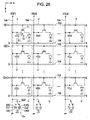
- Fig. 1 is a block diagram showing the configuration of an electro-optical device according to a first embodiment of the invention.
- Fig. 2 is a circuit diagram showing a detailed electrical configuration of each unit circuit.
- Fig. 3 is a diagram showing the operation for driving the electro-optical device.
- Fig. 4 is a diagram showing the operation in a write period.
- Fig. 5 is a circuit diagram showing the configuration of an electro-optical device according to a second embodiment of the invention.
- Fig. 6 is a circuit diagram showing the configuration of an electro-optical device according to a third embodiment of the invention.
- Fig. 7 is a circuit diagram showing the configuration of an electro-optical device according to a fourth embodiment of the invention.
- Fig. 8 is a diagram showing the operation timing of the electro-optical device according to the fourth embodiment.
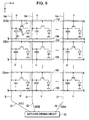
- Fig. 9 is a circuit diagram showing the configuration of a comparative example.
- Fig. 10 is a circuit diagram showing the configuration of an electro-optical device according to a fifth embodiment of the invention.
- Fig. 11 is a plan view of a unit circuit of an electro-optical device according to the first embodiment in a step of a manufacturing process.
- Fig. 12 is a plan view of the unit circuit of the electro-optical device according to the first embodiment in a step of the manufacturing process.
- Fig. 13 is a plan view of the unit circuit of the electro-optical device according to the first embodiment in a step of the manufacturing process.
- Fig. 14 is a plan view of the unit circuit of the electro-optical device according to the first embodiment in a step of the manufacturing process.
- Fig. 15 is a cross-section view taken along line XV - XV shown in Figs. 11 to 14 .
- Fig. 16 is a plan view of a unit circuit of an electro-optical device according to the first embodiment in a step of a manufacturing process.
- Fig. 17 is a plan view of the unit circuit of the electro-optical device according to the first embodiment in a step of the manufacturing process.
- Fig. 18 is a plan view of the unit circuit of the electro-optical device according to the first embodiment in a step of the manufacturing process.
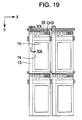
- Fig. 19 is a plan view of the unit circuit of the electro-optical device according to the first embodiment in a step of the manufacturing process.
- Fig. 20 is a cross section view taken along line XX - XX shown in Figs. 16 to 19 .
- Fig. 21 is a plan view of a unit circuit of an electro-optical device according to the second embodiment in a step of a manufacturing process.
- Fig. 22 is a plan view of the unit circuit of the electro-optical device according to the second embodiment in a step of the manufacturing process.
- Fig. 23 is a plan view of the unit circuit of the electro-optical device according to the second embodiment in a step of the manufacturing process.
- Fig. 24 is a plan view of the unit circuit of the electro-optical device according to the second embodiment in a step of the manufacturing process.
- Fig. 25 is a cross-section view taken along line XXV - XXV shown in Figs. 21 to 24 .
- Fig. 26 is a circuit diagram showing the configuration of an electro-optical device according to modified example 2 of the invention.
- Fig. 27 is a circuit diagram showing the configuration of an electro-optical device according to modified example 6 of the invention.
- Fig. 28 is a perspective view showing a detailed form of an electronic apparatus according to an embodiment of the invention.
- Fig. 29 is a perspective view showing a detailed form of an electronic apparatus according to an embodiment of the invention.
- Fig. 30 is a perspective view showing a detailed form of an electronic apparatus according to an embodiment of the invention.
- Fig. 31 is a circuit diagram showing the configuration of a general unit circuit.
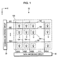
- Fig. 1 is a block diagram showing the configuration of an electro-optical device 10 according to a first embodiment of the invention.
- the electro-optical device 10 is a device that is employed in various electronic apparatuses as means for displaying an image.
- the electro-optical device has a pixel array unit 100 in which a plurality of unit circuits U are arranged in a planar shape, a scanning line driving circuit 20, and a data line driving circuit 30.
- the scanning line driving circuit 20 and the data line driving circuit 30 are shown as separate circuits, however, a part or the whole of the circuits may be configured as a single circuit.
- m scanning lines 102 that extend in the direction X and n data lines 104 that extend in the direction Y perpendicular to the direction X are disposed (here, m and n are natural numbers).
- Each unit circuit U is disposed in a position corresponding to an intersection of the scanning line 102 and the data line 104. Accordingly, the unit circuits U are arranged in the shape of a matrix of vertical m rows and horizontal n columns.
- the scanning line driving circuit 20 shown in Fig. 1 is a circuit for selecting the plurality of unit circuits U in units of rows.
- the scanning line driving circuit 20 generates scanning signals G[1] to G[m] that sequentially are in an active state and outputs the scanning signals to the m scanning lines 102.
- Transition to the active state of the scanning signal G[i] supplied to the scanning line 102 of the i-th row means selection of n unit circuits U belonging to the i-th row.
- the data line driving circuit 30 shown in Fig. 1 generates data electric potentials VD[1] to VD[n] corresponding to gray scale data of the n unit circuits U of one row corresponding to the scanning line 102 selected by the scanning line driving circuit 20 and outputs the data electric potentials to the data lines 104.
- the data electric potential VD output to the j-th (where j is an integer satisfying the condition of "1 ⁇ j ⁇ n") data line 104 is denoted by VD[j].
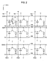
- Fig. 2 is a circuit diagram showing a detailed electrical configuration of each unit circuit U.
- each unit circuit U has an electro-optical element 12, a capacitor element C, and a transistor Tr.
- An electro-optical element 12 is an OLED element formed by interposing a light emitting layer formed of an organic EL material between an anode and a cathode.
- the electro-optical element 12 is disposed between the transistor Tr and a constant electric potential line (ground line) to which a constant electric potential is supplied.
- the anode is disposed in each unit circuit U and is a separate electrode that is controlled for each unit circuit U.
- the cathode is configured as a common electrode that is common to the unit circuits U.
- the cathode is connected to the constant electric potential line to which a constant electric potential is supplied.
- the capacitor element C shown in Fig. 2 is a unit for maintaining the data electric potential VD[j] supplied from the data line 104. As shown in Fig. 2 , the capacitor element C has a first electrode E1 connected to a capacitor line 106 and a second electrode E2 connected to the data line 104. The capacitor line 106 to which a constant electric potential is supplied is commonly connected to the unit circuits U.
- the ground electric potential may be configured that a negative electric potential is supplied to the constant electric potential line, the data electric potential VD[N], which represent the highest luminance, of the data electric potentials VD[j] is the constant electric potential, and the data electric potential VD[1], which represents the lowest luminance, of the data electric potentials VD[j] is a negative electric potential.
- the ground electric potential may be positioned between the data electric potential VD[N] and the data electric potential VD[1]. In such a case, the amplitude of the data electric potential VD[j] with respect to the ground electric potential can decrease, and accordingly, low power consumption can be achieved.
- the N-channel-type transistor Tr shown in Fig. 2 is a switching element that is in a conductive state at a time when the scanning line 102 is selected, so that the second electrode E2 of the capacitor element C and the electro-optical element 12 are in a conductive state.
- the source of the transistor Tr is connected to the anode of the electro-optical element 12, and the drain of the transistor is connected to the data line 104 and the second electrode E2 of the capacitor element C.
- the gate of the transistor Tr is connected to the scanning line 102.
- the scanning signal G[i] transits to an active state
- the transistor Tr is in the ON state, and thereby the second electrode E2 and the electro-optical element 12 are in a conductive state.
- the transistor Tr is in the OFF state, and accordingly, the second electrode E2 and the electro-optical element 12 are in a non-conductive state.
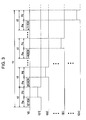
- each unit period 1T of one vertical scanning period 1V has a write period Pw that is a time period from a start time point of the unit period 1T to a time point when a predetermined time period elapses and a drive period Pd that is a time period after the write period Pw.
- the drive period Pd is set as a time period from an end time point of the write period Pw to an end time point of the unit period 1T.
- the scanning line driving circuit 20 shown in Fig. 1 sequentially selects one scanning line 102 at a time for each drive period Pd within one unit period 1T. For example, in the i-th unit period 1T within one vertical scanning period 1V, the scanning signal G[i] is set to have the active level, and accordingly, the scanning line 102 of the i-th row is selected.
- the data line driving circuit 30 shown in Fig. 1 outputs a data electric potential VD corresponding to the gray scale data of the electro-optical element 12 of each unit circuit U corresponding to the scanning line 102 that is selected by the scanning line driving circuit 20 in the drive period Pd within each unit period 1T to each data line 104 for the write period Pw within the each unit period 1T.
- data electric potentials VD[1] to VD[n] corresponding to gray scale data of n unit circuits U of the i-th row are output to the data lines 104.
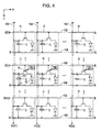
- the operation for driving the electro-optical element 12 will be described separately for the write period Pw and the drive period Pd with the unit circuits U of the i-th row focused.
- electric charges corresponding to the data electric potentials VD that are in correspondence with the gray scale data of the unit circuits U of the i-th row are charged (accumulated) in the capacitor elements C of the unit circuits U.
- electric charges corresponding to the data electric potential VD[j] that is in correspondence with the gray scale data of the j-th unit circuit U of the i-th row are charged in m capacitor elements C connected to the j-th data line 104 in a parallel manner.
- the electro-optical element 12 disposed in the j-th unit circuit U of the i-th row electric charges that are charged in the write period Pw are simultaneously supplied from m capacitor elements C connected to the j-th data line 104. Accordingly, the electro-optical elements 12 of the unit circuits U of the i-th row emit light at gray scale levels corresponding to the data electric potentials VD.
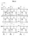
- Fig. 5 is a circuit diagram showing the configuration of an electro-optical device 10 according to a second embodiment of the invention.
- the constant electric potential line additionally serves as the capacitor line 106, which is different from the configuration of the first embodiment. Described in more details, as shown in Fig. 5 , to the constant electric potential line 108 that is commonly connected to the unit circuits U, the cathodes of the electro-optical elements 12 of the unit circuits U are commonly connected, and the first electrodes E1 of the capacitor elements C of the unit circuits U are commonly connected the constant electric potential line.
- the capacitor line 106 is not needed in addition to the constant electric potential line 108. Therefore, the configuration of the electro-optical device 10 can be simplified.
- Fig. 6 is a circuit diagram showing the configuration of an electro-optical device 10 according to a third embodiment of the invention.
- an auxiliary capacitor element Cs having one electrode connected to the data line 104 is disposed, which is different from the configuration of each of the above-described embodiments.
- Other configurations are the same as those of the above-described embodiments, and thus, descriptions of duplicate parts thereof are omitted here.
- one electrode E3 of the auxiliary capacitor element Cs is connected to the data line 104, and the other electrode E4 thereof is connected to the electric potential line to which a constant electric potential is supplied.
- the auxiliary capacitor element Cs is also charged.
- electric charges transferred from the auxiliary capacitor element Cs are supplied to the unit circuit U corresponding to the auxiliary capacitor element Cs.
- the electric potential line for example, may be the capacitor line 106 shown in Fig. 2 or the constant electric potential line 108 shown in Fig. 5 .
- the lacking amount can be supplemented by using the capacitance of the auxiliary capacitor element Cs connected to the data line 104.
- Fig. 7 is a circuit diagram showing the configuration of an electro-optical device 10 according to a fourth embodiment of the invention.
- each data line 104 is connected to m unit circuits U and is configured by a first part Z1 having a same length for each data line 104 and a second part Z2 connected to the data line driving circuit 30.
- the data line driving circuit 30 is disposed in the center of the pixel array unit 100 in direction X, and each data line 104 is bent so as to be connected to the data line driving circuit 30.
- the range of the pixel array unit 100 in which the data lines 104 are distributed in direction X is broader than the range in which the output terminals of the data lines 104 are distributed in the data line driving circuit 30, and accordingly, lengths of the data lines 104 are different from one another.
- the first parts Z1 of the data lines 104 have a same length, and thus, the lengths of the second parts Z2 of the data lines 104 are different from one another.
- a switch Sw that is used for switching the first and second parts between a conductive state and a non-conductive state is disposed.
- the switches Sw are controlled to be in the ON state or the OFF state all together by a control circuit not shown in the figure.
- the other configurations are the same as those of each of the above-described embodiments.
- the switch Sw is in the ON state for each write period Pw of one unit period 1T and is in the OFF state for each drive period Pd of the unit period 1T. Described in more details, in the write period Pw, the switches Sw are in the ON state all together, and the data lines 104 and the data line driving circuit 30 are in the conductive state. Accordingly, electric charges corresponding to the data electric potentials VD output from the data line driving circuit 30 are supplied to the data lines 104. On the other hand, in the drive period Pd, the switches Sw are in the OFF state all together, and the data lines 104 and the data line driving circuit 30 are in the non-conductive state. Accordingly, supply of the electric charges corresponding to the data electric potentials VD to the data lines 104 from the data line driving circuit 30 is stopped.
- Fig. 9 is a circuit diagram showing the configuration (hereinafter, referred to as a comparative example) in which the switch Sw is not disposed in each data line 104 and the first part Z1 and the second part Z2 are connected continuously.
- a comparative example parasitic capacitance not shown in the figure is included.
- the lengths of the second parts Z2 of the data lines 104 are different from one another.
- values of the parasitic capacitance of the data lines 104 are unbalanced. Accordingly, there is a problem that the amounts of light emission of the electro-optical elements 12 disperse for the data lines 104.
- the second parts Z2 having different lengths for the data lines 104 are separated from the data lines 104 in the drive period Pd.
- the lengths of the first parts Z1 of the data lines 104 are the same.
- the electric charges supplied to the electro-optical elements 12 of the unit circuits U of the row are uniform.
- Fig. 10 is a circuit diagram showing the configuration of an electro-optical device 10 according to a fifth embodiment of the invention.
- the capacitor element C is not disposed in each unit circuit U, which is different from the above-described embodiments.
- each unit circuit U has an electro-optical element 12 and a transistor Tr.
- the transistor Tr is disposed between a data line 104 and the electro-optical element 12 and is a unit that is in a conductive state at a time when a scanning line 102 is selected for making the data line and the electro-optical element to be in a conductive state.
- each of n data lines has a first part Z1 to which m unit circuits U are connected, a second part Z2 that is connected to a data line driving circuit 30, and a switch Sw that is interposed between the first part Z1 and the second part Z2.
- Each switch Sw is in a conductive state for each write period Pw so as to make the first part Z1 and the second part Z2 to be in a conductive state.
- each switch Sw is in a non-conductive state for each drive period Pd so as to make the first part Z1 and the second part Z2 to be in a non-conductive state.
- the switches Sw as in the fourth embodiment, are controlled to be in the ON state or the OFF state all together by a control circuit not shown in the figure.
- the operation of the electro-optical device 10 according to this embodiment is the same as that according to the fourth embodiment.
- the switches Sw are in the ON state all together. Accordingly, the data lines 104 and the data line driving circuit 30 are in the conductive state, and thereby data electric potentials VD[1] to VD[n] output from the data line driving circuit 30 are supplied to the data lines 104.
- the data electric potentials VD[1] to VD[n] corresponding to each gray scale data of the n unit circuits U that are selected in the drive period Pd of the i-th unit period 1T are supplied to the data lines 104. Accordingly, electric charges corresponding to the data electric potentials VD[1] to VD[n] are charged in capacitance (parasitic capacitance) that is accompanied in each data line 104.
- the length of the first part Z1 of each data line 104 is sufficiently larger than that of the second part Z2, and thus the value of parasitic capacitance generated between the first part Z1 and other elements (the scanning lien 102, the power supply line, and neighbor data lines 104, and the like) is sufficiently larger that generated between the second part Z2 and other elements. Accordingly, in the write period Pw of each unit period 1T, most of the electric charges according to the data electric potentials VD[1] to VD[n] output from the data line driving circuit 30 are charged in the capacitance accompanied in the first part Z1 of the data lines 104.
- the switches Sw are in the OFF state all together. Accordingly, the first part Z1 of each data line 104 is electrically separated from the data line driving circuit 30, and supply of the data electric potentials VD[1] to VD[n] from the data line driving circuit 30 to the data lines 104 is stopped.
- one scanning line 102 is selected by the scanning line driving circuit 20. To the electro-optical elements 12 of the unit circuits U corresponding to the selected scanning line 102, the electric charges charged in the write period Pw are supplied from the capacitance accompanied by the first parts Z1 of the data lines 104 corresponding to the unit circuits U.
- the electric charges charged in the capacitance accompanied in one data line 104 can be used for light emission of one electro-optical element 12. Accordingly, differently from the above-described embodiments, the capacitor element is not needed to be disposed in each unit circuit U. As a result, according to this embodiment, there is an advantage that high precision can be achieved, compared to a case where the configuration in which the capacitor element is disposed in each unit circuit U is used.
- the lengths of the first parts Z1 of the data lines 104 may be configured to be the same.
- the values of capacitance accompanied by the first parts Z1 of the data lines 104 can be uniform, and electric charges supplied to the electro-optical elements 12 of the unit circuits U of a row are uniform in a case where gray scale data of the unit circuits U of the row selected in the drive period Pd is the same.
- Figs. 11 to 14 are plan views showing appearances of each step in which the unit circuit U of the electro-optical device 10 according to the first embodiment is formed.
- Figs. 11 to 14 six unit circuits U in each stage are arranged in the direction X and the direction Y.
- Fig. 15 is a cross-section view taken along line XV - XV shown in Figs. 11 to 14 .
- Figs. 11 to 14 are plan views, for easy understanding of each element, to each element common to that shown in Fig. 15 , a same hatching pattern as that shown in Fig. 15 is appropriately used.
- a semiconductor layer 41 formed of a semiconductor material such as silicon is formed on the face of a substrate 40.
- the semiconductor layer 41 has a first part 41a and a second part 41b that extend in direction Y and a connection part 41c that extends in direction X and connects the first and second parts.
- the first part 41a serves as a drain region and also serves as a second electrode E2 of a capacitor element C of each unit circuit U.
- the second part 41b serves as a source region.
- the connection part 41c serves as a channel region.
- the entire surface of the substrate 40 on which the semiconductor layer 41 is formed is covered with a first insulating layer Fa1.
- a gate electrode 43 (scanning line 102) of the transistor Tr and a capacitor line 106 are formed on the face of the first insulating layer Fa1.
- the gate electrode 43 and the capacitor line 106 are formed together in a same process by patterning a conductive film (for example, a thin film made of aluminum) that is continuously formed over the entire area of the first insulating layer Fa1.
- the gate electrode 43 extends in direction X and is overlapped with the connection part 41c (gate region) of the semiconductor layer 41 through the first insulating layer Fa1 (not shown in Fig. 12 ).
- the capacitor line 106 serves as the first electrode E1 of the capacitor element C of each unit circuit U. As shown in Fig. 12 , the capacitor line 106 extends in direction X and is overlapped with the first part 41a of the semiconductor layer 41 through the first insulating layer Fa1 (not shown in Fig. 12 ). As shown in Fig. 15 , the capacitor line 106 (the first electrode E1) and the first part 41a (the second electrode E2) of the semiconductor layer 41 face each other with the first insulating layer Fa1 interposed therebetween, and thereby a capacitor C1 is formed.
- forming a plurality of elements by selectively removing a common film body (regardless of a single layer or a plurality of layers) in a same process will be represented only by "forming from a same layer", hereinafter.
- Elements formed from the same layer are naturally made of a same material, and film thicknesses thereof are approximately the same with one another.
- the entire surface of the first insulating layer Fa1 on which the gate electrode 43 and the capacitor line 106 are formed is covered with a second insulating layer Fa2.
- the data line 104 is formed on the face of the second insulating layer Fa2.
- the data line 104 is formed by patterning a conductive film (for example, a thin film made of aluminum) that is continuously formed over the entire area of the second insulating layer Fa2.
- the data line 104 extends in direction Y and is overlapped with the capacitor line 106 through the second insulating layer Fa2 (not shown in Fig. 13 ).
- the data line 104 and the capacitor line 106 face each other with the second insulating layer Fa2 interposed therebetween, and thereby a capacitor C2 is formed.
- the capacitor element C of each unit circuit U is formed by the capacitor C1 formed by bringing the first part 41a (the second electrode E2) of the semiconductor layer 41 and the capacitor line 106 (the first electrode E1) to face each other with the first insulating layer Fa1 interposed therebetween and the capacitor C2 formed by bringing the capacitor line 106 and the data line 104 to face each other with the second insulating layer Fa2 interposed therebetween.
- a plurality of capacitors that are formed in the direction of lamination in each unit circuit U forms the capacitor element C, and accordingly, the capacitance value of the capacitor element C in each unit circuit U can be sufficiently acquired.
- This configuration is particularly effective for a case where high definition of pixels is performed and the area of a planar part in each unit circuit U decreases.
- the data line 104 also serves as the drain electrode of the transistor Tr in each unit circuit U. As shown in Figs. 13 and 15 , the data line 104 and the first part 41a (the drain region) of the semiconductor layer 41 are in the conductive state through a contact hole CH.
- the source electrode 45 of the transistor Tr and the data line 104 are formed in a same layer, and the source electrode and the second part 41b (the source region) of the semiconductor layer 41 are in the conductive state through a contact hole CH2.
- the entire surface of the second insulating layer Fa2 on which the data line 104 is formed is covered with a third insulating layer Fa3.
- a third insulating layer Fa3 As shown in Figs. 14 and 15 , on the face of the third insulating layer Fa3, an anode 13 of the electro-optical element 12 is formed.
- the source electrode 45 of the transistor Tr and the anode 13 are in the conductive state through a contact hole CH3.
- various light-reflective conduction materials such as metal including aluminum, silver, or the like and alloy using the above-described material as a major component are used.
- a partition wall 14 used for dividing each unit circuit U is formed on the face of the third insulating layer Fa3 on which the anode 13 is formed.
- a light emitting layer 15 of the electro-optical element 12 is formed at least in a depression that is surrounded by the inner peripheral face of the partition wall 14 and has the anode 13 as its bottom.
- the light emitting element 15 may be formed on the partition wall 14.
- various function layers a hole injecting layer, a hole transport layer, an electron injecting layer, an electron transport layer, a hole blocking layer, and an electron blocking layer used for promoting or effectively performing the light emission of the light emitting layer 15 are laminated on the light emitting layer 15 may be used.
- a cathode 16 is formed so as to cover the light emitting layer 15 and the partition wall 14 of each unit circuit U.
- the cathode 16 is formed to be continuous over the electro-optical elements 12 of the unit circuits U.
- the cathode 16 is formed of a transparent conduction material such as ITO (Indium Tin Oxide) or IZO (Indium Zinc Oxide).
- the cathode 16 may be formed to include a material having a low work function such as alloy of Mg and Ag at a thickness for which light can be transmitted.
- light that is irradiated from the light emitting layer 15 to the cathode 16 side of the electro-optical element 12 and light that is irradiated to a side opposite to the cathode 16 from the light emitting layer 15, reflected from the anode 13, and forwarded toward the cathode 16 are transmitted through the cathode 16 to be output externally (top emission).
- the electro-optical device 10 may employ a bottom-emission-type structure.
- Figs. 16 to 19 are plan views showing appearances of each step in which each unit circuit U is formed in a case where the electro-optical device 10 is configured as the bottom-emission-type.
- Fig. 20 is a cross section view taken along line XX - XX shown in Figs. 16 to 19 .
- a semiconductor layer 51 is formed of a semiconductor material such as silicon.
- the semiconductor layer 51 has a first part 51a that extends in direction Y and a second part 51b that extends in direction X.
- the first part 51a serves as a drain region of the transistor Tr and also serves as a second electrode E2 of a capacitor element C.
- the second part 51b serves as a channel region and a source region.
- the entire surface of the substrate 50 on which the semiconductor layer 51 is formed is covered with a first insulating layer Fb1.
- a gate electrode 53 (scanning line 102) of a transistor Tr and a capacitor line 106 are formed on the face of the first insulating layer Fb1.
- the gate electrode 53 and the capacitor line 106 are formed in a same layer.
- the gate electrode 53 has a first part 53a that extends in direction X and a second part 53b that extends in direction Y.
- the first part 53a serves as a scanning line 102.
- the second part 53b is overlapped with the second part 51b (channel region) of the semiconductor layer 51 through the first insulating layer Fb1 (not shown in Fig. 17 ).
- the capacitor line 106 has a first part 106a that extends in direction X and a second part 106b that extends in direction Y.
- the second part 106b of the capacitor line 106 is overlapped with the first part 51a of the semiconductor layer 51 through the first insulating layer Fb1 (not shown in Fig. 17 ).
- the second part 106b (the first electrode E1) of the capacitor line 106 and the first part 51a (the second electrode E2) of the semiconductor layer 51 face each other with the first insulating layer Fb1 interposed therebetween, and thereby a capacitor C11 is formed.
- the entire surface of the first insulating layer Fb1 in which the gate electrode 53 and the capacitor line 106 are formed is covered with a second insulating layer Fb2.
- the data line 104 is formed on the face of the second insulating layer Fb2.
- the data line 104 extends in direction Y and is overlapped with the second part 106b of the capacitor line 106 through the second insulating layer Fb2 (not shown in Fig. 18 ).
- Fig. 18 the data line 104 extends in direction Y and is overlapped with the second part 106b of the capacitor line 106 through the second insulating layer Fb2 (not shown in Fig. 18 ).
- the data line 104 and the second part 106b of the capacitor line 106 face each other with the second insulating layer Fb2 interposed therebetween, and thereby a capacitor C22 is formed.
- the capacitor element C of each unit circuit U is formed by the capacitor C11 formed by bringing the first part 51a (the first electrode E1) of the semiconductor layer 51 and the second part 106b (the second electrode E2) of the capacitor line 106 to face each other with the first insulating layer Fb1 interposed therebetween and the capacitor C22 formed by bringing the second part 106b of the capacitor line 106 and the data line 104 to face each other with the second insulating layer Fb2 interposed therebetween.
- the data line 104 and the first part 51a (the drain region) of the semiconductor layer 51 are in the conductive state through a contact hole CH.
- the source electrode 55 of the transistor Tr and the data line 104 are formed in a same layer, and the source electrode and the second part 51b (the source region) of the semiconductor layer 51 are in the conductive state through a contact hole CH2.
- the entire surface of the second insulating layer Fb2 on which the data line 104 is formed is covered with a third insulating layer Fb3.
- a third insulating layer Fb3 As shown in Figs. 19 and 20 , on the face of the third insulating layer Fb3, an anode 13 of the electro-optical element 12 is formed.
- the source electrode 55 of the transistor Tr and the anode 13 are in the conductive state through a contact hole CH3.
- the anode 13 is formed of a transparent conduction material.
- a partition wall 14 is formed on the face of the third insulating layer Fb3 on which the anode 13 is formed.
- a light emitting layer 15 of the electro-optical element 12 is formed at least in a depression that is surrounded by the inner peripheral face of the partition wall 14 and has the anode 13 as its bottom.
- a cathode 16 is formed so as to cover the light emitting layer 15 and the partition wall 14 of each unit circuit U.
- the cathode 16 is formed of a light-reflective conduction material.
- the cathode 16 may be formed to include a material having light-reflectivity such as aluminum or silver and a material having a low work function such as magnesium or calcium.
- light that is irradiated from the light emitting layer 15 to the anode 13 side of the electro-optical element 12 and light that is irradiated to the cathode 16 side from the light emitting layer 15, reflected from the cathode 16, and forwarded toward the anode 13 are output through the anode 13 (bottom emission).
- Figs. 21 to 24 are plan views showing appearances of each step in which the unit circuit U of the electro-optical device 10 according to the second embodiment is formed.
- Figs. 21 to 24 four unit circuits U in each stage are arranged in the direction X and the direction Y.
- Fig. 25 is a cross-section view taken along line XXV - XXV shown in Figs. 21 to 24 .
- Figs. 21 to 24 are plan views, for easy understanding of each element, to each element common to that shown in Fig. 25 , a same hatching pattern as that shown in Fig. 25 is appropriately used.
- semiconductor layers 61 and 71 formed of a semiconductor material such as silicon is formed on the face of a substrate 60.
- a semiconductor layer 61 extends in direction X and serves as a channel region of the transistor Tr.
- the semiconductor layer 71 serves as a first electrode E1 of the capacitor element C.
- the entire surface of the substrate 60 on which the semiconductor layer 61 and the semiconductor layer 71 are formed is covered with a first insulating layer Fc1.
- a gate electrode 63 (the scanning line 102) of the transistor Tr and a wiring 80 formed of a conductive material are formed on the face of the first insulating layer Fc1.
- the gate electrode 63 and the wiring 80 are formed in a same layer.
- the gate electrode 63 has a first part 63a that extends in direction X and a second part 63b that extends in direction Y.
- the first part 63a of the gate electrode 63 serves as the scanning line 102.
- the second part 63b of the gate electrode 63 is overlapped with the semiconductor layer 61 (the channel region) through the first insulating layer Fc1 (not shown in Fig. 22 ).
- the wiring 80 has a first part 80a having a rectangular shape and second parts 80b that extend from the edges of the first part 80a to the positive and negative sides of direction Y.
- the first part 80a of the wiring 80 also serves as a second electrode E2 of the capacitor element C.
- the first part 80a of the wiring 80 is overlapped with the semiconductor layer 71 (the first electrode E1).
- the semiconductor layer 71 (the first electrode E1) and the first part 80a (the second electrode E2) of the wiring 80 face each other with the first insulating layer Fc1 interposed therebetween, and thereby a capacitor C111 is formed.
- the entire surface of the first insulating layer Fc1 in which the gate electrode 63 and the wiring 80 are formed is covered with a second insulating layer Fc2.
- the drain electrode 65, the source electrode 67, and the constant electric potential line 108 are formed on the face of the second insulating layer Fc2.
- the drain electrode 65, the source electrode 67, and the constant electric potential line 108 are formed in a same layer.
- the drain electrode 65 has a first part 65a that extends in direction Y and a second part 65b that extends in direction X. As shown in Fig. 23 , the first part 65a of the drain electrode 65 and the second part 80b of the wiring 80 are connected together (conductive to each other) through a contact hole CH so as to form the data line 104. In addition, as shown in Fig. 23 , the second part 65b of the drain electrode 65 and the semiconductor layer 61 (the drain region) are in the conductive state through a contact hole CH2.
- the source electrode 67 extends in direction X so as to be in the conductive state with the semiconductor layer 61 (the source region) through a contact hole CH3.
- the constant electric potential line 108 that is formed of metal having low resistance extends in direction X so as to be overlapped with the first part 80a of the wiring 80.
- the constant electric potential line 108 and the first part 80a of the wiring 80 face each other with the second insulating layer Fc2 interposed therebetween, and thereby a capacitor C222 is formed.
- the capacitor element C of each unit circuit U is formed by the capacitor C111 formed by bringing the semiconductor layer 71 (the first electrode E1) of the semiconductor layer 71 and the first part 80a (the second electrode E2) of the wiring 80 to face each other with the first insulating layer Fc1 interposed therebetween and the capacitor C222 formed by bringing the constant electric potential line 108 and the first part 80a of the wiring 80 to face each other with the second insulating layer Fc2 interposed therebetween.
- the constant electric potential line 108 is connected to the semiconductor layer 71 (the first electrode E1) through a contact hole CH4.
- the entire surface of the second insulating layer Fc2 on which the drain electrode 65, the source electrode 67, and the constant electric potential line 108 are formed is covered with a third insulating layer Fc3.
- the anode 13 of the electro-optical element 12 and an intermediate conductive layer 90 are formed on the face of the third insulating layer Fc3.
- the anode 13 and the intermediate conductive layer 90 are formed in a same layer.
- the source electrode 67 of the transistor Tr and the anode 13 are in the conductive state through a contact hole CH5.
- the anode 13 is formed of a light-reflective conduction material.
- the constant electric potential line 108 and the intermediate conductive layer 90 are in the conductive state through a contact hole CH6.
- a partition wall 14 is formed on the face of the third insulating layer Fc3 on which the anode 13 and the intermediate conductive layer 90 are formed.
- a light emitting layer 15 of the electro-optical element 12 is formed in the shape of a depression that is surrounded by the inner peripheral face of the partition wall 14 and has the anode 13 as its bottom.
- the cathode 16 is formed so as to cover the anode 13 (not shown in Fig. 25 ), the partition wall 14, and the intermediate conductive layer 90 of each unit circuit U.
- the cathode 16 is formed to be continuous over the electro-optical elements 12 of the unit circuits U.
- the cathode 16 is in a conductive state with the intermediate conductive layer 90 through a contact hole CH7.
- the constant electric potential line 108 not only serves as one electrode of the capacitor element C but also serves as an auxiliary electrode used for decreasing the resistance of the cathode 16.
- the cathode 16 is formed of a transparent conduction material such as ITO (Indium Tin Oxide) or IZO (Indium Zinc Oxide).
- ITO Indium Tin Oxide
- IZO Indium Zinc Oxide
- light that is irradiated from the light emitting layer 15 to the cathode 16 side of the electro-optical element 12 and light that is irradiated to a side opposite to the cathode 16 from the light emitting layer 15, reflected from the anode 13, and forwarded toward the cathode 16 are transmitted through the cathode 16 to be output externally (top emission).
- the invention is not limited thereto, and a bottom-emission-type structure may be employed.
- the cathode 16 is formed of a high-resistance material such as ITO.
- the resistance of the cathode 16 can decrease by making the constant electric potential line 108 formed of a metal material having resistance lower than that of the cathode 16 and the cathode 16 to be in the contact state through contact holes CH6 and CH7. Accordingly, a voltage drop in the cathode 16 is suppressed.
- the static electric potential line 108 not only serves as the capacitor line 106 but also serves as an auxiliary wiring.
- the invention is not limited thereto, and, for example, a configuration in which the write period Pw starts after a predetermined time elapses from the start time point of the unit period 1T may be used.
- a case where the end time point of the write period Pw of each unit time 1T and the start time point of the drive time Pd are the same is exemplified.
- the invention is not limited thereto, and, for example, a configuration in which the drive time Pd starts before the write time Pw ends may be used.
- auxiliary capacitor element Cs having one electrode connected to the data line 104 is disposed in addition to the capacitor element C of each unit circuit U.
- auxiliary capacitor element Cs includes a plurality of capacitor elements having different capacitance values and a switching element that makes one capacitor element among the plurality of capacitor elements and the data line 104 in the conductive state is disposed between one electrode of each of the plurality of capacitor elements and the data line 104 may be used.
- Fig. 26 is a circuit diagram showing the configuration of an electro-optical device 10 according to modified example 2.
- the auxiliary capacitor element Cs is configured by a first capacitor element Cs1 and a second capacitor element Cs2 having different capacitance values (for example, the capacitance of Cs1 > the capacitance of Cs2).
- a switch Sw2 that makes one capacitor element between the first capacitor element Cs1 and the second capacitor element Cs2 and the data line 104 is disposed.
- the other electrode E40 of the first capacitance Cs1 and the other electrode E400 of the second capacitor element Cs2 are connected commonly to a constant power supply line to which a constant electric potential is supplied.
- the constant electric potential line for example, may be the capacitor line 106 shown in Fig. 2 or the constant electric potential line 108 shown in Fig. 5 .
- the switch Sw2 is controlled by a control circuit not shown in the figure.
- the write period Pw of each unit period 1T one between the first capacitor element Cs1 and the second capacitor element Cs2 is selected by the switch Sw2 to be conductive to the data line 104, and the selected capacitor element is charged.
- the drive period Pd of each unit period 1T electric charges from the capacitor element is supplied to a corresponding unit circuit U.
- an emission time of the electro-optical element 12 can be controlled. Accordingly, the amount of light emission of the electro-optical element 12 can be controlled at a plurality of levels.
- the auxiliary capacitor element Cs is configured by the first capacitor element Cs1 and the second capacitor element Cs2 in the configuration shown in Fig. 26 .
- the invention is not limited thereto, and the auxiliary capacitor element Cs is needed to include a plurality of capacitor elements having different capacitance values.
- the auxiliary capacitor element Cs may be configured by three capacitor elements having three different capacitance values. As the number of the capacitor elements having different capacitance values increases, there is an advantage that the capacitance value can be more delicately controlled.
- the transistor Tr of each unit circuit U is the N-channel type transistor.
- the invention is not limited thereto, and the transistor may be configured by a P-channel type transistor.
- the transistor Tr is configured as a switching element to be conductive at a time when the scanning line 102 is selected for making the second electrode E2 of the capacitor element C and the electro-optical element 12 to be in the conductive state.
- the switch Sw used for switching between conduction and non-conduction of the first and second parts is disposed between the first part Z1 and the second part Z2.
- the switch Sw may be configured by a thin film transistor, an N-channel type transistor, or a P-channel type transistor.
- an OLED has been described.
- an organic light emitting diode or an LED Light Emitting Diode
- an element of any type may be used as the electro-optical element as long as the element emits light at a light-emission luminance level corresponding to an electrical energy level.
- a configuration in which electric charges corresponding to the data electric potential VD are charged in the capacitance (parasitic capacitance) accompanied in the data line 104 has been exemplified.
- a configuration in which a capacitor element Cx used for charging electric charges in correspondence with the data electric potential VD is disposed in each data line 104 (the first part Z1) may be used. Even in such a case, as in the fifth embodiment, the capacitor element is not needed to be disposed in each unit circuit U. Accordingly, there is an advantage that high definition can be achieved.
- the number of the capacitor elements Cx disposed in each data line 104 may be one, or two or more.
- the position of the capacitor element Cx disposed in each data line 104 can be arbitrarily set.
- Fig. 28 is a perspective view showing the configuration of a mobile personal computer that uses the electro-optical device 10 according to any one of the above-described embodiments as a display unit.
- the personal computer 2000 includes a light emitting unit 10 as the display unit and a main body 2010. In the main body 2010, a power switch 2001 and a keyboard 2002 are disposed. Since the electro-optical device 10 uses the OLED element as the electro-optical element 12, a screen that has a wide viewing angle and can be easily viewed can be displayed.
- Fig. 29 shows the configuration of a cellular phone to which the electro-optical device 10 according to an embodiment of the invention is used.
- the cellular phone 3000 includes a plurality of operation buttons 3001, a scroll button 3002 and an electro-optical device 10 as a display unit. By operating the scroll button 3002, a screen displayed in the electro-optical device 10 is scrolled.
- Fig. 30 shows the configuration of a personal digital assistant (PDA) to which the electro-optical device 10 according to an embodiment of the invention is used.
- the personal digital assistant 4000 includes a plurality of operation buttons 4001, a power switch 4002, and the electro-optical device 10 as a display unit. By operating the power switch 4002, various types of information such as an address book or a schedule planner are displayed in the electro-optical device 10.
- an electro-optical device in addition to the electronic apparatuses shown in Figs. 28 to 30 , there are a digital camera, a television set, a video camera, a car navigation system, a pager, an electronic organizer, an electronic paper sheet, a calculator, a word processor, a workstation, a video phone, a POS terminal, a printer, a scanner, a copier, a video player, an apparatus having a touch panel, and the like.
- the use of the electro-optical device according to an embodiment of the invention is not limited to display of an image.
- an image forming device such as an optical write-type printer or an electronic copier
- a write head that exposes a photosensitive body in accordance with an image to be formed in a writing material such as a paper sheet
- the electro-optical device according to an embodiment of the invention can be also used for the write head of such type.
- An electronic circuit described in the embodiments of the invention includes a circuit that becomes a unit for exposure in an image forming device, in addition to a pixel circuit constituting pixels of the display device as in the above-described embodiments.
Abstract
Description
- The present invention relates to an electro-optical device using an electro-optical element, a method of driving the electro-optical device, and an electronic apparatus.
- Recently, various image display devices using electro-optical elements such as organic light emitting diode elements (hereinafter referred to as OLED) referred to as organic EL (Electroluminescent) elements, light emitting polymer elements, or the like have been proposed.
-
Fig. 31 is a diagram showing the configuration of a unit circuit P of an image display device disclosed inJP-A-2000-122608 JP-A-2000-122608 Fig. 31 shows the configuration of one unit circuit P of the plurality of the unit circuits. As shown inFig. 31 , the drain of an N-channel type transistor Ts is connected to the data line, and the source of the transistor is connected to an anode of an OLED element and one electrode of a capacitor element Co. The gate of the transistor Ts is connected to the scanning line. In addition, as shown inFig. 29 , the OLED element and the capacitor element Co are connected in parallel, and a cathode of the OLED element and the other electrode of the capacitor element Co is commonly connected to a fixed electric potential. - Under the above-described configuration, first, when a scanning signal supplied to the scanning line transits to an active state, the transistor Ts is in the ON state. Accordingly, a data electric potential supplied to the data line is supplied to the OLED element through the transistor Ts and is written in the capacitor element Co. Second, when the scanning signal transits to a non-active state, the transistor Ts is in the OFF state. However, while electric charges accumulated in the capacitor element Co remain, the light emitting state of the OLED element continues.
- However, in the configuration of
JP-A-2000-122608 - An advantage of some aspects of the invention is that it provides an electro-optical device using an electro-optical element, a method of driving the electro-optical device, and an electronic apparatus capable of acquiring a sufficient amount of light emission with the capacitance of the capacitor element of each unit circuit decreased.
- According to a first aspect of the invention, there is provided an electro-optical device including: a plurality of unit circuits that are disposed in correspondence with intersections of a plurality of scanning lines and a plurality of data lines; a scanning line driving circuit that sequentially selects one of the plurality of scanning lines for a drive period of each unit period; and a data line driving circuit that outputs data electric potentials corresponding to gray scale data of the plurality of unit circuits that are in correspondence with the one of the plurality of scanning lines selected for the each drive period of the each unit period to the plurality of data lines for each write period that is a period within the each unit period before the each drive period starts. Each of the plurality of unit circuits has: an electro-optical element that has a gray scale level corresponding to the data electric potential; a capacitor element that has a first electrode connected to a capacitor line and a second electrode connected to the data line; and a switching element that is disposed between the second electrode and the electro-optical element and is in a conductive state at a time when the one of the plurality of scanning line is selected by the scanning line driving circuit for making the second electrode and the electro-optical element to be conductive to each other. In the above-described electro-optical device, it may be configured that, for the each write period, electric charges corresponding to the data electric potential that is output from the data line driving circuit are charged in the capacitor element of the each unit circuit and, for the each drive period, the electric charges charged in the write period are supplied to the electro-optical element of the each unit circuit corresponding to the one of the plurality of scanning lines selected by the scanning line driving circuit from a plurality of the capacitor elements connected to the data line corresponding to the each unit circuit.
- According to the above-described electro-optical device, for the drive period of each unit period, electric charges charged for the write period within the unit period are supplied altogether to the unit circuit corresponding to the scanning line selected by the scanning line driving circuit from the plurality of capacitor elements connected to the data line corresponding to the unit circuit.
Accordingly, the light emitting time of the electro-optical element of the unit circuit can be acquired sufficiently. As a result, the amount of light emission of the electro-optical element can be a sufficient value, and the required capacitance value of the capacitor element of each unit circuit can decrease, compared to that in a configuration (hereinafter, referred to as a general example) shown inFig. 31 . - In the above-described electro-optical device, the electro-optical element of each of the plurality of unit circuits may include a third electrode connected to the switching element, a fourth electrode connected to a constant electric potential line to which a constant electric potential is supplied, and an optical layer that is interposed between the third electrode and the fourth electrode, and the capacitor line may be the constant electric potential line. In such a case, the capacitor line is not needed separately from the electric potential line, and accordingly, the configuration of the electro-optical device can be simplified.
- In the above-described electro-optical device, an auxiliary capacitor element having one electrode connected to the data line may be disposed in each of the unit circuits in addition to the capacitor element of each of the unit circuits. In such a case, even when the total capacitance value of the capacitor elements connected to the data line corresponding to the unit circuit is smaller than the capacitance value needed for a sufficient value of the amount of light emission of the electro-optical device of the unit circuit corresponding to the selected scanning line, the lacking amount can be supplemented by the capacitance of the auxiliary capacitor.
- The above-described electro-optical device may further include switching elements that connect the data line driving circuit and the plurality of data lines, as an appropriate embodiment of the invention. In addition, it may be configured that the auxiliary capacitor element includes a plurality of capacitor elements having different capacitance values and a second switching element that makes one capacitor element of the plurality of the capacitor elements to be conductive to the data line is disposed between the electrodes of the plurality of the capacitor elements and the data line, as a more appropriate embodiment of the invention. In such a case, the light emitting time of the electro-optical element can be controlled by selectively making any one of the plurality of capacitor elements to be conductive to the data line in the write period. Accordingly, the amount of light emission of the electro-optical element can be controlled to be at a plurality of levels.
- In the above-described electro-optical device, it may be configured that each of the plurality of the data lines is configured by a first part that is connected to the plurality of the unit circuits and has a same length in the plurality of the data lines and a second part that is connected to the data line driving circuit and has a different length in the plurality of the data lines, a third switching element used for switching between conduction and non-conduction of the first part and the second part is disposed between the first part and the second part, and the third switching element is in the ON state for each of the write period of the each unit period and is in the OFF state for each of the drive period of the each unit period. In such a case, the second part of each data line is separated in the drive period of each unit period. Since the lengths of the first parts of the data lines are the same, occurrence of unbalance of capacitor values in the data lines can be suppressed. Accordingly, dispersion of the amounts of light emission of the electro-optical elements for each data line can be suppressed.
- According to a second aspect of the invention, there is provided an electro-optical device including: a plurality of scanning lines; a plurality of data lines; a plurality of unit circuits that are disposed in correspondence with the plurality of scanning lines and the plurality of data lines; and a plurality of capacitor elements that are disposed along the plurality of data lines. Each of the plurality of unit circuits has: an electro-optical element; and a switching element that is controlled in accordance with a scanning signal supplied to one scanning line of the plurality of scanning lines and controls conduction between the plurality of capacitor elements and the electro-optical element.
- In the above-described electro-optical device, it may be configured that the plurality of unit circuits has a unit circuit group formed of two or more unit circuits connected to one data line of the plurality of data lines, and the plurality of capacitor elements is separately disposed in correspondence with each of the unit circuits belonging to the unit circuit group.
- According to a third aspect of the invention, there is provided an electro-optical device including: a plurality of unit circuits that are disposed in correspondence with intersections of a plurality of scanning lines and a plurality of data lines; a scanning line driving circuit that sequentially selects one of the plurality of scanning lines for each drive period of each unit period; a data line driving circuit that outputs data electric potentials corresponding to gray scale data of the plurality of unit circuits that are in correspondence with the one of the plurality of scanning lines selected for the each drive period of the each unit period to the plurality of data lines for each write period that is a period within the each unit period before the each drive period starts; and a first switching element (for example, a switch Sw shown in
Fig. 10 ) that is a switching element disposed in correspondence with each of the plurality of data lines, is in a conductive state for the each write period so as to make the data line and the data line driving circuit to be conductive to each other, and is in a non-conductive state for the each drive period so as to make the data line and the data line driving circuit to be non-conductive to each other. Each of the plurality of unit circuits has: an electro-optical element that has a gray scale level corresponding to the data electric potential; and a second switching element (for example, a transistor Tr shown inFig. 10 ) that is disposed between the data line and the electro-optical element and is in the conductive state at a time when the scanning line is selected by the scanning line driving circuit so as to make the data line and the electro-optical element to be conductive to each other. In addition, for the write period, electric charges corresponding the data electric potential output from the data line driving circuit are charged in each data line (for example, first parts Z1 shown inFig. 10 ), and, for the drive period, the plurality of data lines is electrically separated from the data line driving circuit and the electric charges charged for the write period are supplied to the electro-optical element of each of the plurality of unit circuits corresponding to the scanning line selected by the scanning line driving circuit from the capacitance accompanied in the data line corresponding to the each of the plurality of unit circuits. - According to the above-described electro-optical device, the electric charges charged in the capacitance accompanied in one data line for the write period can be used for light emission of one electro-optical element for the drive period, and accordingly, the capacitor element is not needed to be disposed in each unit circuit. As a result, there is an advantage that high definition can be achieved, compared to a configuration in which the capacitor element is disposed in each unit circuit.
- The above-described electro-optical device may be used in various electronic apparatuses. A typical example of the electronic apparatus is an apparatus in which a light emitting device is used as a display unit. As apparatuses of this type, there are a personal computer, a cellular phone, and the like. However, the use of the light emitting device according to an embodiment of the invention is not limited to display of an image. For example, in an image forming apparatus (printing apparatus) having a configuration in which a latent image is formed in an image carrier such as photosensitive drum by projecting a light beam, the electro-optical device according to an embodiment of the invention may be used as an exposure unit (so-called an exposure head) that exposes the image carrier.
- According to a fourth aspect of the invention, there is provided a method of driving an electro-optical device including a plurality of unit circuits that are disposed in correspondence with intersections of a plurality of scanning lines and a plurality of data lines. Each of the plurality of unit circuits includes: an electro-optical element that has a gray scale level corresponding to a data electric potential; a capacitor element that has a first electrode connected to a capacitor line and a second electrode connected to the data line; and a switching element that is disposed between the second electrode and the electro-optical element and is in the conductive state at a time when the scanning line is selected so as to make the second electrode and the electro-optical element to be conductive to each other. The method includes: sequentially selecting one of the plurality of the scanning lines for each drive period of the each unit period; and outputting data electric potentials corresponding to gray scale data of the unit circuits that are in correspondence with the scanning line selected for the drive period of each unit period to the plurality of data lines for each write period that is a period within the each unit period before the drive period starts.
- According to a fifth aspect of the invention, there is provided a method of driving an electro-optical device including a plurality of unit circuits that are disposed in correspondence with intersections of a plurality of scanning lines and a plurality of data lines. Each of the plurality of unit circuits includes an electro-optical element that has a gray scale level corresponding to a data electric potential. The method includes: charging electric charges corresponding to the data electric potentials in capacitance accompanied in the data lines by outputting the data electric potentials corresponding to the gray scale data of the unit circuits that are in correspondence with the scanning line selected in a drive period of each unit period for each write period that is a period within the each unit circuit before the drive period starts; sequentially selecting one of the plurality of scanning lines for the drive period of the each unit period; and supplying the electric charges charged in the write period of the each unit period to the electro-optical element of the unit circuit from the capacitance accompanied in the data line corresponding to the unit circuit belonging to the selected scanning line.
- The invention will be described with reference to the accompanying drawings, wherein like numbers reference like elements.
-
Fig. 1 is a block diagram showing the configuration of an electro-optical device according to a first embodiment of the invention. -
Fig. 2 is a circuit diagram showing a detailed electrical configuration of each unit circuit. -
Fig. 3 is a diagram showing the operation for driving the electro-optical device. -
Fig. 4 is a diagram showing the operation in a write period. -
Fig. 5 is a circuit diagram showing the configuration of an electro-optical device according to a second embodiment of the invention. -
Fig. 6 is a circuit diagram showing the configuration of an electro-optical device according to a third embodiment of the invention. -
Fig. 7 is a circuit diagram showing the configuration of an electro-optical device according to a fourth embodiment of the invention. -
Fig. 8 is a diagram showing the operation timing of the electro-optical device according to the fourth embodiment. -
Fig. 9 is a circuit diagram showing the configuration of a comparative example. -
Fig. 10 is a circuit diagram showing the configuration of an electro-optical device according to a fifth embodiment of the invention. -
Fig. 11 is a plan view of a unit circuit of an electro-optical device according to the first embodiment in a step of a manufacturing process. -
Fig. 12 is a plan view of the unit circuit of the electro-optical device according to the first embodiment in a step of the manufacturing process. -
Fig. 13 is a plan view of the unit circuit of the electro-optical device according to the first embodiment in a step of the manufacturing process. -
Fig. 14 is a plan view of the unit circuit of the electro-optical device according to the first embodiment in a step of the manufacturing process. -
Fig. 15 is a cross-section view taken along line XV - XV shown inFigs. 11 to 14 . -
Fig. 16 is a plan view of a unit circuit of an electro-optical device according to the first embodiment in a step of a manufacturing process. -
Fig. 17 is a plan view of the unit circuit of the electro-optical device according to the first embodiment in a step of the manufacturing process. -
Fig. 18 is a plan view of the unit circuit of the electro-optical device according to the first embodiment in a step of the manufacturing process. -
Fig. 19 is a plan view of the unit circuit of the electro-optical device according to the first embodiment in a step of the manufacturing process. -
Fig. 20 is a cross section view taken along line XX - XX shown inFigs. 16 to 19 . -
Fig. 21 is a plan view of a unit circuit of an electro-optical device according to the second embodiment in a step of a manufacturing process. -
Fig. 22 is a plan view of the unit circuit of the electro-optical device according to the second embodiment in a step of the manufacturing process. -
Fig. 23 is a plan view of the unit circuit of the electro-optical device according to the second embodiment in a step of the manufacturing process. -
Fig. 24 is a plan view of the unit circuit of the electro-optical device according to the second embodiment in a step of the manufacturing process. -
Fig. 25 is a cross-section view taken along line XXV - XXV shown inFigs. 21 to 24 . -
Fig. 26 is a circuit diagram showing the configuration of an electro-optical device according to modified example 2 of the invention. -
Fig. 27 is a circuit diagram showing the configuration of an electro-optical device according to modified example 6 of the invention. -
Fig. 28 is a perspective view showing a detailed form of an electronic apparatus according to an embodiment of the invention. -
Fig. 29 is a perspective view showing a detailed form of an electronic apparatus according to an embodiment of the invention. -
Fig. 30 is a perspective view showing a detailed form of an electronic apparatus according to an embodiment of the invention. -
Fig. 31 is a circuit diagram showing the configuration of a general unit circuit. -
Fig. 1 is a block diagram showing the configuration of an electro-optical device 10 according to a first embodiment of the invention. The electro-optical device 10 is a device that is employed in various electronic apparatuses as means for displaying an image. The electro-optical device has apixel array unit 100 in which a plurality of unit circuits U are arranged in a planar shape, a scanningline driving circuit 20, and a dataline driving circuit 30. InFig. 1 , although the scanningline driving circuit 20 and the data line drivingcircuit 30 are shown as separate circuits, however, a part or the whole of the circuits may be configured as a single circuit. - As shown in
Fig. 1 , in thepixel array unit 100,m scanning lines 102 that extend in the direction X andn data lines 104 that extend in the direction Y perpendicular to the direction X are disposed (here, m and n are natural numbers). Each unit circuit U is disposed in a position corresponding to an intersection of thescanning line 102 and thedata line 104. Accordingly, the unit circuits U are arranged in the shape of a matrix of vertical m rows and horizontal n columns. - The scanning
line driving circuit 20 shown inFig. 1 is a circuit for selecting the plurality of unit circuits U in units of rows. The scanningline driving circuit 20 generates scanning signals G[1] to G[m] that sequentially are in an active state and outputs the scanning signals to the m scanning lines 102. Transition to the active state of the scanning signal G[i] supplied to thescanning line 102 of the i-th row (where, i is an integer satisfying the condition of "1 ≤ i ≤ m") means selection of n unit circuits U belonging to the i-th row. - The data line driving
circuit 30 shown inFig. 1 generates data electric potentials VD[1] to VD[n] corresponding to gray scale data of the n unit circuits U of one row corresponding to thescanning line 102 selected by the scanningline driving circuit 20 and outputs the data electric potentials to the data lines 104. Hereinafter, the data electric potential VD output to the j-th (where j is an integer satisfying the condition of "1 ≤ j ≤ n")data line 104 is denoted by VD[j]. -
Fig. 2 is a circuit diagram showing a detailed electrical configuration of each unit circuit U. As shown inFig. 2 , each unit circuit U has an electro-optical element 12, a capacitor element C, and a transistor Tr. An electro-optical element 12 is an OLED element formed by interposing a light emitting layer formed of an organic EL material between an anode and a cathode. As shown inFig. 2 , the electro-optical element 12 is disposed between the transistor Tr and a constant electric potential line (ground line) to which a constant electric potential is supplied. Here, the anode is disposed in each unit circuit U and is a separate electrode that is controlled for each unit circuit U. The cathode is configured as a common electrode that is common to the unit circuits U. In addition, the cathode is connected to the constant electric potential line to which a constant electric potential is supplied. Alternatively, it may be configured that the anode is a common electrode and the cathode is a separate electrode. - The capacitor element C shown in
Fig. 2 is a unit for maintaining the data electric potential VD[j] supplied from thedata line 104. As shown inFig. 2 , the capacitor element C has a first electrode E1 connected to acapacitor line 106 and a second electrode E2 connected to thedata line 104. Thecapacitor line 106 to which a constant electric potential is supplied is commonly connected to the unit circuits U. Instead of supplying the ground electric potential to the constant electric potential line, for example, it may be configured that a negative electric potential is supplied to the constant electric potential line, the data electric potential VD[N], which represent the highest luminance, of the data electric potentials VD[j] is the constant electric potential, and the data electric potential VD[1], which represents the lowest luminance, of the data electric potentials VD[j] is a negative electric potential. In other words, the ground electric potential may be positioned between the data electric potential VD[N] and the data electric potential VD[1]. In such a case, the amplitude of the data electric potential VD[j] with respect to the ground electric potential can decrease, and accordingly, low power consumption can be achieved. - The N-channel-type transistor Tr shown in
Fig. 2 is a switching element that is in a conductive state at a time when thescanning line 102 is selected, so that the second electrode E2 of the capacitor element C and the electro-optical element 12 are in a conductive state. As shown inFig. 2 , the source of the transistor Tr is connected to the anode of the electro-optical element 12, and the drain of the transistor is connected to thedata line 104 and the second electrode E2 of the capacitor element C. In addition, the gate of the transistor Tr is connected to thescanning line 102. When the scanning signal G[i] transits to an active state, the transistor Tr is in the ON state, and thereby the second electrode E2 and the electro-optical element 12 are in a conductive state. On the other hand, when the scanning signal G[i] transits to a non-active state, the transistor Tr is in the OFF state, and accordingly, the second electrode E2 and the electro-optical element 12 are in a non-conductive state. - Next, the operation of the electro-
optical device 10 will be described. As shown inFig. 3 , eachunit period 1T of onevertical scanning period 1V has a write period Pw that is a time period from a start time point of theunit period 1T to a time point when a predetermined time period elapses and a drive period Pd that is a time period after the write period Pw. In this embodiment, the drive period Pd is set as a time period from an end time point of the write period Pw to an end time point of theunit period 1T. - The scanning
line driving circuit 20 shown inFig. 1 sequentially selects onescanning line 102 at a time for each drive period Pd within oneunit period 1T. For example, in the i-th unit period 1T within onevertical scanning period 1V, the scanning signal G[i] is set to have the active level, and accordingly, thescanning line 102 of the i-th row is selected. - The data line driving
circuit 30 shown inFig. 1 outputs a data electric potential VD corresponding to the gray scale data of the electro-optical element 12 of each unit circuit U corresponding to thescanning line 102 that is selected by the scanningline driving circuit 20 in the drive period Pd within eachunit period 1T to eachdata line 104 for the write period Pw within the eachunit period 1T. For example, in the write period Pw within the i-th unit period 1T of onevertical scanning period 1V, data electric potentials VD[1] to VD[n] corresponding to gray scale data of n unit circuits U of the i-th row are output to the data lines 104. Hereinafter, the operation for driving the electro-optical element 12 will be described separately for the write period Pw and the drive period Pd with the unit circuits U of the i-th row focused. - In the write period Pw, electric charges corresponding to the data electric potentials VD that are in correspondence with the gray scale data of the unit circuits U of the i-th row are charged (accumulated) in the capacitor elements C of the unit circuits U. For example, electric charges corresponding to the data electric potential VD[j] that is in correspondence with the gray scale data of the j-th unit circuit U of the i-th row are charged in m capacitor elements C connected to the j-
th data line 104 in a parallel manner. - In the drive period Pd, output terminals of the data line driving
circuit 30 are set to be in the high-impedance state, and the scanning signal G[i] transits to the high level as shown inFig. 3 . Thus, as shown inFig. 4 , the transistors Tr of the unit circuits U of the i-th row are in the ON state. Accordingly, the electric charges charged in the write period Pw are supplied to each unit circuit U of the i-th row from the plurality of the capacitor elements C that are connected to thedata line 104 corresponding to the unit circuit U. For example, to the electro-optical element 12 disposed in the j-th unit circuit U of the i-th row, electric charges that are charged in the write period Pw are simultaneously supplied from m capacitor elements C connected to the j-th data line 104. Accordingly, the electro-optical elements 12 of the unit circuits U of the i-th row emit light at gray scale levels corresponding to the data electric potentials VD. - Under the configuration according to this embodiment, in the drive period Pd within each
unit period 1T, to each unit circuit U corresponding to thescanning line 102 selected by the scanningline driving circuit 20, electric charges charged in the write period Pw of theunit period 1T are simultaneously supplied from the capacitor elements C connected to thedata line 104 that is in correspondence with the unit circuit U. In other words, the electric charges charged in the m capacitor elements C in the parallel manner can be used for light emission of one electro-optical element 12, and accordingly, a time for light emission of the electro-optical element 12 can be sufficiently acquired. As a result, according to this embodiment, the amount of light emission of each electro-optical element 12 can be a sufficient value, and capacitance required for the capacitor element C of each unit circuit U can be lowered, compared to that of a general case. -
Fig. 5 is a circuit diagram showing the configuration of an electro-optical device 10 according to a second embodiment of the invention. In this embodiment, the constant electric potential line additionally serves as thecapacitor line 106, which is different from the configuration of the first embodiment. Described in more details, as shown inFig. 5 , to the constant electricpotential line 108 that is commonly connected to the unit circuits U, the cathodes of the electro-optical elements 12 of the unit circuits U are commonly connected, and the first electrodes E1 of the capacitor elements C of the unit circuits U are commonly connected the constant electric potential line. According to this configuration, thecapacitor line 106 is not needed in addition to the constant electricpotential line 108. Therefore, the configuration of the electro-optical device 10 can be simplified. -
Fig. 6 is a circuit diagram showing the configuration of an electro-optical device 10 according to a third embodiment of the invention. According to this embodiment, in addition to the capacitor element C of each unit circuit U, an auxiliary capacitor element Cs having one electrode connected to thedata line 104 is disposed, which is different from the configuration of each of the above-described embodiments. Other configurations are the same as those of the above-described embodiments, and thus, descriptions of duplicate parts thereof are omitted here. - As shown in
Fig. 6 , one electrode E3 of the auxiliary capacitor element Cs is connected to thedata line 104, and the other electrode E4 thereof is connected to the electric potential line to which a constant electric potential is supplied. According to this embodiment, in the write period Pw of eachunit period 1T, the auxiliary capacitor element Cs is also charged. In addition, in the drive period Pd of eachunit period 1T, electric charges transferred from the auxiliary capacitor element Cs are supplied to the unit circuit U corresponding to the auxiliary capacitor element Cs. Here, the electric potential line, for example, may be thecapacitor line 106 shown inFig. 2 or the constant electricpotential line 108 shown inFig. 5 . - According to this embodiment, even when the sum of capacitance of the m capacitor elements C that is connected to the
data line 104 corresponding to one electro-optical element 12 is insufficient for a sufficient amount of light emission of the electro-optical element 12, the lacking amount can be supplemented by using the capacitance of the auxiliary capacitor element Cs connected to thedata line 104. -
Fig. 7 is a circuit diagram showing the configuration of an electro-optical device 10 according to a fourth embodiment of the invention. As shown inFig. 7 , according to this embodiment, eachdata line 104 is connected to m unit circuits U and is configured by a first part Z1 having a same length for eachdata line 104 and a second part Z2 connected to the data line drivingcircuit 30. According to this embodiment, the dataline driving circuit 30 is disposed in the center of thepixel array unit 100 in direction X, and eachdata line 104 is bent so as to be connected to the data line drivingcircuit 30. The range of thepixel array unit 100 in which thedata lines 104 are distributed in direction X is broader than the range in which the output terminals of thedata lines 104 are distributed in the dataline driving circuit 30, and accordingly, lengths of thedata lines 104 are different from one another. The first parts Z1 of thedata lines 104 have a same length, and thus, the lengths of the second parts Z2 of thedata lines 104 are different from one another. - As shown in
Fig. 7 , between the first part Z1 and the second part Z2 of eachdata line 104, a switch Sw that is used for switching the first and second parts between a conductive state and a non-conductive state is disposed. The switches Sw are controlled to be in the ON state or the OFF state all together by a control circuit not shown in the figure. The other configurations are the same as those of each of the above-described embodiments. - As shown in
Fig. 8 , the switch Sw is in the ON state for each write period Pw of oneunit period 1T and is in the OFF state for each drive period Pd of theunit period 1T. Described in more details, in the write period Pw, the switches Sw are in the ON state all together, and thedata lines 104 and the data line drivingcircuit 30 are in the conductive state. Accordingly, electric charges corresponding to the data electric potentials VD output from the data line drivingcircuit 30 are supplied to the data lines 104. On the other hand, in the drive period Pd, the switches Sw are in the OFF state all together, and thedata lines 104 and the data line drivingcircuit 30 are in the non-conductive state. Accordingly, supply of the electric charges corresponding to the data electric potentials VD to thedata lines 104 from the data line drivingcircuit 30 is stopped. -
Fig. 9 is a circuit diagram showing the configuration (hereinafter, referred to as a comparative example) in which the switch Sw is not disposed in eachdata line 104 and the first part Z1 and the second part Z2 are connected continuously. Generally, in eachdata line 104, parasitic capacitance not shown in the figure is included. As described above, the lengths of the second parts Z2 of thedata lines 104 are different from one another. Thus, under the configuration of the comparative example, values of the parasitic capacitance of thedata lines 104 are unbalanced. Accordingly, there is a problem that the amounts of light emission of the electro-optical elements 12 disperse for the data lines 104. On the other hand, according to this embodiment, the second parts Z2 having different lengths for thedata lines 104 are separated from thedata lines 104 in the drive period Pd. The lengths of the first parts Z1 of thedata lines 104 are the same. Thus, for example, when the gray scale data of each unit circuit U of the row selected in the drive period Pd is the same, the electric charges supplied to the electro-optical elements 12 of the unit circuits U of the row are uniform. In other words, according to this embodiment, there is an advantage that dispersion of the amounts of light emission of the electro-optical elements 12 for thedata lines 104 can be suppressed. -
Fig. 10 is a circuit diagram showing the configuration of an electro-optical device 10 according to a fifth embodiment of the invention. In this embodiment, the capacitor element C is not disposed in each unit circuit U, which is different from the above-described embodiments. - As shown in
Fig. 10 , each unit circuit U has an electro-optical element 12 and a transistor Tr. The transistor Tr is disposed between adata line 104 and the electro-optical element 12 and is a unit that is in a conductive state at a time when ascanning line 102 is selected for making the data line and the electro-optical element to be in a conductive state. In addition, as shown inFig. 10 , each of n data lines has a first part Z1 to which m unit circuits U are connected, a second part Z2 that is connected to a dataline driving circuit 30, and a switch Sw that is interposed between the first part Z1 and the second part Z2. Each switch Sw is in a conductive state for each write period Pw so as to make the first part Z1 and the second part Z2 to be in a conductive state. On the other hand, each switch Sw is in a non-conductive state for each drive period Pd so as to make the first part Z1 and the second part Z2 to be in a non-conductive state. The switches Sw, as in the fourth embodiment, are controlled to be in the ON state or the OFF state all together by a control circuit not shown in the figure. - The operation of the electro-
optical device 10 according to this embodiment is the same as that according to the fourth embodiment. As shown inFig. 8 , in the write period Pw of eachunit period 1T, the switches Sw are in the ON state all together. Accordingly, thedata lines 104 and the data line drivingcircuit 30 are in the conductive state, and thereby data electric potentials VD[1] to VD[n] output from the data line drivingcircuit 30 are supplied to the data lines 104. For example, in the write period Pw of the i-th unit period 1T of onevertical scanning period 1V, the data electric potentials VD[1] to VD[n] corresponding to each gray scale data of the n unit circuits U that are selected in the drive period Pd of the i-th unit period 1T are supplied to the data lines 104. Accordingly, electric charges corresponding to the data electric potentials VD[1] to VD[n] are charged in capacitance (parasitic capacitance) that is accompanied in eachdata line 104. - Here, the length of the first part Z1 of each
data line 104 is sufficiently larger than that of the second part Z2, and thus the value of parasitic capacitance generated between the first part Z1 and other elements (thescanning lien 102, the power supply line, andneighbor data lines 104, and the like) is sufficiently larger that generated between the second part Z2 and other elements. Accordingly, in the write period Pw of eachunit period 1T, most of the electric charges according to the data electric potentials VD[1] to VD[n] output from the data line drivingcircuit 30 are charged in the capacitance accompanied in the first part Z1 of the data lines 104. - As shown in
Fig. 8 , in the drive period Pd, the switches Sw are in the OFF state all together. Accordingly, the first part Z1 of eachdata line 104 is electrically separated from the data line drivingcircuit 30, and supply of the data electric potentials VD[1] to VD[n] from the data line drivingcircuit 30 to thedata lines 104 is stopped. In addition, onescanning line 102 is selected by the scanningline driving circuit 20. To the electro-optical elements 12 of the unit circuits U corresponding to the selectedscanning line 102, the electric charges charged in the write period Pw are supplied from the capacitance accompanied by the first parts Z1 of thedata lines 104 corresponding to the unit circuits U. - Under the configuration of this embodiment, the electric charges charged in the capacitance accompanied in one
data line 104 can be used for light emission of one electro-optical element 12. Accordingly, differently from the above-described embodiments, the capacitor element is not needed to be disposed in each unit circuit U. As a result, according to this embodiment, there is an advantage that high precision can be achieved, compared to a case where the configuration in which the capacitor element is disposed in each unit circuit U is used. - In addition, in this embodiment, as in the above-described fourth embodiment, the lengths of the first parts Z1 of the
data lines 104 may be configured to be the same. Under such a configuration, the values of capacitance accompanied by the first parts Z1 of thedata lines 104 can be uniform, and electric charges supplied to the electro-optical elements 12 of the unit circuits U of a row are uniform in a case where gray scale data of the unit circuits U of the row selected in the drive period Pd is the same. In other words, there is an advantage that dispersion of the amounts of light emission of the electro-optical elements 12 for thedata lines 104 can be suppressed. - Next, a detailed structure of the unit circuit U of the above-described electro-
optical device 10 will be described with reference to the accompanying drawings. In the drawings described below, for the convenience of description, the size and ratios of each element are appropriately changed from those of an actual device. -
Figs. 11 to 14 are plan views showing appearances of each step in which the unit circuit U of the electro-optical device 10 according to the first embodiment is formed. In the plan views shown inFigs. 11 to 14 , six unit circuits U in each stage are arranged in the direction X and the direction Y.Fig. 15 is a cross-section view taken along line XV - XV shown inFigs. 11 to 14 . AlthoughFigs. 11 to 14 are plan views, for easy understanding of each element, to each element common to that shown inFig. 15 , a same hatching pattern as that shown inFig. 15 is appropriately used. - As shown in
Figs. 11 and15 , on the face of asubstrate 40, asemiconductor layer 41 formed of a semiconductor material such as silicon is formed. As shown inFig. 11 , thesemiconductor layer 41 has afirst part 41a and asecond part 41b that extend in direction Y and aconnection part 41c that extends in direction X and connects the first and second parts. Thefirst part 41a serves as a drain region and also serves as a second electrode E2 of a capacitor element C of each unit circuit U. Thesecond part 41b serves as a source region. In addition, theconnection part 41c serves as a channel region. As shown inFig. 15 , the entire surface of thesubstrate 40 on which thesemiconductor layer 41 is formed is covered with a first insulating layer Fa1. - As shown in
Figs. 12 and15 , on the face of the first insulating layer Fa1, a gate electrode 43 (scanning line 102) of the transistor Tr and acapacitor line 106 are formed. Thegate electrode 43 and thecapacitor line 106 are formed together in a same process by patterning a conductive film (for example, a thin film made of aluminum) that is continuously formed over the entire area of the first insulating layer Fa1. As shown inFig. 12 , thegate electrode 43 extends in direction X and is overlapped with theconnection part 41c (gate region) of thesemiconductor layer 41 through the first insulating layer Fa1 (not shown inFig. 12 ). - The
capacitor line 106 serves as the first electrode E1 of the capacitor element C of each unit circuit U. As shown inFig. 12 , thecapacitor line 106 extends in direction X and is overlapped with thefirst part 41a of thesemiconductor layer 41 through the first insulating layer Fa1 (not shown inFig. 12 ). As shown inFig. 15 , the capacitor line 106 (the first electrode E1) and thefirst part 41a (the second electrode E2) of thesemiconductor layer 41 face each other with the first insulating layer Fa1 interposed therebetween, and thereby a capacitor C1 is formed. - As relationship between the
gate electrode 43 and thecapacitor line 106, forming a plurality of elements by selectively removing a common film body (regardless of a single layer or a plurality of layers) in a same process will be represented only by "forming from a same layer", hereinafter. Elements formed from the same layer are naturally made of a same material, and film thicknesses thereof are approximately the same with one another. When a configuration in which a plurality of elements is formed from a same layer is used, compared to a configuration in which the elements are formed in different layers, there is an advantage that simplification of a manufacturing process and reduction of the manufacturing cost can be achieved. - As shown in
Fig. 15 , the entire surface of the first insulating layer Fa1 on which thegate electrode 43 and thecapacitor line 106 are formed is covered with a second insulating layer Fa2. As shown inFigs. 13 and15 , on the face of the second insulating layer Fa2, thedata line 104 is formed. Thedata line 104 is formed by patterning a conductive film (for example, a thin film made of aluminum) that is continuously formed over the entire area of the second insulating layer Fa2. As shown inFig. 13 , thedata line 104 extends in direction Y and is overlapped with thecapacitor line 106 through the second insulating layer Fa2 (not shown inFig. 13 ). - As shown in
Fig. 15 , thedata line 104 and thecapacitor line 106 face each other with the second insulating layer Fa2 interposed therebetween, and thereby a capacitor C2 is formed. As shown inFig. 15 , the capacitor element C of each unit circuit U is formed by the capacitor C1 formed by bringing thefirst part 41a (the second electrode E2) of thesemiconductor layer 41 and the capacitor line 106 (the first electrode E1) to face each other with the first insulating layer Fa1 interposed therebetween and the capacitor C2 formed by bringing thecapacitor line 106 and thedata line 104 to face each other with the second insulating layer Fa2 interposed therebetween. Under the configuration of this embodiment, a plurality of capacitors that are formed in the direction of lamination in each unit circuit U forms the capacitor element C, and accordingly, the capacitance value of the capacitor element C in each unit circuit U can be sufficiently acquired. This configuration is particularly effective for a case where high definition of pixels is performed and the area of a planar part in each unit circuit U decreases. - The
data line 104 also serves as the drain electrode of the transistor Tr in each unit circuit U. As shown inFigs. 13 and15 , thedata line 104 and thefirst part 41a (the drain region) of thesemiconductor layer 41 are in the conductive state through a contact hole CH. - In addition, as shown in
Fig. 13 , thesource electrode 45 of the transistor Tr and thedata line 104 are formed in a same layer, and the source electrode and thesecond part 41b (the source region) of thesemiconductor layer 41 are in the conductive state through a contact hole CH2. - As shown in
Fig. 15 , the entire surface of the second insulating layer Fa2 on which thedata line 104 is formed is covered with a third insulating layer Fa3. As shown inFigs. 14 and15 , on the face of the third insulating layer Fa3, ananode 13 of the electro-optical element 12 is formed. As show inFig. 14 , thesource electrode 45 of the transistor Tr and theanode 13 are in the conductive state through a contact hole CH3. As the material of theanode 13, various light-reflective conduction materials such as metal including aluminum, silver, or the like and alloy using the above-described material as a major component are used. - As shown in
Figs. 14 and15 , on the face of the third insulating layer Fa3 on which theanode 13 is formed, apartition wall 14 used for dividing each unit circuit U is formed. Alight emitting layer 15 of the electro-optical element 12 is formed at least in a depression that is surrounded by the inner peripheral face of thepartition wall 14 and has theanode 13 as its bottom. Thelight emitting element 15 may be formed on thepartition wall 14. In addition, a configuration in which various function layers (a hole injecting layer, a hole transport layer, an electron injecting layer, an electron transport layer, a hole blocking layer, and an electron blocking layer) used for promoting or effectively performing the light emission of thelight emitting layer 15 are laminated on thelight emitting layer 15 may be used. - As shown in
Fig. 15 , acathode 16 is formed so as to cover thelight emitting layer 15 and thepartition wall 14 of each unit circuit U. Thecathode 16 is formed to be continuous over the electro-optical elements 12 of the unit circuits U. Thecathode 16 is formed of a transparent conduction material such as ITO (Indium Tin Oxide) or IZO (Indium Zinc Oxide). In addition, thecathode 16 may be formed to include a material having a low work function such as alloy of Mg and Ag at a thickness for which light can be transmitted. According to this embodiment, light that is irradiated from thelight emitting layer 15 to thecathode 16 side of the electro-optical element 12 and light that is irradiated to a side opposite to thecathode 16 from thelight emitting layer 15, reflected from theanode 13, and forwarded toward thecathode 16 are transmitted through thecathode 16 to be output externally (top emission). - The electro-
optical device 10 according to the first embodiment may employ a bottom-emission-type structure.Figs. 16 to 19 are plan views showing appearances of each step in which each unit circuit U is formed in a case where the electro-optical device 10 is configured as the bottom-emission-type.Fig. 20 is a cross section view taken along line XX - XX shown inFigs. 16 to 19 . - As shown in
Figs. 16 and20 , on the face of asubstrate 50, asemiconductor layer 51 is formed of a semiconductor material such as silicon. As shown inFig. 16 , thesemiconductor layer 51 has afirst part 51a that extends in direction Y and asecond part 51b that extends in direction X. Thefirst part 51a serves as a drain region of the transistor Tr and also serves as a second electrode E2 of a capacitor element C. Thesecond part 51b serves as a channel region and a source region. As shown inFig. 20 , the entire surface of thesubstrate 50 on which thesemiconductor layer 51 is formed is covered with a first insulating layer Fb1. - As shown in
Figs. 17 and20 , on the face of the first insulating layer Fb1, a gate electrode 53 (scanning line 102) of a transistor Tr and acapacitor line 106 are formed. Thegate electrode 53 and thecapacitor line 106 are formed in a same layer. As shown inFig. 17 , thegate electrode 53 has afirst part 53a that extends in direction X and asecond part 53b that extends in direction Y. Thefirst part 53a serves as ascanning line 102. Thesecond part 53b is overlapped with thesecond part 51b (channel region) of thesemiconductor layer 51 through the first insulating layer Fb1 (not shown inFig. 17 ). - As show in
Fig. 17 , thecapacitor line 106 has afirst part 106a that extends in direction X and asecond part 106b that extends in direction Y. As show inFig. 17 , thesecond part 106b of thecapacitor line 106 is overlapped with thefirst part 51a of thesemiconductor layer 51 through the first insulating layer Fb1 (not shown inFig. 17 ). As shown inFig. 20 , thesecond part 106b (the first electrode E1) of thecapacitor line 106 and thefirst part 51a (the second electrode E2) of thesemiconductor layer 51 face each other with the first insulating layer Fb1 interposed therebetween, and thereby a capacitor C11 is formed. - As shown in
Fig. 20 , the entire surface of the first insulating layer Fb1 in which thegate electrode 53 and thecapacitor line 106 are formed is covered with a second insulating layer Fb2. As shown inFigs. 18 and20 , on the face of the second insulating layer Fb2, thedata line 104 is formed. As shown inFig. 18 , thedata line 104 extends in direction Y and is overlapped with thesecond part 106b of thecapacitor line 106 through the second insulating layer Fb2 (not shown inFig. 18 ). As shown inFig. 20 , thedata line 104 and thesecond part 106b of thecapacitor line 106 face each other with the second insulating layer Fb2 interposed therebetween, and thereby a capacitor C22 is formed. As shown inFig. 20 , the capacitor element C of each unit circuit U is formed by the capacitor C11 formed by bringing thefirst part 51a (the first electrode E1) of thesemiconductor layer 51 and thesecond part 106b (the second electrode E2) of thecapacitor line 106 to face each other with the first insulating layer Fb1 interposed therebetween and the capacitor C22 formed by bringing thesecond part 106b of thecapacitor line 106 and thedata line 104 to face each other with the second insulating layer Fb2 interposed therebetween. - As shown in
Figs. 18 and20 , thedata line 104 and thefirst part 51a (the drain region) of thesemiconductor layer 51 are in the conductive state through a contact hole CH. In addition, as shown inFig. 18 , thesource electrode 55 of the transistor Tr and thedata line 104 are formed in a same layer, and the source electrode and thesecond part 51b (the source region) of thesemiconductor layer 51 are in the conductive state through a contact hole CH2. - As shown in
Fig. 20 , the entire surface of the second insulating layer Fb2 on which thedata line 104 is formed is covered with a third insulating layer Fb3. As shown inFigs. 19 and20 , on the face of the third insulating layer Fb3, ananode 13 of the electro-optical element 12 is formed. As shown inFig. 19 , thesource electrode 55 of the transistor Tr and theanode 13 are in the conductive state through a contact hole CH3. Theanode 13 is formed of a transparent conduction material. - As shown in
Figs. 19 and20 , on the face of the third insulating layer Fb3 on which theanode 13 is formed, apartition wall 14 is formed. Alight emitting layer 15 of the electro-optical element 12 is formed at least in a depression that is surrounded by the inner peripheral face of thepartition wall 14 and has theanode 13 as its bottom. - As shown in
Fig. 20 , acathode 16 is formed so as to cover thelight emitting layer 15 and thepartition wall 14 of each unit circuit U. Thecathode 16 is formed of a light-reflective conduction material. Here, thecathode 16 may be formed to include a material having light-reflectivity such as aluminum or silver and a material having a low work function such as magnesium or calcium. According to this embodiment, light that is irradiated from thelight emitting layer 15 to theanode 13 side of the electro-optical element 12 and light that is irradiated to thecathode 16 side from thelight emitting layer 15, reflected from thecathode 16, and forwarded toward theanode 13 are output through the anode 13 (bottom emission). -
Figs. 21 to 24 are plan views showing appearances of each step in which the unit circuit U of the electro-optical device 10 according to the second embodiment is formed. In the plan views shown inFigs. 21 to 24 , four unit circuits U in each stage are arranged in the direction X and the direction Y.Fig. 25 is a cross-section view taken along line XXV - XXV shown inFigs. 21 to 24 . AlthoughFigs. 21 to 24 are plan views, for easy understanding of each element, to each element common to that shown inFig. 25 , a same hatching pattern as that shown inFig. 25 is appropriately used. - As shown in
Figs. 21 and25 , on the face of asubstrate 60, semiconductor layers 61 and 71 formed of a semiconductor material such as silicon is formed. Asemiconductor layer 61 extends in direction X and serves as a channel region of the transistor Tr. Thesemiconductor layer 71 serves as a first electrode E1 of the capacitor element C. As shown inFig. 25 , the entire surface of thesubstrate 60 on which thesemiconductor layer 61 and thesemiconductor layer 71 are formed is covered with a first insulating layer Fc1. - As shown in
Figs. 22 and25 , on the face of the first insulating layer Fc1, a gate electrode 63 (the scanning line 102) of the transistor Tr and a wiring 80 formed of a conductive material are formed. Thegate electrode 63 and the wiring 80 are formed in a same layer. As shown inFig. 22 , thegate electrode 63 has afirst part 63a that extends in direction X and asecond part 63b that extends in direction Y. Thefirst part 63a of thegate electrode 63 serves as thescanning line 102. As shown inFig. 22 , thesecond part 63b of thegate electrode 63 is overlapped with the semiconductor layer 61 (the channel region) through the first insulating layer Fc1 (not shown inFig. 22 ). - As shown in
Fig. 22 , the wiring 80 has afirst part 80a having a rectangular shape andsecond parts 80b that extend from the edges of thefirst part 80a to the positive and negative sides of direction Y. Thefirst part 80a of the wiring 80 also serves as a second electrode E2 of the capacitor element C. As shown inFig. 22 , thefirst part 80a of the wiring 80 is overlapped with the semiconductor layer 71 (the first electrode E1). As shown inFig. 25 , the semiconductor layer 71 (the first electrode E1) and thefirst part 80a (the second electrode E2) of the wiring 80 face each other with the first insulating layer Fc1 interposed therebetween, and thereby a capacitor C111 is formed. - As shown in
Figs. 23 and25 , the entire surface of the first insulating layer Fc1 in which thegate electrode 63 and the wiring 80 are formed is covered with a second insulating layer Fc2. As shown inFigs. 23 and25 , on the face of the second insulating layer Fc2, thedrain electrode 65, thesource electrode 67, and the constant electricpotential line 108 are formed. Thedrain electrode 65, thesource electrode 67, and the constant electricpotential line 108 are formed in a same layer. - As shown in
Fig. 23 , thedrain electrode 65 has afirst part 65a that extends in direction Y and asecond part 65b that extends in direction X. As shown inFig. 23 , thefirst part 65a of thedrain electrode 65 and thesecond part 80b of the wiring 80 are connected together (conductive to each other) through a contact hole CH so as to form thedata line 104. In addition, as shown inFig. 23 , thesecond part 65b of thedrain electrode 65 and the semiconductor layer 61 (the drain region) are in the conductive state through a contact hole CH2. - As shown in
Fig. 23 , thesource electrode 67 extends in direction X so as to be in the conductive state with the semiconductor layer 61 (the source region) through a contact hole CH3. - As shown in
Figs. 23 and25 , the constant electricpotential line 108 that is formed of metal having low resistance extends in direction X so as to be overlapped with thefirst part 80a of the wiring 80. As shown inFig. 25 , the constant electricpotential line 108 and thefirst part 80a of the wiring 80 face each other with the second insulating layer Fc2 interposed therebetween, and thereby a capacitor C222 is formed. As shown inFig. 25 , the capacitor element C of each unit circuit U is formed by the capacitor C111 formed by bringing the semiconductor layer 71 (the first electrode E1) of thesemiconductor layer 71 and thefirst part 80a (the second electrode E2) of the wiring 80 to face each other with the first insulating layer Fc1 interposed therebetween and the capacitor C222 formed by bringing the constant electricpotential line 108 and thefirst part 80a of the wiring 80 to face each other with the second insulating layer Fc2 interposed therebetween. In addition, as shown inFig. 23 , the constant electricpotential line 108 is connected to the semiconductor layer 71 (the first electrode E1) through a contact hole CH4. - As shown in
Figs. 24 and25 , the entire surface of the second insulating layer Fc2 on which thedrain electrode 65, thesource electrode 67, and the constant electricpotential line 108 are formed is covered with a third insulating layer Fc3. As shown inFigs. 24 and25 , on the face of the third insulating layer Fc3, theanode 13 of the electro-optical element 12 and an intermediateconductive layer 90 are formed. Theanode 13 and the intermediateconductive layer 90 are formed in a same layer. As shown inFig. 24 , thesource electrode 67 of the transistor Tr and theanode 13 are in the conductive state through a contact hole CH5. In this embodiment, theanode 13 is formed of a light-reflective conduction material. In addition, as shown inFigs. 24 and25 , the constant electricpotential line 108 and the intermediateconductive layer 90 are in the conductive state through a contact hole CH6. - As shown in
Figs. 24 and25 , on the face of the third insulating layer Fc3 on which theanode 13 and the intermediateconductive layer 90 are formed, apartition wall 14 is formed. Alight emitting layer 15 of the electro-optical element 12 is formed in the shape of a depression that is surrounded by the inner peripheral face of thepartition wall 14 and has theanode 13 as its bottom. - As shown in
Fig. 25 , thecathode 16 is formed so as to cover the anode 13 (not shown inFig. 25 ), thepartition wall 14, and the intermediateconductive layer 90 of each unit circuit U. Thecathode 16 is formed to be continuous over the electro-optical elements 12 of the unit circuits U. As shown inFigs. 24 and25 , thecathode 16 is in a conductive state with the intermediateconductive layer 90 through a contact hole CH7. - Thus, the constant electric
potential line 108 not only serves as one electrode of the capacitor element C but also serves as an auxiliary electrode used for decreasing the resistance of thecathode 16. - In this embodiment, the
cathode 16 is formed of a transparent conduction material such as ITO (Indium Tin Oxide) or IZO (Indium Zinc Oxide). According to this embodiment, light that is irradiated from thelight emitting layer 15 to thecathode 16 side of the electro-optical element 12 and light that is irradiated to a side opposite to thecathode 16 from thelight emitting layer 15, reflected from theanode 13, and forwarded toward thecathode 16 are transmitted through thecathode 16 to be output externally (top emission). However, the invention is not limited thereto, and a bottom-emission-type structure may be employed. - In this embodiment, the
cathode 16 is formed of a high-resistance material such as ITO. However, the resistance of thecathode 16 can decrease by making the constant electricpotential line 108 formed of a metal material having resistance lower than that of thecathode 16 and thecathode 16 to be in the contact state through contact holes CH6 and CH7. Accordingly, a voltage drop in thecathode 16 is suppressed. In other words, the static electricpotential line 108 not only serves as thecapacitor line 106 but also serves as an auxiliary wiring. - The present invention is not limited to the above-described embodiments. Thus, for example, modifications as below can be made therein. In addition, two or more modified examples of modified examples described below may be combined.
- In each of the above-described embodiments, for example, as show in
Fig. 3 , a case where the end time point of the drive period Pd and the end time point of theunit period 1T are the same has been described. However, the invention is not limited thereto, and, for example, a configuration in which the drive period Pd ends before the end time point of theunit period 1T may be used. In addition, inFig. 3 , a case where the start time point of eachunit period 1T and the start time point of the write period Pw of theunit period 1T are the same is exemplified. However, the invention is not limited thereto, and, for example, a configuration in which the write period Pw starts after a predetermined time elapses from the start time point of theunit period 1T may be used. In addition, inFig. 3 , a case where the end time point of the write period Pw of eachunit time 1T and the start time point of the drive time Pd are the same is exemplified. However, the invention is not limited thereto, and, for example, a configuration in which the drive time Pd starts before the write time Pw ends may be used. - In the above-described third embodiment, a configuration in which the auxiliary capacitor element Cs having one electrode connected to the
data line 104 is disposed in addition to the capacitor element C of each unit circuit U has been described. However, for example, a configuration, in which the auxiliary capacitor element Cs includes a plurality of capacitor elements having different capacitance values and a switching element that makes one capacitor element among the plurality of capacitor elements and thedata line 104 in the conductive state is disposed between one electrode of each of the plurality of capacitor elements and thedata line 104 may be used. -
Fig. 26 is a circuit diagram showing the configuration of an electro-optical device 10 according to modified example 2. As shown inFig. 26 , the auxiliary capacitor element Cs is configured by a first capacitor element Cs1 and a second capacitor element Cs2 having different capacitance values (for example, the capacitance of Cs1 > the capacitance of Cs2). As shown inFig. 26 , between one electrode E30 of the first capacitor element Cs1 and one electrode E300 of the second capacitor element Cs2 and thedata line 104, a switch Sw2 that makes one capacitor element between the first capacitor element Cs1 and the second capacitor element Cs2 and thedata line 104 is disposed. In addition, as shown inFig. 26 , the other electrode E40 of the first capacitance Cs1 and the other electrode E400 of the second capacitor element Cs2 are connected commonly to a constant power supply line to which a constant electric potential is supplied. The constant electric potential line, for example, may be thecapacitor line 106 shown inFig. 2 or the constant electricpotential line 108 shown inFig. 5 . - The switch Sw2 is controlled by a control circuit not shown in the figure. In the write period Pw of each
unit period 1T, one between the first capacitor element Cs1 and the second capacitor element Cs2 is selected by the switch Sw2 to be conductive to thedata line 104, and the selected capacitor element is charged. Then, in the drive period Pd of eachunit period 1T, electric charges from the capacitor element is supplied to a corresponding unit circuit U. Under the configuration shown inFig. 26 , by selectively making one of the plurality of capacitor elements to be conductive to thedata line 104 in the write period Pw, an emission time of the electro-optical element 12 can be controlled. Accordingly, the amount of light emission of the electro-optical element 12 can be controlled at a plurality of levels. - In the configuration shown in
Fig. 26 , a case where the auxiliary capacitor element Cs is configured by the first capacitor element Cs1 and the second capacitor element Cs2 has been exemplified. However, the invention is not limited thereto, and the auxiliary capacitor element Cs is needed to include a plurality of capacitor elements having different capacitance values. For example, the auxiliary capacitor element Cs may be configured by three capacitor elements having three different capacitance values. As the number of the capacitor elements having different capacitance values increases, there is an advantage that the capacitance value can be more delicately controlled. - In each of the above-described embodiments, the transistor Tr of each unit circuit U is the N-channel type transistor. However, the invention is not limited thereto, and the transistor may be configured by a P-channel type transistor. For example, the transistor Tr is configured as a switching element to be conductive at a time when the
scanning line 102 is selected for making the second electrode E2 of the capacitor element C and the electro-optical element 12 to be in the conductive state. - In the above-described fourth embodiment, in each
data line 104, the switch Sw used for switching between conduction and non-conduction of the first and second parts is disposed between the first part Z1 and the second part Z2. For example, the switch Sw may be configured by a thin film transistor, an N-channel type transistor, or a P-channel type transistor. - In each of the above-described embodiments, as one example of the electro-
optical element 12, an OLED has been described. However, as the electro-optical element, an organic light emitting diode or an LED (Light Emitting Diode) may be used. In other words, an element of any type may be used as the electro-optical element as long as the element emits light at a light-emission luminance level corresponding to an electrical energy level. - In the above-described fifth embodiment, a configuration in which electric charges corresponding to the data electric potential VD are charged in the capacitance (parasitic capacitance) accompanied in the
data line 104 has been exemplified. However, for example, as shown inFig. 27 , a configuration in which a capacitor element Cx used for charging electric charges in correspondence with the data electric potential VD is disposed in each data line 104 (the first part Z1) may be used. Even in such a case, as in the fifth embodiment, the capacitor element is not needed to be disposed in each unit circuit U. Accordingly, there is an advantage that high definition can be achieved. The number of the capacitor elements Cx disposed in eachdata line 104 may be one, or two or more. In addition, the position of the capacitor element Cx disposed in eachdata line 104 can be arbitrarily set. - Next, an electronic apparatus using the electro-
optical device 10 according to an embodiment of the invention will be described.Fig. 28 is a perspective view showing the configuration of a mobile personal computer that uses the electro-optical device 10 according to any one of the above-described embodiments as a display unit. Thepersonal computer 2000 includes alight emitting unit 10 as the display unit and amain body 2010. In themain body 2010, apower switch 2001 and akeyboard 2002 are disposed. Since the electro-optical device 10 uses the OLED element as the electro-optical element 12, a screen that has a wide viewing angle and can be easily viewed can be displayed. -
Fig. 29 shows the configuration of a cellular phone to which the electro-optical device 10 according to an embodiment of the invention is used. Thecellular phone 3000 includes a plurality ofoperation buttons 3001, ascroll button 3002 and an electro-optical device 10 as a display unit. By operating thescroll button 3002, a screen displayed in the electro-optical device 10 is scrolled. -
Fig. 30 shows the configuration of a personal digital assistant (PDA) to which the electro-optical device 10 according to an embodiment of the invention is used. The personaldigital assistant 4000 includes a plurality ofoperation buttons 4001, apower switch 4002, and the electro-optical device 10 as a display unit. By operating thepower switch 4002, various types of information such as an address book or a schedule planner are displayed in the electro-optical device 10. - In addition, as electronic apparatuses to which an electro-optical device according to an embodiment of the invention is applied, in addition to the electronic apparatuses shown in
Figs. 28 to 30 , there are a digital camera, a television set, a video camera, a car navigation system, a pager, an electronic organizer, an electronic paper sheet, a calculator, a word processor, a workstation, a video phone, a POS terminal, a printer, a scanner, a copier, a video player, an apparatus having a touch panel, and the like. The use of the electro-optical device according to an embodiment of the invention is not limited to display of an image. For example, in an image forming device such as an optical write-type printer or an electronic copier, a write head that exposes a photosensitive body in accordance with an image to be formed in a writing material such as a paper sheet is used. The electro-optical device according to an embodiment of the invention can be also used for the write head of such type. An electronic circuit described in the embodiments of the invention includes a circuit that becomes a unit for exposure in an image forming device, in addition to a pixel circuit constituting pixels of the display device as in the above-described embodiments.
Claims (13)
- An electro-optical device comprising:a plurality of unit circuits that are disposed in correspondence with intersections of a plurality of scanning lines and a plurality of data lines;a scanning line driving circuit that sequentially selects the plurality of scanning lines; one scanning line being selected for a drive period of one unit period; anda data line driving circuit that outputs data electric potentials to the plurality of data lines for each write period of the one unit period, the data electric potentials corresponding to gray scale data of the plurality of unit circuits that are in correspondence with one scanning line selected for the drive period of the one unit period and the write period being a period before the drive period starts,each of the plurality of unit circuits having:an electro-optical element that has a gray scale level corresponding to the data electric potential;a capacitor element that has a first electrode connected to a capacitor line and a second electrode connected to the data line; anda switching element that is disposed between the second electrode and the electro-optical element and is in a conductive state at a time when the one of scanning line is selected by the scanning line driving circuit for making the second electrode and the electro-optical element to be conductive to each other.
- The electro-optical device according to Claim 1,
for the write period, electric charges corresponding to the data electric potential that is output from the data line driving circuit are charged in the capacitor element of the each unit circuit, and
for the drive period, the electric charges charged in the write period are supplied to the electro-optical element of the each unit circuit corresponding to the one scanning line selected by the scanning line driving circuit from a plurality of the capacitor elements connected to the data line corresponding to the each unit circuit. - The electro-optical device according to Claim 1,
the electro-optical element of each of the plurality of unit circuits including a third electrode connected to the switching element, a fourth electrode connected to a constant electric potential line to which a constant electric potential is supplied, and an optical layer that is interposed between the third electrode and the fourth electrode, and
the capacitor line being the constant electric potential line. - The electro-optical device according to Claim 1, further comprising switching elements that connect the data line driving circuit and the plurality of data lines.
- The electro-optical device according to Claim 1,
an auxiliary capacitor element having one electrode connected to the data line being disposed in each of the unit circuits in addition to the capacitor element of each of the unit circuits. - The electro-optical device according to Claim 5,
the auxiliary capacitor element including a plurality of capacitor elements having different capacitance values, and
a second switching element that makes one capacitor element of the plurality of the capacitor elements to be conductive to the data line being disposed between the electrodes of the plurality of the capacitor elements and the data line. - The electro-optical device according to Claim 1,
each of the plurality of the data lines being configured by a first part that is connected to the plurality of the unit circuits and having a same length in the plurality of the data lines and a second part that is connected to the data line driving circuit and has a different length in the plurality of the data lines,
a third switching element used for switching between conduction and non-conduction of the first part and the second part being disposed between the first part and the second part, and
the third switching element being in an ON state for each of the write period of the unit period and is in an OFF state for each of the drive period of the unit period. - An electro-optical device comprising:a plurality of scanning lines;a plurality of data lines;a plurality of unit circuits that are disposed in correspondence with the plurality of scanning lines and the plurality of data lines; anda plurality of capacitor elements that are disposed along the plurality of data lines,each of the plurality of unit circuits having:an electro-optical element; anda switching element that is controlled in accordance with a scanning signal supplied to one scanning line of the plurality of scanning lines and controls conduction between the plurality of capacitor elements and the electro-optical element.
- An electro-optical device according to Claim 8,
the plurality of unit circuits having a unit circuit group formed of two or more unit circuits connected to one data line of the plurality of data lines, and
the plurality of capacitor elements being separately disposed in correspondence with each of the unit circuits belonging to the unit circuit group. - An electro-optical device comprising:a plurality of unit circuits that are disposed in correspondence with intersections of a plurality of scanning lines and a plurality of data lines;a scanning line driving circuit that sequentially selects the plurality of scanning lines, one scanning line being selected for each drive period of one unit period; anda data line driving circuit that outputs data electric potentials to the plurality of data lines for each write period of the one period unit, the data electric potentials corresponding to gray scale data of the plurality of unit circuits that are in correspondence with the one scanning line selected for the drive period of the one unit period and the write period being a period before the drive period starts; anda first switching element that is a switching element disposed in correspondence with each of the plurality of data lines, is in a conductive state for the write period so as to make the data line and the data line driving circuit to be conductive to each other, and is in a non-conductive state for the drive period so as to make the data line and the data line driving circuit to be non-conductive to each other,each of the plurality of unit circuits having:an electro-optical element that has a gray scale level corresponding to the data electric potential; anda second switching element that is disposed between the data line and the electro-optical element and is in the conductive state at a time when the scanning line is selected by the scanning line driving circuit so as to make the data line and the electro-optical element to be conductive to each other,for the write period, electric charges corresponding the data electric potential output from the data line driving circuit being charged in each data line, andfor the drive period, the plurality of data lines is electrically separated from the data line driving circuit and the electric charges charged for the write period being supplied to the electro-optical element of each of the plurality of unit circuits corresponding to the scanning line selected by the scanning line driving circuit from the capacitance accompanied in the data line corresponding to the each of the plurality of unit circuits.
- An electronic apparatus including the electro-optical device according to Claim 1.
- A method of driving an electro-optical device including a plurality of unit circuits that are disposed in correspondence with intersections of a plurality of scanning lines and a plurality of data lines,
each of the plurality of unit circuits including:an electro-optical element that has a gray scale level corresponding to a data electric potential;a capacitor element that has a first electrode connected to a capacitor line and a second electrode connected to the data line; anda switching element that is disposed between the second electrode and the electro-optical element and is in the conductive state at a time when one scanning line of the plurality of scanning lines is selected so as to make the second electrode and the electro-optical element to be conductive to each other,the method comprising:sequentially selecting the plurality of the scanning lines, the one scanning line being selected for a drive period of one unit period; andoutputting data electric potentials to the plurality of data lines for each write period of the one unit period, the data electric potentials corresponding to gray scale data of the unit circuits that are in correspondence with the one scanning line selected for the drive period of one unit period and the write period being a period before the drive period starts. - A method of driving an electro-optical device including a plurality of unit circuits that are disposed in correspondence with intersections of a plurality of scanning lines and a plurality of data lines;
each of the plurality of unit circuits including an electro-optical element that has a gray scale level corresponding to a data electric potential,
the method comprising:charging electric charges corresponding to the data electric potentials in capacitance accompanied in the data lines by outputting the data electric potentials to the plurality of data lines for a write period of one unit period, the data electric potentials corresponding to the gray scale data of the unit circuits that are in correspondence with one scanning line selected in a drive period of the one unit period and the write period being a period before the drive period starts;sequentially selecting the plurality of scanning lines, the one scanning line being selected for the drive period of the one unit period; andsupplying the electric charges charged in the write period of the one unit period to the electro-optical element of the unit circuit from the capacitance accompanied in the data line corresponding to the unit circuit belonging to the selected scanning line.
Applications Claiming Priority (2)
| Application Number | Priority Date | Filing Date | Title |
|---|---|---|---|
| JP2008026580 | 2008-02-06 | ||
| JP2008236499A JP5359141B2 (en) | 2008-02-06 | 2008-09-16 | Electro-optical device, driving method thereof, and electronic apparatus |
Publications (2)
| Publication Number | Publication Date |
|---|---|
| EP2088577A2 true EP2088577A2 (en) | 2009-08-12 |
| EP2088577A3 EP2088577A3 (en) | 2011-03-16 |
Family
ID=40668381
Family Applications (1)
| Application Number | Title | Priority Date | Filing Date |
|---|---|---|---|
| EP09001504A Withdrawn EP2088577A3 (en) | 2008-02-06 | 2009-02-04 | Electro-optical device, method of driving electro-optical device, and electronic apparatus |
Country Status (4)
| Country | Link |
|---|---|
| US (1) | US8610644B2 (en) |
| EP (1) | EP2088577A3 (en) |
| JP (1) | JP5359141B2 (en) |
| KR (1) | KR20090086150A (en) |
Cited By (2)
| Publication number | Priority date | Publication date | Assignee | Title |
|---|---|---|---|---|
| WO2012155560A1 (en) * | 2011-07-07 | 2012-11-22 | 中兴通讯股份有限公司 | Display control method and system |
| EP2562743A1 (en) * | 2011-08-23 | 2013-02-27 | Sony Corporation | Display device and electronic apparatus |
Families Citing this family (9)
| Publication number | Priority date | Publication date | Assignee | Title |
|---|---|---|---|---|
| JP5439913B2 (en) | 2009-04-01 | 2014-03-12 | セイコーエプソン株式会社 | Electro-optical device, driving method thereof, and electronic apparatus |
| JP5439912B2 (en) * | 2009-04-01 | 2014-03-12 | セイコーエプソン株式会社 | Electro-optical device, driving method thereof, and electronic apparatus |
| JP2010249978A (en) * | 2009-04-14 | 2010-11-04 | Seiko Epson Corp | Electro-optical device, method of driving the same, and electronic device |
| JP2010250210A (en) | 2009-04-20 | 2010-11-04 | Seiko Epson Corp | Electro-optical device, method of driving the same, and electronic device |
| JP5879944B2 (en) | 2011-11-16 | 2016-03-08 | セイコーエプソン株式会社 | Electro-optical device and electronic apparatus |
| JP5821685B2 (en) * | 2012-02-22 | 2015-11-24 | セイコーエプソン株式会社 | Electro-optical device and electronic apparatus |
| JP2020027270A (en) * | 2018-08-13 | 2020-02-20 | セイコーエプソン株式会社 | Electro-optical device and electronic apparatus |
| CN110767106B (en) * | 2018-09-30 | 2020-09-08 | 云谷(固安)科技有限公司 | Display panel, display screen and display terminal |
| WO2023149105A1 (en) * | 2022-02-04 | 2023-08-10 | 株式会社ジャパンディスプレイ | Display device |
Citations (3)
| Publication number | Priority date | Publication date | Assignee | Title |
|---|---|---|---|---|
| US5714968A (en) * | 1994-08-09 | 1998-02-03 | Nec Corporation | Current-dependent light-emitting element drive circuit for use in active matrix display device |
| JP2000122608A (en) | 1998-10-13 | 2000-04-28 | Seiko Epson Corp | Display device and electronic equipment |
| US20060267885A1 (en) * | 2005-05-12 | 2006-11-30 | Won-Kyu Kwak | Organic light emitting display |
Family Cites Families (27)
| Publication number | Priority date | Publication date | Assignee | Title |
|---|---|---|---|---|
| GB2081018B (en) | 1980-07-31 | 1985-06-26 | Suwa Seikosha Kk | Active matrix assembly for display device |
| JP2689917B2 (en) * | 1994-08-10 | 1997-12-10 | 日本電気株式会社 | Active matrix type current control type light emitting element drive circuit |
| JP3471928B2 (en) * | 1994-10-07 | 2003-12-02 | 株式会社半導体エネルギー研究所 | Driving method of active matrix display device |
| JPH08329992A (en) * | 1995-05-29 | 1996-12-13 | Saitama Nippon Denki Kk | Battery pack and charging unit |
| JP2000242234A (en) * | 1999-02-19 | 2000-09-08 | Toshiba Corp | Planar display |
| JP4406951B2 (en) * | 1999-03-25 | 2010-02-03 | Tdk株式会社 | Driving method and driving circuit for thin film light emitting device |
| JP3757797B2 (en) * | 2001-01-09 | 2006-03-22 | 株式会社日立製作所 | Organic LED display and driving method thereof |
| JP2003066871A (en) * | 2001-08-28 | 2003-03-05 | Sony Corp | Organic el display device and its manufacturing method |
| JP3819760B2 (en) * | 2001-11-08 | 2006-09-13 | 株式会社日立製作所 | Image display device |
| TWI284876B (en) * | 2002-08-19 | 2007-08-01 | Toppoly Optoelectronics Corp | Device and method for driving liquid crystal display |
| JP2004145300A (en) * | 2002-10-03 | 2004-05-20 | Seiko Epson Corp | Electronic circuit, method for driving electronic circuit, electronic device, electrooptical device, method for driving electrooptical device, and electronic apparatus |
| US6911964B2 (en) * | 2002-11-07 | 2005-06-28 | Duke University | Frame buffer pixel circuit for liquid crystal display |
| JP3687648B2 (en) * | 2002-12-05 | 2005-08-24 | セイコーエプソン株式会社 | Power supply method and power supply circuit |
| JP4604455B2 (en) * | 2003-04-08 | 2011-01-05 | セイコーエプソン株式会社 | Electro-optical device, driving method of electro-optical device, and electronic apparatus |
| US7408577B2 (en) * | 2003-04-09 | 2008-08-05 | Micron Technology, Inc. | Biasing scheme for large format CMOS active pixel sensors |
| JP4784050B2 (en) * | 2004-06-18 | 2011-09-28 | セイコーエプソン株式会社 | Electronic circuit, control method therefor, electro-optical device, and electronic apparatus |
| KR100649246B1 (en) * | 2004-06-30 | 2006-11-24 | 삼성에스디아이 주식회사 | Demultiplexer, display apparatus using the same, and display panel thereof |
| KR100662978B1 (en) * | 2004-08-25 | 2006-12-28 | 삼성에스디아이 주식회사 | Light Emitting Display and Driving Method Thereof |
| JP4752315B2 (en) * | 2005-04-19 | 2011-08-17 | セイコーエプソン株式会社 | Electronic circuit, driving method thereof, electro-optical device, and electronic apparatus |
| JP2007041229A (en) * | 2005-08-02 | 2007-02-15 | Toshiba Matsushita Display Technology Co Ltd | Active matrix type liquid crystal display device |
| WO2007032361A1 (en) * | 2005-09-15 | 2007-03-22 | Semiconductor Energy Laboratory Co., Ltd. | Display device and driving method thereof |
| US7616179B2 (en) * | 2006-03-31 | 2009-11-10 | Canon Kabushiki Kaisha | Organic EL display apparatus and driving method therefor |
| JP5275551B2 (en) * | 2006-06-02 | 2013-08-28 | 富士フイルム株式会社 | CURRENT CONTROL TYPE DRIVE CIRCUIT AND DISPLAY DEVICE |
| JP4203773B2 (en) * | 2006-08-01 | 2009-01-07 | ソニー株式会社 | Display device |
| KR100739335B1 (en) * | 2006-08-08 | 2007-07-12 | 삼성에스디아이 주식회사 | Pixel and organic light emitting display device using the same |
| TWI358008B (en) * | 2006-12-12 | 2012-02-11 | Ind Tech Res Inst | Pixel structure of display device and method for d |
| EP2226786B1 (en) * | 2008-10-07 | 2016-04-13 | Joled Inc. | Image display device and method of controlling the same |
-
2008
- 2008-09-16 JP JP2008236499A patent/JP5359141B2/en active Active
-
2009
- 2009-01-07 KR KR1020090001006A patent/KR20090086150A/en not_active Application Discontinuation
- 2009-02-04 US US12/365,358 patent/US8610644B2/en active Active
- 2009-02-04 EP EP09001504A patent/EP2088577A3/en not_active Withdrawn
Patent Citations (3)
| Publication number | Priority date | Publication date | Assignee | Title |
|---|---|---|---|---|
| US5714968A (en) * | 1994-08-09 | 1998-02-03 | Nec Corporation | Current-dependent light-emitting element drive circuit for use in active matrix display device |
| JP2000122608A (en) | 1998-10-13 | 2000-04-28 | Seiko Epson Corp | Display device and electronic equipment |
| US20060267885A1 (en) * | 2005-05-12 | 2006-11-30 | Won-Kyu Kwak | Organic light emitting display |
Cited By (5)
| Publication number | Priority date | Publication date | Assignee | Title |
|---|---|---|---|---|
| WO2012155560A1 (en) * | 2011-07-07 | 2012-11-22 | 中兴通讯股份有限公司 | Display control method and system |
| EP2562743A1 (en) * | 2011-08-23 | 2013-02-27 | Sony Corporation | Display device and electronic apparatus |
| CN102956194A (en) * | 2011-08-23 | 2013-03-06 | 索尼公司 | Display device and electronic apparatus |
| US9053666B2 (en) | 2011-08-23 | 2015-06-09 | Sony Corporation | Display device and electronic apparatus |
| CN102956194B (en) * | 2011-08-23 | 2016-05-04 | 株式会社日本有机雷特显示器 | Display device and electronic installation |
Also Published As
| Publication number | Publication date |
|---|---|
| US20090195534A1 (en) | 2009-08-06 |
| EP2088577A3 (en) | 2011-03-16 |
| JP5359141B2 (en) | 2013-12-04 |
| KR20090086150A (en) | 2009-08-11 |
| JP2009211035A (en) | 2009-09-17 |
| US8610644B2 (en) | 2013-12-17 |
Similar Documents
| Publication | Publication Date | Title |
|---|---|---|
| EP2088577A2 (en) | Electro-optical device, method of driving electro-optical device, and electronic apparatus | |
| CN108305888B (en) | Array substrate and display panel | |
| US8379062B2 (en) | Electro-optical device and electronic apparatus | |
| EP1197943B1 (en) | Driving circuit for an organic electroluminescent element, electronic equipment, and electro-optical device | |
| JP5589452B2 (en) | LIGHT EMITTING DEVICE, ELECTRONIC DEVICE, AND LIGHT EMITTING DEVICE DRIVE METHOD | |
| US20070273305A1 (en) | Light-emitting device, method for making the same, and electronic apparatus | |
| JP4574130B2 (en) | Semiconductor devices, electronic equipment | |
| JP5018869B2 (en) | Electro-optical device and electronic apparatus | |
| JP2008107785A (en) | Electro-optic device and electronic equipment | |
| JP2004302319A (en) | Electronic device, element substrate, electrooptical device, manufacturing method for electrooptical device and electronic equipment | |
| JP2011221070A (en) | Light-emitting device and electronic apparatus, and method for driving light-emitting device | |
| JP4039441B2 (en) | Electro-optical device and electronic apparatus | |
| US20100007647A1 (en) | Electro-optical device and electronic apparatus | |
| JP2010243610A (en) | Electro-optical apparatus, method of driving the same, and electronic device | |
| JP4984439B2 (en) | Light emitting device and manufacturing method thereof | |
| JP2007140276A (en) | Active matrix type display device | |
| US20070146248A1 (en) | Flat panel display | |
| JP2008102214A (en) | Active matrix type display device | |
| JP2007101798A (en) | Pixel circuit, organic el apparatus, and electronic apparatus | |
| KR100570772B1 (en) | A driver for driving a display panel of a light emitting device, and a method thereof | |
| KR100570771B1 (en) | A driver for driving a display panel of a light emitting device, and a method thereof | |
| JP5085011B2 (en) | Active matrix display device | |
| JP2010250210A (en) | Electro-optical device, method of driving the same, and electronic device | |
| JP2005084196A (en) | Optoelectronic device and electronic equipment | |
| JP5441673B2 (en) | Electro-optical device and electronic apparatus |
Legal Events
| Date | Code | Title | Description |
|---|---|---|---|
| PUAI | Public reference made under article 153(3) epc to a published international application that has entered the european phase |
Free format text: ORIGINAL CODE: 0009012 |
|
| AK | Designated contracting states |
Kind code of ref document: A2 Designated state(s): AT BE BG CH CY CZ DE DK EE ES FI FR GB GR HR HU IE IS IT LI LT LU LV MC MK MT NL NO PL PT RO SE SI SK TR |
|
| AX | Request for extension of the european patent |
Extension state: AL BA RS |
|
| PUAL | Search report despatched |
Free format text: ORIGINAL CODE: 0009013 |
|
| AK | Designated contracting states |
Kind code of ref document: A3 Designated state(s): AT BE BG CH CY CZ DE DK EE ES FI FR GB GR HR HU IE IS IT LI LT LU LV MC MK MT NL NO PL PT RO SE SI SK TR |
|
| AX | Request for extension of the european patent |
Extension state: AL BA RS |
|
| 17P | Request for examination filed |
Effective date: 20110831 |
|
| AKX | Designation fees paid |
Designated state(s): DE GB |
|
| 17Q | First examination report despatched |
Effective date: 20111129 |
|
| STAA | Information on the status of an ep patent application or granted ep patent |
Free format text: STATUS: THE APPLICATION IS DEEMED TO BE WITHDRAWN |
|
| 18D | Application deemed to be withdrawn |
Effective date: 20141001 |