EP2088000A1 - Piezoelectric ink jet module - Google Patents
Piezoelectric ink jet module Download PDFInfo
- Publication number
- EP2088000A1 EP2088000A1 EP09161286A EP09161286A EP2088000A1 EP 2088000 A1 EP2088000 A1 EP 2088000A1 EP 09161286 A EP09161286 A EP 09161286A EP 09161286 A EP09161286 A EP 09161286A EP 2088000 A1 EP2088000 A1 EP 2088000A1
- Authority
- EP
- European Patent Office
- Prior art keywords
- module
- piezoelectric element
- ink
- reservoir
- piezoelectric
- Prior art date
- Legal status (The legal status is an assumption and is not a legal conclusion. Google has not performed a legal analysis and makes no representation as to the accuracy of the status listed.)
- Ceased
Links
Images


Classifications
-
- B—PERFORMING OPERATIONS; TRANSPORTING
- B41—PRINTING; LINING MACHINES; TYPEWRITERS; STAMPS
- B41J—TYPEWRITERS; SELECTIVE PRINTING MECHANISMS, i.e. MECHANISMS PRINTING OTHERWISE THAN FROM A FORME; CORRECTION OF TYPOGRAPHICAL ERRORS
- B41J2/00—Typewriters or selective printing mechanisms characterised by the printing or marking process for which they are designed
- B41J2/005—Typewriters or selective printing mechanisms characterised by the printing or marking process for which they are designed characterised by bringing liquid or particles selectively into contact with a printing material
- B41J2/01—Ink jet
- B41J2/135—Nozzles
- B41J2/14—Structure thereof only for on-demand ink jet heads
- B41J2/14201—Structure of print heads with piezoelectric elements
- B41J2/14233—Structure of print heads with piezoelectric elements of film type, deformed by bending and disposed on a diaphragm
-
- B—PERFORMING OPERATIONS; TRANSPORTING
- B41—PRINTING; LINING MACHINES; TYPEWRITERS; STAMPS
- B41J—TYPEWRITERS; SELECTIVE PRINTING MECHANISMS, i.e. MECHANISMS PRINTING OTHERWISE THAN FROM A FORME; CORRECTION OF TYPOGRAPHICAL ERRORS
- B41J2/00—Typewriters or selective printing mechanisms characterised by the printing or marking process for which they are designed
- B41J2/005—Typewriters or selective printing mechanisms characterised by the printing or marking process for which they are designed characterised by bringing liquid or particles selectively into contact with a printing material
- B41J2/01—Ink jet
- B41J2/135—Nozzles
- B41J2/14—Structure thereof only for on-demand ink jet heads
- B41J2002/14491—Electrical connection
Definitions
- This invention relates to piezoelectric ink jet modules.
- a piezoelectric ink jet module includes a module body, a piezoelectric element, and an electrical connection element for driving the piezoelectric element.
- the module body usually carbon or ceramic, is typically a thin, rectangular member into the surfaces of which are machined a series of ink reservoirs that serve as pumping chambers for ink.
- the piezoelectric element is disposed over the surface of the jet body to cover the pumping chambers and position the piezoelectric material in a manner to pressurize the ink in the pumping chambers to effect jetting.
- a single, monolithic piezoelectric element covers the pumping chambers to provide not only the ink pressurizing function but also to seal the pumping chambers against ink leakage.
- the electrical connection is typically made by a flex print positioned over the exterior surface of the piezoelectric element and provided with electrical contacts at locations corresponding to the locations of the pumping chambers.
- a resin diaphragm is provided next to each of the pumping chambers.
- the central region of each diaphragm is pumped by a piezoelectric feature. Electrodes are embedded in the piezoelectric material.
- This invention relates to a piezoelectric ink jet head that includes a polymer, preferably a flex print, located between the piezoelectric element and the pumping chambers in the jet body.
- the polymer seals the pumping chambers and also positions the electrodes on the side of the piezoelectric element in which motion is effected, which can reduce the magnitude of the drive voltage required for operation.
- the compliant flex print material also can provide electrical, mechanical, and fluidic pressure isolation between pumping chambers, which improves jetting accuracy.
- the invention features a piezoelectric element that is positioned to subject the ink within an ink reservoir to jetting pressure.
- a flexible material carries electrical contacts arranged for activation of said piezoelectric element and is positioned between the reservoir and the piezoelectric element in a manner to seal the reservoir.
- Implementations of the invention may include one or more of the following features.
- the material may be a polymer.
- the ink reservoir may be defined by a multi-element module body. An ink fill flow path leading to the reservoir may be sealed by the polymer.
- the polymer may include an area that is not supported.
- the piezoelectric element may be sized to cover the reservoir without covering the ink fill flow path.
- the module may include a series of reservoirs all covered by a single piezoelectric element, or in other examples by separate respective piezoelectric elements.
- the module may be a shear mode piezoelectric module.
- the piezoelectric element may be a monolithic piezoelectric member.
- the flexible material over the flow path contains an area that is not supported; the piezoelectric element spans the ink reservoir and is positioned to subject the ink within the reservoir to jetting pressure; and electrical contacts are located only on a side of the piezoelectric element adjacent to the ink reservoir.
- the contacts may be thinner than 25 microns, preferably thinner than 10 microns.
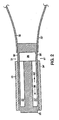
- a piezoelectric ink jet head 2 includes multiple modules 4, 6 which are assembled into a collar element 10 to which is attached a manifold plate 12, and an orifice plate 14. Ink is introduced through the collar 10 to the jet modules which are actuated to jet ink from the orifices 16 on the orifice plate 14.
- An exemplary ink jet head is described in US 5,640,184 , incorporated supra, and is available as Model CCP-256 (Spectra, Inc., Hanover, New Hampahire).
- Each of the ink jet modules 4, 6 includes a body 20, which is formed of a thin rectangular block of a material such as sintered carbon or ceramic. Into both sides of the body are machined a series of wells 22 which form ink pumping chambers. The ink is introduced through an ink fill passage 26 which is also machined into the body.
- the opposing surfaces of the body are covered with flexible polymer films 30, 30' that include a series of electrical contacts arranged to be positioned over the pumping chambers in the body.
- the electrical contacts are connected to leads, which, in turn, can be connected to a flex print 32, 32' including driver integrated circuit 33, 33'.
- the films 30, 30' may be flex prints (Kapton) available from Advanced Circuit Systems located in Franklin, New Hampshire.
- Each flex print film is sealed to the body 20 by a thin layer of epoxy.
- the epoxy layer is thin enough to fill in the surface roughness of the jet body so as to provide a mechanical bond, but also thin enough so that only a small amount of epoxy is squeezed from the bond lines into the pumping chambers.
- Each of the piezoelectric elements 34, 34' which may be a single monolithic PZT member, is positioned over the flex print 30, 30'.
- Each of the piezoelectric elements 34, 34' have electrodes that are formed by chemically etching away conductive metal that has been vacuum vapor deposited onto the surface of the piezoelectric element.
- the electrodes on the piezoelectric element are at locations corresponding to the pumping chambers.
- the electrodes on the piezoelectric element electrically engage the corresponding contacts on the flex print 30, 30', As a result, electrical contact is made to each of the piezoelectric elements on the side of the element in which actuation is effected.
- the piezoelectric elements are fixed to the flex prints by thin layers of epoxy.
- the epoxy thickness is sufficient to fill in the surface roughness of the piezo electric element so as to provide a mechanical bond, but also thin enough so that it does not act as an insulator between the electrodes on the piezoelectric element and the electrodes on the flex print.
- the electrode metallization on the flex print should be thin. It should be less than 25 microns, and less than 10 microns is preferred.
- the piezoelectric elements 34, 34' are sized to cover only the portion of the body that includes the machined ink pumping chambers 22.
- the portion of the body that includes the ink fill passage 26 is not covered by the piezoelectric element.
- the overall size of the piezoelectric element is reduced. Reducing the size of the piezoelectric element reduces cost, and also reduces electrical capacitance of the jet, which reduces jet electrical drive power requirements.
- the flex prints provide chemical isolation between the ink and the piezoelectric element and its electrodes, providing more flexibility in ink design. Inks that are corrosive to metal electrodes and inks that may be adversely affected by exposure to electrical voltages such as water based inks can be used.
- the flex prints also provide electrical isolation between the jet body and the ink, on one hand, and the piezoelectric element and its electrodes on the other hand. This allows simpler designs for jet drive circuitry when the jet body or the ink in the pumping chamber is conductive. In normal use, an operator may come into contact with the orifice plate, which may be in electrical contact with the ink and the jet body. With the electrical isolation provided by the flex print, the drive circuit does not have to accommodate the instance where an operator comes in contact with an element of the drive circuit.
- the ink fill passage 26 is sealed by a portion 31, 31' of the flex print, which is attached to the exterior portion of the module body.
- the flex print forms a non-rigid cover over (and seals) the ink fill passage and approximates a free surface of the fluid exposed to atmosphere. Covering the ink fill passage with a non-rigid flexible surface reduces the crosstalk between jets.
- Crosstalk is unwanted interaction between jets.
- the firing of one or more jets may adversely affect the performance of other jets by altering jet velocities or the drop volumes jetted. This can occur when unwanted energy is transmitted between jets.
- the effect of providing an ink fill passage with the equivalent of a free surface is that more energy is reflected back into the pumping chamber at the fill end of a pumping chamber, and less energy enters the ink fill passage where it could affect the performance of neighboring jets.
- the piezoelectric element In normal operation, the piezoelectric element is actuated first in a manner that increases the volume of the pumping chamber, and then, after a period of time, the piezoelectric element is deactuated so that it returns to its original position.
- Increasing the volume of the pumping chamber causes a negative pressure wave to be launched. This negative pressure starts in the pumping chamber and travels toward both ends of the pumping chamber (towards the orifice and towards the ink fill passage as suggested by arrows 33, 33').
- the negative wave reaches the end of the pumping chamber and encounters the large area of the ink fill passage (which communicates with an approximated free surface), the negative wave is reflected back into the pumping chamber as a positive wave, travelling towards the orifice.
- the returning of the piezoelectric element to its original position also creates a positive wave.
- the timing of the deactuation of the piezoelectric element is such that its positive wave and the reflected positive wave are additive when they reach the orifice. This is discussed in US 4,891,654 , the entire content of which is incorporated herein by reference.
- Reflecting energy back into the pumping chamber increases the pressure at the orifice for a given applied voltage, and reduces the amount of energy transmitted into the fill area which could adversely affect other jets as crosstalk.
- the compliance of the flex print over the fill area also reduces crosstalk between jets by reducing the amplitude of pressure pulses that enter the ink fill area from firing jets. Compliance of a metal layer in another context is discussed in US 4,891,654 .
- the piezoelectric element has electrodes 40 on the side of the piezoelectric element 34 that comes into contact with the flex print.
- Each electrode 40 is placed and sized to correspond to a pumping chamber 45 in the jet body.
- Each electrode 40 has an elongated region 42, having a length and width generally corresponding to that of the pumping chamber, but shorter and narrower such that a gap 43 exists between the perimeter of electrode 40 and the sides and end of the pumping chamber.
- These electrode regions 42 which are centered on the pumping chambers, are the drive electrodes.
- a comb-shaped second electrode 52 on the piezoelectric element generally corresponds to the area outside the pumping chamber. This electrode 52 is the common (ground) electrode.
- the flex print has electrodes 50 on the side 51 of the flex print that comes into contact with the piezoelectric element.
- the flex print electrodes and the piezoelectric element electrodes overlap sufficiently for good electrical contact and easy alignment of the flex print and the piezoelectric element.
- the flex print electrodes extend beyond the piezoelectric element (in the vertical direction in figure 3 ) to allow for a soldered connection to the flex print 32 that contains the driving circuitry. It is not necessary to have two flex prints 30, 32. A single flex print can be used.
- FIGs. 4A and 4B a graphical representation of the field lines in a piezoelectric element and the resulting displacement of the piezoelectric element are shown for a single jet.
- Figure 4A indicates theoretical electric field lines in the piezoelectric element
- Fig. 4B is an exaggeration of the displacement of the piezoelectric element during actuation for illustration purposes.
- the actual displacement of the piezoelectric element is approximately 1/10,000 the thickness of the piezoelectric element (1 millionth of an inch).
- the piezoelectric element is shown with electrodes 70, 71 on the lower surface next to the jet body 72, and air 74 above the piezoelectric element 76.
- the piezoelectric element has a poling field 75 that is substantially uniform and perpendicular to the surface containing the electrodes. When the electric field is applied perpendicularly to the poling field, the piezoelectric element moves in shear mode. When the electric field is applied parallel to the poling field, the piezoelectric element moves in extension mode.
- the displacement of the surface of the piezoelectric element adjacent to the pumping chamber can be substantially greater than if the electrodes were on the opposite surface of the piezoelectric element.
- the bulk of the displacement is due to the shear mode effect, but in this configuration, parasitic extension mode works to increase the displacement.
- the electric field lines are substantially perpendicular to the poling field, resulting in displacement due to shear mode.
- the electric field lines In the material close to the electrodes, the electric field lines have a larger component that is parallel to the poling field, resulting in parasitic extension mode displacement.
- the piezoelectric material In the area of the common electrodes, the piezoelectric material extends in a direction away from the pumping chamber. In the area of the drive electrode, the component of the electric field that is parallel to the poling field is in the opposite direction. This results in compression of the piezoelectric material in the area of the drive electrode. This area around the drive electrode is smaller than the area between the common electrodes. This increases the total displacement of the surface of the piezoelectric element that is next to the pumping chamber.
- the jet body is comprised of multiple parts.
- the frame of the jet body 80 is sintered carbon and contains an ink fill passage.
- stiffening plates 82, 82.' which are thin metal plates designed to stiffen the assembly.
- cavity plates 84, 841 which are thin metal plates into which pumping chambers have been chemically milled.
- Attached to the cavity plates are the flex prints 30, 30', and to the flex prints are attached the piezoelectric elements 34, 34'. All these elements are bonded together with epoxy.
- the flex prints that contain the drive circuitry 32, 32', are attached by a soldering process.
- the jet body is machined from sintered carbon approximately 0.12 inches thick.
- the stiffening plates are chemically milled from 0.007 inch thick kovar metal, with a fill opening 86 per jet that is 0.030 inches by 0.125 inches located over the ink fill passage.
- the cavity plates are chemically milled from 0.006 inch thick kovar metal.
- the pumping chamber openings 88 in the cavity plate are 0.033 inches wide and 0.490 inches long.
- the flex print attached to the piezoelectric element is made from 0.001 inch Kapton, available from The Dupont Company.
- the piezoelectric element is 0.010 inch thick and 0.3875 inches by 2.999 inches.
- the drive electrodes on the piezoelectric element are 0.016 inches wide and 0.352 inches long.
- the separation of the drive electrode from the common electrode is approximately 0.010 inches.
- the above elements are bonded together with epoxy.
- the epoxy bond lines between the flex print and the piezoelectric element have a thickness in the range of 0 to 15 microns. In areas were electrical connection must be made between the flex print and the piezoelectric element, the thickness of the epoxy must be zero at least in some places, and the thickness of the epoxy in other places will depend on surface variations of the flex print and the piezoelectric element.
- the drive circuitry flex print 32 is electrically connected to the flex print 30 attached to the piezoelectric element via a soldering process.
- velocity data is shown for a 256 jet print head of the design in Fig. 5 .
- the velocity data is presented normalized to the average velocity of all the jets.
- Two sets of data are overlaid on the graph. One set is the velocity of a given jet measured when no other jets are firing.
- the other set of data is the velocity of a given jet when all other jets are firing.
- the two sets of data almost completely overlaying one another is an indication of the low crosstalk between jets that this configuration provides.
- the piezoelectric, elements 34, 34' do not have electrodes on their surfaces.
- the flex prints 30, 30' have electrodes that are brought into sufficient contact with the piezoelectric element and are of a shape such that electrodes on the piezoelectric material are not required. This is discussed in US 5,755,909 , the entire content of which is incorporated herein by reference.
- the piezoelectric elements 34, 34 have electrodes only on the surface away from the pumping chambers.
- the piezoelectric elements have drive and common electrodes on the surface away from the pumping chambers, and a common electrode on the side next to the pumping chambers.
- This electrode configuration is more efficient (more piezoelectric element deflection for a given applied voltage) than having electrodes only on the surface of the piezoelectric element away from the pumping chambers.
- This configuration results in some electric field lines going from one surface of the piezoelectric element to the other surface, and hence having a component parallel to the poling field in the piezoelectric element.
- the component of the electric field parallel to the poling field results in extension mode deflection of the piezoelectric element.
- the extension mode deflection of the piezoelectric element causes stress in the plane of the piezoelectric element. Stress in the plane of the piezoelectric element caused by one jet can adversely affect the output of other jets. This adverse effect varies with the number of jets active at a given time, and varies with the frequency that the jets are activated. This is a form of crosstalk. In this embodiment, efficiency is traded for crosstalk.
- the piezoelectric elements 34, 34' have drive and common electrodes on both surfaces.
- the flex print may be made of a wide variety of flexible insulative materials, and the dimensions of the flex print may be any dimensions that will achieve the appropriate degrees of compliance adjacent the ink reservoirs and adjacent the fill passage. In regions where the flex print seals only the fill passage and is not required to provide electrical contact, the flex print could be replaced by a compliant metal layer.
Abstract
Description
- This invention relates to piezoelectric ink jet modules.
- A piezoelectric ink jet module includes a module body, a piezoelectric element, and an electrical connection element for driving the piezoelectric element. The module body, usually carbon or ceramic, is typically a thin, rectangular member into the surfaces of which are machined a series of ink reservoirs that serve as pumping chambers for ink. The piezoelectric element is disposed over the surface of the jet body to cover the pumping chambers and position the piezoelectric material in a manner to pressurize the ink in the pumping chambers to effect jetting.
- In a typical shear mode piezoelectric ink jet module, a single, monolithic piezoelectric element covers the pumping chambers to provide not only the ink pressurizing function but also to seal the pumping chambers against ink leakage. The electrical connection is typically made by a flex print positioned over the exterior surface of the piezoelectric element and provided with electrical contacts at locations corresponding to the locations of the pumping chambers. An example of a piezoelectric shear mode ink jet head is described in
US 5,640,184 , the entire contents of which is incorporated herein by reference. - In one known ink jet module, available from Brother, a resin diaphragm is provided next to each of the pumping chambers. The central region of each diaphragm is pumped by a piezoelectric feature. Electrodes are embedded in the piezoelectric material.
- This invention relates to a piezoelectric ink jet head that includes a polymer, preferably a flex print, located between the piezoelectric element and the pumping chambers in the jet body. The polymer seals the pumping chambers and also positions the electrodes on the side of the piezoelectric element in which motion is effected, which can reduce the magnitude of the drive voltage required for operation. The compliant flex print material also can provide electrical, mechanical, and fluidic pressure isolation between pumping chambers, which improves jetting accuracy.
- Thus, in one aspect, the invention features a piezoelectric element that is positioned to subject the ink within an ink reservoir to jetting pressure. A flexible material carries electrical contacts arranged for activation of said piezoelectric element and is positioned between the reservoir and the piezoelectric element in a manner to seal the reservoir.
- Implementations of the invention may include one or more of the following features. The material may be a polymer. The ink reservoir may be defined by a multi-element module body. An ink fill flow path leading to the reservoir may be sealed by the polymer. The polymer may include an area that is not supported. The piezoelectric element may be sized to cover the reservoir without covering the ink fill flow path. The module may include a series of reservoirs all covered by a single piezoelectric element, or in other examples by separate respective piezoelectric elements. The module may be a shear mode piezoelectric module. The piezoelectric element may be a monolithic piezoelectric member.
- In other general aspects of the invention, the flexible material over the flow path contains an area that is not supported; the piezoelectric element spans the ink reservoir and is positioned to subject the ink within the reservoir to jetting pressure; and electrical contacts are located only on a side of the piezoelectric element adjacent to the ink reservoir. In some implementations, the contacts may be thinner than 25 microns, preferably thinner than 10 microns.
- Other features and advantages will become apparent from the following description and from the claims.
- We first briefly describe the drawings.
-
Fig. 1 is an exploded view of a shear mode piezoelectric ink jet print head; -
Fig. 2 is a cross-sectional side view through an ink jet module; -
Fig. 3 is a perspective view of an ink jet module illustrating the location of electrodes relative to the pumping chamber and piezoelectric element; -
Fig. 4A is a graph of the field lines in a piezo electric element, whileFig. 4B illustrates element displacement when a driving voltage is applied; -
Fig. 5 is an exploded view of another embodiment of an ink jet module; -
Fig. 6 is a graph of jet velocity data for a 256 jet embodiment of the print head. - Referring to
Fig. 1 , a piezoelectric ink jet head 2 includesmultiple modules collar element 10 to which is attached amanifold plate 12, and anorifice plate 14. Ink is introduced through thecollar 10 to the jet modules which are actuated to jet ink from theorifices 16 on theorifice plate 14. An exemplary ink jet head is described inUS 5,640,184 , incorporated supra, and is available as Model CCP-256 (Spectra, Inc., Hanover, New Hampahire). - Each of the
ink jet modules body 20, which is formed of a thin rectangular block of a material such as sintered carbon or ceramic. Into both sides of the body are machined a series ofwells 22 which form ink pumping chambers. The ink is introduced through anink fill passage 26 which is also machined into the body. - The opposing surfaces of the body are covered with
flexible polymer films flex print circuit 33, 33'. Thefilms body 20 by a thin layer of epoxy. The epoxy layer is thin enough to fill in the surface roughness of the jet body so as to provide a mechanical bond, but also thin enough so that only a small amount of epoxy is squeezed from the bond lines into the pumping chambers. - Each of the
piezoelectric elements 34, 34', which may be a single monolithic PZT member, is positioned over theflex print piezoelectric elements 34, 34' have electrodes that are formed by chemically etching away conductive metal that has been vacuum vapor deposited onto the surface of the piezoelectric element. The electrodes on the piezoelectric element are at locations corresponding to the pumping chambers. The electrodes on the piezoelectric element electrically engage the corresponding contacts on theflex print - Referring to
Fig. 2 , thepiezoelectric elements 34, 34' are sized to cover only the portion of the body that includes the machinedink pumping chambers 22. The portion of the body that includes theink fill passage 26 is not covered by the piezoelectric element. Thus the overall size of the piezoelectric element is reduced. Reducing the size of the piezoelectric element reduces cost, and also reduces electrical capacitance of the jet, which reduces jet electrical drive power requirements. - The flex prints provide chemical isolation between the ink and the piezoelectric element and its electrodes, providing more flexibility in ink design. Inks that are corrosive to metal electrodes and inks that may be adversely affected by exposure to electrical voltages such as water based inks can be used.
- The flex prints also provide electrical isolation between the jet body and the ink, on one hand, and the piezoelectric element and its electrodes on the other hand. This allows simpler designs for jet drive circuitry when the jet body or the ink in the pumping chamber is conductive. In normal use, an operator may come into contact with the orifice plate, which may be in electrical contact with the ink and the jet body. With the electrical isolation provided by the flex print, the drive circuit does not have to accommodate the instance where an operator comes in contact with an element of the drive circuit.
- The
ink fill passage 26 is sealed by aportion 31, 31' of the flex print, which is attached to the exterior portion of the module body. The flex print forms a non-rigid cover over (and seals) the ink fill passage and approximates a free surface of the fluid exposed to atmosphere. Covering the ink fill passage with a non-rigid flexible surface reduces the crosstalk between jets. - Crosstalk is unwanted interaction between jets. The firing of one or more jets may adversely affect the performance of other jets by altering jet velocities or the drop volumes jetted. This can occur when unwanted energy is transmitted between jets. The effect of providing an ink fill passage with the equivalent of a free surface is that more energy is reflected back into the pumping chamber at the fill end of a pumping chamber, and less energy enters the ink fill passage where it could affect the performance of neighboring jets.
- In normal operation, the piezoelectric element is actuated first in a manner that increases the volume of the pumping chamber, and then, after a period of time, the piezoelectric element is deactuated so that it returns to its original position. Increasing the volume of the pumping chamber causes a negative pressure wave to be launched. This negative pressure starts in the pumping chamber and travels toward both ends of the pumping chamber (towards the orifice and towards the ink fill passage as suggested by
arrows 33, 33'). When the negative wave reaches the end of the pumping chamber and encounters the large area of the ink fill passage (which communicates with an approximated free surface), the negative wave is reflected back into the pumping chamber as a positive wave, travelling towards the orifice. The returning of the piezoelectric element to its original position also creates a positive wave. The timing of the deactuation of the piezoelectric element is such that its positive wave and the reflected positive wave are additive when they reach the orifice. This is discussed inUS 4,891,654 , the entire content of which is incorporated herein by reference. - Reflecting energy back into the pumping chamber increases the pressure at the orifice for a given applied voltage, and reduces the amount of energy transmitted into the fill area which could adversely affect other jets as crosstalk.
- The compliance of the flex print over the fill area also reduces crosstalk between jets by reducing the amplitude of pressure pulses that enter the ink fill area from firing jets. Compliance of a metal layer in another context is discussed in
US 4,891,654 . - Referring to
Fig. 3 , theelectrode pattern 50 on theflex print 30 relative to the pumping chamber and piezoelectric element is illustrated. The piezoelectric element haselectrodes 40 on the side of thepiezoelectric element 34 that comes into contact with the flex print. Eachelectrode 40 is placed and sized to correspond to apumping chamber 45 in the jet body. Eachelectrode 40 has an elongatedregion 42, having a length and width generally corresponding to that of the pumping chamber, but shorter and narrower such that agap 43 exists between the perimeter ofelectrode 40 and the sides and end of the pumping chamber. Theseelectrode regions 42, which are centered on the pumping chambers, are the drive electrodes. A comb-shapedsecond electrode 52 on the piezoelectric element generally corresponds to the area outside the pumping chamber. Thiselectrode 52 is the common (ground) electrode. - The flex print has
electrodes 50 on theside 51 of the flex print that comes into contact with the piezoelectric element. The flex print electrodes and the piezoelectric element electrodes overlap sufficiently for good electrical contact and easy alignment of the flex print and the piezoelectric element. The flex print electrodes extend beyond the piezoelectric element (in the vertical direction infigure 3 ) to allow for a soldered connection to theflex print 32 that contains the driving circuitry. It is not necessary to have twoflex prints - Referring to
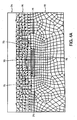
Figs. 4A and4B , a graphical representation of the field lines in a piezoelectric element and the resulting displacement of the piezoelectric element are shown for a single jet.Figure 4A indicates theoretical electric field lines in the piezoelectric element, andFig. 4B is an exaggeration of the displacement of the piezoelectric element during actuation for illustration purposes. The actual displacement of the piezoelectric element is approximately 1/10,000 the thickness of the piezoelectric element (1 millionth of an inch). InFig. 4A , the piezoelectric element is shown withelectrodes jet body 72, and air 74 above thepiezoelectric element 76. For simplicity, the kapton flex print between the piezoelectric element and jet body is not shown in this view. Thedrive electrodes 70 are centered on thepumping chambers 78, and the ground electrode is located just outside the pumping chambers. Application of a drive voltage to the drive electrode results inelectric field lines 73 as shown inFig. 4A . The piezoelectric element has a polingfield 75 that is substantially uniform and perpendicular to the surface containing the electrodes. When the electric field is applied perpendicularly to the poling field, the piezoelectric element moves in shear mode. When the electric field is applied parallel to the poling field, the piezoelectric element moves in extension mode. In this configuration with ground and drive electrodes on the side of the piezoelectric element that is next to the pumping chambers, for a given applied voltage, the displacement of the surface of the piezoelectric element adjacent to the pumping chamber can be substantially greater than if the electrodes were on the opposite surface of the piezoelectric element. - The bulk of the displacement is due to the shear mode effect, but in this configuration, parasitic extension mode works to increase the displacement. In the piezoelectric element, in the material between the common and the derive electrodes the electric field lines are substantially perpendicular to the poling field, resulting in displacement due to shear mode. In the material close to the electrodes, the electric field lines have a larger component that is parallel to the poling field, resulting in parasitic extension mode displacement. In the area of the common electrodes, the piezoelectric material extends in a direction away from the pumping chamber. In the area of the drive electrode, the component of the electric field that is parallel to the poling field is in the opposite direction. This results in compression of the piezoelectric material in the area of the drive electrode. This area around the drive electrode is smaller than the area between the common electrodes. This increases the total displacement of the surface of the piezoelectric element that is next to the pumping chamber.
- Overall, more displacement may be achieved from a given drive voltage if the electrodes are on the pumping chamber side of the piezoelectric element, rather than on the opposite side of the piezoelectric element. In embodiments, this improvement may be achieved without incurring the expense of placing electrodes on both sides of the piezoelectric element.
- Referring to
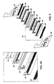
Fig. 5 , another embodiment of a jet module is shown. In this embodiment, the jet body is comprised of multiple parts. The frame of thejet body 80 is sintered carbon and contains an ink fill passage. Attached to the jet body on each side are stiffeningplates cavity plates 84, 841, which are thin metal plates into which pumping chambers have been chemically milled. Attached to the cavity plates are the flex prints 30, 30', and to the flex prints are attached thepiezoelectric elements 34, 34'. All these elements are bonded together with epoxy. The flex prints that contain thedrive circuitry - Describing the embodiment shown in
Fig. 5 in more detail, the jet body is machined from sintered carbon approximately 0.12 inches thick. The stiffening plates are chemically milled from 0.007 inch thick kovar metal, with a fill opening 86 per jet that is 0.030 inches by 0.125 inches located over the ink fill passage. The cavity plates are chemically milled from 0.006 inch thick kovar metal. Thepumping chamber openings 88 in the cavity plate are 0.033 inches wide and 0.490 inches long. The flex print attached to the piezoelectric element is made from 0.001 inch Kapton, available from The Dupont Company. The piezoelectric element is 0.010 inch thick and 0.3875 inches by 2.999 inches. The drive electrodes on the piezoelectric element are 0.016 inches wide and 0.352 inches long. The separation of the drive electrode from the common electrode is approximately 0.010 inches. The above elements are bonded together with epoxy. The epoxy bond lines between the flex print and the piezoelectric element have a thickness in the range of 0 to 15 microns. In areas were electrical connection must be made between the flex print and the piezoelectric element, the thickness of the epoxy must be zero at least in some places, and the thickness of the epoxy in other places will depend on surface variations of the flex print and the piezoelectric element. The drivecircuitry flex print 32 is electrically connected to theflex print 30 attached to the piezoelectric element via a soldering process. - Referring to
Fig. 6 , velocity data is shown for a 256 jet print head of the design inFig. 5 . The velocity data is presented normalized to the average velocity of all the jets. Two sets of data are overlaid on the graph. One set is the velocity of a given jet measured when no other jets are firing. The other set of data is the velocity of a given jet when all other jets are firing. The two sets of data almost completely overlaying one another is an indication of the low crosstalk between jets that this configuration provides. - In another embodiment, the piezoelectric,
elements 34, 34' do not have electrodes on their surfaces. The flex prints 30, 30' have electrodes that are brought into sufficient contact with the piezoelectric element and are of a shape such that electrodes on the piezoelectric material are not required. This is discussed inUS 5,755,909 , the entire content of which is incorporated herein by reference. - In another embodiment, the
piezoelectric elements - In another embodiment, the piezoelectric elements have drive and common electrodes on the surface away from the pumping chambers, and a common electrode on the side next to the pumping chambers. This electrode configuration is more efficient (more piezoelectric element deflection for a given applied voltage) than having electrodes only on the surface of the piezoelectric element away from the pumping chambers.
- This configuration results in some electric field lines going from one surface of the piezoelectric element to the other surface, and hence having a component parallel to the poling field in the piezoelectric element. The component of the electric field parallel to the poling field results in extension mode deflection of the piezoelectric element. With this electrode configuration, the extension mode deflection of the piezoelectric element causes stress in the plane of the piezoelectric element. Stress in the plane of the piezoelectric element caused by one jet can adversely affect the output of other jets. This adverse effect varies with the number of jets active at a given time, and varies with the frequency that the jets are activated. This is a form of crosstalk. In this embodiment, efficiency is traded for crosstalk.
- In the embodiment with electrodes on the surface of the piezoelectric element adjacent to the pumping chambers, no efficiency is gained from adding a ground electrode on the surface of the piezoelectric element away from the pumping chambers. Adding a ground electrode to the surface of the piezoelectric element away from the pumping chamber will increase the electrical capacitance of the jet and so will increase the electrical drive requirements.
- In another embodiment, the
piezoelectric elements 34, 34' have drive and common electrodes on both surfaces. - Still other embodiments are within the scope of the following claims. For example, the flex print may be made of a wide variety of flexible insulative materials, and the dimensions of the flex print may be any dimensions that will achieve the appropriate degrees of compliance adjacent the ink reservoirs and adjacent the fill passage. In regions where the flex print seals only the fill passage and is not required to provide electrical contact, the flex print could be replaced by a compliant metal layer.
- Although the present invention has been described above, and is defined in the appended claims, it is to be understood that the invention can also be defined in accordance with the following embodiments:
- 1. A piezoelectric ink jet module, comprising an ink reservoir, a piezoelectric element positioned to subject the ink within the reservoir to jetting pressure, and a flexible material that carries electrical contacts arranged for activation of said piezoelectric element and is positioned between the reservoir and the piezoelectric element in a manner to seal the reservoir.
- 2. The module of embodiment 1 in which the material comprises a polymer.
- 3. The module of embodiment 1 in which the ink reservoir is defined by a module body.
- 4. The module of embodiment 3 in which the body comprises a multi-element structure.
- 5. The module of embodiment 1 further comprising an ink fill flow path leading to said reservoir and wherein said polymer seals said flow path.
- 6. The module of embodiment 5 in which the polymer includes an area that is not supported.
- 7. The module of embodiment 5 wherein said piezoelectric element is sized to cover said reservoir without covering said ink fill flow path.
- 8. The module of embodiment 1 wherein said module includes a series of reservoirs.
- 9. The module of embodiment 8 wherein all of said reservoirs are covered by a single piezoelectric element.
- 10. The module of embodiment 5 wherein said reservoirs are covered by separate respective piezoelectric elements.
- 11. The module of embodiment 1 wherein said module comprises a shear mode piezoelectric module.
- 12. The module of embodiment 1 wherein said piezoelectric element comprises a monolithic piezoelectric member.
- 13. A piezoelectric ink jet module, comprising: an ink reservoir, an ink fill flow path, a piezoelectric element positioned adjacent said reservoir so that ink within the reservoir can be subject to jetting pressure, and a flexible material positioned over the flow path that contains an area or areas that are not supported.
- 14. The module of embodiment 13 in which the ink reservoir is defined by a module body.
- 15. The module of
embodiment 14 in which the body comprises a multi-element structure. - 16. The module of embodiment 13 wherein the piezoelectric element comprises a shear mode piezoelectric module.
- 17. The module of embodiment 13 wherein the flexible material comprises a flex print including electrical contacts arranged for activation of said piezoelectric element.
- 18. The module of
embodiment 10 wherein the body defines an ink fill flow path leading to said reservoir and said polymer film seals said flow path. - 19. The module of embodiment 13 wherein said piezoelectric element is sized to cover said reservoir without covering said ink fill flow path.
- 20. An ink jet head comprising ink jet modules, each of the inkjet modules comprising an ink reservoir, a piezoelectric element positioned to subject the ink within the reservoir to jetting pressure, and a flexible material that carries electrical contacts arranged for activation of said piezoelectric element and is positioned between the reservoir and the piezoelectric element in a manner to seal the reservoir.
- 21. A method for use in making a piezoelectric ink jet module, comprising positioning a piezoelectric element to subject the ink within an ink reservoir to jetting pressure, and positioning a flexible material that carries electrical contacts arranged for activation of said piezoelectric element between the reservoir and the piezoelectric element in a manner to seal the reservoir.
- 22. A piezoelectric ink jet module, comprising an ink reservoir, a piezoelectric element that spans the ink reservoir and is positioned to subject the ink within the reservoir to jetting pressure, and a flexible material that is positioned between the reservoir and the piezoelectric element in a manner to seal the reservoir.
- 23. The module of
embodiment 22 in which the flexible material carries electrical contacts arranged for activation of said piezoelectric element. - 24. The module of
embodiment 22 in which the material comprises a polymer. - 25. The module of
embodiment 22 in which the ink reservoir is defined by a module body. - 26. The module of embodiment 25 in which the body comprises a multi-element structure.
- 27. The module of
embodiment 22 further comprising an ink fill flow path leading to said reservoir and wherein said polymer seals said flow path. - 28. The module of
embodiment 22 in which the polymer includes an area that is not supported. - 29. The module of embodiment 28 wherein said piezoelectric element is sized to cover said reservoir without covering said ink fill flow path.
- 30. The module of
embodiment 22 wherein said module includes a series of reservoirs. - 31. The module of
embodiment 30 wherein all of said reservoirs are covered by a single piezoelectric element. - 32. The module of
embodiment 30 wherein said reservoirs are covered by separate respective piezoelectric elements. - 33. The module of
embodiment 22 wherein said module comprises a shear mode piezoelectric module. - 34. The module of
embodiment 22 wherein said piezoelectric element comprises a monolithic piezoelectric member. - 35. A piezoelectric ink jet module, comprising an ink reservoir, a piezoelectric element positioned to subject the ink within the reservoir to jetting pressure, and which has electrical connections only on the side of the piezoelectric element adjacent to the ink reservoir.
- 36. The module of embodiment 35 in which the ink reservoir is defined by a module body.
- 37. The module of embodiment 35 in which the body comprises a multi-element structure.
- 38. The module of embodiment 35 wherein said piezoelectric element is sized to cover said reservoir without covering said ink fill flow path.
- 39. The module of embodiment 35 wherein said module includes a series of reservoirs.
- 40. The module of embodiment 35 wherein all of said reservoirs are covered by a single piezoelectric element.
- 41. The module of embodiment 35 wherein said reservoirs are covered by separate respective piezoelectric elements.
- 42. The module of embodiment 35 wherein said module comprises a shear mode piezoelectric module.
- 43. The module of embodiment 35 wherein said piezoelectric element comprises a monolithic piezoelectric member.
- 44. The module of embodiments 17,21,23 or 35 in which the electrical contacts are formed as a metallization layer that is thinner than 25 microns, preferably thinner than 10 microns.
Claims (16)
- A piezoelectric ink jet module, comprising
an ink reservoir,
a piezoelectric element positioned to subject the ink within the reservoir to jetting pressure, and
a flexible material that carries electrical contacts arranged for activation of said piezoelectric element. - The module of claim 1 in which the material comprises a polymer.
- The module of one of the preceding claims, further comprising a jet body (80) containing an ink fill passage leading to the ink reservoir.
- The module of one of the preceding claims, further comprising a stiffening plate (82, 82') attached to the jet body (80).
- The module of claim 4, wherein the stiffening plate is a metal plate.
- The module of claim 4 or 5, wherein the stiffening plate has a fill opening (86) located over the ink fill passage.
- The module of one of the preceding claims, further comprising a cavity plate (84, 84') containing the ink reservoir.
- The module of claim 7, wherein the flexible material is attached to the cavity plate (84, 84').
- The module of claim 7 or 8, wherein the cavity plate (84, 84') is attached to the stiffening plate (82, 82').
- The module of one of claims 7 to 9, wherein the cavity plate (84, 84') is a metal plate.
- The module of one of the preceding claims, wherein the flexible material is attached to the piezoelectric element.
- The module of one of the preceding claims, wherein the flexible material is positioned between the reservoir and the piezoelectric element in a manner to seal the reservoir.
- The module of one of the preceding claims, wherein the multiple parts of the ink jet module are bonded together with epoxy.
- The module of one of the preceding claims, wherein the jet body (80) is formed of sintered carbon or ceramic.
- An ink jet head comprising ink jet modules, each of the ink jet modules comprising
an ink reservoir, a piezoelectric element positioned to subject the ink within the reservoir to jetting pressure, and
a flexible material that carries electrical contacts arranged for activation of said piezoelectric element. - A method for use in making a piezoelectric ink jet module, comprising positioning a piezoelectric element to subject the ink within an ink reservoir to jetting pressure, and
positioning a flexible material that carries electrical contacts arranged for activation of said piezoelectric element.
Priority Applications (1)
| Application Number | Priority Date | Filing Date | Title |
|---|---|---|---|
| EP10176589A EP2253473B1 (en) | 1999-10-05 | 2000-10-05 | Piezoelectric ink jet module |
Applications Claiming Priority (3)
| Application Number | Priority Date | Filing Date | Title |
|---|---|---|---|
| US09/412,827 US6755511B1 (en) | 1999-10-05 | 1999-10-05 | Piezoelectric ink jet module with seal |
| EP00981005A EP1218189B1 (en) | 1999-10-05 | 2000-10-05 | Piezoelectric ink jet module with seal |
| EP06015045A EP1752295B1 (en) | 1999-10-05 | 2000-10-05 | Piezoelectric ink jet module |
Related Parent Applications (1)
| Application Number | Title | Priority Date | Filing Date |
|---|---|---|---|
| EP06015045A Division EP1752295B1 (en) | 1999-10-05 | 2000-10-05 | Piezoelectric ink jet module |
Publications (1)
| Publication Number | Publication Date |
|---|---|
| EP2088000A1 true EP2088000A1 (en) | 2009-08-12 |
Family
ID=23634669
Family Applications (5)
| Application Number | Title | Priority Date | Filing Date |
|---|---|---|---|
| EP10176589A Expired - Lifetime EP2253473B1 (en) | 1999-10-05 | 2000-10-05 | Piezoelectric ink jet module |
| EP06015045A Expired - Lifetime EP1752295B1 (en) | 1999-10-05 | 2000-10-05 | Piezoelectric ink jet module |
| EP00981005A Expired - Lifetime EP1218189B1 (en) | 1999-10-05 | 2000-10-05 | Piezoelectric ink jet module with seal |
| EP09161286A Ceased EP2088000A1 (en) | 1999-10-05 | 2000-10-05 | Piezoelectric ink jet module |
| EP04004742A Expired - Lifetime EP1439065B1 (en) | 1999-10-05 | 2000-10-05 | Piezoelectric ink jet printing module |
Family Applications Before (3)
| Application Number | Title | Priority Date | Filing Date |
|---|---|---|---|
| EP10176589A Expired - Lifetime EP2253473B1 (en) | 1999-10-05 | 2000-10-05 | Piezoelectric ink jet module |
| EP06015045A Expired - Lifetime EP1752295B1 (en) | 1999-10-05 | 2000-10-05 | Piezoelectric ink jet module |
| EP00981005A Expired - Lifetime EP1218189B1 (en) | 1999-10-05 | 2000-10-05 | Piezoelectric ink jet module with seal |
Family Applications After (1)
| Application Number | Title | Priority Date | Filing Date |
|---|---|---|---|
| EP04004742A Expired - Lifetime EP1439065B1 (en) | 1999-10-05 | 2000-10-05 | Piezoelectric ink jet printing module |
Country Status (7)
| Country | Link |
|---|---|
| US (4) | US6755511B1 (en) |
| EP (5) | EP2253473B1 (en) |
| JP (2) | JP2003511264A (en) |
| CA (1) | CA2386737C (en) |
| DE (3) | DE60032496T2 (en) |
| HK (3) | HK1069150A1 (en) |
| WO (1) | WO2001025018A2 (en) |
Families Citing this family (33)
| Publication number | Priority date | Publication date | Assignee | Title |
|---|---|---|---|---|
| US6755511B1 (en) * | 1999-10-05 | 2004-06-29 | Spectra, Inc. | Piezoelectric ink jet module with seal |
| US20020085067A1 (en) * | 2000-12-29 | 2002-07-04 | Robert Palifka | Ink jet printing module |
| US7052117B2 (en) | 2002-07-03 | 2006-05-30 | Dimatix, Inc. | Printhead having a thin pre-fired piezoelectric layer |
| US6878643B2 (en) * | 2002-12-18 | 2005-04-12 | The Regents Of The University Of California | Electronic unit integrated into a flexible polymer body |
| JP4211475B2 (en) * | 2003-04-28 | 2009-01-21 | パナソニック株式会社 | Ink jet head unit and ink jet recording apparatus equipped with the same |
| DE112004000028T5 (en) * | 2003-04-28 | 2006-04-20 | Matsushita Electric Industrial Co., Ltd., Kadoma | Inkjet recording device |
| US8753702B2 (en) | 2004-01-20 | 2014-06-17 | Fujifilm Dimatix, Inc. | Printing on edible substrates |
| US20080075859A1 (en) | 2004-01-20 | 2008-03-27 | Baker Richard J | Printing, Depositing, or Coating On Flowable Substrates |
| US7281778B2 (en) * | 2004-03-15 | 2007-10-16 | Fujifilm Dimatix, Inc. | High frequency droplet ejection device and method |
| US8491076B2 (en) | 2004-03-15 | 2013-07-23 | Fujifilm Dimatix, Inc. | Fluid droplet ejection devices and methods |
| JP5004806B2 (en) * | 2004-12-30 | 2012-08-22 | フジフィルム ディマティックス, インコーポレイテッド | Inkjet printing method |
| JP4258668B2 (en) * | 2006-05-08 | 2009-04-30 | セイコーエプソン株式会社 | Liquid ejecting head and liquid ejecting apparatus |
| WO2008105792A2 (en) * | 2006-06-24 | 2008-09-04 | Qd Vision, Inc. | Methods for depositing nanomaterial, methods for fabricating a device, methods for fabricating an array of devices and compositions |
| WO2008108798A2 (en) | 2006-06-24 | 2008-09-12 | Qd Vision, Inc. | Methods for depositing nanomaterial, methods for fabricating a device, and methods for fabricating an array of devices |
| US7988247B2 (en) | 2007-01-11 | 2011-08-02 | Fujifilm Dimatix, Inc. | Ejection of drops having variable drop size from an ink jet printer |
| JP5773646B2 (en) | 2007-06-25 | 2015-09-02 | キユーデイー・ビジヨン・インコーポレーテツド | Compositions and methods comprising depositing nanomaterials |
| US20110122587A1 (en) * | 2008-05-21 | 2011-05-26 | Deming Stephen R | Flexible circuit stretching |
| CN103552379B (en) * | 2008-05-22 | 2015-09-02 | 富士胶片株式会社 | Fluid ejection apparatus |
| US8057003B2 (en) * | 2008-05-23 | 2011-11-15 | Fujifilm Dimatix, Inc. | Method and apparatus to provide variable drop size ejection with a low power waveform |
| US8025353B2 (en) * | 2008-05-23 | 2011-09-27 | Fujifilm Dimatix, Inc. | Process and apparatus to provide variable drop size ejection with an embedded waveform |
| US8608267B2 (en) * | 2008-06-30 | 2013-12-17 | Fujifilm Dimatix, Inc. | Ink jetting |
| US8807716B2 (en) * | 2008-06-30 | 2014-08-19 | Fujifilm Dimatix, Inc. | Ink delivery |
| WO2010002569A1 (en) * | 2008-06-30 | 2010-01-07 | Fujifilm Dimatix, Inc. | Ink jetting |
| US8480196B2 (en) * | 2009-10-23 | 2013-07-09 | Fujifilm Dimatix, Inc. | Method and apparatus to eject drops having straight trajectories |
| JP5650049B2 (en) | 2010-07-29 | 2015-01-07 | 富士フイルム株式会社 | Inkjet recording method and printed matter |
| JP5616811B2 (en) | 2010-07-29 | 2014-10-29 | 富士フイルム株式会社 | Inkjet recording method and printed matter |
| JP5228034B2 (en) | 2010-12-28 | 2013-07-03 | 富士フイルム株式会社 | Ink set for ink jet recording, ink jet recording method and printed matter |
| JP5244899B2 (en) | 2010-12-28 | 2013-07-24 | 富士フイルム株式会社 | Ink composition, inkjet recording method, and printed matter |
| JP5349628B2 (en) | 2011-02-08 | 2013-11-20 | 富士フイルム株式会社 | Inkjet recording method and printed matter |
| JP5486556B2 (en) | 2011-06-28 | 2014-05-07 | 富士フイルム株式会社 | Ink composition, ink container, and ink jet recording method |
| EP2822770B1 (en) * | 2012-03-05 | 2020-04-22 | Fujifilm Dimatix, Inc. | Printhead stiffening |
| JP5654535B2 (en) | 2012-08-29 | 2015-01-14 | 富士フイルム株式会社 | Inkjet recording method and printed matter |
| JP6306991B2 (en) * | 2014-09-19 | 2018-04-04 | 株式会社東芝 | Inkjet head and printer |
Citations (9)
| Publication number | Priority date | Publication date | Assignee | Title |
|---|---|---|---|---|
| US4516140A (en) | 1983-12-27 | 1985-05-07 | At&T Teletype Corporation | Print head actuator for an ink jet printer |
| US4584590A (en) | 1982-05-28 | 1986-04-22 | Xerox Corporation | Shear mode transducer for drop-on-demand liquid ejector |
| US4695854A (en) | 1986-07-30 | 1987-09-22 | Pitney Bowes Inc. | External manifold for ink jet array |
| EP0486256A2 (en) | 1990-11-13 | 1992-05-20 | Citizen Watch Co., Ltd. | Printing head for ink-jet printer |
| EP0667239A2 (en) | 1994-02-15 | 1995-08-16 | Rohm Co., Ltd. | Ink jet printing head |
| US5581288A (en) | 1992-03-06 | 1996-12-03 | Seiko Precision Inc. | Ink jet head block |
| EP0839655A2 (en) | 1992-08-26 | 1998-05-06 | Seiko Epson Corporation | Multi-layer ink jet recording head |
| EP0855273A2 (en) | 1997-01-24 | 1998-07-29 | Seiko Epson Corporation | Ink jet type recording head |
| EP0916497A2 (en) | 1997-11-06 | 1999-05-19 | Seiko Epson Corporation | Ink-jet recording head |
Family Cites Families (35)
| Publication number | Priority date | Publication date | Assignee | Title |
|---|---|---|---|---|
| US4339763A (en) | 1970-06-29 | 1982-07-13 | System Industries, Inc. | Apparatus for recording with writing fluids and drop projection means therefor |
| US3946398A (en) | 1970-06-29 | 1976-03-23 | Silonics, Inc. | Method and apparatus for recording with writing fluids and drop projection means therefor |
| SE349676B (en) * | 1971-01-11 | 1972-10-02 | N Stemme | |
| US4216483A (en) | 1977-11-16 | 1980-08-05 | Silonics, Inc. | Linear array ink jet assembly |
| JPS60159064A (en) * | 1983-12-27 | 1985-08-20 | エーテイーアンドテイー テレタイプ コーポレーシヨン | Actuator for printing head of ink jet printer |
| US4891654A (en) | 1987-09-09 | 1990-01-02 | Spectra, Inc. | Ink jet array |
| JP3125299B2 (en) * | 1989-09-05 | 2001-01-15 | セイコーエプソン株式会社 | Recording head for inkjet printer |
| JPH03166951A (en) * | 1989-11-25 | 1991-07-18 | Seiko Epson Corp | Ink jet head |
| JPH04185348A (en) | 1990-11-17 | 1992-07-02 | Seiko Epson Corp | Liquid jet head and manufacture thereof |
| US5265315A (en) * | 1990-11-20 | 1993-11-30 | Spectra, Inc. | Method of making a thin-film transducer ink jet head |
| JPH05169654A (en) * | 1991-12-20 | 1993-07-09 | Seiko Epson Corp | Ink jet recording head and its manufacturing method |
| US5874974A (en) * | 1992-04-02 | 1999-02-23 | Hewlett-Packard Company | Reliable high performance drop generator for an inkjet printhead |
| JP3144948B2 (en) * | 1992-05-27 | 2001-03-12 | 日本碍子株式会社 | Inkjet print head |
| JP3144949B2 (en) * | 1992-05-27 | 2001-03-12 | 日本碍子株式会社 | Piezoelectric / electrostrictive actuator |
| JPH06238888A (en) | 1993-02-22 | 1994-08-30 | Brother Ind Ltd | Ink ejector |
| JPH06320723A (en) * | 1993-05-12 | 1994-11-22 | Seiko Epson Corp | Ink jet head |
| US5652609A (en) * | 1993-06-09 | 1997-07-29 | J. David Scholler | Recording device using an electret transducer |
| GB9318985D0 (en) | 1993-09-14 | 1993-10-27 | Xaar Ltd | Passivation of ceramic piezoelectric ink jet print heads |
| EP0667329A1 (en) | 1994-02-11 | 1995-08-16 | ENICHEM S.p.A. | Integrated process for the simultaneous production of alkyl tert-butyl ethers and 1-butene |
| JPH07241989A (en) * | 1994-03-08 | 1995-09-19 | Rohm Co Ltd | Ink jet print head |
| US5659346A (en) * | 1994-03-21 | 1997-08-19 | Spectra, Inc. | Simplified ink jet head |
| JPH07304173A (en) * | 1994-05-16 | 1995-11-21 | Fuji Electric Co Ltd | Ink jet recording head |
| DE59509149D1 (en) * | 1994-08-03 | 2001-05-10 | Francotyp Postalia Gmbh | Arrangement for plate-shaped piezo actuators and method for their production |
| JP3570447B2 (en) * | 1994-12-21 | 2004-09-29 | セイコーエプソン株式会社 | Laminated inkjet recording head, method of manufacturing the same, and recording apparatus |
| JP3663652B2 (en) | 1995-02-13 | 2005-06-22 | ブラザー工業株式会社 | Inkjet printer head |
| JP3402349B2 (en) * | 1996-01-26 | 2003-05-06 | セイコーエプソン株式会社 | Ink jet recording head |
| JP3555638B2 (en) * | 1996-04-05 | 2004-08-18 | セイコーエプソン株式会社 | Ink jet recording head |
| EP1118467B1 (en) * | 1996-04-10 | 2006-01-25 | Seiko Epson Corporation | Ink jet recording head |
| JPH09314831A (en) * | 1996-05-23 | 1997-12-09 | Brother Ind Ltd | Ink jet recording head |
| US5755909A (en) | 1996-06-26 | 1998-05-26 | Spectra, Inc. | Electroding of ceramic piezoelectric transducers |
| JP3290897B2 (en) * | 1996-08-19 | 2002-06-10 | ブラザー工業株式会社 | Inkjet head |
| US5901425A (en) * | 1996-08-27 | 1999-05-11 | Topaz Technologies Inc. | Inkjet print head apparatus |
| JP2000127384A (en) * | 1998-10-22 | 2000-05-09 | Brother Ind Ltd | Ink jet head and piezoelectric element |
| US6345880B1 (en) * | 1999-06-04 | 2002-02-12 | Eastman Kodak Company | Non-wetting protective layer for ink jet print heads |
| US6755511B1 (en) * | 1999-10-05 | 2004-06-29 | Spectra, Inc. | Piezoelectric ink jet module with seal |
-
1999
- 1999-10-05 US US09/412,827 patent/US6755511B1/en not_active Expired - Lifetime
-
2000
- 2000-10-05 EP EP10176589A patent/EP2253473B1/en not_active Expired - Lifetime
- 2000-10-05 CA CA002386737A patent/CA2386737C/en not_active Expired - Lifetime
- 2000-10-05 EP EP06015045A patent/EP1752295B1/en not_active Expired - Lifetime
- 2000-10-05 EP EP00981005A patent/EP1218189B1/en not_active Expired - Lifetime
- 2000-10-05 JP JP2001527993A patent/JP2003511264A/en active Pending
- 2000-10-05 WO PCT/US2000/041084 patent/WO2001025018A2/en active IP Right Grant
- 2000-10-05 DE DE60032496T patent/DE60032496T2/en not_active Expired - Lifetime
- 2000-10-05 DE DE60029262T patent/DE60029262T2/en not_active Expired - Lifetime
- 2000-10-05 EP EP09161286A patent/EP2088000A1/en not_active Ceased
- 2000-10-05 EP EP04004742A patent/EP1439065B1/en not_active Expired - Lifetime
- 2000-10-05 DE DE60042504T patent/DE60042504D1/en not_active Expired - Lifetime
-
2004
- 2004-06-28 US US10/879,689 patent/US7011396B2/en not_active Expired - Lifetime
-
2005
- 2005-01-21 HK HK05100578A patent/HK1069150A1/en not_active IP Right Cessation
-
2006
- 2006-01-20 US US11/336,423 patent/US7478899B2/en not_active Expired - Fee Related
-
2007
- 2007-07-27 HK HK07108261.8A patent/HK1100366A1/en not_active IP Right Cessation
-
2008
- 2008-12-02 US US12/326,615 patent/US8491100B2/en not_active Expired - Fee Related
-
2010
- 2010-08-27 JP JP2010191109A patent/JP4965694B2/en not_active Expired - Lifetime
-
2011
- 2011-04-07 HK HK11103560.1A patent/HK1149918A1/en not_active IP Right Cessation
Patent Citations (9)
| Publication number | Priority date | Publication date | Assignee | Title |
|---|---|---|---|---|
| US4584590A (en) | 1982-05-28 | 1986-04-22 | Xerox Corporation | Shear mode transducer for drop-on-demand liquid ejector |
| US4516140A (en) | 1983-12-27 | 1985-05-07 | At&T Teletype Corporation | Print head actuator for an ink jet printer |
| US4695854A (en) | 1986-07-30 | 1987-09-22 | Pitney Bowes Inc. | External manifold for ink jet array |
| EP0486256A2 (en) | 1990-11-13 | 1992-05-20 | Citizen Watch Co., Ltd. | Printing head for ink-jet printer |
| US5581288A (en) | 1992-03-06 | 1996-12-03 | Seiko Precision Inc. | Ink jet head block |
| EP0839655A2 (en) | 1992-08-26 | 1998-05-06 | Seiko Epson Corporation | Multi-layer ink jet recording head |
| EP0667239A2 (en) | 1994-02-15 | 1995-08-16 | Rohm Co., Ltd. | Ink jet printing head |
| EP0855273A2 (en) | 1997-01-24 | 1998-07-29 | Seiko Epson Corporation | Ink jet type recording head |
| EP0916497A2 (en) | 1997-11-06 | 1999-05-19 | Seiko Epson Corporation | Ink-jet recording head |
Also Published As
| Publication number | Publication date |
|---|---|
| WO2001025018A2 (en) | 2001-04-12 |
| DE60042504D1 (en) | 2009-08-13 |
| US7478899B2 (en) | 2009-01-20 |
| DE60032496D1 (en) | 2007-02-01 |
| DE60032496T2 (en) | 2007-10-31 |
| EP1752295A1 (en) | 2007-02-14 |
| US6755511B1 (en) | 2004-06-29 |
| EP2253473A1 (en) | 2010-11-24 |
| HK1100366A1 (en) | 2007-09-21 |
| WO2001025018A3 (en) | 2001-12-06 |
| EP1439065A1 (en) | 2004-07-21 |
| US20090079801A1 (en) | 2009-03-26 |
| US7011396B2 (en) | 2006-03-14 |
| DE60029262D1 (en) | 2006-08-17 |
| US8491100B2 (en) | 2013-07-23 |
| CA2386737C (en) | 2009-01-20 |
| EP1218189A2 (en) | 2002-07-03 |
| HK1069150A1 (en) | 2005-05-13 |
| US20060187270A1 (en) | 2006-08-24 |
| EP1439065B1 (en) | 2006-07-05 |
| EP2253473B1 (en) | 2012-12-05 |
| HK1149918A1 (en) | 2011-10-21 |
| DE60029262T2 (en) | 2007-02-01 |
| CA2386737A1 (en) | 2001-04-12 |
| EP1218189B1 (en) | 2006-12-20 |
| JP2003511264A (en) | 2003-03-25 |
| EP1752295B1 (en) | 2009-07-01 |
| JP4965694B2 (en) | 2012-07-04 |
| JP2011000888A (en) | 2011-01-06 |
| US20050030341A1 (en) | 2005-02-10 |
Similar Documents
| Publication | Publication Date | Title |
|---|---|---|
| US7478899B2 (en) | Piezoelectric ink jet module with seal | |
| US6290340B1 (en) | Multi-layer ink jet print head and manufacturing method therefor | |
| EP0095911B1 (en) | Pressure pulse droplet ejector and array | |
| EP0402172B2 (en) | Head for ink-jet printer | |
| EP0277703A1 (en) | Droplet deposition apparatus | |
| US11005026B2 (en) | Piezoelectric element, piezoelectric actuator, ultrasonic probe, ultrasonic apparatus, electronic apparatus, liquid ejection head, and liquid ejection device | |
| JP2006231909A (en) | Liquid jetting head and liquid jetting apparatus | |
| US7891782B2 (en) | Liquid injecting head, method of manufacturing liquid injecting head, and liquid injecting device | |
| US7317276B2 (en) | Liquid delivering device | |
| JP2002036547A (en) | Ink jet recording head, and its manufacturing method, and ink jet recorder | |
| CA2620776C (en) | Piezoelectric ink jet module with seal | |
| JP4129614B2 (en) | Inkjet recording head and inkjet recording apparatus | |
| JP3997485B2 (en) | Liquid transfer device | |
| JP2009029012A (en) | Liquid jetting head and liquid jet apparatus | |
| JP5201344B2 (en) | Liquid ejecting head and liquid ejecting apparatus | |
| JP3201004B2 (en) | Inkjet head | |
| JPH04234661A (en) | Ink-jet head device | |
| JPH04371845A (en) | Ink jet recording head | |
| JPH11291493A (en) | Ink jet type recording head | |
| JP3106030B2 (en) | Piezoelectric / electrostrictive actuator | |
| JP3381790B2 (en) | Pressure generation unit for multilayer inkjet printhead | |
| JP4243341B2 (en) | Inkjet head | |
| JPH10119259A (en) | Ink jet head | |
| JP2015168121A (en) | Wiring mounting structure, liquid ejection head and liquid ejection device |
Legal Events
| Date | Code | Title | Description |
|---|---|---|---|
| PUAI | Public reference made under article 153(3) epc to a published international application that has entered the european phase |
Free format text: ORIGINAL CODE: 0009012 |
|
| 17P | Request for examination filed |
Effective date: 20090527 |
|
| AC | Divisional application: reference to earlier application |
Ref document number: 1218189 Country of ref document: EP Kind code of ref document: P Ref document number: 1752295 Country of ref document: EP Kind code of ref document: P |
|
| AK | Designated contracting states |
Kind code of ref document: A1 Designated state(s): DE FR GB |
|
| 17Q | First examination report despatched |
Effective date: 20090924 |
|
| RIN1 | Information on inventor provided before grant (corrected) |
Inventor name: MOYNIHAN, EDWARD R. Inventor name: PALIFKA, ROBERT G. Inventor name: BRADY, AMY L. Inventor name: HOISINGTON, PAUL A. Inventor name: ZHOU, YONG |
|
| REG | Reference to a national code |
Ref country code: HK Ref legal event code: DE Ref document number: 1137166 Country of ref document: HK |
|
| STAA | Information on the status of an ep patent application or granted ep patent |
Free format text: STATUS: THE APPLICATION HAS BEEN REFUSED |
|
| 18R | Application refused |
Effective date: 20120920 |
|
| REG | Reference to a national code |
Ref country code: HK Ref legal event code: WD Ref document number: 1137166 Country of ref document: HK |