EP2075222A1 - Herstellungsverfahren von mechanischen Komponenten von MEMS- und NEMS-Strukturen aus monokristallinem Silizium - Google Patents
Herstellungsverfahren von mechanischen Komponenten von MEMS- und NEMS-Strukturen aus monokristallinem Silizium Download PDFInfo
- Publication number
- EP2075222A1 EP2075222A1 EP08172514A EP08172514A EP2075222A1 EP 2075222 A1 EP2075222 A1 EP 2075222A1 EP 08172514 A EP08172514 A EP 08172514A EP 08172514 A EP08172514 A EP 08172514A EP 2075222 A1 EP2075222 A1 EP 2075222A1
- Authority
- EP
- European Patent Office
- Prior art keywords
- silicon
- layer
- protective layer
- substrate
- etching
- Prior art date
- Legal status (The legal status is an assumption and is not a legal conclusion. Google has not performed a legal analysis and makes no representation as to the accuracy of the status listed.)
- Granted
Links
- XUIMIQQOPSSXEZ-UHFFFAOYSA-N Silicon Chemical compound [Si] XUIMIQQOPSSXEZ-UHFFFAOYSA-N 0.000 title claims abstract description 82
- 229910052710 silicon Inorganic materials 0.000 title claims abstract description 67
- 239000010703 silicon Substances 0.000 claims abstract description 66
- 239000000758 substrate Substances 0.000 claims abstract description 48
- 238000005530 etching Methods 0.000 claims abstract description 46
- 238000000034 method Methods 0.000 claims abstract description 33
- 229910021421 monocrystalline silicon Inorganic materials 0.000 claims abstract description 29
- 238000004873 anchoring Methods 0.000 claims abstract description 28
- 239000010410 layer Substances 0.000 claims description 86
- 239000011241 protective layer Substances 0.000 claims description 68
- 239000000463 material Substances 0.000 claims description 24
- 229910000577 Silicon-germanium Inorganic materials 0.000 claims description 18
- 230000015572 biosynthetic process Effects 0.000 claims description 18
- 238000000407 epitaxy Methods 0.000 claims description 17
- 238000004519 manufacturing process Methods 0.000 claims description 15
- 238000000151 deposition Methods 0.000 claims description 10
- 230000008021 deposition Effects 0.000 claims description 9
- VYPSYNLAJGMNEJ-UHFFFAOYSA-N Silicium dioxide Chemical compound O=[Si]=O VYPSYNLAJGMNEJ-UHFFFAOYSA-N 0.000 claims description 6
- 229910052814 silicon oxide Inorganic materials 0.000 claims description 6
- 229910052581 Si3N4 Inorganic materials 0.000 claims description 5
- HQVNEWCFYHHQES-UHFFFAOYSA-N silicon nitride Chemical compound N12[Si]34N5[Si]62N3[Si]51N64 HQVNEWCFYHHQES-UHFFFAOYSA-N 0.000 claims description 5
- 239000004020 conductor Substances 0.000 claims description 3
- 238000010292 electrical insulation Methods 0.000 claims description 3
- 150000003376 silicon Chemical class 0.000 claims description 3
- 239000012777 electrically insulating material Substances 0.000 claims description 2
- 101100460147 Sarcophaga bullata NEMS gene Proteins 0.000 claims 1
- 238000005516 engineering process Methods 0.000 description 12
- 229910004298 SiO 2 Inorganic materials 0.000 description 6
- 238000001312 dry etching Methods 0.000 description 5
- 229910021420 polycrystalline silicon Inorganic materials 0.000 description 5
- 238000000708 deep reactive-ion etching Methods 0.000 description 4
- 239000002184 metal Substances 0.000 description 4
- 239000007787 solid Substances 0.000 description 4
- 238000001039 wet etching Methods 0.000 description 4
- 230000004888 barrier function Effects 0.000 description 3
- 238000001465 metallisation Methods 0.000 description 3
- 239000004065 semiconductor Substances 0.000 description 3
- 239000000126 substance Substances 0.000 description 2
- 229910000789 Aluminium-silicon alloy Inorganic materials 0.000 description 1
- 230000001419 dependent effect Effects 0.000 description 1
- 239000003989 dielectric material Substances 0.000 description 1
- 238000011065 in-situ storage Methods 0.000 description 1
- 239000011810 insulating material Substances 0.000 description 1
- 230000000873 masking effect Effects 0.000 description 1
- 239000012528 membrane Substances 0.000 description 1
- 238000004377 microelectronic Methods 0.000 description 1
- 150000004767 nitrides Chemical class 0.000 description 1
- 230000003647 oxidation Effects 0.000 description 1
- 238000007254 oxidation reaction Methods 0.000 description 1
- 238000005498 polishing Methods 0.000 description 1
- 238000011084 recovery Methods 0.000 description 1
Images


Classifications
-
- B—PERFORMING OPERATIONS; TRANSPORTING
- B81—MICROSTRUCTURAL TECHNOLOGY
- B81C—PROCESSES OR APPARATUS SPECIALLY ADAPTED FOR THE MANUFACTURE OR TREATMENT OF MICROSTRUCTURAL DEVICES OR SYSTEMS
- B81C1/00—Manufacture or treatment of devices or systems in or on a substrate
- B81C1/00436—Shaping materials, i.e. techniques for structuring the substrate or the layers on the substrate
- B81C1/00444—Surface micromachining, i.e. structuring layers on the substrate
- B81C1/00468—Releasing structures
- B81C1/00484—Processes for releasing structures not provided for in group B81C1/00476
-
- B—PERFORMING OPERATIONS; TRANSPORTING
- B81—MICROSTRUCTURAL TECHNOLOGY
- B81C—PROCESSES OR APPARATUS SPECIALLY ADAPTED FOR THE MANUFACTURE OR TREATMENT OF MICROSTRUCTURAL DEVICES OR SYSTEMS
- B81C1/00—Manufacture or treatment of devices or systems in or on a substrate
- B81C1/00642—Manufacture or treatment of devices or systems in or on a substrate for improving the physical properties of a device
- B81C1/0065—Mechanical properties
- B81C1/00682—Treatments for improving mechanical properties, not provided for in B81C1/00658 - B81C1/0065
-
- B—PERFORMING OPERATIONS; TRANSPORTING
- B81—MICROSTRUCTURAL TECHNOLOGY
- B81C—PROCESSES OR APPARATUS SPECIALLY ADAPTED FOR THE MANUFACTURE OR TREATMENT OF MICROSTRUCTURAL DEVICES OR SYSTEMS
- B81C2201/00—Manufacture or treatment of microstructural devices or systems
- B81C2201/05—Temporary protection of devices or parts of the devices during manufacturing
- B81C2201/053—Depositing a protective layers
Definitions
- the invention relates to a method for manufacturing mechanical components of MEMS structures (for "Micro-Electro-Mechanical System") or NEMS (for “Nano-Electro-Mechanical System”) monocrystalline silicon. These structures are used in particular for producing sensors and actuators.
- MEMS structures for "Micro-Electro-Mechanical System”
- NEMS for “Nano-Electro-Mechanical System”
- monocrystalline silicon for the production of MEMS or NEMS components is interesting for several reasons. Its mechanical properties are excellent, especially with respect to polycrystalline silicon. Large thicknesses can be used (in the case of polycrystalline silicon, the thickness is generally limited to 20 microns). It has very good piezoelectric properties. Its semiconducting properties, well known and well controlled, allow co-integration of these mechanical components with the associated electronics.
- MEMS / NEMS monocrystalline silicon structures that is to say, mechanical components released, able to move under the action of a external force, in surface technology.
- SOI technology is the most widespread.
- the component is made on the active layer of the SOI substrate and the buried oxide serves as both a silicon etch stop layer and a sacrificial layer.
- the release of the mechanical structure is by the front face of the substrate.
- a first variant consists in engraving the entire rear face to release the mechanical component, stopping on the buried oxide. The release is then through the back side of the substrate.
- a second variant is to transfer the SOI substrate to a cavity to release it by simply etching the silicon.
- SON for "Silicon-on-Nothing" technology
- the MEMS / NEMS component is made on this last silicon layer and the SiGe serves as a sacrificial layer.
- a dry etching of SiGe based on CF 4 selective with respect to monocrystalline silicon, is used.
- SON technology is a low cost process. This also makes it possible to have access to very low silicon thicknesses (typically some 100 nm), for example for NEMS. However, its disadvantages are multiple.
- SiGe is semiconductor. To have areas electrically insulated on the MEMS / NEMS, this involves putting an insulating layer in areas to be electrically isolated (SiO 2 or SiN deposit for example). The silicon layer epitaxied above this insulating layer will be polycrystalline (and not monocrystalline). This point can be quite critical since these zones correspond to anchoring zones where the material is particularly stressed. Having a polycrystalline material in these anchor zones (rather than monocrystalline) leads either to have a lower quality factor, in the case of resonant structures, or to be more sensitive to mechanical stresses (for example impact resistance).
- a standard substrate is used to make a MEMS component and a "buried" part of solid silicon is used as the sacrificial layer.
- the process is decomposed in the following way: DRIE (deep Reactive Ion Etching) etching of the MEMS structure, thermal oxidation, anisotropic etching of the oxide, isotropic etching of the silicon to release the MEMS, metallization of the structure (on the flanks and on the top).
- DRIE deep Reactive Ion Etching
- SCREAM technology The main interest of SCREAM technology is its simplicity and its low cost aspect.
- SCREAM technology provides poorly defined structures that burn under the oxide mask during the isotropic etching of silicon (absence of oxide under the structure to be released).
- the present invention has been designed to overcome the disadvantages of the methods of the prior art described above.
- the anchoring zones can make it possible to isolate the mechanical component electrically from the rest of the substrate. These anchoring zones are then made of dielectric material.
- the upper protective layer, the silicon layer and the lower protective layer may also be etched in the anchoring zones in a pattern capable of creating an electrical insulation zone in the epitaxial layers. .
- step e there is provided a step of producing electrical contact pads for the mechanical component.
- This embodiment may comprise the deposition of a layer of electrically conductive material (for example Al or AlSi) and its etching.
- the electrical contact pads can be arranged on the anchoring zones.
- the anchoring zones may be formed by making trenches in said face of the substrate and filling these trenches with anchoring material.
- the anchoring material may be a material that successively allows the formation of an epitaxial layer simultaneously with the lower protective layer and the formation of another epitaxial layer simultaneously with the silicon layer.
- the protective layer of the walls may be formed by deposition or epitaxy of a protective layer conforming to the relief of the structure etched in step e), then by anisotropic etching of this protective layer.
- the anchoring zones formed in the face of the substrate are made of silicon nitride or silicon oxide
- the protective layer of material other than silicon is SiGe
- the upper protective layer is made of nitride. of silicon or silicon oxide
- the protective layer on the walls is of a material selected from SiGe, silicon oxide and silicon nitride.
- CMOS complementary metal-oxide-semiconductor
- solid silicon is used to provide the sacrificial layer of the MEMS / NEMS structure.
- Anchors are provided, possibly of electrically insulating material, forming etching stop zones for the release of the mechanical components.
- the MEMS or NEMS component is made from an epitaxial monocrystalline silicon layer.
- the machined MEMS or NEMS component is fully protected prior to the release step by release etch chemistry resistant layers. These layers include a protective layer lower (protecting the mechanical component from below), an upper protective layer (protecting the mechanical component from above) and a protective layer of the walls formed by the etching of the mechanical component pattern.
- the lower protective layer is made of monocrystalline material, other than silicon, and is epitaxially grown from the monocrystalline silicon substrate. It has the following characteristics. It allows re-growth of monocrystalline silicon by epitaxy, possibly with a possibility of doping in situ of the silicon thus epitaxially grown. It resists dry or wet etching of silicon (selective etching) without being attacked or weakly attacked. Optionally, it can be etched selectively with respect to silicon by a dry or wet etching process.
- the upper protective layer and the protective layer of the walls of the component to be released have the following characteristics.
- the top protection layer (or stop layer in the description of the stack) is selective for etching the protective layer of the walls (that is to say, it does not get damaged or gets serious little, when the step of etching the protective layer of the walls).
- the protective layer of the underside may for example be monocrystalline SiGe.
- the protective layer of the walls may for example be SiGe (monocrystalline or polycrystalline), SiO 2 , SiN, .... This layer must be consistent (to cover the walls).
- the protective layer on the top (stop layer) may for example be SiO 2 , SiN, ....
- Electrically insulating anchors may be made, before the deposition of the lower protective layer, by etching the solid silicon, and then filling the cavities thus produced by deposition of an insulating material (for example SiO 2 or SiN) and removing the surplus by CMP planarization or litho-etching and CMP.
- an insulating material for example SiO 2 or SiN
- the filling material of the cavities may be insulating, conductive or semiconductor.
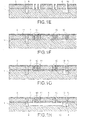
- FIGS. 1A to 1I illustrate the main steps of an implementation of the manufacturing method according to the present invention. These figures are cross-sectional views.
- reference numeral 1 denotes a solid monocrystalline silicon substrate. From the upper face 2 of the substrate 1, trenches 3 are made to receive the anchoring zones for electrically isolating and / or delimiting the mechanical component to be produced.
- the trenches 3 are then plugged by deposition of an anchoring material (for example SiN, SiO 2 , ...) followed by chemical mechanical polishing (or CMP) with a stop on the face 2 of the substrate 1.
- an anchoring material for example SiN, SiO 2 , ...) followed by chemical mechanical polishing (or CMP) with a stop on the face 2 of the substrate 1.
- CMP chemical mechanical polishing
- the epitaxy of a monocrystalline layer is carried out, for example a layer 5 of SiGe 50 nm thick to obtain the lower protective layer (see FIG. figure 1C ). Since the substrate 1 is monocrystalline, the epitaxial layer 5 is also monocrystalline. On the other hand, on the anchors 4, the epitaxial zones 6 are of polycrystalline SiGe.
- An epitaxy of a silicon layer is then carried out on layer 5 and zones 6.
- a layer of monocrystalline silicon 7 is obtained on layer 5.
- zones 8 of polycrystalline silicon see figure 1D ).
- the upper protective layer or stop layer 9 on the previously obtained structure is selective with respect to the release etching of the mechanical component, that is to say with respect to the monocrystalline silicon of the substrate, and preferably with respect to the lower protective layer 5. example a layer of SiO 2 .
- DRIE litho-etching is then performed on the upper protective layer 9, the silicon layer 7 and the lower protective layer 5. between the anchoring zones, according to a pattern of definition of the mechanical component, until reaching and revealing the silicon substrate 1 and to provide access routes 10 to this substrate.
- this protective layer 11 covers the upper protective layer 9, the walls of the access channels 10 and the bottom of the access channels, that is to say the silicon substrate 1 previously revealed . This is what the figure 1F .
- the protective layer 11 is then etched anisotropically with a stop on the upper protective layer 9. This etching makes it possible to keep the protective layer 11 only on the walls of the access paths 10, the silicon of the substrate 1 being new revealed (see the figure 1G ).
- the etched thickness of the substrate 1 may be between a few hundred nm and a few ⁇ m.
- the upper protective layer or barrier layer 9 and the protective layer of the 11. The result obtained is shown on the figure 1I .
- the lower protective layer 5 can also be removed by selective etching.
- the anchors in the silicon can be used to electrically isolate the MEMS / NEMS structure once released, but they can also serve as an etch stop at the release step. In the case where the electrical insulation is not necessary, these anchors can possibly be conductors or semiconductors and simply play this role of etching stop. Of course, this assumes that the material of these anchors does not become serious during this release step. Those skilled in the art will know which material to use.
- Additional steps can be interposed in this method, such as a metallization of the structure for the contact recovery before the etching of the MEMS, or a deposit and a planarization of the MEMS once released to continue other steps in the end process.
- the materials and additional steps will of course have to be compatible with the complete method described above. Nevertheless, those skilled in the art will be able to determine them.
- FIGS. 2A to 2C illustrate an addition of steps for producing contact pads.
- the same elements as on the Figures 1A to 1I are referenced identically.
- the upper protective layer or barrier layer 9 and the DRIE litho-etching of the upper protective layer 9, of the silicon layer 7 and of the lower protective layer 5 are then deposited until they are deposited. reaching and revealing the silicon substrate 1 and providing the access routes to the substrate. This is what the Figure 2B .
- the Figure 2C represents the structure obtained at the end of the process according to the invention.
- FIGS. 3A and 3B illustrate an implementation of the manufacturing method according to the present invention, allowing the manufacture of a stack of mechanical components.
- This stack is obtained by alternating protective layer 5 made of monocrystalline material other than silicon (and allowing epitaxy of monocrystalline silicon), for example SiGe and epitaxial monocrystalline silicon layer 7 on substrate 1 provided with its anchors 4 (see FIG. figure 3A ).
- the different epitaxies also alternate the epitaxial zones 6 in polycrystalline SiGe and 8 in polycrystalline silicon.
- the invention provides a number of advantages. It enables low cost technological stacking based on conventional microelectronics technological steps and using a standard substrate.
- the method of the invention may be CMOS compatible. It provides a recess that can be electrically insulating and thus do not require to isolate the MEMS or NEMS by additional dielectric and metal deposits as implemented in the SCREAM technique.
- the silicon protection layer is SiGe
- the etching of the silicon can be very selective with respect to the latter. We can therefore release large patterns, which gives flexibility as to the patterns that can be achieved by this technology.
- the anchors, electrically insulating or not, made in silicon can serve as an etch stop during the release step.
- the shape of the structures released is no longer limited by the isotropic nature of the release engraving, d where for example the possibility of making square and hexagonal suspended membranes, and no longer just circular.
Abstract
Description
L'invention se rapporte à un procédé de fabrication de composants mécaniques de structures MEMS (pour "Micro-Electro-Mechanical System") ou NEMS (pour "Nano-Electro-Mechanical System") en silicium monocristallin. Ces structures sont notamment utilisées pour la réalisation de capteurs et d'actionneurs.The invention relates to a method for manufacturing mechanical components of MEMS structures (for "Micro-Electro-Mechanical System") or NEMS (for "Nano-Electro-Mechanical System") monocrystalline silicon. These structures are used in particular for producing sensors and actuators.
L'utilisation du silicium monocristallin pour la réalisation de composants MEMS ou NEMS est intéressante à plusieurs titres. Ses propriétés mécaniques sont excellentes, notamment par rapport au silicium polycristallin. De fortes épaisseurs peuvent être utilisées (dans le cas du silicium polycristallin, l'épaisseur est généralement limitée à 20 µm). Il possède de très bonnes propriétés piézoélectriques. Ses propriétés semiconductrices, bien connues et bien maîtrisées, permettent une co-intégration de ces composants mécaniques avec l'électronique associée.The use of monocrystalline silicon for the production of MEMS or NEMS components is interesting for several reasons. Its mechanical properties are excellent, especially with respect to polycrystalline silicon. Large thicknesses can be used (in the case of polycrystalline silicon, the thickness is generally limited to 20 microns). It has very good piezoelectric properties. Its semiconducting properties, well known and well controlled, allow co-integration of these mechanical components with the associated electronics.
Dans l'état de l'art, on trouve trois grands modes de réalisation de structures MEMS/NEMS en silicium monocristallin, c'est-à-dire des composants mécaniques libérés, à même de pouvoir se déplacer sous l'action d'une force extérieure, en technologie de surface.In the state of the art, there are three major embodiments of MEMS / NEMS monocrystalline silicon structures, that is to say, mechanical components released, able to move under the action of a external force, in surface technology.
La technologie SOI est la plus répandue. Dans ce cas, le composant est réalisé sur la couche active du substrat SOI et l'oxyde enterré sert à la fois de couche d'arrêt de gravure du silicium et de couche sacrificielle. La libération de la structure mécanique se fait par la face avant du substrat. Une première variante consiste à graver toute la face arrière pour libérer le composant mécanique, en s'arrêtant sur l'oxyde enterré. La libération se fait alors par la face arrière du substrat. Une deuxième variante consiste à reporter le substrat SOI sur une cavité pour le libérer par simple gravure du silicium.SOI technology is the most widespread. In this case, the component is made on the active layer of the SOI substrate and the buried oxide serves as both a silicon etch stop layer and a sacrificial layer. The release of the mechanical structure is by the front face of the substrate. A first variant consists in engraving the entire rear face to release the mechanical component, stopping on the buried oxide. The release is then through the back side of the substrate. A second variant is to transfer the SOI substrate to a cavity to release it by simply etching the silicon.
L'intérêt de la technologie SOI pour les MEMS repose sur l'oxyde enterré que permet à la fois :
- de servir de couche d'arrêt à la gravure du silicium, et donc de définir avec précision l'épaisseur de la couche de silicium sur laquelle sera faite le composant (quelle que soit la variante),
- de servir de couche sacrificielle (dans le cas d'un procédé face avant principalement),
- d'avoir une couche isolante électrique soutenant le composant MEMS/NEMS (pour éviter de mettre tous les éléments du MEMS ou du NEMS en court-circuit).
- to serve as a stop layer for silicon etching, and therefore to precisely define the thickness of the silicon layer on which the component will be made (whatever the variant),
- to serve as a sacrificial layer (in the case of a front-end process mainly),
- to have an electrical insulating layer supporting the MEMS / NEMS component (to avoid putting all elements of MEMS or NEMS shorted).
Par contre, le gros inconvénient de la technologie SOI est son prix élevé. On a également observé récemment des problèmes de contraintes mal contrôlées dans le SOI qui, dans certaines configurations, sont très dommageables pour les MEMS/NEMS.On the other hand, the big disadvantage of the SOI technology is its high price. There have also been recently observed problems of poorly controlled constraints in the SOI which, in some configurations, are very damaging to MEMS / NEMS.
Dans la technologie SON (pour "Silicon-on-Nothing"), on fait croître une couche de SiGe sur un substrat de silicium standard, et sur cette couche de SiGe, on fait croître une couche de silicium monocristallin. Le composant MEMS/NEMS est réalisé sur cette dernière couche de silicium et le SiGe sert de couche sacrificielle. Pour la libération, on utilise une gravure sèche du SiGe à base de CF4, sélective par rapport au silicium monocristallin.In SON (for "Silicon-on-Nothing") technology, a layer of SiGe on a standard silicon substrate, and on this SiGe layer, a monocrystalline silicon layer is grown. The MEMS / NEMS component is made on this last silicon layer and the SiGe serves as a sacrificial layer. For the release, a dry etching of SiGe based on CF 4 , selective with respect to monocrystalline silicon, is used.
L'intérêt principal de la technologie SON, c'est qu'il s'agit d'un procédé bas coût. Cela permet également d'avoir accès à des épaisseurs de silicium très faibles (typiquement quelques 100 nm), par exemple pour les NEMS. Ses inconvénients sont par contre multiples.The main interest of SON technology is that it is a low cost process. This also makes it possible to have access to very low silicon thicknesses (typically some 100 nm), for example for NEMS. However, its disadvantages are multiple.
La gravure isotrope du SiGe est assez faiblement sélective par rapport au silicium. On est donc limité à des libérations de motifs étroits (typiquement inférieurs au µm). L'épaisseur de silicium épitaxié sur le SiGe est généralement limitée à quelques centaines de nanomètres (des dislocations risquent d'apparaître si l'on souhaite obtenir de fortes épaisseurs de silicium). Le SiGe est semiconducteur. Pour avoir des zones isolées électriquement sur le MEMS/NEMS, cela suppose de mettre une couche isolante dans les zones devant être isolées électriquement (dépôt SiO2 ou SiN par exemple). La couche de silicium épitaxiée au-dessus de cette couche isolante sera polycristalline (et non monocristalline). Ce point peut être assez critique puisque ces zones correspondent à des zones d'ancrage où le matériau est particulièrement sollicité. Le fait d'avoir un matériau polycristallin dans ces zones d'ancrage (plutôt que monocristallin) conduit soit à avoir un moins bon facteur de qualité, dans le cas de structures résonantes, soit à être plus sensible à des contraintes mécaniques (par exemple la tenue aux chocs).The isotropic etching of SiGe is rather weakly selective with respect to silicon. We are therefore limited to narrow pattern releases (typically less than 1 μm). The thickness of epitaxial silicon on the SiGe is generally limited to a few hundred nanometers (dislocations may occur if one wishes to obtain high thicknesses of silicon). SiGe is semiconductor. To have areas electrically insulated on the MEMS / NEMS, this involves putting an insulating layer in areas to be electrically isolated (SiO 2 or SiN deposit for example). The silicon layer epitaxied above this insulating layer will be polycrystalline (and not monocrystalline). This point can be quite critical since these zones correspond to anchoring zones where the material is particularly stressed. Having a polycrystalline material in these anchor zones (rather than monocrystalline) leads either to have a lower quality factor, in the case of resonant structures, or to be more sensitive to mechanical stresses (for example impact resistance).
Dans la technologie SCREAM, on part d'un substrat standard pour réaliser un composant MEMS et on utilise une partie "enterrée" du silicium massif comme couche sacrificielle. Le procédé se décompose de la manière suivante : gravure DRIE (pour "Deep Reactive Ion Etching" ou gravure ionique réactive profonde) de la structure MEMS, oxydation thermique, gravure anisotrope de l'oxyde, gravure isotrope du silicium pour libérer le MEMS, métallisation de la structure (sur les flancs et le dessus).In SCREAM technology, a standard substrate is used to make a MEMS component and a "buried" part of solid silicon is used as the sacrificial layer. The process is decomposed in the following way: DRIE (deep Reactive Ion Etching) etching of the MEMS structure, thermal oxidation, anisotropic etching of the oxide, isotropic etching of the silicon to release the MEMS, metallization of the structure (on the flanks and on the top).
L'intérêt principal de la technologie SCREAM, c'est sa simplicité et son aspect bas coût.The main interest of SCREAM technology is its simplicity and its low cost aspect.
Ses inconvénients sont par contre multiples. Il n'y a pas d'ancrage isolant. Cela se solde par la création de contraintes mécaniques importantes sur le MEMS (dus à la présence de l'oxyde thermique et du métal sur les structures libérées). Cet ajout d'oxyde et de métal sur le silicium monocristallin rend le composant mécanique moins bon (moins bon facteur de qualité dans le cas d'un résonateur par exemple). La métallisation, qui se fait après libération de la structure, nécessite l'utilisation d'un masquage mécanique lors du dépôt. Cette méthode est peu industrielle et donne une résolution des motifs très médiocre.However, its disadvantages are multiple. There is no insulating anchor. This results in the creation of significant mechanical stresses on the MEMS (due to the presence of thermal oxide and metal on the structures released). This addition of oxide and metal on the monocrystalline silicon makes the mechanical component less good (less good quality factor in the case of a resonator for example). The metallization, which is done after release of the structure, requires the use of a mechanical masking during the deposition. This method is not very industrial and gives a very poor pattern resolution.
La technologie SCREAM procure des structures mal définies et qui se gravent sous le masque d'oxyde lors de la gravure isotrope du silicium (absence d'oxyde sous la structure à libérer).SCREAM technology provides poorly defined structures that burn under the oxide mask during the isotropic etching of silicon (absence of oxide under the structure to be released).
La présente invention a été conçue pour remédier aux inconvénients des procédés de l'art antérieur décrits ci-dessus.The present invention has been designed to overcome the disadvantages of the methods of the prior art described above.
Le procédé selon l'invention peut être utilisé pour toutes les applications MEMS et NEMS. Il met en oeuvre une technologie adaptée aux marchés bas coût et grands volumes : téléphonie mobile, automobile, jeux,.... A titre d'exemple, on peut citer :
- pour les automobiles : les accéléromètres, les gyromètres, les capteurs de pression, les capteurs chimiques à base de résonateurs mécaniques MEMS ou NEMS,
- pour la téléphonie mobile : les bases de temps (résonateurs RF), les filtres mécaniques MEMS ou NEMS, les accéléromètres, les microphones,
- pour les jeux : les accéléromètres, les gyromètres.
- for automobiles: accelerometers, gyrometers, pressure sensors, chemical sensors based on MEMS or NEMS mechanical resonators,
- for mobile telephony: time bases (RF resonators), MEMS or NEMS mechanical filters, accelerometers, microphones,
- for games: accelerometers, gyrometers.
L'invention a pour objet un procédé de fabrication d'au moins un composant mécanique de structure MEMS ou NEMS à partir d'un substrat de silicium monocristallin, comprenant les étapes de :
- a) formation de zones d'ancrage dans une face du substrat pour délimiter au moins en partie le composant mécanique,
- b) formation, sur ladite face du substrat, d'une couche de protection inférieure en matériau autre que le silicium et obtenue par épitaxie à partir de ladite face du substrat, cette couche de protection inférieure étant monocristalline au moins en dehors des zones d'ancrage,
- c) formation sur la couche de protection inférieure d'une couche de silicium obtenue par épitaxie à partir de la couche de protection inférieure, cette couche de silicium étant monocristalline au moins en dehors des zones d'ancrage,
- d) formation d'une couche de protection supérieure sur la couche de silicium,
- e) gravure de la couche de protection supérieure, de la couche de silicium et de la couche de protection inférieure, entre les zones d'ancrage, selon un motif de définition du composant mécanique, jusqu'à atteindre le substrat de silicium monocristallin et fournir des voies d'accès au substrat de silicium monocristallin,
- f) formation d'une couche de protection sur les parois formées par la gravure du motif du composant mécanique dans la couche de silicium épitaxiée,
- g) libération du composant mécanique par gravure isotrope du substrat de silicium monocristallin à partir des voies d'accès au substrat de silicium monocristallin, cette gravure isotrope n'attaquant pas les couches de protection inférieure et supérieure et la couche de protection des parois.
- a) formation of anchoring zones in a face of the substrate to delimit at least part of the mechanical component,
- b) forming, on said substrate side, a lower protective layer of material other than silicon and obtained by epitaxy from said substrate face, this lower protective layer being monocrystalline at least outside the anchoring zones,
- c) formation on the lower protective layer of a silicon layer obtained by epitaxy from the lower protective layer, this silicon layer being monocrystalline at least outside the anchoring zones,
- d) forming an upper protective layer on the silicon layer,
- e) etching the upper protection layer, the silicon layer and the lower protective layer, between the anchoring zones, according to a definition pattern of the mechanical component, until reaching the single-crystal silicon substrate and providing access paths to the monocrystalline silicon substrate,
- f) forming a protective layer on the walls formed by the etching of the mechanical component pattern in the epitaxial silicon layer,
- g) release of the mechanical component by isotropic etching of the monocrystalline silicon substrate from the access paths to the monocrystalline silicon substrate, this isotropic etching not attacking the lower and upper protection layers and the protective layer of the walls.
Avantageusement, les zones d'ancrage peuvent permettre d'isoler électriquement le composant mécanique du reste du substrat. Ces zones d'ancrage sont alors en matériau diélectrique.Advantageously, the anchoring zones can make it possible to isolate the mechanical component electrically from the rest of the substrate. These anchoring zones are then made of dielectric material.
Lors de l'étape e), la couche de protection supérieure, la couche de silicium et la couche de protection inférieure peuvent être également gravées dans les zones d'ancrage selon un motif apte à créer une zone d'isolation électrique dans les couches épitaxiées.During step e), the upper protective layer, the silicon layer and the lower protective layer may also be etched in the anchoring zones in a pattern capable of creating an electrical insulation zone in the epitaxial layers. .
Selon un mode de réalisation particulier, avant l'étape e), il est prévu une étape de réalisation de plots de contact électrique pour le composant mécanique. Cette réalisation peut comprendre le dépôt d'une couche de matériau électriquement conducteur (par exemple en Al ou en AlSi) et sa gravure. Les plots de contact électrique peuvent être disposés sur les zones d'ancrage.According to a particular embodiment, before step e), there is provided a step of producing electrical contact pads for the mechanical component. This embodiment may comprise the deposition of a layer of electrically conductive material (for example Al or AlSi) and its etching. The electrical contact pads can be arranged on the anchoring zones.
Selon un mode de mise en oeuvre particulier, le composant mécanique est fabriqué en intercalant entre les étapes c) et d) au moins les deux étapes suivantes :
- formation, sur la structure obtenue à l'étape c), d'une couche intermédiaire en matériau autre que le silicium et obtenue par épitaxie à partir de la couche de silicium déposée juste précédemment, cette couche intermédiaire étant monocristalline au moins en dehors des zones d'ancrage,
- formation sur la couche intermédiaire déposée juste précédemment d'une couche de silicium obtenue par épitaxie à partir de cette couche intermédiaire, cette couche de silicium étant monocristalline au moins en dehors des zones d'ancrage.
- forming, on the structure obtained in step c), an intermediate layer of material other than silicon and obtained by epitaxy from the silicon layer deposited just above, this intermediate layer being monocrystalline at least outside the zones anchoring,
- formation on the intermediate layer deposited just previously of a silicon layer obtained by epitaxy from this intermediate layer, this silicon layer being monocrystalline at least outside the anchoring zones.
Les zones d'ancrage peuvent être formées en réalisant des tranchées dans ladite face du substrat et en remplissant ces tranchées par un matériau d'ancrage. Le matériau d'ancrage peut être un matériau permettant successivement la formation d'une couche épitaxiée simultanément à la couche de protection inférieure et la formation d'une autre couche épitaxiée simultanément à la couche de silicium.The anchoring zones may be formed by making trenches in said face of the substrate and filling these trenches with anchoring material. The anchoring material may be a material that successively allows the formation of an epitaxial layer simultaneously with the lower protective layer and the formation of another epitaxial layer simultaneously with the silicon layer.
La couche de protection des parois peut être formée par dépôt ou épitaxie d'une couche de protection épousant le relief de la structure gravée à l'étape e), puis par gravure anisotrope de cette couche de protection.The protective layer of the walls may be formed by deposition or epitaxy of a protective layer conforming to the relief of the structure etched in step e), then by anisotropic etching of this protective layer.
A titre d'exemple, les zones d'ancrage formées dans la face du substrat sont en nitrure de silicium ou en oxyde de silicium, la couche de protection en matériau autre que le silicium est du SiGe, la couche de protection supérieure est en nitrure de silicium ou en oxyde de silicium et la couche de protection sur les parois est en un matériau choisi parmi SiGe, l'oxyde de silicium et le nitrure de silicium.By way of example, the anchoring zones formed in the face of the substrate are made of silicon nitride or silicon oxide, the protective layer of material other than silicon is SiGe, the upper protective layer is made of nitride. of silicon or silicon oxide and the protective layer on the walls is of a material selected from SiGe, silicon oxide and silicon nitride.
L'invention sera mieux comprise et d'autres avantages et particularités apparaîtront à la lecture de la description qui va suivre, donnée à titre d'exemple non limitatif, accompagnée des dessins annexés parmi lesquels :
- les
figures 1A à 1I illustrent une mise en oeuvre du procédé de fabrication selon la présente invention, - les
figures 2A à 2C illustrent des étapes supplémentaires du procédé de fabrication selon la présente invention, - les
figures 3A et 3B illustrent une mise en oeuvre du procédé de fabrication selon la présente invention, permettant la fabrication d'un empilement de composants mécaniques.
- the
Figures 1A to 1I illustrate an implementation of the manufacturing method according to the present invention, - the
FIGS. 2A to 2C illustrate additional steps of the manufacturing method according to the present invention, - the
Figures 3A and 3B illustrate an implementation of the manufacturing method according to the present invention, allowing the manufacture of a stack of mechanical components.
Selon la présente invention, il est proposé d'utiliser un empilement de couches permettant la réalisation de structures MEMS ou NEMS en silicium monocristallin, réalisées sur la base de technologies planaires, compatibles CMOS, qui n'utilisent pas de substrat SOI. L'objectif étant d'avoir un procédé bas coût, compatible CMOS et permettant d'adresser un large éventail de motifs de MEMS et NEMS en silicium monocristallin (c'est-à-dire faiblement dépendant des règles de dessin).According to the present invention, it is proposed to use a stack of layers allowing the realization of MEMS or NEMS monocrystalline silicon structures, made on the basis of planar technologies, CMOS compatible, which do not use SOI substrate. The goal is to have a low cost, CMOS-compatible process for addressing a wide range of MEMS and NEMS patterns in monocrystalline silicon (i.e., weakly dependent on the drawing rules).
Pour cela, le silicium massif est utilisé pour fournir la couche sacrificielle de la structure MEMS/NEMS. Il est prévu des ancrages, éventuellement en matériau électriquement isolant, formant zones d'arrêt à la gravure servant à la libération des composants mécaniques. Le composant MEMS ou NEMS est réalisé à partir d'une couche de silicium monocristallin épitaxiée. Le composant MEMS ou NEMS usiné est entièrement protégé avant l'étape de libération par des couches résistant à la chimie de gravure de libération. Ces couches comprennent une couche de protection inférieure (protégeant le composant mécanique par le dessous), une couche de protection supérieure (protégeant le composant mécanique par le dessus) et une couche de protection des parois formées par la gravure du motif du composant mécanique.For this, solid silicon is used to provide the sacrificial layer of the MEMS / NEMS structure. Anchors are provided, possibly of electrically insulating material, forming etching stop zones for the release of the mechanical components. The MEMS or NEMS component is made from an epitaxial monocrystalline silicon layer. The machined MEMS or NEMS component is fully protected prior to the release step by release etch chemistry resistant layers. These layers include a protective layer lower (protecting the mechanical component from below), an upper protective layer (protecting the mechanical component from above) and a protective layer of the walls formed by the etching of the mechanical component pattern.
La couche de protection inférieure est en matériau monocristallin, autre que le silicium, et est épitaxiée à partir du substrat en silicium monocristallin. Elle présente les caractéristiques suivantes. Elle permet une recroissance de silicium monocristallin par épitaxie, avec éventuellement une possibilité de dopage in situ du silicium ainsi épitaxié. Elle résiste à une gravure sèche ou humide du silicium (gravure sélective) sans être attaquée ou en étant faiblement attaquée. Eventuellement, elle peut être gravée sélectivement par rapport au silicium par un procédé de gravure sèche ou humide.The lower protective layer is made of monocrystalline material, other than silicon, and is epitaxially grown from the monocrystalline silicon substrate. It has the following characteristics. It allows re-growth of monocrystalline silicon by epitaxy, possibly with a possibility of doping in situ of the silicon thus epitaxially grown. It resists dry or wet etching of silicon (selective etching) without being attacked or weakly attacked. Optionally, it can be etched selectively with respect to silicon by a dry or wet etching process.
La couche de protection supérieure et la couche de protection des parois du composant à libérer présentent les caractéristiques suivantes.The upper protective layer and the protective layer of the walls of the component to be released have the following characteristics.
Elles peuvent résister à une gravure sèche ou humide du silicium (gravure sélective) sans être attaquées, ou en étant faiblement attaquées. Eventuellement, elles peuvent être gravées sélectivement par rapport au silicium par un procédé de gravure sèche ou humide. Préférentiellement, la couche de protection du dessus (ou couche d'arrêt dans la description de l'empilement) est sélective à la gravure de la couche de protection des parois (c'est-à-dire qu'elle ne se grave pas ou se grave peu, lors de l'étape de gravure de la couche de protection des parois).They can withstand a dry or wet etching of silicon (selective etching) without being attacked, or being weakly attacked. Optionally, they can be etched selectively with respect to silicon by a dry or wet etching process. Preferably, the top protection layer (or stop layer in the description of the stack) is selective for etching the protective layer of the walls (that is to say, it does not get damaged or gets serious little, when the step of etching the protective layer of the walls).
La couche de protection du dessous peut par exemple être du SiGe monocristallin. La couche de protection des parois peut par exemple être du SiGe (monocristallin ou polycristallin), du SiO2, du SiN,.... Cette couche devra être conforme (pour bien recouvrir les parois). La couche de protection sur le dessus (couche d'arrêt) peut par exemple être du SiO2, du SiN,....The protective layer of the underside may for example be monocrystalline SiGe. The protective layer of the walls may for example be SiGe (monocrystalline or polycrystalline), SiO 2 , SiN, .... This layer must be consistent (to cover the walls). The protective layer on the top (stop layer) may for example be SiO 2 , SiN, ....
Des ancrages isolants électriquement (et/ou arrêt de gravure) pourront être réalisés, avant le dépôt de la couche de protection inférieure, en gravant le silicium massif, puis en comblant les cavités ainsi réalisées par dépôt d'un matériau isolant (par exemple SiO2 ou SiN) et en retirant l'excédent par planarisation CMP ou par l'enchaînement litho-gravure et CMP. Dans le cas où ces ancrages ne servent que d'arrêt de gravure, le matériau de remplissage des cavités pourra être isolant, conducteur ou semiconducteur.Electrically insulating anchors (and / or etching stop) may be made, before the deposition of the lower protective layer, by etching the solid silicon, and then filling the cavities thus produced by deposition of an insulating material (for example SiO 2 or SiN) and removing the surplus by CMP planarization or litho-etching and CMP. In the case where these anchors serve only to stop etching, the filling material of the cavities may be insulating, conductive or semiconductor.
Les
Sur la
Les tranchées 3 sont ensuite bouchées par dépôt d'un matériau d'ancrage (par exemple SiN, SiO2, ...) suivi d'un polissage mécano-chimique (ou CMP) avec arrêt sur la face 2 du substrat 1. Le résultat obtenu est montré sur la
On procède ensuite, sur la face 2 du substrat 1 à l'épitaxie d'une couche monocristalline, par exemple une couche 5 de SiGe d'épaisseur 50 nm pour obtenir la couche de protection inférieure (voir la
On procède ensuite à l'épitaxie d'une couche de silicium, de quelques dizaines de nm à quelques µm d'épaisseur, sur la couche 5 et les zones 6. On obtient, sur la couche 5, une couche de silicium monocristallin 7 et, sur les zones 6, des zones 8 de silicium polycristallin (voir la
On dépose ensuite, comme le montre la
Ensuite, on forme par dépôt ou par épitaxie une couche de protection des parois formées par la gravure du motif du composant mécanique. Lorsqu'elle est formée, cette couche de protection 11 recouvre la couche de protection supérieure 9, les parois des voies d'accès 10 et le fond des voies d'accès, c'est-à-dire le substrat de silicium 1 précédemment révélé. C'est ce que montre la
La couche de protection 11 est ensuite gravée de manière anisotrope avec arrêt sur la couche de protection supérieure 9. Cette gravure permet de ne conserver la couche de protection 11 que sur les parois des voies d'accès 10, le silicium du substrat 1 étant à nouveau révélé (voir la
On peut alors procéder à la gravure isotrope du silicium du substrat 1, entre les ancrages 4. Cette gravure est sélective par rapport aux couches de protection 5, 9 et 11. Le silicium du composant mécanique, c'est-à-dire le matériau de la couche 7, demeure intact. On obtient une cavité 12 sous le composant mécanique ainsi libéré (voir la
On peut alors procéder à l'élimination, par gravure sélective par rapport au silicium monocristallin, de la couche de protection supérieure ou couche d'arrêt 9 et de la couche de protection des parois 11. Le résultat obtenu est montré sur la
Les ancrages dans le silicium peuvent servir à isoler électriquement la structure MEMS/NEMS une fois libérée, mais ils peuvent servir également d'arrêt de gravure à l'étape de libération. Dans le cas où l'isolation électrique n'est pas nécessaire, ces ancrages peuvent éventuellement être conducteurs ou semiconducteurs et jouer simplement ce rôle d'arrêt de gravure. Bien évidemment, cela suppose que le matériau de ces ancrages ne se grave pas lors de cette étape de libération. L'homme de l'art saura quel matériau utiliser.The anchors in the silicon can be used to electrically isolate the MEMS / NEMS structure once released, but they can also serve as an etch stop at the release step. In the case where the electrical insulation is not necessary, these anchors can possibly be conductors or semiconductors and simply play this role of etching stop. Of course, this assumes that the material of these anchors does not become serious during this release step. Those skilled in the art will know which material to use.
Des étapes supplémentaires peuvent venir s'intercaler dans ce procédé, comme par exemple une métallisation de la structure pour la reprise de contact avant la gravure du MEMS, ou un dépôt et une planarisation du MEMS une fois libéré pour continuer d'autres étapes en fin de procédé. Les matériaux et étapes additionnels devront bien évidemment être compatibles avec le procédé complet décrit précédemment. Néanmoins, l'homme de l'art sera en mesure de les déterminer.Additional steps can be interposed in this method, such as a metallization of the structure for the contact recovery before the etching of the MEMS, or a deposit and a planarization of the MEMS once released to continue other steps in the end process. The materials and additional steps will of course have to be compatible with the complete method described above. Nevertheless, those skilled in the art will be able to determine them.
A titre d'exemple, les
Après l'étape d'épitaxie de silicium, fournissant la couche de silicium monocristallin 7 et les zones 8 de silicium polycristallin, on forme des plots de contact électrique sur les zones 8. Ces plots de contact sont formés par dépôt d'une couche métallique et litho-gravure. La
On procède ensuite au dépôt de la couche de protection supérieure ou couche d'arrêt 9 et à la litho-gravure DRIE de la couche de protection supérieure 9, de la couche de silicium 7 et de la couche de protection inférieure 5, jusqu'à atteindre et révéler le substrat en silicium 1 et pour fournir les voies d'accès 10 au substrat. C'est ce que montre la
La
Les
Cet empilement est obtenu en alternant couche de protection 5 en matériau monocristallin autre que le silicium (et permettant une épitaxie de silicium monocristallin), par exemple SiGe et couche de silicium monocristallin épitaxiée 7 sur le substrat 1 pourvu de ses ancrages 4 (voir la
Les étapes suivantes sont identiques aux étapes correspondantes déjà décrites. Après l'étape de libération et l'élimination de la couche d'arrêt supérieure et de la couche de protection des parois, on obtient la structure représentée à la
L'invention procure un certain nombre d'avantages. Elle permet un empilement technologique bas coût reposant sur des étapes technologiques classiques de la microélectronique et utilisant un substrat standard. Le procédé de l'invention peut être compatible CMOS. Il procure un encastrement pouvant être électriquement isolant et ainsi ne pas nécessiter d'isoler le MEMS ou le NEMS par des dépôts diélectrique et métallique supplémentaires tels que mis en oeuvre dans la technique SCREAM. Dans le cas où la couche de protection du silicium est du SiGe, la gravure du silicium peut être très sélective par rapport à cette dernière. On peut donc libérer de grands motifs, ce qui donne de la souplesse quant aux motifs que l'on peut réaliser par cette technologie. Les ancrages, électriquement isolants ou non, réalisés dans le silicium peuvent servir d'arrêt de gravure lors de l'étape de libération. Il en résulte un meilleur contrôle de l'étape de libération (pas de risque de surgravure par exemple) et un accès à des motifs variés : la forme des structures libérées n'est plus limitée par la nature isotrope de la gravure de libération, d'où par exemple la possibilité de réaliser des membranes suspendues carrées et hexagonales, et non plus seulement circulaires.The invention provides a number of advantages. It enables low cost technological stacking based on conventional microelectronics technological steps and using a standard substrate. The method of the invention may be CMOS compatible. It provides a recess that can be electrically insulating and thus do not require to isolate the MEMS or NEMS by additional dielectric and metal deposits as implemented in the SCREAM technique. In the case where the silicon protection layer is SiGe, the etching of the silicon can be very selective with respect to the latter. We can therefore release large patterns, which gives flexibility as to the patterns that can be achieved by this technology. The anchors, electrically insulating or not, made in silicon can serve as an etch stop during the release step. This results in better control of the release step (no risk of overgrafting for example) and access to various patterns: the shape of the structures released is no longer limited by the isotropic nature of the release engraving, d where for example the possibility of making square and hexagonal suspended membranes, and no longer just circular.
Claims (16)
Applications Claiming Priority (1)
| Application Number | Priority Date | Filing Date | Title |
|---|---|---|---|
| FR0760426A FR2925890B1 (en) | 2007-12-28 | 2007-12-28 | METHOD FOR MANUFACTURING MECHANICAL COMPONENTS OF MONOCRYSTALLINE SILICON MEMS OR NEMS STRUCTURES |
Publications (2)
| Publication Number | Publication Date |
|---|---|
| EP2075222A1 true EP2075222A1 (en) | 2009-07-01 |
| EP2075222B1 EP2075222B1 (en) | 2010-07-07 |
Family
ID=39769267
Family Applications (1)
| Application Number | Title | Priority Date | Filing Date |
|---|---|---|---|
| EP08172514A Active EP2075222B1 (en) | 2007-12-28 | 2008-12-22 | Herstellungsverfahren von mechanischen Komponenten von MEMS- oder NEMS-Strukturen aus monokristallinem Silizium |
Country Status (6)
| Country | Link |
|---|---|
| US (1) | US7932118B2 (en) |
| EP (1) | EP2075222B1 (en) |
| JP (1) | JP2009160728A (en) |
| AT (1) | ATE473199T1 (en) |
| DE (1) | DE602008001711D1 (en) |
| FR (1) | FR2925890B1 (en) |
Cited By (5)
| Publication number | Priority date | Publication date | Assignee | Title |
|---|---|---|---|---|
| CN101993033B (en) * | 2009-08-19 | 2012-05-23 | 微智半导体股份有限公司 | Micro electro mechanical system structure and manufacturing method |
| EP3088969A1 (en) * | 2016-03-17 | 2016-11-02 | Sigatec SA | Thermocompensated hairspring and method of production thereof |
| EP3285124A1 (en) * | 2016-08-17 | 2018-02-21 | Richemont International SA | Mechanical resonator for timepiece and method for manufacturing such a resonator |
| DE102018214634B3 (en) | 2018-08-29 | 2019-09-12 | Robert Bosch Gmbh | Sensor device and method for producing a sensor device |
| CN115966865A (en) * | 2022-12-29 | 2023-04-14 | 中国电子科技集团公司第二十六研究所 | MEMS filter generating out-of-band zero point based on three-dimensional stacking and manufacturing method thereof |
Families Citing this family (8)
| Publication number | Priority date | Publication date | Assignee | Title |
|---|---|---|---|---|
| US8945970B2 (en) * | 2006-09-22 | 2015-02-03 | Carnegie Mellon University | Assembling and applying nano-electro-mechanical systems |
| TWI373450B (en) | 2009-07-29 | 2012-10-01 | Pixart Imaging Inc | Microelectronic device and method for fabricating mems resonator thereof |
| US8603848B2 (en) * | 2009-08-25 | 2013-12-10 | Electronics And Telecommunications Research Institute | Three-dimensional MEMS structure and method of manufacturing the same |
| US8642370B2 (en) * | 2011-03-04 | 2014-02-04 | Texas Instruments Incorporated | Cavity open process to improve undercut |
| CN102584331B (en) * | 2012-01-18 | 2013-10-30 | 广西大学 | Method for preparing double-component and double-layer nano lubrication thin film by taking nano-particle array as template |
| US10246325B2 (en) * | 2014-09-03 | 2019-04-02 | Infineon Technologies Ag | MEMS device and method for manufacturing a MEMS device |
| US9630836B2 (en) * | 2015-09-30 | 2017-04-25 | Mems Drive, Inc. | Simplified MEMS device fabrication process |
| US20220415703A1 (en) * | 2021-06-24 | 2022-12-29 | Stmicroelectronics S.R.L. | Ultra-thin semiconductor die with irregular textured surfaces |
Citations (3)
| Publication number | Priority date | Publication date | Assignee | Title |
|---|---|---|---|---|
| US5198390A (en) * | 1992-01-16 | 1993-03-30 | Cornell Research Foundation, Inc. | RIE process for fabricating submicron, silicon electromechanical structures |
| DE10235371A1 (en) * | 2002-08-02 | 2004-02-12 | Robert Bosch Gmbh | Production of a micromechanical device used in integrated optical arrangements comprises preparing an SOI or EOI substrate having a silicon functional layer, forming a trench extending through the functional layer, and further processing |
| FR2857952A1 (en) * | 2003-07-25 | 2005-01-28 | St Microelectronics Sa | MEMS type electromechanical resonator, has vibrating beam anchored in shallow trench isolation region by one free end and comprising monocrystalline silicon median part |
Family Cites Families (3)
| Publication number | Priority date | Publication date | Assignee | Title |
|---|---|---|---|---|
| US6635506B2 (en) * | 2001-11-07 | 2003-10-21 | International Business Machines Corporation | Method of fabricating micro-electromechanical switches on CMOS compatible substrates |
| EP1521301A1 (en) * | 2003-09-30 | 2005-04-06 | Interuniversitaire Microelectronica Centrum vzw ( IMEC) | Method of formation of airgaps around interconnecting line |
| EP1544163B1 (en) * | 2003-12-16 | 2021-02-24 | Robert Bosch GmbH | Method for producing a membrane sensor and corresponding membrane sensor |
-
2007
- 2007-12-28 FR FR0760426A patent/FR2925890B1/en not_active Expired - Fee Related
-
2008
- 2008-12-17 US US12/336,930 patent/US7932118B2/en active Active
- 2008-12-22 JP JP2008325334A patent/JP2009160728A/en active Pending
- 2008-12-22 AT AT08172514T patent/ATE473199T1/en not_active IP Right Cessation
- 2008-12-22 EP EP08172514A patent/EP2075222B1/en active Active
- 2008-12-22 DE DE602008001711T patent/DE602008001711D1/en active Active
Patent Citations (3)
| Publication number | Priority date | Publication date | Assignee | Title |
|---|---|---|---|---|
| US5198390A (en) * | 1992-01-16 | 1993-03-30 | Cornell Research Foundation, Inc. | RIE process for fabricating submicron, silicon electromechanical structures |
| DE10235371A1 (en) * | 2002-08-02 | 2004-02-12 | Robert Bosch Gmbh | Production of a micromechanical device used in integrated optical arrangements comprises preparing an SOI or EOI substrate having a silicon functional layer, forming a trench extending through the functional layer, and further processing |
| FR2857952A1 (en) * | 2003-07-25 | 2005-01-28 | St Microelectronics Sa | MEMS type electromechanical resonator, has vibrating beam anchored in shallow trench isolation region by one free end and comprising monocrystalline silicon median part |
Cited By (6)
| Publication number | Priority date | Publication date | Assignee | Title |
|---|---|---|---|---|
| CN101993033B (en) * | 2009-08-19 | 2012-05-23 | 微智半导体股份有限公司 | Micro electro mechanical system structure and manufacturing method |
| EP3088969A1 (en) * | 2016-03-17 | 2016-11-02 | Sigatec SA | Thermocompensated hairspring and method of production thereof |
| EP3285124A1 (en) * | 2016-08-17 | 2018-02-21 | Richemont International SA | Mechanical resonator for timepiece and method for manufacturing such a resonator |
| DE102018214634B3 (en) | 2018-08-29 | 2019-09-12 | Robert Bosch Gmbh | Sensor device and method for producing a sensor device |
| JP7393155B2 (en) | 2018-08-29 | 2023-12-06 | ロベルト・ボッシュ・ゲゼルシャフト・ミト・ベシュレンクテル・ハフツング | Sensor device and method of manufacturing the sensor device |
| CN115966865A (en) * | 2022-12-29 | 2023-04-14 | 中国电子科技集团公司第二十六研究所 | MEMS filter generating out-of-band zero point based on three-dimensional stacking and manufacturing method thereof |
Also Published As
| Publication number | Publication date |
|---|---|
| US7932118B2 (en) | 2011-04-26 |
| EP2075222B1 (en) | 2010-07-07 |
| ATE473199T1 (en) | 2010-07-15 |
| US20090170231A1 (en) | 2009-07-02 |
| FR2925890B1 (en) | 2010-01-29 |
| DE602008001711D1 (en) | 2010-08-19 |
| JP2009160728A (en) | 2009-07-23 |
| FR2925890A1 (en) | 2009-07-03 |
Similar Documents
| Publication | Publication Date | Title |
|---|---|---|
| EP2075222B1 (en) | Herstellungsverfahren von mechanischen Komponenten von MEMS- oder NEMS-Strukturen aus monokristallinem Silizium | |
| EP2143684B1 (en) | Method of manufacturing a MEMS/NEMS structure comprising a partially monocrystalline anchor | |
| EP2138454B1 (en) | Method of manufacturing a device using a substrate having a monocrystalline silicon sacrificial layer. | |
| EP2138451B1 (en) | Method for manufacturing a MEMS/NEMS electromechanical component in a monocrystalline material | |
| EP2599746B1 (en) | Process for forming a structure having at least a multi-thickness active part | |
| EP2808297B1 (en) | Methof for forming a suspended portion of a microelectronic and/or nanoelectronic structure in a monolithic part of a substrate | |
| FR2818627A1 (en) | MICROMECHANICAL COMPONENT AND METHOD FOR MANUFACTURING SUCH A COMPONENT | |
| EP1834924A2 (en) | Packaging of a microelectronic component, in particular a MEMS, in an airtight cavity | |
| EP1905734B1 (en) | Method of manufacture of an electromechanical component on a planar substrate | |
| EP2952472B1 (en) | Improved method for the production of suspended elements with different thicknesses for mems and nems structure | |
| EP2599745B1 (en) | Fabrication of a MEMS device having moving parts of different thicknesses. | |
| EP2840589B1 (en) | Improved separation method between an active area of a substrate and the rear surface thereof or a portion of the rear surface thereof | |
| EP2364953B1 (en) | Fabrication process for a microelectromechanical system by etching a sacrificial layer through a porous region. | |
| FR2875947A1 (en) | Production of a new structure incorporating superficial , buried and support layers, for micro- electronic and micro-system applications | |
| EP2138455B1 (en) | Process for making a MEMS structure with a moving element using a heterogeneous sacrificial layer | |
| EP2776364A1 (en) | Improved process for producing a device comprising cavities formed between a suspended element resting on insulating pads semi-buried in a substrate and this substrate | |
| EP3900064B1 (en) | Method for transferring a surface layer to cavities | |
| FR2757941A1 (en) | METHOD FOR PRODUCING A SUSPENDED ELEMENT IN A MICRO-FACTORY STRUCTURE | |
| EP2138453B1 (en) | Method for manufacturing an electromechanical structure comprising at least one mechanical reinforcement post | |
| EP2862836B1 (en) | Method for electrochemically producing at least one porous region of a micro- and/or nanoelectronic structure | |
| EP4269331A1 (en) | Method of manufacturing a mems device | |
| EP4128330A1 (en) | Method for producing a stacked structure |
Legal Events
| Date | Code | Title | Description |
|---|---|---|---|
| PUAI | Public reference made under article 153(3) epc to a published international application that has entered the european phase |
Free format text: ORIGINAL CODE: 0009012 |
|
| AK | Designated contracting states |
Kind code of ref document: A1 Designated state(s): AT BE BG CH CY CZ DE DK EE ES FI FR GB GR HR HU IE IS IT LI LT LU LV MC MT NL NO PL PT RO SE SI SK TR |
|
| AX | Request for extension of the european patent |
Extension state: AL BA MK RS |
|
| 17P | Request for examination filed |
Effective date: 20091223 |
|
| GRAP | Despatch of communication of intention to grant a patent |
Free format text: ORIGINAL CODE: EPIDOSNIGR1 |
|
| AKX | Designation fees paid |
Designated state(s): AT BE BG CH CY CZ DE DK EE ES FI FR GB GR HR HU IE IS IT LI LT LU LV MC MT NL NO PL PT RO SE SI SK TR |
|
| RTI1 | Title (correction) |
Free format text: HERSTELLUNGSVERFAHREN VON MECHANISCHEN KOMPONENTEN VON MEMS- ODER NEMS-STRUKTUREN AUS MONOKRISTALLINEM SILIZIUM |
|
| RAP1 | Party data changed (applicant data changed or rights of an application transferred) |
Owner name: COMMISSARIAT A L'ENERGIE ATOMIQUE ET AUX ENERGIES |
|
| GRAS | Grant fee paid |
Free format text: ORIGINAL CODE: EPIDOSNIGR3 |
|
| GRAA | (expected) grant |
Free format text: ORIGINAL CODE: 0009210 |
|
| AK | Designated contracting states |
Kind code of ref document: B1 Designated state(s): AT BE BG CH CY CZ DE DK EE ES FI FR GB GR HR HU IE IS IT LI LT LU LV MC MT NL NO PL PT RO SE SI SK TR |
|
| REG | Reference to a national code |
Ref country code: GB Ref legal event code: FG4D Free format text: NOT ENGLISH |
|
| REG | Reference to a national code |
Ref country code: CH Ref legal event code: EP |
|
| REG | Reference to a national code |
Ref country code: IE Ref legal event code: FG4D |
|
| REF | Corresponds to: |
Ref document number: 602008001711 Country of ref document: DE Date of ref document: 20100819 Kind code of ref document: P |
|
| REG | Reference to a national code |
Ref country code: NL Ref legal event code: VDEP Effective date: 20100707 |
|
| PG25 | Lapsed in a contracting state [announced via postgrant information from national office to epo] |
Ref country code: SI Free format text: LAPSE BECAUSE OF FAILURE TO SUBMIT A TRANSLATION OF THE DESCRIPTION OR TO PAY THE FEE WITHIN THE PRESCRIBED TIME-LIMIT Effective date: 20100707 |
|
| LTIE | Lt: invalidation of european patent or patent extension |
Effective date: 20100707 |
|
| PG25 | Lapsed in a contracting state [announced via postgrant information from national office to epo] |
Ref country code: AT Free format text: LAPSE BECAUSE OF FAILURE TO SUBMIT A TRANSLATION OF THE DESCRIPTION OR TO PAY THE FEE WITHIN THE PRESCRIBED TIME-LIMIT Effective date: 20100707 Ref country code: FI Free format text: LAPSE BECAUSE OF FAILURE TO SUBMIT A TRANSLATION OF THE DESCRIPTION OR TO PAY THE FEE WITHIN THE PRESCRIBED TIME-LIMIT Effective date: 20100707 Ref country code: LT Free format text: LAPSE BECAUSE OF FAILURE TO SUBMIT A TRANSLATION OF THE DESCRIPTION OR TO PAY THE FEE WITHIN THE PRESCRIBED TIME-LIMIT Effective date: 20100707 Ref country code: NL Free format text: LAPSE BECAUSE OF FAILURE TO SUBMIT A TRANSLATION OF THE DESCRIPTION OR TO PAY THE FEE WITHIN THE PRESCRIBED TIME-LIMIT Effective date: 20100707 Ref country code: NO Free format text: LAPSE BECAUSE OF FAILURE TO SUBMIT A TRANSLATION OF THE DESCRIPTION OR TO PAY THE FEE WITHIN THE PRESCRIBED TIME-LIMIT Effective date: 20101007 |
|
| REG | Reference to a national code |
Ref country code: IE Ref legal event code: FD4D |
|
| PG25 | Lapsed in a contracting state [announced via postgrant information from national office to epo] |
Ref country code: PL Free format text: LAPSE BECAUSE OF FAILURE TO SUBMIT A TRANSLATION OF THE DESCRIPTION OR TO PAY THE FEE WITHIN THE PRESCRIBED TIME-LIMIT Effective date: 20100707 Ref country code: BG Free format text: LAPSE BECAUSE OF FAILURE TO SUBMIT A TRANSLATION OF THE DESCRIPTION OR TO PAY THE FEE WITHIN THE PRESCRIBED TIME-LIMIT Effective date: 20101007 Ref country code: CY Free format text: LAPSE BECAUSE OF FAILURE TO SUBMIT A TRANSLATION OF THE DESCRIPTION OR TO PAY THE FEE WITHIN THE PRESCRIBED TIME-LIMIT Effective date: 20100707 Ref country code: HR Free format text: LAPSE BECAUSE OF FAILURE TO SUBMIT A TRANSLATION OF THE DESCRIPTION OR TO PAY THE FEE WITHIN THE PRESCRIBED TIME-LIMIT Effective date: 20100707 Ref country code: IS Free format text: LAPSE BECAUSE OF FAILURE TO SUBMIT A TRANSLATION OF THE DESCRIPTION OR TO PAY THE FEE WITHIN THE PRESCRIBED TIME-LIMIT Effective date: 20101107 |
|
| PG25 | Lapsed in a contracting state [announced via postgrant information from national office to epo] |
Ref country code: SE Free format text: LAPSE BECAUSE OF FAILURE TO SUBMIT A TRANSLATION OF THE DESCRIPTION OR TO PAY THE FEE WITHIN THE PRESCRIBED TIME-LIMIT Effective date: 20100707 Ref country code: GR Free format text: LAPSE BECAUSE OF FAILURE TO SUBMIT A TRANSLATION OF THE DESCRIPTION OR TO PAY THE FEE WITHIN THE PRESCRIBED TIME-LIMIT Effective date: 20101008 Ref country code: LV Free format text: LAPSE BECAUSE OF FAILURE TO SUBMIT A TRANSLATION OF THE DESCRIPTION OR TO PAY THE FEE WITHIN THE PRESCRIBED TIME-LIMIT Effective date: 20100707 |
|
| PG25 | Lapsed in a contracting state [announced via postgrant information from national office to epo] |
Ref country code: DK Free format text: LAPSE BECAUSE OF FAILURE TO SUBMIT A TRANSLATION OF THE DESCRIPTION OR TO PAY THE FEE WITHIN THE PRESCRIBED TIME-LIMIT Effective date: 20100707 Ref country code: IE Free format text: LAPSE BECAUSE OF FAILURE TO SUBMIT A TRANSLATION OF THE DESCRIPTION OR TO PAY THE FEE WITHIN THE PRESCRIBED TIME-LIMIT Effective date: 20100707 |
|
| PLBE | No opposition filed within time limit |
Free format text: ORIGINAL CODE: 0009261 |
|
| STAA | Information on the status of an ep patent application or granted ep patent |
Free format text: STATUS: NO OPPOSITION FILED WITHIN TIME LIMIT |
|
| PG25 | Lapsed in a contracting state [announced via postgrant information from national office to epo] |
Ref country code: EE Free format text: LAPSE BECAUSE OF FAILURE TO SUBMIT A TRANSLATION OF THE DESCRIPTION OR TO PAY THE FEE WITHIN THE PRESCRIBED TIME-LIMIT Effective date: 20100707 Ref country code: RO Free format text: LAPSE BECAUSE OF FAILURE TO SUBMIT A TRANSLATION OF THE DESCRIPTION OR TO PAY THE FEE WITHIN THE PRESCRIBED TIME-LIMIT Effective date: 20100707 Ref country code: SK Free format text: LAPSE BECAUSE OF FAILURE TO SUBMIT A TRANSLATION OF THE DESCRIPTION OR TO PAY THE FEE WITHIN THE PRESCRIBED TIME-LIMIT Effective date: 20100707 Ref country code: CZ Free format text: LAPSE BECAUSE OF FAILURE TO SUBMIT A TRANSLATION OF THE DESCRIPTION OR TO PAY THE FEE WITHIN THE PRESCRIBED TIME-LIMIT Effective date: 20100707 |
|
| 26N | No opposition filed |
Effective date: 20110408 |
|
| BERE | Be: lapsed |
Owner name: COMMISSARIAT A L'ENERGIE ATOMIQUE ET AUX ENERGIES Effective date: 20101231 |
|
| PG25 | Lapsed in a contracting state [announced via postgrant information from national office to epo] |
Ref country code: ES Free format text: LAPSE BECAUSE OF FAILURE TO SUBMIT A TRANSLATION OF THE DESCRIPTION OR TO PAY THE FEE WITHIN THE PRESCRIBED TIME-LIMIT Effective date: 20101018 |
|
| REG | Reference to a national code |
Ref country code: DE Ref legal event code: R097 Ref document number: 602008001711 Country of ref document: DE Effective date: 20110408 |
|
| PG25 | Lapsed in a contracting state [announced via postgrant information from national office to epo] |
Ref country code: MC Free format text: LAPSE BECAUSE OF NON-PAYMENT OF DUE FEES Effective date: 20101231 |
|
| PG25 | Lapsed in a contracting state [announced via postgrant information from national office to epo] |
Ref country code: BE Free format text: LAPSE BECAUSE OF NON-PAYMENT OF DUE FEES Effective date: 20101231 |
|
| PG25 | Lapsed in a contracting state [announced via postgrant information from national office to epo] |
Ref country code: MT Free format text: LAPSE BECAUSE OF FAILURE TO SUBMIT A TRANSLATION OF THE DESCRIPTION OR TO PAY THE FEE WITHIN THE PRESCRIBED TIME-LIMIT Effective date: 20100707 |
|
| PGFP | Annual fee paid to national office [announced via postgrant information from national office to epo] |
Ref country code: IT Payment date: 20101231 Year of fee payment: 3 |
|
| PG25 | Lapsed in a contracting state [announced via postgrant information from national office to epo] |
Ref country code: LU Free format text: LAPSE BECAUSE OF NON-PAYMENT OF DUE FEES Effective date: 20101222 Ref country code: HU Free format text: LAPSE BECAUSE OF FAILURE TO SUBMIT A TRANSLATION OF THE DESCRIPTION OR TO PAY THE FEE WITHIN THE PRESCRIBED TIME-LIMIT Effective date: 20110108 |
|
| PG25 | Lapsed in a contracting state [announced via postgrant information from national office to epo] |
Ref country code: TR Free format text: LAPSE BECAUSE OF FAILURE TO SUBMIT A TRANSLATION OF THE DESCRIPTION OR TO PAY THE FEE WITHIN THE PRESCRIBED TIME-LIMIT Effective date: 20100707 |
|
| PG25 | Lapsed in a contracting state [announced via postgrant information from national office to epo] |
Ref country code: PT Free format text: LAPSE BECAUSE OF NON-PAYMENT OF DUE FEES Effective date: 20100707 |
|
| REG | Reference to a national code |
Ref country code: CH Ref legal event code: PL |
|
| PG25 | Lapsed in a contracting state [announced via postgrant information from national office to epo] |
Ref country code: LI Free format text: LAPSE BECAUSE OF NON-PAYMENT OF DUE FEES Effective date: 20121231 Ref country code: CH Free format text: LAPSE BECAUSE OF NON-PAYMENT OF DUE FEES Effective date: 20121231 |
|
| PG25 | Lapsed in a contracting state [announced via postgrant information from national office to epo] |
Ref country code: IT Free format text: LAPSE BECAUSE OF NON-PAYMENT OF DUE FEES Effective date: 20121222 |
|
| REG | Reference to a national code |
Ref country code: FR Ref legal event code: PLFP Year of fee payment: 8 |
|
| REG | Reference to a national code |
Ref country code: FR Ref legal event code: PLFP Year of fee payment: 9 |
|
| REG | Reference to a national code |
Ref country code: FR Ref legal event code: PLFP Year of fee payment: 10 |
|
| PGFP | Annual fee paid to national office [announced via postgrant information from national office to epo] |
Ref country code: GB Payment date: 20231221 Year of fee payment: 16 |
|
| PGFP | Annual fee paid to national office [announced via postgrant information from national office to epo] |
Ref country code: FR Payment date: 20231218 Year of fee payment: 16 Ref country code: DE Payment date: 20231219 Year of fee payment: 16 |