EP2071058A1 - Crystallisation method - Google Patents
Crystallisation method Download PDFInfo
- Publication number
- EP2071058A1 EP2071058A1 EP08354088A EP08354088A EP2071058A1 EP 2071058 A1 EP2071058 A1 EP 2071058A1 EP 08354088 A EP08354088 A EP 08354088A EP 08354088 A EP08354088 A EP 08354088A EP 2071058 A1 EP2071058 A1 EP 2071058A1
- Authority
- EP
- European Patent Office
- Prior art keywords
- substrate
- thin layer
- amorphous
- thin
- layer
- Prior art date
- Legal status (The legal status is an assumption and is not a legal conclusion. Google has not performed a legal analysis and makes no representation as to the accuracy of the status listed.)
- Granted
Links
Images


Classifications
-
- C—CHEMISTRY; METALLURGY
- C30—CRYSTAL GROWTH
- C30B—SINGLE-CRYSTAL GROWTH; UNIDIRECTIONAL SOLIDIFICATION OF EUTECTIC MATERIAL OR UNIDIRECTIONAL DEMIXING OF EUTECTOID MATERIAL; REFINING BY ZONE-MELTING OF MATERIAL; PRODUCTION OF A HOMOGENEOUS POLYCRYSTALLINE MATERIAL WITH DEFINED STRUCTURE; SINGLE CRYSTALS OR HOMOGENEOUS POLYCRYSTALLINE MATERIAL WITH DEFINED STRUCTURE; AFTER-TREATMENT OF SINGLE CRYSTALS OR A HOMOGENEOUS POLYCRYSTALLINE MATERIAL WITH DEFINED STRUCTURE; APPARATUS THEREFOR
- C30B1/00—Single-crystal growth directly from the solid state
- C30B1/02—Single-crystal growth directly from the solid state by thermal treatment, e.g. strain annealing
- C30B1/023—Single-crystal growth directly from the solid state by thermal treatment, e.g. strain annealing from solids with amorphous structure
-
- C—CHEMISTRY; METALLURGY
- C30—CRYSTAL GROWTH
- C30B—SINGLE-CRYSTAL GROWTH; UNIDIRECTIONAL SOLIDIFICATION OF EUTECTIC MATERIAL OR UNIDIRECTIONAL DEMIXING OF EUTECTOID MATERIAL; REFINING BY ZONE-MELTING OF MATERIAL; PRODUCTION OF A HOMOGENEOUS POLYCRYSTALLINE MATERIAL WITH DEFINED STRUCTURE; SINGLE CRYSTALS OR HOMOGENEOUS POLYCRYSTALLINE MATERIAL WITH DEFINED STRUCTURE; AFTER-TREATMENT OF SINGLE CRYSTALS OR A HOMOGENEOUS POLYCRYSTALLINE MATERIAL WITH DEFINED STRUCTURE; APPARATUS THEREFOR
- C30B29/00—Single crystals or homogeneous polycrystalline material with defined structure characterised by the material or by their shape
- C30B29/02—Elements
- C30B29/06—Silicon
-
- C—CHEMISTRY; METALLURGY
- C30—CRYSTAL GROWTH
- C30B—SINGLE-CRYSTAL GROWTH; UNIDIRECTIONAL SOLIDIFICATION OF EUTECTIC MATERIAL OR UNIDIRECTIONAL DEMIXING OF EUTECTOID MATERIAL; REFINING BY ZONE-MELTING OF MATERIAL; PRODUCTION OF A HOMOGENEOUS POLYCRYSTALLINE MATERIAL WITH DEFINED STRUCTURE; SINGLE CRYSTALS OR HOMOGENEOUS POLYCRYSTALLINE MATERIAL WITH DEFINED STRUCTURE; AFTER-TREATMENT OF SINGLE CRYSTALS OR A HOMOGENEOUS POLYCRYSTALLINE MATERIAL WITH DEFINED STRUCTURE; APPARATUS THEREFOR
- C30B29/00—Single crystals or homogeneous polycrystalline material with defined structure characterised by the material or by their shape
- C30B29/02—Elements
- C30B29/08—Germanium
-
- C—CHEMISTRY; METALLURGY
- C30—CRYSTAL GROWTH
- C30B—SINGLE-CRYSTAL GROWTH; UNIDIRECTIONAL SOLIDIFICATION OF EUTECTIC MATERIAL OR UNIDIRECTIONAL DEMIXING OF EUTECTOID MATERIAL; REFINING BY ZONE-MELTING OF MATERIAL; PRODUCTION OF A HOMOGENEOUS POLYCRYSTALLINE MATERIAL WITH DEFINED STRUCTURE; SINGLE CRYSTALS OR HOMOGENEOUS POLYCRYSTALLINE MATERIAL WITH DEFINED STRUCTURE; AFTER-TREATMENT OF SINGLE CRYSTALS OR A HOMOGENEOUS POLYCRYSTALLINE MATERIAL WITH DEFINED STRUCTURE; APPARATUS THEREFOR
- C30B29/00—Single crystals or homogeneous polycrystalline material with defined structure characterised by the material or by their shape
- C30B29/10—Inorganic compounds or compositions
- C30B29/16—Oxides
-
- C—CHEMISTRY; METALLURGY
- C30—CRYSTAL GROWTH
- C30B—SINGLE-CRYSTAL GROWTH; UNIDIRECTIONAL SOLIDIFICATION OF EUTECTIC MATERIAL OR UNIDIRECTIONAL DEMIXING OF EUTECTOID MATERIAL; REFINING BY ZONE-MELTING OF MATERIAL; PRODUCTION OF A HOMOGENEOUS POLYCRYSTALLINE MATERIAL WITH DEFINED STRUCTURE; SINGLE CRYSTALS OR HOMOGENEOUS POLYCRYSTALLINE MATERIAL WITH DEFINED STRUCTURE; AFTER-TREATMENT OF SINGLE CRYSTALS OR A HOMOGENEOUS POLYCRYSTALLINE MATERIAL WITH DEFINED STRUCTURE; APPARATUS THEREFOR
- C30B29/00—Single crystals or homogeneous polycrystalline material with defined structure characterised by the material or by their shape
- C30B29/10—Inorganic compounds or compositions
- C30B29/40—AIIIBV compounds wherein A is B, Al, Ga, In or Tl and B is N, P, As, Sb or Bi
-
- H—ELECTRICITY
- H01—ELECTRIC ELEMENTS
- H01L—SEMICONDUCTOR DEVICES NOT COVERED BY CLASS H10
- H01L21/00—Processes or apparatus adapted for the manufacture or treatment of semiconductor or solid state devices or of parts thereof
- H01L21/02—Manufacture or treatment of semiconductor devices or of parts thereof
- H01L21/02104—Forming layers
- H01L21/02365—Forming inorganic semiconducting materials on a substrate
- H01L21/02656—Special treatments
- H01L21/02664—Aftertreatments
- H01L21/02667—Crystallisation or recrystallisation of non-monocrystalline semiconductor materials, e.g. regrowth
- H01L21/02675—Crystallisation or recrystallisation of non-monocrystalline semiconductor materials, e.g. regrowth using laser beams
-
- H—ELECTRICITY
- H01—ELECTRIC ELEMENTS
- H01L—SEMICONDUCTOR DEVICES NOT COVERED BY CLASS H10
- H01L27/00—Devices consisting of a plurality of semiconductor or other solid-state components formed in or on a common substrate
- H01L27/02—Devices consisting of a plurality of semiconductor or other solid-state components formed in or on a common substrate including semiconductor components specially adapted for rectifying, oscillating, amplifying or switching and having at least one potential-jump barrier or surface barrier; including integrated passive circuit elements with at least one potential-jump barrier or surface barrier
- H01L27/12—Devices consisting of a plurality of semiconductor or other solid-state components formed in or on a common substrate including semiconductor components specially adapted for rectifying, oscillating, amplifying or switching and having at least one potential-jump barrier or surface barrier; including integrated passive circuit elements with at least one potential-jump barrier or surface barrier the substrate being other than a semiconductor body, e.g. an insulating body
- H01L27/1214—Devices consisting of a plurality of semiconductor or other solid-state components formed in or on a common substrate including semiconductor components specially adapted for rectifying, oscillating, amplifying or switching and having at least one potential-jump barrier or surface barrier; including integrated passive circuit elements with at least one potential-jump barrier or surface barrier the substrate being other than a semiconductor body, e.g. an insulating body comprising a plurality of TFTs formed on a non-semiconducting substrate, e.g. driving circuits for AMLCDs
- H01L27/1259—Multistep manufacturing methods
- H01L27/127—Multistep manufacturing methods with a particular formation, treatment or patterning of the active layer specially adapted to the circuit arrangement
- H01L27/1274—Multistep manufacturing methods with a particular formation, treatment or patterning of the active layer specially adapted to the circuit arrangement using crystallisation of amorphous semiconductor or recrystallisation of crystalline semiconductor
- H01L27/1277—Multistep manufacturing methods with a particular formation, treatment or patterning of the active layer specially adapted to the circuit arrangement using crystallisation of amorphous semiconductor or recrystallisation of crystalline semiconductor using a crystallisation promoting species, e.g. local introduction of Ni catalyst
Definitions
- the invention relates to a crystallization process.
- crystallization of a material from its vapor phase crystallization from molten baths or crystallization from solutions. In these cases, the crystal appears by cooling during the liquid-solid transition or during the vapor-solid transition.
- materials crystallized in monocrystalline form can be obtained by growth from a monocrystalline seed.
- monocrystalline silicon ingots can be obtained by the Czochralski method of dipping a monocrystalline seed on the surface of a slightly overheated silicon bath and pulling the seed at a continuous rate. The solidification takes place and reproduces the crystalline pattern of the seed until obtaining a monocrystalline silicon ingot.
- the silicon bath is contained in a crucible which must be formed by a material having a melting point higher than that of monocrystalline silicon. It is, for example, silica or boron nitride.
- the higher the melting temperature of the single crystal the higher the volume of crystal, the more the cost of the crucible becomes prohibitive.
- current methods of crystallization are not suitable for making crystals over large areas.
- Thin polycrystalline films can be obtained by crystallization, either from the liquid phase or from the solid phase of an amorphous layer.
- the crystallization, in polycrystalline form, of an amorphous layer of silicon deposited on a substrate, for example made of glass can be carried out using a pulsed laser beam, mainly an excimer laser.
- the crystallization is performed after a passage in the liquid phase, that is to say by liquid.
- the energy of the laser is, in fact, absorbed locally by the layer to be crystallized, which makes it possible to carry the material at high temperature, while the substrate remains at a relatively low temperature.
- the polycristal appears, then, during the melting-solidification cycle.
- SLG Super Lateral Growth
- the crystallization of the exposed area heated by the laser begins with external portions of said zone, said portions being those which cool the fastest within the zone heated by the laser beam.
- the maximum grain size obtained by this liquid crystallization technique is of the order of 5 to 10 times the thickness of the layer to be crystallized.
- the layers are, in general, a thickness of a few hundred nanometers thick.
- this technique generally applies to very thin layers.
- it is a difficult technique to implement to crystallize a large area homogeneously.
- the patent application JP-A-61 068385 proposes, for example, to deposit a thin layer of silicon to be crystallized on a structured silica interlayer.
- a metal layer disposed under the silica intermediate layer to reflect the light of the laser beam, in order to obtain grains more homogeneous in the thickness of the layer to be crystallized.
- liquid crystal crystallization using a laser, produces only polycrystals, the grain size of which is at best about one micrometer, for layers having a thickness of less than 100 nm.
- Solid phase crystallization is generally performed by conventional thermal annealing, also known as SPC.
- SPC thermal annealing
- the stack formed of an amorphous layer deposited on a substrate is annealed for a time varying from several minutes to a few hours, depending on the temperature and the type of material to be crystallized.
- the material to be crystallized and the substrate are, moreover, brought to the same temperature, which is traditionally maintained below the glass transition temperature or melting of the substrate.
- Solid phase crystallization can also be promoted by deposition of materials facilitating the crystallization of crystallites.
- a technique called metal-assisted annealing or "MIC" is described in the patent application.
- US Patent 5994164 to adjust in a controlled manner the grain size of a solid phase crystalline amorphous silicon thin layer.
- a catalyst element such as palladium or nickel, is disposed on the layer to be crystallized, to control the grain size of said layer, before a heat treatment in a conventional oven is performed, for example about 600 ° C for 10 minutes or less.
- the patent application US Patent 5994164 also mentions an alternative solution to control grain size.
- This alternative solution consists in carrying out a rapid thermal annealing, also called RTA. This makes it possible to considerably reduce the crystallization time of the layers on the substrate.
- RTA rapid thermal annealing
- the RTA technique results, however, in grains that are much less defective but smaller than conventional thermal annealing, because of the large number of microorganisms created.
- the glass substrate used in the patent application US Patent 5994164 according to the MIC technique or according to the RTA technique is slightly deformed.
- the patent application US Patent 5994164 recommends, then, another solution of depositing, between the substrate and the layer to be crystallized, an intermediate layer having a glass transition temperature lower than the solid phase crystallization temperature of the layer to be crystallized, to allow the relaxation of the stress induced by the crystallization of said layer and avoid the deformation of the substrate.
- microcrystalline silicon films are formed for high hydrogen partial pressures and for a substrate temperature of between 150 ° C and 300 ° C.
- the object of the invention is a crystallization process which overcomes the disadvantages of the processes according to the prior art.
- the object of the invention is, in particular, to obtain a crystallized material of small thickness, for example of the order of one hundred nanometers, and of very large surface area, with properties that are homogeneous over the entire surface.
- step c) is carried out by applying a continuous or pulsed laser beam, having a range of emission wavelengths corresponding to the range of wavelengths of absorption of the upper part of the substrate and the wavelength range of transparency of the amorphous or polycrystalline material of the thin layer to be crystallized.
- a crystallization process comprises a step of depositing at least one thin layer, made of an amorphous or polycrystalline material intended to be crystallized, for example in monocrystalline form, on at least one area of the surface of an upper part of a substrate .
- the deposition step of the thin layer is followed by a step of deposition of at least one metal layer on an area of said thin layer of amorphous or polycrystalline material.
- the metal layer has a thickness of between 1 nm and 20 nm, advantageously between 5 nm and 10 nm.
- a heat treatment step is performed. Under certain conditions, a reducing, inert or oxidizing atmosphere may be provided during the heat treatment.
- the upper part of the substrate consists of a material distinct from the material to be crystallized.
- the material of the upper part of the substrate is, moreover, amorphous before the heat treatment and is able to pass to the state of liquid or the state of supercooled liquid.
- said amorphous material may be subjected to a glass transition phenomenon.
- thermodynamic quantity such as the specific heat density
- glass transition zone is therefore meant a temperature range, delimited by the melting temperature and the glass transition temperature of said material. This glass transition zone corresponds to the transition from the solid state to the liquid state of the material. In this zone of temperature called transition zone or glass transition zone, the material is considered in the state of supercooled liquid.
- the upper part of the substrate may also consist of a metal (for example Fe, Cu, Ti ...) or a metal alloy (for example stainless steel) , amorphous before the heat treatment step.
- the transition zone corresponds to the melting temperature of the material constituting the upper part of the substrate.
- the material constituting the upper part of the substrate may be the same material as that constituting the thin layer to be crystallized, the two materials then having, preferably, different states of structure.
- the material constituting the upper part of the substrate may be in amorphous form, whereas that constituting the thin layer to be crystallized may be in polycrystalline form.
- the material of the upper part of the substrate is distinct from the amorphous or polycrystalline material to be crystallized.
- the heat treatment step is intended to cause a very rapid rise in the temperature of the upper part of the substrate, preferably without directly heating the thin layer to be crystallized.
- the rise in temperature also called thermal ramp, is performed at a speed greater than 100K per second and is performed until the upper part of the substrate reaches the transition zone.
- the rise in temperature is carried out until the upper part of the substrate goes into a liquid state or into a supercooled liquid state.
- the heat treatment is advantageously carried out by a polarized laser beam whose energy is absorbed by the upper part of the substrate.
- the laser beam does not directly heat the thin layer to crystallize, but the upper part of the substrate.
- the thin layer to be crystallized does not pass into a liquid state, but remains in a solid state.
- the crystallization process is a solid-crystallization process.
- the heat input of the laser beam is, in fact, sufficient for the upper part of the substrate to change from the solid state to the state of liquid or supercooled liquid.
- the thin layer to be crystallized remains, advantageously, "cold", so that the heat flow is initially the more intense possible, between the upper part of the substrate and the thin layer to be crystallized. In other words, the thin layer to be crystallized practically does not absorb the energy emitted by the laser beam.
- the laser beam can also be continuous or pulsed and it can be a CO 2 or YAG laser.
- the heat treatment step must simultaneously cause the passage of the upper part of the substrate in supercooled liquid or liquid phase, and a thermal transfer through the thin layer to be crystallized, from the interface of said layer with the substrate. to the interface of said layer and the metal layer.
- the absorption coefficient of the upper part of the substrate is advantageously three times greater than that of the thin layer to be crystallized, in the range of emission wavelengths. of the laser beam.
- the heat flux must be maintained so that the "solid state" crystal growth can continue.
- the heat from the upper part of the substrate and the enthalpy of crystallization must be able to be discharged to the surface of the thin layer being crystallized. This evacuation is carried out radiatively by the metal layer.
- the supercooled zone of the substrate adapts to the densification of the crystallized layer before going into the solid state.
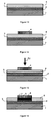
- the crystallization of a material is obtained from a substrate 1 formed, for example, by a crystalline material which, rendered amorphous, exhibits a glass transition phenomenon.
- the substrate 1 is, in particular, treated to form an amorphous upper portion 2 in the substrate 1.
- the arrows F1 represent, on the figure 2 , the processing step for rendering the upper portion 2 of the substrate 1 amorphous.
- the upper part 2 of the substrate 1 can be rendered amorphous by polishing or by ion implantation.
- a thin layer 3 consisting of a material to be crystallized is then deposited on the free surface of the upper part 2 of the substrate 1.
- the free surface of the upper part of the substrate can be cleaned beforehand, before the deposition of the thin layer 3.
- the thin layer 3 is deposited on the entire free surface of the upper part 2 of the substrate 1.
- the material to be crystallized is, more particularly, deposited in an amorphous or polycrystalline form. It can be of any type since it is able to crystallize in the solid phase. By way of example, it is a semiconductor material such as silicon, germanium, gallium arsenide (AsGa), gallium and indium arsenide (InGaAs), indium antimonide ( InSb). It can also be an insulating material such as an oxide, for example silicon oxide (SiO 2 ), boron oxide (B 2 O 3 ), titanium oxide (TiO 2 ), oxide tantalum (Ta 2 O 5 ) or it may be arsenic selenide (As 2 Se 3 ).
- a semiconductor material such as silicon, germanium, gallium arsenide (AsGa), gallium and indium arsenide (InGaAs), indium antimonide ( InSb).
- It can also be an insulating material such as an oxide, for example silicon oxide (SiO 2
- the deposition of the thin layer 3 can be of any known type.
- the thin layer 3 may be deposited by evaporation, by spraying possibly assisted by ion gun or magnetron.
- a metal layer 4 is deposited on an area of the free surface of the thin layer 3.
- the thickness of said metal layer 4 is between 1 nm and 20 nm, advantageously between 5 nm and 10 nm.
- the thickness of the metal layer is very small, for example of the order of 1 nm, it is not possible to have a metal layer other than in the form of a plurality of aggregates.
- the metal layer 4 is, in particular, constituted by a metal such as a metal used in catalysis (Ni, Pd, Pt), but not only. It may also be chosen from Cu, Ag, Cr, Au and Fe. In addition, the metal layer 4 may consist of a pure metal, a metal alloy or a mixture of metals (Ni + Cr, Ni + Au ). In a preferred embodiment, the metal layer 4 is not continuous, it is constituted by aggregates of the metal. In all embodiments, the metal layer 4 may be disposed over the entire surface of the substrate or only on areas where crystallization is desired. The thickness of the metal layer consisting of aggregates at a thickness which is equivalent in mass to that of a continuous layer between 1 and 20 nm, preferably between 3 and 10 nm.
- the metal layer 4 is not, in the context of the invention, intended to act as a catalyst to adjust the size of the grains in a controlled manner. It is the combination of said metal layer, preferentially in the form of aggregates, with a particular heat treatment allowing the upper part of the substrate to pass into a liquid or supercooled liquid state, advantageously without directly heating the thin layer to be crystallized. which allows, according to the invention, to obtain solid phase crystallization. More particularly, the metal layer 4 serves as a radiator for evacuating the heat in the thin layer to be crystallized, that is to say that it serves to remove heat from the thin layer to be crystallized radiatively .
- the layer to be crystallized changes to the liquid state and the process is no longer a "solid phase" process.
- the metal layer is constituted by aggregates
- a radiative heat emission is performed by the metal aggregates in interaction with the layer to be crystallized.
- the assembly consisting of the substrate 1, the thin layer 3 and the metal layer 4 undergoes heat treatment.
- the heat treatment is intended to bring heat to the upper part 2 of the substrate 1 and to cause a rapid rise in temperature in the upper part 2 of the substrate 1 and more generally in the substrate 1.
- the temperature of the upper part 2 of the substrate 1 rises, thus, at least to the glass transition zone, so that said upper portion 2 passes at least in the state of supercooled liquid.
- the rise in temperature of the upper part 2 of the substrate must be rapid, with a speed greater than 100K / s.
- Such a rise in temperature can be obtained by interacting, for example, with a continuous or pulsed laser beam on the upper part 2 of the substrate 1, through the metal layer 4 and the thin layer 3.
- the range of lengths emission wave of the laser beam corresponds to the absorption wavelength range of the upper part 2 of the substrate 1.
- the emission of the laser beam is partially or totally absorbed by the upper part 2 of the
- the emission wavelength range of the laser beam also corresponds to the range of wavelengths of transparency of the thin layer 3.
- the thin layer 3 does not absorb or slightly the lengths of light. wave of the laser beam, it is not heated directly.
- the laser beam is represented by the arrow F2 and is applied so as to pass through the metal layer 4 and the thin layer 3 before reaching the upper part 2 of the substrate.
- the laser beam may be a CO 2 laser emitting at 10.6 ⁇ m.
- the laser beam may be a CO 2 laser or a YAG laser, emitting at 1.064 microns. At this wavelength, amorphous silicon absorbs little (a few hundred cm -1 ) relative to the metal.
- the upper part 2 of the substrate passes from the solid state to a state of supercooled liquid and allows the crystallization of an area 5 of the thin layer 3, by thermal transfer.
- the zone 5 corresponds to the zone of the thin layer 3, placed under the metal layer 4, while the remainder of the thin layer 3, not covered by the thin metallic layer, is not crystallized ( figure 7 ).
- the metal layer 4 covers the entire thin layer 3 to crystallize, it can be fully crystallized.
- the figure 8 represents the temperature cycle applied to the upper part 2 of the substrate 1 as a function of time, in the embodiment shown in FIGS. Figures 1 to 7 .
- the temperature of the upper part 2 of the substrate 1 remains, for example, constant during the deposition of the thin layer 3, then increases rapidly during the heat treatment step.
- the increase in the temperature of the upper part 2 of the substrate 1 is, for example, linear and it goes beyond the glass transition temperature of the material of the upper part 2 of the substrate 1.
- the upper part 2 of the substrate 1 can be in any type of solid material, amorphous or capable of becoming by treatment, since the material is able to pass to the liquid state or supercooled liquid.
- the upper part 2 of the substrate 1 or even the whole of the substrate 1 can be amorphous before the crystallization process.
- the substrate or at least an upper part of the substrate may, for example, consist of a glass, such as an amorphous oxide, an amorphous semiconductor element or material or a non-crystalline polymer.
- the upper part of the substrate or even the whole of the substrate may also be, in the beginning of the process, in a crystalline form.
- the substrate can undergo, before the heat treatment, a treatment for obtaining at least an upper portion in amorphous form.
- the upper part of the substrate or the entire substrate may thus be rendered amorphous before the deposition of the thin film to be crystallized 3, before or after the deposition of the metal layer 4.
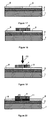
- a plurality of thin layers are successively deposited on the surface of the upper part 2 of the substrate 1.
- an additional thin layer 6 is deposited on the thin layer 3 to be crystallized, so as to obtain two superimposed thin layers.
- a metal layer 4 is then deposited on an area of the additional thin layer 6.
- the assembly, formed by the substrate 1, the two superimposed thin layers 6, 3 and the metal layer 4, is then subjected to a heat treatment (arrow F2 on the figure 15 ) for crystallizing not only the material of the thin layer 3 but also that of the additional thin layer 6.
- a heat treatment (arrow F2 on the figure 15 ) for crystallizing not only the material of the thin layer 3 but also that of the additional thin layer 6.
- an additional oxide for example a silicon oxide, of a few nanometers in thickness, for example 5 nm.
- This additional oxide layer (not shown) is disposed under the metal layer 4.
- the additional oxide layer makes it possible to promote the phenomenon of solid crystallization of the layer to crystallize amorphous located just below.
- crystallization by a single heat treatment step, a plurality of superimposed thin layers of distinct and crystalline materials.
- Such an embodiment is also called crystallization in series mode and it can in particular be used to produce heterostructures.
- the crystallization may even include the metal layer.
- the crystallization takes place under the metal layer 4 and its surroundings.
- the metal layer 4 covers the entire free surface of the additional thin layer 6, the layers 3 and 6 can be fully crystallized.
- a plurality of thin layers may be deposited on a plurality of areas of the surface of the upper portion 2 of the substrate 1, prior to the heat treatment.
- the surface of the upper part 2 is covered by two thin layers 8 and 9, adjacent and respectively constituted by separate materials to be crystallized, for example in monocrystalline form.
- a metal layer 4, having a thickness of between 1 nm and 20 nm, is then deposited on the stack, so as to advantageously cover part of the thin layer 8 and part of the thin layer 9 ( figure 18 ).
- the assembly formed by the substrate, the two adjacent thin layers 8 and 9 and the metal layer 4 then undergoes heat treatment (arrow F2 on the figure 19 ) for simultaneously crystallizing the respective materials of the thin layers 8 and 9 arranged under the metal layer 4.
- heat treatment arrow F2 on the figure 19
- crystallized zones 10 and 11 are obtained and corresponding to the respective zones of the thin layers 8 and 9 arranged under the metal layer 4.
- the two thin layers 8 and 9 may be successively deposited on the surface of the upper part 2 of the substrate.
- the thin layer 8 may be previously deposited on an area of the surface of the upper part 2 of the substrate, through a mask hiding the area to be covered by the second thin layer 8.
- the second thin layer is deposited on the free zone of the substrate, through a mask hiding the thin layer 8 already deposited.
- Such a variant is also called crystallization in parallel mode and is particularly adapted to combine the functionalities of several materials on the same substrate.
- a crystallization process according to the invention therefore makes it possible to crystallize a material of nanometric thickness.
- Such a method is relatively inexpensive because it does not require a crucible and it has a relatively low thermal budget since the heat input required for crystallization does not need to reach the melting temperature of the material to be crystallized.
- the crystallized thin layer may be in a different crystalline phase, with different physical properties from those synthesized by existing crystallization processes.
- Such a production method can be used in the field of nanotechnological processes, but also in the energy field and more particularly in the field of photovoltaic cells.
- the substrate is, for example, Corning glass for flat screens with a glass temperature of the order of 550 ° C. and a thickness of about 1 mm.
- the thin layer to be crystallized is, for example, of amorphous silicon deposited by vacuum evaporation, the thickness of the thin layer is equal to 500 nm and the temperature of the substrate during evaporation is equal to 400.degree.
- a silica layer, of a thickness of 5 nm, is deposited by evaporation under vacuum on the amorphous silicon layer.
- the metal layer formed by gold aggregates, is then deposited on the silicon oxide layer.
- the metal layer has an equivalent thickness equal to 5 nm. All these deposits can be made at the same substrate temperature in the same vacuum deposition equipment.
- the continuous CO 2 laser beam makes it possible to heat-treat the upper layer of the substrate.
- the emission wavelength of said laser is of the order of 10.59 microns, which corresponds to the emission line of the most powerful laser.
- This excitation wavelength is adapted to the absorption range of the upper layer of the substrate, which allows a rise in temperature of said upper layer. Indeed, in the glass, all emission lines of the CO 2 laser beam, (9.2 - 10.8 ⁇ m) can be used.
- the power stability of the excitation source is standard, typically of the order of ⁇ 3%, over the duration of the heat treatment.
- the laser emission mode can be any (Gaussian, flat, annular ...), but it must be stable. It is, advantageously, flat.
- the power required to perform the heat treatment is a linear power which depends on the characteristic dimensions of the laser beam and the physical properties of the amorphous top layer of the substrate (absorption, thermal conductivity, etc.), as well as the scanning speed. said beam.
- the incident laser power to achieve crystallization is typically 2 Watts, at the speed of 1 cm / s, interacting with the implementation device described above. above.
- the radiation of the CO 2 laser beam is incident on the front face of the stack formed by the layer of metal aggregates, the very thin layer of oxide, the thin layer to be crystallized and the substrate. It passes through the metal and the thin film to be crystallized, before being absorbed into the substrate and causing a rapid rise in the temperature of said substrate, with passage into the glass transition zone, which causes the crystallization of the silicon thin film .
- the device for controlling and stabilizing the power of the laser preferably comprises several elements: a laser power variator which can consist of a half wave plate followed by a polarizer.
- a laser power variator which can consist of a half wave plate followed by a polarizer.
- This device can be completed by a shutter and a laser power measuring device for verifying that the power setpoint is reached. It can even include a real-time stabilization device the power of the annealing laser.
- the shutter could be replaced by an "off-on" switching device of the laser source itself.
- the focusing lens is, for example, ZnSe and can be processed to be anti-reflective at the emission wavelength of the laser beam. Its focal length can be adapted to the desired focal spot on the thin layer to be crystallized. In addition, the dimensions of the focal spot on the surface of the stack can be determined by a so-called knife method.
- the lens may also be cylindrical, to produce a larger light brush in a direction perpendicular to the scanning direction. This makes it possible to cover a larger area of substrate per line of passage.
- the invention is not limited to the embodiments described above.
- the surface of the upper part 2 of the substrate 1 is not necessarily flat. It may, for example, be spherical, concave or convex, or it may comprise recessed areas and / or raised areas.
- said surface may be structured during its passage in the liquid state or supercooled liquid. This structuring can be induced by different mechanical processes, acoustic, lasers, ...
- Such a crystallization process can be applied to devices that require crystalline layers, such as electronic devices (diode, transistor, %), optical devices (mirror, spherical optics, %), photonic devices ( waveguide, %), ...
- the crystallization process is, in fact, intrinsically favorable to the crystallization of layers having a thickness ranging from nanometers to several hundreds of nanometers.
Abstract
Description
L'invention concerne un procédé de cristallisation.The invention relates to a crystallization process.
Il existe de nombreuses méthodes de cristallisation : la cristallisation d'un matériau à partir de sa phase vapeur, la cristallisation à partir de bains fondus ou la cristallisation à partir de solutions. Dans ces cas, le cristal apparaît par refroidissement lors de la transition liquide-solide ou lors de la transition vapeur-solide.There are many methods of crystallization: crystallization of a material from its vapor phase, crystallization from molten baths or crystallization from solutions. In these cases, the crystal appears by cooling during the liquid-solid transition or during the vapor-solid transition.
Plus particulièrement, des matériaux cristallisés sous une forme monocristalline peuvent être obtenus par croissance à partir d'un germe monocristallin. À titre d'exemple, des lingots en silicium monocristallin peuvent être obtenus par le procédé de Czochralski qui consiste à tremper un germe monocristallin, à la surface d'un bain de silicium faiblement surchauffé et à tirer le germe à vitesse continue. La solidification a lieu et reproduit le motif cristallin du germe jusqu'à l'obtention d'un lingot en silicium monocristallin. Le bain de silicium est contenu dans un creuset qui doit être formé par un matériau ayant un point de fusion supérieur à celui du silicium monocristallin. Il est, par exemple, en silice ou en nitrure de bore. Or, plus la température de fusion du monocristal est élevée, plus le volume de cristal est important, plus le coût du creuset devient prohibitif. De plus, il faut maintenir le bain liquide à la température de fusion pendant toute la durée de croissance du cristal, ce qui nécessite un apport énergétique important et contrôlé sur de longues périodes de temps. Enfin, les procédés actuels de cristallisation ne sont pas adaptés pour réaliser des cristaux sur de grandes surfaces.More particularly, materials crystallized in monocrystalline form can be obtained by growth from a monocrystalline seed. For example, monocrystalline silicon ingots can be obtained by the Czochralski method of dipping a monocrystalline seed on the surface of a slightly overheated silicon bath and pulling the seed at a continuous rate. The solidification takes place and reproduces the crystalline pattern of the seed until obtaining a monocrystalline silicon ingot. The silicon bath is contained in a crucible which must be formed by a material having a melting point higher than that of monocrystalline silicon. It is, for example, silica or boron nitride. However, the higher the melting temperature of the single crystal, the higher the volume of crystal, the more the cost of the crucible becomes prohibitive. In addition, it is necessary to maintain the liquid bath at the melting temperature throughout the growth period of the crystal, which requires a large and controlled energy intake over long periods of time. Finally, current methods of crystallization are not suitable for making crystals over large areas.
De plus, dans le cas d'un lingot de silicium monocristallin, obtenu par procédé de Czochralski, celui-ci doit subir un certain nombre d'étapes supplémentaires, avant de pouvoir être utilisé sous forme de tranches. Il doit, ainsi, être conditionné, découpé, poli, nettoyé... Or, ces traitements provoquent une perte de matière et affectent les propriétés physiques de la surface du silicium monocristallin. Ainsi, dans le domaine de la microélectronique, à l'issue du conditionnement, les tranches de silicium monocristallin sont d'une épaisseur supérieure à 100 µm, afin de permettre leur préhension et leur maniement robotisé. Or, l'épaisseur utilisée pour réaliser un dispositif microélectronique ne représente qu'une très faible proportion de l'épaisseur totale de la tranche. De tels procédés de cristallisation monocristalline ne sont donc pas adaptés pour réaliser des épaisseurs nanométriques.In addition, in the case of a monocrystalline silicon ingot obtained by the Czochralski process, it must undergo a number of additional steps, before it can be used in slices. It must, thus, be conditioned, cut, polished, cleaned ... Now, these treatments cause a loss of material and affect the physical properties of the surface of single crystal silicon. Thus, in the field of microelectronics, after packaging, monocrystalline silicon wafers have a thickness greater than 100 microns, to allow their gripping and robotic handling. However, the thickness used to make a microelectronic device represents only a very small proportion of the total thickness of the wafer. Such monocrystalline crystallization processes are therefore not suitable for producing nanometric thicknesses.
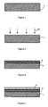
Des films minces polycristallins peuvent être obtenus par cristallisation, soit à partir de la phase liquide, soit à partir de la phase solide d'une couche amorphe.Thin polycrystalline films can be obtained by crystallization, either from the liquid phase or from the solid phase of an amorphous layer.
À titre d'exemple, la cristallisation, sous forme polycristalline, d'une couche amorphe de silicium, déposée sur un substrat, par exemple en verre, peut être réalisée à l'aide d'un faisceau laser pulsé, principalement un laser excimère. Dans ce cas, la cristallisation est réalisée après un passage en phase liquide, c'est-à-dire par voie liquide. L'énergie du laser est, en effet, absorbée localement par la couche à cristalliser, ce qui permet de porter le matériau à haute température, tandis que le substrat reste à une température relativement basse. Le polycristal apparaît, alors, lors du cycle de fusion-solidification. Lors de la croissance, dite SLG (ou « Super Lateral Growth »), la cristallisation de la zone exposée et chauffée par le laser débute par les parties externes de ladite zone, lesdites parties étant celles qui se refroidissent le plus vite à l'intérieur de la zone chauffée par le faisceau laser.By way of example, the crystallization, in polycrystalline form, of an amorphous layer of silicon deposited on a substrate, for example made of glass, can be carried out using a pulsed laser beam, mainly an excimer laser. In this case, the crystallization is performed after a passage in the liquid phase, that is to say by liquid. The energy of the laser is, in fact, absorbed locally by the layer to be crystallized, which makes it possible to carry the material at high temperature, while the substrate remains at a relatively low temperature. The polycristal appears, then, during the melting-solidification cycle. During growth, called SLG (or "Super Lateral Growth"), the crystallization of the exposed area heated by the laser begins with external portions of said zone, said portions being those which cool the fastest within the zone heated by the laser beam.
La dimension maximale des grains obtenus par cette technique de cristallisation en voie liquide est de l'ordre de 5 à 10 fois l'épaisseur de la couche à cristalliser. Or, les couches ont, en général, une épaisseur de quelques centaines de nanomètres d'épaisseur. Ainsi, cette technique s'applique, en général, à des couches très minces. De plus, c'est une technique difficile à mettre en oeuvre pour cristalliser une grande surface de façon homogène.The maximum grain size obtained by this liquid crystallization technique is of the order of 5 to 10 times the thickness of the layer to be crystallized. However, the layers are, in general, a thickness of a few hundred nanometers thick. Thus, this technique generally applies to very thin layers. In addition, it is a difficult technique to implement to crystallize a large area homogeneously.
Pour remédier à cet inconvénient, la demande de brevet
Une autre technique consiste à cristalliser le matériau en phase solide, c'est-à-dire sans passer par l'état liquide. La cristallisation en phase solide est, généralement, réalisée par recuit thermique conventionnel, également appelé SPC. Ainsi, l'empilement formé d'une couche amorphe déposée sur un substrat est soumis à un recuit, réalisé pendant une durée variant de plusieurs minutes à quelques heures, suivant la température et le type de matériau à cristalliser. Le matériau à cristalliser et le substrat sont, de plus, portés à la même température, qui est traditionnellement maintenue en dessous de la température de transition vitreuse ou de fusion du substrat.Another technique is to crystallize the solid phase material, that is to say without going through the liquid state. Solid phase crystallization is generally performed by conventional thermal annealing, also known as SPC. Thus, the stack formed of an amorphous layer deposited on a substrate is annealed for a time varying from several minutes to a few hours, depending on the temperature and the type of material to be crystallized. The material to be crystallized and the substrate are, moreover, brought to the same temperature, which is traditionally maintained below the glass transition temperature or melting of the substrate.
La cristallisation en phase solide peut, également, être favorisée par un dépôt de matériaux facilitant la germination des cristallites. Une telle technique, appelée recuit assisté par un métal ou « MIC », est décrite dans la demande de brevet
La demande de brevet
Cependant, le substrat en verre utilisé dans la demande de brevet
Il existe également des procédés de dépôt de matériaux sur un substrat, par pulvérisation réactive par magnétron ou par dépôt chimique en phase vapeur assisté par plasma (PECVD), qui permettent une cristallisation partielle du matériau sur le substrat. Cependant, avec ces techniques de dépôt, la dimension des grains obtenus est inférieure au micromètre, ce qui ne procure pas toujours au matériau les propriétés thermiques, optiques et électroniques optimales pour les applications voulues. A titre d'exemple,
L'invention a pour but un procédé de cristallisation remédiant aux inconvénients des procédés selon l'art antérieur. L'invention a, en particulier, pour but d'obtenir un matériau cristallisé de faible épaisseur, par exemple de l'ordre de la centaine de nanomètres, et de très grande surface, avec des propriétés homogènes sur toute ladite surface.The object of the invention is a crystallization process which overcomes the disadvantages of the processes according to the prior art. The object of the invention is, in particular, to obtain a crystallized material of small thickness, for example of the order of one hundred nanometers, and of very large surface area, with properties that are homogeneous over the entire surface.
Selon l'invention, ce but est atteint par les revendications annexées.According to the invention, this object is achieved by the appended claims.
Plus particulièrement, ce but est atteint par un procédé de cristallisation en phase solide comportant les étapes successives suivantes :
- a) dépôt d'au moins d'une couche mince en matériau amorphe ou polycristallin, sur au moins une zone de la surface d'une partie supérieure d'un substrat,
- b) dépôt d'au moins une couche métallique, d'une épaisseur comprise entre 1nm et 20nm, avantageusement entre 5nm et 10nm, sur une zone de ladite couche mince, la partie supérieure du substrat étant constituée, après l'étape b), par un matériau amorphe apte à passer dans un état liquide ou de liquide surfondu
- c) et traitement thermique pour permettre la croissance cristalline du matériau de la couche mince, en provoquant simultanément :
- une montée de la température de la partie supérieure du substrat à une vitesse supérieure à 100K par seconde, jusqu'à ce que le matériau de la partie supérieure du substrat passe à l'état liquide ou à l'état de liquide surfondu,
- et un transfert thermique depuis l'interface entre la partie supérieure du substrat et la couche mince vers l'interface entre la couche mince et la couche métallique.
- a) depositing at least one thin layer of amorphous or polycrystalline material on at least one area of the surface of an upper part of a substrate,
- b) deposition of at least one metal layer, of a thickness between 1 nm and 20 nm, advantageously between 5 nm and 10 nm, over an area of said thin layer, the upper part of the substrate being constituted, after step b), by an amorphous material capable of passing into a liquid state or supercooled liquid
- c) and heat treatment to allow crystal growth of the thin film material, simultaneously causing:
- a rise in the temperature of the upper part of the substrate at a speed greater than 100 K per second, until the material of the upper part of the substrate goes into the liquid state or the supercooled liquid state,
- and heat transfer from the interface between the top of the substrate and the thin layer to the interface between the thin layer and the metal layer.
Selon un développement de l'invention l'étape c) est réalisée par application d'un faisceau laser continu ou pulsé, présentant une gamme de longueurs d'onde d'émission correspondant à la gamme de longueurs d'onde d'absorption de la partie supérieure du substrat et à la gamme de longueurs d'onde de transparence du matériau amorphe ou polycristallin de la couche mince à cristalliser.According to a development of the invention step c) is carried out by applying a continuous or pulsed laser beam, having a range of emission wavelengths corresponding to the range of wavelengths of absorption of the upper part of the substrate and the wavelength range of transparency of the amorphous or polycrystalline material of the thin layer to be crystallized.
D'autres avantages et caractéristiques ressortiront plus clairement de la description qui va suivre de modes particuliers de réalisation de l'invention donnés à titre d'exemples non limitatifs et représentés aux dessins annexés, dans lesquels :
- Les
figures 1 à 7 représentent schématiquement, en coupe, différentes étapes d'un premier mode de réalisation d'un procédé selon l'invention. - La
figure 8 représente le cycle en température appliqué à la partie supérieure du substrat en fonction du temps, pendant ledit premier mode de réalisation. - Les
figures 9 à 12 représentent schématiquement, en coupe, une variante de réalisation dudit premier mode de réalisation. - Les
figures 13 à 16 représentent, schématiquement, en coupe, différentes étapes d'un troisième mode de réalisation d'un procédé selon l'invention. - Les
figures 17 à 20 représentent, schématiquement, en coupe, différentes étapes d'un quatrième mode de réalisation d'un procédé selon l'invention.
- The
Figures 1 to 7 schematically represent, in section, different steps of a first embodiment of a method according to the invention. - The
figure 8 represents the temperature cycle applied to the upper part of the substrate as a function of time, during said first embodiment. - The
Figures 9 to 12 schematically represent, in section, an alternative embodiment of said first embodiment. - The
Figures 13 to 16 show schematically, in section, different steps of a third embodiment of a method according to the invention. - The
Figures 17 to 20 show schematically, in section, different steps of a fourth embodiment of a method according to the invention.
Un procédé de cristallisation comporte une étape de dépôt d'au moins une couche mince, en un matériau amorphe ou polycristallin destiné à être cristallisé par exemple sous forme monocristalline, sur au moins une zone de la surface d'une partie supérieure d'un substrat. L'étape de dépôt de la couche mince est suivie d'une étape de dépôt d'au moins une couche métallique, sur une zone de ladite couche mince en matériau amorphe ou polycristallin. La couche métallique a une épaisseur comprise entre 1nm et 20nm, avantageusement entre 5nm et 10nm. Puis, une étape de traitement thermique est réalisée. Dans certaines conditions, une atmosphère réductrice, inerte ou oxydante peut être prévue lors du traitement thermique.A crystallization process comprises a step of depositing at least one thin layer, made of an amorphous or polycrystalline material intended to be crystallized, for example in monocrystalline form, on at least one area of the surface of an upper part of a substrate . The deposition step of the thin layer is followed by a step of deposition of at least one metal layer on an area of said thin layer of amorphous or polycrystalline material. The metal layer has a thickness of between 1 nm and 20 nm, advantageously between 5 nm and 10 nm. Then, a heat treatment step is performed. Under certain conditions, a reducing, inert or oxidizing atmosphere may be provided during the heat treatment.
Par ailleurs, la partie supérieure du substrat est constituée par un matériau distinct du matériau à cristalliser. Le matériau de la partie supérieure du substrat est, de plus, amorphe avant le traitement thermique et il est apte à passer à l'état de liquide ou à l'état de liquide surfondu.Moreover, the upper part of the substrate consists of a material distinct from the material to be crystallized. The material of the upper part of the substrate is, moreover, amorphous before the heat treatment and is able to pass to the state of liquid or the state of supercooled liquid.
La partie supérieure du substrat est, par exemple, constituée avant l'étape de traitement thermique, par un matériau amorphe tel que :
- un verre, par exemple les verres à base d'oxyde (oxyde de silicium (SiO2), borosilicate (B2O3,SiO2),) et les verres à base de chalcogénure (tel que As2Se3) ou des céramiques comme l'alumine (Al2O3)...
- ou un polymère non cristallin tel que le polycarbonate.
- a glass, for example glasses based on oxide (silicon oxide (SiO 2 ), borosilicate (B 2 O 3 , SiO 2 ),) and chalcogenide-based glasses (such as As 2 Se 3 ) or ceramics such as alumina (Al 2 O 3 ) ...
- or a non-crystalline polymer such as polycarbonate.
Dans ce cas, ledit matériau amorphe peut être soumis à un phénomène de transition vitreuse.In this case, said amorphous material may be subjected to a glass transition phenomenon.
En effet, dans le cas d'un verre, l'étude de la variation d'une grandeur thermodynamique, telle que la chaleur spécifique volumique, permet de constater que, lors du refroidissement de la phase liquide stable, si la viscosité est trop importante ou si le refroidissement est très rapide, la cristallisation n'a pas le temps de se produire et un liquide surfondu est obtenu. La zone de température dans laquelle est obtenu le liquide surfondu correspond à la zone de transition vitreuse. De plus, en poursuivant le refroidissement, la viscosité du liquide augmente fortement et le liquide surfondu devient quasiment solide. Or, lorsque la viscosité atteint 1013 poises, la rigidité empêche les mouvements microscopiques locaux et un changement de pente de la grandeur étudiée est observé. La température à laquelle se produit ce changement correspond à la température de transition vitreuse du matériau (Tg). Ainsi, pour une température inférieure à la température de transition vitreuse, le matériau est dit solide avec le désordre structural d'un liquide, tandis qu'au-dessus de la température de fusion, le matériau est dit à l'état liquide. Par zone de transition vitreuse, on entend donc une plage de température, délimitée par la température de fusion et par la température de transition vitreuse dudit matériau. Cette zone de transition vitreuse correspond au passage de l'état solide à l'état liquide du matériau. Dans cette zone de température dite zone de transition ou zone de transition vitreuse, le matériau est considéré à l'état de liquide surfondu.Indeed, in the case of a glass, the study of the variation of a thermodynamic quantity, such as the specific heat density, makes it possible to observe that, during the cooling of the stable liquid phase, if the viscosity is too high or if the cooling is very fast, the crystallization does not have time to occur and a supercooled liquid is obtained. The temperature zone in which the supercooled liquid is obtained corresponds to the glass transition zone. In addition, by continuing the cooling, the viscosity of the liquid increases strongly and the supercooled liquid becomes almost solid. However, when the viscosity reaches 10 13 poises, rigidity prevents local microscopic movements and a change in slope of the studied quantity is observed. The temperature at which this change occurs corresponds to the glass transition temperature of the material (Tg). Thus, for a temperature below the glass transition temperature, the material is said to be solid with the structural disorder of a liquid, while above the melting temperature the material is said to be in the liquid state. By glass transition zone is therefore meant a temperature range, delimited by the melting temperature and the glass transition temperature of said material. This glass transition zone corresponds to the transition from the solid state to the liquid state of the material. In this zone of temperature called transition zone or glass transition zone, the material is considered in the state of supercooled liquid.
Plutôt que d'être en verre ou en polymère non cristallin, la partie supérieure du substrat peut également être constituée par un métal (par exemple Fe, Cu, Ti...) ou un alliage métallique (par exemple de l'acier inoxydable), amorphe avant l'étape de traitement thermique. Dans ce cas, la zone de transition correspond à la température de fusion du matériau constituant la partie supérieure du substrat.Rather than being made of glass or non-crystalline polymer, the upper part of the substrate may also consist of a metal (for example Fe, Cu, Ti ...) or a metal alloy (for example stainless steel) , amorphous before the heat treatment step. In this case, the transition zone corresponds to the melting temperature of the material constituting the upper part of the substrate.
Par ailleurs, le matériau constituant la partie supérieure du substrat peut être le même matériau que celui constituant la couche mince à cristalliser, les deux matériaux présentant, alors, préférentiellement, des états de structure différents. Par exemple, le matériau constituant la partie supérieure du substrat peut être sous forme amorphe, tandis que celui constituant la couche mince à cristalliser peut être sous forme polycristalline. Cependant, de manière avantageuse, le matériau de la partie supérieure du substrat est distinct du matériau amorphe ou polycristallin à cristalliser.Furthermore, the material constituting the upper part of the substrate may be the same material as that constituting the thin layer to be crystallized, the two materials then having, preferably, different states of structure. For example, the material constituting the upper part of the substrate may be in amorphous form, whereas that constituting the thin layer to be crystallized may be in polycrystalline form. However, advantageously, the material of the upper part of the substrate is distinct from the amorphous or polycrystalline material to be crystallized.
Ainsi, dans le procédé de cristallisation selon l'invention, l'étape de traitement thermique est destinée à provoquer une montée très rapide de la température de la partie supérieure du substrat, avantageusement sans chauffer directement la couche mince à cristalliser. La montée en température, également appelée rampe thermique, est réalisée à une vitesse supérieure à 100K par seconde et elle est réalisée jusqu'à ce que la partie supérieure du substrat atteigne la zone de transition. Ainsi, la montée en température est réalisée jusqu'à ce que la partie supérieure du substrat passe dans un état de liquide ou dans un état de liquide surfondu.Thus, in the crystallization process according to the invention, the heat treatment step is intended to cause a very rapid rise in the temperature of the upper part of the substrate, preferably without directly heating the thin layer to be crystallized. The rise in temperature, also called thermal ramp, is performed at a speed greater than 100K per second and is performed until the upper part of the substrate reaches the transition zone. Thus, the rise in temperature is carried out until the upper part of the substrate goes into a liquid state or into a supercooled liquid state.
Le traitement thermique est, avantageusement, réalisé par un faisceau laser polarisé, dont l'énergie est absorbée par la partie supérieure du substrat. Par contre, contrairement à un procédé de cristallisation par voie liquide, dans le cadre de l'invention, le faisceau laser ne chauffe pas directement la couche mince à cristalliser, mais la partie supérieure du substrat. Ainsi, la couche mince à cristalliser ne passe pas dans un état liquide, mais reste dans un état solide. Ainsi, bien qu'utilisant avantageusement un faisceau laser, le procédé de cristallisation est un procédé de cristallisation par voie solide.The heat treatment is advantageously carried out by a polarized laser beam whose energy is absorbed by the upper part of the substrate. By cons, unlike a liquid crystallization process, in the context of the invention, the laser beam does not directly heat the thin layer to crystallize, but the upper part of the substrate. Thus, the thin layer to be crystallized does not pass into a liquid state, but remains in a solid state. Thus, although advantageously using a laser beam, the crystallization process is a solid-crystallization process.
L'apport de chaleur du faisceau laser est, en effet, suffisant pour que la partie supérieure du substrat passe de l'état solide à l'état de liquide ou de liquide surfondu. Par contre, la couche mince à cristalliser reste, avantageusement, « froide », afin que le flux thermique soit initialement le plus intense possible, entre la partie supérieure du substrat et la couche mince à cristalliser. Autrement dit, la couche mince à cristalliser n'absorbe pratiquement pas l'énergie émise par le faisceau laser.The heat input of the laser beam is, in fact, sufficient for the upper part of the substrate to change from the solid state to the state of liquid or supercooled liquid. On the other hand, the thin layer to be crystallized remains, advantageously, "cold", so that the heat flow is initially the more intense possible, between the upper part of the substrate and the thin layer to be crystallized. In other words, the thin layer to be crystallized practically does not absorb the energy emitted by the laser beam.
Pour obtenir une montée rapide de la température de la partie supérieure du substrat, sans chauffer directement la couche mince à cristalliser, le faisceau laser utilisé lors de l'étape de traitement thermique présente, avantageusement, une gamme de longueurs d'onde d'émission correspondant :
- à la gamme de longueurs d'onde d'absorption de la partie supérieure du substrat
- et à la gamme de longueurs d'onde de transparence du matériau amorphe ou polycristallin à cristalliser.
- to the wavelength range of absorption of the upper part of the substrate
- and at the wavelength range of transparency of the amorphous or polycrystalline material to be crystallized.
Par ailleurs, le faisceau laser peut également être continu ou pulsé et il peut être un laser CO2 ou YAG.Moreover, the laser beam can also be continuous or pulsed and it can be a CO 2 or YAG laser.
De plus, l'étape de traitement thermique doit provoquer, simultanément le passage de la partie supérieure du substrat en phase liquide ou liquide surfondu, et un transfert thermique à travers la couche mince à cristalliser, depuis l'interface de ladite couche avec le substrat vers l'interface de ladite couche et la couche métallique.In addition, the heat treatment step must simultaneously cause the passage of the upper part of the substrate in supercooled liquid or liquid phase, and a thermal transfer through the thin layer to be crystallized, from the interface of said layer with the substrate. to the interface of said layer and the metal layer.
Or, pour obtenir un flux thermique le plus intense possible, le coefficient d'absorption de la partie supérieure du substrat est, avantageusement, trois fois supérieur à celui de la couche mince à cristalliser, dans la gamme de longueurs d'onde d'émission du faisceau laser.However, in order to obtain the highest possible thermal flux, the absorption coefficient of the upper part of the substrate is advantageously three times greater than that of the thin layer to be crystallized, in the range of emission wavelengths. of the laser beam.
En effet, il a été trouvé, de manière surprenante, que le transfert thermique de la chaleur depuis la partie supérieure du substrat à travers la couche mince à cristalliser provoque une mise en contrainte de la couche mince à cristalliser. Or, cette mise en contrainte est d'autant plus intense que la rampe thermique est rapide et que la différence de température instantanée entre le substrat et la couche est importante. De plus, cette redistribution de la contrainte initiale favorise thermodynamiquement la cristallisation, puisqu'il y a alors réduction du volume molaire de la couche mince à cristalliser, qui tend vers celui de la phase cristalline.Indeed, it has been found, surprisingly, that the thermal transfer of heat from the upper part of the substrate through the thin layer to be crystallized causes stressing of the thin layer to be crystallized. However, this enforcement is all the more intense as the Thermal ramp is fast and the instantaneous temperature difference between the substrate and the layer is important. In addition, this redistribution of the initial stress thermodynamically promotes crystallization, since there is then a reduction in the molar volume of the thin layer to be crystallized, which tends towards that of the crystalline phase.
Le flux thermique doit être maintenu, afin que la croissance cristalline « à l'état solide» puisse se poursuivre. Pour cela, la chaleur issue de la partie supérieure du substrat ainsi que l'enthalpie de cristallisation doivent pouvoir être évacuées en surface de la couche mince en train de cristalliser. Cette évacuation est réalisée de manière radiative par la couche métallique.The heat flux must be maintained so that the "solid state" crystal growth can continue. For this, the heat from the upper part of the substrate and the enthalpy of crystallization must be able to be discharged to the surface of the thin layer being crystallized. This evacuation is carried out radiatively by the metal layer.
Lors de la redescente en température, la zone surfondue du substrat s'adapte à la densification de la couche cristallisée, avant de passer à l'état solide.During the temperature reduction, the supercooled zone of the substrate adapts to the densification of the crystallized layer before going into the solid state.
Selon un premier mode de réalisation, représenté sur les
Comme illustré sur la
Le matériau à cristalliser est, plus particulièrement, déposé sous une forme amorphe ou polycristalline. Il peut être de tout type dès lors qu'il est apte à cristalliser en phase solide. À titre d'exemple, il est un matériau semi-conducteur tel que le silicium, le germanium, l'arséniure de gallium (AsGa), l'arséniure de gallium et d'indium (InGaAs), l'antimoniure d'indium (InSb). Il peut également être un matériau isolant tel qu'un oxyde, par exemple l'oxyde de silicium (SiO2), l'oxyde de bore (B2O3), l'oxyde de titane (TiO2), l'oxyde de tantale (Ta2O5) ou bien il peut être du séléniure d'arsenic (As2Se3).The material to be crystallized is, more particularly, deposited in an amorphous or polycrystalline form. It can be of any type since it is able to crystallize in the solid phase. By way of example, it is a semiconductor material such as silicon, germanium, gallium arsenide (AsGa), gallium and indium arsenide (InGaAs), indium antimonide ( InSb). It can also be an insulating material such as an oxide, for example silicon oxide (SiO 2 ), boron oxide (B 2 O 3 ), titanium oxide (TiO 2 ), oxide tantalum (Ta 2 O 5 ) or it may be arsenic selenide (As 2 Se 3 ).
De plus, le dépôt de la couche mince 3 peut être de tout type connu. Par exemple, la couche mince 3 peut être déposée par évaporation, par pulvérisation éventuellement assistée par canon à ions ou par magnétron.In addition, the deposition of the
Puis, comme représenté sur la
La couche métallique 4 est, en particulier, constituée par un métal tel qu'un métal utilisé en catalyse (Ni, Pd, Pt), mais pas seulement. Il peut également être choisi parmi Cu, Ag, Cr, Au, Fe.... De plus, la couche métallique 4 peut être constituée par un métal pur, un alliage métallique ou un mélange de métaux (Ni+Cr, Ni+Au...). Dans un mode de réalisation privilégié, la couche métallique 4 n'est pas continue, elle est constituée par des agrégats du métal. Dans tous les modes de réalisation, la couche métallique 4 peut être disposée sur toute la surface du substrat ou seulement sur des zones où la cristallisation est recherchée. L'épaisseur de la couche métallique constituée par des agrégats à une épaisseur qui est équivalente en masse à celle d'une couche continue comprise entre 1 et 20nm, avantageusement entre 3 et 10nm.The
Par ailleurs, contrairement à l'enseignement du document
Puis, comme représenté sur les
Une telle montée en température peut être obtenue en faisant interagir, par exemple, un faisceau laser continu ou pulsé sur la partie supérieure 2 du substrat 1, à travers la couche métallique 4 et la couche mince 3. Dans ce cas, la gamme de longueurs d'onde d'émission du faisceau laser correspond à la gamme de longueurs d'onde d'absorption de la partie supérieure 2 du substrat 1. Ainsi, l'émission du faisceau laser est en partie ou totalement absorbée par la partie supérieure 2 du substrat 1. Par contre, la gamme de longueurs d'onde d'émission du faisceau laser correspond également à la gamme de longueurs d'onde de transparence de la couche mince 3. La couche mince 3 n'absorbant pas ou peu les longueurs d'onde du faisceau laser, elle n'est pas chauffée directement. Sur la
À titre d'exemple, pour une partie supérieure 2 en silice et une couche mince 3 à cristalliser en germanium, le faisceau laser peut être un laser CO2 émettant à 10,6µm. Selon un autre exemple, pour une partie supérieure 2 métallique et une couche mince 3 à cristalliser en silicium, le faisceau laser peut être un laser CO2 ou un laser YAG, émettant à 1,064 µm. À cette longueur d'onde, le silicium amorphe absorbe peu (quelques centaines de cm-1) par rapport au métal.For example, for a silica
Ainsi, pendant le traitement thermique, la partie supérieure 2 du substrat passe de l'état solide à un état de liquide surfondu et permet la cristallisation d'une zone 5 de la couche mince 3, par transfert thermique. La zone 5 correspond à la zone de la couche mince 3, disposée sous la couche métallique 4, tandis que le reste de la couche mince 3, non recouvert par la couche mince métallique, n'est pas cristallisé (
À titre d'exemple, la
La partie supérieure 2 du substrat 1 peut être en tout type de matériau solide, amorphe ou apte à le devenir par traitement, dès lors que le matériau est apte à passer à l'état liquide ou de liquide surfondu. Ainsi, la partie supérieure 2 du substrat 1 ou même la totalité du substrat 1 peut être amorphe avant le procédé de cristallisation. Le substrat ou au moins une partie supérieure du substrat peut, par exemple, être constitué par un verre, tel qu'un oxyde amorphe, un élément ou un matériau semi-conducteur amorphe ou par un polymère non cristallin. Comme l'illustre le mode de réalisation représenté par les
Ainsi, comme illustré dans une variante de réalisation représentée sur les
- un traitement mécanique tel qu'un polissage, un sablage,
- un traitement thermique tel qu'une fusion suivie d'une trempe,
- un traitement physico-chimique tel qu'un dépôt en phase vapeur ou une implantation ionique.
- a mechanical treatment such as polishing, sanding,
- a heat treatment such as a melting followed by quenching,
- a physicochemical treatment such as vapor phase deposition or ion implantation.
Dans un autre mode de réalisation illustré sur les
Selon un développement privilégié de l'invention, il est avantageux de prévoir le dépôt d'un oxyde additionnel, par exemple un oxyde de silicium, de quelques nanomètres d'épaisseur, par exemple 5 nm. Cette couche d'oxyde additionnel (non représentée) est disposée sous la couche métallique 4. La couche d'oxyde additionnel permet de favoriser le phénomène de cristallisation solide de la couche à cristalliser amorphe située juste au-dessous.According to a preferred development of the invention, it is advantageous to provide the deposition of an additional oxide, for example a silicon oxide, of a few nanometers in thickness, for example 5 nm. This additional oxide layer (not shown) is disposed under the
Il est, ainsi, possible de cristalliser, par une étape unique de traitement thermique, une pluralité de couches minces superposées en matériaux distincts et cristallins. Un tel mode de réalisation est également appelé cristallisation en mode série et il peut notamment être utilisé pour réaliser des hétérostructures. La cristallisation peut même inclure la couche métallique. De plus, la cristallisation a lieu sous la couche métallique 4 et à ses abords. De plus, si la couche métallique 4 recouvre la totalité de la surface libre de la couche mince supplémentaire 6, les couches 3 et 6 peuvent être totalement cristallisées.It is thus possible to crystallize, by a single heat treatment step, a plurality of superimposed thin layers of distinct and crystalline materials. Such an embodiment is also called crystallization in series mode and it can in particular be used to produce heterostructures. The crystallization may even include the metal layer. In addition, the crystallization takes place under the
Dans une variante représentée sur les
Il est, alors, possible de cristalliser, en une seule étape de traitement thermique, une pluralité de couches minces adjacentes. Plus particulièrement, les deux couches minces 8 et 9 peuvent être successivement déposées sur la surface de la partie supérieure 2 du substrat. Ainsi, la couche mince 8 peut être préalablement déposée sur une zone de la surface de la partie supérieure 2 du substrat, à travers un masque cachant la zone destinée à être recouverte par la deuxième couche mince 8. Puis, la deuxième couche mince est déposée sur la zone libre du substrat, à travers un masque cachant la couche mince 8 déjà déposée. Une telle variante est, également appelée cristallisation en mode parallèle et elle est, particulièrement, adaptée pour associer les fonctionnalités de plusieurs matériaux sur un même substrat.It is then possible to crystallize, in a single heat treatment step, a plurality of adjacent thin layers. More particularly, the two
Un procédé de cristallisation selon l'invention permet donc de cristalliser un matériau d'épaisseur nanométrique. Contrairement au procédé de Czochralski, il est, alors, possible d'obtenir des couches minces cristallines de très faible épaisseur, par exemple d'une épaisseur de l'ordre d'une centaine de nanomètres, sans nécessiter d'étapes supplémentaires de conditionnement.A crystallization process according to the invention therefore makes it possible to crystallize a material of nanometric thickness. In contrast to the Czochralski process, it is then possible to obtain very thin crystalline thin layers, for example of a thickness of the order of a hundred nanometers, without requiring additional conditioning steps.
De plus, un tel procédé permet d'obtenir des couches minces cristallines de très grande surface et avantageusement monocristallines, avec des propriétés homogènes sur toute ladite surface.In addition, such a method makes it possible to obtain crystalline thin films of very large surface area and advantageously monocrystalline, with homogeneous properties on all said surface.
Un tel procédé est relativement peu coûteux, car il ne nécessite pas de creuset et il présente un budget thermique relativement faible puisque l'apport de chaleur nécessaire à la cristallisation n'a pas besoin d'atteindre la température de fusion du matériau à cristalliser.Such a method is relatively inexpensive because it does not require a crucible and it has a relatively low thermal budget since the heat input required for crystallization does not need to reach the melting temperature of the material to be crystallized.
Enfin, la couche mince cristallisée peut être dans une phase cristalline différente, avec des propriétés physiques différentes de celles synthétisées par les procédés de cristallisation existants. Un tel procédé de réalisation peut être utilisé dans le domaine des procédés nanotechnologiques, mais également dans le domaine énergétique et plus particulièrement dans le domaine des cellules photovoltaïques.Finally, the crystallized thin layer may be in a different crystalline phase, with different physical properties from those synthesized by existing crystallization processes. Such a production method can be used in the field of nanotechnological processes, but also in the energy field and more particularly in the field of photovoltaic cells.
A titre d'exemple, un dispositif de mise en oeuvre du procédé de cristallisation peut comporter :
- une source laser CO2 émettant un faisceau laser continu
- un dispositif de contrôle et de stabilité de la puissance du faisceau laser
- une lentille de focalisation destinée à focaliser le faisceau laser sur le substrat muni d'une couche mince à cristalliser et d'une couche métallique, préalablement déposées sur ledit substrat
- et un dispositif de déplacement dudit substrat ou du faisceau laser, de manière à pouvoir traiter thermiquement l'ensemble de la surface du substrat.
- a CO 2 laser source emitting a continuous laser beam
- a device for controlling and stabilizing the power of the laser beam
- a focusing lens for focusing the laser beam on the substrate provided with a thin layer to be crystallized and a metal layer, previously deposited on said substrate
- and a device for moving said substrate or the laser beam so as to be able to heat-treat the entire surface of the substrate.
Le substrat est, par exemple, du verre Corning pour écrans plats, de température vitreuse de l'ordre de 550°C et d'une épaisseur de l'ordre de 1 mm. La couche mince à cristalliser est, par exemple, en silicium amorphe déposé par évaporation sous vide, l'épaisseur de la couche mince est égale à 500nm et la température du substrat lors de l'évaporation est égale à 400°C. Une couche de silice, d'une épaisseur de 5nm, est déposée par évaporation sous vide sur la couche de silicium amorphe. La couche métallique, formée par des agrégats d'or, est ensuite déposée sur la couche d'oxyde de silicium. La couche métallique a une épaisseur équivalent égale à 5nm.. Tous ces dépôts peuvent être réalisés à la même température de substrat dans un même équipement de dépôt sous vide.The substrate is, for example, Corning glass for flat screens with a glass temperature of the order of 550 ° C. and a thickness of about 1 mm. The thin layer to be crystallized is, for example, of amorphous silicon deposited by vacuum evaporation, the thickness of the thin layer is equal to 500 nm and the temperature of the substrate during evaporation is equal to 400.degree. A silica layer, of a thickness of 5 nm, is deposited by evaporation under vacuum on the amorphous silicon layer. The metal layer, formed by gold aggregates, is then deposited on the silicon oxide layer. The metal layer has an equivalent thickness equal to 5 nm. All these deposits can be made at the same substrate temperature in the same vacuum deposition equipment.
Le faisceau laser CO2 continu permet de réaliser un traitement thermique de la couche supérieure du substrat. La longueur d'onde d'émission dudit laser est de l'ordre de 10,59 µm, ce qui correspond à la raie d'émission du laser la plus puissante. Cette longueur d'onde d'excitation est adaptée à la gamme d'absorption de la couche supérieure du substrat, ce qui permet une montée en température de ladite couche supérieure. En effet, dans le verre, toutes les raies d'émission du faisceau laser CO2, (9,2 - 10,8 µm) peuvent être utilisées. La stabilité en puissance de la source d'excitation est standard, typiquement de l'ordre de ±3%, sur la durée du traitement thermique. De plus, le mode d'émission laser peut être quelconque (gaussien, plat, annulaire ...), mais il doit être stable. Il est, avantageusement, plat. Enfin, la puissance nécessaire pour effectuer le traitement thermique est une puissance linéique qui dépend des dimensions caractéristiques du faisceau laser et des propriétés physiques de la couche supérieure amorphe du substrat (absorption, conductivité thermique ...), ainsi que de la vitesse de balayage dudit faisceau. Pour un faisceau laser gaussien de diamètre à 1/e de 300 µm, la puissance laser incidente pour réussir la cristallisation est typiquement de 2 Watts, à la vitesse de 1 cm/s, en interaction avec le dispositif de mise en oeuvre décrit ci-dessus.The continuous CO 2 laser beam makes it possible to heat-treat the upper layer of the substrate. The emission wavelength of said laser is of the order of 10.59 microns, which corresponds to the emission line of the most powerful laser. This excitation wavelength is adapted to the absorption range of the upper layer of the substrate, which allows a rise in temperature of said upper layer. Indeed, in the glass, all emission lines of the CO 2 laser beam, (9.2 - 10.8 μm) can be used. The power stability of the excitation source is standard, typically of the order of ± 3%, over the duration of the heat treatment. In addition, the laser emission mode can be any (Gaussian, flat, annular ...), but it must be stable. It is, advantageously, flat. Finally, the power required to perform the heat treatment is a linear power which depends on the characteristic dimensions of the laser beam and the physical properties of the amorphous top layer of the substrate (absorption, thermal conductivity, etc.), as well as the scanning speed. said beam. For a Gaussian laser beam of
Ainsi, le rayonnement du faisceau laser CO2 est incident en face avant de l'empilement formé par la couche d'agrégats métalliques, la couche très mince d'oxyde, la couche mince à cristalliser et le substrat. Il traverse le métal et la couche mince à cristalliser, avant d'être absorbé dans le substrat et provoquer une montée rapide de la température dudit substrat, avec passage dans la zone de transition vitreuse, ce qui provoque la cristallisation de la couche mince en silicium.Thus, the radiation of the CO 2 laser beam is incident on the front face of the stack formed by the layer of metal aggregates, the very thin layer of oxide, the thin layer to be crystallized and the substrate. It passes through the metal and the thin film to be crystallized, before being absorbed into the substrate and causing a rapid rise in the temperature of said substrate, with passage into the glass transition zone, which causes the crystallization of the silicon thin film .
Le dispositif de contrôle et de stabilité de la puissance du laser comprend, de préférence, plusieurs éléments : un variateur de puissance laser qui peut être constitué d'une lame demi onde suivie d'un polariseur. Un tel dispositif permet d'ajuster la puissance d'excitation à une consigne et donc de faire varier la puissance appliquée au substrat à traiter thermiquement. Ce dispositif peut être complété par un obturateur et par un dispositif de mesure de la puissance laser destiné à vérifier que la consigne de puissance est bien atteinte. Il peut même inclure un dispositif de stabilisation en temps réel de la puissance du laser de recuit. L'obturateur pourrait être remplacé par un dispositif de commutation « éteint-allumé » de la source laser elle-même.The device for controlling and stabilizing the power of the laser preferably comprises several elements: a laser power variator which can consist of a half wave plate followed by a polarizer. Such a device makes it possible to adjust the excitation power to a setpoint and thus to vary the power applied to the substrate to be heat-treated. This device can be completed by a shutter and a laser power measuring device for verifying that the power setpoint is reached. It can even include a real-time stabilization device the power of the annealing laser. The shutter could be replaced by an "off-on" switching device of the laser source itself.
La lentille de focalisation est, par exemple, en ZnSe et elle peut être traitée pour être anti-reflet à la longueur d'onde d'émission du faisceau laser. Sa distance focale peut être adaptée à la tache focale souhaitée sur la couche mince à cristalliser. De plus, les dimensions de la tache focale, à la surface de l'empilement, peuvent être déterminées par une méthode dite du couteau. La lentille peut également être cylindrique, afin de produire un pinceau lumineux plus étendu dans une direction perpendiculaire au sens de balayage. Ceci permet de couvrir une plus grande surface de substrat par ligne de passage.The focusing lens is, for example, ZnSe and can be processed to be anti-reflective at the emission wavelength of the laser beam. Its focal length can be adapted to the desired focal spot on the thin layer to be crystallized. In addition, the dimensions of the focal spot on the surface of the stack can be determined by a so-called knife method. The lens may also be cylindrical, to produce a larger light brush in a direction perpendicular to the scanning direction. This makes it possible to cover a larger area of substrate per line of passage.
L'invention n'est pas limitée aux modes de réalisation décrits ci-dessus. La surface de la partie supérieure 2 du substrat 1 n'est pas nécessairement plane. Elle peut, par exemple, être sphérique, concave ou convexe, ou bien elle peut comporter des zones en creux et/ou des zones en relief. De plus, ladite surface peut être structurée lors de son passage à l'état liquide ou de liquide surfondu. Cette structuration peut être induite par différents procédés mécaniques, acoustiques, lasers, ...The invention is not limited to the embodiments described above. The surface of the
Un tel procédé de cristallisation peut être appliqué à des dispositifs qui nécessitent des couches cristallines, tels que des dispositifs électroniques (diode, transistor, ...), des dispositifs optiques (miroir, optique sphérique,...), des dispositifs photoniques (guide d'onde,...),...Such a crystallization process can be applied to devices that require crystalline layers, such as electronic devices (diode, transistor, ...), optical devices (mirror, spherical optics, ...), photonic devices ( waveguide, ...), ...
Le procédé de cristallisation est, en effet, intrinsèquement favorable à la cristallisation des couches ayant une épaisseur allant de l'ordre du nanomètre jusqu'à plusieurs centaines de nanomètres. Cependant, pour cristalliser une couche plus épaisse ou obtenir de nouvelles phases cristallines, il peut être avantageux de refroidir initialement l'empilement formé par le substrat, la couche mince à cristalliser et la couche métallique, afin de faciliter le transfert thermique du substrat à travers la couche amorphe que l'on désire cristalliser jusqu'à la couche métallique de surface.The crystallization process is, in fact, intrinsically favorable to the crystallization of layers having a thickness ranging from nanometers to several hundreds of nanometers. However, to crystallize a thicker layer or obtain new crystalline phases, it may be advantageous to initially cool the stack formed by the substrate, the thin layer to be crystallized and the metal layer, to facilitate the thermal transfer of the substrate through the amorphous layer that is desired to crystallize to the surface metal layer.
Claims (13)
Applications Claiming Priority (1)
| Application Number | Priority Date | Filing Date | Title |
|---|---|---|---|
| PCT/FR2007/001965 WO2009068756A1 (en) | 2007-11-28 | 2007-11-28 | Crystallisation method |
Publications (2)
| Publication Number | Publication Date |
|---|---|
| EP2071058A1 true EP2071058A1 (en) | 2009-06-17 |
| EP2071058B1 EP2071058B1 (en) | 2011-07-13 |
Family
ID=39855108
Family Applications (1)
| Application Number | Title | Priority Date | Filing Date |
|---|---|---|---|
| EP08354088A Not-in-force EP2071058B1 (en) | 2007-11-28 | 2008-11-28 | Crystallisation method |
Country Status (6)
| Country | Link |
|---|---|
| US (1) | US7923317B2 (en) |
| EP (1) | EP2071058B1 (en) |
| JP (1) | JP2009135501A (en) |
| AT (1) | ATE516389T1 (en) |
| ES (1) | ES2368774T3 (en) |
| WO (1) | WO2009068756A1 (en) |
Cited By (2)
| Publication number | Priority date | Publication date | Assignee | Title |
|---|---|---|---|---|
| WO2013153504A1 (en) * | 2012-04-11 | 2013-10-17 | Commissariat A L'energie Atomique Et Aux Energies Alternatives | Method for preparing a coarse-grain crystallised silicon layer |
| FR3008994A1 (en) * | 2013-07-25 | 2015-01-30 | Commissariat Energie Atomique | SOLID PHASE CRYSTALLIZATION PROCESS |
Families Citing this family (7)
| Publication number | Priority date | Publication date | Assignee | Title |
|---|---|---|---|---|
| EP2133907B1 (en) * | 2008-06-09 | 2014-06-18 | Dritte Patentportfolio Beteiligungsgesellschaft mbH & Co. KG | Polycrystalline silicon thin layers produced by titanium-supported metal-induced layer exchange |
| JP2010098003A (en) * | 2008-10-14 | 2010-04-30 | Osaka Univ | Laser crystallization method |
| JP5610393B2 (en) | 2009-12-29 | 2014-10-22 | 国立大学法人 東京大学 | Method for producing self-assembled nanostructured thin film, nanostructured thin film |
| US20140065838A1 (en) * | 2012-08-31 | 2014-03-06 | Carolyn R. Ellinger | Thin film dielectric layer formation |
| GB2566477A (en) * | 2017-09-14 | 2019-03-20 | Nat Univ Ireland Galway | Method of processing a target material |
| CN108091708B (en) * | 2017-12-08 | 2020-08-14 | 北京通美晶体技术有限公司 | Germanium single crystal wafer, method for producing the same, method for producing crystal bar, and use of single crystal wafer |
| CN114807893A (en) * | 2021-01-19 | 2022-07-29 | 圆益Ips股份有限公司 | Thin film forming method |
Citations (8)
| Publication number | Priority date | Publication date | Assignee | Title |
|---|---|---|---|---|
| JPS6168385A (en) | 1984-09-10 | 1986-04-08 | Hitachi Ltd | Formation of thin single crystal film |
| US5994164A (en) | 1997-03-18 | 1999-11-30 | The Penn State Research Foundation | Nanostructure tailoring of material properties using controlled crystallization |
| US6278130B1 (en) * | 1998-05-08 | 2001-08-21 | Seung-Ki Joo | Liquid crystal display and fabricating method thereof |
| US20040137671A1 (en) * | 2002-12-31 | 2004-07-15 | Lg. Philips Lcd Co., Ltd. | Method of crystallizing amorphous silicon for use in thin film transistor |
| US20040142543A1 (en) * | 1994-08-26 | 2004-07-22 | Semiconductor Energy Laboratory Co., Ltd. | Method of fabricating a semiconductor device utilizing a catalyst material solution |
| US20050142708A1 (en) | 2003-12-30 | 2005-06-30 | Kyoung Seok Son | Method for forming polycrystalline silicon film |
| US20060267073A1 (en) * | 2002-03-22 | 2006-11-30 | Semiconductor Energy Laboratory Co., Ltd. | Semiconductor memory cell and semiconductor memory device |
| US7192818B1 (en) * | 2005-09-22 | 2007-03-20 | National Taiwan University | Polysilicon thin film fabrication method |
Family Cites Families (1)
| Publication number | Priority date | Publication date | Assignee | Title |
|---|---|---|---|---|
| JP2000208771A (en) * | 1999-01-11 | 2000-07-28 | Hitachi Ltd | Semiconductor device, liquid cystal display device, and their manufacturing |
-
2007
- 2007-11-28 WO PCT/FR2007/001965 patent/WO2009068756A1/en active Application Filing
-
2008
- 2008-11-28 ES ES08354088T patent/ES2368774T3/en active Active
- 2008-11-28 EP EP08354088A patent/EP2071058B1/en not_active Not-in-force
- 2008-11-28 JP JP2008305198A patent/JP2009135501A/en not_active Withdrawn
- 2008-11-28 US US12/292,882 patent/US7923317B2/en not_active Expired - Fee Related
- 2008-11-28 AT AT08354088T patent/ATE516389T1/en not_active IP Right Cessation
Patent Citations (8)
| Publication number | Priority date | Publication date | Assignee | Title |
|---|---|---|---|---|
| JPS6168385A (en) | 1984-09-10 | 1986-04-08 | Hitachi Ltd | Formation of thin single crystal film |
| US20040142543A1 (en) * | 1994-08-26 | 2004-07-22 | Semiconductor Energy Laboratory Co., Ltd. | Method of fabricating a semiconductor device utilizing a catalyst material solution |
| US5994164A (en) | 1997-03-18 | 1999-11-30 | The Penn State Research Foundation | Nanostructure tailoring of material properties using controlled crystallization |
| US6278130B1 (en) * | 1998-05-08 | 2001-08-21 | Seung-Ki Joo | Liquid crystal display and fabricating method thereof |
| US20060267073A1 (en) * | 2002-03-22 | 2006-11-30 | Semiconductor Energy Laboratory Co., Ltd. | Semiconductor memory cell and semiconductor memory device |
| US20040137671A1 (en) * | 2002-12-31 | 2004-07-15 | Lg. Philips Lcd Co., Ltd. | Method of crystallizing amorphous silicon for use in thin film transistor |
| US20050142708A1 (en) | 2003-12-30 | 2005-06-30 | Kyoung Seok Son | Method for forming polycrystalline silicon film |
| US7192818B1 (en) * | 2005-09-22 | 2007-03-20 | National Taiwan University | Polysilicon thin film fabrication method |
Non-Patent Citations (2)
| Title |
|---|
| HU G-R ET AL: "GROWTH MECHANISM OF LASER ANNEALING OF NICKEL-INDUCED LATERAL CRYSTALLIZED SILICON FILMS", JAPANESE JOURNAL OF APPLIED PHYSICS, JAPAN SOCIETY OF APPLIED PHYSICS, TOKYO.; JP, vol. 45, no. 1A, 1 January 2006 (2006-01-01), pages 21 - 27, XP001245550, ISSN: 0021-4922 * |
| J.E. GERBI ET AL.: "Deposition of microcrystalline silicon : Direct evidence for hydrogen-induced surface mobility of Si adspecies", JOURNAL OF APPLIED PHYSICS, vol. 89, no. 2, January 2001 (2001-01-01), pages 1463 - 1469, XP012052808, DOI: doi:10.1063/1.1334639 |
Cited By (4)
| Publication number | Priority date | Publication date | Assignee | Title |
|---|---|---|---|---|
| WO2013153504A1 (en) * | 2012-04-11 | 2013-10-17 | Commissariat A L'energie Atomique Et Aux Energies Alternatives | Method for preparing a coarse-grain crystallised silicon layer |
| FR2989389A1 (en) * | 2012-04-11 | 2013-10-18 | Commissariat Energie Atomique | PROCESS FOR THE PREPARATION OF A CRYSTALLIZED SILICON LAYER WITH LARGE GRAINS. |
| US9230806B2 (en) | 2012-04-11 | 2016-01-05 | Commissariat A L'energie Atomique Et Aux Energies Alternatives | Method for preparing a coarse-grain crystallized silicon layer |
| FR3008994A1 (en) * | 2013-07-25 | 2015-01-30 | Commissariat Energie Atomique | SOLID PHASE CRYSTALLIZATION PROCESS |
Also Published As
| Publication number | Publication date |
|---|---|
| EP2071058B1 (en) | 2011-07-13 |
| US7923317B2 (en) | 2011-04-12 |
| JP2009135501A (en) | 2009-06-18 |
| ES2368774T3 (en) | 2011-11-22 |
| US20100075487A1 (en) | 2010-03-25 |
| WO2009068756A1 (en) | 2009-06-04 |
| ATE516389T1 (en) | 2011-07-15 |
Similar Documents
| Publication | Publication Date | Title |
|---|---|---|
| EP2071058B1 (en) | Crystallisation method | |
| WO1995010856A1 (en) | Photovoltaic cell and method for fabrication of said cell | |
| FR2946639A1 (en) | THIN LAYER DEPOSITION METHOD AND PRODUCT OBTAINED | |
| EP1135335B1 (en) | Thin hafnium oxide film and method for depositing same | |
| FR2969391A1 (en) | METHOD FOR MANUFACTURING OLED DEVICE | |
| EP1337683B1 (en) | Method for automatic organisation of microstructures or nanostructures and related device obtained | |
| Belosludtsev et al. | Significant increase of UV reflectivity of SiC galvanometer mirror scanners for the high-power laser applications | |
| EP3148949A1 (en) | Material comprising a functional layer made from silver, crystallised on a nickel oxide layer | |
| FR3056580A1 (en) | SUBSTRATE COATED WITH LOW-EMISSIVE COATING | |
| FR2859820A1 (en) | Modification of characteristic of one zone in a multizone material uses thermal effect produced by laser beam | |
| EP2875519A1 (en) | Process for fabricating a single-crystal film | |
| FR3071662B1 (en) | PROCESS FOR PREPARING A STRUCTURE HAVING A TRANSFERABLE MONOCRYSTALLINE SEMICONDUCTOR MATERIAL LAYER AND STRUCTURE OBTAINED BY SUCH A METHOD | |
| WO2020212556A1 (en) | Reflective diffraction grating resistant to an ultra-short-pulse light flux with high peak power and method for the production thereof | |
| EP3776633A1 (en) | Method for separating a removable composite structure by means of a light flux | |
| FR3008994A1 (en) | SOLID PHASE CRYSTALLIZATION PROCESS | |
| FR2991980A1 (en) | THIN FILM DEPOSITION METHOD WITH VACUUM TREATMENT STEP AND PRODUCT OBTAINED | |
| RU2807779C1 (en) | Method for forming polycrystalline silicon | |
| FR3062398A1 (en) | PROCESS FOR PRODUCING A SUBSTRATE FOR GROWING A TWO-DIMENSIONAL FILM OF HEXAGONAL CRYSTALLINE STRUCTURE | |
| EP2758560B1 (en) | Mirror having a magnetron-sputtered silver layer | |
| WO2005095296A2 (en) | Method of preparing a rare-earth-doped film | |
| FR2547319A1 (en) | PROCESS AND APPARATUS FOR THE PRODUCTION OF MONOCRYSTALLINE AND MACROCRYSTALLINE LAYERS, IN PARTICULAR FOR PHOTOVOLTAIC CELLS | |
| EP3449044A1 (en) | Crystallisation of amorphous silicon from a silicon-rich aluminium substrate | |
| Yeh et al. | Enlargement of Grain Size and Location Control of Grain in Excimer-laser Crystallization of Si Film | |
| FR2661779A1 (en) | PROCESS FOR PRODUCING A POLYCRYSTALLINE SEMICONDUCTOR FILM. |
Legal Events
| Date | Code | Title | Description |
|---|---|---|---|
| PUAI | Public reference made under article 153(3) epc to a published international application that has entered the european phase |
Free format text: ORIGINAL CODE: 0009012 |
|
| AK | Designated contracting states |
Kind code of ref document: A1 Designated state(s): AT BE BG CH CY CZ DE DK EE ES FI FR GB GR HR HU IE IS IT LI LT LU LV MC MT NL NO PL PT RO SE SI SK TR |
|
| AX | Request for extension of the european patent |
Extension state: AL BA MK RS |
|
| 17P | Request for examination filed |
Effective date: 20091204 |
|
| AKX | Designation fees paid |
Designated state(s): AT BE BG CH CY CZ DE DK EE ES FI FR GB GR HR HU IE IS IT LI LT LU LV MC MT NL NO PL PT RO SE SI SK TR |
|
| 17Q | First examination report despatched |
Effective date: 20100423 |
|
| RAP1 | Party data changed (applicant data changed or rights of an application transferred) |
Owner name: COMMISSARIAT A L'ENERGIE ATOMIQUE ET AUX ENERGIES |
|
| GRAP | Despatch of communication of intention to grant a patent |
Free format text: ORIGINAL CODE: EPIDOSNIGR1 |
|
| GRAS | Grant fee paid |
Free format text: ORIGINAL CODE: EPIDOSNIGR3 |
|
| GRAA | (expected) grant |
Free format text: ORIGINAL CODE: 0009210 |
|
| AK | Designated contracting states |
Kind code of ref document: B1 Designated state(s): AT BE BG CH CY CZ DE DK EE ES FI FR GB GR HR HU IE IS IT LI LT LU LV MC MT NL NO PL PT RO SE SI SK TR |
|
| REG | Reference to a national code |
Ref country code: GB Ref legal event code: FG4D Free format text: NOT ENGLISH |
|
| REG | Reference to a national code |
Ref country code: CH Ref legal event code: EP |
|
| REG | Reference to a national code |
Ref country code: IE Ref legal event code: FG4D Free format text: LANGUAGE OF EP DOCUMENT: FRENCH |
|
| REG | Reference to a national code |
Ref country code: DE Ref legal event code: R096 Ref document number: 602008008225 Country of ref document: DE Effective date: 20110908 |
|
| REG | Reference to a national code |
Ref country code: NL Ref legal event code: VDEP Effective date: 20110713 |
|
| REG | Reference to a national code |
Ref country code: ES Ref legal event code: FG2A Ref document number: 2368774 Country of ref document: ES Kind code of ref document: T3 Effective date: 20111122 |
|
| REG | Reference to a national code |
Ref country code: AT Ref legal event code: MK05 Ref document number: 516389 Country of ref document: AT Kind code of ref document: T Effective date: 20110713 |
|
| PG25 | Lapsed in a contracting state [announced via postgrant information from national office to epo] |
Ref country code: HR Free format text: LAPSE BECAUSE OF FAILURE TO SUBMIT A TRANSLATION OF THE DESCRIPTION OR TO PAY THE FEE WITHIN THE PRESCRIBED TIME-LIMIT Effective date: 20110713 Ref country code: NO Free format text: LAPSE BECAUSE OF FAILURE TO SUBMIT A TRANSLATION OF THE DESCRIPTION OR TO PAY THE FEE WITHIN THE PRESCRIBED TIME-LIMIT Effective date: 20111013 Ref country code: LT Free format text: LAPSE BECAUSE OF FAILURE TO SUBMIT A TRANSLATION OF THE DESCRIPTION OR TO PAY THE FEE WITHIN THE PRESCRIBED TIME-LIMIT Effective date: 20110713 Ref country code: SE Free format text: LAPSE BECAUSE OF FAILURE TO SUBMIT A TRANSLATION OF THE DESCRIPTION OR TO PAY THE FEE WITHIN THE PRESCRIBED TIME-LIMIT Effective date: 20110713 Ref country code: FI Free format text: LAPSE BECAUSE OF FAILURE TO SUBMIT A TRANSLATION OF THE DESCRIPTION OR TO PAY THE FEE WITHIN THE PRESCRIBED TIME-LIMIT Effective date: 20110713 Ref country code: PT Free format text: LAPSE BECAUSE OF FAILURE TO SUBMIT A TRANSLATION OF THE DESCRIPTION OR TO PAY THE FEE WITHIN THE PRESCRIBED TIME-LIMIT Effective date: 20111114 Ref country code: NL Free format text: LAPSE BECAUSE OF FAILURE TO SUBMIT A TRANSLATION OF THE DESCRIPTION OR TO PAY THE FEE WITHIN THE PRESCRIBED TIME-LIMIT Effective date: 20110713 Ref country code: IS Free format text: LAPSE BECAUSE OF FAILURE TO SUBMIT A TRANSLATION OF THE DESCRIPTION OR TO PAY THE FEE WITHIN THE PRESCRIBED TIME-LIMIT Effective date: 20111113 |
|
| REG | Reference to a national code |
Ref country code: IE Ref legal event code: FD4D |
|
| PG25 | Lapsed in a contracting state [announced via postgrant information from national office to epo] |
Ref country code: SI Free format text: LAPSE BECAUSE OF FAILURE TO SUBMIT A TRANSLATION OF THE DESCRIPTION OR TO PAY THE FEE WITHIN THE PRESCRIBED TIME-LIMIT Effective date: 20110713 Ref country code: PL Free format text: LAPSE BECAUSE OF FAILURE TO SUBMIT A TRANSLATION OF THE DESCRIPTION OR TO PAY THE FEE WITHIN THE PRESCRIBED TIME-LIMIT Effective date: 20110713 Ref country code: AT Free format text: LAPSE BECAUSE OF FAILURE TO SUBMIT A TRANSLATION OF THE DESCRIPTION OR TO PAY THE FEE WITHIN THE PRESCRIBED TIME-LIMIT Effective date: 20110713 Ref country code: LV Free format text: LAPSE BECAUSE OF FAILURE TO SUBMIT A TRANSLATION OF THE DESCRIPTION OR TO PAY THE FEE WITHIN THE PRESCRIBED TIME-LIMIT Effective date: 20110713 Ref country code: GR Free format text: LAPSE BECAUSE OF FAILURE TO SUBMIT A TRANSLATION OF THE DESCRIPTION OR TO PAY THE FEE WITHIN THE PRESCRIBED TIME-LIMIT Effective date: 20111014 Ref country code: CY Free format text: LAPSE BECAUSE OF FAILURE TO SUBMIT A TRANSLATION OF THE DESCRIPTION OR TO PAY THE FEE WITHIN THE PRESCRIBED TIME-LIMIT Effective date: 20110713 |
|
| PG25 | Lapsed in a contracting state [announced via postgrant information from national office to epo] |
Ref country code: CZ Free format text: LAPSE BECAUSE OF FAILURE TO SUBMIT A TRANSLATION OF THE DESCRIPTION OR TO PAY THE FEE WITHIN THE PRESCRIBED TIME-LIMIT Effective date: 20110713 Ref country code: SK Free format text: LAPSE BECAUSE OF FAILURE TO SUBMIT A TRANSLATION OF THE DESCRIPTION OR TO PAY THE FEE WITHIN THE PRESCRIBED TIME-LIMIT Effective date: 20110713 Ref country code: IE Free format text: LAPSE BECAUSE OF FAILURE TO SUBMIT A TRANSLATION OF THE DESCRIPTION OR TO PAY THE FEE WITHIN THE PRESCRIBED TIME-LIMIT Effective date: 20110713 |
|
| PLBE | No opposition filed within time limit |
Free format text: ORIGINAL CODE: 0009261 |
|
| STAA | Information on the status of an ep patent application or granted ep patent |
Free format text: STATUS: NO OPPOSITION FILED WITHIN TIME LIMIT |
|
| BERE | Be: lapsed |
Owner name: COMMISSARIAT A L'ENERGIE ATOMIQUE ET AUX ENERGIES Effective date: 20111130 |
|
| PG25 | Lapsed in a contracting state [announced via postgrant information from national office to epo] |
Ref country code: RO Free format text: LAPSE BECAUSE OF FAILURE TO SUBMIT A TRANSLATION OF THE DESCRIPTION OR TO PAY THE FEE WITHIN THE PRESCRIBED TIME-LIMIT Effective date: 20110713 Ref country code: EE Free format text: LAPSE BECAUSE OF FAILURE TO SUBMIT A TRANSLATION OF THE DESCRIPTION OR TO PAY THE FEE WITHIN THE PRESCRIBED TIME-LIMIT Effective date: 20110713 |
|
| 26N | No opposition filed |
Effective date: 20120416 |
|
| PG25 | Lapsed in a contracting state [announced via postgrant information from national office to epo] |
Ref country code: MC Free format text: LAPSE BECAUSE OF NON-PAYMENT OF DUE FEES Effective date: 20111130 Ref country code: DK Free format text: LAPSE BECAUSE OF FAILURE TO SUBMIT A TRANSLATION OF THE DESCRIPTION OR TO PAY THE FEE WITHIN THE PRESCRIBED TIME-LIMIT Effective date: 20110713 |
|
| REG | Reference to a national code |
Ref country code: DE Ref legal event code: R097 Ref document number: 602008008225 Country of ref document: DE Effective date: 20120416 |
|
| PG25 | Lapsed in a contracting state [announced via postgrant information from national office to epo] |
Ref country code: BE Free format text: LAPSE BECAUSE OF NON-PAYMENT OF DUE FEES Effective date: 20111130 |
|
| PGFP | Annual fee paid to national office [announced via postgrant information from national office to epo] |
Ref country code: DE Payment date: 20121113 Year of fee payment: 5 |
|
| PG25 | Lapsed in a contracting state [announced via postgrant information from national office to epo] |
Ref country code: MT Free format text: LAPSE BECAUSE OF FAILURE TO SUBMIT A TRANSLATION OF THE DESCRIPTION OR TO PAY THE FEE WITHIN THE PRESCRIBED TIME-LIMIT Effective date: 20110713 |
|
| PGFP | Annual fee paid to national office [announced via postgrant information from national office to epo] |
Ref country code: IT Payment date: 20121122 Year of fee payment: 5 Ref country code: GB Payment date: 20121127 Year of fee payment: 5 |
|
| PGFP | Annual fee paid to national office [announced via postgrant information from national office to epo] |
Ref country code: FR Payment date: 20121220 Year of fee payment: 5 |
|
| PGFP | Annual fee paid to national office [announced via postgrant information from national office to epo] |
Ref country code: ES Payment date: 20121123 Year of fee payment: 5 |
|
| PG25 | Lapsed in a contracting state [announced via postgrant information from national office to epo] |
Ref country code: LU Free format text: LAPSE BECAUSE OF NON-PAYMENT OF DUE FEES Effective date: 20111128 |
|
| PG25 | Lapsed in a contracting state [announced via postgrant information from national office to epo] |
Ref country code: BG Free format text: LAPSE BECAUSE OF FAILURE TO SUBMIT A TRANSLATION OF THE DESCRIPTION OR TO PAY THE FEE WITHIN THE PRESCRIBED TIME-LIMIT Effective date: 20111013 |
|
| REG | Reference to a national code |
Ref country code: CH Ref legal event code: PL |
|
| PG25 | Lapsed in a contracting state [announced via postgrant information from national office to epo] |
Ref country code: CH Free format text: LAPSE BECAUSE OF NON-PAYMENT OF DUE FEES Effective date: 20121130 Ref country code: LI Free format text: LAPSE BECAUSE OF NON-PAYMENT OF DUE FEES Effective date: 20121130 |
|
| PG25 | Lapsed in a contracting state [announced via postgrant information from national office to epo] |
Ref country code: TR Free format text: LAPSE BECAUSE OF FAILURE TO SUBMIT A TRANSLATION OF THE DESCRIPTION OR TO PAY THE FEE WITHIN THE PRESCRIBED TIME-LIMIT Effective date: 20110713 |
|
| PG25 | Lapsed in a contracting state [announced via postgrant information from national office to epo] |
Ref country code: HU Free format text: LAPSE BECAUSE OF FAILURE TO SUBMIT A TRANSLATION OF THE DESCRIPTION OR TO PAY THE FEE WITHIN THE PRESCRIBED TIME-LIMIT Effective date: 20110713 |
|
| GBPC | Gb: european patent ceased through non-payment of renewal fee |
Effective date: 20131128 |
|
| REG | Reference to a national code |
Ref country code: FR Ref legal event code: ST Effective date: 20140731 |
|
| REG | Reference to a national code |
Ref country code: DE Ref legal event code: R119 Ref document number: 602008008225 Country of ref document: DE Effective date: 20140603 |
|
| PG25 | Lapsed in a contracting state [announced via postgrant information from national office to epo] |
Ref country code: DE Free format text: LAPSE BECAUSE OF NON-PAYMENT OF DUE FEES Effective date: 20140603 Ref country code: IT Free format text: LAPSE BECAUSE OF NON-PAYMENT OF DUE FEES Effective date: 20131128 |
|
| PG25 | Lapsed in a contracting state [announced via postgrant information from national office to epo] |
Ref country code: GB Free format text: LAPSE BECAUSE OF NON-PAYMENT OF DUE FEES Effective date: 20131128 Ref country code: FR Free format text: LAPSE BECAUSE OF NON-PAYMENT OF DUE FEES Effective date: 20131202 |
|
| REG | Reference to a national code |
Ref country code: ES Ref legal event code: FD2A Effective date: 20150327 |
|
| PG25 | Lapsed in a contracting state [announced via postgrant information from national office to epo] |
Ref country code: ES Free format text: LAPSE BECAUSE OF NON-PAYMENT OF DUE FEES Effective date: 20131129 |