EP2048754A2 - Laser diode having nano patterns and method of fabricating the same - Google Patents
Laser diode having nano patterns and method of fabricating the same Download PDFInfo
- Publication number
- EP2048754A2 EP2048754A2 EP20080012762 EP08012762A EP2048754A2 EP 2048754 A2 EP2048754 A2 EP 2048754A2 EP 20080012762 EP20080012762 EP 20080012762 EP 08012762 A EP08012762 A EP 08012762A EP 2048754 A2 EP2048754 A2 EP 2048754A2
- Authority
- EP
- European Patent Office
- Prior art keywords
- conductive
- laser diode
- nano patterns
- layer
- clad layer
- Prior art date
- Legal status (The legal status is an assumption and is not a legal conclusion. Google has not performed a legal analysis and makes no representation as to the accuracy of the status listed.)
- Granted
Links
Images


Classifications
-
- H—ELECTRICITY
- H01—ELECTRIC ELEMENTS
- H01S—DEVICES USING THE PROCESS OF LIGHT AMPLIFICATION BY STIMULATED EMISSION OF RADIATION [LASER] TO AMPLIFY OR GENERATE LIGHT; DEVICES USING STIMULATED EMISSION OF ELECTROMAGNETIC RADIATION IN WAVE RANGES OTHER THAN OPTICAL
- H01S5/00—Semiconductor lasers
- H01S5/20—Structure or shape of the semiconductor body to guide the optical wave ; Confining structures perpendicular to the optical axis, e.g. index or gain guiding, stripe geometry, broad area lasers, gain tailoring, transverse or lateral reflectors, special cladding structures, MQW barrier reflection layers
- H01S5/22—Structure or shape of the semiconductor body to guide the optical wave ; Confining structures perpendicular to the optical axis, e.g. index or gain guiding, stripe geometry, broad area lasers, gain tailoring, transverse or lateral reflectors, special cladding structures, MQW barrier reflection layers having a ridge or stripe structure
-
- B—PERFORMING OPERATIONS; TRANSPORTING
- B82—NANOTECHNOLOGY
- B82Y—SPECIFIC USES OR APPLICATIONS OF NANOSTRUCTURES; MEASUREMENT OR ANALYSIS OF NANOSTRUCTURES; MANUFACTURE OR TREATMENT OF NANOSTRUCTURES
- B82Y20/00—Nanooptics, e.g. quantum optics or photonic crystals
-
- H—ELECTRICITY
- H01—ELECTRIC ELEMENTS
- H01S—DEVICES USING THE PROCESS OF LIGHT AMPLIFICATION BY STIMULATED EMISSION OF RADIATION [LASER] TO AMPLIFY OR GENERATE LIGHT; DEVICES USING STIMULATED EMISSION OF ELECTROMAGNETIC RADIATION IN WAVE RANGES OTHER THAN OPTICAL
- H01S5/00—Semiconductor lasers
- H01S5/10—Construction or shape of the optical resonator, e.g. extended or external cavity, coupled cavities, bent-guide, varying width, thickness or composition of the active region
- H01S5/11—Comprising a photonic bandgap structure
-
- H—ELECTRICITY
- H01—ELECTRIC ELEMENTS
- H01S—DEVICES USING THE PROCESS OF LIGHT AMPLIFICATION BY STIMULATED EMISSION OF RADIATION [LASER] TO AMPLIFY OR GENERATE LIGHT; DEVICES USING STIMULATED EMISSION OF ELECTROMAGNETIC RADIATION IN WAVE RANGES OTHER THAN OPTICAL
- H01S5/00—Semiconductor lasers
- H01S5/10—Construction or shape of the optical resonator, e.g. extended or external cavity, coupled cavities, bent-guide, varying width, thickness or composition of the active region
- H01S5/12—Construction or shape of the optical resonator, e.g. extended or external cavity, coupled cavities, bent-guide, varying width, thickness or composition of the active region the resonator having a periodic structure, e.g. in distributed feedback [DFB] lasers
-
- H—ELECTRICITY
- H01—ELECTRIC ELEMENTS
- H01S—DEVICES USING THE PROCESS OF LIGHT AMPLIFICATION BY STIMULATED EMISSION OF RADIATION [LASER] TO AMPLIFY OR GENERATE LIGHT; DEVICES USING STIMULATED EMISSION OF ELECTROMAGNETIC RADIATION IN WAVE RANGES OTHER THAN OPTICAL
- H01S5/00—Semiconductor lasers
- H01S5/02—Structural details or components not essential to laser action
- H01S5/0201—Separation of the wafer into individual elements, e.g. by dicing, cleaving, etching or directly during growth
- H01S5/0202—Cleaving
-
- H—ELECTRICITY
- H01—ELECTRIC ELEMENTS
- H01S—DEVICES USING THE PROCESS OF LIGHT AMPLIFICATION BY STIMULATED EMISSION OF RADIATION [LASER] TO AMPLIFY OR GENERATE LIGHT; DEVICES USING STIMULATED EMISSION OF ELECTROMAGNETIC RADIATION IN WAVE RANGES OTHER THAN OPTICAL
- H01S5/00—Semiconductor lasers
- H01S5/10—Construction or shape of the optical resonator, e.g. extended or external cavity, coupled cavities, bent-guide, varying width, thickness or composition of the active region
- H01S5/1003—Waveguide having a modified shape along the axis, e.g. branched, curved, tapered, voids
- H01S5/1017—Waveguide having a void for insertion of materials to change optical properties
-
- H—ELECTRICITY
- H01—ELECTRIC ELEMENTS
- H01S—DEVICES USING THE PROCESS OF LIGHT AMPLIFICATION BY STIMULATED EMISSION OF RADIATION [LASER] TO AMPLIFY OR GENERATE LIGHT; DEVICES USING STIMULATED EMISSION OF ELECTROMAGNETIC RADIATION IN WAVE RANGES OTHER THAN OPTICAL
- H01S5/00—Semiconductor lasers
- H01S5/30—Structure or shape of the active region; Materials used for the active region
- H01S5/34—Structure or shape of the active region; Materials used for the active region comprising quantum well or superlattice structures, e.g. single quantum well [SQW] lasers, multiple quantum well [MQW] lasers or graded index separate confinement heterostructure [GRINSCH] lasers
- H01S5/343—Structure or shape of the active region; Materials used for the active region comprising quantum well or superlattice structures, e.g. single quantum well [SQW] lasers, multiple quantum well [MQW] lasers or graded index separate confinement heterostructure [GRINSCH] lasers in AIIIBV compounds, e.g. AlGaAs-laser, InP-based laser
- H01S5/34333—Structure or shape of the active region; Materials used for the active region comprising quantum well or superlattice structures, e.g. single quantum well [SQW] lasers, multiple quantum well [MQW] lasers or graded index separate confinement heterostructure [GRINSCH] lasers in AIIIBV compounds, e.g. AlGaAs-laser, InP-based laser with a well layer based on Ga(In)N or Ga(In)P, e.g. blue laser
-
- Y—GENERAL TAGGING OF NEW TECHNOLOGICAL DEVELOPMENTS; GENERAL TAGGING OF CROSS-SECTIONAL TECHNOLOGIES SPANNING OVER SEVERAL SECTIONS OF THE IPC; TECHNICAL SUBJECTS COVERED BY FORMER USPC CROSS-REFERENCE ART COLLECTIONS [XRACs] AND DIGESTS
- Y10—TECHNICAL SUBJECTS COVERED BY FORMER USPC
- Y10S—TECHNICAL SUBJECTS COVERED BY FORMER USPC CROSS-REFERENCE ART COLLECTIONS [XRACs] AND DIGESTS
- Y10S977/00—Nanotechnology
- Y10S977/70—Nanostructure
- Y10S977/701—Integrated with dissimilar structures on a common substrate
- Y10S977/72—On an electrically conducting, semi-conducting, or semi-insulating substrate
Definitions
- the present invention relates to a laser diode and a method of fabricating the same, and more particularly, to a laser diode having column-shaped nano patterns and a method of fabricating the laser diode.
- DFB laser Distributed feedback (DFB) laser (or, distributed Bragg reflector laser or Bragg reflector laser) is used in optical communications or the like, in which a wavelength range is extremely limited.
- a conventional DFB laser diode has a layer having a periodically concavo-convex portion, e.g., a concavo-convex portion with a stripe shape, formed along an active layer and reflects light on the layer, thereby implementing a single mode laser.
- Such a laser diode may be fabricated by stopping crystal growth of a semiconductor layer, forming a concavo-convex portion thereon, and then, growing the semiconductor layer again.
- the semiconductor layer since in order to form the concavo-convex portion in the laser diode, the semiconductor layer should be grown again after stopping the initial crystal growth of the semiconductor layer and then forming the concavo-convex portion, the semiconductor layers cannot be continuously grown, and therefore, the process of growing semiconductor layers may be complicated.
- a laser diode may be fabricated by forming a concavo-convex portion on a surface of a semiconductor layer which has been completely grown.
- a technique for forming a concavo-convex portion on a surface of an InP-based semiconductor layer has been disclosed by Kennedy et al. (see Extended Abstracts of the 2006 International Conference on Solid State Devices and Materials, 2006, B-3-6, p262-263 ).
- An object of the present invention is to provide a laser diode with a new structure, particularly a DFB (or, DBR or DR) laser diode having new periodic patterns, and a method of fabricating the laser diode.
- a DFB or, DBR or DR
- Another object of the present invention is to provide a laser diode, in which a wavelength of a laser can be changed depending on a direction of a cleavage plane, and a method of fabricating the laser diode.
- a laser diode having nano patterns.
- the laser diode has a substrate.
- a first conductive-type clad layer is disposed over the substrate, and a second conductive-type clad layer is disposed over the first conductive-type clad layer.
- An active layer is interposed between the first and second conductive-type clad layers.
- Column-shaped nano patterns are periodically arranged at a surface of the second conductive-type clad layer.
- the column-shaped "nano patterns” means a column-shaped patterns, each of which has a cross sectional area below 1 ⁇ m 2 .
- Such nano patterns are arranged at the surface of the second conductive-type clad layer, thereby implementing a single mode laser such as a distributed feedback laser diode.
- first conductive-type and second conductive-type mean conductive types relative to each other, and mean n-type and p-type or p-type and n-type, respectively.
- the nano patterns may be formed by partially etching the second conductive-type clad layer.
- the nano patterns may be formed by forming a second conductive-type contact layer on the second conductive-type clad layer and partially etching the second conductive-type clad layer through the second conductive-type contact layer.
- the nano patterns are formed by patterning the semiconductor layers after the crystal growth of semiconductor layers is completed. Accordingly, the semiconductor layers can be continuously grown.
- the nano patterns may have a vertical cross section formed in the shape of a polygon or circle.
- the respective nano patterns may be formed in a circular-column shape having a diameter.
- the nano patterns may be spaced apart from one another at the same interval as the diameter. Therefore, the nano patterns are arranged in a hive shape, and adjacent three of the nano patterns define a regular triangle.
- the respective nano patterns may have a diameter of 100 to 250 nm.
- the laser diode may have cleavage mirrors formed at both opposite side surfaces of the laser diode.
- the cleavage mirrors may be formed at both side surfaces of the semiconductor layers along cleavage planes of the substrate.
- the cleavage planes of the substrate i.e., the cleavage mirrors may be parallel with any one side of a regular triangle defined by the nano patterns adjacent to each other.
- the present invention is not limited thereto, but the cleavage mirrors may make an angle of intersection with all sides of a regular triangle defined by the nano patterns adjacent to each other.
- the wavelength of a radiated laser can be controlled by adjusting the angle made by one side of the regular triangle and the cleavage mirror.
- the respective nano patterns may be formed in a protruding column shape, and a second conductive-type contact layer may be provided on an upper side of the respective nano patterns.
- the laser diode may further comprise a second conductive-type contact layer formed on the second conductive-type clad layer, and the nano patterns may be recessed portions, which are formed in the second conductive-type clad layer by passing through the second conductive-type contact layer. At this time, the recessed portion may have a column shape.
- the laser diode may be a distributed feedback laser diode, a distributed Bragg reflector laser diode or a Bragg reflector laser diode.
- a method of fabricating a laser diode which comprises the step of forming semiconductor layers with a laminated structure having a first conductive-type clad layer, an active layer and a second conductive-type clad layer formed on a substrate. Thereafter, the second conductive-type clad layer is partially etched, thereby forming column-shaped nano patterns spaced apart from one another.
- the nano patterns may be formed using a nano lithography technique, particularly a nano imprint technique. Since the nano patterns can be formed throughout the entire surface of a large-sized substrate such as a two-inch substrate, the nano imprint technique is suitable for mass-production of laser diodes.
- the method may further comprise the step of forming a second conductive-type contact layer on top of the second conductive-type clad layer before partially etching the second conductive-type clad layer.
- a mesa may be formed by etching the second conductive-type clad layer, the active layer and the first conductive-type clad layer. At this time, a first conductive-type contact layer for forming a first electrode is exposed. Meanwhile, a ridge may be formed by partially etching the second conductive-type clad layer along both sides of a region where the nano patterns will be positioned. The refractive index of the regions, where the second conductive-type clad layer is partially etched, is decreased, and the ridge has a relatively large refractive index, whereby light is concentrated on the ridge.
- Fig. 1 is a schematic perspective view of a laser diode according to an embodiment of the present invention
- Fig. 2 is a detailed sectional view of the laser diode shown in Fig. 1 .
- the laser diode comprises a substrate 21, a first conductive-type clad layer 35, an active layer, a second conductive-type clad layer 41, and nano patterns 42 located at a surface of the second conductive-type clad layer 41.
- a first conductive-type contact layer 33 may be interposed between the substrate 21 and the first conductive-type clad layer 35, and a second conductive-type contact layer 43 may be disposed on the second conductive-type clad layer 41.
- the substrate 21 is not particularly limited if it is a substrate suitable for growing semiconductor layers.
- the substrate 21 may be a GaN, SiC or sapphire substrate. In this embodiment, it will be described that the substrate 21 is a sapphire substrate.
- the first and second conductive-type clad layers 35 and 41 are disposed above the substrate 21, and the active layer 37 is interposed between the first and second conductive-type clad layers 35 and 41.
- a carrier blocking layer 39 may be interposed between the second clad layer 41 and the active layer 37.
- the first conductive-type clad layer 35 may be formed, for example, to have a single-layered structure of n-type AlGaN or a multi-layered structure in which n-type AlGaN and n-type GaN are repeatedly formed. Particularly, the first conductive-type clad layer 35 may be formed to have a superlattice layer of n-type AlGaN/GaN.
- the second conductive-type clad layer 41 may be formed to have a single-layered structure of p-type AlGaN or a multi-layered structure in which AlGaN and GaN are repeatedly formed.
- the second conductive-type clad layer 41 may be formed to have a superlattice structure of p-type AlGaN/GaN.
- the active layer 37. may be formed to have a single or multiple quantum well structure.
- the active layer 37 may be formed to have a multiple quantum well structure in which InGaN well layers and GaN barrier layers are alternately laminated.
- the carrier blocking layer 39 may be formed of p-type AlGaN.
- the carrier blocking layer 39 has a bandgap relatively wider than the second conductive-type clad layer 41, and therefore, the composition ratio of A1 in the carrier blocking layer 39 is relatively greater than that of Al in the second conductive-type clad layer 41.
- the first conductive-type contact layer 33 may be formed of n-type GaN
- the second conductive-type contact layer 43 may be formed of p-type GaN.
- the nano patterns 42 positioned at the surface of the second conductive-type clad layer 41 may have a column shape, e.g., a polygonal or circular column shape, particularly a circular column shape. Such a circular column shape has a diameter.
- the nano patterns 42 are periodically arranged on the surface of the second conductive-type clad layer 41.
- the circular-column-shaped nano patterns may be arranged at the same interval as the diameter of the nano patterns, so that adjacent three nano patterns define a regular triangle.
- the wavelength ⁇ is a wavelength of a required laser
- p denotes that the periodic interval between the nano patterns is a half times, one times, two times, or the like, of the wavelength.
- p 0.5 and 1
- a periodic interval between the nano patterns is 308 nm and 154 nm, respectively.
- the substrate 21 may have cleavage planes formed on both side surfaces opposite to each other in a direction of length L of the substrate 21.
- Each of the cleavage planes is parallel with a cleavage mirror, which is formed by cutting the clad layers 35 and 41 and the active layer 35 along the cleavage plane.
- the wavelength radiated from the laser diode can be adjusted depending on an angle made by the cleavage plane, i.e., the cleavage mirror, and the arrangement direction of the nano patterns.
- the cleavage mirrors may be parallel with any one side of a regular triangle defined by adjacent nano patterns, or make an angle of intersection with all sides of the regular triangle.
- the nano patterns 42 may be formed by etching the second conductive-type contact layer 43 and the second conductive-type clad layer 41 together.
- the nano patterns 42 may be protruding columns including the second conductive-type contact layer 43 and the second conductive-type clad layer 41, or recessed portions surrounded by the second conductive-type contact layer 43 and the second conductive-type clad layer 41.
- the nano patterns 42 may be formed at a surface of a ridge of the second conductive-type clad layer 41, which is formed along the direction of the length L, and the second conductive-type clad layer 41 in both sides of the ridge may have a thickness relatively smaller than the ridge.
- the shape of the ridge causes a refractive index difference, thereby making light generated in the active layer be concentrated on the ridge having a relatively large refractive index.
- the width of the ridge is designated by W2.
- the first conductive-type clad layer 35, the active layer 37 and the second conductive-type clad layer 41 may form a mesa as shown in Figs. 1 and 2 .
- the width of the mesa is designated by W1.
- the first conductive-type contact layer 33 may be exposed at one or both sides of the mesa.
- a first electrode 49 may be formed on the exposed first conductive-type contact layer 33, and a second electrode 47 may be formed on the nano patterns 42.
- An insulating layer 45 may cover the first conductive-type contact layer 33, the mesa and the ridge.
- the insulating layer 45 has openings that expose the first and second conductive-type contact layers 33 and 43, and the first and second electrodes may be in electric contact with the contact layers 33 and 43 through the openings, respectively.
- the region at which the second electrode 47 is in contact with the second contact layer 43, i.e., the opening that exposes the second conductive-type contact layer 43 has a width designated by W3.
- buffer layers 23 and 25 and undoped GaN layers 27 and 31 may be interposed between the first conductive-type contact layer 33 and the substrate 21.
- a defect prevention layer 29 may be interposed between the undoped layers 27 and 31.
- the buffer layer 23 may be formed of SiN
- the buffer layer 25 may be formed of A1N, GaN or AlGaN.
- the buffer layers and the undoped GaN layers are employed to reduce defects produced in the semiconductors formed on top thereof.
- the first conductive-type contact layer 33 is a material layer separate from the first conductive-type clad layer 35
- the first conductive-type contact layer 33 may be the same material layer as the first conductive-type clad layer 35. That is, the first conductive-type contact layer 33 may be a portion of the first conductive-type clad layer 35.
- the column-shaped nano patterns are periodically arranged at the surface of the second conductive-type clad layer 41, particularly at the surface of the ridge thereof, thereby providing a distributed feedback laser (or, DBR or BR laser) diode.
- a distributed feedback laser or, DBR or BR laser
- a single mode laser in a range of about 400 nm can be implemented using AlInGaN-based compound semiconductor layers.
- Figs. 3 to 6 are sectional views illustrating a method of fabricating a laser diode according to an embodiment of the present invention.
- a first buffer layer 23 and a second buffer layer 25 are formed on a substrate 21.
- the substrate 21 is not particularly limited but may be, for example, a GaN, SiC or sapphire substrate.
- the first buffer layer 23 may be formed of SiN using SiH 4 and ammonia as a source gas.
- the first buffer layer 23 may be formed of GaN, AlN or AlGaN by a metal organic chemical vapor deposition (MOCVD) technique.
- MOCVD metal organic chemical vapor deposition
- the first buffer layer 23 is a layer for reducing defects, which may be omitted.
- a first undoped layer 27, a defect prevention layer 29 and a second undoped layer 31 are sequentially formed on the second buffer layer 25.
- the first and second undoped layers 27 and 31 may be formed of undoped GaN.
- the layers 27 and 31 are formed without artificial doping. However, they may be formed of doped GaN, and may be formed to have a multiple structure, e.g., a superlattice structure.
- the defect prevention layer 29 may be formed of SiN and is used to prevent a defect such as dislocation from being transferred from a first undoped layer to a layer formed on the first undoped layer. Such a defect prevention layer 29 may be omitted.
- a first conductive-type contact layer 33 is formed on the second undoped layer 31.
- the first conductive-type contact layer 33 may be formed of, for example, n-type GaN.
- the first conductive-type contact layer 33 is required to be in contact with a first electrode 49 (see Fig. 1 ).
- a first conductive-type clad layer 35, an active layer 37, a carrier blocking layer 39 and a second conductive-type clad layer 41 are formed on the first conductive-type contact layer 33.
- the first conductive-type clad layer 35 may be formed to have, for example, a single-layered structure of n-type AlGaN, a multi-layered structure of n-type AlGaN/GaN, or a superlattice structure of n-type AlGaN/GaN.
- the second conductive-type clad layer 41 may be formed to have, for example, a single-layered structure of p-type AlGaN, a multi-layered structure of p-type AlGaN/GaN, or a superlattice structure of p-type AlGaN/GaN.
- the active layer 37 may be formed to have, for example, a single quantum well structure of InGaN or a multiple quantum well structure of InGaN/GaN.
- the carrier blocking layer 39 is formed of a material having a bandgap relatively wider than the second conductive-type clad layer 41.
- the carrier blocking layer 39 may be formed of the same conductive-type material as the second conductive-type clad layer 41, e.g., AlGaN.
- a second conductive-type contact layer 43 is formed on the second conductive-type clad layer 41.
- the second conductive-type contact layer 43 may be formed of, for example, p-type GaN, and heat treatment may be performed to activate impurities.
- column-shaped nano patterns 42 are formed by partially etching the second conductive-type clad layer 41 and the second conductive-type contact layer 43.
- the nano patterns 42 which have a dimension of below 1 ⁇ m, may be formed by a nano lithography technique, e.g., a nano imprint technique.
- a mask layer e.g., SiO 2 layer may be formed on the second conductive-type contact layer 43.
- the nano patterns 42 cannot reflect light if the height thereof is too small, whereas the active layer 37 may be exposed if the height of the nano patterns 42 is too large. Therefore, the nano patterns 42 are formed by partially etching the second conductive-type clad layer 41 so that the active layer 37 is not exposed. The nano patterns 42 are formed to have a height so that light can be reflected.
- the nano patterns may be protruding columns, but without being limited thereto, may be recessed portions.
- the nano patterns are formed to be roughly arranged at the same interval.
- a mesa is formed by sequentially etching the second conductive-type contact layer 43, the second conductive-type clad layer 41, the carrier blocking layer 39, the active layer 37 and the first conductive-type clad layer 35 by a photolithography and etching technique, and a portion of the first contact layer 33 is then exposed.
- a ridge positioned at a central portion of the mesa is formed by etching the second conductive-type contact layer 43 and the second conductive-type clad layer 41, which are positioned in an upper portion of the mesa.
- the second conductive-type clad layer 41 is partially etched, thereby preventing a top surface of the active layer 37 from being exposed.
- the process of forming the ridge and the mesa is performed so that the nano patterns 42 remain on the surface of the ridge. As the height of the ridge is relatively larger than that of the nano patterns 42, a refractive index difference between the ridge and its periphery can be increased.
- an insulating layer 45 is formed on top of the substrate 21 having the ridge and mesa formed thereon and then patterned, thereby forming an opening 47a that exposes the ridge and an opening 49a that exposes the first conductive-type contact layer 33.
- the openings 47a and 49a may be formed by patterning the insulating layer 45 by a photolithography and etching technique.
- first and second electrodes 49 and 47 for respectively covering the openings 49a and 47a are formed.
- the first electrode 49 may be formed of Ti/Al
- the second electrode 47 may be formed of Ni/Au. These electrodes may be formed by a lift-off process. Accordingly, the laser diode of Figs. 1 and 2 is completed.
- column-shaped nano patterns may be formed using a nano imprint technique, and such nano patterns may be formed to be arranged at a dense interval.
- the first conductive-type contact layer 33 may be omitted. In this case, a portion of the first conductive-type clad layer 35 may be exposed while the mesa is formed, and the first electrode 49 may be formed on the exposed first conductive-type clad layer 35.
- Fig. 7 is a schematic plan view illustrating samples used in an experiment.
- a two-inch sapphire substrate 21 was first annealed at 1150 °C for 10 minutes, and an SiN buffer layer 23 was then formed at 500 °C using SiH 4 and ammonia. Thereafter, a GaN buffer layer 25 was formed to a thickness of 20 nm, and an undoped GaN layer 27 was grown to a thickness of 3 ⁇ m at 1050 °C. Subsequently, a SiN defect prevention layer 29 was grown again, and an undoped GaN layer 31 was then grown to a thickness of 3 ⁇ m.
- a first conductive-type contact layer 33 was grown on the undoped GaN layer 31 to a thickness of 2 ⁇ m using n-type GaN, and n-type Al 0.1 Ga 0.9 N of a thickness of 2 nm and n-type GaN of a thickness of 2 nm were repeatedly formed 150 times, thereby forming a first conductive-type clad layer 35. Thereafter, In 0.05 Ga 0.95 N of a thickness of 2 nm and GaN of a thickness of 10 nm were repeatedly formed five times at 700 °C, thereby forming an active layer 37 of a multiple quantum well structure.
- a carrier blocking layer 37 of p-type Al 0.3 Ga 0.7 N was grown to a thickness of 20 nm at 1020 °C, and p-type Al 0.15 Ga 0.85 N of a thickness of 2 nm and GaN of a thickness of 2 nm were repeatedly grown 150 times, thereby forming a second conductive-type clad layer 41.
- a second conductive-type contact layer 43 of p-type GaN was formed to a thickness of 20 nm on the second conductive-type clad layer 41. Thereafter, the substrate was heat-treated at 700 °C for ten minutes so as to activate p-type impurities.
- an SiO 2 layer was formed to a thickness of 50 nm on the second conductive-type contact layer 43. Then, the substrate is divided into four regions as shown in Fig. 7 , and a mask is formed so that circular columns were formed in each region to have a diameter of 100 nm in region I, 150 nm in region II, 200 nm in region III, or 250 nm in region IV at the same interval as the diameter of the circular columns.
- the mask was formed using a nano imprint technique.
- the SiO 2 layer was etched by performing reactive ion etching (RIE) for 2 minutes using CF 4 , and the GaN or AlGaN/GaN layer was then etched at 100 W for 8 minutes using BCl 3 .
- the mask was removed by performing RIE using O 2
- the SiO 2 layer was removed by performing RIE using CF 4 (also, the layer can be removed by using HF). It can be seen that nano patterns having a height of 300 nm was formed with AFM.
- a mesa is formed by performing an etching process to a depth of 2 ⁇ m using a photolithography and etching technique so that a width of 100 ⁇ m (W1 in Fig. 1 ) remains in each of the regions.
- the etching was performed using BCl 3 +Cl 2 .
- a ridge was formed by performing 600 nm etching so that a width of 50 ⁇ m remains.
- an SiO 2 insulating layer 45 was formed to a thickness of 100 nm, and openings 47a and 49a were formed. At this time, the opening 47a was formed to have a width of 2 ⁇ m.
- a first electrode 49 and a second electrode 47 were formed of Ti/Au and Ni/Au to thicknesses of 50 nm and 10 nm by a lift-off technique, respectively.
- Au having a thickness of 1 ⁇ m was deposited on each of the first and second electrodes. At this time, the first electrode 49 was formed to a width of 100 ⁇ m, and the second electrode 47 was formed to a width of 50 ⁇ m.
- the respective samples are separated from the substrate 21 by cleaving the substrate 21.
- the cleaving was performed in parallel with a cutting axis C of Fig. 7 so that one side of a regular triangle of the nano patterns is parallel with a cleavage plane of the substrate.
- the length of each side of the rectangular triangle is 2 times greater than the diameter of the nano patterns, and the distance between adjacent parallel two sides of the rectangular triangles is 1.73 times greater than the diameter of the nano patterns.
- the samples obtained from the respective regions of Fig. 7 are arranged at periods of 173, 260, 346 and 433nm, each of which becomes a resonator length. Therefore, each sample becomes a laser diode in which cleavage mirrors and Bragg reflectors coexist.
- a sample was fabricated in the same manner as the aforementioned samples using one region of the substrate 21 except the nano patterns.
- the respective samples were fabricated to have different lengths L in a range of 300 ⁇ m to 1 mm.
- a pulse current having a pulse time of 1 ms and a pulse width of 100 ns was applied to the samples. At this time, the samples having length L of 600 ⁇ m were all oscillated.
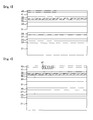
- the threshold currents and voltages of the samples at 20 °C are shown in Figs. 8 and 9 , respectively.
- the sample having the nano patterns with a diameter of 200 nm had a threshold current of 200 mA and a threshold voltage of 26 V.
- the reference sample having a length of 600 ⁇ m had a threshold current of 185 mA and a threshold voltage of 24 V.
- the wavelength of these samples was 401 nm.
- Fig. 10 shows a wavelength change of samples having a length of 600 ⁇ m depending on a temperature.
- a considerably large number of light emitting spectra of the samples according to the embodiment of the present invention appeared in the vicinity of a threshold, but became a single mode at 1.1 times of the threshold.
- the reference sample light emitting spectra did not become a single mode at about 1.1 times of the threshold, and 3 to 10 wavelengths appeared.
- the wavelength showing the maximum intensity was selected as a peak wavelength.
- the spectra were measured using a spectroscope with a resolution of 0.02 nm.
- a wavelength increase depending on temperature was 0.05 nm/°C in case of the sample having the nano patterns with a diameter of 200 nm, and 0.24 nm/°C in case of the reference sample.
- the wavelength increases of all the samples depending on temperature were shown smaller than that of the reference sample.
- the sample having a resonator length closest to 2 ⁇ /n has the smallest wavelength increase (308 nm ⁇ 346 nm).
- the length of a resonator 100 nm
- the distance between desired periodic patterns is 154 nm, which is the same degree as the aforementioned sample.
- a laser diode of a new structure having column-shaped nano patterns periodically arranged therein.
- such nano patterns can be periodically arranged at a fine pitch, whereby a single mode laser with a short wavelength, for example, in a range of 400 nm can be implemented. Further, an angle made by the periodic arrangement of the nano patterns and a cleavage plane is adjusted, so that a laser wavelength can be controlled.
Abstract
Description
- The present invention relates to a laser diode and a method of fabricating the same, and more particularly, to a laser diode having column-shaped nano patterns and a method of fabricating the laser diode.
- Distributed feedback (DFB) laser (or, distributed Bragg reflector laser or Bragg reflector laser) is used in optical communications or the like, in which a wavelength range is extremely limited. A conventional DFB laser diode has a layer having a periodically concavo-convex portion, e.g., a concavo-convex portion with a stripe shape, formed along an active layer and reflects light on the layer, thereby implementing a single mode laser.
- Such a laser diode may be fabricated by stopping crystal growth of a semiconductor layer, forming a concavo-convex portion thereon, and then, growing the semiconductor layer again. However, since in order to form the concavo-convex portion in the laser diode, the semiconductor layer should be grown again after stopping the initial crystal growth of the semiconductor layer and then forming the concavo-convex portion, the semiconductor layers cannot be continuously grown, and therefore, the process of growing semiconductor layers may be complicated.
- Alternatively, a laser diode may be fabricated by forming a concavo-convex portion on a surface of a semiconductor layer which has been completely grown. A technique for forming a concavo-convex portion on a surface of an InP-based semiconductor layer has been disclosed by Kennedy et al. (see Extended Abstracts of the 2006 International Conference on Solid State Devices and Materials, 2006, B-3-6, p262-263).
- Studies on a DFB (or, DBR or DR) laser diode have been continuously required. Particularly, studies on a single mode DFB laser having a wavelength of about 400 nm have been continuously required.
- An object of the present invention is to provide a laser diode with a new structure, particularly a DFB (or, DBR or DR) laser diode having new periodic patterns, and a method of fabricating the laser diode.
- Another object of the present invention is to provide a laser diode, in which a wavelength of a laser can be changed depending on a direction of a cleavage plane, and a method of fabricating the laser diode.
- According to an aspect of the present invention for achieving the objects, there is provided a laser diode having nano patterns. The laser diode has a substrate. A first conductive-type clad layer is disposed over the substrate, and a second conductive-type clad layer is disposed over the first conductive-type clad layer. An active layer is interposed between the first and second conductive-type clad layers. Column-shaped nano patterns are periodically arranged at a surface of the second conductive-type clad layer.
- Here, the column-shaped "nano patterns" means a column-shaped patterns, each of which has a cross sectional area below 1 µm2. Such nano patterns are arranged at the surface of the second conductive-type clad layer, thereby implementing a single mode laser such as a distributed feedback laser diode. The terms "first conductive-type" and "second conductive-type" mean conductive types relative to each other, and mean n-type and p-type or p-type and n-type, respectively.
- The nano patterns may be formed by partially etching the second conductive-type clad layer. For example, the nano patterns may be formed by forming a second conductive-type contact layer on the second conductive-type clad layer and partially etching the second conductive-type clad layer through the second conductive-type contact layer. Thus, the nano patterns are formed by patterning the semiconductor layers after the crystal growth of semiconductor layers is completed. Accordingly, the semiconductor layers can be continuously grown.
- Meanwhile, the nano patterns may have a vertical cross section formed in the shape of a polygon or circle. Particularly, the respective nano patterns may be formed in a circular-column shape having a diameter.
- In addition, the nano patterns may be spaced apart from one another at the same interval as the diameter. Therefore, the nano patterns are arranged in a hive shape, and adjacent three of the nano patterns define a regular triangle. The respective nano patterns may have a diameter of 100 to 250 nm.
- Meanwhile, the laser diode may have cleavage mirrors formed at both opposite side surfaces of the laser diode. The cleavage mirrors may be formed at both side surfaces of the semiconductor layers along cleavage planes of the substrate. The cleavage planes of the substrate, i.e., the cleavage mirrors may be parallel with any one side of a regular triangle defined by the nano patterns adjacent to each other. The present invention is not limited thereto, but the cleavage mirrors may make an angle of intersection with all sides of a regular triangle defined by the nano patterns adjacent to each other. The wavelength of a radiated laser can be controlled by adjusting the angle made by one side of the regular triangle and the cleavage mirror.
- In some embodiments of the present invention, the respective nano patterns may be formed in a protruding column shape, and a second conductive-type contact layer may be provided on an upper side of the respective nano patterns. Alternatively, the laser diode may further comprise a second conductive-type contact layer formed on the second conductive-type clad layer, and the nano patterns may be recessed portions, which are formed in the second conductive-type clad layer by passing through the second conductive-type contact layer. At this time, the recessed portion may have a column shape.
- In some embodiments of the present invention, the laser diode may be a distributed feedback laser diode, a distributed Bragg reflector laser diode or a Bragg reflector laser diode.
- According to another aspect of the present invention, there is provided a method of fabricating a laser diode, which comprises the step of forming semiconductor layers with a laminated structure having a first conductive-type clad layer, an active layer and a second conductive-type clad layer formed on a substrate. Thereafter, the second conductive-type clad layer is partially etched, thereby forming column-shaped nano patterns spaced apart from one another.
- The nano patterns may be formed using a nano lithography technique, particularly a nano imprint technique. Since the nano patterns can be formed throughout the entire surface of a large-sized substrate such as a two-inch substrate, the nano imprint technique is suitable for mass-production of laser diodes.
- Meanwhile, the method may further comprise the step of forming a second conductive-type contact layer on top of the second conductive-type clad layer before partially etching the second conductive-type clad layer.
- In addition, before or after the nano patterns are formed, a mesa may be formed by etching the second conductive-type clad layer, the active layer and the first conductive-type clad layer. At this time, a first conductive-type contact layer for forming a first electrode is exposed. Meanwhile, a ridge may be formed by partially etching the second conductive-type clad layer along both sides of a region where the nano patterns will be positioned. The refractive index of the regions, where the second conductive-type clad layer is partially etched, is decreased, and the ridge has a relatively large refractive index, whereby light is concentrated on the ridge.
-
-
Fig. 1 is a schematic perspective view of a laser diode according to an embodiment of the present invention; -
Fig. 2 is a detailed sectional view of the laser diode shown inFig. 1 according to the embodiment of the present invention; -
Figs. 3 to 6 are sectional views illustrating a method of fabricating a laser diode according to an embodiment of the present invention; -
Fig. 7 is a schematic plan view illustrating samples fabricated according to an embodiment of the present invention; -
Figs. 8 and9 are graphs respectively showing threshold pulse current and voltage measured at 20 °C of various samples, each of which has a laser length L of 600 µm; and -
Fig. 10 is a graph showing a wavelength increase of various samples, each of which has a laser length L of 600 µm, depending on a temperature. - Hereinafter, preferred embodiments of the present invention will be described in detail with reference to the accompanying drawings. The following embodiments are provided only for illustrative purposes so that those skilled in the art can fully understand the spirit of the present invention. Therefore, the present invention is not limited to the following embodiments but may be implemented in other forms. In the drawings, the widths, lengths, thicknesses and the like of elements may be exaggerated for convenience of illustration. Like reference numerals indicate like elements throughout the specification and drawings.
-
Fig. 1 is a schematic perspective view of a laser diode according to an embodiment of the present invention, andFig. 2 is a detailed sectional view of the laser diode shown inFig. 1 . - Referring to
Figs. 1 and 2 , the laser diode comprises asubstrate 21, a first conductive-type cladlayer 35, an active layer, a second conductive-type cladlayer 41, andnano patterns 42 located at a surface of the second conductive-type cladlayer 41. In addition, a first conductive-type contact layer 33 may be interposed between thesubstrate 21 and the first conductive-type cladlayer 35, and a second conductive-type contact layer 43 may be disposed on the second conductive-type cladlayer 41. - The
substrate 21 is not particularly limited if it is a substrate suitable for growing semiconductor layers. Thesubstrate 21 may be a GaN, SiC or sapphire substrate. In this embodiment, it will be described that thesubstrate 21 is a sapphire substrate. - The first and second conductive-type clad
layers substrate 21, and theactive layer 37 is interposed between the first and second conductive-type cladlayers carrier blocking layer 39 may be interposed between the second cladlayer 41 and theactive layer 37. - In this embodiment, the first conductive-type clad
layer 35 may be formed, for example, to have a single-layered structure of n-type AlGaN or a multi-layered structure in which n-type AlGaN and n-type GaN are repeatedly formed. Particularly, the first conductive-type cladlayer 35 may be formed to have a superlattice layer of n-type AlGaN/GaN. The second conductive-type cladlayer 41 may be formed to have a single-layered structure of p-type AlGaN or a multi-layered structure in which AlGaN and GaN are repeatedly formed. Particularly, the second conductive-type cladlayer 41 may be formed to have a superlattice structure of p-type AlGaN/GaN. Theactive layer 37. may be formed to have a single or multiple quantum well structure. For example, theactive layer 37 may be formed to have a multiple quantum well structure in which InGaN well layers and GaN barrier layers are alternately laminated. In addition, thecarrier blocking layer 39 may be formed of p-type AlGaN. Thecarrier blocking layer 39 has a bandgap relatively wider than the second conductive-type cladlayer 41, and therefore, the composition ratio of A1 in thecarrier blocking layer 39 is relatively greater than that of Al in the second conductive-type cladlayer 41. In addition, the first conductive-type contact layer 33 may be formed of n-type GaN, and the second conductive-type contact layer 43 may be formed of p-type GaN. - Meanwhile, the
nano patterns 42 positioned at the surface of the second conductive-type cladlayer 41 may have a column shape, e.g., a polygonal or circular column shape, particularly a circular column shape. Such a circular column shape has a diameter. Thenano patterns 42 are periodically arranged on the surface of the second conductive-type cladlayer 41. - Particularly, the circular-column-shaped nano patterns may be arranged at the same interval as the diameter of the nano patterns, so that adjacent three nano patterns define a regular triangle.
- The periodic interval between the nano patterns may be obtained by wavelength λ/p/refractive index n (e.g., λ = 400 nm, p = 0.5, 1, 2, ..., and n = 2.6). Here, the wavelength λ is a wavelength of a required laser, and p denotes that the periodic interval between the nano patterns is a half times, one times, two times, or the like, of the wavelength. When p = 0.5 and 1, a periodic interval between the nano patterns is 308 nm and 154 nm, respectively.
- Meanwhile, the
substrate 21 may have cleavage planes formed on both side surfaces opposite to each other in a direction of length L of thesubstrate 21. Each of the cleavage planes is parallel with a cleavage mirror, which is formed by cutting theclad layers active layer 35 along the cleavage plane. The wavelength radiated from the laser diode can be adjusted depending on an angle made by the cleavage plane, i.e., the cleavage mirror, and the arrangement direction of the nano patterns. For example, the cleavage mirrors may be parallel with any one side of a regular triangle defined by adjacent nano patterns, or make an angle of intersection with all sides of the regular triangle. - The
nano patterns 42 may be formed by etching the second conductive-type contact layer 43 and the second conductive-type cladlayer 41 together. For example, thenano patterns 42 may be protruding columns including the second conductive-type contact layer 43 and the second conductive-type cladlayer 41, or recessed portions surrounded by the second conductive-type contact layer 43 and the second conductive-type cladlayer 41. - The
nano patterns 42 may be formed at a surface of a ridge of the second conductive-type cladlayer 41, which is formed along the direction of the length L, and the second conductive-type cladlayer 41 in both sides of the ridge may have a thickness relatively smaller than the ridge. The shape of the ridge causes a refractive index difference, thereby making light generated in the active layer be concentrated on the ridge having a relatively large refractive index. InFig. 1 , the width of the ridge is designated by W2. The first conductive-type cladlayer 35, theactive layer 37 and the second conductive-type cladlayer 41 may form a mesa as shown inFigs. 1 and 2 . InFig. 1 , the width of the mesa is designated by W1. - Meanwhile, the first conductive-
type contact layer 33 may be exposed at one or both sides of the mesa. Afirst electrode 49 may be formed on the exposed first conductive-type contact layer 33, and asecond electrode 47 may be formed on thenano patterns 42. An insulatinglayer 45 may cover the first conductive-type contact layer 33, the mesa and the ridge. The insulatinglayer 45 has openings that expose the first and second conductive-type contact layers 33 and 43, and the first and second electrodes may be in electric contact with the contact layers 33 and 43 through the openings, respectively. InFig. 2 , the region at which thesecond electrode 47 is in contact with thesecond contact layer 43, i.e., the opening that exposes the second conductive-type contact layer 43 has a width designated by W3. - In the meantime, buffer layers 23 and 25 and undoped GaN layers 27 and 31 may be interposed between the first conductive-
type contact layer 33 and thesubstrate 21. Adefect prevention layer 29 may be interposed between theundoped layers buffer layer 23 may be formed of SiN, and thebuffer layer 25 may be formed of A1N, GaN or AlGaN. The buffer layers and the undoped GaN layers are employed to reduce defects produced in the semiconductors formed on top thereof. - Although it has been described in this embodiment that the first conductive-
type contact layer 33 is a material layer separate from the first conductive-type cladlayer 35, the first conductive-type contact layer 33 may be the same material layer as the first conductive-type cladlayer 35. That is, the first conductive-type contact layer 33 may be a portion of the first conductive-type cladlayer 35. - According to this embodiment, the column-shaped nano patterns are periodically arranged at the surface of the second conductive-type clad
layer 41, particularly at the surface of the ridge thereof, thereby providing a distributed feedback laser (or, DBR or BR laser) diode. Particularly, a single mode laser in a range of about 400 nm can be implemented using AlInGaN-based compound semiconductor layers. -
Figs. 3 to 6 are sectional views illustrating a method of fabricating a laser diode according to an embodiment of the present invention. - Referring to
Fig. 3 , afirst buffer layer 23 and asecond buffer layer 25 are formed on asubstrate 21. Thesubstrate 21 is not particularly limited but may be, for example, a GaN, SiC or sapphire substrate. Thefirst buffer layer 23 may be formed of SiN using SiH4 and ammonia as a source gas. In addition, thefirst buffer layer 23 may be formed of GaN, AlN or AlGaN by a metal organic chemical vapor deposition (MOCVD) technique. Thefirst buffer layer 23 is a layer for reducing defects, which may be omitted. - A first
undoped layer 27, adefect prevention layer 29 and a secondundoped layer 31 are sequentially formed on thesecond buffer layer 25. The first and secondundoped layers layers defect prevention layer 29 may be formed of SiN and is used to prevent a defect such as dislocation from being transferred from a first undoped layer to a layer formed on the first undoped layer. Such adefect prevention layer 29 may be omitted. - A first conductive-
type contact layer 33 is formed on the secondundoped layer 31. The first conductive-type contact layer 33 may be formed of, for example, n-type GaN. When thesubstrate 21 is non-conductive like sapphire, the first conductive-type contact layer 33 is required to be in contact with a first electrode 49 (seeFig. 1 ). - A first conductive-type clad
layer 35, anactive layer 37, acarrier blocking layer 39 and a second conductive-type cladlayer 41 are formed on the first conductive-type contact layer 33. The first conductive-type cladlayer 35 may be formed to have, for example, a single-layered structure of n-type AlGaN, a multi-layered structure of n-type AlGaN/GaN, or a superlattice structure of n-type AlGaN/GaN. The second conductive-type cladlayer 41 may be formed to have, for example, a single-layered structure of p-type AlGaN, a multi-layered structure of p-type AlGaN/GaN, or a superlattice structure of p-type AlGaN/GaN. Theactive layer 37 may be formed to have, for example, a single quantum well structure of InGaN or a multiple quantum well structure of InGaN/GaN. Thecarrier blocking layer 39 is formed of a material having a bandgap relatively wider than the second conductive-type cladlayer 41. Thecarrier blocking layer 39 may be formed of the same conductive-type material as the second conductive-type cladlayer 41, e.g., AlGaN. - Meanwhile, a second conductive-
type contact layer 43 is formed on the second conductive-type cladlayer 41. The second conductive-type contact layer 43 may be formed of, for example, p-type GaN, and heat treatment may be performed to activate impurities. - Referring to
Fig. 4 , column-shapednano patterns 42 are formed by partially etching the second conductive-type cladlayer 41 and the second conductive-type contact layer 43. Thenano patterns 42, which have a dimension of below 1 µm, may be formed by a nano lithography technique, e.g., a nano imprint technique. Before thelayers type contact layer 43. - The
nano patterns 42 cannot reflect light if the height thereof is too small, whereas theactive layer 37 may be exposed if the height of thenano patterns 42 is too large. Therefore, thenano patterns 42 are formed by partially etching the second conductive-type cladlayer 41 so that theactive layer 37 is not exposed. Thenano patterns 42 are formed to have a height so that light can be reflected. - In addition, the nano patterns may be protruding columns, but without being limited thereto, may be recessed portions. The nano patterns are formed to be roughly arranged at the same interval.
- Referring to
Fig. 5 , a mesa is formed by sequentially etching the second conductive-type contact layer 43, the second conductive-type cladlayer 41, thecarrier blocking layer 39, theactive layer 37 and the first conductive-type cladlayer 35 by a photolithography and etching technique, and a portion of thefirst contact layer 33 is then exposed. - Subsequently, a ridge positioned at a central portion of the mesa is formed by etching the second conductive-
type contact layer 43 and the second conductive-type cladlayer 41, which are positioned in an upper portion of the mesa. At this time, the second conductive-type cladlayer 41 is partially etched, thereby preventing a top surface of theactive layer 37 from being exposed. The process of forming the ridge and the mesa is performed so that thenano patterns 42 remain on the surface of the ridge. As the height of the ridge is relatively larger than that of thenano patterns 42, a refractive index difference between the ridge and its periphery can be increased. - Referring to
Fig. 6 , an insulatinglayer 45 is formed on top of thesubstrate 21 having the ridge and mesa formed thereon and then patterned, thereby forming anopening 47a that exposes the ridge and anopening 49a that exposes the first conductive-type contact layer 33. Theopenings layer 45 by a photolithography and etching technique. - Subsequently, first and
second electrodes 49 and 47 (seeFig. 1 ) for respectively covering theopenings first electrode 49 may be formed of Ti/Al, and thesecond electrode 47 may be formed of Ni/Au. These electrodes may be formed by a lift-off process. Accordingly, the laser diode ofFigs. 1 and 2 is completed. - According to this embodiment, column-shaped nano patterns may be formed using a nano imprint technique, and such nano patterns may be formed to be arranged at a dense interval.
- Although it has been described in this embodiment that the second conductive-type clad
layer 35 is formed on the first conductive-type contact layer 33, the first conductive-type contact layer 33 may be omitted. In this case, a portion of the first conductive-type cladlayer 35 may be exposed while the mesa is formed, and thefirst electrode 49 may be formed on the exposed first conductive-type cladlayer 35. -
Fig. 7 is a schematic plan view illustrating samples used in an experiment. - Referring to
Figs. 3 and7 , a two-inch sapphire substrate 21 was first annealed at 1150 °C for 10 minutes, and anSiN buffer layer 23 was then formed at 500 °C using SiH4 and ammonia. Thereafter, aGaN buffer layer 25 was formed to a thickness of 20 nm, and anundoped GaN layer 27 was grown to a thickness of 3 µm at 1050 °C. Subsequently, a SiNdefect prevention layer 29 was grown again, and anundoped GaN layer 31 was then grown to a thickness of 3 µm. A first conductive-type contact layer 33 was grown on theundoped GaN layer 31 to a thickness of 2 µm using n-type GaN, and n-type Al0.1Ga0.9N of a thickness of 2 nm and n-type GaN of a thickness of 2 nm were repeatedly formed 150 times, thereby forming a first conductive-type cladlayer 35. Thereafter, In0.05Ga0.95N of a thickness of 2 nm and GaN of a thickness of 10 nm were repeatedly formed five times at 700 °C, thereby forming anactive layer 37 of a multiple quantum well structure. Subsequently, acarrier blocking layer 37 of p-type Al0.3Ga0.7N was grown to a thickness of 20 nm at 1020 °C, and p-type Al0.15Ga0.85N of a thickness of 2 nm and GaN of a thickness of 2 nm were repeatedly grown 150 times, thereby forming a second conductive-type cladlayer 41. Then, a second conductive-type contact layer 43 of p-type GaN was formed to a thickness of 20 nm on the second conductive-type cladlayer 41. Thereafter, the substrate was heat-treated at 700 °C for ten minutes so as to activate p-type impurities. - Referring to
Figs. 4 and7 , an SiO2 layer was formed to a thickness of 50 nm on the second conductive-type contact layer 43. Then, the substrate is divided into four regions as shown inFig. 7 , and a mask is formed so that circular columns were formed in each region to have a diameter of 100 nm in region I, 150 nm in region II, 200 nm in region III, or 250 nm in region IV at the same interval as the diameter of the circular columns. The mask was formed using a nano imprint technique. Thereafter, the SiO2 layer was etched by performing reactive ion etching (RIE) for 2 minutes using CF4, and the GaN or AlGaN/GaN layer was then etched at 100 W for 8 minutes using BCl3. Then, the mask was removed by performing RIE using O2, and the SiO2 layer was removed by performing RIE using CF4 (also, the layer can be removed by using HF). It can be seen that nano patterns having a height of 300 nm was formed with AFM. - Referring to
Figs. 5 and7 , a mesa is formed by performing an etching process to a depth of 2 µm using a photolithography and etching technique so that a width of 100 µm (W1 inFig. 1 ) remains in each of the regions. At this time, the etching was performed using BCl3+Cl2. In addition, a ridge was formed by performing 600 nm etching so that a width of 50 µm remains. - Referring to
Figs. 6 and7 , an SiO2 insulating layer 45 was formed to a thickness of 100 nm, andopenings opening 47a was formed to have a width of 2 µm. Subsequently, as shown inFig. 2 , afirst electrode 49 and asecond electrode 47 were formed of Ti/Au and Ni/Au to thicknesses of 50 nm and 10 nm by a lift-off technique, respectively. Au having a thickness of 1 µm was deposited on each of the first and second electrodes. At this time, thefirst electrode 49 was formed to a width of 100 µm, and thesecond electrode 47 was formed to a width of 50 µm. - Subsequently, the respective samples are separated from the
substrate 21 by cleaving thesubstrate 21. In this case, the cleaving was performed in parallel with a cutting axis C ofFig. 7 so that one side of a regular triangle of the nano patterns is parallel with a cleavage plane of the substrate. Thus, the length of each side of the rectangular triangle is 2 times greater than the diameter of the nano patterns, and the distance between adjacent parallel two sides of the rectangular triangles is 1.73 times greater than the diameter of the nano patterns. Thus, the samples obtained from the respective regions ofFig. 7 are arranged at periods of 173, 260, 346 and 433nm, each of which becomes a resonator length. Therefore, each sample becomes a laser diode in which cleavage mirrors and Bragg reflectors coexist. - Meanwhile, as a reference sample for the samples, a sample was fabricated in the same manner as the aforementioned samples using one region of the
substrate 21 except the nano patterns. The respective samples were fabricated to have different lengths L in a range of 300 µm to 1 mm. - A pulse current having a pulse time of 1 ms and a pulse width of 100 ns was applied to the samples. At this time, the samples having length L of 600 µm were all oscillated. The threshold currents and voltages of the samples at 20 °C are shown in
Figs. 8 and9 , respectively. - Referring to
Figs. 8 and9 , the sample having the nano patterns with a diameter of 200 nm had a threshold current of 200 mA and a threshold voltage of 26 V. The reference sample having a length of 600 µm had a threshold current of 185 mA and a threshold voltage of 24 V. The wavelength of these samples was 401 nm. - Meanwhile, the samples having length L of below 400 µm or over 800 µm were not oscillated. This is because the threshold voltages of these samples exceeded 30 V although the maximum voltage of a pulse transmitter is 30 V.
- In the meantime, light emitting spectra were measured by changing a temperature from 20 to 80 °C.
Fig. 10 shows a wavelength change of samples having a length of 600 µm depending on a temperature. A considerably large number of light emitting spectra of the samples according to the embodiment of the present invention appeared in the vicinity of a threshold, but became a single mode at 1.1 times of the threshold. On the contrary, in the reference sample, light emitting spectra did not become a single mode at about 1.1 times of the threshold, and 3 to 10 wavelengths appeared. Thus, in case of the reference sample, the wavelength showing the maximum intensity was selected as a peak wavelength. The spectra were measured using a spectroscope with a resolution of 0.02 nm. - Referring to
Fig. 10 , a wavelength increase depending on temperature was 0.05 nm/°C in case of the sample having the nano patterns with a diameter of 200 nm, and 0.24 nm/°C in case of the reference sample. The wavelength increases of all the samples depending on temperature were shown smaller than that of the reference sample. - The sample having a resonator length closest to 2λ/n has the smallest wavelength increase (308 nm ≒ 346 nm). However, in case of the sample having the nano patterns of a = 100 nm, the length of a resonator is 173 nm, and the distance between desired periodic patterns is 154 nm, which is the same degree as the aforementioned sample. Here, the wavelength increase of the sample depending on temperature was considerably large. It is estimated that the samples of a = 100 nm were not precisely formed to have a diameter and an interval of 100 nm.
- According to the embodiments of the present invention, there is provided a laser diode of a new structure having column-shaped nano patterns periodically arranged therein. Particularly, such nano patterns can be periodically arranged at a fine pitch, whereby a single mode laser with a short wavelength, for example, in a range of 400 nm can be implemented. Further, an angle made by the periodic arrangement of the nano patterns and a cleavage plane is adjusted, so that a laser wavelength can be controlled.
Claims (16)
- A laser diode, comprising:a substrate;a first conductive-type clad layer disposed above the substrate;a second conductive-type clad layer disposed over the first conductive-type clad layer;an active layer interposed between the first and second clad layers; andcolumn-shaped nano patterns periodically arranged at a surface of the second conductive-type clad layer.
- The laser diode as claimed in claim 1, wherein the nano patterns are formed by partially etching the second conductive-type clad layer.
- The laser diode as claimed in claim 1, wherein the respective nano patterns are formed in a circular-column shape having a diameter.
- The laser diode as claimed in claim 3, wherein the nano patterns are spaced apart from one another at the same interval as the diameter.
- The laser diode as claimed in claim 4, wherein the respective nano patterns have a diameter of 100 to 250 nm.
- The laser diode as claimed in claim 4, wherein cleavage mirrors are respectively formed at both opposite side surfaces of the laser diode, and each of the cleavage mirrors is parallel with any one side of a regular triangle defined by the nano patterns adjacent to one another.
- The laser diode as claimed in claim 4, wherein cleavage mirrors are respectively formed at both opposite side surfaces of the laser diode, and each of the cleavage mirrors make an angle of intersection with all sides of a regular triangle defined by the nano patterns adjacent to one another.
- The laser diode as claimed in claim 1, wherein the respective nano patterns are formed in a protruding column shape, and a second conductive-type contact layer is provided on an upper side of the respective nano patterns.
- The laser diode as claimed in claim 1, further comprising a second conductive-type contact layer formed on the second conductive-type clad layer, wherein the nano patterns are recessed portions, which are formed in the second conductive-type clad layer through the second conductive-type contact layer.
- The laser diode as claimed in claim 1, wherein the laser diode is any one of a distributed feedback laser diode, a distributed Bragg reflector laser diode and a Bragg reflector laser diode.
- A method of fabricating a laser diode, comprising:forming semiconductor layers with a laminated structure having a first conductive-type clad layer, an active layer and a second conductive-type clad layer formed on a substrate; andforming column-shaped nano patterns spaced apart from one another by partially etching the second conductive-type clad layer.
- The method as claimed in claim 11, wherein the nano patterns are formed using a nano imprint technique.
- The method as claimed in claim 11, further comprising:forming a second conductive-type contact layer on the second conductive-type clad layer before partially etching the second conductive-type clad layer.
- The method as claimed in claim 11, wherein the nano patterns are periodically arranged so that adjacent three of the nano patterns define a regular triangle.
- The method as claimed in claim 14, wherein cleavage mirrors are respectively formed at both opposite side surfaces of the laser diode by cleaving the substrate, and the cleavage mirrors are parallel with any one side of a regular triangle defined by adjacent three of the nano patterns.
- The method as claimed in claim 14, wherein cleavage mirrors are respectively formed at both opposite side surfaces of the laser diode by cleaving the substrate, and the cleavage mirrors make an angle of intersection with all sides of a regular triangle defined by adjacent three of the nano patterns.
Applications Claiming Priority (1)
| Application Number | Priority Date | Filing Date | Title |
|---|---|---|---|
| KR1020070101262A KR101423721B1 (en) | 2007-10-09 | 2007-10-09 | Laser diode having nano patterns thereon and method of fabricating the same |
Publications (3)
| Publication Number | Publication Date |
|---|---|
| EP2048754A2 true EP2048754A2 (en) | 2009-04-15 |
| EP2048754A3 EP2048754A3 (en) | 2009-09-16 |
| EP2048754B1 EP2048754B1 (en) | 2015-09-09 |
Family
ID=39798216
Family Applications (1)
| Application Number | Title | Priority Date | Filing Date |
|---|---|---|---|
| EP08012762.4A Expired - Fee Related EP2048754B1 (en) | 2007-10-09 | 2008-07-15 | Laser diode having nano patterns and method of fabricating the same |
Country Status (5)
| Country | Link |
|---|---|
| US (2) | US7760784B2 (en) |
| EP (1) | EP2048754B1 (en) |
| JP (1) | JP5383109B2 (en) |
| KR (1) | KR101423721B1 (en) |
| TW (1) | TWI379479B (en) |
Families Citing this family (5)
| Publication number | Priority date | Publication date | Assignee | Title |
|---|---|---|---|---|
| JP2009088425A (en) * | 2007-10-03 | 2009-04-23 | Sony Corp | Semiconductor laser, and manufacturing method therefor |
| KR101064006B1 (en) * | 2009-03-03 | 2011-09-08 | 엘지이노텍 주식회사 | Light emitting element |
| KR100999684B1 (en) * | 2009-10-21 | 2010-12-08 | 엘지이노텍 주식회사 | Light emitting device and method for fabricating the same |
| TWI492416B (en) * | 2010-03-24 | 2015-07-11 | Hon Hai Prec Ind Co Ltd | Light emitting diode chip and making method thereof |
| US10008828B1 (en) | 2016-12-28 | 2018-06-26 | Intel Corporation | High-efficiency semiconductor laser |
Family Cites Families (22)
| Publication number | Priority date | Publication date | Assignee | Title |
|---|---|---|---|---|
| FR2734097B1 (en) * | 1995-05-12 | 1997-06-06 | Thomson Csf | SEMICONDUCTOR LASER |
| US5955749A (en) * | 1996-12-02 | 1999-09-21 | Massachusetts Institute Of Technology | Light emitting device utilizing a periodic dielectric structure |
| JPH10261838A (en) * | 1997-03-19 | 1998-09-29 | Sharp Corp | Gallium nitride semiconductor light-emitting element and semiconductor laser beam source device |
| KR100421147B1 (en) * | 1997-06-19 | 2004-05-31 | 삼성전자주식회사 | Semiconductor laser device having two-dimensional photonic band gap structure and fabricating method thereof |
| DE60129286T2 (en) * | 2000-12-27 | 2007-11-22 | Nippon Telegraph And Telephone Corp. | Photonic crystal waveguide |
| US6674778B1 (en) | 2002-01-09 | 2004-01-06 | Sandia Corporation | Electrically pumped edge-emitting photonic bandgap semiconductor laser |
| JP3613348B2 (en) * | 2002-02-08 | 2005-01-26 | 松下電器産業株式会社 | Semiconductor light emitting device and manufacturing method thereof |
| JP2004030964A (en) * | 2002-06-21 | 2004-01-29 | Seiko Epson Corp | Light emitting device, device for optical communication, and optical communication system |
| FR2842037B1 (en) * | 2002-07-08 | 2004-10-01 | Cit Alcatel | DFB LASER WITH DISTRIBUTED REFLECTOR WITH PROHIBITED PHOTONIC BAND |
| JP2004172506A (en) * | 2002-11-22 | 2004-06-17 | Sony Corp | Semiconductor laser device |
| US7211831B2 (en) * | 2003-04-15 | 2007-05-01 | Luminus Devices, Inc. | Light emitting device with patterned surfaces |
| JP4761426B2 (en) * | 2003-07-25 | 2011-08-31 | 三菱電機株式会社 | Optical device and semiconductor laser oscillator |
| JP2005109102A (en) * | 2003-09-30 | 2005-04-21 | Mitsubishi Electric Corp | Monolithic semiconductor laser and manufacturing method thereof |
| JP4479214B2 (en) | 2003-10-22 | 2010-06-09 | ソニー株式会社 | Semiconductor laser |
| US7250635B2 (en) * | 2004-02-06 | 2007-07-31 | Dicon Fiberoptics, Inc. | Light emitting system with high extraction efficency |
| US7298949B2 (en) * | 2004-02-12 | 2007-11-20 | Sioptical, Inc. | SOI-based photonic bandgap devices |
| KR100619751B1 (en) * | 2004-10-23 | 2006-09-13 | 엘지전자 주식회사 | Shading coil type single-phase hybride induction motor |
| KR100672077B1 (en) * | 2004-11-05 | 2007-01-19 | 광주과학기술원 | Method of manufacturing light emitting device |
| JP2006165309A (en) * | 2004-12-08 | 2006-06-22 | Sumitomo Electric Ind Ltd | Semiconductor laser element |
| US7483466B2 (en) * | 2005-04-28 | 2009-01-27 | Canon Kabushiki Kaisha | Vertical cavity surface emitting laser device |
| US7499480B2 (en) * | 2006-11-16 | 2009-03-03 | Canon Kabushiki Kaisha | Photonic crystal structure and surface-emitting laser using the same |
| JP2008182110A (en) * | 2007-01-25 | 2008-08-07 | Matsushita Electric Ind Co Ltd | Nitride semiconductor light-emitting device |
-
2007
- 2007-10-09 KR KR1020070101262A patent/KR101423721B1/en active IP Right Grant
-
2008
- 2008-07-15 EP EP08012762.4A patent/EP2048754B1/en not_active Expired - Fee Related
- 2008-07-22 JP JP2008188715A patent/JP5383109B2/en active Active
- 2008-07-29 TW TW097128686A patent/TWI379479B/en active
- 2008-08-05 US US12/185,995 patent/US7760784B2/en active Active
-
2010
- 2010-04-27 US US12/768,073 patent/US8189635B2/en active Active
Non-Patent Citations (1)
| Title |
|---|
| EXTENDED ABSTRACTS OF THE 2006 INTERNATIONAL CONFERENCE ON SOLID STATE DEVICES AND MATERIALS, vol. B-3-6, 2006, pages 262 - 263 |
Also Published As
| Publication number | Publication date |
|---|---|
| JP2009094471A (en) | 2009-04-30 |
| US8189635B2 (en) | 2012-05-29 |
| TW200917604A (en) | 2009-04-16 |
| KR20090036217A (en) | 2009-04-14 |
| EP2048754B1 (en) | 2015-09-09 |
| US7760784B2 (en) | 2010-07-20 |
| US20090092165A1 (en) | 2009-04-09 |
| KR101423721B1 (en) | 2014-07-31 |
| TWI379479B (en) | 2012-12-11 |
| US20100208762A1 (en) | 2010-08-19 |
| EP2048754A3 (en) | 2009-09-16 |
| JP5383109B2 (en) | 2014-01-08 |
Similar Documents
| Publication | Publication Date | Title |
|---|---|---|
| US5701321A (en) | Semiconductor laser producing short wavelength light | |
| US8274088B2 (en) | Surface-emitting laser element, fabrication method thereof, surface-emitting laser array, and fabrication method thereof | |
| US20060060833A1 (en) | Radiation-emitting optoelectronic component with a quantum well structure and method for producing it | |
| US20040206969A1 (en) | Semiconductor light-emitting device and method for fabricating the same | |
| US6754245B2 (en) | GaN series surface-emitting laser diode having spacer for effective diffusion of holes between p-type electrode and active layer, and method for manufacturing the same | |
| KR100345452B1 (en) | Long-wavelength vertical-cavity surface-emitting laser device having diffusion area in edge of upper mirror and method for forming the same | |
| US6201265B1 (en) | Group III-V type nitride compound semiconductor device and method of manufacturing the same | |
| US8526480B2 (en) | Semiconductor laser device | |
| KR101834572B1 (en) | Nitride semiconductor laser element and method for manufacturing the same | |
| US8189635B2 (en) | Laser diode having nano patterns and method of fabricating the same | |
| US20080130698A1 (en) | Nitride-based semiconductor device and method of fabricating the same | |
| US7666694B2 (en) | Method for manufacturing semiconductor laser device and semiconductor laser device | |
| US8962356B2 (en) | Method of manufacturing photonic crystal and method of manufacturing surface-emitting laser | |
| JP4194844B2 (en) | Semiconductor laser with multiple optically active regions | |
| KR20220140748A (en) | Micro-LED and method for making same | |
| KR20060131652A (en) | Single elog growth transverse p-n junction nitride semiconductor laser | |
| US8183649B2 (en) | Buried aperture nitride light-emitting device | |
| JP2009105184A (en) | Nitride semiconductor laser device and method of producing the same | |
| JP2004134501A (en) | Light emitting device and its manufacturing method | |
| EP0955709A2 (en) | Blue edge emitting laser | |
| DE102023110664A1 (en) | SEMICONDUCTOR LASER AND METHOD FOR PRODUCING THE SAME |
Legal Events
| Date | Code | Title | Description |
|---|---|---|---|
| PUAI | Public reference made under article 153(3) epc to a published international application that has entered the european phase |
Free format text: ORIGINAL CODE: 0009012 |
|
| AK | Designated contracting states |
Kind code of ref document: A2 Designated state(s): AT BE BG CH CY CZ DE DK EE ES FI FR GB GR HR HU IE IS IT LI LT LU LV MC MT NL NO PL PT RO SE SI SK TR |
|
| AX | Request for extension of the european patent |
Extension state: AL BA MK RS |
|
| PUAL | Search report despatched |
Free format text: ORIGINAL CODE: 0009013 |
|
| AK | Designated contracting states |
Kind code of ref document: A3 Designated state(s): AT BE BG CH CY CZ DE DK EE ES FI FR GB GR HR HU IE IS IT LI LT LU LV MC MT NL NO PL PT RO SE SI SK TR |
|
| AX | Request for extension of the european patent |
Extension state: AL BA MK RS |
|
| 17P | Request for examination filed |
Effective date: 20100121 |
|
| AKX | Designation fees paid |
Designated state(s): DE FR GB |
|
| 17Q | First examination report despatched |
Effective date: 20101124 |
|
| RAP1 | Party data changed (applicant data changed or rights of an application transferred) |
Owner name: THE UNIVERSITY OF TOKUSHIMA Owner name: SEOUL VIOSYS CO., LTD |
|
| RIC1 | Information provided on ipc code assigned before grant |
Ipc: H01S 5/02 20060101ALN20150408BHEP Ipc: B82Y 20/00 20110101ALI20150408BHEP Ipc: H01L 33/00 20100101ALN20150408BHEP Ipc: H01S 5/22 20060101ALI20150408BHEP Ipc: H01S 5/12 20060101AFI20150408BHEP |
|
| GRAP | Despatch of communication of intention to grant a patent |
Free format text: ORIGINAL CODE: EPIDOSNIGR1 |
|
| RIC1 | Information provided on ipc code assigned before grant |
Ipc: H01S 5/12 20060101AFI20150508BHEP Ipc: H01L 33/00 20100101ALN20150508BHEP Ipc: B82Y 20/00 20110101ALI20150508BHEP Ipc: H01S 5/22 20060101ALI20150508BHEP Ipc: H01S 5/02 20060101ALN20150508BHEP |
|
| INTG | Intention to grant announced |
Effective date: 20150527 |
|
| GRAS | Grant fee paid |
Free format text: ORIGINAL CODE: EPIDOSNIGR3 |
|
| GRAA | (expected) grant |
Free format text: ORIGINAL CODE: 0009210 |
|
| AK | Designated contracting states |
Kind code of ref document: B1 Designated state(s): DE FR GB |
|
| REG | Reference to a national code |
Ref country code: GB Ref legal event code: FG4D |
|
| REG | Reference to a national code |
Ref country code: DE Ref legal event code: R096 Ref document number: 602008040036 Country of ref document: DE |
|
| REG | Reference to a national code |
Ref country code: DE Ref legal event code: R097 Ref document number: 602008040036 Country of ref document: DE |
|
| REG | Reference to a national code |
Ref country code: FR Ref legal event code: PLFP Year of fee payment: 9 |
|
| PLBE | No opposition filed within time limit |
Free format text: ORIGINAL CODE: 0009261 |
|
| STAA | Information on the status of an ep patent application or granted ep patent |
Free format text: STATUS: NO OPPOSITION FILED WITHIN TIME LIMIT |
|
| 26N | No opposition filed |
Effective date: 20160610 |
|
| REG | Reference to a national code |
Ref country code: FR Ref legal event code: PLFP Year of fee payment: 10 |
|
| REG | Reference to a national code |
Ref country code: FR Ref legal event code: PLFP Year of fee payment: 11 |
|
| PGFP | Annual fee paid to national office [announced via postgrant information from national office to epo] |
Ref country code: FR Payment date: 20210625 Year of fee payment: 14 |
|
| PGFP | Annual fee paid to national office [announced via postgrant information from national office to epo] |
Ref country code: GB Payment date: 20210625 Year of fee payment: 14 |
|
| PGFP | Annual fee paid to national office [announced via postgrant information from national office to epo] |
Ref country code: DE Payment date: 20210622 Year of fee payment: 14 |
|
| REG | Reference to a national code |
Ref country code: DE Ref legal event code: R119 Ref document number: 602008040036 Country of ref document: DE |
|
| GBPC | Gb: european patent ceased through non-payment of renewal fee |
Effective date: 20220715 |
|
| PG25 | Lapsed in a contracting state [announced via postgrant information from national office to epo] |
Ref country code: FR Free format text: LAPSE BECAUSE OF NON-PAYMENT OF DUE FEES Effective date: 20220731 |
|
| PG25 | Lapsed in a contracting state [announced via postgrant information from national office to epo] |
Ref country code: GB Free format text: LAPSE BECAUSE OF NON-PAYMENT OF DUE FEES Effective date: 20220715 Ref country code: DE Free format text: LAPSE BECAUSE OF NON-PAYMENT OF DUE FEES Effective date: 20230201 |