EP2043385A2 - Vibration transducer and manufacturing method therefor - Google Patents
Vibration transducer and manufacturing method therefor Download PDFInfo
- Publication number
- EP2043385A2 EP2043385A2 EP08016986A EP08016986A EP2043385A2 EP 2043385 A2 EP2043385 A2 EP 2043385A2 EP 08016986 A EP08016986 A EP 08016986A EP 08016986 A EP08016986 A EP 08016986A EP 2043385 A2 EP2043385 A2 EP 2043385A2
- Authority
- EP
- European Patent Office
- Prior art keywords
- diaphragm
- plate
- center portion
- vibration transducer
- spacers
- Prior art date
- Legal status (The legal status is an assumption and is not a legal conclusion. Google has not performed a legal analysis and makes no representation as to the accuracy of the status listed.)
- Withdrawn
Links
Images


Classifications
-
- H—ELECTRICITY
- H04—ELECTRIC COMMUNICATION TECHNIQUE
- H04R—LOUDSPEAKERS, MICROPHONES, GRAMOPHONE PICK-UPS OR LIKE ACOUSTIC ELECTROMECHANICAL TRANSDUCERS; DEAF-AID SETS; PUBLIC ADDRESS SYSTEMS
- H04R19/00—Electrostatic transducers
-
- H—ELECTRICITY
- H04—ELECTRIC COMMUNICATION TECHNIQUE
- H04R—LOUDSPEAKERS, MICROPHONES, GRAMOPHONE PICK-UPS OR LIKE ACOUSTIC ELECTROMECHANICAL TRANSDUCERS; DEAF-AID SETS; PUBLIC ADDRESS SYSTEMS
- H04R19/00—Electrostatic transducers
- H04R19/005—Electrostatic transducers using semiconductor materials
-
- H—ELECTRICITY
- H04—ELECTRIC COMMUNICATION TECHNIQUE
- H04R—LOUDSPEAKERS, MICROPHONES, GRAMOPHONE PICK-UPS OR LIKE ACOUSTIC ELECTROMECHANICAL TRANSDUCERS; DEAF-AID SETS; PUBLIC ADDRESS SYSTEMS
- H04R19/00—Electrostatic transducers
- H04R19/01—Electrostatic transducers characterised by the use of electrets
- H04R19/016—Electrostatic transducers characterised by the use of electrets for microphones
-
- H—ELECTRICITY
- H04—ELECTRIC COMMUNICATION TECHNIQUE
- H04R—LOUDSPEAKERS, MICROPHONES, GRAMOPHONE PICK-UPS OR LIKE ACOUSTIC ELECTROMECHANICAL TRANSDUCERS; DEAF-AID SETS; PUBLIC ADDRESS SYSTEMS
- H04R31/00—Apparatus or processes specially adapted for the manufacture of transducers or diaphragms therefor
- H04R31/006—Interconnection of transducer parts
-
- H—ELECTRICITY
- H04—ELECTRIC COMMUNICATION TECHNIQUE
- H04R—LOUDSPEAKERS, MICROPHONES, GRAMOPHONE PICK-UPS OR LIKE ACOUSTIC ELECTROMECHANICAL TRANSDUCERS; DEAF-AID SETS; PUBLIC ADDRESS SYSTEMS
- H04R2201/00—Details of transducers, loudspeakers or microphones covered by H04R1/00 but not provided for in any of its subgroups
- H04R2201/003—Mems transducers or their use
Definitions
- the present invention relates to vibration transducers and in particular to wave transducers such as miniature condenser microphones serving as MEMS sensors.
- the present invention also relates to manufacturing methods of vibration transducers.
- Patent Documents 1, 2, 3 and Non-Patent Document 1 Various types of vibration transducers have been developed and disclosed in various documents such as Patent Documents 1, 2, 3 and Non-Patent Document 1.
- Miniature condenser microphones have been conventionally known as typical types of vibration transducers and have been produced by way of semiconductor device manufacturing processes.
- Condenser microphones are referred to as MEMS microphones (where MEMS stands for Micro Electro Mechanical System).
- MEMS Micro Electro Mechanical System
- a typical example of condenser microphones is constituted of a substrate, a diaphragm, and a plate.
- the diaphragm and plate serving as opposite electrodes, which are distanced from each other, are composed of films deposed on the substrate and are supported above the substrate.
- the electrostatic capacitance between the diaphragm and the plate varies due to the displacement of the diaphragm, and then variations of electrostatic capacitance are converted into electric signals.
- This condenser microphone (or vibration transducer) is designed such that the peripheral portion of the plate joins an insulating film.
- a vibration transducer in a first aspect of the present invention, includes a diaphragm having a conductive property, a plate having a conductive property, which is positioned opposite to the diaphragm, and a plurality of first spacers having pillar shapes which are formed using a deposited film having an insulating property joining the plate and which supports the plate relative to the diaphragm with a gap therebetween, wherein an electrostatic capacitance formed between the diaphragm and the plate is varied when the diaphragm vibrates relative to the plate.
- the first spacers each having a high dielectric constant (higher than that of the air) be each reduced in area in plan view. That is, the plate is supported by the first spacers, which are not formed in ring shapes but are formed in a pillar shape, whereby it is possible to reduce the electrostatic capacitance between the diaphragm and the plate, thus improving the sensitivity.
- the geometric shapes of the first spacers are not necessarily limited to pillar shapes but can also be formed in flat shapes.
- the present invention does not need the support having a structurally closed shape but multiple supports which are formed in any shape for supporting the plate. It may be possible to reduce the parasitic capacitance by forming the plate or the diaphragm by use of an insulating substance in the region in which the diaphragm and the plate is positioned opposite to each other; however, this causes complexity in film structure with respect to at least one of the diaphragm and the plate
- the aforementioned vibration transducer is manufactured in such a way that a plurality of holes are formed in the plate; isotropic etching is performed using the plate as a mask so as to remove a part of the deposited film, thus forming the gap between the plate and the diaphragm; and the first spacers are formed by use of the remaining deposited film. Since the plate is used as the etching mask so as to form the first spacers, it is possible to reduce the total number of masks, thus reducing the manufacturing cost.
- the plate has a plurality of holes which allow an etchant to transmit therethrough in isotropic etching, thus simultaneously forming the first spacers and the gap between the plate and the diaphragm.
- the vibration transducer further includes a substrate and a plurality of second spacers having pillar shapes which are formed using a deposited film having an insulating property and which support the plate relative to the substrate with a gap therebetween, wherein an electrostatic capacitance formed between the diaphragm and the plate is varied when the diaphragm vibrates relative to the plate.
- the second spacers each be reduced in area in plan view. That is, the plate is supported by the second spacers which are formed not in ring shapes but in pillar shapes, whereby it is possible to reduce the electrostatic capacitance between the substrate and the plate, thus improving the sensitivity of the vibration transducer.
- the geometric shapes of the second spacers are not necessarily limited to pillar shapes but can also be formed in flat shapes. The present invention does not need the support having a structurally closed shape but multiple supports which are formed in any shapes for supporting the plate.
- the vibration transducer is manufactured in such a way that a plurality of holes is formed in the plate; isotropic etching is performed using the plate as a mask so as to remove a part of the deposited film, thus forming the gap between the plate and the substrate; and the second spacers are formed using the remaining of the deposited film. Since the plate is used as an etching mask for use in the formation of the second spacers, it is possible to reduce the number of masks, thus reducing the manufacturing cost.
- the plate has a plurality of holes allowing an etchant to transmit therethrough in isotropic etching, thus simultaneously forming the second spacers and the gap between the plate and the substrate.
- the distance between the center and the external end of the plate is smaller than the distance between the center and the external end of the diaphragm.
- the electrostatic capacitance between the diaphragm and the plate varies very little or is not varied substantially.
- the external portion of the diaphragm is fixed to its upper or lower film, it causes a very small amplitude of vibration.
- the vibration transducer is designed such that the distance between the center and the external end of the plate becomes smaller than the distance between the center and the external end of the diaphragm, thus inhibiting the external portion of the diaphragm from being positioned opposite to the plate.
- the plate and the diaphragm are both formed in a circular shape or when they have no recess in the outlines thereof, it is required that the external end of the plate is positioned inwardly of the external end of the diaphragm.
- the plate and the diaphragm are both formed in a circular shape or when they have no recess in the outlines thereof, it is required that the shortest distance between the center and the external end of the plate be shorter than the shortest distance between the center and the external end of the diaphragm. Even when the plate is formed in a circular shape or does not have a recess in the outline thereof and even when the diaphragm has recesses in the outline thereof, it is required that the shortest distance between the center and the external end of the plate be shorter than the shortest distance between the center and the external end of the diaphragm.
- the aforementioned structure of the vibration transducer is capable of reducing the parasitic capacitance between the diaphragm and the plate, thus improving the sensitivity.
- the vibration transducer further includes a plurality of third spacers having pillar shapes which are formed using a deposited film having an insulating property which joins the substrate and the diaphragm and which supports the diaphragm relative to the substrate with a gap therebetween.
- a parasitic capacitance is formed between the diaphragm and the substrate in the region in which they are positioned opposite to each other via the third spacers, it is preferable that the area of the third spacer (whose dielectric constant is higher than that of the air) be as small as possible.
- Each of the third spacers is not formed in a ring shape but in a pillar shape, whereby the diaphragm is supported by multiple third spacers; thus, it is possible to reduce the parasitic capacitance between the substrate and the diaphragm, thus improving the sensitivity.
- the geometric shapes of the third spacers are not necessarily limited to pillar shapes but can be formed in flat shapes. It is required that the third spacer not be formed in a closed wall structure, but a plurality of third spacers be formed in any shape for supporting the diaphragm.
- the plate is constituted of a center portion and a plurality of arms which are extended outwardly in a radial direction from the center portion, whereby the diaphragm is not positioned opposite to the plate at the arms and in the cutout regions between the arms. Due to the formation of the arms which are extended outwardly in a radial direction from the center portion of the plate, it is possible to reduce the parasitic capacitance formed between the diaphragm and the plate.
- a vibration transducer in a second aspect of the present invention, includes a substrate, a diaphragm having a conductive property which is constituted of a center portion and a plurality of arms extended outwardly in a radial direction from the center portion, a plate having a conductive property which is constituted of a center portion, which is positioned opposite to the center portion of the diaphragm, and a plurality of arms extended outwardly in a radial direction from the center portion thereof, a plurality of plate supports for supporting the plate, and a plurality of diaphragm supports having pillar shapes which are positioned between the cutouts formed between the arms of the plate and which are positioned outwardly of the plate supports in the radial direction of the plate so as to support the diaphragm.
- each arm of the diaphragm in the circumferential direction of the diaphragm becomes shortest in the intermediate region between the center portion and the joint portion at which each arm joins each diaphragm support but becomes longer in proximity to the joint portion.
- an electrostatic capacitance formed between the diaphragm and the plate is varied when the diaphragm vibrates relative to the plate.
- the arms of the diaphragm are positioned alternately with the arms of the plate in plan view, wherein the distance between the plate supports which are positioned opposite to each other so as to support the plate is shorter than the distance between the diaphragm supports which are positioned opposite to each other so as to support the diaphragm. That is, the diaphragm supports which join the arms of the diaphragm and the substrate are positioned between the plate supports in the circumferential direction of the plate and are positioned externally of the plate supports in the radial direction of the plate. This increases the rigidity of the plate to be relatively higher than the rigidity of the diaphragm.
- the joint strength between the arms of the diaphragm and the diaphragm supports increase as the joint areas therebetween increase; thus, it is possible to increase the durability of the vibration transducer.
- the joint areas are increased by increasing the lengths of the diaphragm supports in the radial direction of the diaphragm, the rigidity of the diaphragm is not changed (so that the sensitivity is not increased) irrespective of the substantial length of the diaphragm between the diaphragm supports, whereas the vibration transducer may be increased in size.
- the widths of the arms of the diaphragm in its circumferential direction are broadened at the joint areas so as to broaden the joint areas between the arms of the diaphragm and the diaphragm supports.
- the geometric shapes of the diaphragm supports are not necessarily limited to pillar shapes but can be formed in flat shapes. That is, it is required for the diaphragm support to not have a structurally closed-wall structure but should be formed in any shape for supporting the diaphragm.
- the rigidity of the diaphragm decreases as the widths of the arms of the diaphragm become short; hence, it is preferable that the widths of the arms of the diaphragm should be mostly broadened at the joint regions joining the diaphragm supports. That is, it is preferable that the widths of the arms of the diaphragm become longest at the joint regions joining the diaphragm supports.
- the widths of the diaphragm supports be longer than the shortest width of the arm of the diaphragm at the intermediate position between the diaphragm support and the center portion of the diaphragm.
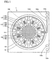
- FIG. 1 is a plan view showing a sensor chip having an MEMS structure of a condenser microphone in accordance with a first embodiment of the present invention.
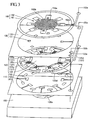
- FIG. 2 is a longitudinal sectional view showing the structure of the condenser microphone.
- FIG. 3 is an exploded view showing a lamination structure of films included in the condenser microphone.
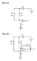
- FIG. 4A is a circuit diagram showing an equivalent circuit constituted of the sensor chip connected with a circuit chip.
- FIG. 4B is a circuit diagram showing an equivalent circuit of the sensor chip having a guard electrode connected with the circuit chip.
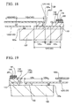
- FIG. 5 is a sectional view for use in the explanation of a first step of a manufacturing method of the condenser microphone.
- FIG. 6 is a sectional view for use in the explanation of a second step of the manufacturing method of the condenser microphone.
- FIG. 7 is a sectional view for use in the explanation of a third step of the manufacturing method of the condenser microphone.
- FIG. 8 is a sectional view for use in the explanation of a fourth step of the manufacturing method of the condenser microphone.
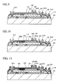
- FIG. 9 is a sectional view for use in the explanation of a fifth step of the manufacturing method of the condenser microphone.
- FIG. 10 is a sectional view for use in the explanation of a sixth step of the manufacturing method of the condenser microphone.
- FIG. 11 is a sectional view for use in the explanation of a seventh step of the manufacturing method of the condenser microphone.
- FIG. 12 is a sectional view for use in the explanation of an eighth step of the manufacturing method of the condenser microphone.
- FIG. 13 is a sectional view for use in the explanation of a ninth step of the manufacturing method of the condenser microphone.
- FIG. 14 is a sectional view for use in the explanation of a tenth step of the manufacturing method of the condenser microphone.
- FIG. 15 is a sectional view for use in the explanation of an eleventh step of the manufacturing method of the condenser microphone.
- FIG. 16 is a sectional view for use in the explanation of a twelfth step of the manufacturing method of the condenser microphone.
- FIG. 17 is a sectional view for use in the explanation of a thirteenth step of the manufacturing method of the condenser microphone.
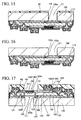
- FIG. 18 is a sectional view showing a part of the structure of the condenser microphone.
- FIG. 19 is a sectional view showing another part of the structure of the condenser microphone.
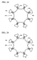
- FIG. 20 is a plan view showing a first variation of the diaphragm included in a condenser microphone in accordance with a second embodiment of the present invention.
- FIG. 21 is a plan view showing a second variation of the diaphragm included in the condenser microphone of the second embodiment of the present invention.
- FIG. 1 shows a sensor chip having an MEMS structure of a condenser microphone in accordance with a first embodiment of the present invention.
- FIG. 2 diagrammatically shows the structure of the condenser microphone.
- FIG. 3 shows the lamination structure of films included in the condenser microphone 1.
- FIG. 18 and 19 show prescribed parts of the structure of the condenser microphone 1 in detail.
- the condenser microphone 1 has a package (not shown) encapsulating the sensor chip and a circuit chip (including a power circuit and an amplification circuit, not shown).
- the sensor chip of the condenser microphone 1 is composed of multiple films deposited on a substrate 100, i.e., a lower insulating film 110, a lower conductive film 120, an upper insulating film 130, an upper conductive film 160, and a surface insulating film 170.
- a substrate 100 i.e., a lower insulating film 110, a lower conductive film 120, an upper insulating film 130, an upper conductive film 160, and a surface insulating film 170.
- the substrate 100 is composed of a P-type monocrystal silicon; but this is not a restriction.
- the material of the substrate 100 should be determined to ensure the adequate rigidity, thickness, and strength in supporting multiple thin films deposited on a base substrate.
- a through-hole having an opening 100a is formed in the substrate 100, wherein the opening 100a corresponds to the opening of a back cavity C1.
- the lower insulating film 110 joining the substrate 100, the lower conductive film 120, and the upper insulating film 130 is a deposited film composed of silicon oxide (SiOx).
- the lower insulating film 110 is used to form a plurality of third spacers 102 which are aligned in a circular manner with equal spacing therebetween, a plurality of guard spacers 103 which are aligned in a circular manner with equal spacing therebetween and are positioned internally of the third spacers 102, and a ring-shaped portion (actually, a rectangular-shaped portion having a circular opening) 101 which insulates a guard ring 125c and a guard lead 125d from the substrate 100.
- the lower conductive film 120 joining the lower insulating film 110 and the upper insulating film 130 is a deposited film composed of polycrystal silicon entirely doped with impurities such as phosphorus (P).
- the lower conductive film 120 forms the diaphragm 123 and a guard portion 127 which is constituted of guard electrodes 125a and guard connectors 125b as well as the guard ring 125c and the guard lead 125d.
- the upper insulating film 130 joining the lower conductive film 120, the upper conductive film 160, and the lower insulating film 110 is a deposited film composed of silicon oxide.
- the upper insulating film 130 forms a plurality of first spacers 131 which are aligned in a circular manner with prescribed distances therebetween, and a ring-shaped portion (actually a rectangular-shaped portion having a circular opening) 132 which is positioned outside of the first spacers 131, which supports an etching ring 161, and which insulates a plate lead 162d from the guard lead 125d.
- the upper conductive film 160 joining the upper insulating film 130 is a deposited film composed of polycrystal silicon entirely doped with impurities such as phosphorus (P).
- the upper conductive film 160 forms the plate 162, the plate lead 162d, and the etching stopper 161.
- the surface insulating film 170 joining the upper conductive film 160 and the upper insulating film 130 is a deposited film composed of silicon oxide having an insulating property.
- the MEMS structure of the condenser microphone 1 has four terminals 125e, 162e, 123e, and 100b, which are formed using a pad conductive film 180 (which is a deposited film composed of AlSi having a conductive property), a bump film 210 (which is a deposited film composed of Ni having a conductive property), and a bump protection film 220 (which is a deposited film composed of Au having a superior anti-corrosion property and a conductive property).
- a pad conductive film 180 which is a deposited film composed of AlSi having a conductive property
- a bump film 210 which is a deposited film composed of Ni having a conductive property
- a bump protection film 220 which is a deposited film composed of Au having a superior anti-corrosion property and a conductive property.
- the side walls of the terminals 125e, 162e, 123e, and 100b are protected by means of a pad protection film 190 (which is a deposited film composed of SiN having an insulating property) and a surface protection film 200 (which is a deposited film composed of silicon oxide having an insulating property).
- a pad protection film 190 which is a deposited film composed of SiN having an insulating property
- a surface protection film 200 which is a deposited film composed of silicon oxide having an insulating property
- the diaphragm 123 is formed using a thin single-layered deposited film having a conductive property and is constituted of a center portion 123a and a plurality of arms 123c which are extended outwardly in a radial direction from the center portion 123a.
- the diaphragm 123 is positioned in parallel with the substrate 100 and is supported by prescribed distances with the substrate 100 and the plate 162 while being insulated from the plate 162 by means of the third spacers 102 having pillar shapes which join the peripheral portion of the diaphragm 123 at multiple points.
- the third spacers 102 join the arms 123c of the diaphragm 123 in proximity to their distal ends.
- the diaphragm 123 Due to the cutouts formed between the arms 123c adjoining together in the diaphragm 123, the diaphragm 123 is reduced in rigidity compared with the foregoing diaphragm having no cutout.
- a plurality of diaphragm holes 123b is formed in each of the arms 123c, which is thus reduced in rigidity.
- Each arm 123c is gradually increased in breadth in a direction towards the center portion 123a of the diaphragm 123. This reduces concentration of stress at the boundary between the center portion 123a and each arm 123c.
- the diaphragm 123 is designed such that no bent portion is formed in the outline of each arm 123c in proximity to the boundary with the center portion 123a, thus preventing stress from being concentrated at the bent portion.
- the third spacers 102 are aligned in the circumferential direction with equal spacing therebetween in the surrounding area of the opening 100a of the back cavity C1.
- Each of the third spacers 102 is formed using a deposited film having an insulating property in a pillar shape.
- the diaphragm 123 is supported above the substrate 100 by the third spacers 102 such that the center portion 123a thereof covers the opening 100a of the back cavity C1 in plan view.
- a gap C2 whose height substantially corresponds to the height or thickness of the third spacer 102 is formed between the substrate 100 and the diaphragm 123. The gap C2 is required to establish a balance between the internal pressure of the back cavity C1 and the atmospheric pressure.
- the gap C2 is reduced in height and is elongated in length in the radial direction of the diaphragm 123 so as to form a maximum acoustic resistance in a path which propagate sound waves (for vibrating the diaphragm 123) to reach the opening 100a of the back cavity C1.
- a plurality of diaphragm bumps 123f is formed in the backside of the diaphragm 123 which is positioned opposite to the substrate 100.
- the diaphragm bumps 123f are projections for preventing the diaphragm 123 from being attached (or stuck) to the substrate 100. They are formed using the waviness of the lower conductive film 120 forming the diaphragm 123. Thus, dimples (or small recesses) are formed on the distal ends of the diaphragm bumps 123f.
- the diaphragm 123 is connected to the diaphragm terminal 123e via a diaphragm lead 123d which is extended from the distal end of one of the arms 123c.
- the diaphragm lead 123d is formed using the lower conductive film 120 as similarly to the diaphragm 123 in such a way that the width thereof becomes smaller than the width of the arm 123c.
- the diaphragm lead 123d is elongated to pass through the gap of the guard ring 125c toward the diaphragm terminal 123e. Since the diaphragm terminal 123e is short-circuited to the substrate terminal 100b via a circuit chip (not shown) as shown in FIGS. 4A and 4B , the same potential is applied to both of the substrate 100 and the diaphragm 123.
- a parasitic capacitance occurs between the substrate and the diaphragm 123 when the potential of the substrate 100 differs from the potential of the diaphragm 123.
- the diaphragm 123 is supported by the third spacers 102 which adjoin each other with an air gap therebetween; hence, it is possible to reduce the parasitic capacitance in the condenser microphone 1 compared with the foregoing condenser microphone whose diaphragm is supported by a spacer having a ring-shaped wall structure.
- the plate 162 is formed using a thin single-layer deposited film having a conductive property and is constituted of a center portion 162b and a plurality of arms 162a which are extended outwardly in a radial direction from the center portion 162b.
- the plate 162 is supported by the first spacers 131 having pillar shapes which join the peripheral portion of the plate 162 at multiple points.
- the plate 162 is positioned in parallel with the diaphragm 123 such that the center of the plate 162 substantially matches the center of the diaphragm 123 in plan view.
- the distance between the center of the plate 162 (i.e., the center of the center portion 162b) and the external end of the center portion 162b, i.e., the shortest distance between the center and the periphery of the plate 162, is shorter than the distance between the center of the diaphragm 123 (i.e., the center of the center portion 123a) and the external end of the center portion 123a, i.e, the shortest distance between the center and the periphery of the diaphragm 123. That is, the plate 162 is not positioned opposite to the peripheral portion of the diaphragm 123 causing a small amplitude of vibration.
- Cutouts are formed between the arms 162a of the plate 162 adjoining each other; hence, the plate 162 is not positioned opposite to the peripheral portion of the diaphragm 123 at the cutout regions thereof.
- the arms 123c of the diaphragm 123 are extended in the cutout regions of the plate 162. This increases the effective length of the diaphragm 123 causing vibration without increasing the parasitic capacitance.
- a plurality of plate holes 162c is formed in the plate 162.
- the plate holes 162c serve as passages for propagating sound waves towards the diaphragm 123, and they also serve as through-holes for transmitting an etchant used for isotropic etching performed on the upper insulating film 130.
- the remaining parts of the upper insulating film 130 after etching are used to form the first spacers 131 and the ring-shaped portion 132, while the other parts removed by etching are used to form a gap C3 between the diaphragm 123 and the plate 162. That is, the plate holes 162c serve as through-holes allowing the etchant to reach the upper insulating film 130 so as to simultaneously form the first spacers 131 and the gap C3.
- the plate holes 162c are appropriately aligned in consideration of the height of the gap C3, the shapes of the first spacers 130, and the etching speed. Specifically, the plate holes 162c are collectively formed with equal spacing therebetween in the center portion 162b and the arms 162a except for the joint portions of the plate 162 joining with the first spacers 131. As the distances between the adjacent plate holes 162c get smaller, it is possible to reduce the width of the ring-shaped portion 132 (formed using the upper insulating film 130), thus reducing the overall size of a chip. On the other hand, the rigidity of the plate 162 gets smaller as the distances between the adjacent plate holes 162c get smaller.
- the first spacers 131 join the guard electrodes 125a, which are positioned at the same position as the diaphragm 123 and which are formed using the lower conductive film 120 forming the diaphragm 123.
- the first spacers 131 are formed using the upper insulating film 130, i.e., a deposited film having an insulating property joined to the plate 162.
- the first spacers 131 are aligned with equal spacing therebetween in the surrounding area of the opening 100a of the back cavity C1.
- the first spacers 131 are positioned in the cutout regions between the arms 123c adjoining each other in the diaphragm 123, it is possible to reduce the maximum diameter of the plate 162 to be smaller than the maximum diameter of the diaphragm 123. This relatively increases the rigidity of the plate 162 while reducing the parasitic capacitance between the plate 162 and the substrate 100.
- the plate 162 is supported above the substrate 100 by means of a plurality of second spacers 129 having pillar shapes which are constituted of the guard spacers 103, the guard electrodes 125a, and the first spacers 131.
- the second spacers 129 are each formed in a multilayered structure including deposited films.
- the gap C3 is formed between the plate 162 and the diaphragm 123 by the second spacers 129, so that the gaps C2 and C3 are formed between the plate 162 and the substrate 100. Due to insulating properties of the guard spacers 103 and the first spacers 131, the plate 162 is insulated from the substrate 100.
- the second spacers 129 having pillar shapes are formed using the guard spacers 103, the guard electrodes 125a, and the first spacers 131, wherein they are physically isolated from each other so as to support the plate 162 above the substrate 100.
- a plurality of plate bumps 162f is formed on the backside of the plate 162 positioned opposite to the diaphragm 123.
- the plate bumps 162f are formed using a silicon nitride film (SiN) joining the upper conductive film 160, and a polycrystal silicon film joining the silicon nitride film.
- SiN silicon nitride film
- the plate bumps 162f prevent the diaphragm 123 from being attached (or stuck) to the plate 162.
- a plate lead 162d whose width is smaller than the width of the arm 162a is extended from the distal end of the arm 162a of the plate 162 toward the plate terminal 162e.
- the plate lead 162d is formed using the upper conductive film 160 forming the plate 162.
- the wiring path of the plate lead 162d substantially overlap the wiring path of the guard lead 125d in plan view; hence, it is possible to reduce the parasitic capacitance formed between the plate lead 162d and the substrate 100.
- FIGS. 4A and 4B each of which shows an equivalent circuit including the sensor chip and the circuit chip which are connected together.
- a charge pump P included in the circuit chip applies a stable bias voltage to the diaphragm 123.
- the sensitivity of the condenser microphone 1 increases as the bias voltage increases, wherein adherence (or stiction) may easily occur between the diaphragm 123 and the plate 162. For this reason, the rigidity of the plate is an important factor in designing the MEMS structure of the condenser microphone 1.
- Sound waves (entered from a through-hole of a package, not shown) are transmitted through the plate holes 162c and the cutout regions between the arms 162a of the plate 162 so as to reach the diaphragm 123. Since sound waves of the same phase are propagated along both of the surface and backside of the plate 162, the plate 162 would not vibrate substantially. Sound waves reaching the diaphragm 123 make the diaphragm 123 vibrate relative to the plate 162.
- the electrostatic capacitance of a parallel-plate condenser constituted of opposite electrodes (corresponding to the diaphragm 123 and the plate 162) is varied. Variations of electrostatic capacitance are converted into electric signals, which are then amplified by an amplifier A included in the circuit chip.
- the amplifier A should be necessarily installed in the package because of the high-impedance output of the sensor chip.
- the diaphragm 123 Since the diaphragm 123 is short-circuited with the substrate 100, a parasitic capacitance is formed between the substrate 100 and the plate 162 (which does not vibrate relatively) in the circuitry of FIG. 4A which does not include the guard electrode 125a in the guard portion 127.
- the output terminal of the amplifier A is connected to the guard portion 127 so as to form a voltage-follower circuit using the amplifier A, whereby it is possible to avoid the occurrence of the parasitic capacitance between the plate 162 and the substrate 100.
- the guard electrodes 125a are arranged between the substrate 100 and the arms 162a of the plate 162 in the prescribed regions in which the arms 162a are positioned opposite to the substrate 100 in plan view, it is possible to reduce the parasitic capacitance between the substrate 100 and the arms 162a of the plate 162. Due to the wiring of the guard lead 125d (which is extended from the guard ring 125c connecting the guard electrodes 125a together toward the guard terminal 125e) in the region in which the plate lead 162d (which is extended from the arm 162a of the plate 162) is positioned opposite to the substrate 100 in plan view, no parasitic capacitance is formed between the plate lead 162d and the substrate 100.
- the guard ring 125c connects the guard electrodes 125a together substantially with the minimum distances therebetween in the surrounding area of the diaphragm 123.
- the constituent elements of the circuit chip such as the charge pump P and the amplifier A into the sensor chip, thus forming the condenser microphone 1 having a single-chip structure.
- the lower insulating film 110 composed of silicon oxide is entirely formed on the surface of the substrate 100.
- a lower insulating film 110 is etched using a photoresist mask so as to form dimples 110a used for the formation of the diaphragm bumps 123f.
- the lower conductive film 120 composed of polycrystal silicon is formed on the surface of the lower insulating film 110 by way of CVD (i.e. Chemical Vapor Deposition).
- CVD i.e. Chemical Vapor Deposition
- the diaphragm bumps 123f are formed on the dimples 110a.
- the lower conductive film 120 is etched using a photoresist mask so as to form the diaphragm 123 and the guard portion 127, both of which are formed using the lower conductive film 120.
- the upper insulating film 130 composed of silicon oxide is entirely formed on the surfaces of the lower insulating film 110 and the lower conductive film 120.
- etching is performed using a photoresist mask so as to form dimples 130a (used for the formation of the plate bumps 162f) in the upper insulating film 130.
- the plate bumps 162f are formed using a polysilicon film 135 and a silicon nitride film 136 on the surface of the upper insulating film 130. Since the silicon nitride film 136 is formed after the patterning of the polycrystal silicon film 135 by way of the known method, all the exposed portions of the polysilicon film 135 which project from the dimples 130a are covered with the silicon nitride film 136.
- the silicon nitride film 136 is an insulating film that prevents the diaphragm 123 from being short-circuited with the plate 162 in adherence (or stiction).
- the upper conductive film 160 composed of polycrystal silicon is formed on the exposed surface of the upper insulating film 130 and the surface of the silicon nitride film 136 by way of CVD.
- the upper conductive film 160 is etched using a photoresist mask so as to form the plate 162, the plate lead 162d, and the etching stopper 161. In this step, the plate holes 162c are not formed in the plate 162.
- contact holes CH1, CH3, and CH4 are formed in the upper insulating film 130; subsequently, the surface insulating film 170 composed of silicon oxide is formed on the entire surface.
- the surface insulating film 170 is etched using a photoresist mask so as to form a contact hole CH2 and to simultaneously remove the prescribed portions of the surface insulating film 170 remaining in the bottoms of the contact holes CH1, CH3, and CH4.
- a pad conductive film 180 composed of AlSi is formed and embedded in the contact holes CH1, CH2, CH3, and CH4.
- the pad conductive film 180 is subjected to patterning so as to leave the prescribed portions covering the contact holes CH1, CH2, CH3, and CH4 in accordance with the known method. Furthermore, a pad protection film 190 composed of silicon nitride is formed on the surface insulating film 170 and the pad conductive film 180 by way of CVD. Then, the pad conductive film 190 is subjected to patterning by way of the known method, thus leaving prescribed portions thereof in the surrounding area of the pad conductive film 180.
- anisotropic etching is performed using a photoresist mask so as to form holes 170a in correspondence with the plate holes 162c, whereby the plate holes 162c are formed in the upper conductive film 160.
- This step is performed continuously so that the surface insulating film 170 having the holes 170a serves as a resist mask for the upper conductive film 160.
- a surface protection film 200 composed of silicon oxide is formed on the surfaces of the surface insulating film 170 and the pad protection film 190.
- the surface protection film 200 is partially embedded in the holes 170a of the surface insulating film 170 and the plate holes 162c.
- a bump film 210 composed of Ni is formed on the prescribed portions of the pad conductive film 180 embedded in the contact holes CH1, CH2, CH3, and CH4. Then, a bump protection film 220 composed of Au is formed on the surface of the bump film 210. In this step, the backside of the substrate 100 is polished so as to define the desired thickness for the substrate 100.
- etching is performed using a photoresist mask on the surface protection film 200 and the surface insulating film 170 so as to form a through-hole H5 for exposing the etching stopper 161.
- the film formation process is completed with respect to the surface side of the substrate 100 by way of the aforementioned steps.
- a photoresist mask R1 having a through-hole H6 (used for the formation of the back cavity C1) is formed on the backside of the substrate 100 in a tenth step of the manufacturing method shown in FIG. 14 .
- Deep-RIE where RIE stands for Reactive Ion Etching
- RIE Reactive Ion Etching
- the photoresist mask R1 is removed, then a wall surface 100c of the through-hole (which is roughly formed in the substrate 100 by way of Deep-RIE) is smoothed.
- isotropic etching is performed using a photoresist mask R2 and a buffered hydrofluoric acid (BHF) the surface protection film 200 and the surface insulating film 170 are removed from the plate 162 and the plate lead 162d.
- BHF buffered hydrofluoric acid
- the ring-shaped portion 132, the first spacers 131, and the gap C3 are formed by partially removing the upper insulating film 130.
- the guard spacer 103, the third spacers 102, the ring-shaped portion 101, and the gap C2 are formed by partially removing the lower insulating film 110.
- the BHF serving as an etchant enters into a through-hole H6 of the photoresist mask R2 and the opening 100a of the substrate 100.
- the outline of the upper insulating film 130 is defined by the plate 162 and the plate lead 162d. That is, the ring-shaped portion 132 and the first spacers 131 are formed by way of self-alignment of the plate 162 and the plate lead 162d. As shown in FIG. 18 , undercuts are formed on the edges of the ring-shaped portion 132 and the first spacers 131 by way of isotropic etching.
- the outline of the lower insulating film 110 is defined by the opening 100a of the substrate 100, the diaphragm 123, the diaphragm lead 123d, the guard electrodes 125a, the guard connectors 125b, and the guard ring 125c. That is, the guard spacer 103 and the third spacers 102 are formed by way of self-alignment of the diaphragm 123. In addition, undercuts are formed on the edges of the guard spacers 103 and the first spacers 131 by way of isotropic etching (see FIGS. 18 and 19 ). Since the guard spacers 103 and the first spacers 131 are formed in this step, the second spacers 129 for supporting the plate 162 above the substrate 100 are formed except for the guard electrodes 125a.
- the photoresist mask R2 is removed, then the substrate 100 is subjected to dicing, thus completing the production of the sensor chip of the condenser microphone 1.
- the sensor chip and the circuit chip are bonded onto the substrate of the package; the aforementioned terminals are connected together by way of wire bonding; then, a package cover (not shown) is mounted on the substrate of the package; thus, it is possible to close the back cavity C1 in an airtight manner in the backside of the substrate 100.
- the second embodiment of the present invention is directed to the condenser microphone 1, which is described with reference to FIGS. 1 to 19 , wherein the third spacers 102 are referred to as diaphragm supports 102, the second spacers 129 are referred to as plate supports 129, and the first spacers 131 are referred to as plate spacers.
- the sensitivity can be increased by increasing the rigidity of the plate 162
- the rigidity of the diaphragm 123 may have a difficulty in achieving an adequate durability.
- the second embodiment is designed to increase the sensitivity and durability of the condenser microphone 1 in which the diaphragm 123 is supported using pillar structures without substantially increasing the size of the condenser microphone 1.
- the condenser microphone 1 according to the second embodiment has a constitution substantially identical to that of the first embodiment, the detailed description thereof will not be repeated, whereas the second embodiment can be explained in more detail by way of the following descriptions.
- Each of the arms 123c of the diaphragm 123 is increased in width in each of the joint regions at which the arms 123c join the diaphragm supports 102 and is elongated in length in the circumferential direction of the diaphragm 123. Specifically, each of the arms 123c of the diaphragm 123 becomes narrow in width in proximity to the center portion 123a in the direction departing from the center portion 123a, while it becomes wider in width in proximity to and toward each of the diaphragm supports 102.
- the width of the arm 123c in the circumferential direction of the diaphragm 123 becomes shortest in the intermediate region between the center portion 123a and the diaphragm support 102 but becomes longer in the region at which the arm 123c joins the diaphragm support 102. For this reason, it is possible to increase the durability while increasing the overall joint area between the diaphragm 123 and the diaphragm supports 102 without substantially increasing the overall radius of the diaphragm 123.
- the width of the arm 123c (lying in the circumferential direction of the diaphragm 123) becomes longest in the region in which the arm 123c joins the diaphragm support 102, it is possible to secure high joint strength of the diaphragm 123 while reducing the rigidity of the diaphragm 123.
- the diaphragm supports 102 are positioned between the arms (or joint portions) 162a of the plate 162 and externally of the plate supports 129 in the radial direction of the plate 162. This reduces the rigidity of the diaphragm 123 compared with the rigidity of the plate 162.
- the widths of the diaphragm supports 102 (in the circumferential direction of the diaphragm 123) are longer than the widths of the arms 123c in their regions positioned between the center portion 123a of the diaphragm 123 and the diaphragm supports 102.
- the gap C2 whose height substantially matches the thickness of the diaphragm supports 102 is formed between the substrate 100 and the diaphragm 123. As described above, the gap is required to establish a balance between the internal pressure of the back cavity C1 and the atmospheric pressure.
- the overall operation of the condenser microphone 1 of the second embodiment is identical to that of the first embodiment which is described with reference to FIGS. 4A and 4B ; hence, the description thereof will not be repeated.
- the manufacturing method of the condenser microphone 1 of the second embodiment is identical to that of the first embodiment which is described with reference to FIGS. 5 to 17 ; hence, the description thereof will not be repeated.
- the diaphragm 123 adapted to the second embodiment is identical to that of the first embodiment shown in FIGS. 1 and 3 ; but the second embodiment provides variations of the diaphragm 123, which will be described below.
- FIGS. 20 and 21 shows variations of the diaphragm 123, in which the outlines of the arms 123c adjoining together in the diaphragm 123 smoothly join the outline of the center portion 123a and are each curved inwardly in the circumferential direction of the diaphragm 123.
- FIG. 20 shows a first variation of the diaphragm 123 in which the outline thereof is seamlessly curved between the center portion 123a and the joint regions of the arms 123c joining the diaphragm supports 102 without bent portions, wherein it is possible to reduce concentration of stress at the arms 123c of the diaphragm 123, which are thus not bent easily.
- FIG. 20 shows a first variation of the diaphragm 123 in which the outline thereof is seamlessly curved between the center portion 123a and the joint regions of the arms 123c joining the diaphragm supports 102 without bent portions, wherein it is possible to reduce concentration of stress at the arms 123c of the diaphragm 123, which
- FIGS. 20 and 21 shows a second variation of the diaphragm 123 in which the outline thereof smoothly continues between the arms 123c and the center portion 123a.
- the diaphragm holes 123b are not aligned in the circumferential direction of the diaphragm 123, whereby it is possible to reduce concentration of stress at the arms 123c, which are thus hardly bent.
- the aforementioned materials and dimensions are merely illustrative and not restrictive, wherein the descriptions regarding the addition, deletion, and change of order of steps in manufacturing, which may be obvious to those skilled in the art are omitted for the sake of simplicity of the explanation.
- the film composition, film formation method, outline formation methods of films, and order of steps in manufacturing are not necessarily limited those described above but can be appropriately selected in consideration of the combination of materials of films having desired properties, thicknesses of films, required precisions for defining outlines of films, and the like.
Abstract
A vibration transducer is constituted of a substrate, a diaphragm having a conductive property, a plate having a conductive property, and a plurality of first spacers having pillar shapes which are formed using a deposited film having an insulating property joining the plate so as to support the plate relative to the diaphragm with a gap therebetween. It is possible to introduce a plurality of second spacers having pillar shapes support the plate relative to the substrate with a gap therebetween, and/or a plurality of third spacers having pillar shapes which support the diaphragm relative to the substrate with a gap therebetween. When the diaphragm vibrates relative to the plate, an electrostatic capacitance formed therebetween is varied so as to detect vibration with a high sensitivity. The diaphragm has a plurality of arms whose outlines are curved so that the intermediate regions thereof are reduced in width.
Description
- The present invention relates to vibration transducers and in particular to wave transducers such as miniature condenser microphones serving as MEMS sensors. The present invention also relates to manufacturing methods of vibration transducers.
- The present application claims priority on Japanese Patent Application No.
2007-256905 2007-256906 - Various types of vibration transducers have been developed and disclosed in various documents such as
Patent Documents 1, 2, 3 andNon-Patent Document 1. - Patent Document 1: Japanese Patent Application Publication No.
H09-508777 - Patent Document 2: Japanese Patent Application Publication No.
2004-506394 - Patent Document 3:
U.S. Patent No. 4,776,019 - Non-Patent Document 1: The paper entitled "MSS-01-34" published by the Japanese Institute of Electrical Engineers
- Miniature condenser microphones have been conventionally known as typical types of vibration transducers and have been produced by way of semiconductor device manufacturing processes.
- Condenser microphones are referred to as MEMS microphones (where MEMS stands for Micro Electro Mechanical System). A typical example of condenser microphones is constituted of a substrate, a diaphragm, and a plate. The diaphragm and plate serving as opposite electrodes, which are distanced from each other, are composed of films deposed on the substrate and are supported above the substrate. When the diaphragm vibrates due to sound waves relative to the plate, the electrostatic capacitance between the diaphragm and the plate varies due to the displacement of the diaphragm, and then variations of electrostatic capacitance are converted into electric signals. This condenser microphone (or vibration transducer) is designed such that the peripheral portion of the plate joins an insulating film.
- In the structure in which the plate joins the insulating film, however, a parasitic capacitance occurs between the diaphragm or the substrate and the plate which joins the insulating film serving as a dielectric layer in the peripheral portion, thus reducing the sensitivity of the vibration transducer.
- It is an object of the present invention to provide a vibration transducer having high sensitivity.
- It is another object of the present invention to provide a manufacturing method of the vibration transducer.
- In a first aspect of the present invention, a vibration transducer includes a diaphragm having a conductive property, a plate having a conductive property, which is positioned opposite to the diaphragm, and a plurality of first spacers having pillar shapes which are formed using a deposited film having an insulating property joining the plate and which supports the plate relative to the diaphragm with a gap therebetween, wherein an electrostatic capacitance formed between the diaphragm and the plate is varied when the diaphragm vibrates relative to the plate.
- In the fixed region of the diaphragm which does not vibrate relative to the plate, a parasitic capacitance is formed between the diaphragm and the plate, which are positioned opposite to each other; hence, it is preferable that the first spacers each having a high dielectric constant (higher than that of the air) be each reduced in area in plan view. That is, the plate is supported by the first spacers, which are not formed in ring shapes but are formed in a pillar shape, whereby it is possible to reduce the electrostatic capacitance between the diaphragm and the plate, thus improving the sensitivity. The geometric shapes of the first spacers are not necessarily limited to pillar shapes but can also be formed in flat shapes. The present invention does not need the support having a structurally closed shape but multiple supports which are formed in any shape for supporting the plate. It may be possible to reduce the parasitic capacitance by forming the plate or the diaphragm by use of an insulating substance in the region in which the diaphragm and the plate is positioned opposite to each other; however, this causes complexity in film structure with respect to at least one of the diaphragm and the plate
- The aforementioned vibration transducer is manufactured in such a way that a plurality of holes are formed in the plate; isotropic etching is performed using the plate as a mask so as to remove a part of the deposited film, thus forming the gap between the plate and the diaphragm; and the first spacers are formed by use of the remaining deposited film. Since the plate is used as the etching mask so as to form the first spacers, it is possible to reduce the total number of masks, thus reducing the manufacturing cost.
- That is, it is preferable that the plate has a plurality of holes which allow an etchant to transmit therethrough in isotropic etching, thus simultaneously forming the first spacers and the gap between the plate and the diaphragm.
- The vibration transducer further includes a substrate and a plurality of second spacers having pillar shapes which are formed using a deposited film having an insulating property and which support the plate relative to the substrate with a gap therebetween, wherein an electrostatic capacitance formed between the diaphragm and the plate is varied when the diaphragm vibrates relative to the plate.
- In consideration of a parasitic capacitance formed in the region in which the plate and the substrate are positioned opposite to each other via the second spacers having high dielectric constants (higher than the dielectric constant of the air) therebetween, it is preferable that the second spacers each be reduced in area in plan view. That is, the plate is supported by the second spacers which are formed not in ring shapes but in pillar shapes, whereby it is possible to reduce the electrostatic capacitance between the substrate and the plate, thus improving the sensitivity of the vibration transducer. The geometric shapes of the second spacers are not necessarily limited to pillar shapes but can also be formed in flat shapes. The present invention does not need the support having a structurally closed shape but multiple supports which are formed in any shapes for supporting the plate. It may be possible to reduce the parasitic capacitance in the region in which the plate and the substrate are positioned opposite to each other with the second spacers therebetween by forming the prescribed region of the plate joining the second spacers by use of an insulating substance; however, this causes complexity in the film structure of the plate.
- The vibration transducer is manufactured in such a way that a plurality of holes is formed in the plate; isotropic etching is performed using the plate as a mask so as to remove a part of the deposited film, thus forming the gap between the plate and the substrate; and the second spacers are formed using the remaining of the deposited film. Since the plate is used as an etching mask for use in the formation of the second spacers, it is possible to reduce the number of masks, thus reducing the manufacturing cost.
- That is, it is preferable that the plate has a plurality of holes allowing an etchant to transmit therethrough in isotropic etching, thus simultaneously forming the second spacers and the gap between the plate and the substrate.
- In the vibration transducer, the distance between the center and the external end of the plate is smaller than the distance between the center and the external end of the diaphragm. In the region in which the diaphragm causes a relatively small amplitude of vibration or causes substantially no vibration, the electrostatic capacitance between the diaphragm and the plate varies very little or is not varied substantially. In the foregoing structure in which the external portion of the diaphragm is fixed to its upper or lower film, it causes a very small amplitude of vibration. The vibration transducer is designed such that the distance between the center and the external end of the plate becomes smaller than the distance between the center and the external end of the diaphragm, thus inhibiting the external portion of the diaphragm from being positioned opposite to the plate. When the plate and the diaphragm are both formed in a circular shape or when they have no recess in the outlines thereof, it is required that the external end of the plate is positioned inwardly of the external end of the diaphragm. When the plate and the diaphragm are both formed in a circular shape or when they have no recess in the outlines thereof, it is required that the shortest distance between the center and the external end of the plate be shorter than the shortest distance between the center and the external end of the diaphragm. Even when the plate is formed in a circular shape or does not have a recess in the outline thereof and even when the diaphragm has recesses in the outline thereof, it is required that the shortest distance between the center and the external end of the plate be shorter than the shortest distance between the center and the external end of the diaphragm. The aforementioned structure of the vibration transducer is capable of reducing the parasitic capacitance between the diaphragm and the plate, thus improving the sensitivity. In this connection, it may be possible to reduce the parasitic capacitance by forming the external portion of the diaphragm by use of an insulating substance or by forming the external region of the plate positioned opposite to the external portion of the diaphragm by use of an insulating substance, whereas this causes complexity in the film structure of at least one of the plate and the diaphragm.
- Alternatively, the vibration transducer further includes a plurality of third spacers having pillar shapes which are formed using a deposited film having an insulating property which joins the substrate and the diaphragm and which supports the diaphragm relative to the substrate with a gap therebetween. When a parasitic capacitance is formed between the diaphragm and the substrate in the region in which they are positioned opposite to each other via the third spacers, it is preferable that the area of the third spacer (whose dielectric constant is higher than that of the air) be as small as possible. Each of the third spacers is not formed in a ring shape but in a pillar shape, whereby the diaphragm is supported by multiple third spacers; thus, it is possible to reduce the parasitic capacitance between the substrate and the diaphragm, thus improving the sensitivity. The geometric shapes of the third spacers are not necessarily limited to pillar shapes but can be formed in flat shapes. It is required that the third spacer not be formed in a closed wall structure, but a plurality of third spacers be formed in any shape for supporting the diaphragm. In this connection, it may be possible to reduce the parasitic capacitance between the diaphragm and the substrate in the region in which they are positioned opposite to each other via the third spacers by forming joint portions of the diaphragm joining the third spacers by use of insulating materials; however, this causes complexity in the film structure of the diaphragm.
- Moreover, the plate is constituted of a center portion and a plurality of arms which are extended outwardly in a radial direction from the center portion, whereby the diaphragm is not positioned opposite to the plate at the arms and in the cutout regions between the arms. Due to the formation of the arms which are extended outwardly in a radial direction from the center portion of the plate, it is possible to reduce the parasitic capacitance formed between the diaphragm and the plate.
- In a second aspect of the present invention, a vibration transducer includes a substrate, a diaphragm having a conductive property which is constituted of a center portion and a plurality of arms extended outwardly in a radial direction from the center portion, a plate having a conductive property which is constituted of a center portion, which is positioned opposite to the center portion of the diaphragm, and a plurality of arms extended outwardly in a radial direction from the center portion thereof, a plurality of plate supports for supporting the plate, and a plurality of diaphragm supports having pillar shapes which are positioned between the cutouts formed between the arms of the plate and which are positioned outwardly of the plate supports in the radial direction of the plate so as to support the diaphragm. The width of each arm of the diaphragm in the circumferential direction of the diaphragm becomes shortest in the intermediate region between the center portion and the joint portion at which each arm joins each diaphragm support but becomes longer in proximity to the joint portion. Herein, an electrostatic capacitance formed between the diaphragm and the plate is varied when the diaphragm vibrates relative to the plate.
- In the above, the arms of the diaphragm are positioned alternately with the arms of the plate in plan view, wherein the distance between the plate supports which are positioned opposite to each other so as to support the plate is shorter than the distance between the diaphragm supports which are positioned opposite to each other so as to support the diaphragm. That is, the diaphragm supports which join the arms of the diaphragm and the substrate are positioned between the plate supports in the circumferential direction of the plate and are positioned externally of the plate supports in the radial direction of the plate. This increases the rigidity of the plate to be relatively higher than the rigidity of the diaphragm. The joint strength between the arms of the diaphragm and the diaphragm supports increase as the joint areas therebetween increase; thus, it is possible to increase the durability of the vibration transducer. When the joint areas are increased by increasing the lengths of the diaphragm supports in the radial direction of the diaphragm, the rigidity of the diaphragm is not changed (so that the sensitivity is not increased) irrespective of the substantial length of the diaphragm between the diaphragm supports, whereas the vibration transducer may be increased in size. To cope with such a possible drawback, the widths of the arms of the diaphragm in its circumferential direction are broadened at the joint areas so as to broaden the joint areas between the arms of the diaphragm and the diaphragm supports. This makes it possible to increase the sensitivity and durability of the vibration transducer without increasing its size. The geometric shapes of the diaphragm supports are not necessarily limited to pillar shapes but can be formed in flat shapes. That is, it is required for the diaphragm support to not have a structurally closed-wall structure but should be formed in any shape for supporting the diaphragm.
- The rigidity of the diaphragm decreases as the widths of the arms of the diaphragm become short; hence, it is preferable that the widths of the arms of the diaphragm should be mostly broadened at the joint regions joining the diaphragm supports. That is, it is preferable that the widths of the arms of the diaphragm become longest at the joint regions joining the diaphragm supports.
- It is preferable that the widths of the diaphragm supports be longer than the shortest width of the arm of the diaphragm at the intermediate position between the diaphragm support and the center portion of the diaphragm.
- These and other objects, aspects, and embodiments of the present invention will be described in more detail with reference to the following drawings.
-
FIG. 1 is a plan view showing a sensor chip having an MEMS structure of a condenser microphone in accordance with a first embodiment of the present invention. -
FIG. 2 is a longitudinal sectional view showing the structure of the condenser microphone. -
FIG. 3 is an exploded view showing a lamination structure of films included in the condenser microphone. -
FIG. 4A is a circuit diagram showing an equivalent circuit constituted of the sensor chip connected with a circuit chip. -
FIG. 4B is a circuit diagram showing an equivalent circuit of the sensor chip having a guard electrode connected with the circuit chip. -
FIG. 5 is a sectional view for use in the explanation of a first step of a manufacturing method of the condenser microphone. -
FIG. 6 is a sectional view for use in the explanation of a second step of the manufacturing method of the condenser microphone. -
FIG. 7 is a sectional view for use in the explanation of a third step of the manufacturing method of the condenser microphone. -
FIG. 8 is a sectional view for use in the explanation of a fourth step of the manufacturing method of the condenser microphone. -
FIG. 9 is a sectional view for use in the explanation of a fifth step of the manufacturing method of the condenser microphone. -
FIG. 10 is a sectional view for use in the explanation of a sixth step of the manufacturing method of the condenser microphone. -
FIG. 11 is a sectional view for use in the explanation of a seventh step of the manufacturing method of the condenser microphone. -
FIG. 12 is a sectional view for use in the explanation of an eighth step of the manufacturing method of the condenser microphone. -
FIG. 13 is a sectional view for use in the explanation of a ninth step of the manufacturing method of the condenser microphone. -
FIG. 14 is a sectional view for use in the explanation of a tenth step of the manufacturing method of the condenser microphone. -
FIG. 15 is a sectional view for use in the explanation of an eleventh step of the manufacturing method of the condenser microphone. -
FIG. 16 is a sectional view for use in the explanation of a twelfth step of the manufacturing method of the condenser microphone. -
FIG. 17 is a sectional view for use in the explanation of a thirteenth step of the manufacturing method of the condenser microphone. -
FIG. 18 is a sectional view showing a part of the structure of the condenser microphone. -
FIG. 19 is a sectional view showing another part of the structure of the condenser microphone. -
FIG. 20 is a plan view showing a first variation of the diaphragm included in a condenser microphone in accordance with a second embodiment of the present invention. -
FIG. 21 is a plan view showing a second variation of the diaphragm included in the condenser microphone of the second embodiment of the present invention. - The present invention will be described in further detail by way of examples with reference to the accompanying drawings.
-
FIG. 1 shows a sensor chip having an MEMS structure of a condenser microphone in accordance with a first embodiment of the present invention.FIG. 2 diagrammatically shows the structure of the condenser microphone.FIG. 3 shows the lamination structure of films included in thecondenser microphone 1.FIG. 18 and 19 show prescribed parts of the structure of thecondenser microphone 1 in detail. Thecondenser microphone 1 has a package (not shown) encapsulating the sensor chip and a circuit chip (including a power circuit and an amplification circuit, not shown). - The sensor chip of the
condenser microphone 1 is composed of multiple films deposited on asubstrate 100, i.e., a lower insulatingfilm 110, a lowerconductive film 120, an upperinsulating film 130, an upperconductive film 160, and asurface insulating film 170. The lamination of films included in the MEMS structure of thecondenser microphone 1 will be described below. - The
substrate 100 is composed of a P-type monocrystal silicon; but this is not a restriction. The material of thesubstrate 100 should be determined to ensure the adequate rigidity, thickness, and strength in supporting multiple thin films deposited on a base substrate. A through-hole having anopening 100a is formed in thesubstrate 100, wherein theopening 100a corresponds to the opening of a back cavity C1. - The lower
insulating film 110 joining thesubstrate 100, the lowerconductive film 120, and the upper insulatingfilm 130 is a deposited film composed of silicon oxide (SiOx). The lowerinsulating film 110 is used to form a plurality ofthird spacers 102 which are aligned in a circular manner with equal spacing therebetween, a plurality ofguard spacers 103 which are aligned in a circular manner with equal spacing therebetween and are positioned internally of thethird spacers 102, and a ring-shaped portion (actually, a rectangular-shaped portion having a circular opening) 101 which insulates aguard ring 125c and aguard lead 125d from thesubstrate 100. - The lower
conductive film 120 joining the lower insulatingfilm 110 and the upper insulatingfilm 130 is a deposited film composed of polycrystal silicon entirely doped with impurities such as phosphorus (P). The lowerconductive film 120 forms thediaphragm 123 and aguard portion 127 which is constituted ofguard electrodes 125a andguard connectors 125b as well as theguard ring 125c and theguard lead 125d. - The upper
insulating film 130 joining the lowerconductive film 120, the upperconductive film 160, and the lower insulatingfilm 110 is a deposited film composed of silicon oxide. The upperinsulating film 130 forms a plurality offirst spacers 131 which are aligned in a circular manner with prescribed distances therebetween, and a ring-shaped portion (actually a rectangular-shaped portion having a circular opening) 132 which is positioned outside of thefirst spacers 131, which supports anetching ring 161, and which insulates aplate lead 162d from theguard lead 125d. - The upper
conductive film 160 joining the upper insulatingfilm 130 is a deposited film composed of polycrystal silicon entirely doped with impurities such as phosphorus (P). The upperconductive film 160 forms theplate 162, theplate lead 162d, and theetching stopper 161. - The
surface insulating film 170 joining the upperconductive film 160 and the upper insulatingfilm 130 is a deposited film composed of silicon oxide having an insulating property. - The MEMS structure of the
condenser microphone 1 has fourterminals terminals - Next, the mechanical structure of the MEMS structure of the
condenser microphone 1 will be described below. - The
diaphragm 123 is formed using a thin single-layered deposited film having a conductive property and is constituted of acenter portion 123a and a plurality ofarms 123c which are extended outwardly in a radial direction from thecenter portion 123a. Thediaphragm 123 is positioned in parallel with thesubstrate 100 and is supported by prescribed distances with thesubstrate 100 and theplate 162 while being insulated from theplate 162 by means of thethird spacers 102 having pillar shapes which join the peripheral portion of thediaphragm 123 at multiple points. Specifically, thethird spacers 102 join thearms 123c of thediaphragm 123 in proximity to their distal ends. Due to the cutouts formed between thearms 123c adjoining together in thediaphragm 123, thediaphragm 123 is reduced in rigidity compared with the foregoing diaphragm having no cutout. A plurality ofdiaphragm holes 123b is formed in each of thearms 123c, which is thus reduced in rigidity. Eacharm 123c is gradually increased in breadth in a direction towards thecenter portion 123a of thediaphragm 123. This reduces concentration of stress at the boundary between thecenter portion 123a and eacharm 123c. Thediaphragm 123 is designed such that no bent portion is formed in the outline of eacharm 123c in proximity to the boundary with thecenter portion 123a, thus preventing stress from being concentrated at the bent portion. - The
third spacers 102 are aligned in the circumferential direction with equal spacing therebetween in the surrounding area of theopening 100a of the back cavity C1. Each of thethird spacers 102 is formed using a deposited film having an insulating property in a pillar shape. Thediaphragm 123 is supported above thesubstrate 100 by thethird spacers 102 such that thecenter portion 123a thereof covers theopening 100a of the back cavity C1 in plan view. A gap C2 whose height substantially corresponds to the height or thickness of thethird spacer 102 is formed between thesubstrate 100 and thediaphragm 123. The gap C2 is required to establish a balance between the internal pressure of the back cavity C1 and the atmospheric pressure. The gap C2 is reduced in height and is elongated in length in the radial direction of thediaphragm 123 so as to form a maximum acoustic resistance in a path which propagate sound waves (for vibrating the diaphragm 123) to reach theopening 100a of the back cavity C1. - A plurality of
diaphragm bumps 123f is formed in the backside of thediaphragm 123 which is positioned opposite to thesubstrate 100. The diaphragm bumps 123f are projections for preventing thediaphragm 123 from being attached (or stuck) to thesubstrate 100. They are formed using the waviness of the lowerconductive film 120 forming thediaphragm 123. Thus, dimples (or small recesses) are formed on the distal ends of the diaphragm bumps 123f. - The
diaphragm 123 is connected to thediaphragm terminal 123e via adiaphragm lead 123d which is extended from the distal end of one of thearms 123c. Thediaphragm lead 123d is formed using the lowerconductive film 120 as similarly to thediaphragm 123 in such a way that the width thereof becomes smaller than the width of thearm 123c. Thediaphragm lead 123d is elongated to pass through the gap of theguard ring 125c toward thediaphragm terminal 123e. Since thediaphragm terminal 123e is short-circuited to thesubstrate terminal 100b via a circuit chip (not shown) as shown inFIGS. 4A and 4B , the same potential is applied to both of thesubstrate 100 and thediaphragm 123. - A parasitic capacitance occurs between the substrate and the
diaphragm 123 when the potential of thesubstrate 100 differs from the potential of thediaphragm 123. Herein, thediaphragm 123 is supported by thethird spacers 102 which adjoin each other with an air gap therebetween; hence, it is possible to reduce the parasitic capacitance in thecondenser microphone 1 compared with the foregoing condenser microphone whose diaphragm is supported by a spacer having a ring-shaped wall structure. - The
plate 162 is formed using a thin single-layer deposited film having a conductive property and is constituted of acenter portion 162b and a plurality ofarms 162a which are extended outwardly in a radial direction from thecenter portion 162b. Theplate 162 is supported by thefirst spacers 131 having pillar shapes which join the peripheral portion of theplate 162 at multiple points. Theplate 162 is positioned in parallel with thediaphragm 123 such that the center of theplate 162 substantially matches the center of thediaphragm 123 in plan view. Herein, the distance between the center of the plate 162 (i.e., the center of thecenter portion 162b) and the external end of thecenter portion 162b, i.e., the shortest distance between the center and the periphery of theplate 162, is shorter than the distance between the center of the diaphragm 123 (i.e., the center of thecenter portion 123a) and the external end of thecenter portion 123a, i.e, the shortest distance between the center and the periphery of thediaphragm 123. That is, theplate 162 is not positioned opposite to the peripheral portion of thediaphragm 123 causing a small amplitude of vibration. Cutouts are formed between thearms 162a of theplate 162 adjoining each other; hence, theplate 162 is not positioned opposite to the peripheral portion of thediaphragm 123 at the cutout regions thereof. Thearms 123c of thediaphragm 123 are extended in the cutout regions of theplate 162. This increases the effective length of thediaphragm 123 causing vibration without increasing the parasitic capacitance. - A plurality of
plate holes 162c is formed in theplate 162. The plate holes 162c serve as passages for propagating sound waves towards thediaphragm 123, and they also serve as through-holes for transmitting an etchant used for isotropic etching performed on the upper insulatingfilm 130. The remaining parts of the upper insulatingfilm 130 after etching are used to form thefirst spacers 131 and the ring-shapedportion 132, while the other parts removed by etching are used to form a gap C3 between thediaphragm 123 and theplate 162. That is, the plate holes 162c serve as through-holes allowing the etchant to reach the upper insulatingfilm 130 so as to simultaneously form thefirst spacers 131 and the gap C3. For this reason, the plate holes 162c are appropriately aligned in consideration of the height of the gap C3, the shapes of thefirst spacers 130, and the etching speed. Specifically, the plate holes 162c are collectively formed with equal spacing therebetween in thecenter portion 162b and thearms 162a except for the joint portions of theplate 162 joining with thefirst spacers 131. As the distances between the adjacent plate holes 162c get smaller, it is possible to reduce the width of the ring-shaped portion 132 (formed using the upper insulating film 130), thus reducing the overall size of a chip. On the other hand, the rigidity of theplate 162 gets smaller as the distances between the adjacent plate holes 162c get smaller. - The
first spacers 131 join theguard electrodes 125a, which are positioned at the same position as thediaphragm 123 and which are formed using the lowerconductive film 120 forming thediaphragm 123. Thefirst spacers 131 are formed using the upper insulatingfilm 130, i.e., a deposited film having an insulating property joined to theplate 162. Thefirst spacers 131 are aligned with equal spacing therebetween in the surrounding area of theopening 100a of the back cavity C1. Since thefirst spacers 131 are positioned in the cutout regions between thearms 123c adjoining each other in thediaphragm 123, it is possible to reduce the maximum diameter of theplate 162 to be smaller than the maximum diameter of thediaphragm 123. This relatively increases the rigidity of theplate 162 while reducing the parasitic capacitance between theplate 162 and thesubstrate 100. - The
plate 162 is supported above thesubstrate 100 by means of a plurality ofsecond spacers 129 having pillar shapes which are constituted of theguard spacers 103, theguard electrodes 125a, and thefirst spacers 131. Thesecond spacers 129 are each formed in a multilayered structure including deposited films. The gap C3 is formed between theplate 162 and thediaphragm 123 by thesecond spacers 129, so that the gaps C2 and C3 are formed between theplate 162 and thesubstrate 100. Due to insulating properties of theguard spacers 103 and thefirst spacers 131, theplate 162 is insulated from thesubstrate 100. - When the potential of the
plate 162 differs from the potential of thesubstrate 100 due to absence of theguard electrodes 125a, a parasitic capacitance occurs in the prescribed region in which theplate 162 and thesubstrate 100 are positioned opposite to each other in plan view, wherein the parasitic capacitance may increase by way of the intervention of insulating substances arranged therebetween (seeFIG. 4A ). In the present embodiment, thesecond spacers 129 having pillar shapes are formed using theguard spacers 103, theguard electrodes 125a, and thefirst spacers 131, wherein they are physically isolated from each other so as to support theplate 162 above thesubstrate 100. Even in the absence of theguard electrodes 125a, it is possible to reduce the parasitic capacitance in thecondenser microphone 1 of the present invention compared with the foregoing structure in which the plate is supported above the substrate via the insulating member having a ring-shaped wall structure. - A plurality of
plate bumps 162f is formed on the backside of theplate 162 positioned opposite to thediaphragm 123. The plate bumps 162f are formed using a silicon nitride film (SiN) joining the upperconductive film 160, and a polycrystal silicon film joining the silicon nitride film. The plate bumps 162f prevent thediaphragm 123 from being attached (or stuck) to theplate 162. - A
plate lead 162d whose width is smaller than the width of thearm 162a is extended from the distal end of thearm 162a of theplate 162 toward theplate terminal 162e. Theplate lead 162d is formed using the upperconductive film 160 forming theplate 162. The wiring path of theplate lead 162d substantially overlap the wiring path of theguard lead 125d in plan view; hence, it is possible to reduce the parasitic capacitance formed between theplate lead 162d and thesubstrate 100. - Next, the overall operation of the
condenser microphone 1 will be described with reference toFIGS. 4A and 4B , each of which shows an equivalent circuit including the sensor chip and the circuit chip which are connected together. A charge pump P included in the circuit chip applies a stable bias voltage to thediaphragm 123. The sensitivity of thecondenser microphone 1 increases as the bias voltage increases, wherein adherence (or stiction) may easily occur between thediaphragm 123 and theplate 162. For this reason, the rigidity of the plate is an important factor in designing the MEMS structure of thecondenser microphone 1. - Sound waves (entered from a through-hole of a package, not shown) are transmitted through the plate holes 162c and the cutout regions between the
arms 162a of theplate 162 so as to reach thediaphragm 123. Since sound waves of the same phase are propagated along both of the surface and backside of theplate 162, theplate 162 would not vibrate substantially. Sound waves reaching thediaphragm 123 make thediaphragm 123 vibrate relative to theplate 162. When thediaphragm 123 vibrates due to sound waves, the electrostatic capacitance of a parallel-plate condenser constituted of opposite electrodes (corresponding to thediaphragm 123 and the plate 162) is varied. Variations of electrostatic capacitance are converted into electric signals, which are then amplified by an amplifier A included in the circuit chip. The amplifier A should be necessarily installed in the package because of the high-impedance output of the sensor chip. - Since the
diaphragm 123 is short-circuited with thesubstrate 100, a parasitic capacitance is formed between thesubstrate 100 and the plate 162 (which does not vibrate relatively) in the circuitry ofFIG. 4A which does not include theguard electrode 125a in theguard portion 127. In the circuitry ofFIG. 4B , the output terminal of the amplifier A is connected to theguard portion 127 so as to form a voltage-follower circuit using the amplifier A, whereby it is possible to avoid the occurrence of the parasitic capacitance between theplate 162 and thesubstrate 100. Since theguard electrodes 125a are arranged between thesubstrate 100 and thearms 162a of theplate 162 in the prescribed regions in which thearms 162a are positioned opposite to thesubstrate 100 in plan view, it is possible to reduce the parasitic capacitance between thesubstrate 100 and thearms 162a of theplate 162. Due to the wiring of theguard lead 125d (which is extended from theguard ring 125c connecting theguard electrodes 125a together toward theguard terminal 125e) in the region in which theplate lead 162d (which is extended from thearm 162a of the plate 162) is positioned opposite to thesubstrate 100 in plan view, no parasitic capacitance is formed between theplate lead 162d and thesubstrate 100. Theguard ring 125c connects theguard electrodes 125a together substantially with the minimum distances therebetween in the surrounding area of thediaphragm 123. By increasing the lengths of theguard electrodes 125a to be longer than the lengths of thearms 162a of theplate 162, it is possible to further reduce the parasitic capacitance. - It is possible to incorporate the constituent elements of the circuit chip such as the charge pump P and the amplifier A into the sensor chip, thus forming the
condenser microphone 1 having a single-chip structure. - Next, the manufacturing method of the
condenser microphone 1 will be described with reference toFIGS. 5 to 17 . - In a first step of the manufacturing method shown in
FIG. 5 , the lower insulatingfilm 110 composed of silicon oxide is entirely formed on the surface of thesubstrate 100. Next, a lower insulatingfilm 110 is etched using a photoresist mask so as to formdimples 110a used for the formation of the diaphragm bumps 123f. Then, the lowerconductive film 120 composed of polycrystal silicon is formed on the surface of the lower insulatingfilm 110 by way of CVD (i.e. Chemical Vapor Deposition). Thus, the diaphragm bumps 123f are formed on thedimples 110a. Lastly, the lowerconductive film 120 is etched using a photoresist mask so as to form thediaphragm 123 and theguard portion 127, both of which are formed using the lowerconductive film 120. - In a second step of the manufacturing method shown in
FIG. 6 , the upper insulatingfilm 130 composed of silicon oxide is entirely formed on the surfaces of the lower insulatingfilm 110 and the lowerconductive film 120. Next, etching is performed using a photoresist mask so as to form dimples 130a (used for the formation of the plate bumps 162f) in the upper insulatingfilm 130. - In a third step of the manufacturing method shown in
FIG. 7 , the plate bumps 162f are formed using apolysilicon film 135 and asilicon nitride film 136 on the surface of the upper insulatingfilm 130. Since thesilicon nitride film 136 is formed after the patterning of thepolycrystal silicon film 135 by way of the known method, all the exposed portions of thepolysilicon film 135 which project from thedimples 130a are covered with thesilicon nitride film 136. Thesilicon nitride film 136 is an insulating film that prevents thediaphragm 123 from being short-circuited with theplate 162 in adherence (or stiction). - In a fourth step of the manufacturing method shown in
FIG. 8 , the upperconductive film 160 composed of polycrystal silicon is formed on the exposed surface of the upper insulatingfilm 130 and the surface of thesilicon nitride film 136 by way of CVD. Next, the upperconductive film 160 is etched using a photoresist mask so as to form theplate 162, theplate lead 162d, and theetching stopper 161. In this step, the plate holes 162c are not formed in theplate 162. - In a fifth step of the manufacturing method shown in
FIG. 9 , contact holes CH1, CH3, and CH4 are formed in the upper insulatingfilm 130; subsequently, thesurface insulating film 170 composed of silicon oxide is formed on the entire surface. In addition, thesurface insulating film 170 is etched using a photoresist mask so as to form a contact hole CH2 and to simultaneously remove the prescribed portions of thesurface insulating film 170 remaining in the bottoms of the contact holes CH1, CH3, and CH4. Next, a padconductive film 180 composed of AlSi is formed and embedded in the contact holes CH1, CH2, CH3, and CH4. Then, the padconductive film 180 is subjected to patterning so as to leave the prescribed portions covering the contact holes CH1, CH2, CH3, and CH4 in accordance with the known method. Furthermore, apad protection film 190 composed of silicon nitride is formed on thesurface insulating film 170 and the padconductive film 180 by way of CVD. Then, the padconductive film 190 is subjected to patterning by way of the known method, thus leaving prescribed portions thereof in the surrounding area of the padconductive film 180. - In a sixth step of the manufacturing method shown in
FIG. 10 , anisotropic etching is performed using a photoresist mask so as to formholes 170a in correspondence with the plate holes 162c, whereby the plate holes 162c are formed in the upperconductive film 160. This step is performed continuously so that thesurface insulating film 170 having theholes 170a serves as a resist mask for the upperconductive film 160. - In a seventh step of the manufacturing method shown in
FIG. 11 , asurface protection film 200 composed of silicon oxide is formed on the surfaces of thesurface insulating film 170 and thepad protection film 190. In this step, thesurface protection film 200 is partially embedded in theholes 170a of thesurface insulating film 170 and the plate holes 162c. - In an eighth step of the manufacturing method shown in
FIG. 12 , abump film 210 composed of Ni is formed on the prescribed portions of the padconductive film 180 embedded in the contact holes CH1, CH2, CH3, and CH4. Then, abump protection film 220 composed of Au is formed on the surface of thebump film 210. In this step, the backside of thesubstrate 100 is polished so as to define the desired thickness for thesubstrate 100. - In a ninth step of the manufacturing method shown in
FIG. 13 , etching is performed using a photoresist mask on thesurface protection film 200 and thesurface insulating film 170 so as to form a through-hole H5 for exposing theetching stopper 161. - The film formation process is completed with respect to the surface side of the
substrate 100 by way of the aforementioned steps. After completion of the film formation process in the surface side of thesubstrate 100, a photoresist mask R1 having a through-hole H6 (used for the formation of the back cavity C1) is formed on the backside of thesubstrate 100 in a tenth step of the manufacturing method shown inFIG. 14 . - Subsequently, in an eleventh step of the manufacturing method shown in
FIG. 15 , Deep-RIE (where RIE stands for Reactive Ion Etching) is performed so as to form a through-hole in thesubstrate 100, wherein the lower insulatingfilm 110 serves as an etching stopper. - In a twelfth step of the manufacturing method shown in
FIG. 16 , the photoresist mask R1 is removed, then awall surface 100c of the through-hole (which is roughly formed in thesubstrate 100 by way of Deep-RIE) is smoothed. - In a thirteenth step of the manufacturing method shown in
FIG. 17 , isotropic etching is performed using a photoresist mask R2 and a buffered hydrofluoric acid (BHF) thesurface protection film 200 and thesurface insulating film 170 are removed from theplate 162 and theplate lead 162d. In addition, the ring-shapedportion 132, thefirst spacers 131, and the gap C3 are formed by partially removing the upper insulatingfilm 130. Furthermore, theguard spacer 103, thethird spacers 102, the ring-shapedportion 101, and the gap C2 are formed by partially removing the lower insulatingfilm 110. At this time, the BHF serving as an etchant enters into a through-hole H6 of the photoresist mask R2 and theopening 100a of thesubstrate 100. The outline of the upper insulatingfilm 130 is defined by theplate 162 and theplate lead 162d. That is, the ring-shapedportion 132 and thefirst spacers 131 are formed by way of self-alignment of theplate 162 and theplate lead 162d. As shown inFIG. 18 , undercuts are formed on the edges of the ring-shapedportion 132 and thefirst spacers 131 by way of isotropic etching. The outline of the lower insulatingfilm 110 is defined by theopening 100a of thesubstrate 100, thediaphragm 123, thediaphragm lead 123d, theguard electrodes 125a, theguard connectors 125b, and theguard ring 125c. That is, theguard spacer 103 and thethird spacers 102 are formed by way of self-alignment of thediaphragm 123. In addition, undercuts are formed on the edges of theguard spacers 103 and thefirst spacers 131 by way of isotropic etching (seeFIGS. 18 and 19 ). Since theguard spacers 103 and thefirst spacers 131 are formed in this step, thesecond spacers 129 for supporting theplate 162 above thesubstrate 100 are formed except for theguard electrodes 125a. - Lastly, the photoresist mask R2 is removed, then the
substrate 100 is subjected to dicing, thus completing the production of the sensor chip of thecondenser microphone 1. Thereafter, the sensor chip and the circuit chip are bonded onto the substrate of the package; the aforementioned terminals are connected together by way of wire bonding; then, a package cover (not shown) is mounted on the substrate of the package; thus, it is possible to close the back cavity C1 in an airtight manner in the backside of thesubstrate 100. - The second embodiment of the present invention is directed to the
condenser microphone 1, which is described with reference toFIGS. 1 to 19 , wherein thethird spacers 102 are referred to as diaphragm supports 102, thesecond spacers 129 are referred to as plate supports 129, and thefirst spacers 131 are referred to as plate spacers. - As described in the first embodiment in which the sensitivity can be increased by increasing the rigidity of the
plate 162, while it is possible to reduce the rigidity of thediaphragm 123, to reduce the stress occurring during the film formation process, and to reduce the parasitic capacitance by supporting thediaphragm 123 by use of pillar structures. However, the "miniature"condenser microphone 1 whosediaphragm 123 is supported using pillar structures may have a difficulty in achieving an adequate durability. In this sense, the second embodiment is designed to increase the sensitivity and durability of thecondenser microphone 1 in which thediaphragm 123 is supported using pillar structures without substantially increasing the size of thecondenser microphone 1. - Since the
condenser microphone 1 according to the second embodiment has a constitution substantially identical to that of the first embodiment, the detailed description thereof will not be repeated, whereas the second embodiment can be explained in more detail by way of the following descriptions. - Each of the
arms 123c of thediaphragm 123 is increased in width in each of the joint regions at which thearms 123c join the diaphragm supports 102 and is elongated in length in the circumferential direction of thediaphragm 123. Specifically, each of thearms 123c of thediaphragm 123 becomes narrow in width in proximity to thecenter portion 123a in the direction departing from thecenter portion 123a, while it becomes wider in width in proximity to and toward each of the diaphragm supports 102. That is, the width of thearm 123c in the circumferential direction of thediaphragm 123 becomes shortest in the intermediate region between thecenter portion 123a and thediaphragm support 102 but becomes longer in the region at which thearm 123c joins thediaphragm support 102. For this reason, it is possible to increase the durability while increasing the overall joint area between thediaphragm 123 and the diaphragm supports 102 without substantially increasing the overall radius of thediaphragm 123. Since the width of thearm 123c (lying in the circumferential direction of the diaphragm 123) becomes longest in the region in which thearm 123c joins thediaphragm support 102, it is possible to secure high joint strength of thediaphragm 123 while reducing the rigidity of thediaphragm 123. - In addition, the diaphragm supports 102 are positioned between the arms (or joint portions) 162a of the
plate 162 and externally of the plate supports 129 in the radial direction of theplate 162. This reduces the rigidity of thediaphragm 123 compared with the rigidity of theplate 162. The widths of the diaphragm supports 102 (in the circumferential direction of the diaphragm 123) are longer than the widths of thearms 123c in their regions positioned between thecenter portion 123a of thediaphragm 123 and the diaphragm supports 102. Thus, it is possible to secure an adequate joint strength between thearms 123c of thediaphragm 123 and the diaphragm supports 102. The gap C2 whose height substantially matches the thickness of the diaphragm supports 102 is formed between thesubstrate 100 and thediaphragm 123. As described above, the gap is required to establish a balance between the internal pressure of the back cavity C1 and the atmospheric pressure. - The overall operation of the
condenser microphone 1 of the second embodiment is identical to that of the first embodiment which is described with reference toFIGS. 4A and 4B ; hence, the description thereof will not be repeated. - The manufacturing method of the
condenser microphone 1 of the second embodiment is identical to that of the first embodiment which is described with reference toFIGS. 5 to 17 ; hence, the description thereof will not be repeated. - The
diaphragm 123 adapted to the second embodiment is identical to that of the first embodiment shown inFIGS. 1 and3 ; but the second embodiment provides variations of thediaphragm 123, which will be described below. -
FIGS. 20 and 21 shows variations of thediaphragm 123, in which the outlines of thearms 123c adjoining together in thediaphragm 123 smoothly join the outline of thecenter portion 123a and are each curved inwardly in the circumferential direction of thediaphragm 123. Specifically,FIG. 20 shows a first variation of thediaphragm 123 in which the outline thereof is seamlessly curved between thecenter portion 123a and the joint regions of thearms 123c joining the diaphragm supports 102 without bent portions, wherein it is possible to reduce concentration of stress at thearms 123c of thediaphragm 123, which are thus not bent easily.FIG. 21 shows a second variation of thediaphragm 123 in which the outline thereof smoothly continues between thearms 123c and thecenter portion 123a. InFIGS. 20 and 21 , the diaphragm holes 123b are not aligned in the circumferential direction of thediaphragm 123, whereby it is possible to reduce concentration of stress at thearms 123c, which are thus hardly bent. - In the first and second embodiments, the aforementioned materials and dimensions are merely illustrative and not restrictive, wherein the descriptions regarding the addition, deletion, and change of order of steps in manufacturing, which may be obvious to those skilled in the art are omitted for the sake of simplicity of the explanation. For example, the film composition, film formation method, outline formation methods of films, and order of steps in manufacturing are not necessarily limited those described above but can be appropriately selected in consideration of the combination of materials of films having desired properties, thicknesses of films, required precisions for defining outlines of films, and the like.
- Lastly, the present invention is not necessarily limited to the first and second embodiments and variations, which can be further modified within the scope of the invention as defined by the appended claims.
Claims (20)
- A vibration transducer comprising:a diaphragm composed of a deposited film having a conductive property;a plate composed of a deposited film having a conductive property, which is positioned opposite to the diaphragm; anda plurality of first spacers having pillar shapes which are formed using a deposited film having an insulating property joining the plate and which supports the plate relative to the diaphragm with a gap therebetween,wherein an electrostatic capacitance formed between the diaphragm and the plate is varied when the diaphragm vibrates relative to the plate.
- A manufacturing method for manufacturing a vibration transducer including a diaphragm having a conductive property, a plate having a conductive property, and a plurality of first spacers having pillar shapes which are formed using a deposited film having an insulating property so as to support the plate relative to the diaphragm with a gap therebetween, said manufacturing method comprising the steps of:forming the plate having a plurality of holes;performing isotropic etching using the plate as a mask so as to remove a part of the deposited film, thus forming the gap between the plate and the diaphragm; andforming the first spacers by use of remaining of the deposited film.
- A vibration transducer according to claim 1, wherein a plurality of holes is formed in the plate so as to allow an etchant to transmit therethrough in isotropic etching, thus simultaneously forming the first spacers and the gap between the plate and the diaphragm.
- A vibration transducer comprising:a substrate;a diaphragm composed of a deposited film having a conductive property;a plate composed of a deposited film having a conductive property, which is positioned opposite to the diaphragm; anda plurality of second spacers having pillar shapes which are formed using a deposited film having an insulating property joining with the substrate and the plate and which support the plate relative to the substrate with a gap therebetween,wherein an electrostatic capacitance formed between the diaphragm and the plate is varied when the diaphragm vibrates relative to the plate.
- A manufacturing method for manufacturing a vibration transducer including a substrate, a diaphragm having a conductive property, a plate having a conductive property, and a plurality of second spacers having pillar shapes which are formed using a deposited film having an insulating property and which supports the plate relative to the substrate with a gap therebetween, said manufacturing method comprising the steps of:forming a plurality of holes in the plate;performing isotropic etching using the plate as a mask so as to remove a part of the deposited film, thus forming the gap between the plate and the substrate; andforming the second spacers by use of remaining of the deposited film.
- A vibration transducer according to claim 4, wherein a plurality of holes is formed in the plate so as to allow an etchant to transmit therethrough in isotropic etching, thus simultaneously forming the second spacers and the gap between the plate and the substrate.
- A vibration transducer comprising:a diaphragm composed of a deposited film having a conductive property; anda plate composed of a deposited film having a conductive property, which is positioned opposite to the diaphragm,wherein a distance between a center and an external end of the plate is smaller than a distance between a center and an external end of the diaphragm, and
wherein an electrostatic capacitance formed between the diaphragm and the plate is varied when the diaphragm vibrates relative to the plate. - A vibration transducer comprising:a substrate;a diaphragm composed of a deposited film having a conductive property;a plate composed of a deposited film having a conductive property, which is positioned opposite to the diaphragm; anda plurality of third spacers having pillar shapes which are formed using a deposited film having an insulating property joining with the substrate and the diaphragm and which supports the diaphragm relative to the substrate with a gap therebetween,wherein an electrostatic capacitance formed between the diaphragm and the plate is varied when the diaphragm vibrates relative to the plate.
- A vibration transducer according to claim 1, wherein the plate is constituted of a center portion and a plurality of arms which are extended outwardly in a radial direction from the center portion.
- A vibration transducer according to claim 3, wherein the plate is constituted of a center portion and a plurality of arms which are extended outwardly in a radial direction from the center portion.
- A vibration transducer according to claim 4, wherein the plate is constituted of a center portion and a plurality of arms which are extended outwardly in a radial direction from the center portion.
- A vibration transducer according to claim 6, wherein the plate is constituted of a center portion and a plurality of arms which are extended outwardly in a radial direction from the center portion.
- A vibration transducer according to claim 7, wherein the plate is constituted of a center portion and a plurality of arms which are extended outwardly in a radial direction from the center portion.
- A vibration transducer according to claim 8, wherein the plate is constituted of a center portion and a plurality of arms which are extended outwardly in a radial direction from the center portion.
- A vibration transducer comprising:a substrate;a diaphragm composed of a deposited film having a conductive property, which is constituted of a center portion and a plurality of arms extended outwardly in a radial direction from the center portion;a plate composed of a deposited film having a conductive property, which is constituted of a center portion, which is positioned opposite to the center portion of the diaphragm, and a plurality of arms extended outwardly in a radial direction from the center portion thereof;a plurality of plate supports for supporting the plate; anda plurality of diaphragm supports having pillar shapes which are positioned between cutouts formed between the arms of the plate and which are positioned outwardly of the plate supports in the radial direction of the plate, thus supporting the diaphragm,wherein a width of each arm of the diaphragm in a circumferential direction of the diaphragm becomes shortest in an intermediate region between the center portion and a joint portion at which each arm joins each diaphragm support but becomes longer in proximity to the joint portion, and
wherein an electrostatic capacitance formed between diaphragm and the plate is varied when the diaphragm vibrates relative to the plate. - A vibration transducer according to claim 15, wherein the width of each arm of the diaphragm becomes longest in the joint portion at which each arm joins each diaphragm support.
- A vibration transducer according to claim 15, wherein a width of each diaphragm support in the circumferential direction of the diaphragm is longer than the shortest width of each arm at the intermediate portion between the joint portion and the center portion of the diaphragm.
- A vibration transducer according to claim 16, wherein a width of each diaphragm support in the circumferential direction of the diaphragm is longer than the shortest width of each arm at the intermediate portion between the joint portion and the center portion of the diaphragm.
- A vibration transducer according to claim 4 further comprising a plurality of first spacers having pillar shapes which are formed using a deposited film having an insulating property joining the plate and which supports the plate relative to the diaphragm with a gap therebetween.
- A vibration transducer according to claim 4, wherein the diaphragm is constituted of a center portion and a plurality of arms extended outwardly in a radial direction from the center portion, and the plate is constituted of a center portion and a plurality of arms extended outwardly in a radial direction from the center portion,
said vibration transducer further comprising
a plurality of plate supports for supporting the plate, and
a plurality of diaphragm supports having pillar shapes which are positioned between cutouts formed between the arms of the plate and which are positioned outwardly of the plate supports in the radial direction of the plate, thus supporting the diaphragm,
wherein a width of each arm of the diaphragm in a circumferential direction of the diaphragm becomes shortest in an intermediate region between the center portion and a joint portion at which each arm joins each diaphragm support but becomes longer in proximity to the joint portion.
Applications Claiming Priority (2)
| Application Number | Priority Date | Filing Date | Title |
|---|---|---|---|
| JP2007256906A JP2009089098A (en) | 2007-09-28 | 2007-09-28 | Vibrating transducer and manufacturing method thereof |
| JP2007256905A JP2009089097A (en) | 2007-09-28 | 2007-09-28 | Vibrating transducer |
Publications (1)
| Publication Number | Publication Date |
|---|---|
| EP2043385A2 true EP2043385A2 (en) | 2009-04-01 |
Family
ID=40130851
Family Applications (1)
| Application Number | Title | Priority Date | Filing Date |
|---|---|---|---|
| EP08016986A Withdrawn EP2043385A2 (en) | 2007-09-28 | 2008-09-26 | Vibration transducer and manufacturing method therefor |
Country Status (4)
| Country | Link |
|---|---|
| US (1) | US20090136064A1 (en) |
| EP (1) | EP2043385A2 (en) |
| KR (1) | KR20090033091A (en) |
| TW (1) | TW200934273A (en) |
Cited By (1)
| Publication number | Priority date | Publication date | Assignee | Title |
|---|---|---|---|---|
| CN113473787A (en) * | 2021-06-18 | 2021-10-01 | 南京德普达凌云信息技术有限公司 | LED display control card and display screen synchronization system |
Families Citing this family (6)
| Publication number | Priority date | Publication date | Assignee | Title |
|---|---|---|---|---|
| US8368153B2 (en) * | 2010-04-08 | 2013-02-05 | United Microelectronics Corp. | Wafer level package of MEMS microphone and manufacturing method thereof |
| JP5083369B2 (en) | 2010-04-28 | 2012-11-28 | オムロン株式会社 | Acoustic sensor and manufacturing method thereof |
| JP5454345B2 (en) * | 2010-05-11 | 2014-03-26 | オムロン株式会社 | Acoustic sensor and manufacturing method thereof |
| JP4947220B2 (en) | 2010-05-13 | 2012-06-06 | オムロン株式会社 | Acoustic sensor and microphone |
| DE102011004577B4 (en) * | 2011-02-23 | 2023-07-27 | Robert Bosch Gmbh | Component carrier, method for producing such a component carrier and component with a MEMS component on such a component carrier |
| US9628886B2 (en) | 2013-08-26 | 2017-04-18 | Infineon Technologies Ag | MEMS device |
Citations (5)
| Publication number | Priority date | Publication date | Assignee | Title |
|---|---|---|---|---|
| US4776019A (en) | 1986-05-31 | 1988-10-04 | Horiba, Ltd. | Diaphragm for use in condenser microphone type detector |
| JPH09508777A (en) | 1994-08-12 | 1997-09-02 | ザ チャールズ スターク ドレイパー ラボラトリー インク | Acoustic transducer with improved low frequency response |
| JP2004506394A (en) | 2000-08-11 | 2004-02-26 | ノールズ エレクトロニクス,リミテッド ライアビリティ カンパニー | Compact broadband converter |
| JP2007256906A (en) | 2006-03-24 | 2007-10-04 | Au Optronics Corp | Liquid crystal display device |
| JP2007256905A (en) | 2006-02-22 | 2007-10-04 | Epson Imaging Devices Corp | Liquid crystal display device |
Family Cites Families (4)
| Publication number | Priority date | Publication date | Assignee | Title |
|---|---|---|---|---|
| FR2695787B1 (en) * | 1992-09-11 | 1994-11-10 | Suisse Electro Microtech Centr | Integrated capacitive transducer. |
| US6535460B2 (en) * | 2000-08-11 | 2003-03-18 | Knowles Electronics, Llc | Miniature broadband acoustic transducer |
| US20060280319A1 (en) * | 2005-06-08 | 2006-12-14 | General Mems Corporation | Micromachined Capacitive Microphone |
| TW200746868A (en) * | 2006-02-24 | 2007-12-16 | Yamaha Corp | Condenser microphone |
-
2008
- 2008-09-26 US US12/284,935 patent/US20090136064A1/en not_active Abandoned
- 2008-09-26 TW TW097137481A patent/TW200934273A/en unknown
- 2008-09-26 KR KR1020080094562A patent/KR20090033091A/en not_active Application Discontinuation
- 2008-09-26 EP EP08016986A patent/EP2043385A2/en not_active Withdrawn
Patent Citations (5)
| Publication number | Priority date | Publication date | Assignee | Title |
|---|---|---|---|---|
| US4776019A (en) | 1986-05-31 | 1988-10-04 | Horiba, Ltd. | Diaphragm for use in condenser microphone type detector |
| JPH09508777A (en) | 1994-08-12 | 1997-09-02 | ザ チャールズ スターク ドレイパー ラボラトリー インク | Acoustic transducer with improved low frequency response |
| JP2004506394A (en) | 2000-08-11 | 2004-02-26 | ノールズ エレクトロニクス,リミテッド ライアビリティ カンパニー | Compact broadband converter |
| JP2007256905A (en) | 2006-02-22 | 2007-10-04 | Epson Imaging Devices Corp | Liquid crystal display device |
| JP2007256906A (en) | 2006-03-24 | 2007-10-04 | Au Optronics Corp | Liquid crystal display device |
Non-Patent Citations (1)
| Title |
|---|
| "MSS-01-34", JAPANESE INSTITUTE OF ELECTRICAL ENGINEERS |
Cited By (2)
| Publication number | Priority date | Publication date | Assignee | Title |
|---|---|---|---|---|
| CN113473787A (en) * | 2021-06-18 | 2021-10-01 | 南京德普达凌云信息技术有限公司 | LED display control card and display screen synchronization system |
| CN113473787B (en) * | 2021-06-18 | 2022-07-12 | 南京德普达凌云信息技术有限公司 | LED display control card and display screen synchronization system |
Also Published As
| Publication number | Publication date |
|---|---|
| TW200934273A (en) | 2009-08-01 |
| US20090136064A1 (en) | 2009-05-28 |
| KR20090033091A (en) | 2009-04-01 |
Similar Documents
| Publication | Publication Date | Title |
|---|---|---|
| JP4946796B2 (en) | Vibration transducer and method of manufacturing vibration transducer | |
| US20200221234A1 (en) | Piezoelectric acoustic mems transducer and fabrication method thereof | |
| US7888754B2 (en) | MEMS transducer | |
| US20090190782A1 (en) | Vibration transducer | |
| US8787601B2 (en) | Condenser microphone | |
| US8416970B2 (en) | Condenser microphone array chip | |
| EP2043385A2 (en) | Vibration transducer and manufacturing method therefor | |
| KR100899482B1 (en) | Silicon microphone and manufacturing method therefor | |
| US11418888B2 (en) | Microelectromechanical electroacoustic transducer with piezoelectric actuation and corresponding manufacturing process | |
| US20150041930A1 (en) | Acoustic transducer | |
| KR20080034407A (en) | Electrostatic pressure transducer and manufacturing method therefor | |
| KR20100071607A (en) | Piezoelectric acoustic transducer and method for fabricating the same | |
| CN101400012A (en) | Vibration transducer and manufacturing method therefore | |
| JP4244232B2 (en) | Condenser microphone and manufacturing method thereof | |
| JP2009089100A (en) | Vibrating transducer | |
| JP2010109416A (en) | Pressure transducer and method of manufacturing the same | |
| JP4811035B2 (en) | Acoustic sensor | |
| JP2009164849A (en) | Mems transducer and its manufacturing method | |
| JP2009164851A (en) | Mems transducer and manufacturing method therefor | |
| JP2009065606A (en) | Vibration transducer | |
| JP2009089096A (en) | Vibration transducer | |
| JP2009089099A (en) | Vibrating transducer | |
| JP2009089095A (en) | Vibration transducer | |
| US11746000B2 (en) | MEMS device | |
| JP2009111642A (en) | Fine concave forming method and method for manufacturing condenser microphone |
Legal Events
| Date | Code | Title | Description |
|---|---|---|---|
| PUAI | Public reference made under article 153(3) epc to a published international application that has entered the european phase |
Free format text: ORIGINAL CODE: 0009012 |
|
| AK | Designated contracting states |
Kind code of ref document: A2 Designated state(s): AT BE BG CH CY CZ DE DK EE ES FI FR GB GR HR HU IE IS IT LI LT LU LV MC MT NL NO PL PT RO SE SI SK TR |
|
| AX | Request for extension of the european patent |
Extension state: AL BA MK RS |
|
| STAA | Information on the status of an ep patent application or granted ep patent |
Free format text: STATUS: THE APPLICATION HAS BEEN WITHDRAWN |
|
| 18W | Application withdrawn |
Effective date: 20130124 |