EP2033235B1 - Solid state light emitting device - Google Patents
Solid state light emitting device Download PDFInfo
- Publication number
- EP2033235B1 EP2033235B1 EP07795294.3A EP07795294A EP2033235B1 EP 2033235 B1 EP2033235 B1 EP 2033235B1 EP 07795294 A EP07795294 A EP 07795294A EP 2033235 B1 EP2033235 B1 EP 2033235B1
- Authority
- EP
- European Patent Office
- Prior art keywords
- light emitting
- active layer
- layer structure
- index
- refraction
- Prior art date
- Legal status (The legal status is an assumption and is not a legal conclusion. Google has not performed a legal analysis and makes no representation as to the accuracy of the status listed.)
- Active
Links
Images

Classifications
-
- H—ELECTRICITY
- H01—ELECTRIC ELEMENTS
- H01L—SEMICONDUCTOR DEVICES NOT COVERED BY CLASS H10
- H01L33/00—Semiconductor devices with at least one potential-jump barrier or surface barrier specially adapted for light emission; Processes or apparatus specially adapted for the manufacture or treatment thereof or of parts thereof; Details thereof
- H01L33/48—Semiconductor devices with at least one potential-jump barrier or surface barrier specially adapted for light emission; Processes or apparatus specially adapted for the manufacture or treatment thereof or of parts thereof; Details thereof characterised by the semiconductor body packages
- H01L33/52—Encapsulations
- H01L33/54—Encapsulations having a particular shape
-
- H—ELECTRICITY
- H01—ELECTRIC ELEMENTS
- H01L—SEMICONDUCTOR DEVICES NOT COVERED BY CLASS H10
- H01L2224/00—Indexing scheme for arrangements for connecting or disconnecting semiconductor or solid-state bodies and methods related thereto as covered by H01L24/00
- H01L2224/01—Means for bonding being attached to, or being formed on, the surface to be connected, e.g. chip-to-package, die-attach, "first-level" interconnects; Manufacturing methods related thereto
- H01L2224/42—Wire connectors; Manufacturing methods related thereto
- H01L2224/47—Structure, shape, material or disposition of the wire connectors after the connecting process
- H01L2224/48—Structure, shape, material or disposition of the wire connectors after the connecting process of an individual wire connector
- H01L2224/4805—Shape
- H01L2224/4809—Loop shape
- H01L2224/48091—Arched
-
- H—ELECTRICITY
- H01—ELECTRIC ELEMENTS
- H01L—SEMICONDUCTOR DEVICES NOT COVERED BY CLASS H10
- H01L2224/00—Indexing scheme for arrangements for connecting or disconnecting semiconductor or solid-state bodies and methods related thereto as covered by H01L24/00
- H01L2224/01—Means for bonding being attached to, or being formed on, the surface to be connected, e.g. chip-to-package, die-attach, "first-level" interconnects; Manufacturing methods related thereto
- H01L2224/42—Wire connectors; Manufacturing methods related thereto
- H01L2224/47—Structure, shape, material or disposition of the wire connectors after the connecting process
- H01L2224/48—Structure, shape, material or disposition of the wire connectors after the connecting process of an individual wire connector
- H01L2224/481—Disposition
- H01L2224/48151—Connecting between a semiconductor or solid-state body and an item not being a semiconductor or solid-state body, e.g. chip-to-substrate, chip-to-passive
- H01L2224/48221—Connecting between a semiconductor or solid-state body and an item not being a semiconductor or solid-state body, e.g. chip-to-substrate, chip-to-passive the body and the item being stacked
- H01L2224/48245—Connecting between a semiconductor or solid-state body and an item not being a semiconductor or solid-state body, e.g. chip-to-substrate, chip-to-passive the body and the item being stacked the item being metallic
- H01L2224/48247—Connecting between a semiconductor or solid-state body and an item not being a semiconductor or solid-state body, e.g. chip-to-substrate, chip-to-passive the body and the item being stacked the item being metallic connecting the wire to a bond pad of the item
-
- H—ELECTRICITY
- H01—ELECTRIC ELEMENTS
- H01L—SEMICONDUCTOR DEVICES NOT COVERED BY CLASS H10
- H01L2224/00—Indexing scheme for arrangements for connecting or disconnecting semiconductor or solid-state bodies and methods related thereto as covered by H01L24/00
- H01L2224/80—Methods for connecting semiconductor or other solid state bodies using means for bonding being attached to, or being formed on, the surface to be connected
- H01L2224/85—Methods for connecting semiconductor or other solid state bodies using means for bonding being attached to, or being formed on, the surface to be connected using a wire connector
- H01L2224/85909—Post-treatment of the connector or wire bonding area
- H01L2224/8592—Applying permanent coating, e.g. protective coating
-
- H—ELECTRICITY
- H01—ELECTRIC ELEMENTS
- H01L—SEMICONDUCTOR DEVICES NOT COVERED BY CLASS H10
- H01L33/00—Semiconductor devices with at least one potential-jump barrier or surface barrier specially adapted for light emission; Processes or apparatus specially adapted for the manufacture or treatment thereof or of parts thereof; Details thereof
- H01L33/36—Semiconductor devices with at least one potential-jump barrier or surface barrier specially adapted for light emission; Processes or apparatus specially adapted for the manufacture or treatment thereof or of parts thereof; Details thereof characterised by the electrodes
- H01L33/38—Semiconductor devices with at least one potential-jump barrier or surface barrier specially adapted for light emission; Processes or apparatus specially adapted for the manufacture or treatment thereof or of parts thereof; Details thereof characterised by the electrodes with a particular shape
-
- H—ELECTRICITY
- H01—ELECTRIC ELEMENTS
- H01L—SEMICONDUCTOR DEVICES NOT COVERED BY CLASS H10
- H01L33/00—Semiconductor devices with at least one potential-jump barrier or surface barrier specially adapted for light emission; Processes or apparatus specially adapted for the manufacture or treatment thereof or of parts thereof; Details thereof
- H01L33/44—Semiconductor devices with at least one potential-jump barrier or surface barrier specially adapted for light emission; Processes or apparatus specially adapted for the manufacture or treatment thereof or of parts thereof; Details thereof characterised by the coatings, e.g. passivation layer or anti-reflective coating
Definitions
- the present invention relates to a solid state light emitting device. More particularly, the present invention relates to a solid state light emitting device with improved light extraction efficiency. The present invention also relates to a method of making such solid state light emitting devices.
- incandescent light bulbs are very energy-inefficient light sources - about ninety percent of the electricity they consume is released as heat rather than light. Fluorescent light bulbs are more efficient than incandescent light bulbs (by a factor of about 10) but are still less efficient as compared to solid state light emitters, such as light emitting diodes.
- incandescent light bulbs have relatively short lifetimes, i.e., typically about 750-1000 hours. In comparison, light emitting diodes, for example, have typical lifetimes between 50,000 and 70,000 hours. Fluorescent bulbs have longer lifetimes (e.g., 10,000 - 20,000 hours) than incandescent lights, but provide less favorable color reproduction.
- solid state light emitters are well-known.
- one type of solid state light emitter is a light emitting diode.
- Light emitting diodes are semiconductor devices that convert electrical current into light. A wide variety of light emitting diodes are used in increasingly diverse fields for an ever-expanding range of purposes.
- light emitting diodes are semiconducting devices that emit light (ultraviolet, visible, or infrared) when a potential difference is applied across a p-n junction structure.
- light emitting diodes and many associated structures, and the present invention can employ any such devices.
- Chapters 12-14 of Sze, Physics of Semiconductor Devices, (2d Ed. 1981 ) and Chapter 7 of Sze, Modem Semiconductor Device Physics (1998 ) describe a variety of photonic devices, including light emitting diodes.
- light emitting diode is used herein to refer to the basic semiconductor diode structure (i.e., the chip).
- the commonly recognized and commercially available "LED” that is sold (for example) in electronics stores typically represents a “packaged” device made up of a number of parts.
- These packaged devices typically include a semiconductor based light emitting diode such as (but not limited to) those described in U.S. Pat. Nos. 4,918,487 ; 5,631,190 ; and 5,912,477 ; various wire connections, and a package that encapsulates the light emitting diode.
- a light emitting diode produces light by exciting electrons across the band gap between a conduction band and a valence band of a semiconductor active (light-emitting) layer.
- the electron transition generates light at a wavelength that depends on the band gap.
- the color of the light (wavelength) emitted by a light emitting diode depends on the semiconductor materials of the active layers of the light emitting diode.
- the emission spectrum of any particular light emitting diode is typically concentrated around a single wavelength (as dictated by the light emitting diode's composition and structure), which is desirable for some applications, but not desirable for others, (e.g., for providing lighting, such an emission spectrum provides a very low CRI Ra).
- LED lamps which have a light emitting diode pixel / cluster formed of respective red, green and blue light emitting diodes.
- Another "white” LED lamp which has been produced includes (1) a light emitting diode which generates blue light and (2) a luminescent material (e.g., a phosphor) that emits yellow light in response to excitation by light emitted by the light emitting diode, whereby the blue light and the yellow light, when mixed, produce light that is perceived as white light.
- a luminescent material e.g., a phosphor
- Light emitting diodes can thus be used individually or in any combinations, optionally together with one or more luminescent material (e.g., phosphors or scintillators) and/or filters, to generate light of any desired perceived color (including white). Accordingly, the areas in which efforts are being made to replace existing light sources with light emitting diode light sources, e.g., to improve energy efficiency, color rendering index (CRI Ra), efficacy (lm/W), and/or duration of service, are not limited to any particular color or color blends of light.
- luminescent materials also known as lumiphors or luminophoric media
- a phosphor is a luminescent material that emits a responsive radiation (e.g., visible light) when excited by a source of exciting radiation.
- the responsive radiation has a wavelength which is different from the wavelength of the exciting radiation.
- Other examples of luminescent materials include scintillators, day glow tapes and inks which glow in the visible spectrum upon illumination with ultraviolet light.
- Luminescent materials can be categorized as being down-converting, i.e., a material which converts photons to a lower energy level (longer wavelength) or up-converting, i.e., a material which converts photons to a higher energy level (shorter wavelength).
- luminescent materials in LED devices has been accomplished by adding the luminescent materials to a clear or substantially transparent encapsulant material (e.g., epoxy-based, silicone-based, glass-based or metal oxide-based material) as discussed above, for example by a blending or coating process.
- a clear or substantially transparent encapsulant material e.g., epoxy-based, silicone-based, glass-based or metal oxide-based material
- white LED lamps i.e., lamps which are perceived as being white or near-white
- a representative example of a white LED lamp includes a package of a blue light emitting diode chip, made of indium gallium nitride (InGaN) or gallium nitride (GaN), coated with a phosphor such as YAG.
- the blue light emitting diode chip produces an emission with a wavelength of about 450 nm
- the phosphor produces yellow fluorescence with a peak wavelength of about 550 nm on receiving that emission.
- white light emitting diode lamps are fabricated by forming a ceramic phosphor layer on the output surface of a blue light-emitting semiconductor light emitting diode. Part of the blue ray emitted from the light emitting diode chip passes through the phosphor, while part of the blue ray emitted from the light emitting diode chip is absorbed by the phosphor, which becomes excited and emits a yellow ray. The part of the blue light emitted by the light emitting diode which is transmitted through the phosphor is mixed with the yellow light emitted by the phosphor. The viewer perceives the mixture of blue and yellow light as white light.
- Another type uses a blue or violet light emitting diode chip which is combined with phosphor materials that produce red or orange and green or yellowish-green light rays.
- part of the blue or violet light emitted by the light emitting diode chip excites the phosphors, causing the phosphors to emit red or orange and yellow or green light rays.
- These rays, combined with the blue or violet rays, can produce the perception of white light.
- a light emitting diode chip that emits an ultraviolet ray is combined with phosphor materials that produce red (R), green (G) and blue (B) light rays.
- the ultraviolet ray that has been radiated from the light emitting diode chip excites the phosphor, causing the phosphor to emit red, green and blue light rays which, when mixed, are perceived by the human eye as white light. Consequently, white light can also be obtained as a mixture of these light rays.
- the phosphor converted light is omni-directional, so that in general, 50% of the light is directed back to the LED source.
- EP 1538682 , US 2006/0099449 and JP 61096780 disclose light emitting devices including at least two layers having difference refractive indicies. The refractive index of each layer decreases with increasing distance from the light emitting element or LED chip.
- US2005/0184298 A1 discloses a white light source having a plate-shaped wavelength conversion layer illuminated by an encapsulated light-emitting diode.
- the current invention concerns a solid state light emitting device according to claim 1. Further embodiments are set out in the dependent claims.
- the present invention is directed to a solid state light emitting device comprising a first element and at least one light emitting active layer structure, in which the first element is positioned on the light emitting active layer structure.
- the first element has at least a first region which has an index of refraction gradient.
- index of refraction gradient as used herein in connection with a structure (e.g., a layer, a laminate of layers bonded together or a stack of layers), means that the structure has a first side and a second side, a first region including the first side having a first index of refraction, a second region including the second side having a second index of refraction, the first index of refraction being different from the second index of refraction.
- the first element has at least a first region which has a "stepped index of refraction gradient".
- stepped index of refraction gradient means that the structure has at least a first region, a second region, a third region and a fourth region, and that if light is emitted by the light emitting active layer structure and the light passes through the structure, such light would pass through the first region, then the second region, then the third region and then the fourth region in succession, the first region having a first index of refraction, the second region having a second index of refraction, the third region having a third index of refraction, the fourth region having a fourth index of refraction, the first index of refraction being larger than the second index of refraction, the second index of refraction being larger than the third index of refraction, and the third index of refraction being larger than the fourth index of refraction.
- the first element has at least a first region which has a "substantially continuous index of refraction gradient".
- substantially continuous index of refraction gradient means that the structure has at least ten regions, and that if light is emitted by the light emitting active layer structure and the light passes through the structure, the light would pass through each of the ten regions in succession, each successive layer having a lower index of refraction.
- the graded index of refraction is a continuous monotonically changing function between the respective surfaces.
- a first element which has at least a first region which has an index of refraction gradient (in some cases, a stepped index of refraction gradient, and in some cases a substantially continuous index of refraction gradient), better light extraction efficiency from the light emitting active layer structure can be obtained.
- the present invention seeks to minimize the magnitude of drops in index of refraction as light emitted from the light emitting active layer structure passes from one region to another by making such drops more gradual.
- one or more elements are added to structures which would function as light emitting devices without such added structures, where the added structures are provided to minimize the magnitude of drops in index of refraction which would otherwise occur.
- first structure is “on” a second structure
- first structure and the second structure are both contained in the same overall structure, and are not necessarily in contact with each other.
- first element is positioned on the light emitting active layer structure
- the first element and the light emitting active layer structure are both contained in the same overall structure, and are not necessarily in contact with each other. That is, there may be one or more intervening structures between the first element and the light emitting active layer structure, and each adjoining structure is in direct contact with its immediate neighbor (or neighbors where it has neighbors on both sides).
- a statement that a first structure is "on" a second structure is interchangeable with a statement that the second structure is "on” the first structure (i.e., the order in which the structures are recited in such a statement does not imply anything other than that the structures are contained in the same overall structure.
- an intervening structure which is positioned between first and second elements (i.e., where the first element is "on" the second element) is a structure comprising a material which has an index of refraction which is similar to the index of refraction of at least one surface of the first element or the index of refraction of at least one surface of the second element.
- a layer of adhesive having a thickness of more than 1 micrometer which has an index of refraction which is similar to the index of refraction of a surface of the first element with which the layer of adhesive is in direct contact.
- direct contact means that the first structure is on the second structure (and therefore also the second structure is on the first structure) and that there is substantially nothing between the first structure and the second structure.
- substantially nothing means that there is nothing between the first structure and the second structure, or any material (e.g., glue) between the first structure and the second structure has a thickness which is equal to or less than 1 micrometer, preferably less than one quarter of the wavelength of any visible light.
- the device further comprises a second element which is positioned on an opposite side of the light emitting active layer structure relative to the first element, i.e., the light emitting active layer structure has an active layer structure first side and an active layer structure second side, the first element is positioned on the active layer first side, and the active layer second side is positioned on the second element.
- the device further comprises at least one lumiphor, at least a portion of the lumiphor being positioned opposite the first element relative to the light emitting active layer structure, whereby if light is emitted from the light emitting active layer structure and passes through the first element and the lumiphor, such light would pass through the first element before passing through the lumiphor.
- the device further comprises at least one encapsulant region, at least a portion of the encapsulant region being positioned opposite the first element relative to the light emitting active layer structure, whereby if light is emitted from the light emitting active layer structure and passes through the first element and the encapsulant region, such light would pass through the first element before passing through the encapsulant region.
- the device further comprises at least one lumiphor, at least a portion of the lumiphor being positioned between the first element and the encapsulant region, whereby if light is emitted from the light emitting active layer structure and passes through the first element, the lumiphor and the encapsulant region, such light would pass through the first element before passing through the lumiphor and would pass through the lumiphor before passing through the encapsulant region.
- the device further comprises a second element, wherein the second element is positioned on the light emitting active layer structure, and the first element is positioned on the second element.
- the present invention is directed to a solid state light emitting device comprising at least one light emitting active layer structure, a first element, a second element and at least one lumiphor.
- the light emitting active layer structure has an active layer structure first side and an active layer structure second side, and a first region of the light emitting active layer structure, which includes the active layer structure first side, has an active layer first region index of refraction.
- the first element is positioned on the active layer structure first side and the second element is positioned on the active layer structure second side. At least a portion of the first element has a first element index of refraction which is lower than the active layer first region index of refraction.
- At least a portion of the lumiphor is positioned opposite the first element relative to the light emitting active layer structure, whereby if light is emitted from the light emitting active layer structure and passes through the first element and the lumiphor, such light would pass through the first element before passing through the lumiphor.
- the use of the expression "on" in the preceding paragraph means that the first element, the active layer structure and the second element are contained in the same overall structure, and the first element is not necessarily in direct contact with the active layer structure first side, and the second element is not necessarily in direct contact with the active layer structure second side.
- the present invention is directed to a solid state light emitting device comprising a solid state light emitting device comprising at least one light emitting active layer structure, a first element, a second element and at least one encapsulant region.
- the light emitting active layer structure has an active layer structure first side and an active layer structure second side.
- a first region of the light emitting active layer structure, which includes the active layer structure first side, has an active layer first region index of refraction.
- the first element is positioned on the active layer structure first side, and the second element is positioned on the active layer structure second side. At least a portion of the first element has a first element index of refraction which is lower than the active layer first region index of refraction.
- At least a portion of the encapsulant region is positioned opposite the first element relative to the light emitting active layer structure, whereby if light is emitted from the light emitting active layer structure and passes through the first element and the encapsulant region, such light would pass through the first element before passing through the encapsulant region.
- the present invention is directed to a solid state light emitting device comprising a solid state light emitting device comprising at least one light emitting active layer structure, a first element and a second element.
- the light emitting active layer structure has an active layer structure first side and an active layer structure second side.
- a first region of the light emitting active layer structure, which includes the active layer structure first side, has an active layer first region index of refraction.
- the first element has a first element first side and a first element second side.
- the first element second side is positioned on the active layer structure first side, and the second element is positioned on the active layer structure second side.
- An entirety of the first element first side is exposed.
- At least a portion of the first element has a first element index of refraction which is lower than the active layer first region index of refraction.
- the present invention is directed to a solid state light emitting device comprising a solid state light emitting device comprising at least one light emitting active layer structure, at least one reflective element, a first element and a second element.
- the light emitting active layer structure has an active layer structure first side and an active layer structure second side, and a first region of the light emitting active layer structure which includes the active layer structure first side has an active layer first index of refraction.
- the reflective element has a reflective element first side and a reflective element second side. The reflective element first side is positioned on the active layer structure second side. The first element is positioned on the active layer structure first side, and the second element is positioned on the reflective element second side. At least a portion of the first element has a first element index of refraction which is lower than the active layer first index of refraction.
- the present invention is directed to a solid state light emitting device comprising a solid state light emitting device comprising at least one light emitting active layer structure, at least one reflective element, a first element and a second element.
- the light emitting active layer structure has an active layer structure first side and an active layer structure second side.
- the second element has a second element first side and a second element second side.
- a first region of the light emitting active layer structure which includes the active layer structure first side has an active layer first index of refraction.
- the first element is positioned on the active layer structure first side, and the second element first side is positioned on the active layer structure second side. At least a portion of the first element has a first element index of refraction which is lower than the active layer first index of refraction.
- the reflective element is positioned on the second element second side.
- the present invention is directed to a solid state light emitting device comprising a solid state light emitting device comprising at least one light emitting active layer structure, a first element and a second element.
- the light emitting active layer structure has an active layer structure first side and an active layer structure second side. At least a portion of the first element has a first element index of refraction.
- the second element has a second element first side and a second element second side, the second element second side being positioned on the active layer structure first side.
- a first region of the second element, which includes the second element first side, has a second element first index of refraction which is higher than the first element index of refraction.
- the first element is positioned on the second element first side.
- the present invention is directed to a method of making a solid state light emitting device comprising attaching a first element to at least one light emitting active layer structure, at least a first region of the first element having an index of refraction gradient.
- the method further comprises depositing the light emitting active layer structure on a second element before attaching the first element to the light emitting active layer structure, such that the light emitting active layer structure has an active layer structure first side and an active layer structure second side, the first element is positioned on the active layer first side, and the active layer second side is positioned on the second element.
- the present invention is directed to a method of making a solid state light emitting device comprising (1) depositing a light emitting active layer structure on a second element, such that the light emitting active layer structure has an active layer structure first side and an active layer structure second side, (2) attaching a first element to the active layer structure first side, and (3) positioning at least one lumiphor such that at least a portion of the lumiphor is opposite the first element relative to the light emitting active layer structure, whereby if light is emitted from the light emitting active layer structure and passes through the first element and the lumiphor, such light would pass through the first element before passing through the lumiphor.
- At least a portion of the first element has a first element index of refraction which is lower than an index of refraction of a first region of the active layer, which first region includes the active layer structure first side, and the active layer structure second side is on the second element.
- the present invention is directed to a method of making a solid state light emitting device comprising (1) depositing a light emitting active layer structure on a second element, such that the light emitting active layer structure has an active layer structure first side and an active layer structure second side, (2) attaching a first element to the active layer structure first side, and (3) positioning at least one encapsulant region such that at least a portion of the encapsulant region is opposite the first element relative to the light emitting active layer structure.
- At least a portion of the first element has a first element index of refraction which is lower than an index of refraction of a first region of the active layer, which first region includes the active layer structure first side, and the active layer structure second side is on the second element.
- the method further comprises depositing the second element on at least one reflective element prior to depositing the light emitting active layer structure on the second element, such that the reflective element and the light emitting active layer structure are positioned on opposite sides of the second element.
- the method further comprises depositing at least one reflective element on the second element after depositing the light emitting active layer structure on the second element, such that the reflective element and the light emitting active layer structure are positioned on opposite sides of the second element.
- the present invention is directed to a method of making a solid state light emitting device, comprising (1) depositing a reflective element on a second element, such that the reflective element has a reflective element first side and a reflective element second side, with the reflective element second side being on the second element (2) depositing a light emitting active layer structure on the reflective element first side, such that the light emitting active layer structure has an active layer structure first side and an active layer structure second side, with the active layer structure second side being on the reflective element first side, and (3) attaching a first element to the active layer structure first side.
- at least a portion of the first element has a first element index of refraction which is lower than an index of refraction of a first region of the active layer, which first region includes the active layer structure first side.
- the present invention is directed to a method of making a solid state light emitting device comprising (1) depositing a light emitting active layer structure on a second element, such that the light emitting active layer structure has an active layer structure first side and an active layer structure second side, with the active layer structure second side being on the second element (2) attaching a third element to the active layer structure first side, such that the third element has a third element first side and a third element second side, with the third element second side being on the active layer structure first side, (3) removing the second element, and (4) attaching a first element to the active layer structure second side.
- at least a portion of the first element has a first element index of refraction which is lower than an index of refraction of a first region of the active layer structure, which first region includes the active layer structure second side.
- the method further comprises depositing a reflective material onto the active layer structure first side prior to the attaching a third element to the active layer structure first side, such that the reflective material is positioned between the active layer structure first side and the third element.
- the present invention is directed to a method of making a solid state light emitting device comprising:
- the devices according to the present invention comprise a first element and at least one light emitting active layer structure, and in various aspects and specific embodiments of the present invention, there can further be provided any additional desired structures, e.g., a second element, one or more lumiphors, one or more encapsulant regions, one or more reflective elements, and/or a third element.
- any additional desired structures e.g., a second element, one or more lumiphors, one or more encapsulant regions, one or more reflective elements, and/or a third element.
- any suitable material can be used to form the first element, and persons of skill in the art are familiar with a variety of suitable materials.
- the material in the first element is substantially transparent, i.e., if light emitted from the light emitting active layer structure is directed at the first element, at least 95 % of the light across the spectrum of the output from the light emitting active layer structure would pass through the first element.
- a wide variety of transparent materials can provide the necessary functions for the first element, such as high refractive index glasses, sapphire, a wide variety of crystals, glues, resins, epoxies, silicones, plastics, gels, liquids, air-gels, etc.
- a representative example of a suitable material is LAH80 glass material from Ohara Corporation, or ZnO with a refractive index of approximately 2.
- the first element can generally be any suitable structure. Persons of skill in the art are readily familiar with a wide variety of such structures, and can readily obtain and/or construct such structures. Any such structures are suitable for use according to the present invention.
- the first element has an index of refraction gradient (as defined above), and in some embodiments of the present invention, the first element has a stepped index of refraction gradient (as defined above), and in some embodiments of the present invention, the first element has a substantially continuous index of refraction gradient (as defined above).
- first element which have an index of refraction gradient, a stepped index of refraction gradient and/or a substantially continuous index of refraction gradient, in order to provide a first element for use according to the present invention.
- persons of skill in the art are familiar with methods of adding two or more glass formulations to each other in order to grade the refractive index.
- ion implantation could be used to provide the index of refraction gradient.
- nano materials including particles, rods or platelets, for example titanium dioxide nanoparticles can be mixed or embedded in the material to increase, decrease the index of refraction or create a gradient of refractive index.
- the first element has an index of refraction which is lower than the index of refraction of the first region (defined above) of the active layer structure or which is lower than the index of refraction of the first region of the second element.
- suitable materials which can be used for the first element, as well as for the active layer structure and for the second element, as discussed below, and can readily select suitable respective structures whereby the first element has an index of refraction which is lower than the index of refraction of the first region (defined above) of the active layer structure and/or lower than the index of refraction of the first region of the second element.
- one or more luminescent material e.g., YAG:Ce
- YAG:Ce can be dispersed (uniformly or non-uniformly) within the first element (in some cases, doing so can eliminate the need for a lumiphor).
- a surface of the first element which is opposite a surface of the first element which is on the active layer structure includes optical features.
- Persons of skill in the art are familiar with LED packages which have a domed optical surface in order to reduce the effect of total internal reflection. By having a curved surface of the proper radius of curvature, the issue of "critical angle of total internal reflection (TIR)" can be reduced or eliminated.
- TIR critical angle of total internal reflection
- Included in the present invention is the consideration of shaping the exit side (the side exposed to air or the next media of lower index of refraction. Representative examples of such include a macroscopic array of hemispheres of a particular radius, the radius being determined by the endpoints (starting surface and terminating surface) of index of refraction. Or, these shapes could consist of a truly microscopic or nanoscopic array that replicates the "moth eye", such structures, and their manufacture, being familiar to, and readily practiced by, persons of skill in the art.
- the "shaping" of the exit surface can be performed with methods that may not be directly compatible with the active layer structure, because the first element is attached to the wafer during a later stage of fabrication, i.e, the process windows are more open.
- Such optical features can assist in reducing the index of refraction drop between a surface of the first element which is in direct contact with an encapsulation region and such encapsulation region, or between a surface of the first element which is exposed to air and such air.
- the light emitting active layer structure can generally be any suitable light emitting active layer structure, a wide variety of which are known by those of skill in the art and are readily available. Any such light emitting active layer structure are suitable for use according to the present invention.
- Such light emitting active layer structures include inorganic and organic light emitters.
- types of such light emitters include a wide variety of light emitting diodes (inorganic or organic, including polymer light emitting diodes (PLEDs)), laser diodes, thin film electroluminescent devices, light emitting polymers (LEPs), which emit visible light, ultraviolet light and/or infrared light, a variety of each of which are well-known in the art (and therefore it is not necessary to describe in detail such devices, and/or the materials out of which such devices are made).
- PLEDs polymer light emitting diodes
- laser diodes laser diodes
- thin film electroluminescent devices thin film electroluminescent devices
- LEPs light emitting polymers
- the second element can generally be any suitable structure.
- the second element can be any structure commonly referred to as a substrate.
- Persons of skill in the art are readily familiar with a wide variety of such structures, and can readily obtain and/or construct such structures. Any such structures are suitable for use according to the present invention.
- Representative examples of materials which can be used to make the second element are gallium phosphide, silicon carbide and silicon (all of which are semi-conductors, but can be electrically conductive), and sapphire (which is electrically non-conductive).
- one or more reflective elements there is provided one or more reflective elements.
- Such reflective elements can be made of any of a wide variety of suitable reflective elements.
- suitable materials for making the reflective elements include aluminum and silver.
- dielectric reflective elements there also exist some dielectric reflective elements - if such a reflective element is employed and is deposited directly on a structure which includes one or more contacts, the contacts can, if desired, be masked while depositing the dielectric reflective element or any dielectric material covering a contact can be removed in a later procedure.
- the third element can generally be any suitable structure.
- the third element can be any structure commonly referred to as a substrate.
- Persons of skill in the art are readily familiar with a wide variety of such structures, and can readily obtain and/or construct such structures. Any such structures are suitable for use according to the present invention.
- Representative examples of materials which can be used to make the third element are germanium, silicon carbide and silicon.
- the devices according to the present invention include contacts through which power can readily be supplied to the light emitting active layer structure(s) to cause the light emitting active layer structure(s) to emit light.
- contacts through which power can readily be supplied to the light emitting active layer structure(s) to cause the light emitting active layer structure(s) to emit light.
- Persons of skill in the art are familiar with materials for use in forming contacts, as well as ways to provide such contacts, and any such materials and ways can be employed according to the present invention.
- a contact can be provided on the conductive layer (or on any one of the conductive layers in the sequence of layers).
- a one or more contacts can be provided which extends through such non-conductive layer (or insufficiently conductive layer), if necessary, and persons of skill in the art are readily familiar with ways to provide such contacts.
- Such contacts can be provided at any desired location and in any desired orientation, e.g., either or both contacts can be provided at (and/or extend to) the top and bottom of a laminate of layers which includes the light emitting active layer structure, either or both contacts can be provided (and/or extend) laterally from the light emitting active layer structure (i.e., in a direction parallel to a major surface of the light emitting active layer structure), or any other suitable location, orientation or shape, so long as current can be conducted to and from the light emitting active layer structure.
- Any suitable structure can be provided for electrically connecting to the contacts, and/or for supporting the light emitting device of the present invention.
- a variety of lead frame structures are well-known to those of skill in the art, and any of such structures may be made in any conventional configuration using any conventional techniques.
- Such a lead frame is preferably made of metal and may be stamped and optionally post-plated.
- Some embodiments of the present invention comprise a first element, a light emitting active layer structure, a second element and at least two lumiphors, wherein the respective structures are arranged in succession: the first lumiphor, the second layer, the light emitting active layer structure, the first layer and the second lumiphor (with or without any additional layers positioned between any of these layers).
- Such embodiments can be used as omnidirectional light emitters, i.e., they can generate light and send the light in two opposite directions.
- the second element have an index of refraction which is either a gradient or which has a value which is less than the index of refraction of the active layer structure and greater than the index of refraction of the first lumiphor (sapphire is a useful material for constructing such a second element).
- the devices according to the present invention can comprise one or more lumiphors and/or one or more encapsulant regions. Accordingly, the present invention encompasses (but is not limited to):
- a representative typical value for the index of refraction of a GaN or InGaN light emitting active layer structure is from about 2.2 to about 2.3, and that of AlInGaP, AlGaAs, GaP and GaAs is from about 3.2 to about 3.6.
- a representative typical value for the index of refraction of a conventional lumiphor is about 1.8.
- a representative typical value for the index of refraction of a conventional encapsulant region is from about 1.4 to about 1.55 (e.g., for an epoxy encapsulant).
- the index of refraction of air is about 1.0.
- the index of refraction of sapphire a material which is sometimes used as a substrate for a light emitting device, is about 1.8.
- the index of refraction of SiC a material which is sometimes used as a substrate for a light emitting device, is about 2.6.
- a first element which has an index of refraction gradient (which can be a stepped index of refraction gradient, and/or which can be a substantially continuous index of refraction gradient), and/or (2) at least a portion of which having a first element index of refraction which is lower than the index of refraction of a first region of the active layer.
- an index of refraction gradient which can be a stepped index of refraction gradient, and/or which can be a substantially continuous index of refraction gradient
- the amount of light internally reflected due to difference in the index of refraction between the structures which are on opposite sides of the first element is reduced as compared with what would be internally reflected if the first element were not positioned between such structures (e.g., instead of the index of refraction changing abruptly from 2.2 to 1.8 as light emitted from the light emitting active layer structure passes from an active layer structure to a lumiphor, the index of refraction drops more gradually as the light passes from the active layer structure into the first element, and then from the first element into the lumiphor.
- the first element is positioned between and in direct contact with the active layer structure on one side and a lumiphor on the other side, and the first element has a substantially continuous index of refraction gradient ranging from the index of refraction for the active layer structure in the region thereof which includes a surface which is in direct contact with one side of the first element (in a region of the first element which includes the surface of the first element which is in direct contact with the active layer structure) to the index of refraction of a region of the lumiphor which includes a surface which is in direct contact with the other side of the first element (in a region of the first element which includes the surface of the first element which is in direct contact with the lumiphor), e.g., the index of refraction gradient can range from approximately equal to or greater than 2.2 to approximately equal to or less than 1.8.
- the first element has an index of refraction which is substantially the geometric mean between the respective indices of refraction of the two materials between which it is positioned (and/or with which it is in contact on its opposite sides), and/or the first element has a refractive index between the respective indices of refraction of the two materials between which it is positioned (and/or with which it is in contact on its opposite sides), such as ZnO with a refractive index of approximately 2.0.
- the first element is positioned between and in direct contact with the active layer structure on one side and an encapsulation region on the other side, and the first element has a substantially continuous index of refraction gradient ranging from the index of refraction for the active layer structure in the region thereof which includes a surface which is in direct contact with one side of the first element (in a region of the first element which includes the surface of the first element which is in direct contact with the active layer structure) to the index of refraction of a portion of the encapsulation region which includes a surface which is in direct contact with the other side of the first element (in a region of the first element which includes the surface of the first element which is in direct contact with the encapsulation region), e.g., the index of refraction gradient ranges from 2.2 to 1.4.
- a first side of the first element is in direct contact with the active layer structure, and a second side of the first element is exposed to air.
- the first element includes an index of refraction gradient which decreases from the first side to the second side, whereby the index of refraction drop between the surface of the first element which is exposed to air and such air is less than the index of refraction drop would be if the active layer structure were exposed to air.
- the lighting device further comprises at least one lumiphor (i.e., luminescence region or luminescent element which comprises at least one luminescent material).
- lumiphor i.e., luminescence region or luminescent element which comprises at least one luminescent material.
- the one or more lumiphors when provided, can individually be any lumiphor, a wide variety of which are known to those skilled in the art.
- the one or more luminescent materials in the lumiphor can be selected from among phosphors, scintillators, day glow tapes, inks which glow in the visible spectrum upon illumination with ultraviolet light, etc.
- the one or more luminescent materials can be down-converting or up-converting, or can include a combination of both types.
- the first lumiphor can comprise one or more down-converting luminescent materials.
- the or each of the one or more lumiphors can, if desired, further comprise (or consist essentially of, or consist of) one or more highly transmissive (e.g., transparent or substantially transparent, or somewhat diffuse) binder, e.g., made of epoxy, silicone, glass, metal oxide or any other suitable material (for example, in any given lumiphor comprising one or more binder, one or more phosphor can be dispersed within the one or more binder).
- weight percentage of phosphor include from about 3.3 weight percent up to about 20 weight percent, although, as indicated above, depending on the overall thickness of the lumiphor, the weight percentage of the phosphor could be generally any value, e.g., from 0.1 weight percent to 100 weight percent (e.g., a lumiphor formed by subjecting pure phosphor to a hot isostatic pressing procedure or electrophoretic deposition process).
- Devices in which a lumiphor is provided can, if desired, further comprise one or more clear encapsulant (comprising, e.g., one or more silicone materials) positioned between the light emitting active layer structure (e.g., light emitting diode) and the lumiphor.
- one or more clear encapsulant comprising, e.g., one or more silicone materials
- The, or each of the, one or more lumiphors can, independently, further comprise any of a number of well-known additives, e.g., diffusers, scatterers, tints, refractive index modifying nanoparticles, etc.
- additives e.g., diffusers, scatterers, tints, refractive index modifying nanoparticles, etc.
- each of the, one or more lumiphors can, independently, be positioned in any desired location, and can be held in place in any desired way, a wide variety of which will be readily apparent to persons of skill in the art, who will be readily able to position such lumiphor(s) in any such manner.
- some embodiments according to the present invention comprise one or more encapsulant regions.
- Persons of skill in the art are familiar with, and have easy access to, a wide variety of materials which are suitable for use in making an encapsulant region for a light emitting device (e.g., LEDs), and any such materials can, if desired, be employed.
- a light emitting device e.g., LEDs
- two well-known representative classes of materials out of which the encapsulant region can be constructed include epoxies and silicones.
- any suitable liquid, gas, gel or solid (or combination such as air-gel) which is substantially transparent can be used.
- The, or each of the, one or more encapsulant regions can, independently, be positioned in any desired location, and can be held in place in any desired way, a wide variety of which will be readily apparent to persons of skill in the art, who will be readily able to position such encapsulant region(s) in any such manner.
- the encapsulant regions can, if desired, be formed around other components of the device (e.g., the active layer structure, the first element, the second element, and the one or more lumiphor, if provided) in any of a variety of ways well-known to those skilled in the art.
- the encapsulant can also be positioned within an enclosure, such as a glass or plastic bubble.
- the structures according to the present invention make it possible to minimize, reduce or eliminate the backscattering of light from the LED by structures within the device, e.g., the light converting layer (such as a lumiphor).
- the light converting layer such as a lumiphor
- the methods according to the present invention can, if desired, comprise one or more of the following:
- wafers having the respective desired structures as described above e.g., comprising an active layer structure, a first element, a second element (if included), a third element (if included), and one or more reflective elements (if included), and then to dice the wafers into individual die elements (after which one or more lumiphors (if included) and/or one or more encapsulant regions (if included) can be associated with the individual die elements).
- individual die elements after which one or more lumiphors (if included) and/or one or more encapsulant regions (if included) can be associated with the individual die elements.
- Persons of skill in the art are familiar with many different methods of dicing, and can readily apply the present invention to the construction of wafers and subsequent dicing. In general, it is preferred to introduce as many of the structures (to be included in the final dice) as possible before performing the dicing operation.
- the first element is attached to at least one light emitting active layer structure.
- the expression "attached”, e.g., where a first structure is (or is being) attached to a second structure means that something which includes (or consists of) the first structure is attached to something which includes (or consists of) the second structure (or that something which includes or consists of the first structure is being attached to something which includes or consists of the second structure.
- a statement that a first structure is being attached to a second structure is interchangeable with a statement that the second structure is being attached to the first structure (i.e., the order in which the structures are recited in such a statement does not imply anything other than that the structures end up being attached at the end of the procedure).
- the expressions "attaching” and “attached” encompass depositing one structure upon another ("depositing" is discussed in more detail below), e.g., a statement that a first structure is being attached to a second structure encompasses depositing the first structure on the second structure or depositing the second structure on the first structure.
- positioning and positioned encompass depositing one structure upon another (“depositing” is discussed in more detail below), e.g., the expression “positioning” a structure encompasses depositing the structure.
- a statement that a first structure is directly attached to a second structure means that after the attaching is completed, the first structure and second structure are attached to each other and are in direct contact with each other.
- the first element can be attached to the at least one light emitting active layer structure in any suitable way, a variety of which are familiar to, and can readily be carried out by, those of skill in the art.
- the first element can be attached using van der Waals bonding, covalent bonding, electrostatic bonding (e.g., using heat, pressure and/or electric charge), applying glue, etc.
- the first element can be deposited onto the at least one light emitting active layer structure in any suitable way, a variety of which are familiar to, and can readily be carried out by, those of skill in the art.
- the first element can be deposited using pulsed laser deposition PLD.
- deposited e.g., where a first structure is being deposited on a second structure, means that something which includes (or consists of) the first structure is being directly deposited on something which includes (or consists of) the second structure. That is, if element one is being deposited on element two, there might be additional structures positioned between element one and element two after element one becomes deposited on element two.
- a statement that a first structure is directly deposited on a second structure means that after the depositing is completed, the first structure and second structure are in direct contact with each other.
- a second element can be removed in any suitable way, a wide variety of which are familiar to persons of skill in the art. For example, any of a wide variety of etching procedures can be employed.
- the devices of the present invention can be arranged, mounted and supplied with electricity in any desired manner, and can be mounted on any desired housing or fixture.
- Skilled artisans are familiar with a wide variety of arrangements, mounting schemes, power supplying apparatuses, housings and fixtures, and any such arrangements, schemes, apparatuses, housings and fixtures can be employed in connection with the present invention.
- the lighting devices of the present invention can be electrically connected (or selectively connected) to any desired power source, persons of skill in the art being familiar with a variety of such power sources.
- one or more of the light emitting diodes can be included in a package together with one or more of the lumiphors, and the one or more lumiphor in the package can be spaced from the one or more light emitting diode in the package to achieve improved light extraction efficiency.
- two or more lumiphors can be provided, two or more of the lumiphors being spaced from each other.
- Fig. 1 is a schematic cross-sectional illustration of a first embodiment according to the present invention.
- a light emitter 10 including a first element 11, a light emitting active layer structure 12, a second element 13, a contact 14 and a metallized contact 15.
- the first element 11, the light emitting active layer structure 12, and the second element 13 are each generally rectilinear, i.e., a top view of any of them would show a generally rectangular perimeter.
- the first element is in direct contact with the light emitting active layer structure.
- the light emitting active layer structure has an active layer structure first side 16 and an active layer structure second side 17.
- the first element 11 is positioned on (and in direct contact with) the active layer structure first side 16, and the active layer second side 17 is positioned on (and in direct contact with) the second element 13.
- Fig. 2 is a schematic cross-sectional illustration of a second embodiment according to the present invention.
- a light emitter 20 including a first element 21, a light emitting active layer structure 22, a reflective element 28, a second element 23, an electrically conductive contact 24 and an electrically conductive contact 25.
- the first element is in direct contact with the light emitting active layer structure.
- the light emitting active layer structure has an active layer structure first side 26 and an active layer structure second side 27.
- the first element 21 is positioned on (and in direct contact with) the active layer structure first side 26 (and vice-versa)
- the active layer second side 27 is positioned on (but not in direct contact with) the second element 23 (and vice-versa)
- the reflective layer 28 is positioned on (and in direct contact with) the second element 23 (and vice-versa)
- the light emitting active layer structure 22 is positioned on (and in direct contact with) the reflective layer 28 (and vice-versa, i.e., the reflective layer 28 is positioned on and in direct contact with the light emitting active layer structure 22).
- Fig. 3 is a schematic cross-sectional illustration of a third embodiment according to the present invention.
- a light emitter 30 including a first element 31, a light emitting active layer structure 32, a second element 33, a first reflective layer 38, a second reflective layer 39, an electrically conductive contact 34 and an electrically conductive contact 35.
- the second reflective layer 39 goes around the entire circumference of the second element 33.
- the angle of the beveled second reflective layer 39, relative to a vertical (in the orientation shown in Fig. 3 ) line is preferably not larger than 45 degrees.
- one method of providing the beveled mirrors is to perform partial cuts in the wafer to provide beveled grooves, then metallize the grooves, and then complete the cutting (i.e., to divide the wafer into a plurality of dice).
- Fig. 4 is a schematic cross-sectional illustration of a fourth embodiment according to the present invention.
- a light emitter 40 including a first element 41, a light emitting active layer structure 42, a second element 43, an electrically conductive contact 44 and an electrically conductive contact 45.
- This embodiment can optionally further include a reflective element positioned on the active layer structure 42 opposite the second element 43, and/or one or more beveled reflective elements analogous to as shown in Fig. 3 .
- Fig. 5 is a schematic cross-sectional view of a fifth embodiment according to the present invention.
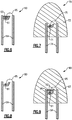
- Fig. 5 depicts a packaged LED 50 which includes a light emitting diode chip 51 (e.g., according to one of the first, second, third and fourth embodiments described above, with the first element above the active layer structure in the orientation depicted), a lumiphor 52, an encapsulant region 53, a lead frame 54 and a wire 55.
- a light emitting diode chip 51 e.g., according to one of the first, second, third and fourth embodiments described above, with the first element above the active layer structure in the orientation depicted
- a lumiphor 52 e.g., according to one of the first, second, third and fourth embodiments described above, with the first element above the active layer structure in the orientation depicted
- a lumiphor 52 e.g., according to one of the first, second, third and fourth embodiments described above, with the first element above the active layer structure in the orientation depicted
- Fig. 6 is a schematic cross-sectional view of a sixth embodiment according to the present invention.
- Fig. 6 depicts a packaged LED 60 which includes a light emitting diode chip 61 (e.g., according to one of the first, second, third and fourth embodiments described above, with the first element above the active layer structure in the orientation depicted), a lumiphor 62, a lead frame 64 and a wire 65.
- a light emitting diode chip 61 e.g., according to one of the first, second, third and fourth embodiments described above, with the first element above the active layer structure in the orientation depicted
- a lumiphor 62 e.g., according to one of the first, second, third and fourth embodiments described above, with the first element above the active layer structure in the orientation depicted
- lead frame 64 e.g., a lead frame 64 and a wire 65.
- Fig. 7 is a schematic cross-sectional view of a seventh embodiment according to the present invention.
- Fig. 7 depicts a packaged LED 70 which includes a light emitting diode chip 71 (e.g., according to one of the first, second, third and fourth embodiments described above, with the first element above the active layer structure in the orientation depicted), an encapsulant region 73, a lead frame 74 and a wire 75.
- a light emitting diode chip 71 e.g., according to one of the first, second, third and fourth embodiments described above, with the first element above the active layer structure in the orientation depicted
- an encapsulant region 73 e.g., according to one of the first, second, third and fourth embodiments described above, with the first element above the active layer structure in the orientation depicted
- a lead frame 74 e.g., a lead frame 74 and a wire 75.
- Fig. 8 is a schematic cross-sectional view of an eighth embodiment according to the present invention.
- Fig. 8 depicts a packaged LED 80 which includes a light emitting diode chip 81 (e.g., according to one of the first, second, third and fourth embodiments described above, with the first element above the active layer structure in the orientation depicted), a lead frame 84 and a wire 85.
- the side of the first element which faces away from the active layer structure is exposed, i.e., it is in contact with a space which comprises air.
- Fig. 9 is a schematic cross-sectional view of a ninth embodiment according to the present invention.
- Fig. 9 depicts a packaged LED 90 which includes a light emitting diode chip 91 (e.g., according to one of the first, second, third and fourth embodiments described above, with the first element above the active layer structure in the orientation depicted), a lumiphor 92, an encapsulant region 93, a lead frame 94 and a wire 95.
- the embodiment shown in Fig. 9 is similar to the embodiment shown in Fig. 5 , except that in the embodiment shown in Fig. 9 , the lumiphor 92 is spaced from the first element of the light emitting diode chip 91, and a space 96 between the lumiphor 92 and the light emitting diode chip 91 comprises air.
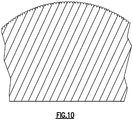
- Fig. 10 is a schematic representation of a surface of a first element which include optical features (not drawn to scale).
- Fig. 10 schematically shows overall curvature of the surface of the first element, as well as micro- or nano- undulations of a moth's eye structure.
- any two or more structural parts of the devices described herein can be integrated. Any structural part of the lighting devices described herein can be provided in two or more parts (which are held together, if necessary). Similarly, any two or more functions can be conducted simultaneously, and/or any function can be conducted in a series of steps.
Description
- The present invention relates to a solid state light emitting device. More particularly, the present invention relates to a solid state light emitting device with improved light extraction efficiency. The present invention also relates to a method of making such solid state light emitting devices.
- A large proportion (some estimates are as high as twenty-five percent) of the electricity generated in the United States each year goes to lighting. Accordingly, there is an ongoing need to provide lighting which is more energy-efficient. It is well-known that incandescent light bulbs are very energy-inefficient light sources - about ninety percent of the electricity they consume is released as heat rather than light. Fluorescent light bulbs are more efficient than incandescent light bulbs (by a factor of about 10) but are still less efficient as compared to solid state light emitters, such as light emitting diodes.
- In addition, as compared to the normal lifetimes of solid state light emitters, e.g., light emitting diodes, incandescent light bulbs have relatively short lifetimes, i.e., typically about 750-1000 hours. In comparison, light emitting diodes, for example, have typical lifetimes between 50,000 and 70,000 hours. Fluorescent bulbs have longer lifetimes (e.g., 10,000 - 20,000 hours) than incandescent lights, but provide less favorable color reproduction.
- Another issue faced by conventional light fixtures is the need to periodically replace the lighting devices (e.g., light bulbs, etc.). Such issues are particularly pronounced where access is difficult (e.g., vaulted ceilings, bridges, high buildings, traffic tunnels) and/or where change-out costs are extremely high. The typical lifetime of conventional fixtures is about 20 years, corresponding to a light-producing device usage of at least about 44,000 hours (based on usage of 6 hours per day for 20 years). Light-producing device lifetime is typically much shorter, thus creating the need for periodic change-outs.
- Accordingly, for these and other reasons, efforts have been ongoing to develop ways by which solid state light emitters can be used in place of incandescent lights, fluorescent lights and other light-generating devices in a wide variety of applications. In addition, where light emitting diodes (or other solid state light emitters) are already being used, efforts are ongoing to provide light emitting diodes (or other solid state light emitters) which are improved, e.g., with respect to energy efficiency, color rendering index (CRI Ra), contrast, efficacy (lm/W), and/or duration of service.
- A variety of solid state light emitters are well-known. For example, one type of solid state light emitter is a light emitting diode.
- Light emitting diodes are semiconductor devices that convert electrical current into light. A wide variety of light emitting diodes are used in increasingly diverse fields for an ever-expanding range of purposes.
- More specifically, light emitting diodes are semiconducting devices that emit light (ultraviolet, visible, or infrared) when a potential difference is applied across a p-n junction structure. There are a number of well-known ways to make light emitting diodes and many associated structures, and the present invention can employ any such devices. By way of example, Chapters 12-14 of Sze, Physics of Semiconductor Devices, (2d Ed. 1981) and Chapter 7 of Sze, Modem Semiconductor Device Physics (1998) describe a variety of photonic devices, including light emitting diodes.
- The expression "light emitting diode" is used herein to refer to the basic semiconductor diode structure (i.e., the chip). The commonly recognized and commercially available "LED" that is sold (for example) in electronics stores typically represents a "packaged" device made up of a number of parts. These packaged devices typically include a semiconductor based light emitting diode such as (but not limited to) those described in
U.S. Pat. Nos. 4,918,487 ;5,631,190 ; and5,912,477 ; various wire connections, and a package that encapsulates the light emitting diode. - As is well-known, a light emitting diode produces light by exciting electrons across the band gap between a conduction band and a valence band of a semiconductor active (light-emitting) layer. The electron transition generates light at a wavelength that depends on the band gap. Thus, the color of the light (wavelength) emitted by a light emitting diode depends on the semiconductor materials of the active layers of the light emitting diode.
- Although the development of light emitting diodes has in many ways revolutionized the lighting industry, some of the characteristics of light emitting diodes have presented challenges, some of which have not yet been fully met. For example, the emission spectrum of any particular light emitting diode is typically concentrated around a single wavelength (as dictated by the light emitting diode's composition and structure), which is desirable for some applications, but not desirable for others, (e.g., for providing lighting, such an emission spectrum provides a very low CRI Ra).
- Because light that is perceived as white is necessarily a blend of light of two or more colors (or wavelengths), no single light emitting diode has been developed that can produce white light. "White" LED lamps have been produced which have a light emitting diode pixel / cluster formed of respective red, green and blue light emitting diodes. Another "white" LED lamp which has been produced includes (1) a light emitting diode which generates blue light and (2) a luminescent material (e.g., a phosphor) that emits yellow light in response to excitation by light emitted by the light emitting diode, whereby the blue light and the yellow light, when mixed, produce light that is perceived as white light.
- Light emitting diodes can thus be used individually or in any combinations, optionally together with one or more luminescent material (e.g., phosphors or scintillators) and/or filters, to generate light of any desired perceived color (including white). Accordingly, the areas in which efforts are being made to replace existing light sources with light emitting diode light sources, e.g., to improve energy efficiency, color rendering index (CRI Ra), efficacy (lm/W), and/or duration of service, are not limited to any particular color or color blends of light.
- A wide variety of luminescent materials (also known as lumiphors or luminophoric media) are well-known and available to persons of skill in the art. For example, a phosphor is a luminescent material that emits a responsive radiation (e.g., visible light) when excited by a source of exciting radiation. In many instances, the responsive radiation has a wavelength which is different from the wavelength of the exciting radiation. Other examples of luminescent materials include scintillators, day glow tapes and inks which glow in the visible spectrum upon illumination with ultraviolet light.
- Luminescent materials can be categorized as being down-converting, i.e., a material which converts photons to a lower energy level (longer wavelength) or up-converting, i.e., a material which converts photons to a higher energy level (shorter wavelength).
- Inclusion of luminescent materials in LED devices has been accomplished by adding the luminescent materials to a clear or substantially transparent encapsulant material (e.g., epoxy-based, silicone-based, glass-based or metal oxide-based material) as discussed above, for example by a blending or coating process.
- As noted above, "white LED lamps" (i.e., lamps which are perceived as being white or near-white) have been investigated as potential replacements for white incandescent lamps. A representative example of a white LED lamp includes a package of a blue light emitting diode chip, made of indium gallium nitride (InGaN) or gallium nitride (GaN), coated with a phosphor such as YAG. In such an LED lamp, the blue light emitting diode chip produces an emission with a wavelength of about 450 nm, and the phosphor produces yellow fluorescence with a peak wavelength of about 550 nm on receiving that emission. For instance, in some designs, white light emitting diode lamps are fabricated by forming a ceramic phosphor layer on the output surface of a blue light-emitting semiconductor light emitting diode. Part of the blue ray emitted from the light emitting diode chip passes through the phosphor, while part of the blue ray emitted from the light emitting diode chip is absorbed by the phosphor, which becomes excited and emits a yellow ray. The part of the blue light emitted by the light emitting diode which is transmitted through the phosphor is mixed with the yellow light emitted by the phosphor. The viewer perceives the mixture of blue and yellow light as white light.
- Another type uses a blue or violet light emitting diode chip which is combined with phosphor materials that produce red or orange and green or yellowish-green light rays. In such a lamp, part of the blue or violet light emitted by the light emitting diode chip excites the phosphors, causing the phosphors to emit red or orange and yellow or green light rays. These rays, combined with the blue or violet rays, can produce the perception of white light.
- As also noted above, in another type of LED lamp, a light emitting diode chip that emits an ultraviolet ray is combined with phosphor materials that produce red (R), green (G) and blue (B) light rays. In such an LED lamp, the ultraviolet ray that has been radiated from the light emitting diode chip excites the phosphor, causing the phosphor to emit red, green and blue light rays which, when mixed, are perceived by the human eye as white light. Consequently, white light can also be obtained as a mixture of these light rays.
- In the case of conventional LED packages which include a phosphor, a significant proportion (e.g., in many cases, as much as 20% to 25%) of the excitation light (i.e., light from the LED) is reflected (back scattered) from the phosphor back into the light emitting diode chip/package. Back scattered light which is scattered back into the light emitting diode chip itself has a very low probability of coming out of the chip, and hence, such back scattering results in a system loss of energy.
- In addition, the phosphor converted light is omni-directional, so that in general, 50% of the light is directed back to the LED source.
-
EP 1538682 ,US 2006/0099449 andJP 61096780 US2005/0184298 A1 discloses a white light source having a plate-shaped wavelength conversion layer illuminated by an encapsulated light-emitting diode. - There is an ongoing need for ways to use light emitting diodes in a wider variety of applications, with greater energy efficiency, low cost and with improved efficacy (lm/W).
- The current invention concerns a solid state light emitting device according to claim 1. Further embodiments are set out in the dependent claims.
- In a first aspect, the present invention is directed to a solid state light emitting device comprising a first element and at least one light emitting active layer structure, in which the first element is positioned on the light emitting active layer structure. In this aspect of the present invention, the first element has at least a first region which has an index of refraction gradient.
- The expression "index of refraction gradient", as used herein in connection with a structure (e.g., a layer, a laminate of layers bonded together or a stack of layers), means that the structure has a first side and a second side, a first region including the first side having a first index of refraction, a second region including the second side having a second index of refraction, the first index of refraction being different from the second index of refraction.
- In some embodiments according to this aspect of the present invention, the first element has at least a first region which has a "stepped index of refraction gradient". The expression "stepped index of refraction gradient", as used herein in connection with a structure, means that the structure has at least a first region, a second region, a third region and a fourth region, and that if light is emitted by the light emitting active layer structure and the light passes through the structure, such light would pass through the first region, then the second region, then the third region and then the fourth region in succession, the first region having a first index of refraction, the second region having a second index of refraction, the third region having a third index of refraction, the fourth region having a fourth index of refraction, the first index of refraction being larger than the second index of refraction, the second index of refraction being larger than the third index of refraction, and the third index of refraction being larger than the fourth index of refraction.
- In some embodiments according to this aspect of the present invention, the first element has at least a first region which has a "substantially continuous index of refraction gradient". The expression "substantially continuous index of refraction gradient", as used herein in connection with a structure, means that the structure has at least ten regions, and that if light is emitted by the light emitting active layer structure and the light passes through the structure, the light would pass through each of the ten regions in succession, each successive layer having a lower index of refraction. In some embodiments according to this aspect of the present invention, the graded index of refraction is a continuous monotonically changing function between the respective surfaces.
- In accordance with the present invention, it has been found that by providing a first element which has at least a first region which has an index of refraction gradient (in some cases, a stepped index of refraction gradient, and in some cases a substantially continuous index of refraction gradient), better light extraction efficiency from the light emitting active layer structure can be obtained.
- While not being bound by any theory, it is believed that the reason the first aspect of the present invention (as well as the other aspects of the present invention, described below) achieves improved light extraction efficiency is by reducing the amount of light that is reflected at one or more interfaces where there would otherwise be a larger drop in index of refraction. That is, the present invention seeks to minimize the magnitude of drops in index of refraction as light emitted from the light emitting active layer structure passes from one region to another by making such drops more gradual. In many aspects of the present invention, as described herein, one or more elements are added to structures which would function as light emitting devices without such added structures, where the added structures are provided to minimize the magnitude of drops in index of refraction which would otherwise occur.
- The expression "on", as used herein, to indicate that a first structure is "on" a second structure, means that the first structure and the second structure are both contained in the same overall structure, and are not necessarily in contact with each other. For example, in the expression "the first element is positioned on the light emitting active layer structure" set forth above, the first element and the light emitting active layer structure are both contained in the same overall structure, and are not necessarily in contact with each other. That is, there may be one or more intervening structures between the first element and the light emitting active layer structure, and each adjoining structure is in direct contact with its immediate neighbor (or neighbors where it has neighbors on both sides). As used herein, a statement that a first structure is "on" a second structure is interchangeable with a statement that the second structure is "on" the first structure (i.e., the order in which the structures are recited in such a statement does not imply anything other than that the structures are contained in the same overall structure.
- One representative example of an intervening structure which is positioned between first and second elements (i.e., where the first element is "on" the second element) is a structure comprising a material which has an index of refraction which is similar to the index of refraction of at least one surface of the first element or the index of refraction of at least one surface of the second element. For example, one such intervening structure is a layer of adhesive (having a thickness of more than 1 micrometer) which has an index of refraction which is similar to the index of refraction of a surface of the first element with which the layer of adhesive is in direct contact. The expression "similar index of refraction" as used herein, e.g., in a statement that the index of refraction (n1) of a first structure is "similar to" the index of refraction (n2) of a second structure means that the total reflection as defined by R = ((n1 - n2) / (n1 + n2))2 is less than 0.01.
- The expression "direct contact" (or "in direct contact with"), as used herein, to indicate that a first structure and a second structure are in "direct contact" means that the first structure is on the second structure (and therefore also the second structure is on the first structure) and that there is substantially nothing between the first structure and the second structure. The expression "substantially nothing" means that there is nothing between the first structure and the second structure, or any material (e.g., glue) between the first structure and the second structure has a thickness which is equal to or less than 1 micrometer, preferably less than one quarter of the wavelength of any visible light.
- In some embodiments according to this aspect of the present invention, the device further comprises a second element which is positioned on an opposite side of the light emitting active layer structure relative to the first element, i.e., the light emitting active layer structure has an active layer structure first side and an active layer structure second side, the first element is positioned on the active layer first side, and the active layer second side is positioned on the second element.
- In some embodiments according to this aspect of the present invention, the device further comprises at least one lumiphor, at least a portion of the lumiphor being positioned opposite the first element relative to the light emitting active layer structure, whereby if light is emitted from the light emitting active layer structure and passes through the first element and the lumiphor, such light would pass through the first element before passing through the lumiphor.
- In some embodiments according to this aspect of the present invention, the device further comprises at least one encapsulant region, at least a portion of the encapsulant region being positioned opposite the first element relative to the light emitting active layer structure, whereby if light is emitted from the light emitting active layer structure and passes through the first element and the encapsulant region, such light would pass through the first element before passing through the encapsulant region. In some such embodiments, the device further comprises at least one lumiphor, at least a portion of the lumiphor being positioned between the first element and the encapsulant region, whereby if light is emitted from the light emitting active layer structure and passes through the first element, the lumiphor and the encapsulant region, such light would pass through the first element before passing through the lumiphor and would pass through the lumiphor before passing through the encapsulant region.
- In some embodiments according to this aspect of the present invention, the device further comprises a second element, wherein the second element is positioned on the light emitting active layer structure, and the first element is positioned on the second element.
- In a second aspect, the present invention is directed to a solid state light emitting device comprising at least one light emitting active layer structure, a first element, a second element and at least one lumiphor. In this aspect of the present invention, the light emitting active layer structure has an active layer structure first side and an active layer structure second side, and a first region of the light emitting active layer structure, which includes the active layer structure first side, has an active layer first region index of refraction. The first element is positioned on the active layer structure first side and the second element is positioned on the active layer structure second side. At least a portion of the first element has a first element index of refraction which is lower than the active layer first region index of refraction. At least a portion of the lumiphor is positioned opposite the first element relative to the light emitting active layer structure, whereby if light is emitted from the light emitting active layer structure and passes through the first element and the lumiphor, such light would pass through the first element before passing through the lumiphor.
- Consistent with as mentioned above, the use of the expression "on" in the preceding paragraph, means that the first element, the active layer structure and the second element are contained in the same overall structure, and the first element is not necessarily in direct contact with the active layer structure first side, and the second element is not necessarily in direct contact with the active layer structure second side.
- In a third aspect, the present invention is directed to a solid state light emitting device comprising a solid state light emitting device comprising at least one light emitting active layer structure, a first element, a second element and at least one encapsulant region. In this aspect of the present invention, the light emitting active layer structure has an active layer structure first side and an active layer structure second side. A first region of the light emitting active layer structure, which includes the active layer structure first side, has an active layer first region index of refraction. The first element is positioned on the active layer structure first side, and the second element is positioned on the active layer structure second side. At least a portion of the first element has a first element index of refraction which is lower than the active layer first region index of refraction. At least a portion of the encapsulant region is positioned opposite the first element relative to the light emitting active layer structure, whereby if light is emitted from the light emitting active layer structure and passes through the first element and the encapsulant region, such light would pass through the first element before passing through the encapsulant region.
- In a fourth aspect, the present invention is directed to a solid state light emitting device comprising a solid state light emitting device comprising at least one light emitting active layer structure, a first element and a second element. In this aspect of the present invention, the light emitting active layer structure has an active layer structure first side and an active layer structure second side. A first region of the light emitting active layer structure, which includes the active layer structure first side, has an active layer first region index of refraction. The first element has a first element first side and a first element second side. The first element second side is positioned on the active layer structure first side, and the second element is positioned on the active layer structure second side. An entirety of the first element first side is exposed. At least a portion of the first element has a first element index of refraction which is lower than the active layer first region index of refraction.
- In a fifth aspect, the present invention is directed to a solid state light emitting device comprising a solid state light emitting device comprising at least one light emitting active layer structure, at least one reflective element, a first element and a second element. In this aspect of the present invention, the light emitting active layer structure has an active layer structure first side and an active layer structure second side, and a first region of the light emitting active layer structure which includes the active layer structure first side has an active layer first index of refraction. The reflective element has a reflective element first side and a reflective element second side. The reflective element first side is positioned on the active layer structure second side. The first element is positioned on the active layer structure first side, and the second element is positioned on the reflective element second side. At least a portion of the first element has a first element index of refraction which is lower than the active layer first index of refraction.
- In a sixth aspect, the present invention is directed to a solid state light emitting device comprising a solid state light emitting device comprising at least one light emitting active layer structure, at least one reflective element, a first element and a second element. In this aspect of the present invention, the light emitting active layer structure has an active layer structure first side and an active layer structure second side. The second element has a second element first side and a second element second side. A first region of the light emitting active layer structure which includes the active layer structure first side has an active layer first index of refraction. The first element is positioned on the active layer structure first side, and the second element first side is positioned on the active layer structure second side. At least a portion of the first element has a first element index of refraction which is lower than the active layer first index of refraction. The reflective element is positioned on the second element second side.
- In a seventh aspect, the present invention is directed to a solid state light emitting device comprising a solid state light emitting device comprising at least one light emitting active layer structure, a first element and a second element. In this aspect of the present invention, the light emitting active layer structure has an active layer structure first side and an active layer structure second side. At least a portion of the first element has a first element index of refraction. The second element has a second element first side and a second element second side, the second element second side being positioned on the active layer structure first side. A first region of the second element, which includes the second element first side, has a second element first index of refraction which is higher than the first element index of refraction. The first element is positioned on the second element first side.
- In an eighth aspect, the present invention is directed to a method of making a solid state light emitting device comprising attaching a first element to at least one light emitting active layer structure, at least a first region of the first element having an index of refraction gradient.
- In some embodiments according to this aspect of the present invention, the method further comprises depositing the light emitting active layer structure on a second element before attaching the first element to the light emitting active layer structure, such that the light emitting active layer structure has an active layer structure first side and an active layer structure second side, the first element is positioned on the active layer first side, and the active layer second side is positioned on the second element.
- In a ninth aspect, the present invention is directed to a method of making a solid state light emitting device comprising (1) depositing a light emitting active layer structure on a second element, such that the light emitting active layer structure has an active layer structure first side and an active layer structure second side, (2) attaching a first element to the active layer structure first side, and (3) positioning at least one lumiphor such that at least a portion of the lumiphor is opposite the first element relative to the light emitting active layer structure, whereby if light is emitted from the light emitting active layer structure and passes through the first element and the lumiphor, such light would pass through the first element before passing through the lumiphor. In this aspect of the present invention, at least a portion of the first element has a first element index of refraction which is lower than an index of refraction of a first region of the active layer, which first region includes the active layer structure first side, and the active layer structure second side is on the second element.
- In a tenth aspect, the present invention is directed to a method of making a solid state light emitting device comprising (1) depositing a light emitting active layer structure on a second element, such that the light emitting active layer structure has an active layer structure first side and an active layer structure second side, (2) attaching a first element to the active layer structure first side, and (3) positioning at least one encapsulant region such that at least a portion of the encapsulant region is opposite the first element relative to the light emitting active layer structure. In this aspect of the present invention, at least a portion of the first element has a first element index of refraction which is lower than an index of refraction of a first region of the active layer, which first region includes the active layer structure first side, and the active layer structure second side is on the second element.
- In some embodiments according to the tenth aspect of the present invention, the method further comprises depositing the second element on at least one reflective element prior to depositing the light emitting active layer structure on the second element, such that the reflective element and the light emitting active layer structure are positioned on opposite sides of the second element.
- In some embodiments according to the tenth aspect of the present invention, the method further comprises depositing at least one reflective element on the second element after depositing the light emitting active layer structure on the second element, such that the reflective element and the light emitting active layer structure are positioned on opposite sides of the second element.
- In an eleventh aspect, the present invention is directed to a method of making a solid state light emitting device, comprising (1) depositing a reflective element on a second element, such that the reflective element has a reflective element first side and a reflective element second side, with the reflective element second side being on the second element (2) depositing a light emitting active layer structure on the reflective element first side, such that the light emitting active layer structure has an active layer structure first side and an active layer structure second side, with the active layer structure second side being on the reflective element first side, and (3) attaching a first element to the active layer structure first side. In this aspect of the present invention, at least a portion of the first element has a first element index of refraction which is lower than an index of refraction of a first region of the active layer, which first region includes the active layer structure first side.
- In a twelfth aspect, the present invention is directed to a method of making a solid state light emitting device comprising (1) depositing a light emitting active layer structure on a second element, such that the light emitting active layer structure has an active layer structure first side and an active layer structure second side, with the active layer structure second side being on the second element (2) attaching a third element to the active layer structure first side, such that the third element has a third element first side and a third element second side, with the third element second side being on the active layer structure first side, (3) removing the second element, and (4) attaching a first element to the active layer structure second side. In this aspect of the present invention, at least a portion of the first element has a first element index of refraction which is lower than an index of refraction of a first region of the active layer structure, which first region includes the active layer structure second side.
- In some embodiments according to the twelfth aspect of the present invention, the method further comprises depositing a reflective material onto the active layer structure first side prior to the attaching a third element to the active layer structure first side, such that the reflective material is positioned between the active layer structure first side and the third element.
- In a thirteenth aspect, the present invention is directed to a method of making a solid state light emitting device comprising:
- depositing a light emitting active layer structure on a first side of a second element, the second element comprising the first side and a second side, such that the light emitting active layer structure has an active layer structure first side and an active layer structure second side, a first region of the light emitting active layer structure which includes the active layer structure first side having an active layer first region index of refraction, the active layer structure first side being on the second element; and
- attaching a first element to the second side of the second element, at least a portion of the first element having a first element index of refraction, the first element index of refraction being lower than the active layer first region index of refraction.
- The invention may be more fully understood with reference to the accompanying drawings and the following detailed description of the invention.
-
-
Fig. 1 is a schematic cross-sectional illustration of a first embodiment according to the present invention. -
Fig. 2 is a schematic cross-sectional illustration of a second embodiment according to the present invention. -
Fig. 3 is a schematic cross-sectional illustration of a third embodiment according to the present invention. -
Fig. 4 is a schematic cross-sectional illustration of a fourth embodiment according to the present invention. -
Fig. 5 is a schematic cross-sectional view of a fifth embodiment according to the present invention. -
Fig. 6 is a schematic cross-sectional view of a sixth embodiment according to the present invention. -
Fig. 7 is a schematic cross-sectional view of a seventh embodiment according to the present invention. -
Fig. 8 is a schematic cross-sectional view of an eighth embodiment according to the present invention. -
Fig. 9 is a schematic cross-sectional view of a ninth embodiment according to the present invention. -
Fig. 10 is a schematic representation of a surface of a first element which include optical features (not drawn to scale). - As noted above, the devices according to the present invention, comprise a first element and at least one light emitting active layer structure, and in various aspects and specific embodiments of the present invention, there can further be provided any additional desired structures, e.g., a second element, one or more lumiphors, one or more encapsulant regions, one or more reflective elements, and/or a third element.
- Generally any suitable material can be used to form the first element, and persons of skill in the art are familiar with a variety of suitable materials. Preferably, the material in the first element is substantially transparent, i.e., if light emitted from the light emitting active layer structure is directed at the first element, at least 95 % of the light across the spectrum of the output from the light emitting active layer structure would pass through the first element. For example, a wide variety of transparent materials can provide the necessary functions for the first element, such as high refractive index glasses, sapphire, a wide variety of crystals, glues, resins, epoxies, silicones, plastics, gels, liquids, air-gels, etc. A representative example of a suitable material is LAH80 glass material from Ohara Corporation, or ZnO with a refractive index of approximately 2.
- The first element can generally be any suitable structure. Persons of skill in the art are readily familiar with a wide variety of such structures, and can readily obtain and/or construct such structures. Any such structures are suitable for use according to the present invention. As noted above, in some aspects and embodiments of the present invention, the first element has an index of refraction gradient (as defined above), and in some embodiments of the present invention, the first element has a stepped index of refraction gradient (as defined above), and in some embodiments of the present invention, the first element has a substantially continuous index of refraction gradient (as defined above).
- Persons of skill in the art can readily obtain or produce structures made of materials suitable for use as the first element which have an index of refraction gradient, a stepped index of refraction gradient and/or a substantially continuous index of refraction gradient, in order to provide a first element for use according to the present invention. For example, persons of skill in the art are familiar with methods of adding two or more glass formulations to each other in order to grade the refractive index. Alternatively or additionally, if desired, ion implantation could be used to provide the index of refraction gradient. Alternatively or additionally, if desired, nano materials including particles, rods or platelets, for example titanium dioxide nanoparticles, can be mixed or embedded in the material to increase, decrease the index of refraction or create a gradient of refractive index.
- In some embodiments of the present invention, the first element has an index of refraction which is lower than the index of refraction of the first region (defined above) of the active layer structure or which is lower than the index of refraction of the first region of the second element. Persons of skill in the art are familiar with a wide variety of suitable materials which can be used for the first element, as well as for the active layer structure and for the second element, as discussed below, and can readily select suitable respective structures whereby the first element has an index of refraction which is lower than the index of refraction of the first region (defined above) of the active layer structure and/or lower than the index of refraction of the first region of the second element.
- In some embodiments of the present invention, one or more luminescent material (e.g., YAG:Ce) can be dispersed (uniformly or non-uniformly) within the first element (in some cases, doing so can eliminate the need for a lumiphor).
- In some embodiments of the present invention, a surface of the first element which is opposite a surface of the first element which is on the active layer structure includes optical features. Persons of skill in the art are familiar with LED packages which have a domed optical surface in order to reduce the effect of total internal reflection. By having a curved surface of the proper radius of curvature, the issue of "critical angle of total internal reflection (TIR)" can be reduced or eliminated. Included in the present invention is the consideration of shaping the exit side (the side exposed to air or the next media of lower index of refraction. Representative examples of such include a macroscopic array of hemispheres of a particular radius, the radius being determined by the endpoints (starting surface and terminating surface) of index of refraction. Or, these shapes could consist of a truly microscopic or nanoscopic array that replicates the "moth eye", such structures, and their manufacture, being familiar to, and readily practiced by, persons of skill in the art.
- Owing to the fact that the first element is attached to a light emitting active layer structure (e.g., sapphire-based, or SiC-based, III-V, IV or II-VI, etc. active layer) to improve light extraction, the "shaping" of the exit surface can be performed with methods that may not be directly compatible with the active layer structure, because the first element is attached to the wafer during a later stage of fabrication, i.e, the process windows are more open.
- Persons of skill in the art are very familiar with methods for determining appropriate radii of curvature for optical features, depending on the respective indices of refraction of the respective materials on either side of the interface between (1) the first element and (2) the structure (e.g., air) with which it is in contact or the fluid (e.g., air) with which it interfaces..
- Such optical features can assist in reducing the index of refraction drop between a surface of the first element which is in direct contact with an encapsulation region and such encapsulation region, or between a surface of the first element which is exposed to air and such air.
- The light emitting active layer structure can generally be any suitable light emitting active layer structure, a wide variety of which are known by those of skill in the art and are readily available. Any such light emitting active layer structure are suitable for use according to the present invention.
- Such light emitting active layer structures include inorganic and organic light emitters. Examples of types of such light emitters include a wide variety of light emitting diodes (inorganic or organic, including polymer light emitting diodes (PLEDs)), laser diodes, thin film electroluminescent devices, light emitting polymers (LEPs), which emit visible light, ultraviolet light and/or infrared light, a variety of each of which are well-known in the art (and therefore it is not necessary to describe in detail such devices, and/or the materials out of which such devices are made).
- The second element (if employed) can generally be any suitable structure. For example, the second element can be any structure commonly referred to as a substrate. Persons of skill in the art are readily familiar with a wide variety of such structures, and can readily obtain and/or construct such structures. Any such structures are suitable for use according to the present invention. Representative examples of materials which can be used to make the second element are gallium phosphide, silicon carbide and silicon (all of which are semi-conductors, but can be electrically conductive), and sapphire (which is electrically non-conductive).
- As noted above, in some embodiments according to the present invention, there is provided one or more reflective elements. Such reflective elements, if employed, can be made of any of a wide variety of suitable reflective elements. For example, representative examples of suitable materials for making the reflective elements include aluminum and silver. There also exist some dielectric reflective elements - if such a reflective element is employed and is deposited directly on a structure which includes one or more contacts, the contacts can, if desired, be masked while depositing the dielectric reflective element or any dielectric material covering a contact can be removed in a later procedure.
- The third element (if employed) can generally be any suitable structure. For example, the third element can be any structure commonly referred to as a substrate. Persons of skill in the art are readily familiar with a wide variety of such structures, and can readily obtain and/or construct such structures. Any such structures are suitable for use according to the present invention. Representative examples of materials which can be used to make the third element are germanium, silicon carbide and silicon.
- Preferably, the devices according to the present invention include contacts through which power can readily be supplied to the light emitting active layer structure(s) to cause the light emitting active layer structure(s) to emit light. Persons of skill in the art are familiar with materials for use in forming contacts, as well as ways to provide such contacts, and any such materials and ways can be employed according to the present invention. Where a layer which is in contact with one side of a light emitting active layer structure is conductive (or where each member of a sequence of layers is conductive, with one of the layers in the sequence being in contact with the light emitting active layer structure), a contact can be provided on the conductive layer (or on any one of the conductive layers in the sequence of layers). Where one or more layer is not conductive (or not deemed to be sufficiently conductive), a one or more contacts can be provided which extends through such non-conductive layer (or insufficiently conductive layer), if necessary, and persons of skill in the art are readily familiar with ways to provide such contacts. Such contacts can be provided at any desired location and in any desired orientation, e.g., either or both contacts can be provided at (and/or extend to) the top and bottom of a laminate of layers which includes the light emitting active layer structure, either or both contacts can be provided (and/or extend) laterally from the light emitting active layer structure (i.e., in a direction parallel to a major surface of the light emitting active layer structure), or any other suitable location, orientation or shape, so long as current can be conducted to and from the light emitting active layer structure.
- Any suitable structure can be provided for electrically connecting to the contacts, and/or for supporting the light emitting device of the present invention. For example, a variety of lead frame structures are well-known to those of skill in the art, and any of such structures may be made in any conventional configuration using any conventional techniques. Such a lead frame is preferably made of metal and may be stamped and optionally post-plated.
- Some embodiments of the present invention comprise a first element, a light emitting active layer structure, a second element and at least two lumiphors, wherein the respective structures are arranged in succession: the first lumiphor, the second layer, the light emitting active layer structure, the first layer and the second lumiphor (with or without any additional layers positioned between any of these layers). Such embodiments can be used as omnidirectional light emitters, i.e., they can generate light and send the light in two opposite directions. In such embodiments, it is preferable that the second element have an index of refraction which is either a gradient or which has a value which is less than the index of refraction of the active layer structure and greater than the index of refraction of the first lumiphor (sapphire is a useful material for constructing such a second element).
- As indicated above, the devices according to the present invention can comprise one or more lumiphors and/or one or more encapsulant regions. Accordingly, the present invention encompasses (but is not limited to):
- (1) devices in which at least some of the light emitted by a light emitting active layer structure passes across an interface between the light emitting active layer structure and a first element, then through the first element, then across an interface between the first element and a lumiphor, then through the lumiphor, then across an interface between the lumiphor and an encapsulant region, then through the encapsulant region and then across an interface between the encapsulant region and the surrounding medium (e.g., air);
- (2) devices in which at least some of the light emitted by a light emitting active layer structure passes across an interface between the light emitting active layer structure and a first element, then through the first element, then across an interface between the first element and an encapsulant region, then through the encapsulant region and then across an interface between the encapsulant region and the surrounding medium (e.g., air);
- (3) devices in which at least some of the light emitted by a light emitting active layer structure passes across an interface between the light emitting active layer structure and a first element, then through the first element, then across an interface between the first element and a lumiphor, then through the lumiphor, then across an interface between the lumiphor and the surrounding medium (e.g., air); and
- (4) devices in which at least some of the light emitted by a light emitting active layer structure passes across an interface between the light emitting active layer structure and a first element, then through the first element, then across an interface between the first element and the surrounding medium (e.g., air).
- A representative typical value for the index of refraction of a GaN or InGaN light emitting active layer structure is from about 2.2 to about 2.3, and that of AlInGaP, AlGaAs, GaP and GaAs is from about 3.2 to about 3.6.
- A representative typical value for the index of refraction of a conventional lumiphor is about 1.8.
- A representative typical value for the index of refraction of a conventional encapsulant region is from about 1.4 to about 1.55 (e.g., for an epoxy encapsulant).
- The index of refraction of air is about 1.0.
- The index of refraction of sapphire, a material which is sometimes used as a substrate for a light emitting device, is about 1.8.
- The index of refraction of SiC, a material which is sometimes used as a substrate for a light emitting device, is about 2.6.
- In accordance with the present invention, there is provided a first element (1) which has an index of refraction gradient (which can be a stepped index of refraction gradient, and/or which can be a substantially continuous index of refraction gradient), and/or (2) at least a portion of which having a first element index of refraction which is lower than the index of refraction of a first region of the active layer. By providing such a first element in a location as described herein, the amount of light internally reflected due to difference in the index of refraction between the structures which are on opposite sides of the first element is reduced as compared with what would be internally reflected if the first element were not positioned between such structures (e.g., instead of the index of refraction changing abruptly from 2.2 to 1.8 as light emitted from the light emitting active layer structure passes from an active layer structure to a lumiphor, the index of refraction drops more gradually as the light passes from the active layer structure into the first element, and then from the first element into the lumiphor. For example, in some embodiments of the present invention, the first element is positioned between and in direct contact with the active layer structure on one side and a lumiphor on the other side, and the first element has a substantially continuous index of refraction gradient ranging from the index of refraction for the active layer structure in the region thereof which includes a surface which is in direct contact with one side of the first element (in a region of the first element which includes the surface of the first element which is in direct contact with the active layer structure) to the index of refraction of a region of the lumiphor which includes a surface which is in direct contact with the other side of the first element (in a region of the first element which includes the surface of the first element which is in direct contact with the lumiphor), e.g., the index of refraction gradient can range from approximately equal to or greater than 2.2 to approximately equal to or less than 1.8. In some embodiments, the first element has an index of refraction which is substantially the geometric mean between the respective indices of refraction of the two materials between which it is positioned (and/or with which it is in contact on its opposite sides), and/or the first element has a refractive index between the respective indices of refraction of the two materials between which it is positioned (and/or with which it is in contact on its opposite sides), such as ZnO with a refractive index of approximately 2.0.
- In other embodiments of the present invention, the first element is positioned between and in direct contact with the active layer structure on one side and an encapsulation region on the other side, and the first element has a substantially continuous index of refraction gradient ranging from the index of refraction for the active layer structure in the region thereof which includes a surface which is in direct contact with one side of the first element (in a region of the first element which includes the surface of the first element which is in direct contact with the active layer structure) to the index of refraction of a portion of the encapsulation region which includes a surface which is in direct contact with the other side of the first element (in a region of the first element which includes the surface of the first element which is in direct contact with the encapsulation region), e.g., the index of refraction gradient ranges from 2.2 to 1.4.
- In other embodiments of the present invention, a first side of the first element is in direct contact with the active layer structure, and a second side of the first element is exposed to air. In some such embodiments, the first element includes an index of refraction gradient which decreases from the first side to the second side, whereby the index of refraction drop between the surface of the first element which is exposed to air and such air is less than the index of refraction drop would be if the active layer structure were exposed to air.
- As noted above, in some embodiments according to the present invention, the lighting device further comprises at least one lumiphor (i.e., luminescence region or luminescent element which comprises at least one luminescent material).
- The one or more lumiphors, when provided, can individually be any lumiphor, a wide variety of which are known to those skilled in the art. For example, the one or more luminescent materials in the lumiphor can be selected from among phosphors, scintillators, day glow tapes, inks which glow in the visible spectrum upon illumination with ultraviolet light, etc. The one or more luminescent materials can be down-converting or up-converting, or can include a combination of both types. For example, the first lumiphor can comprise one or more down-converting luminescent materials.
- The or each of the one or more lumiphors can, if desired, further comprise (or consist essentially of, or consist of) one or more highly transmissive (e.g., transparent or substantially transparent, or somewhat diffuse) binder, e.g., made of epoxy, silicone, glass, metal oxide or any other suitable material (for example, in any given lumiphor comprising one or more binder, one or more phosphor can be dispersed within the one or more binder). For example, the thicker the lumiphor, in general, the lower the weight percentage of the phosphor can be. Representative examples of the weight percentage of phosphor include from about 3.3 weight percent up to about 20 weight percent, although, as indicated above, depending on the overall thickness of the lumiphor, the weight percentage of the phosphor could be generally any value, e.g., from 0.1 weight percent to 100 weight percent (e.g., a lumiphor formed by subjecting pure phosphor to a hot isostatic pressing procedure or electrophoretic deposition process).
- Devices in which a lumiphor is provided can, if desired, further comprise one or more clear encapsulant (comprising, e.g., one or more silicone materials) positioned between the light emitting active layer structure (e.g., light emitting diode) and the lumiphor.
- The, or each of the, one or more lumiphors can, independently, further comprise any of a number of well-known additives, e.g., diffusers, scatterers, tints, refractive index modifying nanoparticles, etc.
- The, or each of the, one or more lumiphors can, independently, be positioned in any desired location, and can be held in place in any desired way, a wide variety of which will be readily apparent to persons of skill in the art, who will be readily able to position such lumiphor(s) in any such manner.
- As noted above, some embodiments according to the present invention comprise one or more encapsulant regions. Persons of skill in the art are familiar with, and have easy access to, a wide variety of materials which are suitable for use in making an encapsulant region for a light emitting device (e.g., LEDs), and any such materials can, if desired, be employed. For example, two well-known representative classes of materials out of which the encapsulant region can be constructed include epoxies and silicones. In addition, any suitable liquid, gas, gel or solid (or combination such as air-gel) which is substantially transparent can be used.
- Persons of skill in the art are also familiar with a wide variety of suitable shapes for the encapsulant region, and the encapsulant region(s)(if employed) in the devices according to the present invention can be of any such shape. Persons of skill in the art are also familiar with various ways to make a packaged device incorporating the various elements described herein in connection with the present invention. Accordingly, further description of materials for use in making the encapsulant region, shapes for the encapsulant region and methods of making the devices described herein is not needed.
- The, or each of the, one or more encapsulant regions can, independently, be positioned in any desired location, and can be held in place in any desired way, a wide variety of which will be readily apparent to persons of skill in the art, who will be readily able to position such encapsulant region(s) in any such manner. The encapsulant regions can, if desired, be formed around other components of the device (e.g., the active layer structure, the first element, the second element, and the one or more lumiphor, if provided) in any of a variety of ways well-known to those skilled in the art. The encapsulant can also be positioned within an enclosure, such as a glass or plastic bubble.
- The structures according to the present invention, as described herein, make it possible to minimize, reduce or eliminate the backscattering of light from the LED by structures within the device, e.g., the light converting layer (such as a lumiphor).
- As noted above, the methods according to the present invention can, if desired, comprise one or more of the following:
- attaching a first element to at least one light emitting active layer structure;
- depositing a light emitting active layer structure on a second element;
- depositing a light emitting active layer structure on a reflective element;
- depositing a second element on at least one reflective element;
- removing a second element;
- positioning at least one lumiphor;
- forming (or positioning) at least one encapsulant region;
- depositing at least one reflective element on a second element;
- depositing a reflective material onto an active layer structure; and
- attaching a third element to an active layer structure first side.
- In general, it is desirable to perform the operations which must be performed at a higher temperature before all operations which can be performed at a lower temperature.
- In many cases, it is desirable to construct wafers having the respective desired structures as described above, e.g., comprising an active layer structure, a first element, a second element (if included), a third element (if included), and one or more reflective elements (if included), and then to dice the wafers into individual die elements (after which one or more lumiphors (if included) and/or one or more encapsulant regions (if included) can be associated with the individual die elements). Persons of skill in the art are familiar with many different methods of dicing, and can readily apply the present invention to the construction of wafers and subsequent dicing. In general, it is preferred to introduce as many of the structures (to be included in the final dice) as possible before performing the dicing operation.
- As noted above, according to some embodiments of the present invention, the first element is attached to at least one light emitting active layer structure. As used herein, the expression "attached", e.g., where a first structure is (or is being) attached to a second structure, means that something which includes (or consists of) the first structure is attached to something which includes (or consists of) the second structure (or that something which includes or consists of the first structure is being attached to something which includes or consists of the second structure. That is, if element one is attached to element two, there might be additional structures (e.g., one or more adhesive layer) positioned between element one and element two (likewise, if element one is being attached to element two, there might be additional structures, e.g., one or more adhesive layer, positioned between element one and element two after element one becomes attached to element two). As used herein, the expression "attached", e.g., where a first structure is being attached to a second structure, encompasses bonding the first structure to the second structure (e.g., by applying an adhesive to the second layer and then bringing the first layer into contact with the adhesive) or bonding the second structure to the first structure (or, where a first structure is attached to a second structure, the first structure bonded to the second structure, e.g., with an adhesive between the second layer and the first layer). As used herein, a statement that a first structure is being attached to a second structure is interchangeable with a statement that the second structure is being attached to the first structure (i.e., the order in which the structures are recited in such a statement does not imply anything other than that the structures end up being attached at the end of the procedure). Further, as used herein, the expressions "attaching" and "attached" encompass depositing one structure upon another ("depositing" is discussed in more detail below), e.g., a statement that a first structure is being attached to a second structure encompasses depositing the first structure on the second structure or depositing the second structure on the first structure. In addition, as used herein, the expressions "positioning" and "positioned" encompass depositing one structure upon another ("depositing" is discussed in more detail below), e.g., the expression "positioning" a structure encompasses depositing the structure. A statement that a first structure is directly attached to a second structure (which falls within the scope of attaching a first structure to a second structure) means that after the attaching is completed, the first structure and second structure are attached to each other and are in direct contact with each other.
- The first element can be attached to the at least one light emitting active layer structure in any suitable way, a variety of which are familiar to, and can readily be carried out by, those of skill in the art. For example, the first element can be attached using van der Waals bonding, covalent bonding, electrostatic bonding (e.g., using heat, pressure and/or electric charge), applying glue, etc. Additionally, the first element can be deposited onto the at least one light emitting active layer structure in any suitable way, a variety of which are familiar to, and can readily be carried out by, those of skill in the art. For example, the first element can be deposited using pulsed laser deposition PLD.
- As described above, various structures can be deposited. As used herein, the expression "deposited", e.g., where a first structure is being deposited on a second structure, means that something which includes (or consists of) the first structure is being directly deposited on something which includes (or consists of) the second structure. That is, if element one is being deposited on element two, there might be additional structures positioned between element one and element two after element one becomes deposited on element two. A statement that a first structure is directly deposited on a second structure (which falls within the scope of depositing a first structure on a second structure) means that after the depositing is completed, the first structure and second structure are in direct contact with each other.
- Persons of skill in the art are very familiar with a variety of processes for depositing one material onto another, particularly in the context of constructing a solid state light emitting device, and skilled artisans would readily be able to perform such depositing procedures.
- A second element can be removed in any suitable way, a wide variety of which are familiar to persons of skill in the art. For example, any of a wide variety of etching procedures can be employed.
- The devices of the present invention can be arranged, mounted and supplied with electricity in any desired manner, and can be mounted on any desired housing or fixture. Skilled artisans are familiar with a wide variety of arrangements, mounting schemes, power supplying apparatuses, housings and fixtures, and any such arrangements, schemes, apparatuses, housings and fixtures can be employed in connection with the present invention. The lighting devices of the present invention can be electrically connected (or selectively connected) to any desired power source, persons of skill in the art being familiar with a variety of such power sources.
- In some embodiments according to the present invention, one or more of the light emitting diodes can be included in a package together with one or more of the lumiphors, and the one or more lumiphor in the package can be spaced from the one or more light emitting diode in the package to achieve improved light extraction efficiency.
- In some embodiments according to the present invention, two or more lumiphors can be provided, two or more of the lumiphors being spaced from each other.
-
Fig. 1 is a schematic cross-sectional illustration of a first embodiment according to the present invention. Referring toFig. 1 , there is shown alight emitter 10 including afirst element 11, a light emittingactive layer structure 12, asecond element 13, acontact 14 and a metallized contact 15. Thefirst element 11, the light emittingactive layer structure 12, and thesecond element 13 are each generally rectilinear, i.e., a top view of any of them would show a generally rectangular perimeter. - In this embodiment, the first element is in direct contact with the light emitting active layer structure.
- In this embodiment, the light emitting active layer structure has an active layer structure
first side 16 and an active layer structuresecond side 17. Thefirst element 11 is positioned on (and in direct contact with) the active layer structurefirst side 16, and the active layersecond side 17 is positioned on (and in direct contact with) thesecond element 13. Also are included electricallyconductive contacts 14 and 15. -
Fig. 2 is a schematic cross-sectional illustration of a second embodiment according to the present invention. Referring toFig. 2 , there is shown alight emitter 20 including afirst element 21, a light emittingactive layer structure 22, areflective element 28, asecond element 23, an electricallyconductive contact 24 and an electrically conductive contact 25. - In this embodiment, the first element is in direct contact with the light emitting active layer structure.
- In this embodiment, the light emitting active layer structure has an active layer structure
first side 26 and an active layer structuresecond side 27. To illustrate the terminology described above, thefirst element 21 is positioned on (and in direct contact with) the active layer structure first side 26 (and vice-versa), the active layersecond side 27 is positioned on (but not in direct contact with) the second element 23 (and vice-versa), thereflective layer 28 is positioned on (and in direct contact with) the second element 23 (and vice-versa), and the light emittingactive layer structure 22 is positioned on (and in direct contact with) the reflective layer 28 (and vice-versa, i.e., thereflective layer 28 is positioned on and in direct contact with the light emitting active layer structure 22). -
Fig. 3 is a schematic cross-sectional illustration of a third embodiment according to the present invention. Referring toFig. 3 , there is shown alight emitter 30 including afirst element 31, a light emittingactive layer structure 32, asecond element 33, a firstreflective layer 38, a secondreflective layer 39, an electricallyconductive contact 34 and an electricallyconductive contact 35. The secondreflective layer 39 goes around the entire circumference of thesecond element 33. The angle of the beveled secondreflective layer 39, relative to a vertical (in the orientation shown inFig. 3 ) line is preferably not larger than 45 degrees. In this embodiment, one method of providing the beveled mirrors is to perform partial cuts in the wafer to provide beveled grooves, then metallize the grooves, and then complete the cutting (i.e., to divide the wafer into a plurality of dice). -
Fig. 4 is a schematic cross-sectional illustration of a fourth embodiment according to the present invention. Referring toFig. 4 , there is shown a light emitter 40 including a first element 41, a light emitting active layer structure 42, asecond element 43, an electricallyconductive contact 44 and an electricallyconductive contact 45. This embodiment can optionally further include a reflective element positioned on the active layer structure 42 opposite thesecond element 43, and/or one or more beveled reflective elements analogous to as shown inFig. 3 . -
Fig. 5 is a schematic cross-sectional view of a fifth embodiment according to the present invention.Fig. 5 depicts a packagedLED 50 which includes a light emitting diode chip 51 (e.g., according to one of the first, second, third and fourth embodiments described above, with the first element above the active layer structure in the orientation depicted), alumiphor 52, anencapsulant region 53, a lead frame 54 and awire 55. -
Fig. 6 is a schematic cross-sectional view of a sixth embodiment according to the present invention.Fig. 6 depicts a packagedLED 60 which includes a light emitting diode chip 61 (e.g., according to one of the first, second, third and fourth embodiments described above, with the first element above the active layer structure in the orientation depicted), alumiphor 62, alead frame 64 and awire 65. -
Fig. 7 is a schematic cross-sectional view of a seventh embodiment according to the present invention.Fig. 7 depicts a packagedLED 70 which includes a light emitting diode chip 71 (e.g., according to one of the first, second, third and fourth embodiments described above, with the first element above the active layer structure in the orientation depicted), anencapsulant region 73, alead frame 74 and awire 75. -
Fig. 8 is a schematic cross-sectional view of an eighth embodiment according to the present invention.Fig. 8 depicts a packagedLED 80 which includes a light emitting diode chip 81 (e.g., according to one of the first, second, third and fourth embodiments described above, with the first element above the active layer structure in the orientation depicted), a lead frame 84 and awire 85. In this embodiment, the side of the first element which faces away from the active layer structure is exposed, i.e., it is in contact with a space which comprises air. -
Fig. 9 is a schematic cross-sectional view of a ninth embodiment according to the present invention.Fig. 9 depicts a packagedLED 90 which includes a light emitting diode chip 91 (e.g., according to one of the first, second, third and fourth embodiments described above, with the first element above the active layer structure in the orientation depicted), alumiphor 92, anencapsulant region 93, a lead frame 94 and awire 95. The embodiment shown inFig. 9 is similar to the embodiment shown inFig. 5 , except that in the embodiment shown inFig. 9 , thelumiphor 92 is spaced from the first element of the light emittingdiode chip 91, and aspace 96 between the lumiphor 92 and the light emittingdiode chip 91 comprises air. - Persons of skill in the art are familiar with, and are able to practice, a variety of methods for making packaged LEDs, and any such methods can be employed to make packaged LEDs according to the present invention.
Fig. 10 is a schematic representation of a surface of a first element which include optical features (not drawn to scale).Fig. 10 schematically shows overall curvature of the surface of the first element, as well as micro- or nano- undulations of a moth's eye structure. - Any two or more structural parts of the devices described herein can be integrated. Any structural part of the lighting devices described herein can be provided in two or more parts (which are held together, if necessary). Similarly, any two or more functions can be conducted simultaneously, and/or any function can be conducted in a series of steps.
Claims (10)
- A solid state light emitting device comprising:a light emitting active layer structure (12, 22, 32, 42) having an active layer first side (16, 26) and an active layer second side (17, 27);a first element (11, 21, 31, 41), said first element (11, 21, 31, 41) being a layer and having a first element first side and a first element second side, said first element second side in direct contact with said active layer first side (16, 26); anda lumiphor (52, 62) having a surface in direct contact with said first element first side, wherein the first element does not include a luminescent material, such that, in use, light emitted from the light emitting active layer structure (12, 22, 32, 42) passes through the first element (11, 21, 31, 41) before passing through the lumiphor (52, 62), and the first element (11, 21, 31, 41) has a substantially continuous index of refraction gradient ranging from the index of refraction of the active layer structure in a region of the first element including the first element second side to the index of refraction of a region of the lumiphor in a region of the first element including the first element first side.
- A solid state light emitting device as recited in claim 1, wherein said solid state light emitting device further comprises a second element (13, 23, 33) on said active layer second side (17, 27).
- A solid state light emitting device as recited in claim 2, wherein said solid state light emitting device further comprises at least one reflective element (28) between said second element (23) and said light emitting active layer structure (22).
- A solid state light emitting device as recited in claim 2, wherein:said solid state light emitting device further comprises at least one reflective element (28),said reflective element (28) has a reflective element first side and a reflective element second side,said reflective element first side is on said active layer structure second side (27); andsaid second element (23) is on said reflective element second side.
- A solid state light emitting device as recited in claim 2, wherein:said solid state light emitting device further comprises at least one reflective element (38), andsaid reflective element (38) is on a second side of said second element (33), such that the second element is located between the reflective element and said active layer structure.
- A solid state light emitting device as recited in claim 5, wherein:said solid state light emitting device further comprises at least one bevel reflective element (39),said bevel reflective element (39) is on a second element third side, andsaid second element third side extends between said second element first side and said second element second side.
- A solid state light emitting device as recited in claim 1, wherein:said solid state light emitting device further comprises a second element (43),said second element (43) is on said light emitting active layer structure (42), andsaid first element (41) is on said second element (43).
- A solid state light emitting device as recited in any one of claims 1-7, wherein said first element first side comprises at least one optical feature.
- A solid state light emitting device as recited in any one of claims 1-8, wherein:said solid state light emitting device further comprises at least one encapsulant region (53), andat least a portion of said lumiphor (52) is between said first element (11, 21, 31, 41) and said encapsulant region (53), whereby if light is emitted from said light emitting active layer structure (12, 22, 32, 42) and passes through said first element (11, 21, 31, 41), said lumiphor (52) and said encapsulant region (53), such light would pass through said first element (11, 21, 31, 41) before passing through said lumiphor (52) and would pass through said lumiphor (52) before passing through said encapsulant region (53).
- A solid state lighting device as recited in claim 1, wherein:said solid state light emitting device comprises a second element, a first lumiphor and a second lumiphor,the second element positioned between the first lumiphor and the light emitting active layer structure,the first element positioned between the second lumiphor and the light emitting active layer structure,the first element and the second element on opposite sides of the light emitting active layer structure.
Applications Claiming Priority (2)
| Application Number | Priority Date | Filing Date | Title |
|---|---|---|---|
| US80892506P | 2006-05-26 | 2006-05-26 | |
| PCT/US2007/012403 WO2007139894A2 (en) | 2006-05-26 | 2007-05-24 | Solid state light emitting device and method of making same |
Publications (3)
| Publication Number | Publication Date |
|---|---|
| EP2033235A2 EP2033235A2 (en) | 2009-03-11 |
| EP2033235A4 EP2033235A4 (en) | 2012-05-23 |
| EP2033235B1 true EP2033235B1 (en) | 2017-06-21 |
Family
ID=38779219
Family Applications (1)
| Application Number | Title | Priority Date | Filing Date |
|---|---|---|---|
| EP07795294.3A Active EP2033235B1 (en) | 2006-05-26 | 2007-05-24 | Solid state light emitting device |
Country Status (5)
| Country | Link |
|---|---|
| US (1) | US8008676B2 (en) |
| EP (1) | EP2033235B1 (en) |
| JP (1) | JP2009538536A (en) |
| TW (1) | TWI425652B (en) |
| WO (1) | WO2007139894A2 (en) |
Families Citing this family (102)
| Publication number | Priority date | Publication date | Assignee | Title |
|---|---|---|---|---|
| US7145125B2 (en) | 2003-06-23 | 2006-12-05 | Advanced Optical Technologies, Llc | Integrating chamber cone light using LED sources |
| US7521667B2 (en) | 2003-06-23 | 2009-04-21 | Advanced Optical Technologies, Llc | Intelligent solid state lighting |
| US7355284B2 (en) | 2004-03-29 | 2008-04-08 | Cree, Inc. | Semiconductor light emitting devices including flexible film having therein an optical element |
| US20060097385A1 (en) | 2004-10-25 | 2006-05-11 | Negley Gerald H | Solid metal block semiconductor light emitting device mounting substrates and packages including cavities and heat sinks, and methods of packaging same |
| US8125137B2 (en) | 2005-01-10 | 2012-02-28 | Cree, Inc. | Multi-chip light emitting device lamps for providing high-CRI warm white light and light fixtures including the same |
| US7564180B2 (en) | 2005-01-10 | 2009-07-21 | Cree, Inc. | Light emission device and method utilizing multiple emitters and multiple phosphors |
| US8514210B2 (en) | 2005-11-18 | 2013-08-20 | Cree, Inc. | Systems and methods for calibrating solid state lighting panels using combined light output measurements |
| US7959325B2 (en) * | 2005-11-18 | 2011-06-14 | Cree, Inc. | Solid state lighting units and methods of forming solid state lighting units |
| WO2007061811A1 (en) | 2005-11-18 | 2007-05-31 | Cree, Inc. | Solid state lighting panels with variable voltage boost current sources |
| US7872430B2 (en) | 2005-11-18 | 2011-01-18 | Cree, Inc. | Solid state lighting panels with variable voltage boost current sources |
| EP2372224A3 (en) | 2005-12-21 | 2012-08-01 | Cree, Inc. | Lighting Device and Lighting Method |
| TWI421438B (en) | 2005-12-21 | 2014-01-01 | 克里公司 | Lighting device |
| JP2009527071A (en) | 2005-12-22 | 2009-07-23 | クリー エル イー ディー ライティング ソリューションズ インコーポレイテッド | Lighting device |
| US8441179B2 (en) | 2006-01-20 | 2013-05-14 | Cree, Inc. | Lighting devices having remote lumiphors that are excited by lumiphor-converted semiconductor excitation sources |
| US9084328B2 (en) | 2006-12-01 | 2015-07-14 | Cree, Inc. | Lighting device and lighting method |
| US8998444B2 (en) | 2006-04-18 | 2015-04-07 | Cree, Inc. | Solid state lighting devices including light mixtures |
| US8513875B2 (en) | 2006-04-18 | 2013-08-20 | Cree, Inc. | Lighting device and lighting method |
| US7821194B2 (en) | 2006-04-18 | 2010-10-26 | Cree, Inc. | Solid state lighting devices including light mixtures |
| TWI460880B (en) | 2006-04-18 | 2014-11-11 | Cree Inc | Lighting device and lighting method |
| EP2008019B1 (en) | 2006-04-20 | 2015-08-05 | Cree, Inc. | Lighting device and lighting method |
| WO2007139894A2 (en) | 2006-05-26 | 2007-12-06 | Cree Led Lighting Solutions, Inc. | Solid state light emitting device and method of making same |
| KR20140116536A (en) | 2006-05-31 | 2014-10-02 | 크리, 인코포레이티드 | Lighting device and method of lighting |
| US7665862B2 (en) * | 2006-09-12 | 2010-02-23 | Cree, Inc. | LED lighting fixture |
| US7766508B2 (en) | 2006-09-12 | 2010-08-03 | Cree, Inc. | LED lighting fixture |
| CN101595342B (en) * | 2006-10-23 | 2012-10-24 | 科锐公司 | Lighting devices and methods of installing light engine housings and/or trim elements in lighting device housings |
| US8029155B2 (en) | 2006-11-07 | 2011-10-04 | Cree, Inc. | Lighting device and lighting method |
| TWI496315B (en) | 2006-11-13 | 2015-08-11 | Cree Inc | Lighting device, illuminated enclosure and lighting methods |
| EP2095014B1 (en) | 2006-11-14 | 2017-05-10 | Cree, Inc. | Light engine assemblies |
| US8439531B2 (en) * | 2006-11-14 | 2013-05-14 | Cree, Inc. | Lighting assemblies and components for lighting assemblies |
| WO2008067441A1 (en) | 2006-11-30 | 2008-06-05 | Cree Led Lighting Solutions, Inc. | Lighting device and lighting method |
| US9441793B2 (en) | 2006-12-01 | 2016-09-13 | Cree, Inc. | High efficiency lighting device including one or more solid state light emitters, and method of lighting |
| WO2008070607A1 (en) | 2006-12-04 | 2008-06-12 | Cree Led Lighting Solutions, Inc. | Lighting assembly and lighting method |
| WO2008073794A1 (en) | 2006-12-07 | 2008-06-19 | Cree Led Lighting Solutions, Inc. | Lighting device and lighting method |
| US8258682B2 (en) | 2007-02-12 | 2012-09-04 | Cree, Inc. | High thermal conductivity packaging for solid state light emitting apparatus and associated assembling methods |
| US20080198572A1 (en) | 2007-02-21 | 2008-08-21 | Medendorp Nicholas W | LED lighting systems including luminescent layers on remote reflectors |
| CN101657671B (en) | 2007-02-22 | 2012-07-11 | 科锐公司 | Lighting devices, methods of lighting, light filters and methods of filtering light |
| US7638811B2 (en) * | 2007-03-13 | 2009-12-29 | Cree, Inc. | Graded dielectric layer |
| TWI334660B (en) * | 2007-03-21 | 2010-12-11 | Lextar Electronics Corp | Surface mount type light emitting diode package device and light emitting element package device |
| US7824070B2 (en) | 2007-03-22 | 2010-11-02 | Cree, Inc. | LED lighting fixture |
| WO2008137984A1 (en) | 2007-05-08 | 2008-11-13 | Cree Led Lighting Solutions, Inc. | Lighting devices and methods for lighting |
| BRPI0811561A2 (en) | 2007-05-08 | 2015-06-16 | Cree Led Lighting Solutions | Lighting device and lighting method |
| EP2142844B1 (en) | 2007-05-08 | 2017-08-23 | Cree, Inc. | Lighting device and lighting method |
| KR20100022969A (en) | 2007-05-08 | 2010-03-03 | 크리 엘이디 라이팅 솔루션즈, 인크. | Lighting device and lighting method |
| US8049709B2 (en) | 2007-05-08 | 2011-11-01 | Cree, Inc. | Systems and methods for controlling a solid state lighting panel |
| EP2156090B1 (en) | 2007-05-08 | 2016-07-06 | Cree, Inc. | Lighting device and lighting method |
| EP2142843B1 (en) | 2007-05-08 | 2016-12-14 | Cree, Inc. | Lighting device and lighting method |
| US7863635B2 (en) | 2007-08-07 | 2011-01-04 | Cree, Inc. | Semiconductor light emitting devices with applied wavelength conversion materials |
| EP2210036B1 (en) | 2007-10-10 | 2016-11-23 | Cree, Inc. | Lighting device and method of making |
| US10256385B2 (en) | 2007-10-31 | 2019-04-09 | Cree, Inc. | Light emitting die (LED) packages and related methods |
| US8350461B2 (en) | 2008-03-28 | 2013-01-08 | Cree, Inc. | Apparatus and methods for combining light emitters |
| US8240875B2 (en) | 2008-06-25 | 2012-08-14 | Cree, Inc. | Solid state linear array modules for general illumination |
| US8445824B2 (en) * | 2008-10-24 | 2013-05-21 | Cree, Inc. | Lighting device |
| US8858032B2 (en) * | 2008-10-24 | 2014-10-14 | Cree, Inc. | Lighting device, heat transfer structure and heat transfer element |
| US10197240B2 (en) * | 2009-01-09 | 2019-02-05 | Cree, Inc. | Lighting device |
| US7967652B2 (en) | 2009-02-19 | 2011-06-28 | Cree, Inc. | Methods for combining light emitting devices in a package and packages including combined light emitting devices |
| US8333631B2 (en) | 2009-02-19 | 2012-12-18 | Cree, Inc. | Methods for combining light emitting devices in a package and packages including combined light emitting devices |
| US8950910B2 (en) | 2009-03-26 | 2015-02-10 | Cree, Inc. | Lighting device and method of cooling lighting device |
| US8337030B2 (en) | 2009-05-13 | 2012-12-25 | Cree, Inc. | Solid state lighting devices having remote luminescent material-containing element, and lighting methods |
| US9841162B2 (en) | 2009-05-18 | 2017-12-12 | Cree, Inc. | Lighting device with multiple-region reflector |
| US8921876B2 (en) | 2009-06-02 | 2014-12-30 | Cree, Inc. | Lighting devices with discrete lumiphor-bearing regions within or on a surface of remote elements |
| US8716952B2 (en) | 2009-08-04 | 2014-05-06 | Cree, Inc. | Lighting device having first, second and third groups of solid state light emitters, and lighting arrangement |
| US8648546B2 (en) * | 2009-08-14 | 2014-02-11 | Cree, Inc. | High efficiency lighting device including one or more saturated light emitters, and method of lighting |
| US9605844B2 (en) | 2009-09-01 | 2017-03-28 | Cree, Inc. | Lighting device with heat dissipation elements |
| US10264637B2 (en) | 2009-09-24 | 2019-04-16 | Cree, Inc. | Solid state lighting apparatus with compensation bypass circuits and methods of operation thereof |
| US9713211B2 (en) | 2009-09-24 | 2017-07-18 | Cree, Inc. | Solid state lighting apparatus with controllable bypass circuits and methods of operation thereof |
| US8901845B2 (en) | 2009-09-24 | 2014-12-02 | Cree, Inc. | Temperature responsive control for lighting apparatus including light emitting devices providing different chromaticities and related methods |
| US9464801B2 (en) | 2009-09-25 | 2016-10-11 | Cree, Inc. | Lighting device with one or more removable heat sink elements |
| TW201132740A (en) | 2009-09-25 | 2011-10-01 | Panasonic Elec Works Co Ltd | Wavelength converting particle, wavelength converting member including same, and light-emitting device |
| US9285103B2 (en) | 2009-09-25 | 2016-03-15 | Cree, Inc. | Light engines for lighting devices |
| US8602579B2 (en) | 2009-09-25 | 2013-12-10 | Cree, Inc. | Lighting devices including thermally conductive housings and related structures |
| WO2011037882A2 (en) | 2009-09-25 | 2011-03-31 | Cree, Inc. | Lighting device having heat dissipation element |
| US9068719B2 (en) | 2009-09-25 | 2015-06-30 | Cree, Inc. | Light engines for lighting devices |
| US9353933B2 (en) | 2009-09-25 | 2016-05-31 | Cree, Inc. | Lighting device with position-retaining element |
| WO2011037876A1 (en) | 2009-09-25 | 2011-03-31 | Cree, Inc. | Lighting device having heat dissipation element |
| KR20120094477A (en) | 2009-09-25 | 2012-08-24 | 크리, 인코포레이티드 | Lighting device with low glare and high light level uniformity |
| US8777449B2 (en) | 2009-09-25 | 2014-07-15 | Cree, Inc. | Lighting devices comprising solid state light emitters |
| US9217542B2 (en) | 2009-10-20 | 2015-12-22 | Cree, Inc. | Heat sinks and lamp incorporating same |
| US9030120B2 (en) | 2009-10-20 | 2015-05-12 | Cree, Inc. | Heat sinks and lamp incorporating same |
| US9435493B2 (en) | 2009-10-27 | 2016-09-06 | Cree, Inc. | Hybrid reflector system for lighting device |
| US8604461B2 (en) * | 2009-12-16 | 2013-12-10 | Cree, Inc. | Semiconductor device structures with modulated doping and related methods |
| US8536615B1 (en) | 2009-12-16 | 2013-09-17 | Cree, Inc. | Semiconductor device structures with modulated and delta doping and related methods |
| US8508116B2 (en) | 2010-01-27 | 2013-08-13 | Cree, Inc. | Lighting device with multi-chip light emitters, solid state light emitter support members and lighting elements |
| CN102782391B (en) | 2010-02-12 | 2016-08-03 | 科锐公司 | Solid state illumination device and assembly method thereof |
| US20110267821A1 (en) | 2010-02-12 | 2011-11-03 | Cree, Inc. | Lighting device with heat dissipation elements |
| US8773007B2 (en) | 2010-02-12 | 2014-07-08 | Cree, Inc. | Lighting devices that comprise one or more solid state light emitters |
| US9518715B2 (en) | 2010-02-12 | 2016-12-13 | Cree, Inc. | Lighting devices that comprise one or more solid state light emitters |
| EP2534407A2 (en) | 2010-02-12 | 2012-12-19 | Cree, Inc. | Lighting devices that comprise one or more solid state light emitters |
| US9275979B2 (en) | 2010-03-03 | 2016-03-01 | Cree, Inc. | Enhanced color rendering index emitter through phosphor separation |
| US8476836B2 (en) | 2010-05-07 | 2013-07-02 | Cree, Inc. | AC driven solid state lighting apparatus with LED string including switched segments |
| US8684559B2 (en) | 2010-06-04 | 2014-04-01 | Cree, Inc. | Solid state light source emitting warm light with high CRI |
| US9648673B2 (en) | 2010-11-05 | 2017-05-09 | Cree, Inc. | Lighting device with spatially segregated primary and secondary emitters |
| US8556469B2 (en) | 2010-12-06 | 2013-10-15 | Cree, Inc. | High efficiency total internal reflection optic for solid state lighting luminaires |
| WO2012103292A1 (en) * | 2011-01-26 | 2012-08-02 | Massachusetts Institute Of Technology | Device and method for luminescence enhancement by resonant energy transfer from an absorptive thin film |
| US11251164B2 (en) | 2011-02-16 | 2022-02-15 | Creeled, Inc. | Multi-layer conversion material for down conversion in solid state lighting |
| US9839083B2 (en) | 2011-06-03 | 2017-12-05 | Cree, Inc. | Solid state lighting apparatus and circuits including LED segments configured for targeted spectral power distribution and methods of operating the same |
| US8742671B2 (en) | 2011-07-28 | 2014-06-03 | Cree, Inc. | Solid state lighting apparatus and methods using integrated driver circuitry |
| US9151457B2 (en) | 2012-02-03 | 2015-10-06 | Cree, Inc. | Lighting device and method of installing light emitter |
| US9151477B2 (en) | 2012-02-03 | 2015-10-06 | Cree, Inc. | Lighting device and method of installing light emitter |
| US9279946B2 (en) * | 2012-05-23 | 2016-03-08 | Avago Technologies General Ip (Singapore) Pte. Ltd. | Premolded cavity for optoelectronic device |
| DE102012106984A1 (en) * | 2012-07-31 | 2014-02-06 | Osram Opto Semiconductors Gmbh | Optoelectronic semiconductor component and method for producing an optoelectronic semiconductor component |
| CN104241262B (en) | 2013-06-14 | 2020-11-06 | 惠州科锐半导体照明有限公司 | Light emitting device and display device |
| JP6518936B2 (en) * | 2014-11-14 | 2019-05-29 | パナソニックIpマネジメント株式会社 | Component mounting device |
Citations (1)
| Publication number | Priority date | Publication date | Assignee | Title |
|---|---|---|---|---|
| US20050184298A1 (en) * | 2004-02-19 | 2005-08-25 | Matsushita Electric Industrial Co., Ltd. | White light emitting element and white light source |
Family Cites Families (199)
| Publication number | Priority date | Publication date | Assignee | Title |
|---|---|---|---|---|
| GB1136218A (en) | 1965-12-14 | 1968-12-11 | Standard Telephones Cables Ltd | Improvements in or relating to the manufacture of semiconductor optical devices |
| FR1536293A (en) | 1967-06-22 | 1968-08-16 | Citroen Sa Andre | Improvements made to the layout of the power unit of a motor vehicle |
| JPS48102585A (en) | 1972-04-04 | 1973-12-22 | ||
| US3927290A (en) | 1974-11-14 | 1975-12-16 | Teletype Corp | Selectively illuminated pushbutton switch |
| US4152044A (en) * | 1977-06-17 | 1979-05-01 | International Telephone And Telegraph Corporation | Galium aluminum arsenide graded index waveguide |
| JPS5517180A (en) | 1978-07-24 | 1980-02-06 | Handotai Kenkyu Shinkokai | Light emitting diode display |
| JPS5722581Y2 (en) | 1979-08-21 | 1982-05-17 | ||
| US4476620A (en) | 1979-10-19 | 1984-10-16 | Matsushita Electric Industrial Co., Ltd. | Method of making a gallium nitride light-emitting diode |
| US4427213A (en) | 1982-01-21 | 1984-01-24 | Raidel Jr John E | Vehicle suspension with rigid torque beam |
| NL8301824A (en) | 1983-05-24 | 1984-12-17 | Philips Nv | OPTICAL ELEMENT COMPRISING A TRANSPARENT SUBSTRATE AND ANTI-REFLECTIVE CLOTHING FOR THE WAVE LENGTH AREA IN THE NEAR INFRARED. |
| US4566719A (en) | 1984-02-17 | 1986-01-28 | Turner Quick Lift Corporation | Spaced axle-to-beam connection for suspension of the rigid beam type |
| JPS6196780A (en) | 1984-10-17 | 1986-05-15 | Stanley Electric Co Ltd | Coating method of lead chip |
| US4583822A (en) | 1984-10-31 | 1986-04-22 | Rockwell International Corporation | Quintic refractive index profile antireflection coatings |
| US4890150A (en) | 1985-12-05 | 1989-12-26 | North American Philips Corporation | Dielectric passivation |
| US5002305A (en) | 1987-02-04 | 1991-03-26 | Raidel John E | Vehicle suspension system with standardized torque beam and special monopivot bushing assembly |
| US4934788A (en) | 1987-03-20 | 1990-06-19 | Rockwell International Corporation | Deposition of gradient index coatings using coevaporation with rate control |
| US4866005A (en) | 1987-10-26 | 1989-09-12 | North Carolina State University | Sublimation of silicon carbide to produce large, device quality single crystals of silicon carbide |
| US4981551A (en) | 1987-11-03 | 1991-01-01 | North Carolina State University | Dry etching of silicon carbide |
| US4865685A (en) | 1987-11-03 | 1989-09-12 | North Carolina State University | Dry etching of silicon carbide |
| JPH0770755B2 (en) | 1988-01-21 | 1995-07-31 | 三菱化学株式会社 | High brightness LED epitaxial substrate and method of manufacturing the same |
| US5880510A (en) | 1988-05-11 | 1999-03-09 | Raytheon Company | Graded layer passivation of group II-VI infrared photodetectors |
| US4912532A (en) | 1988-08-26 | 1990-03-27 | Hewlett-Packard Company | Electro-optical device with inverted transparent substrate and method for making same |
| US5027168A (en) | 1988-12-14 | 1991-06-25 | Cree Research, Inc. | Blue light emitting diode formed in silicon carbide |
| US4918497A (en) | 1988-12-14 | 1990-04-17 | Cree Research, Inc. | Blue light emitting diode formed in silicon carbide |
| US4918487A (en) | 1989-01-23 | 1990-04-17 | Coulter Systems Corporation | Toner applicator for electrophotographic microimagery |
| US5087949A (en) | 1989-06-27 | 1992-02-11 | Hewlett-Packard Company | Light-emitting diode with diagonal faces |
| US4966862A (en) | 1989-08-28 | 1990-10-30 | Cree Research, Inc. | Method of production of light emitting diodes |
| US5100233A (en) | 1989-09-22 | 1992-03-31 | Rockwell International Corporation | Refractive index monitor for deposition of gradient-index films |
| US5103271A (en) | 1989-09-28 | 1992-04-07 | Kabushiki Kaisha Toshiba | Semiconductor light emitting device and method of fabricating the same |
| US4946547A (en) | 1989-10-13 | 1990-08-07 | Cree Research, Inc. | Method of preparing silicon carbide surfaces for crystal growth |
| US5210051A (en) | 1990-03-27 | 1993-05-11 | Cree Research, Inc. | High efficiency light emitting diodes from bipolar gallium nitride |
| US5037126A (en) | 1990-09-07 | 1991-08-06 | The Boler Company | Lightweight beam suspension system |
| US5200022A (en) | 1990-10-03 | 1993-04-06 | Cree Research, Inc. | Method of improving mechanically prepared substrate surfaces of alpha silicon carbide for deposition of beta silicon carbide thereon and resulting product |
| US5225244A (en) | 1990-12-17 | 1993-07-06 | Allied-Signal Inc. | Polymeric anti-reflection coatings and coated articles |
| US5127668A (en) | 1991-01-24 | 1992-07-07 | Raidel John E | Torque beam with clamped mono-pivot bushing and flexible axle seat |
| US5234748A (en) | 1991-06-19 | 1993-08-10 | Ford Motor Company | Anti-reflective transparent coating with gradient zone |
| US5472827A (en) | 1991-12-30 | 1995-12-05 | Sony Corporation | Method of forming a resist pattern using an anti-reflective layer |
| US5264997A (en) | 1992-03-04 | 1993-11-23 | Dominion Automotive Industries Corp. | Sealed, inductively powered lamp assembly |
| CA2096551A1 (en) | 1992-05-22 | 1993-11-23 | Masanori Nishiguchi | Semiconductor device |
| US5298767A (en) | 1992-10-06 | 1994-03-29 | Kulite Semiconductor Products, Inc. | Porous silicon carbide (SiC) semiconductor device |
| US5376580A (en) | 1993-03-19 | 1994-12-27 | Hewlett-Packard Company | Wafer bonding of light emitting diode layers |
| DE69433926T2 (en) | 1993-04-28 | 2005-07-21 | Nichia Corp., Anan | A semiconductor device of a gallium nitride III-V semiconductor compound |
| US5416342A (en) | 1993-06-23 | 1995-05-16 | Cree Research, Inc. | Blue light-emitting diode with high external quantum efficiency |
| US5338944A (en) | 1993-09-22 | 1994-08-16 | Cree Research, Inc. | Blue light-emitting diode with degenerate junction structure |
| US5393993A (en) | 1993-12-13 | 1995-02-28 | Cree Research, Inc. | Buffer structure between silicon carbide and gallium nitride and resulting semiconductor devices |
| US20010031811A1 (en) | 1993-12-13 | 2001-10-18 | Huawen Li | Durable coating composition, process for producing durable, antireflective coatings, and coated articles |
| JPH08148280A (en) | 1994-04-14 | 1996-06-07 | Toshiba Corp | Semiconductor device and manufacture therefor |
| JP2994219B2 (en) | 1994-05-24 | 1999-12-27 | シャープ株式会社 | Method for manufacturing semiconductor device |
| US5604135A (en) | 1994-08-12 | 1997-02-18 | Cree Research, Inc. | Method of forming green light emitting diode in silicon carbide |
| US5523589A (en) | 1994-09-20 | 1996-06-04 | Cree Research, Inc. | Vertical geometry light emitting diode with group III nitride active layer and extended lifetime |
| JP3326545B2 (en) * | 1994-09-30 | 2002-09-24 | ローム株式会社 | Semiconductor light emitting device |
| US5631190A (en) | 1994-10-07 | 1997-05-20 | Cree Research, Inc. | Method for producing high efficiency light-emitting diodes and resulting diode structures |
| US5739554A (en) | 1995-05-08 | 1998-04-14 | Cree Research, Inc. | Double heterojunction light emitting diode with gallium nitride active layer |
| US5909303A (en) | 1996-01-04 | 1999-06-01 | The Board Of Trustees Of The Leland Stanford Junior University | Optical modulator and optical modulator array |
| US5985687A (en) | 1996-04-12 | 1999-11-16 | The Regents Of The University Of California | Method for making cleaved facets for lasers fabricated with gallium nitride and other noncubic materials |
| EP1439586B1 (en) | 1996-06-26 | 2014-03-12 | OSRAM Opto Semiconductors GmbH | Light-emitting semiconductor component with luminescence conversion element |
| TW383508B (en) | 1996-07-29 | 2000-03-01 | Nichia Kagaku Kogyo Kk | Light emitting device and display |
| DE19640594B4 (en) | 1996-10-01 | 2016-08-04 | Osram Gmbh | module |
| US5783909A (en) | 1997-01-10 | 1998-07-21 | Relume Corporation | Maintaining LED luminous intensity |
| US5939732A (en) | 1997-05-22 | 1999-08-17 | Kulite Semiconductor Products, Inc. | Vertical cavity-emitting porous silicon carbide light-emitting diode device and preparation thereof |
| US6784463B2 (en) | 1997-06-03 | 2004-08-31 | Lumileds Lighting U.S., Llc | III-Phospide and III-Arsenide flip chip light-emitting devices |
| DE19723176C1 (en) | 1997-06-03 | 1998-08-27 | Daimler Benz Ag | Semiconductor device with alternate p-n and Schottky junctions |
| US6292901B1 (en) | 1997-08-26 | 2001-09-18 | Color Kinetics Incorporated | Power/data protocol |
| GB2329238A (en) | 1997-09-12 | 1999-03-17 | Hassan Paddy Abdel Salam | LED light source |
| US6201262B1 (en) | 1997-10-07 | 2001-03-13 | Cree, Inc. | Group III nitride photonic devices on silicon carbide substrates with conductive buffer interlay structure |
| DE19755734A1 (en) | 1997-12-15 | 1999-06-24 | Siemens Ag | Method for producing a surface-mountable optoelectronic component |
| US6051876A (en) | 1998-01-05 | 2000-04-18 | Advanced Micro Devices, Inc. | Semiconductor device with a graded passivation layer |
| US6071795A (en) | 1998-01-23 | 2000-06-06 | The Regents Of The University Of California | Separation of thin films from transparent substrates by selective optical processing |
| US6236331B1 (en) | 1998-02-20 | 2001-05-22 | Newled Technologies Inc. | LED traffic light intensity controller |
| US6095661A (en) | 1998-03-19 | 2000-08-01 | Ppt Vision, Inc. | Method and apparatus for an L.E.D. flashlight |
| GB9807692D0 (en) | 1998-04-14 | 1998-06-10 | Univ Strathclyde | Optival devices |
| US6225647B1 (en) | 1998-07-27 | 2001-05-01 | Kulite Semiconductor Products, Inc. | Passivation of porous semiconductors for improved optoelectronic device performance and light-emitting diode based on same |
| US6127784A (en) | 1998-08-31 | 2000-10-03 | Dialight Corporation | LED driving circuitry with variable load to control output light intensity of an LED |
| US5959316A (en) | 1998-09-01 | 1999-09-28 | Hewlett-Packard Company | Multiple encapsulation of phosphor-LED devices |
| US6459100B1 (en) | 1998-09-16 | 2002-10-01 | Cree, Inc. | Vertical geometry ingan LED |
| JP3525061B2 (en) | 1998-09-25 | 2004-05-10 | 株式会社東芝 | Method for manufacturing semiconductor light emitting device |
| US6078148A (en) | 1998-10-09 | 2000-06-20 | Relume Corporation | Transformer tap switching power supply for LED traffic signal |
| US6274924B1 (en) | 1998-11-05 | 2001-08-14 | Lumileds Lighting, U.S. Llc | Surface mountable LED package |
| US6177688B1 (en) | 1998-11-24 | 2001-01-23 | North Carolina State University | Pendeoepitaxial gallium nitride semiconductor layers on silcon carbide substrates |
| US6495964B1 (en) | 1998-12-18 | 2002-12-17 | Koninklijke Philips Electronics N.V. | LED luminaire with electrically adjusted color balance using photodetector |
| US6744800B1 (en) | 1998-12-30 | 2004-06-01 | Xerox Corporation | Method and structure for nitride based laser diode arrays on an insulating substrate |
| US20010042866A1 (en) | 1999-02-05 | 2001-11-22 | Carrie Carter Coman | Inxalygazn optical emitters fabricated via substrate removal |
| US6320206B1 (en) | 1999-02-05 | 2001-11-20 | Lumileds Lighting, U.S., Llc | Light emitting devices having wafer bonded aluminum gallium indium nitride structures and mirror stacks |
| US6521916B2 (en) | 1999-03-15 | 2003-02-18 | Gentex Corporation | Radiation emitter device having an encapsulant with different zones of thermal conductivity |
| US6258699B1 (en) | 1999-05-10 | 2001-07-10 | Visual Photonics Epitaxy Co., Ltd. | Light emitting diode with a permanent subtrate of transparent glass or quartz and the method for manufacturing the same |
| US6171978B1 (en) | 1999-05-27 | 2001-01-09 | Taiwan Semiconductor Manufacturing Company | Method of manufacturing capacitor dielectric |
| EP1059668A3 (en) | 1999-06-09 | 2007-07-18 | Sanyo Electric Co., Ltd. | Hybrid integrated circuit device |
| US6489637B1 (en) | 1999-06-09 | 2002-12-03 | Sanyo Electric Co., Ltd. | Hybrid integrated circuit device |
| DE60042187D1 (en) | 1999-06-09 | 2009-06-25 | Toshiba Kawasaki Kk | Bond-type semiconductor substrate, semiconductor light-emitting device, and manufacturing method |
| US6153985A (en) | 1999-07-09 | 2000-11-28 | Dialight Corporation | LED driving circuitry with light intensity feedback to control output light intensity of an LED |
| US6335538B1 (en) | 1999-07-23 | 2002-01-01 | Impulse Dynamics N.V. | Electro-optically driven solid state relay system |
| US6504301B1 (en) | 1999-09-03 | 2003-01-07 | Lumileds Lighting, U.S., Llc | Non-incandescent lightbulb package using light emitting diodes |
| JP3723434B2 (en) | 1999-09-24 | 2005-12-07 | 三洋電機株式会社 | Semiconductor light emitting device |
| US6357889B1 (en) | 1999-12-01 | 2002-03-19 | General Electric Company | Color tunable light source |
| US6350041B1 (en) | 1999-12-03 | 2002-02-26 | Cree Lighting Company | High output radial dispersing lamp using a solid state light source |
| JP5965095B2 (en) | 1999-12-03 | 2016-08-10 | クリー インコーポレイテッドCree Inc. | Light-emitting diode with improved light extraction by internal and external optical elements |
| US6410942B1 (en) | 1999-12-03 | 2002-06-25 | Cree Lighting Company | Enhanced light extraction through the use of micro-LED arrays |
| US6566808B1 (en) | 1999-12-22 | 2003-05-20 | General Electric Company | Luminescent display and method of making |
| US6646292B2 (en) | 1999-12-22 | 2003-11-11 | Lumileds Lighting, U.S., Llc | Semiconductor light emitting device and method |
| US6285139B1 (en) | 1999-12-23 | 2001-09-04 | Gelcore, Llc | Non-linear light-emitting load current control |
| US6362578B1 (en) | 1999-12-23 | 2002-03-26 | Stmicroelectronics, Inc. | LED driver circuit and method |
| WO2001059851A1 (en) | 2000-02-09 | 2001-08-16 | Nippon Leiz Corporation | Light source |
| DE10008583A1 (en) | 2000-02-24 | 2001-09-13 | Osram Opto Semiconductors Gmbh | Production of an optically transparent substrate comprises epitaxially growing a substrate layer on a substrate, connecting the substrate layer to the side with an optically transparent layer, and removing the substrate |
| US6498440B2 (en) | 2000-03-27 | 2002-12-24 | Gentex Corporation | Lamp assembly incorporating optical feedback |
| JP4060511B2 (en) | 2000-03-28 | 2008-03-12 | パイオニア株式会社 | Method for separating nitride semiconductor device |
| DE10020465A1 (en) | 2000-04-26 | 2001-11-08 | Osram Opto Semiconductors Gmbh | Radiation-emitting semiconductor component with luminescence conversion element |
| US6534346B2 (en) | 2000-05-16 | 2003-03-18 | Nippon Electric Glass Co., Ltd. | Glass and glass tube for encapsulating semiconductors |
| US6737801B2 (en) | 2000-06-28 | 2004-05-18 | The Fox Group, Inc. | Integrated color LED chip |
| US6562648B1 (en) | 2000-08-23 | 2003-05-13 | Xerox Corporation | Structure and method for separation and transfer of semiconductor thin films onto dissimilar substrate materials |
| DE10042947A1 (en) | 2000-08-31 | 2002-03-21 | Osram Opto Semiconductors Gmbh | Radiation-emitting semiconductor component based on GaN |
| JP3466144B2 (en) | 2000-09-22 | 2003-11-10 | 士郎 酒井 | How to roughen the surface of a semiconductor |
| US6429460B1 (en) | 2000-09-28 | 2002-08-06 | United Epitaxy Company, Ltd. | Highly luminous light emitting device |
| US6650044B1 (en) | 2000-10-13 | 2003-11-18 | Lumileds Lighting U.S., Llc | Stenciling phosphor layers on light emitting diodes |
| JP4091261B2 (en) | 2000-10-31 | 2008-05-28 | 株式会社東芝 | Semiconductor light emitting device and manufacturing method thereof |
| FI109632B (en) | 2000-11-06 | 2002-09-13 | Nokia Corp | White lighting |
| WO2002041364A2 (en) | 2000-11-16 | 2002-05-23 | Emcore Corporation | Led packages having improved light extraction |
| US6441558B1 (en) | 2000-12-07 | 2002-08-27 | Koninklijke Philips Electronics N.V. | White LED luminary light control system |
| JP2002182203A (en) | 2000-12-12 | 2002-06-26 | Nec Corp | Display unit, its display method and method for manufacturing the unit |
| US6411046B1 (en) | 2000-12-27 | 2002-06-25 | Koninklijke Philips Electronics, N. V. | Effective modeling of CIE xy coordinates for a plurality of LEDs for white LED light control |
| AT410266B (en) | 2000-12-28 | 2003-03-25 | Tridonic Optoelectronics Gmbh | LIGHT SOURCE WITH A LIGHT-EMITTING ELEMENT |
| US6624350B2 (en) | 2001-01-18 | 2003-09-23 | Arise Technologies Corporation | Solar power management system |
| JP3887174B2 (en) | 2001-01-24 | 2007-02-28 | 日本オプネクスト株式会社 | Semiconductor light emitting device |
| US6791119B2 (en) | 2001-02-01 | 2004-09-14 | Cree, Inc. | Light emitting diodes including modifications for light extraction |
| US6510995B2 (en) | 2001-03-16 | 2003-01-28 | Koninklijke Philips Electronics N.V. | RGB LED based light driver using microprocessor controlled AC distributed power system |
| US6468824B2 (en) | 2001-03-22 | 2002-10-22 | Uni Light Technology Inc. | Method for forming a semiconductor device having a metallic substrate |
| US6746889B1 (en) | 2001-03-27 | 2004-06-08 | Emcore Corporation | Optoelectronic device with improved light extraction |
| US6833566B2 (en) | 2001-03-28 | 2004-12-21 | Toyoda Gosei Co., Ltd. | Light emitting diode with heat sink |
| JP2002299699A (en) | 2001-03-30 | 2002-10-11 | Sumitomo Electric Ind Ltd | Light-emitting device and method of manufacturing the same |
| US6576881B2 (en) | 2001-04-06 | 2003-06-10 | Koninklijke Philips Electronics N.V. | Method and system for controlling a light source |
| JP4101468B2 (en) | 2001-04-09 | 2008-06-18 | 豊田合成株式会社 | Method for manufacturing light emitting device |
| TW538393B (en) | 2001-05-17 | 2003-06-21 | De Ven Antony Van | Display screen performance or content verification methods and apparatus |
| US6946788B2 (en) | 2001-05-29 | 2005-09-20 | Toyoda Gosei Co., Ltd. | Light-emitting element |
| US6958497B2 (en) | 2001-05-30 | 2005-10-25 | Cree, Inc. | Group III nitride based light emitting diode structures with a quantum well and superlattice, group III nitride based quantum well structures and group III nitride based superlattice structures |
| US6741351B2 (en) | 2001-06-07 | 2004-05-25 | Koninklijke Philips Electronics N.V. | LED luminaire with light sensor configurations for optical feedback |
| TW564584B (en) | 2001-06-25 | 2003-12-01 | Toshiba Corp | Semiconductor light emitting device |
| DE10131698A1 (en) | 2001-06-29 | 2003-01-30 | Osram Opto Semiconductors Gmbh | Surface-mountable radiation-emitting component and method for its production |
| TW552726B (en) | 2001-07-26 | 2003-09-11 | Matsushita Electric Works Ltd | Light emitting device in use of LED |
| US6630801B2 (en) | 2001-10-22 | 2003-10-07 | Lümileds USA | Method and apparatus for sensing the color point of an RGB LED white luminary using photodiodes |
| US7858403B2 (en) | 2001-10-31 | 2010-12-28 | Cree, Inc. | Methods and systems for fabricating broad spectrum light emitting devices |
| US6851834B2 (en) | 2001-12-21 | 2005-02-08 | Joseph A. Leysath | Light emitting diode lamp having parabolic reflector and diffuser |
| US6716654B2 (en) | 2002-03-12 | 2004-04-06 | Opto Tech Corporation | Light-emitting diode with enhanced brightness and method for fabricating the same |
| US7093958B2 (en) | 2002-04-09 | 2006-08-22 | Osram Sylvania Inc. | LED light source assembly |
| US6841947B2 (en) | 2002-05-14 | 2005-01-11 | Garmin At, Inc. | Systems and methods for controlling brightness of an avionics display |
| JP4065530B2 (en) | 2002-05-22 | 2008-03-26 | キヤノン株式会社 | Antireflection film, optical element and optical system having antireflection film |
| US7023543B2 (en) | 2002-08-01 | 2006-04-04 | Cunningham David W | Method for controlling the luminous flux spectrum of a lighting fixture |
| KR101182041B1 (en) | 2002-09-19 | 2012-09-11 | 크리 인코포레이티드 | Phosphor-coated light emitting diodes including tapered sidewalls, and fabrication methods therefor |
| JP2004128057A (en) | 2002-09-30 | 2004-04-22 | Fuji Photo Film Co Ltd | Light emitting device and its manufacturing method |
| JP2004193029A (en) | 2002-12-13 | 2004-07-08 | Advanced Display Inc | Light source device and display |
| US6900474B2 (en) | 2002-12-20 | 2005-05-31 | Lumileds Lighting U.S., Llc | Light emitting devices with compact active regions |
| TWI237546B (en) | 2003-01-30 | 2005-08-01 | Osram Opto Semiconductors Gmbh | Semiconductor-component sending and/or receiving electromagnetic radiation and housing-basebody for such a component |
| US6786390B2 (en) | 2003-02-04 | 2004-09-07 | United Epitaxy Company Ltd. | LED stack manufacturing method and its structure thereof |
| US6936857B2 (en) | 2003-02-18 | 2005-08-30 | Gelcore, Llc | White light LED device |
| JP4274843B2 (en) | 2003-04-21 | 2009-06-10 | シャープ株式会社 | LED device and mobile phone device, digital camera and LCD display device using the same |
| US6964507B2 (en) | 2003-04-25 | 2005-11-15 | Everbrite, Llc | Sign illumination system |
| US7087936B2 (en) | 2003-04-30 | 2006-08-08 | Cree, Inc. | Methods of forming light-emitting devices having an antireflective layer that has a graded index of refraction |
| CA2533209A1 (en) | 2003-07-23 | 2005-01-27 | Tir Systems Ltd. | Control system for an illumination device incorporating discrete light sources |
| US6806112B1 (en) | 2003-09-22 | 2004-10-19 | National Chung-Hsing University | High brightness light emitting diode |
| US6972438B2 (en) | 2003-09-30 | 2005-12-06 | Cree, Inc. | Light emitting diode with porous SiC substrate and method for fabricating |
| US20050077535A1 (en) | 2003-10-08 | 2005-04-14 | Joinscan Electronics Co., Ltd | LED and its manufacturing process |
| US20050082562A1 (en) | 2003-10-15 | 2005-04-21 | Epistar Corporation | High efficiency nitride based light emitting device |
| US6841804B1 (en) | 2003-10-27 | 2005-01-11 | Formosa Epitaxy Incorporation | Device of white light-emitting diode |
| JP2005144679A (en) | 2003-11-11 | 2005-06-09 | Roland Dg Corp | Inkjet printer |
| TWI291770B (en) | 2003-11-14 | 2007-12-21 | Hon Hai Prec Ind Co Ltd | Surface light source device and light emitting diode |
| JP2005167091A (en) * | 2003-12-04 | 2005-06-23 | Nitto Denko Corp | Optical semiconductor device |
| US7102152B2 (en) * | 2004-10-14 | 2006-09-05 | Avago Technologies Ecbu Ip (Singapore) Pte. Ltd. | Device and method for emitting output light using quantum dots and non-quantum fluorescent material |
| JP4442216B2 (en) | 2003-12-19 | 2010-03-31 | 豊田合成株式会社 | LED lamp device |
| US7009343B2 (en) | 2004-03-11 | 2006-03-07 | Kevin Len Li Lim | System and method for producing white light using LEDs |
| US7256557B2 (en) | 2004-03-11 | 2007-08-14 | Avago Technologies General Ip(Singapore) Pte. Ltd. | System and method for producing white light using a combination of phosphor-converted white LEDs and non-phosphor-converted color LEDs |
| US7279346B2 (en) | 2004-03-31 | 2007-10-09 | Cree, Inc. | Method for packaging a light emitting device by one dispense then cure step followed by another |
| US7419912B2 (en) | 2004-04-01 | 2008-09-02 | Cree, Inc. | Laser patterning of light emitting devices |
| US7868343B2 (en) | 2004-04-06 | 2011-01-11 | Cree, Inc. | Light-emitting devices having multiple encapsulation layers with at least one of the encapsulation layers including nanoparticles and methods of forming the same |
| US7514867B2 (en) | 2004-04-19 | 2009-04-07 | Panasonic Corporation | LED lamp provided with optical diffusion layer having increased thickness and method of manufacturing thereof |
| TWI244773B (en) * | 2004-04-26 | 2005-12-01 | Univ Nat Chunghsing | Manufacturing method of solid state high luminance light-emitting device and the product using the same |
| KR20070024487A (en) * | 2004-05-26 | 2007-03-02 | 닛산 가가쿠 고교 가부시키 가이샤 | Planar luminous body |
| KR100665298B1 (en) | 2004-06-10 | 2007-01-04 | 서울반도체 주식회사 | Light emitting device |
| US7202608B2 (en) | 2004-06-30 | 2007-04-10 | Tir Systems Ltd. | Switched constant current driving and control circuit |
| JP4996463B2 (en) | 2004-06-30 | 2012-08-08 | クリー インコーポレイテッド | Chip scale method for packaging light emitting device and light emitting device packaged on chip scale |
| KR100638611B1 (en) | 2004-08-12 | 2006-10-26 | 삼성전기주식회사 | Light emitting diode having multiple lenses |
| US7135664B2 (en) | 2004-09-08 | 2006-11-14 | Emteq Lighting and Cabin Systems, Inc. | Method of adjusting multiple light sources to compensate for variation in light output that occurs with time |
| DE102004047669A1 (en) | 2004-09-30 | 2006-04-13 | Patent-Treuhand-Gesellschaft für elektrische Glühlampen mbH | Lighting device and method of control |
| TWI240441B (en) * | 2004-10-08 | 2005-09-21 | Univ Nat Chunghsing | Method of making high-brightness solid-state light-emitting device and the product made therefrom |
| JP2006128296A (en) * | 2004-10-27 | 2006-05-18 | Kyocera Corp | Light-emitting element and illuminator using the same |
| JP2006135225A (en) | 2004-11-09 | 2006-05-25 | Toshiba Corp | Light-emitting device |
| US7419839B2 (en) | 2004-11-12 | 2008-09-02 | Philips Lumileds Lighting Company, Llc | Bonding an optical element to a light emitting device |
| KR100580753B1 (en) | 2004-12-17 | 2006-05-15 | 엘지이노텍 주식회사 | Light emitting device package |
| TWI255566B (en) | 2005-03-04 | 2006-05-21 | Jemitek Electronics Corp | Led |
| US7646035B2 (en) | 2006-05-31 | 2010-01-12 | Cree, Inc. | Packaged light emitting devices including multiple index lenses and multiple index lenses for packaged light emitting devices |
| US7365371B2 (en) | 2005-08-04 | 2008-04-29 | Cree, Inc. | Packages for semiconductor light emitting devices utilizing dispensed encapsulants |
| US8110469B2 (en) | 2005-08-30 | 2012-02-07 | Micron Technology, Inc. | Graded dielectric layers |
| US7959325B2 (en) | 2005-11-18 | 2011-06-14 | Cree, Inc. | Solid state lighting units and methods of forming solid state lighting units |
| US7213940B1 (en) | 2005-12-21 | 2007-05-08 | Led Lighting Fixtures, Inc. | Lighting device and lighting method |
| TWI421438B (en) | 2005-12-21 | 2014-01-01 | 克里公司 | Lighting device |
| JP2009527071A (en) | 2005-12-22 | 2009-07-23 | クリー エル イー ディー ライティング ソリューションズ インコーポレイテッド | Lighting device |
| KR101408622B1 (en) | 2006-01-20 | 2014-06-17 | 크리, 인코포레이티드 | Shifting spectral content in solid state light emitters by spatially separating lumiphor films |
| US7777166B2 (en) | 2006-04-21 | 2010-08-17 | Cree, Inc. | Solid state luminaires for general illumination including closed loop feedback control |
| US7722220B2 (en) | 2006-05-05 | 2010-05-25 | Cree Led Lighting Solutions, Inc. | Lighting device |
| EP2027602A4 (en) | 2006-05-23 | 2012-11-28 | Cree Inc | Lighting device and method of making |
| WO2007139894A2 (en) | 2006-05-26 | 2007-12-06 | Cree Led Lighting Solutions, Inc. | Solid state light emitting device and method of making same |
| US7820075B2 (en) | 2006-08-10 | 2010-10-26 | Intematix Corporation | Phosphor composition with self-adjusting chromaticity |
-
2007
- 2007-05-24 WO PCT/US2007/012403 patent/WO2007139894A2/en active Application Filing
- 2007-05-24 EP EP07795294.3A patent/EP2033235B1/en active Active
- 2007-05-24 US US11/753,103 patent/US8008676B2/en active Active
- 2007-05-24 JP JP2009512155A patent/JP2009538536A/en active Pending
- 2007-05-25 TW TW096118669A patent/TWI425652B/en active
Patent Citations (1)
| Publication number | Priority date | Publication date | Assignee | Title |
|---|---|---|---|---|
| US20050184298A1 (en) * | 2004-02-19 | 2005-08-25 | Matsushita Electric Industrial Co., Ltd. | White light emitting element and white light source |
Also Published As
| Publication number | Publication date |
|---|---|
| TWI425652B (en) | 2014-02-01 |
| TW200802995A (en) | 2008-01-01 |
| WO2007139894A3 (en) | 2008-10-30 |
| EP2033235A2 (en) | 2009-03-11 |
| JP2009538536A (en) | 2009-11-05 |
| WO2007139894A2 (en) | 2007-12-06 |
| US8008676B2 (en) | 2011-08-30 |
| US20070280624A1 (en) | 2007-12-06 |
| EP2033235A4 (en) | 2012-05-23 |
Similar Documents
| Publication | Publication Date | Title |
|---|---|---|
| EP2033235B1 (en) | Solid state light emitting device | |
| EP2613371B1 (en) | Light emitting device and method for manufacturing same | |
| US8946747B2 (en) | Lighting device including multiple encapsulant material layers | |
| US7718991B2 (en) | Lighting device and method of making | |
| TWI435468B (en) | Lighting device and method of making same | |
| EP2095438B1 (en) | Lighting device and lighting method | |
| EP2438348B1 (en) | Lighting devices with discrete lumiphor-bearing regions on remote surfaces thereof | |
| KR102393760B1 (en) | Light emitting device and method for manufacturing the same | |
| EP2660887B1 (en) | Light-emitting module and lamp using the same | |
| US20110089815A1 (en) | Light-emitting device | |
| KR20100135310A (en) | Semiconductor light emitting devices with separated wavelength conversion materials and methods of forming the same | |
| WO2005008791A2 (en) | Semiconductor light emitting device, method of manufacturing the same, and lighting apparatus and display apparatus using the same | |
| JP6065408B2 (en) | Light emitting device and manufacturing method thereof | |
| JP2008010749A (en) | Light-emitting apparatus and manufacturing method thereof | |
| JP4786886B2 (en) | Semiconductor light emitting device | |
| JP4868960B2 (en) | Light emitting device and manufacturing method thereof | |
| JP5291162B2 (en) | Light emitting device and manufacturing method thereof | |
| TW202347829A (en) | Emission height arrangements in light-emitting diode packages and related devices and methods | |
| JP2016139833A (en) | Light-emitting apparatus | |
| TWM495623U (en) | LED package structure |
Legal Events
| Date | Code | Title | Description |
|---|---|---|---|
| PUAI | Public reference made under article 153(3) epc to a published international application that has entered the european phase |
Free format text: ORIGINAL CODE: 0009012 |
|
| 17P | Request for examination filed |
Effective date: 20081222 |
|
| AK | Designated contracting states |
Kind code of ref document: A2 Designated state(s): AT BE BG CH CY CZ DE DK EE ES FI FR GB GR HU IE IS IT LI LT LU LV MC MT NL PL PT RO SE SI SK TR |
|
| AX | Request for extension of the european patent |
Extension state: AL BA HR MK RS |
|
| DAX | Request for extension of the european patent (deleted) | ||
| RAP1 | Party data changed (applicant data changed or rights of an application transferred) |
Owner name: CREE, INC. |
|
| A4 | Supplementary search report drawn up and despatched |
Effective date: 20120423 |
|
| RIC1 | Information provided on ipc code assigned before grant |
Ipc: H01L 33/00 20100101AFI20120417BHEP |
|
| 17Q | First examination report despatched |
Effective date: 20151127 |
|
| REG | Reference to a national code |
Ref country code: DE Ref legal event code: R079 Ref document number: 602007051419 Country of ref document: DE Free format text: PREVIOUS MAIN CLASS: H01L0033000000 Ipc: H01L0033440000 |
|
| GRAP | Despatch of communication of intention to grant a patent |
Free format text: ORIGINAL CODE: EPIDOSNIGR1 |
|
| RIC1 | Information provided on ipc code assigned before grant |
Ipc: H01L 33/50 20100101ALI20161130BHEP Ipc: H01L 33/44 20100101AFI20161130BHEP |
|
| INTG | Intention to grant announced |
Effective date: 20161221 |
|
| GRAS | Grant fee paid |
Free format text: ORIGINAL CODE: EPIDOSNIGR3 |
|
| GRAA | (expected) grant |
Free format text: ORIGINAL CODE: 0009210 |
|
| AK | Designated contracting states |
Kind code of ref document: B1 Designated state(s): AT BE BG CH CY CZ DE DK EE ES FI FR GB GR HU IE IS IT LI LT LU LV MC MT NL PL PT RO SE SI SK TR |
|
| REG | Reference to a national code |
Ref country code: GB Ref legal event code: FG4D |
|
| REG | Reference to a national code |
Ref country code: CH Ref legal event code: EP |
|
| REG | Reference to a national code |
Ref country code: IE Ref legal event code: FG4D |
|
| REG | Reference to a national code |
Ref country code: AT Ref legal event code: REF Ref document number: 903650 Country of ref document: AT Kind code of ref document: T Effective date: 20170715 |
|
| REG | Reference to a national code |
Ref country code: DE Ref legal event code: R096 Ref document number: 602007051419 Country of ref document: DE |
|
| REG | Reference to a national code |
Ref country code: NL Ref legal event code: MP Effective date: 20170621 |
|
| PG25 | Lapsed in a contracting state [announced via postgrant information from national office to epo] |
Ref country code: GR Free format text: LAPSE BECAUSE OF FAILURE TO SUBMIT A TRANSLATION OF THE DESCRIPTION OR TO PAY THE FEE WITHIN THE PRESCRIBED TIME-LIMIT Effective date: 20170922 Ref country code: LT Free format text: LAPSE BECAUSE OF FAILURE TO SUBMIT A TRANSLATION OF THE DESCRIPTION OR TO PAY THE FEE WITHIN THE PRESCRIBED TIME-LIMIT Effective date: 20170621 Ref country code: FI Free format text: LAPSE BECAUSE OF FAILURE TO SUBMIT A TRANSLATION OF THE DESCRIPTION OR TO PAY THE FEE WITHIN THE PRESCRIBED TIME-LIMIT Effective date: 20170621 |
|
| REG | Reference to a national code |
Ref country code: LT Ref legal event code: MG4D |
|
| REG | Reference to a national code |
Ref country code: AT Ref legal event code: MK05 Ref document number: 903650 Country of ref document: AT Kind code of ref document: T Effective date: 20170621 |
|
| PG25 | Lapsed in a contracting state [announced via postgrant information from national office to epo] |
Ref country code: LV Free format text: LAPSE BECAUSE OF FAILURE TO SUBMIT A TRANSLATION OF THE DESCRIPTION OR TO PAY THE FEE WITHIN THE PRESCRIBED TIME-LIMIT Effective date: 20170621 Ref country code: BG Free format text: LAPSE BECAUSE OF FAILURE TO SUBMIT A TRANSLATION OF THE DESCRIPTION OR TO PAY THE FEE WITHIN THE PRESCRIBED TIME-LIMIT Effective date: 20170921 Ref country code: NL Free format text: LAPSE BECAUSE OF FAILURE TO SUBMIT A TRANSLATION OF THE DESCRIPTION OR TO PAY THE FEE WITHIN THE PRESCRIBED TIME-LIMIT Effective date: 20170621 Ref country code: SE Free format text: LAPSE BECAUSE OF FAILURE TO SUBMIT A TRANSLATION OF THE DESCRIPTION OR TO PAY THE FEE WITHIN THE PRESCRIBED TIME-LIMIT Effective date: 20170621 |
|
| PG25 | Lapsed in a contracting state [announced via postgrant information from national office to epo] |
Ref country code: EE Free format text: LAPSE BECAUSE OF FAILURE TO SUBMIT A TRANSLATION OF THE DESCRIPTION OR TO PAY THE FEE WITHIN THE PRESCRIBED TIME-LIMIT Effective date: 20170621 Ref country code: SK Free format text: LAPSE BECAUSE OF FAILURE TO SUBMIT A TRANSLATION OF THE DESCRIPTION OR TO PAY THE FEE WITHIN THE PRESCRIBED TIME-LIMIT Effective date: 20170621 Ref country code: CZ Free format text: LAPSE BECAUSE OF FAILURE TO SUBMIT A TRANSLATION OF THE DESCRIPTION OR TO PAY THE FEE WITHIN THE PRESCRIBED TIME-LIMIT Effective date: 20170621 Ref country code: AT Free format text: LAPSE BECAUSE OF FAILURE TO SUBMIT A TRANSLATION OF THE DESCRIPTION OR TO PAY THE FEE WITHIN THE PRESCRIBED TIME-LIMIT Effective date: 20170621 Ref country code: RO Free format text: LAPSE BECAUSE OF FAILURE TO SUBMIT A TRANSLATION OF THE DESCRIPTION OR TO PAY THE FEE WITHIN THE PRESCRIBED TIME-LIMIT Effective date: 20170621 |
|
| PG25 | Lapsed in a contracting state [announced via postgrant information from national office to epo] |
Ref country code: IT Free format text: LAPSE BECAUSE OF FAILURE TO SUBMIT A TRANSLATION OF THE DESCRIPTION OR TO PAY THE FEE WITHIN THE PRESCRIBED TIME-LIMIT Effective date: 20170621 Ref country code: ES Free format text: LAPSE BECAUSE OF FAILURE TO SUBMIT A TRANSLATION OF THE DESCRIPTION OR TO PAY THE FEE WITHIN THE PRESCRIBED TIME-LIMIT Effective date: 20170621 Ref country code: IS Free format text: LAPSE BECAUSE OF FAILURE TO SUBMIT A TRANSLATION OF THE DESCRIPTION OR TO PAY THE FEE WITHIN THE PRESCRIBED TIME-LIMIT Effective date: 20171021 Ref country code: PL Free format text: LAPSE BECAUSE OF FAILURE TO SUBMIT A TRANSLATION OF THE DESCRIPTION OR TO PAY THE FEE WITHIN THE PRESCRIBED TIME-LIMIT Effective date: 20170621 |
|
| REG | Reference to a national code |
Ref country code: DE Ref legal event code: R097 Ref document number: 602007051419 Country of ref document: DE |
|
| PLBE | No opposition filed within time limit |
Free format text: ORIGINAL CODE: 0009261 |
|
| STAA | Information on the status of an ep patent application or granted ep patent |
Free format text: STATUS: NO OPPOSITION FILED WITHIN TIME LIMIT |
|
| PG25 | Lapsed in a contracting state [announced via postgrant information from national office to epo] |
Ref country code: DK Free format text: LAPSE BECAUSE OF FAILURE TO SUBMIT A TRANSLATION OF THE DESCRIPTION OR TO PAY THE FEE WITHIN THE PRESCRIBED TIME-LIMIT Effective date: 20170621 |
|
| 26N | No opposition filed |
Effective date: 20180322 |
|
| PG25 | Lapsed in a contracting state [announced via postgrant information from national office to epo] |
Ref country code: SI Free format text: LAPSE BECAUSE OF FAILURE TO SUBMIT A TRANSLATION OF THE DESCRIPTION OR TO PAY THE FEE WITHIN THE PRESCRIBED TIME-LIMIT Effective date: 20170621 |
|
| REG | Reference to a national code |
Ref country code: CH Ref legal event code: PL |
|
| GBPC | Gb: european patent ceased through non-payment of renewal fee |
Effective date: 20180524 |
|
| REG | Reference to a national code |
Ref country code: BE Ref legal event code: MM Effective date: 20180531 |
|
| PG25 | Lapsed in a contracting state [announced via postgrant information from national office to epo] |
Ref country code: MC Free format text: LAPSE BECAUSE OF FAILURE TO SUBMIT A TRANSLATION OF THE DESCRIPTION OR TO PAY THE FEE WITHIN THE PRESCRIBED TIME-LIMIT Effective date: 20170621 |
|
| REG | Reference to a national code |
Ref country code: IE Ref legal event code: MM4A |
|
| PG25 | Lapsed in a contracting state [announced via postgrant information from national office to epo] |
Ref country code: LI Free format text: LAPSE BECAUSE OF NON-PAYMENT OF DUE FEES Effective date: 20180531 Ref country code: CH Free format text: LAPSE BECAUSE OF NON-PAYMENT OF DUE FEES Effective date: 20180531 |
|
| PG25 | Lapsed in a contracting state [announced via postgrant information from national office to epo] |
Ref country code: LU Free format text: LAPSE BECAUSE OF NON-PAYMENT OF DUE FEES Effective date: 20180524 |
|
| PG25 | Lapsed in a contracting state [announced via postgrant information from national office to epo] |
Ref country code: IE Free format text: LAPSE BECAUSE OF NON-PAYMENT OF DUE FEES Effective date: 20180524 Ref country code: GB Free format text: LAPSE BECAUSE OF NON-PAYMENT OF DUE FEES Effective date: 20180524 Ref country code: FR Free format text: LAPSE BECAUSE OF NON-PAYMENT OF DUE FEES Effective date: 20180531 |
|
| PG25 | Lapsed in a contracting state [announced via postgrant information from national office to epo] |
Ref country code: BE Free format text: LAPSE BECAUSE OF NON-PAYMENT OF DUE FEES Effective date: 20180531 |
|
| PG25 | Lapsed in a contracting state [announced via postgrant information from national office to epo] |
Ref country code: MT Free format text: LAPSE BECAUSE OF NON-PAYMENT OF DUE FEES Effective date: 20180524 |
|
| PG25 | Lapsed in a contracting state [announced via postgrant information from national office to epo] |
Ref country code: TR Free format text: LAPSE BECAUSE OF FAILURE TO SUBMIT A TRANSLATION OF THE DESCRIPTION OR TO PAY THE FEE WITHIN THE PRESCRIBED TIME-LIMIT Effective date: 20170621 |
|
| PG25 | Lapsed in a contracting state [announced via postgrant information from national office to epo] |
Ref country code: HU Free format text: LAPSE BECAUSE OF FAILURE TO SUBMIT A TRANSLATION OF THE DESCRIPTION OR TO PAY THE FEE WITHIN THE PRESCRIBED TIME-LIMIT; INVALID AB INITIO Effective date: 20070524 Ref country code: PT Free format text: LAPSE BECAUSE OF FAILURE TO SUBMIT A TRANSLATION OF THE DESCRIPTION OR TO PAY THE FEE WITHIN THE PRESCRIBED TIME-LIMIT Effective date: 20170621 |
|
| PG25 | Lapsed in a contracting state [announced via postgrant information from national office to epo] |
Ref country code: CY Free format text: LAPSE BECAUSE OF FAILURE TO SUBMIT A TRANSLATION OF THE DESCRIPTION OR TO PAY THE FEE WITHIN THE PRESCRIBED TIME-LIMIT Effective date: 20170621 |
|
| REG | Reference to a national code |
Ref country code: DE Ref legal event code: R082 Ref document number: 602007051419 Country of ref document: DE Representative=s name: KROHER - STROBEL RECHTS- UND PATENTANWAELTE PA, DE Ref country code: DE Ref legal event code: R081 Ref document number: 602007051419 Country of ref document: DE Owner name: CREELED, INC., NEWARK, US Free format text: FORMER OWNER: CREE, INC., DURHAM, N.C., US Ref country code: DE Ref legal event code: R082 Ref document number: 602007051419 Country of ref document: DE Representative=s name: KROHER STROBEL RECHTS- UND PATENTANWAELTE PART, DE |
|
| P01 | Opt-out of the competence of the unified patent court (upc) registered |
Effective date: 20230601 |
|
| PGFP | Annual fee paid to national office [announced via postgrant information from national office to epo] |
Ref country code: DE Payment date: 20230530 Year of fee payment: 17 |