EP2031653A2 - Semiconductor device having multiple element formation regions and manufacturing method thereof - Google Patents
Semiconductor device having multiple element formation regions and manufacturing method thereof Download PDFInfo
- Publication number
- EP2031653A2 EP2031653A2 EP08014382A EP08014382A EP2031653A2 EP 2031653 A2 EP2031653 A2 EP 2031653A2 EP 08014382 A EP08014382 A EP 08014382A EP 08014382 A EP08014382 A EP 08014382A EP 2031653 A2 EP2031653 A2 EP 2031653A2
- Authority
- EP
- European Patent Office
- Prior art keywords
- substrate
- conductive material
- rear side
- over
- element formation
- Prior art date
- Legal status (The legal status is an assumption and is not a legal conclusion. Google has not performed a legal analysis and makes no representation as to the accuracy of the status listed.)
- Granted
Links
- 230000015572 biosynthetic process Effects 0.000 title claims abstract description 113
- 239000004065 semiconductor Substances 0.000 title claims abstract description 82
- 238000004519 manufacturing process Methods 0.000 title claims abstract description 32
- 239000000758 substrate Substances 0.000 claims abstract description 182
- 239000011810 insulating material Substances 0.000 claims abstract description 26
- 239000004020 conductor Substances 0.000 claims description 108
- 238000000034 method Methods 0.000 claims description 16
- 238000005530 etching Methods 0.000 claims description 15
- 238000000151 deposition Methods 0.000 claims description 14
- 239000011800 void material Substances 0.000 claims description 9
- 238000002844 melting Methods 0.000 claims description 6
- 230000008018 melting Effects 0.000 claims description 6
- 238000000926 separation method Methods 0.000 abstract description 9
- 239000010410 layer Substances 0.000 description 53
- XUIMIQQOPSSXEZ-UHFFFAOYSA-N Silicon Chemical compound [Si] XUIMIQQOPSSXEZ-UHFFFAOYSA-N 0.000 description 13
- 238000002955 isolation Methods 0.000 description 13
- 229910052710 silicon Inorganic materials 0.000 description 13
- 239000010703 silicon Substances 0.000 description 13
- 230000004048 modification Effects 0.000 description 10
- 238000012986 modification Methods 0.000 description 10
- 238000005498 polishing Methods 0.000 description 10
- 239000011229 interlayer Substances 0.000 description 5
- 238000005304 joining Methods 0.000 description 5
- 239000012535 impurity Substances 0.000 description 4
- 229910052751 metal Inorganic materials 0.000 description 4
- 239000002184 metal Substances 0.000 description 4
- 229910021420 polycrystalline silicon Inorganic materials 0.000 description 4
- 229920005591 polysilicon Polymers 0.000 description 4
- RYGMFSIKBFXOCR-UHFFFAOYSA-N Copper Chemical compound [Cu] RYGMFSIKBFXOCR-UHFFFAOYSA-N 0.000 description 3
- VYPSYNLAJGMNEJ-UHFFFAOYSA-N Silicium dioxide Chemical compound O=[Si]=O VYPSYNLAJGMNEJ-UHFFFAOYSA-N 0.000 description 3
- 229910052782 aluminium Inorganic materials 0.000 description 3
- XAGFODPZIPBFFR-UHFFFAOYSA-N aluminium Chemical compound [Al] XAGFODPZIPBFFR-UHFFFAOYSA-N 0.000 description 3
- 239000005380 borophosphosilicate glass Substances 0.000 description 3
- 230000007423 decrease Effects 0.000 description 3
- 229910052814 silicon oxide Inorganic materials 0.000 description 3
- 239000000126 substance Substances 0.000 description 3
- 238000005229 chemical vapour deposition Methods 0.000 description 2
- 229910052802 copper Inorganic materials 0.000 description 2
- 239000010949 copper Substances 0.000 description 2
- 238000009792 diffusion process Methods 0.000 description 2
- 238000001312 dry etching Methods 0.000 description 2
- 230000003647 oxidation Effects 0.000 description 2
- 238000007254 oxidation reaction Methods 0.000 description 2
- WFKWXMTUELFFGS-UHFFFAOYSA-N tungsten Chemical compound [W] WFKWXMTUELFFGS-UHFFFAOYSA-N 0.000 description 2
- 229910052721 tungsten Inorganic materials 0.000 description 2
- 239000010937 tungsten Substances 0.000 description 2
- BQCADISMDOOEFD-UHFFFAOYSA-N Silver Chemical compound [Ag] BQCADISMDOOEFD-UHFFFAOYSA-N 0.000 description 1
- 239000000853 adhesive Substances 0.000 description 1
- 230000001070 adhesive effect Effects 0.000 description 1
- 239000003990 capacitor Substances 0.000 description 1
- 238000010276 construction Methods 0.000 description 1
- 239000011889 copper foil Substances 0.000 description 1
- 230000008878 coupling Effects 0.000 description 1
- 238000010168 coupling process Methods 0.000 description 1
- 238000005859 coupling reaction Methods 0.000 description 1
- 238000005520 cutting process Methods 0.000 description 1
- 230000003247 decreasing effect Effects 0.000 description 1
- 238000011049 filling Methods 0.000 description 1
- 238000009413 insulation Methods 0.000 description 1
- 238000010884 ion-beam technique Methods 0.000 description 1
- 230000014759 maintenance of location Effects 0.000 description 1
- 230000007257 malfunction Effects 0.000 description 1
- 239000000463 material Substances 0.000 description 1
- 239000002105 nanoparticle Substances 0.000 description 1
- 238000002161 passivation Methods 0.000 description 1
- 230000000149 penetrating effect Effects 0.000 description 1
- 229910052709 silver Inorganic materials 0.000 description 1
- 239000004332 silver Substances 0.000 description 1
- 229910000679 solder Inorganic materials 0.000 description 1
- 238000007669 thermal treatment Methods 0.000 description 1
- 238000001039 wet etching Methods 0.000 description 1
Images


Classifications
-
- H—ELECTRICITY
- H01—ELECTRIC ELEMENTS
- H01L—SEMICONDUCTOR DEVICES NOT COVERED BY CLASS H10
- H01L21/00—Processes or apparatus adapted for the manufacture or treatment of semiconductor or solid state devices or of parts thereof
- H01L21/70—Manufacture or treatment of devices consisting of a plurality of solid state components formed in or on a common substrate or of parts thereof; Manufacture of integrated circuit devices or of parts thereof
- H01L21/71—Manufacture of specific parts of devices defined in group H01L21/70
- H01L21/76—Making of isolation regions between components
- H01L21/762—Dielectric regions, e.g. EPIC dielectric isolation, LOCOS; Trench refilling techniques, SOI technology, use of channel stoppers
- H01L21/7624—Dielectric regions, e.g. EPIC dielectric isolation, LOCOS; Trench refilling techniques, SOI technology, use of channel stoppers using semiconductor on insulator [SOI] technology
- H01L21/76264—SOI together with lateral isolation, e.g. using local oxidation of silicon, or dielectric or polycristalline material refilled trench or air gap isolation regions, e.g. completely isolated semiconductor islands
-
- H—ELECTRICITY
- H01—ELECTRIC ELEMENTS
- H01L—SEMICONDUCTOR DEVICES NOT COVERED BY CLASS H10
- H01L23/00—Details of semiconductor or other solid state devices
- H01L23/48—Arrangements for conducting electric current to or from the solid state body in operation, e.g. leads, terminal arrangements ; Selection of materials therefor
- H01L23/481—Internal lead connections, e.g. via connections, feedthrough structures
-
- H—ELECTRICITY
- H01—ELECTRIC ELEMENTS
- H01L—SEMICONDUCTOR DEVICES NOT COVERED BY CLASS H10
- H01L2924/00—Indexing scheme for arrangements or methods for connecting or disconnecting semiconductor or solid-state bodies as covered by H01L24/00
- H01L2924/0001—Technical content checked by a classifier
- H01L2924/0002—Not covered by any one of groups H01L24/00, H01L24/00 and H01L2224/00
-
- H—ELECTRICITY
- H01—ELECTRIC ELEMENTS
- H01L—SEMICONDUCTOR DEVICES NOT COVERED BY CLASS H10
- H01L2924/00—Indexing scheme for arrangements or methods for connecting or disconnecting semiconductor or solid-state bodies as covered by H01L24/00
- H01L2924/30—Technical effects
- H01L2924/301—Electrical effects
- H01L2924/3011—Impedance
Definitions
- the present invention relates to a semiconductor device having multiple element formation regions and a manufacturing method thereof.
- a wafer for forming elements is prepared, and trenches each having a predetermined depth from a main side of the wafer are formed firstly. Subsequently, the trenches are filled with an insulating layer, and then, the wafer is thinned by chemical mechanical polishing from a rear side of the wafer, so that the insulating layer is exposed. Thereby, the insulating layer penetrates the wafer and element formation regions can be isolated by the insulating layer.
- the wafer is thinned by chemical mechanical polishing from the rear side of the wafer.
- a surface including both a silicon substrate configuring the wafer and the insulating layer made of such as an oxide film needs to be polished. Therefore, stress due to polishing is concentrated at an interface between the silicon substrate and the insulating layer, and cracks may generate in the silicon substrate, for example.
- structural steps may generate over the rear side of the wafer due to the difference of etching rate between the silicon substrate and the insulating layer.
- the element formation regions may separate from the wafer by force applied to the element formation regions while the wafer is thinned.
- a method for manufacturing a semiconductor device includes preparing a semiconductor substrate having a main side and a rear side; forming at least one of an active element and a passive element in each of a plurality of element formation regions of the substrate at the main side of the substrate; forming an insulating film over the main side of the substrate; thinning the substrate from the rear side of the substrate; forming a plurality of trenches on the rear side of the substrate in such a manner that each trench reaches the insulating film and surrounds a corresponding one of the plurality of element formation regions after the thinning the substrate; and depositing an insulating material over an inner surface of each trench to form an insulating layer in the trench, so that the plurality of element formation regions are isolated from each other.
- a manufacturing method of a semiconductor device having multiple element formation regions, which suppresses generation of cracks and structural steps and separation of element formation regions, and a semiconductor device formed by the manufacturing method can be obtained.
- a semiconductor device includes a semiconductor substrate having a main side and a rear side; a plurality of element formation regions disposed in the substrate; a plurality of trenches, each of which penetrates the substrate, and surrounds a corresponding element formation region; an insulating layer arranged over an inner surface of each trench for isolating the plurality of element formation regions from each other; and at least one of an active element and a passive element arranged in each of the plurality of element formation regions at the main side of the substrate.
- the insulating layer is arranged over the rear side of the substrate.
- the insulating layer in each trench is continuously connected to the insulating layer over the rear side.
- a manufacturing method of a semiconductor device having multiple element formation regions, which suppresses generation of cracks and structural steps and separation of element formation regions, and a semiconductor device formed by the manufacturing method can be obtained.
- a method for manufacturing a semiconductor device includes preparing a semiconductor substrate having a main side and a rear side; forming at least one of an active element and a passive element in each of a plurality of element formation regions of the substrate at the main side of the substrate; forming an insulating film over the main side of the substrate; forming a conductive body over the insulating film; thinning the substrate from the rear side of the substrate; forming a plurality of trenches on the rear side of the substrate after the thinning the substrate, wherein each trench reaches the insulating film; depositing an insulating material over a sidewall of each trench to form an insulating layer with a void in the trench, so that the plurality of element formation regions are isolated, wherein the void is formed in the insulating layer around a central axis of the trench; removing the insulating film over one of the trench, so that the conductive body is exposed from the rear side of the substrate; and depositing a
- a manufacturing method of a semiconductor device having multiple element formation regions, which suppresses generation of cracks and structural steps and separation of element formation regions, and a semiconductor device formed by the manufacturing method can be obtained.
- a semiconductor device includes a semiconductor substrate having a main side and a rear side; a plurality of element formation regions disposed in the substrate; a plurality of trenches, each of which penetrates the substrate, and surrounds a corresponding element formation region; a first insulating layer arranged at least over a sidewall of each trench for isolating the plurality of element formation regions from each other, and arranged over the rear side of the substrate; a first conductive material arranged on the first insulating layer in each trench to fill the trench; at least one of an active element and a passive element arranged in each of the plurality of element formation regions at the main side of the substrate; and a conductive body over the main side of the substrate.
- the first conductive material is arranged over the rear side of the substrate, and the first conductive material in each trench is continuously connected to the first conductive material over the rear side.
- the first conductive material arranged in the at least one of the trenches is electrically coupled with the conductive body, so that the potential of the first conductive material in the at least one of the trenches and over the rear side of the substrate is fixed through the conductive body.
- a manufacturing method of a semiconductor device having multiple element formation regions, which suppresses generation of cracks and structural steps and separation of element formation regions, and a semiconductor device formed by the manufacturing method can be obtained.
- FIG. 1 is a cross sectional view showing a structure of a substantial portion of a semiconductor device having an element isolation structure according to a first embodiment.
- a semiconductor device includes a plurality of isolated element formation regions 5 over a wafer substrate 2 for forming elements, which is made of a silicon substrate. At least one of active elements (a transistor and a diode or the like) and passive elements (a resistor and a capacitor or the like) using the silicon substrate as a semiconductor substrate (a wafer substrate) is formed in each of the plurality of element formation regions 5.
- active elements a transistor and a diode or the like
- passive elements a resistor and a capacitor or the like
- impurity regions 7 are formed by implanting an impurity appropriately, which has opposite conductive type from the silicon substrate, from the main side of the silicon substrate.
- the impurity regions 7 function as a source region and a drain region. By applying voltage to a gate electrode 9, a channel is formed between the source region and the drain region, so that current flows therebetween.
- Trenches 3 are formed to surround the plurality of element formation regions 5.
- An insulating material such as silicon oxide is deposited, so that an insulating layer 4 is formed inside the trenches 3 and over a rear side of the wafer substrate 2.
- the plurality of element formation regions 5 are isolated each other by the insulating layer 4.
- the trenches 3 which are filled with the insulating layer 4 are formed by etching from the rear side of the wafer substrate 2 as described below.
- LOCOS i.e., local oxidation of silicon
- STI shallow trench isolation
- BPSG i.e., boro-phospho silicate glass
- insulating oxide films such as the above-mentioned LOCOS films and STI films, which have the thickness greater than or equal to sub-microns, in order to improve etching selectivity with the silicon substrate.
- a thermal oxide film 8 is formed over the main side of the wafer substrate 2 after forming the above-mentioned active elements and passive elements.
- the above-mentioned gate electrode 9 is formed over the thermal oxide film 8.
- the gate electrode 9 is made from a conductive body such as polysilicon, tungsten and aluminum.
- an interlayer insulating film 10 such as a BPSG film and an NSG film is deposited and formed over the thermal oxide film 8 or the gate electrode 9.
- electrodes 11 and pads 12 of the active elements and the passive elements, which are formed in the plurality of element formation regions 5, are formed at portions in which the interlayer insulating film 10 and the thermal oxide film 8 are removed by etching.
- the wafer substrate 2 for forming elements which is made of the silicon substrate, is prepared firstly. Desired elements are formed in each of the element formation regions 5 from the main side of the silicon substrate. After that, the thermal oxide film 8, the gate electrode 9, the interlayer insulating films 10, electrodes 11, and a passivation films 13 or the like are formed. According to the manufacturing method of the present embodiment, the semiconductor elements each having the foregoing structure are formed firstly over a plurality of regions of the wafer substrate 2.
- the wafer substrate 2 is thinned by mechanical polishing from the rear side of the wafer substrate 2 (thinning step).
- a surface including only a semiconductor substrate is polished.
- Polishing is not limited to the mechanical polishing. Techniques such as chemical mechanical polishing, wet etching and dry etching may be used.
- the wafer substrate 2 is polished until the thickness of the wafer substrate 2 becomes less than or equal to 150 ⁇ m, for example. Thereby, it becomes easy to form the trenches 3 and to deposit the insulating material inside the trenches 3.
- the mechanical strength of the wafer substrate 2 decreases. Therefore, cracks may generate in the wafer substrate 2 and handling the wafer substrate 2 may become difficult.
- the wafer substrate 2 is thinned with a supporting base attached to the main side of the wafer substrate 2 for keeping the mechanical strength when the wafer substrate 2 is thinned by polishing from the rear side of the wafer substrate 2.
- the supporting base may not be attached.
- only the central region 2a is thinned, and the outer regions 2b remain without being thinned the thickness thereof.
- the decrease of the mechanical strength can be suppressed even if the wafer substrate 2 is thinned.
- the supporting base in the process that the supporting base is attached, it becomes difficult to perform the process in the atmosphere greater than or equal to 200 degree Celsius because of the restriction of the retention temperature of an adhesive used for the attachment.
- the supporting base is not needed when the outer regions 2b of the wafer substrate 2 remain without being thinned, it becomes possible to perform in the atmosphere greater than or equal to 200 degree Celsius. It is preferable that the thickness of the outer regions 2b are greater than or equal to 250 ⁇ m to suppress the decrease of the mechanical strength.
- the trenches 3 are formed by dry etching from the rear side of the wafer substrate 2, which is thinned.
- the trenches 3 are formed to surround each of the element formation regions 5.
- the etching stops by the insulating films when the trenches 3 reach the insulating films (the LOCOS films 6) in the surface portion of the wafer substrate 2.
- the thermal oxide film 8 when the trenches 3 are formed, the thermal oxide film 8, the interlayer insulating films 10 have been already formed over the wafer substrate 2.
- the trenches 3 penetrating the wafer substrate 2 are formed to surround each of the plurality of element formation regions 5, each of the regions of the wafer substrate 2 including the plurality of element formation regions 5 remains to couple with the semiconductor elements through the thermal oxide film 8 formed over the surface of the wafer substrate 2. Therefore, separation of the element formation regions 5 can be prevented.
- an insulating material such as silicon oxide is deposited from the rear side of the wafer substrate 2 by direct oxidation, chemical vapor deposition or the like.
- the trenches 3 are filled with the insulating material, so that the insulating layer 4 is formed inside the trenches 3. Therefore, the insulating layer 4 is arranged between two adjacent element formation regions 5 in the wafer substrate 2, and the adjacent element formation regions 5 are isolated.
- the insulating material continued from the inside the trenches 3 is deposited also over the rear side of the wafer substrate 2, so that the insulating layer 4 is formed. Thereby, protection of the rear side of the wafer substrate 2 and the insulation property can be ensured.
- each of the regions of the wafer substrate 2 can remain to couple with the semiconductor elements by the thermal oxide film 8 or the like formed over the main side of the wafer substrate 2, being coupling with each of the regions of the wafer substrate 2 by filling the trenches 3 with the insulating layer 4 is not always needed.
- the insulating material is deposited over inner surfaces of the trenches 3, and voids may remain in vicinity of central axes inside the trenches 3.
- the wafer substrate 2 is divided into a plurality of chips 20 by die cutting (the separation process).
- the separation process the outer regions 2b remaining without being thinned are separated from the plurality of chips 20.
- a semiconductor chip 20 having an element isolation structure according to the present embodiment is completed through the above-mentioned steps.
- FIG. 3 is a cross sectional view showing a structure of a substantial portion of a semiconductor device having an element isolation structure according to the second embodiment.
- first embodiment an insulating material is deposited over surfaces of sidewalls of trenches 3, voids in vicinity of central axes of the trenches 3a are filled with a conductive material 14 made of metal having relatively low melting point, for example, less than or equal to 1100 degree Celsius (such as copper or aluminum), and the conductive material 14 in a portion of the trenches 3 is electrically coupled with an electrode 9a formed over a surface of a wafer substrate 2, in a semiconductor device of the second embodiment.
- polysilicon having relatively high melting point may be used as the conductive material 14.
- the structure of the semiconductor device and the manufacturing method thereof according to the second embodiment are similar to those according to the first embodiment.
- the insulating layer 4 is formed between each of two adjacent element formation regions 5, and the DC component of the electrical signal generated in each of the element formation regions 5 can be blocked.
- the AC component of the electrical signal can not be blocked completely, a malfunction may occur by propagation of the AC component.
- the interference of electric potential by the AC component between the adjacent element formation regions 5 can be prevented by fixing electric potential of the conductive material 14 in the trenches 3 surrounding the element formation regions 5, as shown in the above-mentioned configuration.
- JP-A-H04-154147 corresponding to USP-5,442,223 .
- a plurality of element formation regions are formed over an SOI substrate, and trenches between the element formation regions covered by an oxide film are filled with a polysilicon film.
- the element isolation structure like this, a conductive layer has already been formed over lower sides and lateral sides of the element formation regions in the semiconductor element forming steps. Therefore, in order to stand high temperature thermal treatment in the element forming steps, polysilicon or a high melting point metal such as tungsten needs to be used as the conductive layer, and the resistivity of the conductive layer becomes high. Moreover, in the conventional element isolation structure, the SOI substrate is used to arrange the conductive layer over lower sides of the element formation regions. In addition to using the conductive layer having high melting point, the manufacturing cost becomes high.
- trenches 3 can be filled with the conductive material 14 after forming elements in the plurality of element formation regions 5. Therefore, metal having relatively low melting point such as aluminum or copper can be used for the conductive material 14. Moreover, the conductive material 14 can surround the plurality of element formation regions 5 by just depositing the conductive material 14, so that the manufacturing cost can be decreased.
- voids remain in vicinity of central axes of the trenches 3 and the insulating material is deposited over surfaces of sidewalls of the trenches 3, so that the insulating layer 4 is formed over inner surfaces of the trenches 3.
- the insulating material is deposited and the insulating layer 4 is formed over the rear side of the wafer substrate 2.
- the insulating material and the thermal oxide film 8 are removed by anisotropic etching such as ion beam etching, so that the electrode 9a is exposed at the bottom of the one of the trenches 3. And then, voids located in vicinity of central axes of the trenches 3 including the one of the trenches 3, in which the electrode 9a is exposed, are filled with the conductive material 14, and the conductive material 14 is deposited over the rear side of the wafer substrate 2.
- the electrode 9a over the main side of the wafer substrate 2 can be electrically coupled with the conductive material 14 over the rear side of the wafer substrate 2 through the conductive material 14 inside the one of the trenches 3.
- the conductive material 14 which is terminated in other trenches of trenches 3 except the one of the trenches 3 can also be electrically coupled with the electrode 9a over the main side of the wafer substrate 2.
- the conductive material 14 arranged inside the trenches 3 and over the rear side of the wafer substrate 2, which is electrically coupled with the electrode 9a is fixed to the predetermined potential. Therefore, the interference of electric potential by the AC component between the adjacent element formation regions 5 can be prevented. It is preferred that the predetermined potential is fixed to the ground potential. Thereby, the electric power consumption can be reduced and the interference of electric potential between the adjacent element formation regions can be prevented.
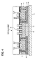
- FIG. 4 is a cross sectional view showing a structure of a substantial portion of a semiconductor device having an element isolation structure according to the third embodiment.
- one of the element formation regions 5 is replaced by a vertical element formation region 16, and a surface electrode 9b is formed over a main side of a wafer substrate 2, and a back surface electrode 15 is formed over a rear side of the wafer substrate 2. Moreover, the back surface electrode 15 is joined to a conductive plate 19 through a conductive joining member 18.
- the other structures of the semiconductor device of the third embodiment are same as those of the second embodiment including a structure that the conductive material 14 arranged inside the trenches 3 and over the rear side of the wafer substrate 2 is fixed to the predetermined potential by the electrode 9a formed over the main side of the wafer substrate 2.
- the back surface electrode 15 deposited over the rear side of the wafer substrate 2 is formed by the same material with the conductive material 14, for example.
- An insulating layer 17 is formed between the back surface electrode 15 and the conductive material 14 for obtaining isolation.
- the conductive material 14 having a predetermined thickness is deposited over the rear side of the wafer substrate 2.
- a portion of the conductive material 14, in which the back surface electrode 15 of the vertical element formation region 16 is formed later, and a region surrounding the portion are removed by etching.
- an insulating material such as silicon oxide is deposited by chemical vapor deposition or the like to form the insulating layer 17.
- a portion of the insulating layer 17, in which the back surface electrode 15 is formed later, is removed by etching, and another conductive material is deposited over the rear side of the wafer substrate 2 to form the back surface electrode 15.
- an insulating layer 4, which has already been formed is also removed.
- the conductive plate 19 is a metal frame supporting a semiconductor chip 20 when the semiconductor ship 20 is packaged, or a copper foil provided over a surface of a mother board when the semiconductor chip 20 is mounted on the mother board.
- the conductive material 14 for electrically shielding the element formation regions 5 is isolated from the layers including the conductive materials such as the joining member 18 and the conductive plate 19, which are formed over an opposite surface to a surface attached to the wafer substrate 2, by the insulating layer 17.
- the conducting material for providing the back surface electrode 15 of the vertical element formation region 16 penetrates the insulating layer 17 so that the back surface electrode 15 is electrically coupled with the layers including the conductive materials, which are formed over the opposite surface. Therefore, the layers including the conductive materials become a part of the back surface electrode 15.
- the conductive material 14 for electrically shielding each of the element formation regions 5 can be formed over the rear side of the wafer substrate 2.
- the conductive plate 19 can be used as a connecting terminal of the back surface electrode 15 by joining the conductive plate 19 to the back surface electrode 15. Moreover, the conductive plate 19 promotes heat release of the element formation regions 5 and 16, and heat release property can be improved.
- Fig. 5 is a cross sectional view showing a structure of a substantial portion of a semiconductor device according to the modification of the third embodiment.
- two conductive materials are laminated with the insulating layer 17 interposed therebetween.
- the conductive material 14 for electrically shielding the element formation regions 5 is a single-layered structure, and a back surface electrode 15a of the vertical element formation region 16 is formed to be thicker than the conductive material 14.
- An insulating layer 17a having a thickness which equals to the difference between the back surface electrode 15a and the conductive material 14 is formed over the conductive material 14.
- the back surface electrode 15a and the insulating layer 17a provide the same surface opposite to the surface attached to the wafer substrate 2.
- the surface configured by the back surface electrode 15a and the insulating layer 17a is joined to the conductive plate 19 through the conductive joining member 18.
- the back surface electrode 15a is isolated from the conductive material 14 by the insulating layer 17a. Since the thickness of the back surface electrode 15a of the vertical element formation region 16 is larger than that of the conductive material 14 for electrically shielding the element formation regions 5, the conductive plate 19 is electrically coupled with only the back surface electrode 15a. Therefore, the conductive plate 19 can be used as the connecting terminal of the back surface electrode 15a.
- potential of the conductive material 14 in the trenches 3 and over the rear side of the wafer substrate 2 are fixed to the predetermined potential by conducting the electrode 9a formed over the main side of the wafer substrate 2 with the conductive material 14 in the trenches 3.
- electrode wirings of each of elements or the like need to be formed over the main side of the wafer substrate 2, a space for providing the electrode 9a is limited.
- radiuses of the conductive material 14 in the trenches 3 are small, and impedance becomes relatively high.
- potential of the conductive material 14 in the trenches 3, which are not coupled with the electrode 9a directly may not be fixed to the predetermined potential stably.
- the conductive material 14 inside the trenches 3 and over the rear side of the wafer substrate 2 is fixed to the predetermined potential by using the conductive plate 19 joined to the rear side of the wafer substrate 2.
- Fig. 6 is a cross sectional view showing a structure of a substantial portion of the semiconductor device having an element isolation structure according to the fourth embodiment.
- the conductive material 14 is formed inside the trenches 3 and over the rear side of the wafer substrate 2.
- the conductive plate 19 is joined to the conductive material 14 formed over the rear side of the wafer substrate 2, which is formed in this manner, through the conductive bonding member 18.
- the ground potential is applied to the conductive plate 19 as the predetermined potential.
- the potential of the conductive material 14 inside the trenches 3 and over the rear side of the wafer substrate 2 through the conductive plate 19 can be fixed to the predetermined potential.
- the potential of the conductive material 14 is fixed by the conductive plate 19, which covers at least portions in which at least the trenches 3 are formed.
- the potential of the conductive material 14 in one of the trenches 3 needs not to be fixed to the predetermined potential via the conductive material 14 having thin radius in another one of the trenches, the electrical connection with low impedance can become possible. Therefore, the potential of the conductive material 14 inside the trenches 3 and over the rear side of the wafer substrate 2 can be kept to the predetermined potential stably.
- Fig. 7 is a cross sectional view showing a structure of a substantial portion of a semiconductor device according to a modification of the fourth embodiment.
- one of the element formation regions 5 is replaced by a vertical element formation region 16.
- the back surface electrode 15 of the vertical element formation region 16 is arranged at the rear side of the wafer substrate 2.
- the conductive plate 19 is divided into an electrode plate 19a coupled with the back surface electrode 15 and a conductive plate 19b coupled with the conductive material 14 in order to applying a predetermined potential to the conductive material 14 in the trenches 3 and over the rear side of the wafer substrate 2 by using the conducive plate 19 over the rear side of the wafer substrate 2.
- An insulating portion 19c is arranged between the electrode plate 19a and the conductive plate 19b, and the electrode plate 19a and the conductive plate 19b are isolated from each other.
- the conductive material 14 in the trenches 3 and over the rear side of the wafer substrate 2 can be fixed, and the back surface electrode 15 of the vertical element formation region 16 can function as the connecting terminal by using the conductive plate 19.
- a plate, in which the electrode plate 19a couples with the conductive plate 19b through the insulating portion 19c, may be prepared in advance, and then the plate is joined to the wafer substrate 2.
- a portion corresponding to the insulating portion 19c may be removed and an insulating material may be inserted to the removed portion.
- voids may remain in vicinity of central axes inside the trenches 3. It takes a long time to fill the trenches 3 completely with the conductive material 14, so that the manufacturing cost increases. Moreover, since the conductive material 14 in the trenches 3 are arranged to prevent the interference of electric potential between the adjacent element formation regions 5, some voids do not disturb the function of the trenches 3.
- the trenches 3 when the trenches 3 is formed in the wafer substrate 2, the trenches 3 may intersect with an impurity diffusion layer 7a in the element formation regions 5. Thereby, the dimensions of the elements, and the cost of the semiconductor chips 20 can be reduced.
- the trenches 3 are formed to surround the element formation regions 5, for example.
- the insulating layer 4 is formed inside the trenches 3 to isolate elements, various arrangements of the element formation regions are possible.
- an element formation region 21 is surrounded by a trench 22, in which an insulating film is formed, and without contacting other element formation regions with a separation region (a field region) 23 interposed therebetween.
- testing for confirming insulating property of the trench 22 can be performed by applying voltage between the field region 23 and the element formation region 21.
- the interference of electric potential of the element formation region 21 can be suppressed by fixing the potential of the field region 23.
- a plurality of element formation regions 24 may be arranged adjacent to each other by being separated with one trench 25.
- the element formation regions 24 can be arranged in the high density, and therefore, more semiconductor chips can be obtained from a wafer substrate 2.
- an element formation region 26 may be isolated by being separated with a plurality of trenches 27 and 28.
- voltage can be shared by the plurality of trenches 27 and 28, and therefore, an element, to which the high voltage is applied, can be arranged in the element formation region 26.
Abstract
Description
- The present invention relates to a semiconductor device having multiple element formation regions and a manufacturing method thereof.
- According to a manufacturing method of the semiconductor device disclosed in
JP-A-2001-144173 USP-6,524,890 andUSP-6,879,029 , a wafer for forming elements is prepared, and trenches each having a predetermined depth from a main side of the wafer are formed firstly. Subsequently, the trenches are filled with an insulating layer, and then, the wafer is thinned by chemical mechanical polishing from a rear side of the wafer, so that the insulating layer is exposed. Thereby, the insulating layer penetrates the wafer and element formation regions can be isolated by the insulating layer. - In the above-mentioned manufacturing method, after the trenches each having the predetermined depth from the main side of the wafer is filled with the insulating layer, the wafer is thinned by chemical mechanical polishing from the rear side of the wafer. Thus, a surface including both a silicon substrate configuring the wafer and the insulating layer made of such as an oxide film needs to be polished. Therefore, stress due to polishing is concentrated at an interface between the silicon substrate and the insulating layer, and cracks may generate in the silicon substrate, for example. In addition, in case that the wafer is thinned by etching not polishing, structural steps may generate over the rear side of the wafer due to the difference of etching rate between the silicon substrate and the insulating layer.
- Moreover, in case that the trenches are not filled sufficiently with the insulating layer, the element formation regions may separate from the wafer by force applied to the element formation regions while the wafer is thinned.
- It is an object of the present disclosure to provide a manufacturing method of a semiconductor device having multiple element formation regions. It is another object of the present disclosure to provide a semiconductor device having multiple element formation regions.
- According to a first aspect of the present disclosure, a method for manufacturing a semiconductor device includes preparing a semiconductor substrate having a main side and a rear side; forming at least one of an active element and a passive element in each of a plurality of element formation regions of the substrate at the main side of the substrate; forming an insulating film over the main side of the substrate; thinning the substrate from the rear side of the substrate; forming a plurality of trenches on the rear side of the substrate in such a manner that each trench reaches the insulating film and surrounds a corresponding one of the plurality of element formation regions after the thinning the substrate; and depositing an insulating material over an inner surface of each trench to form an insulating layer in the trench, so that the plurality of element formation regions are isolated from each other.
- According to the above configuration, a manufacturing method of a semiconductor device having multiple element formation regions, which suppresses generation of cracks and structural steps and separation of element formation regions, and a semiconductor device formed by the manufacturing method can be obtained.
- According to a second aspect of the present disclosure, a semiconductor device includes a semiconductor substrate having a main side and a rear side; a plurality of element formation regions disposed in the substrate; a plurality of trenches, each of which penetrates the substrate, and surrounds a corresponding element formation region; an insulating layer arranged over an inner surface of each trench for isolating the plurality of element formation regions from each other; and at least one of an active element and a passive element arranged in each of the plurality of element formation regions at the main side of the substrate. The insulating layer is arranged over the rear side of the substrate. The insulating layer in each trench is continuously connected to the insulating layer over the rear side.
- According to the above configuration, a manufacturing method of a semiconductor device having multiple element formation regions, which suppresses generation of cracks and structural steps and separation of element formation regions, and a semiconductor device formed by the manufacturing method can be obtained.
- According to a third aspect of the present disclosure, a method for manufacturing a semiconductor device includes preparing a semiconductor substrate having a main side and a rear side; forming at least one of an active element and a passive element in each of a plurality of element formation regions of the substrate at the main side of the substrate; forming an insulating film over the main side of the substrate; forming a conductive body over the insulating film; thinning the substrate from the rear side of the substrate; forming a plurality of trenches on the rear side of the substrate after the thinning the substrate, wherein each trench reaches the insulating film; depositing an insulating material over a sidewall of each trench to form an insulating layer with a void in the trench, so that the plurality of element formation regions are isolated, wherein the void is formed in the insulating layer around a central axis of the trench; removing the insulating film over one of the trench, so that the conductive body is exposed from the rear side of the substrate; and depositing a conductive material in the void in each trench and over the rear side of the substrate. In the depositing the conductive material, the conductive material deposited in each trench is electrically coupled with the conductive body, so that the potential of the conductive material in each trench and over the rear side of the substrate is fixed through the conductive body.
- According to the above configuration, a manufacturing method of a semiconductor device having multiple element formation regions, which suppresses generation of cracks and structural steps and separation of element formation regions, and a semiconductor device formed by the manufacturing method can be obtained.
- According to a fourth aspect of the present disclosure, a semiconductor device includes a semiconductor substrate having a main side and a rear side; a plurality of element formation regions disposed in the substrate; a plurality of trenches, each of which penetrates the substrate, and surrounds a corresponding element formation region; a first insulating layer arranged at least over a sidewall of each trench for isolating the plurality of element formation regions from each other, and arranged over the rear side of the substrate; a first conductive material arranged on the first insulating layer in each trench to fill the trench; at least one of an active element and a passive element arranged in each of the plurality of element formation regions at the main side of the substrate; and a conductive body over the main side of the substrate. The first conductive material is arranged over the rear side of the substrate, and the first conductive material in each trench is continuously connected to the first conductive material over the rear side. In at least one of the trenches, the first conductive material arranged in the at least one of the trenches is electrically coupled with the conductive body, so that the potential of the first conductive material in the at least one of the trenches and over the rear side of the substrate is fixed through the conductive body.
- According to the above configuration, a manufacturing method of a semiconductor device having multiple element formation regions, which suppresses generation of cracks and structural steps and separation of element formation regions, and a semiconductor device formed by the manufacturing method can be obtained.
- The above and other objects, features and advantages of the present invention will become more apparent from the following detailed description made with reference to the accompanying drawings. In the drawings:
-
Fig. 1 is a cross sectional view showing a structure of a substantial portion of a semiconductor device having an element isolation structure according to a first embodiment; -
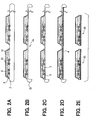
Figs. 2A to 2E are cross sectional views showing a manufacturing method of the semiconductor device according to the first embodiment; -
Fig. 3 is a cross sectional view showing a structure of a substantial portion of a semiconductor device having an element isolation structure according to a second embodiment; -
Fig. 4 is a cross sectional view showing a structure of a substantial portion of a semiconductor device having an element isolation structure according to a third embodiment; -
Fig. 5 is a cross sectional view showing a structure of a substantial portion of a semiconductor device according to a modification of the third embodiment; -
Fig. 6 is a cross sectional view showing a structure of a substantial portion of a semiconductor device having an element isolation structure according to a fourth embodiment; -
Fig. 7 is a cross sectional view showing a structure of a substantial portion of a semiconductor device according to a modification of the fourth embodiment; -
Fig. 8 is an explanation view showing a state that voids remains in a conductive material in trenches; -
Fig. 9 is an explanation view showing a state that trenches intersect with a diffusion layer of an element formation region; and -
Fig. 10 is an explanation view showing an example of arrangement each of element formation regions, which are isolated by trenches. - Hereinafter, embodiments of the present disclosure will be described with reference to the drawings.
Fig. 1 is a cross sectional view showing a structure of a substantial portion of a semiconductor device having an element isolation structure according to a first embodiment. - As shown in
Fig. 1 , a semiconductor device includes a plurality of isolatedelement formation regions 5 over awafer substrate 2 for forming elements, which is made of a silicon substrate. At least one of active elements (a transistor and a diode or the like) and passive elements (a resistor and a capacitor or the like) using the silicon substrate as a semiconductor substrate (a wafer substrate) is formed in each of the plurality ofelement formation regions 5. For example, in case of the transistor,impurity regions 7 are formed by implanting an impurity appropriately, which has opposite conductive type from the silicon substrate, from the main side of the silicon substrate. Theimpurity regions 7 function as a source region and a drain region. By applying voltage to agate electrode 9, a channel is formed between the source region and the drain region, so that current flows therebetween. -
Trenches 3 are formed to surround the plurality ofelement formation regions 5. An insulating material such as silicon oxide is deposited, so that aninsulating layer 4 is formed inside thetrenches 3 and over a rear side of thewafer substrate 2. The plurality ofelement formation regions 5 are isolated each other by theinsulating layer 4. - The
trenches 3 which are filled with the insulatinglayer 4 are formed by etching from the rear side of thewafer substrate 2 as described below. In the etching process, LOCOS (i.e., local oxidation of silicon)films 6 as insulating films formed in a surface portion of thewafer substrate 2 are used as etching stoppers. Thus, each of bottoms of the trenches 3 (each of end portions at the main side of the silicon substrate) contacts the corresponding LOCOS film to terminate. STI (i.e., shallow trench isolation) films may be used as the etching stoppers not LOCOS films. It is possible to use interlayer insulating films such as BPSG (i.e., boro-phospho silicate glass) films as etching stoppers. However, it is preferable to use insulating oxide films such as the above-mentioned LOCOS films and STI films, which have the thickness greater than or equal to sub-microns, in order to improve etching selectivity with the silicon substrate. - A
thermal oxide film 8 is formed over the main side of thewafer substrate 2 after forming the above-mentioned active elements and passive elements. The above-mentionedgate electrode 9 is formed over thethermal oxide film 8. Thegate electrode 9 is made from a conductive body such as polysilicon, tungsten and aluminum. After that, aninterlayer insulating film 10 such as a BPSG film and an NSG film is deposited and formed over thethermal oxide film 8 or thegate electrode 9. Moreover,electrodes 11 andpads 12 of the active elements and the passive elements, which are formed in the plurality ofelement formation regions 5, are formed at portions in which theinterlayer insulating film 10 and thethermal oxide film 8 are removed by etching. - Next, a manufacturing method of the semiconductor device 1 having the above-mentioned structure will be described with reference to
Figs. 2A to 2E . - As shown in
Fig. 2A , thewafer substrate 2 for forming elements, which is made of the silicon substrate, is prepared firstly. Desired elements are formed in each of theelement formation regions 5 from the main side of the silicon substrate. After that, thethermal oxide film 8, thegate electrode 9, the interlayerinsulating films 10,electrodes 11, and apassivation films 13 or the like are formed. According to the manufacturing method of the present embodiment, the semiconductor elements each having the foregoing structure are formed firstly over a plurality of regions of thewafer substrate 2. - Next, as shown in
Fig. 2B , thewafer substrate 2 is thinned by mechanical polishing from the rear side of the wafer substrate 2 (thinning step). In this case, unlike the conventional way that a surface including both a semiconductor substrate and an insulating layer is polished, a surface including only a semiconductor substrate is polished. Thus, the rear side of thewafer substrate 2 can be polished uniformly without generating cracks and structural steps by ordinaly mechanical polishing. Polishing is not limited to the mechanical polishing. Techniques such as chemical mechanical polishing, wet etching and dry etching may be used. - Moreover, in the thinning process, the
wafer substrate 2 is polished until the thickness of thewafer substrate 2 becomes less than or equal to 150 µm, for example. Thereby, it becomes easy to form thetrenches 3 and to deposit the insulating material inside thetrenches 3. However, as the thickness of thewafer substrate 2 becomes thin, the mechanical strength of thewafer substrate 2 decreases. Therefore, cracks may generate in thewafer substrate 2 and handling thewafer substrate 2 may become difficult. - Therefore, it is common that the
wafer substrate 2 is thinned with a supporting base attached to the main side of thewafer substrate 2 for keeping the mechanical strength when thewafer substrate 2 is thinned by polishing from the rear side of thewafer substrate 2. Alternatively, the supporting base may not be attached. In this case, it is preferable that only acentral region 2a surrounded byouter regions 2b is polished, not a whole surface of thewafer substrate 2. Hereby, only thecentral region 2a is thinned, and theouter regions 2b remain without being thinned the thickness thereof. As a result, the decrease of the mechanical strength can be suppressed even if thewafer substrate 2 is thinned. - Moreover, in the process that the supporting base is attached, it becomes difficult to perform the process in the atmosphere greater than or equal to 200 degree Celsius because of the restriction of the retention temperature of an adhesive used for the attachment. However, as described above, the supporting base is not needed when the
outer regions 2b of thewafer substrate 2 remain without being thinned, it becomes possible to perform in the atmosphere greater than or equal to 200 degree Celsius. It is preferable that the thickness of theouter regions 2b are greater than or equal to 250 µm to suppress the decrease of the mechanical strength. - Next, as shown in
Fig. 2C , thetrenches 3 are formed by dry etching from the rear side of thewafer substrate 2, which is thinned. Thetrenches 3 are formed to surround each of theelement formation regions 5. The etching stops by the insulating films when thetrenches 3 reach the insulating films (the LOCOS films 6) in the surface portion of thewafer substrate 2. - In the present embodiment, when the
trenches 3 are formed, thethermal oxide film 8, theinterlayer insulating films 10 have been already formed over thewafer substrate 2. Although thetrenches 3 penetrating thewafer substrate 2 are formed to surround each of the plurality ofelement formation regions 5, each of the regions of thewafer substrate 2 including the plurality ofelement formation regions 5 remains to couple with the semiconductor elements through thethermal oxide film 8 formed over the surface of thewafer substrate 2. Therefore, separation of theelement formation regions 5 can be prevented. - Next, as shown in
Fig. 2D , an insulating material such as silicon oxide is deposited from the rear side of thewafer substrate 2 by direct oxidation, chemical vapor deposition or the like. Thetrenches 3 are filled with the insulating material, so that the insulatinglayer 4 is formed inside thetrenches 3. Therefore, the insulatinglayer 4 is arranged between two adjacentelement formation regions 5 in thewafer substrate 2, and the adjacentelement formation regions 5 are isolated. Moreover, the insulating material continued from the inside thetrenches 3 is deposited also over the rear side of thewafer substrate 2, so that the insulatinglayer 4 is formed. Thereby, protection of the rear side of thewafer substrate 2 and the insulation property can be ensured. - In the present embodiment, as described above, since each of the regions of the
wafer substrate 2 can remain to couple with the semiconductor elements by thethermal oxide film 8 or the like formed over the main side of thewafer substrate 2, being coupling with each of the regions of thewafer substrate 2 by filling thetrenches 3 with the insulatinglayer 4 is not always needed. For example, the insulating material is deposited over inner surfaces of thetrenches 3, and voids may remain in vicinity of central axes inside thetrenches 3. - Finally, as shown in
Fig. 2E , thewafer substrate 2 is divided into a plurality ofchips 20 by die cutting (the separation process). In the separation process, theouter regions 2b remaining without being thinned are separated from the plurality ofchips 20. Asemiconductor chip 20 having an element isolation structure according to the present embodiment is completed through the above-mentioned steps. - Next, a second embodiment of the present disclosure will be described.
Fig. 3 is a cross sectional view showing a structure of a substantial portion of a semiconductor device having an element isolation structure according to the second embodiment. - The differences between the first embodiment and the second embodiment are that, an insulating material is deposited over surfaces of sidewalls of
trenches 3, voids in vicinity of central axes of the trenches 3a are filled with aconductive material 14 made of metal having relatively low melting point, for example, less than or equal to 1100 degree Celsius (such as copper or aluminum), and theconductive material 14 in a portion of thetrenches 3 is electrically coupled with anelectrode 9a formed over a surface of awafer substrate 2, in a semiconductor device of the second embodiment. However, polysilicon having relatively high melting point may be used as theconductive material 14. The structure of the semiconductor device and the manufacturing method thereof according to the second embodiment are similar to those according to the first embodiment. - The insulating
layer 4 is formed between each of two adjacentelement formation regions 5, and the DC component of the electrical signal generated in each of theelement formation regions 5 can be blocked. However, since the AC component of the electrical signal can not be blocked completely, a malfunction may occur by propagation of the AC component. However, the interference of electric potential by the AC component between the adjacentelement formation regions 5 can be prevented by fixing electric potential of theconductive material 14 in thetrenches 3 surrounding theelement formation regions 5, as shown in the above-mentioned configuration. - It is noted that the structure which can obtain the electrical shield between the isolated element formation regions is disclosed in
JP-A-H04-154147 USP-5,442,223 . Specifically, a plurality of element formation regions are formed over an SOI substrate, and trenches between the element formation regions covered by an oxide film are filled with a polysilicon film. - However, in the element isolation structure like this, a conductive layer has already been formed over lower sides and lateral sides of the element formation regions in the semiconductor element forming steps. Therefore, in order to stand high temperature thermal treatment in the element forming steps, polysilicon or a high melting point metal such as tungsten needs to be used as the conductive layer, and the resistivity of the conductive layer becomes high. Moreover, in the conventional element isolation structure, the SOI substrate is used to arrange the conductive layer over lower sides of the element formation regions. In addition to using the conductive layer having high melting point, the manufacturing cost becomes high.
- On the other hand, in the present embodiment,
trenches 3 can be filled with theconductive material 14 after forming elements in the plurality ofelement formation regions 5. Therefore, metal having relatively low melting point such as aluminum or copper can be used for theconductive material 14. Moreover, theconductive material 14 can surround the plurality ofelement formation regions 5 by just depositing theconductive material 14, so that the manufacturing cost can be decreased. - In order to fill
trenches 3 with theconductive material 14, firstly, voids remain in vicinity of central axes of thetrenches 3 and the insulating material is deposited over surfaces of sidewalls of thetrenches 3, so that the insulatinglayer 4 is formed over inner surfaces of thetrenches 3. At this time, the insulating material is deposited and the insulatinglayer 4 is formed over the rear side of thewafer substrate 2. - Next, in one of the
trenches 3 which is arranged opposite to theelectrode 9a formed over the main side of thewafer substrate 2 through thethermal oxide film 8, in case that an insulating material is deposited over a bottom of the one of thetrenches 3 at the main side of thewafer substrate 2, the insulating material and thethermal oxide film 8 are removed by anisotropic etching such as ion beam etching, so that theelectrode 9a is exposed at the bottom of the one of thetrenches 3. And then, voids located in vicinity of central axes of thetrenches 3 including the one of thetrenches 3, in which theelectrode 9a is exposed, are filled with theconductive material 14, and theconductive material 14 is deposited over the rear side of thewafer substrate 2. Thereby, theelectrode 9a over the main side of thewafer substrate 2 can be electrically coupled with theconductive material 14 over the rear side of thewafer substrate 2 through theconductive material 14 inside the one of thetrenches 3. Thereby, theconductive material 14 which is terminated in other trenches oftrenches 3 except the one of thetrenches 3 can also be electrically coupled with theelectrode 9a over the main side of thewafer substrate 2. - In this structure, when applying a predetermined potential to the
electrode 9a over the main side of thewafer substrate 2, theconductive material 14 arranged inside thetrenches 3 and over the rear side of thewafer substrate 2, which is electrically coupled with theelectrode 9a, is fixed to the predetermined potential. Therefore, the interference of electric potential by the AC component between the adjacentelement formation regions 5 can be prevented. It is preferred that the predetermined potential is fixed to the ground potential. Thereby, the electric power consumption can be reduced and the interference of electric potential between the adjacent element formation regions can be prevented. - Next, a third embodiment of the present disclosure will be described.
Fig. 4 is a cross sectional view showing a structure of a substantial portion of a semiconductor device having an element isolation structure according to the third embodiment. - In the present embodiment, one of the
element formation regions 5 is replaced by a verticalelement formation region 16, and asurface electrode 9b is formed over a main side of awafer substrate 2, and aback surface electrode 15 is formed over a rear side of thewafer substrate 2. Moreover, theback surface electrode 15 is joined to aconductive plate 19 through a conductive joiningmember 18. Although not shown in the drawings, the other structures of the semiconductor device of the third embodiment are same as those of the second embodiment including a structure that theconductive material 14 arranged inside thetrenches 3 and over the rear side of thewafer substrate 2 is fixed to the predetermined potential by theelectrode 9a formed over the main side of thewafer substrate 2. - The
back surface electrode 15 deposited over the rear side of thewafer substrate 2 is formed by the same material with theconductive material 14, for example. An insulatinglayer 17 is formed between theback surface electrode 15 and theconductive material 14 for obtaining isolation. In order to obtain the structure having the back surface electrode, firstly, theconductive material 14 having a predetermined thickness is deposited over the rear side of thewafer substrate 2. After that, a portion of theconductive material 14, in which theback surface electrode 15 of the verticalelement formation region 16 is formed later, and a region surrounding the portion are removed by etching. Next, an insulating material such as silicon oxide is deposited by chemical vapor deposition or the like to form the insulatinglayer 17. And then, a portion of the insulatinglayer 17, in which theback surface electrode 15 is formed later, is removed by etching, and another conductive material is deposited over the rear side of thewafer substrate 2 to form theback surface electrode 15. When the portion of the insulatinglayer 17, in which theback surface electrode 15 is formed later, is removed, an insulatinglayer 4, which has already been formed, is also removed. - After that, the
back surface electrode 15 is joined to theconductive plate 19 with the joiningmember 18 made of such as solder, silver paste or metallic nanoparticle, for example. Theconductive plate 19 is a metal frame supporting asemiconductor chip 20 when thesemiconductor ship 20 is packaged, or a copper foil provided over a surface of a mother board when thesemiconductor chip 20 is mounted on the mother board. - That is, in the semiconductor device of the third embodiment, two conductive materials are laminated over the rear side of the
wafer substrate 2 through the insulatinglayer 17, theconductive material 14 for electrically shielding theelement formation regions 5 is isolated from the layers including the conductive materials such as the joiningmember 18 and theconductive plate 19, which are formed over an opposite surface to a surface attached to thewafer substrate 2, by the insulatinglayer 17. On the other hand, the conducting material for providing theback surface electrode 15 of the verticalelement formation region 16 penetrates the insulatinglayer 17 so that theback surface electrode 15 is electrically coupled with the layers including the conductive materials, which are formed over the opposite surface. Therefore, the layers including the conductive materials become a part of theback surface electrode 15. - According to the semiconductor device of the third embodiment configured as described above, even if the
back surface electrode 15 of the verticalelement formation region 16 is formed over the rear side of thewafer substrate 2, with respect to theelement formation regions 5 other than the verticalelement formation region 16, theconductive material 14 for electrically shielding each of theelement formation regions 5 can be formed over the rear side of thewafer substrate 2. Theconductive plate 19 can be used as a connecting terminal of theback surface electrode 15 by joining theconductive plate 19 to theback surface electrode 15. Moreover, theconductive plate 19 promotes heat release of theelement formation regions - Next, a modification of the third embodiment will be described.
Fig. 5 is a cross sectional view showing a structure of a substantial portion of a semiconductor device according to the modification of the third embodiment. In the above-mentioned third embodiment, two conductive materials are laminated with the insulatinglayer 17 interposed therebetween. On the other hand, in the modification shown inFig. 5 , theconductive material 14 for electrically shielding theelement formation regions 5 is a single-layered structure, and aback surface electrode 15a of the verticalelement formation region 16 is formed to be thicker than theconductive material 14. An insulatinglayer 17a having a thickness which equals to the difference between theback surface electrode 15a and theconductive material 14 is formed over theconductive material 14. Therefore, theback surface electrode 15a and the insulatinglayer 17a provide the same surface opposite to the surface attached to thewafer substrate 2. The surface configured by theback surface electrode 15a and the insulatinglayer 17a is joined to theconductive plate 19 through the conductive joiningmember 18. - In this structure, the
back surface electrode 15a is isolated from theconductive material 14 by the insulatinglayer 17a. Since the thickness of theback surface electrode 15a of the verticalelement formation region 16 is larger than that of theconductive material 14 for electrically shielding theelement formation regions 5, theconductive plate 19 is electrically coupled with only theback surface electrode 15a. Therefore, theconductive plate 19 can be used as the connecting terminal of theback surface electrode 15a. - Next, a fourth embodiment of the present disclosure will be described. In the above-mentioned second and third embodiments, potential of the
conductive material 14 in thetrenches 3 and over the rear side of thewafer substrate 2 are fixed to the predetermined potential by conducting theelectrode 9a formed over the main side of thewafer substrate 2 with theconductive material 14 in thetrenches 3. However, since electrode wirings of each of elements or the like need to be formed over the main side of thewafer substrate 2, a space for providing theelectrode 9a is limited. Thus, radiuses of theconductive material 14 in thetrenches 3 are small, and impedance becomes relatively high. Particularly, potential of theconductive material 14 in thetrenches 3, which are not coupled with theelectrode 9a directly, may not be fixed to the predetermined potential stably. - In a semiconductor device of the present embodiment, the
conductive material 14 inside thetrenches 3 and over the rear side of thewafer substrate 2 is fixed to the predetermined potential by using theconductive plate 19 joined to the rear side of thewafer substrate 2. -
Fig. 6 is a cross sectional view showing a structure of a substantial portion of the semiconductor device having an element isolation structure according to the fourth embodiment. As shown inFig. 6 , theconductive material 14 is formed inside thetrenches 3 and over the rear side of thewafer substrate 2. In the present embodiment, theconductive plate 19 is joined to theconductive material 14 formed over the rear side of thewafer substrate 2, which is formed in this manner, through theconductive bonding member 18. The ground potential is applied to theconductive plate 19 as the predetermined potential. Thereby, the potential of theconductive material 14 inside thetrenches 3 and over the rear side of thewafer substrate 2 through theconductive plate 19 can be fixed to the predetermined potential. - Particularly, in the present embodiment, the potential of the
conductive material 14 is fixed by theconductive plate 19, which covers at least portions in which at least thetrenches 3 are formed. In other words, since the potential of theconductive material 14 in one of thetrenches 3 needs not to be fixed to the predetermined potential via theconductive material 14 having thin radius in another one of the trenches, the electrical connection with low impedance can become possible. Therefore, the potential of theconductive material 14 inside thetrenches 3 and over the rear side of thewafer substrate 2 can be kept to the predetermined potential stably. - Next, a modification of the fourth embodiment will be described.
Fig. 7 is a cross sectional view showing a structure of a substantial portion of a semiconductor device according to a modification of the fourth embodiment. In the modification shown inFig. 7 , one of theelement formation regions 5 is replaced by a verticalelement formation region 16. Theback surface electrode 15 of the verticalelement formation region 16 is arranged at the rear side of thewafer substrate 2. Theconductive plate 19 is divided into anelectrode plate 19a coupled with theback surface electrode 15 and aconductive plate 19b coupled with theconductive material 14 in order to applying a predetermined potential to theconductive material 14 in thetrenches 3 and over the rear side of thewafer substrate 2 by using theconducive plate 19 over the rear side of thewafer substrate 2. An insulatingportion 19c is arranged between theelectrode plate 19a and theconductive plate 19b, and theelectrode plate 19a and theconductive plate 19b are isolated from each other. - In this configuration, the
conductive material 14 in thetrenches 3 and over the rear side of thewafer substrate 2 can be fixed, and theback surface electrode 15 of the verticalelement formation region 16 can function as the connecting terminal by using theconductive plate 19. - As the
conductive plate 19, a plate, in which theelectrode plate 19a couples with theconductive plate 19b through the insulatingportion 19c, may be prepared in advance, and then the plate is joined to thewafer substrate 2. Alternatively, after theconductive plate 19 is joined to thewafer substrate 2, a portion corresponding to the insulatingportion 19c may be removed and an insulating material may be inserted to the removed portion. - Although the preferable embodiments are described, the present invention does not limit to the above-mentioned embodiments, and various modifications may be made without departing from the scope of the invention.
- For example, as shown in
Fig. 8 , after theconductive material 14 is deposited in thetrenches 3, voids may remain in vicinity of central axes inside thetrenches 3. It takes a long time to fill thetrenches 3 completely with theconductive material 14, so that the manufacturing cost increases. Moreover, since theconductive material 14 in thetrenches 3 are arranged to prevent the interference of electric potential between the adjacentelement formation regions 5, some voids do not disturb the function of thetrenches 3. - Moreover, as shown in
Fig. 9 , when thetrenches 3 is formed in thewafer substrate 2, thetrenches 3 may intersect with animpurity diffusion layer 7a in theelement formation regions 5. Thereby, the dimensions of the elements, and the cost of the semiconductor chips 20 can be reduced. - In addition, the
trenches 3 are formed to surround theelement formation regions 5, for example. In case that the insulatinglayer 4 is formed inside thetrenches 3 to isolate elements, various arrangements of the element formation regions are possible. - For example, in
Fig. 10 , anelement formation region 21 is surrounded by atrench 22, in which an insulating film is formed, and without contacting other element formation regions with a separation region (a field region) 23 interposed therebetween. In this case, testing for confirming insulating property of thetrench 22 can be performed by applying voltage between thefield region 23 and theelement formation region 21. Moreover, the interference of electric potential of theelement formation region 21 can be suppressed by fixing the potential of thefield region 23. - Moreover, a plurality of
element formation regions 24 may be arranged adjacent to each other by being separated with onetrench 25. In this case, theelement formation regions 24 can be arranged in the high density, and therefore, more semiconductor chips can be obtained from awafer substrate 2. - In addition, an
element formation region 26 may be isolated by being separated with a plurality oftrenches trenches element formation region 26. - While the invention has been described with reference to preferred embodiments thereof, it is to be understood that the invention is not limited to the preferred embodiments and constructions. The invention is intended to cover various modification and equivalent arrangements. In addition, while the various combinations and configurations, which are preferred, other combinations and configurations, including more, less or only a single element, are also within the spirit and scope of the invention.
Claims (22)
- A method for manufacturing a semiconductor device (1) comprising:preparing a semiconductor substrate (2) having a main side and a rear side;forming at least one of an active element and a passive element in each of a plurality of element formation regions (5) of the substrate (2) at the main side of the substrate (2);forming an insulating film (6, 8) over the main side of the substrate (2);thinning the substrate (2) from the rear side of the substrate (2);forming a plurality of trenches (3) on the rear side of the substrate (2) in such a manner that each trench (3) reaches the insulating film (6, 8) and surrounds a corresponding one of the plurality of element formation regions (5) after the thinning the substrate (2); anddepositing an insulating material over an inner surface of each trench (3) to form an insulating layer (4) in the trench (3), so that the plurality of element formation regions (5) are isolated from each other.
- The method for manufacturing the semiconductor device (1) according to claim 1,
wherein a void is formed in the insulating material of each trench (3) around a central axis of the trench (3) in the depositing the insulating material. - The method for manufacturing the semiconductor device (1) according to claim 1,
wherein, in the depositing the insulating material, the insulating material is formed over the rear side of the substrate (2). - The method for manufacturing the semiconductor device (1) according to claim 1,
wherein the insulating film (6, 8) includes at least one of a LOCOS film (6) and an STI film (6), and
wherein the plurality of trenches (3) are formed by etching the substrate (2) with the at least one of the LOCOS film (6) and the STI film (6) as a stopper layer. - The method for manufacturing the semiconductor device (1) according to claim 1,
wherein the substrate (2) is thinned until a thickness of the substrate (2) becomes less than or equal to 150 µm in the thinning the substrate (2). - A semiconductor device (1) comprising:a semiconductor substrate (2) having a main side and a rear side;a plurality of element formation regions (5) disposed in the substrate (2);a plurality of trenches (3), each of which penetrates the substrate (2), and surrounds a corresponding element formation region (5);an insulating layer (4) arranged over an inner surface of each trench (3) for isolating the plurality of element formation regions (5) from each other; andat least one of an active element and a passive element arranged in each of the plurality of element formation regions (5) at the main side of the substrate (2),wherein the insulating layer (4) is further arranged over the rear side of the substrate (2), and
wherein the insulating layer (4) in each trench (3) is continuously connected to the insulating layer (4) over the rear side. - The semiconductor device (1) according to claim 6,
wherein the insulating layer (4) in each trench (3) includes a void around a central axis of the trench (3). - The semiconductor device (1) according to claim 6,
wherein a thickness of the substrate (2) is less than or equal to 150 µm. - A method for manufacturing a semiconductor device (1) comprising:preparing a semiconductor substrate (2) having a main side and a rear side;forming at least one of an active element and a passive element in each of a plurality of element formation regions (5) of the substrate (2) at the main side of the substrate (2);forming an insulating film (6, 8) over the main side of the substrate (2);thinning the substrate (2) from the rear side of the substrate (2);forming a plurality of trenches (3) on the rear side of the substrate (2) after the thinning the substrate (2), wherein each trench (3) reaches the insulating film (6, 8);depositing a first insulating material over a sidewall of each trench (3) and over the rear side of the substrate to form a first insulating layer (4) with a void in the trench (3), so that the plurality of element formation regions (5) are isolated, wherein the void is formed in the first insulating layer (4) around a central axis of the trench (3); anddepositing a first conductive material (14) in the void in each trench (3) and over the rear side of the substrate (2).
- The method for manufacturing the semiconductor device (1) according to claim 9, further comprising:forming a conductive body (9a) over the insulating film (8); andremoving a part of the insulating film (8) over one of the trench (3) from the rear side before the depositing a first conductive material, so that the conductive body (9a) is exposed from the rear side of the substrate (2),wherein, in the depositing the first conductive material (14), the first conductive material (14) deposited in each trench (3) is electrically coupled with the conductive body (9a), so that the potential of the first conductive material (14) in each trench (3) and over the rear side of the substrate (2) is fixed through the conductive body (9a).
- The method for manufacturing the semiconductor device (1) according to claim 9,
wherein the element formation regions (5) includes a vertical element formation region having a back surface electrode over the rear side of the substrate (2),
wherein, in the depositing the first conductive material (14), a second insulating layer (17, 17a) is formed over the first conductive material (14),
wherein, in the depositing the first conductive material (14), a second conductive material (15, 15a) for providing the back surface electrode of the vertical element formation region is deposited over the rear side of the substrate (2), and
wherein the second insulating layer (17, 17a) is disposed between the first conductive material (14) and the second conductive material (15, 15a). - The method for manufacturing the semiconductor device (1) according to claim 9, further comprising:bonding a conductive plate (19) to the first conductive material (14),wherein the potential of the first conductive material (14) in each trench (3) and over the rear side of the substrate (2) is fixed through the conductive plate (19),
wherein the element formation regions (5) includes a vertical element formation region having a back surface electrode over the rear side of the substrate (2), and a part of the first conductive material (14) disposed in the vertical element formation region provides the back surface electrode,
wherein, a third insulating material (19c) is inserted between a first region (19b) and a second region (19a) in the conductive plate (19), and the conductive plate (19) is a divided plate which is electrically divided by the third insulating material (19c),
wherein the first region (19b) is bonded to the first conductive material (14), and
wherein the second region (19a) is bonded to the back surface electrode. - A semiconductor device (1) comprising:a semiconductor substrate (2) having a main side and a rear side;a plurality of element formation regions (5) disposed in the substrate (2);a plurality of trenches (3), each of which penetrates the substrate (2), and surrounds a corresponding element formation region (5);a first insulating layer (4) arranged over a sidewall of each trench (3) for isolating the plurality of element formation regions (5) from each other, and arranged over the rear side of the substrate (2);a first conductive material (14) arranged on the first insulating layer (4) in each trench (3) to fill the trench (3); andat least one of an active element and a passive element arranged in each of the plurality of element formation regions (5) at the main side of the substrate (2),wherein the first conductive material (14) is further arranged over the rear side of the substrate (2), and the first conductive material (14) in each trench (3) is continuously connected to the first conductive material (14) over the rear side.
- The semiconductor device (1) according to claim 13, further comprising:a conductive body (9a) over the main side of the substrate (2),wherein, in at least one of the trenches (3), the first conductive material (14) arranged in the at least one of the trenches (3) is electrically coupled with the conductive body (9a), so that the potential of the first conductive material in the at least one of the trenches (3) and over the rear side of the substrate (2) is fixed through the conductive body (9a).
- The semiconductor device (1) according to claim 13, further comprising:a second conductive material (15, 15a) over the rear side of the substrate (2),
wherein the element formation regions (5) includes a vertical element formation region having a back surface electrode over the rear side of the substrate (2), and the second conductive material (15, 15a) provides the back surface electrode,
wherein the first conductive material (14) and the second conductive material (15, 15a) are arranged over the rear side of the substrate (2), and
wherein a second insulating layer (17, 17a) is arranged between the first conductive material (14) and the second conductive material (15, 15a). - The semiconductor device (1) according to claim 15, further comprising:a conductive plate (19) which is bonded to the second conductive material (15, 15a),wherein the second conductive material (15, 15a) is formed to be thicker than the first conductive material (14), and
wherein the conductive plate (19) is electrically coupled with only the second conductive material (15, 15a). - The semiconductor device (1) according to claim 15, further comprising:a conductive plate (19) which is bonded to the second conductive material (15, 15a),wherein the first conductive material (14) and the second conductive material (15, 15a) are laminated with the second insulating layer (17, 17a) interposed therebetween,
wherein the first conductive material (14) is isolated from the conductive plate (19) by the second insulating layer (17, 17a), and
wherein the second conductive material (15, 15a) penetrates the second insulating layer (17, 17a) so that the back surface electrode is electrically coupled with the conductive plate (19) formed over the opposite surface, and
wherein the conductive plate (19) is electrically coupled with only the second conductive material (15, 15a) for providing the back surface electrode of the vertical element formation region. - The semiconductor device (1) according to claim 13, further comprising:a conductive plate (19) which is bonded to the first conductive material (14),wherein the potential of the first conductive material (14) in each trench (3) and over the rear side of the substrate (2) is fixed through the conductive plate (19).
- The semiconductor device (1) according to claim 18,
wherein the element formation regions (5) includes a vertical element formation region having a back surface electrode over the rear side of the substrate (2) and a part of the first conductive material disposed in the vertical element formation region provides the back surface electrode,
wherein a third insulating material (19c) is disposed between a first region (19b) and a second region (19a) of the conductive plate (19), and the conductive plate (19) is a divided plate which is electrically divided by the third insulating material (19c),
wherein the first region (19b) is bonded to the first conductive material (14), and
wherein the second region (19a) is bonded to the back surface electrode. - The semiconductor device (1) according to claim 18,
wherein the fixed potential of the first conductive material (14) in each trench (3) and over the rear side of the substrate (2) is a ground potential. - The semiconductor device (1) according to claim 13,
wherein a melting point of the first conductive material (14) is less than or equal to 1100 degree Celsius. - The semiconductor device (1) according to claim 13,
wherein a void in the first conductive material (14) in each trench (3) is disposed around the central axis of the trench (3).
Applications Claiming Priority (2)
| Application Number | Priority Date | Filing Date | Title |
|---|---|---|---|
| JP2007220240 | 2007-08-27 | ||
| JP2008106014A JP4687742B2 (en) | 2007-08-27 | 2008-04-15 | Manufacturing method of semiconductor device |
Publications (3)
| Publication Number | Publication Date |
|---|---|
| EP2031653A2 true EP2031653A2 (en) | 2009-03-04 |
| EP2031653A3 EP2031653A3 (en) | 2011-02-16 |
| EP2031653B1 EP2031653B1 (en) | 2014-03-05 |
Family
ID=40130775
Family Applications (1)
| Application Number | Title | Priority Date | Filing Date |
|---|---|---|---|
| EP08014382.9A Expired - Fee Related EP2031653B1 (en) | 2007-08-27 | 2008-08-12 | Manufacturing method for a semiconductor device having multiple element formation regions |
Country Status (2)
| Country | Link |
|---|---|
| US (1) | US7833876B2 (en) |
| EP (1) | EP2031653B1 (en) |
Cited By (1)
| Publication number | Priority date | Publication date | Assignee | Title |
|---|---|---|---|---|
| CN103325822A (en) * | 2012-03-19 | 2013-09-25 | 富士通株式会社 | Compound semiconductor device and method for manufacturing the same |
Families Citing this family (7)
| Publication number | Priority date | Publication date | Assignee | Title |
|---|---|---|---|---|
| JP4924685B2 (en) * | 2009-09-23 | 2012-04-25 | 株式会社デンソー | Semiconductor device and manufacturing method thereof |
| US8928127B2 (en) * | 2010-09-24 | 2015-01-06 | Taiwan Semiconductor Manufacturing Company, Ltd. | Noise decoupling structure with through-substrate vias |
| JP2013143532A (en) * | 2012-01-12 | 2013-07-22 | Toshiba Corp | Semiconductor device |
| TWI528525B (en) * | 2013-09-03 | 2016-04-01 | 瑞昱半導體股份有限公司 | Metal trench de-noise structure and method for foming thesame |
| US9754993B2 (en) * | 2015-08-31 | 2017-09-05 | Taiwan Semiconductor Manufacturing Company, Ltd. | Deep trench isolations and methods of forming the same |
| CN107924831B (en) * | 2015-09-24 | 2023-10-10 | 英特尔公司 | Techniques for exposing a backside of an integrated circuit device and related configurations |
| US10573715B2 (en) * | 2015-12-17 | 2020-02-25 | Intel Corporation | Backside isolation for integrated circuit |
Citations (3)
| Publication number | Priority date | Publication date | Assignee | Title |
|---|---|---|---|---|
| JPH04154147A (en) | 1990-10-17 | 1992-05-27 | Nippondenso Co Ltd | Semiconductor device and manufacture thereof |
| JP2001144173A (en) | 1999-11-17 | 2001-05-25 | Denso Corp | Method of manufacturing semiconductor device |
| US6524890B2 (en) | 1999-11-17 | 2003-02-25 | Denso Corporation | Method for manufacturing semiconductor device having element isolation structure |
Family Cites Families (31)
| Publication number | Priority date | Publication date | Assignee | Title |
|---|---|---|---|---|
| US4612408A (en) | 1984-10-22 | 1986-09-16 | Sera Solar Corporation | Electrically isolated semiconductor integrated photodiode circuits and method |
| JPS62130537A (en) | 1985-12-03 | 1987-06-12 | Toshiba Corp | Method of separating elements of integrated circuit |
| EP0316799B1 (en) | 1987-11-13 | 1994-07-27 | Nissan Motor Co., Ltd. | Semiconductor device |
| US5354695A (en) | 1992-04-08 | 1994-10-11 | Leedy Glenn J | Membrane dielectric isolation IC fabrication |
| JP3111500B2 (en) * | 1991-05-09 | 2000-11-20 | 富士電機株式会社 | Manufacturing method of dielectric isolation wafer |
| JPH0770587B2 (en) | 1991-09-05 | 1995-07-31 | 工業技術院長 | Method for manufacturing semiconductor integrated circuit structure |
| JPH07161809A (en) | 1993-12-02 | 1995-06-23 | Hitachi Ltd | Semiconductor integrated circuit device and its manufacture |
| US5841197A (en) * | 1994-11-18 | 1998-11-24 | Adamic, Jr.; Fred W. | Inverted dielectric isolation process |
| US6124179A (en) * | 1996-09-05 | 2000-09-26 | Adamic, Jr.; Fred W. | Inverted dielectric isolation process |
| US5933746A (en) * | 1996-04-23 | 1999-08-03 | Harris Corporation | Process of forming trench isolation device |
| JPH1027767A (en) | 1996-07-11 | 1998-01-27 | Sanyo Electric Co Ltd | Manufacture of semiconductor device |
| DE19716102C2 (en) * | 1997-04-17 | 2003-09-25 | Infineon Technologies Ag | Integrated circuit arrangement with several components and method for their production |
| JPH11195712A (en) * | 1997-11-05 | 1999-07-21 | Denso Corp | Semiconductor device and manufacture thereof |
| DE19800715A1 (en) | 1998-01-12 | 1999-07-15 | Bremicker Auto Elektrik | Semiconductor element consists of a wafer segmented into isolated individual elements |
| DE19806819A1 (en) * | 1998-02-18 | 1999-08-19 | Siemens Ag | Dielectric insulated (DI)semiconductor device |
| FR2782840B1 (en) | 1998-08-25 | 2003-09-05 | Commissariat Energie Atomique | ELECTRONIC CIRCUIT AND METHOD FOR MAKING AN INTEGRATED ELECTRONIC CIRCUIT COMPRISING AT LEAST ONE ELECTRONIC POWER COMPONENT IN A SUBSTRATE PLATE |
| US6369426B2 (en) | 2000-04-27 | 2002-04-09 | Infineon Technologies North America Corp. | Transistor with integrated photodetector for conductivity modulation |
| KR100854077B1 (en) * | 2002-05-28 | 2008-08-25 | 페어차일드코리아반도체 주식회사 | Method of forming a SOI substrate using wafer bonding techniques and method of manufacturing a high voltage complementary bipolar transistor using the SOI substrate |
| DE10300577B4 (en) | 2003-01-10 | 2012-01-26 | Fraunhofer-Gesellschaft zur Förderung der angewandten Forschung e.V. | Semiconductor device with vertical power device comprising a separation trench and method for its preparation |
| JP4271625B2 (en) | 2004-06-30 | 2009-06-03 | 株式会社フジクラ | Semiconductor package and manufacturing method thereof |
| US7492018B2 (en) * | 2004-09-17 | 2009-02-17 | Taiwan Semiconductor Manufacturing Company, Ltd. | Isolating substrate noise by forming semi-insulating regions |
| JP5048230B2 (en) | 2005-03-30 | 2012-10-17 | オンセミコンダクター・トレーディング・リミテッド | Semiconductor device and manufacturing method thereof |
| JP5151012B2 (en) * | 2005-05-30 | 2013-02-27 | 富士電機株式会社 | Manufacturing method of semiconductor device |
| JP2007035729A (en) | 2005-07-22 | 2007-02-08 | Matsushita Electric Ind Co Ltd | Semiconductor integrated circuit device |
| US7531407B2 (en) * | 2006-07-18 | 2009-05-12 | International Business Machines Corporation | Semiconductor integrated circuit devices having high-Q wafer backside inductors and methods of fabricating same |
| US7427803B2 (en) * | 2006-09-22 | 2008-09-23 | Taiwan Semiconductor Manufacturing Company, Ltd. | Electromagnetic shielding using through-silicon vias |
| US8026572B2 (en) | 2006-12-06 | 2011-09-27 | Denso Corporation | Semiconductor device and method for manufacturing same |
| JP2008227116A (en) * | 2007-03-13 | 2008-09-25 | Renesas Technology Corp | Semiconductor device and its manufacturing method |
| US7485965B2 (en) * | 2007-05-25 | 2009-02-03 | International Business Machines Corporation | Through via in ultra high resistivity wafer and related methods |
| US7936052B2 (en) * | 2008-09-30 | 2011-05-03 | Infineon Technologies Ag | On-chip RF shields with backside redistribution lines |
| JP4894910B2 (en) * | 2009-01-15 | 2012-03-14 | 株式会社デンソー | Manufacturing method of semiconductor device, semiconductor device, and multilayer substrate incorporating the semiconductor device |
-
2008
- 2008-08-12 EP EP08014382.9A patent/EP2031653B1/en not_active Expired - Fee Related
- 2008-08-26 US US12/230,209 patent/US7833876B2/en not_active Expired - Fee Related
Patent Citations (5)
| Publication number | Priority date | Publication date | Assignee | Title |
|---|---|---|---|---|
| JPH04154147A (en) | 1990-10-17 | 1992-05-27 | Nippondenso Co Ltd | Semiconductor device and manufacture thereof |
| US5442223A (en) | 1990-10-17 | 1995-08-15 | Nippondenso Co., Ltd. | Semiconductor device with stress relief |
| JP2001144173A (en) | 1999-11-17 | 2001-05-25 | Denso Corp | Method of manufacturing semiconductor device |
| US6524890B2 (en) | 1999-11-17 | 2003-02-25 | Denso Corporation | Method for manufacturing semiconductor device having element isolation structure |
| US6879029B2 (en) | 1999-11-17 | 2005-04-12 | Denso Corporation | Semiconductor device having element isolation structure |
Cited By (2)
| Publication number | Priority date | Publication date | Assignee | Title |
|---|---|---|---|---|
| CN103325822A (en) * | 2012-03-19 | 2013-09-25 | 富士通株式会社 | Compound semiconductor device and method for manufacturing the same |
| CN103325822B (en) * | 2012-03-19 | 2016-03-30 | 创世舫电子日本株式会社 | Compound semiconductor device and manufacture method thereof |
Also Published As
| Publication number | Publication date |
|---|---|
| EP2031653A3 (en) | 2011-02-16 |
| EP2031653B1 (en) | 2014-03-05 |
| US7833876B2 (en) | 2010-11-16 |
| US20090057812A1 (en) | 2009-03-05 |
Similar Documents
| Publication | Publication Date | Title |
|---|---|---|
| US7833876B2 (en) | Semiconductor device having multiple element formation regions and manufacturing method thereof | |
| US8110900B2 (en) | Manufacturing process of semiconductor device and semiconductor device | |
| US8389331B2 (en) | Apparatus for restricting moisture ingress | |
| JP5048230B2 (en) | Semiconductor device and manufacturing method thereof | |
| US8729711B2 (en) | Semiconductor device | |
| US7906363B2 (en) | Method of fabricating semiconductor device having three-dimensional stacked structure | |
| US8487422B2 (en) | Chip stack with conductive column through electrically insulated semiconductor region | |
| US7935571B2 (en) | Through substrate vias for back-side interconnections on very thin semiconductor wafers | |
| US7498636B2 (en) | Semiconductor device and method of manufacturing the same | |
| US20090061659A1 (en) | Through-hole interconnection structure for semiconductor wafer | |
| US20050218497A1 (en) | Through electrode, spacer provided with the through electrode, and method of manufacturing the same | |
| JP2012142533A (en) | Integrated circuit device and method for preparing the same | |
| US9230908B2 (en) | Through-wafer via device and method of manufacturing the same | |
| JP5271562B2 (en) | Semiconductor device and manufacturing method of semiconductor device | |
| US7375397B2 (en) | Semiconductor device having an SOI structure and method for manufacturing the same | |
| JP5287768B2 (en) | Semiconductor device | |
| CN112563241A (en) | Semiconductor device with a plurality of semiconductor chips | |
| US20220293561A1 (en) | Semiconductor device and method of manufacturing the same | |
| KR20010006415A (en) | Integrated circuit with several components and method for the production thereof | |
| EP2648214B1 (en) | Methods of producing a semiconductor device with a through-substrate via | |
| JP3198761B2 (en) | Semiconductor device | |
| CN116646342A (en) | Semiconductor device and method for manufacturing the same |
Legal Events
| Date | Code | Title | Description |
|---|---|---|---|
| PUAI | Public reference made under article 153(3) epc to a published international application that has entered the european phase |
Free format text: ORIGINAL CODE: 0009012 |
|
| AK | Designated contracting states |
Kind code of ref document: A2 Designated state(s): AT BE BG CH CY CZ DE DK EE ES FI FR GB GR HR HU IE IS IT LI LT LU LV MC MT NL NO PL PT RO SE SI SK TR |
|
| AX | Request for extension of the european patent |
Extension state: AL BA MK RS |
|
| RIN1 | Information on inventor provided before grant (corrected) |
Inventor name: KITAMURA, YASUHIRO Inventor name: AKAGI, NOZOMU Inventor name: FUJII, TETSUO |
|
| PUAL | Search report despatched |
Free format text: ORIGINAL CODE: 0009013 |
|
| AK | Designated contracting states |
Kind code of ref document: A3 Designated state(s): AT BE BG CH CY CZ DE DK EE ES FI FR GB GR HR HU IE IS IT LI LT LU LV MC MT NL NO PL PT RO SE SI SK TR |
|
| AX | Request for extension of the european patent |
Extension state: AL BA MK RS |
|
| 17P | Request for examination filed |
Effective date: 20110816 |
|
| AKX | Designation fees paid |
Designated state(s): DE FR |
|
| 17Q | First examination report despatched |
Effective date: 20120419 |
|
| GRAP | Despatch of communication of intention to grant a patent |
Free format text: ORIGINAL CODE: EPIDOSNIGR1 |
|
| RIC1 | Information provided on ipc code assigned before grant |
Ipc: H01L 23/48 20060101ALI20130826BHEP Ipc: H01L 21/762 20060101AFI20130826BHEP |
|
| INTG | Intention to grant announced |
Effective date: 20130917 |
|
| GRAS | Grant fee paid |
Free format text: ORIGINAL CODE: EPIDOSNIGR3 |
|
| GRAA | (expected) grant |
Free format text: ORIGINAL CODE: 0009210 |
|
| AK | Designated contracting states |
Kind code of ref document: B1 Designated state(s): DE FR |
|
| REG | Reference to a national code |
Ref country code: DE Ref legal event code: R096 Ref document number: 602008030547 Country of ref document: DE Effective date: 20140417 |
|
| REG | Reference to a national code |
Ref country code: DE Ref legal event code: R084 Ref document number: 602008030547 Country of ref document: DE |
|
| REG | Reference to a national code |
Ref country code: DE Ref legal event code: R097 Ref document number: 602008030547 Country of ref document: DE |
|
| REG | Reference to a national code |
Ref country code: DE Ref legal event code: R084 Ref document number: 602008030547 Country of ref document: DE Effective date: 20141113 |
|
| PLBE | No opposition filed within time limit |
Free format text: ORIGINAL CODE: 0009261 |
|
| STAA | Information on the status of an ep patent application or granted ep patent |
Free format text: STATUS: NO OPPOSITION FILED WITHIN TIME LIMIT |
|
| 26N | No opposition filed |
Effective date: 20141208 |
|
| REG | Reference to a national code |
Ref country code: DE Ref legal event code: R097 Ref document number: 602008030547 Country of ref document: DE Effective date: 20141208 |
|
| REG | Reference to a national code |
Ref country code: FR Ref legal event code: PLFP Year of fee payment: 8 |
|
| REG | Reference to a national code |
Ref country code: FR Ref legal event code: PLFP Year of fee payment: 9 |
|
| PGFP | Annual fee paid to national office [announced via postgrant information from national office to epo] |
Ref country code: FR Payment date: 20160822 Year of fee payment: 9 |
|
| REG | Reference to a national code |
Ref country code: FR Ref legal event code: ST Effective date: 20180430 |
|
| PG25 | Lapsed in a contracting state [announced via postgrant information from national office to epo] |
Ref country code: FR Free format text: LAPSE BECAUSE OF NON-PAYMENT OF DUE FEES Effective date: 20170831 |
|
| PGFP | Annual fee paid to national office [announced via postgrant information from national office to epo] |
Ref country code: DE Payment date: 20180823 Year of fee payment: 11 |
|
| REG | Reference to a national code |
Ref country code: DE Ref legal event code: R119 Ref document number: 602008030547 Country of ref document: DE |
|
| PG25 | Lapsed in a contracting state [announced via postgrant information from national office to epo] |
Ref country code: DE Free format text: LAPSE BECAUSE OF NON-PAYMENT OF DUE FEES Effective date: 20200303 |