EP2003695A2 - Thin film transistor, method of fabricating the thin film transistor, and display device including the thin film transistor - Google Patents
Thin film transistor, method of fabricating the thin film transistor, and display device including the thin film transistor Download PDFInfo
- Publication number
- EP2003695A2 EP2003695A2 EP08252041A EP08252041A EP2003695A2 EP 2003695 A2 EP2003695 A2 EP 2003695A2 EP 08252041 A EP08252041 A EP 08252041A EP 08252041 A EP08252041 A EP 08252041A EP 2003695 A2 EP2003695 A2 EP 2003695A2
- Authority
- EP
- European Patent Office
- Prior art keywords
- metal
- layer
- semiconductor layer
- crystallization
- channel region
- Prior art date
- Legal status (The legal status is an assumption and is not a legal conclusion. Google has not performed a legal analysis and makes no representation as to the accuracy of the status listed.)
- Withdrawn
Links
- 239000010409 thin film Substances 0.000 title claims abstract description 30
- 238000004519 manufacturing process Methods 0.000 title claims abstract description 15
- 229910052751 metal Inorganic materials 0.000 claims abstract description 351
- 239000002184 metal Substances 0.000 claims abstract description 351
- 239000004065 semiconductor Substances 0.000 claims abstract description 221
- 238000002425 crystallisation Methods 0.000 claims abstract description 172
- 230000008025 crystallization Effects 0.000 claims abstract description 172
- 230000001939 inductive effect Effects 0.000 claims abstract description 147
- 229910021332 silicide Inorganic materials 0.000 claims abstract description 97
- FVBUAEGBCNSCDD-UHFFFAOYSA-N silicide(4-) Chemical compound [Si-4] FVBUAEGBCNSCDD-UHFFFAOYSA-N 0.000 claims abstract description 94
- 239000010410 layer Substances 0.000 claims description 508
- 238000000034 method Methods 0.000 claims description 104
- 229910021417 amorphous silicon Inorganic materials 0.000 claims description 58
- 229910021420 polycrystalline silicon Inorganic materials 0.000 claims description 43
- 239000000758 substrate Substances 0.000 claims description 34
- 238000005247 gettering Methods 0.000 claims description 29
- 238000009792 diffusion process Methods 0.000 claims description 24
- 238000000137 annealing Methods 0.000 claims description 23
- PXHVJJICTQNCMI-UHFFFAOYSA-N Nickel Chemical compound [Ni] PXHVJJICTQNCMI-UHFFFAOYSA-N 0.000 claims description 22
- XUIMIQQOPSSXEZ-UHFFFAOYSA-N Silicon Chemical compound [Si] XUIMIQQOPSSXEZ-UHFFFAOYSA-N 0.000 claims description 10
- 229910052710 silicon Inorganic materials 0.000 claims description 10
- 239000010703 silicon Substances 0.000 claims description 10
- 229910045601 alloy Inorganic materials 0.000 claims description 7
- 239000000956 alloy Substances 0.000 claims description 7
- 239000012044 organic layer Substances 0.000 claims description 7
- 238000000059 patterning Methods 0.000 claims description 7
- 229910052804 chromium Inorganic materials 0.000 claims description 5
- 229910052750 molybdenum Inorganic materials 0.000 claims description 5
- 229910052759 nickel Inorganic materials 0.000 claims description 5
- 229910052719 titanium Inorganic materials 0.000 claims description 4
- 229910052721 tungsten Inorganic materials 0.000 claims description 4
- 229910052684 Cerium Inorganic materials 0.000 claims description 3
- 229910052692 Dysprosium Inorganic materials 0.000 claims description 3
- 229910052689 Holmium Inorganic materials 0.000 claims description 3
- 229910052779 Neodymium Inorganic materials 0.000 claims description 3
- 229910052777 Praseodymium Inorganic materials 0.000 claims description 3
- 229910052735 hafnium Inorganic materials 0.000 claims description 3
- 229910052741 iridium Inorganic materials 0.000 claims description 3
- 229910052746 lanthanum Inorganic materials 0.000 claims description 3
- 229910052748 manganese Inorganic materials 0.000 claims description 3
- 239000000463 material Substances 0.000 claims description 3
- 229910052758 niobium Inorganic materials 0.000 claims description 3
- 229910052762 osmium Inorganic materials 0.000 claims description 3
- 229910052697 platinum Inorganic materials 0.000 claims description 3
- 229910052702 rhenium Inorganic materials 0.000 claims description 3
- 229910052703 rhodium Inorganic materials 0.000 claims description 3
- 229910052707 ruthenium Inorganic materials 0.000 claims description 3
- 229910052706 scandium Inorganic materials 0.000 claims description 3
- 229910052715 tantalum Inorganic materials 0.000 claims description 3
- 229910052720 vanadium Inorganic materials 0.000 claims description 3
- 229910052727 yttrium Inorganic materials 0.000 claims description 3
- 229910052726 zirconium Inorganic materials 0.000 claims description 3
- 229910052718 tin Inorganic materials 0.000 claims description 2
- 230000001419 dependent effect Effects 0.000 claims 2
- 229910004166 TaN Inorganic materials 0.000 claims 1
- ATJFFYVFTNAWJD-UHFFFAOYSA-N Tin Chemical compound [Sn] ATJFFYVFTNAWJD-UHFFFAOYSA-N 0.000 claims 1
- 230000007423 decrease Effects 0.000 description 16
- 229910052581 Si3N4 Inorganic materials 0.000 description 9
- 239000012535 impurity Substances 0.000 description 9
- HQVNEWCFYHHQES-UHFFFAOYSA-N silicon nitride Chemical compound N12[Si]34N5[Si]62N3[Si]51N64 HQVNEWCFYHHQES-UHFFFAOYSA-N 0.000 description 9
- VYPSYNLAJGMNEJ-UHFFFAOYSA-N Silicium dioxide Chemical compound O=[Si]=O VYPSYNLAJGMNEJ-UHFFFAOYSA-N 0.000 description 8
- 229910052814 silicon oxide Inorganic materials 0.000 description 8
- 150000002500 ions Chemical class 0.000 description 7
- 229910052782 aluminium Inorganic materials 0.000 description 6
- 239000011651 chromium Substances 0.000 description 6
- 230000000694 effects Effects 0.000 description 6
- 239000011229 interlayer Substances 0.000 description 6
- 239000002365 multiple layer Substances 0.000 description 6
- 229920002120 photoresistant polymer Polymers 0.000 description 6
- 229910000838 Al alloy Inorganic materials 0.000 description 5
- UBSJOWMHLJZVDJ-UHFFFAOYSA-N aluminum neodymium Chemical compound [Al].[Nd] UBSJOWMHLJZVDJ-UHFFFAOYSA-N 0.000 description 5
- KDLHZDBZIXYQEI-UHFFFAOYSA-N Palladium Chemical compound [Pd] KDLHZDBZIXYQEI-UHFFFAOYSA-N 0.000 description 4
- XAGFODPZIPBFFR-UHFFFAOYSA-N aluminium Chemical compound [Al] XAGFODPZIPBFFR-UHFFFAOYSA-N 0.000 description 4
- 238000005229 chemical vapour deposition Methods 0.000 description 4
- 239000013078 crystal Substances 0.000 description 4
- 238000005240 physical vapour deposition Methods 0.000 description 4
- 239000002356 single layer Substances 0.000 description 4
- 239000010936 titanium Substances 0.000 description 4
- NRTOMJZYCJJWKI-UHFFFAOYSA-N Titanium nitride Chemical compound [Ti]#N NRTOMJZYCJJWKI-UHFFFAOYSA-N 0.000 description 3
- 238000000151 deposition Methods 0.000 description 3
- 239000011521 glass Substances 0.000 description 3
- 239000004973 liquid crystal related substance Substances 0.000 description 3
- 238000000611 regression analysis Methods 0.000 description 3
- VYZAMTAEIAYCRO-UHFFFAOYSA-N Chromium Chemical compound [Cr] VYZAMTAEIAYCRO-UHFFFAOYSA-N 0.000 description 2
- 229910001182 Mo alloy Inorganic materials 0.000 description 2
- ZOKXTWBITQBERF-UHFFFAOYSA-N Molybdenum Chemical compound [Mo] ZOKXTWBITQBERF-UHFFFAOYSA-N 0.000 description 2
- 229910052787 antimony Inorganic materials 0.000 description 2
- UMIVXZPTRXBADB-UHFFFAOYSA-N benzocyclobutene Chemical compound C1=CC=C2CCC2=C1 UMIVXZPTRXBADB-UHFFFAOYSA-N 0.000 description 2
- 229910001423 beryllium ion Inorganic materials 0.000 description 2
- 230000005540 biological transmission Effects 0.000 description 2
- 230000000903 blocking effect Effects 0.000 description 2
- 239000010949 copper Substances 0.000 description 2
- 238000005530 etching Methods 0.000 description 2
- 230000001965 increasing effect Effects 0.000 description 2
- 238000002347 injection Methods 0.000 description 2
- 239000007924 injection Substances 0.000 description 2
- 239000011733 molybdenum Substances 0.000 description 2
- 229910052763 palladium Inorganic materials 0.000 description 2
- 239000004033 plastic Substances 0.000 description 2
- 238000004151 rapid thermal annealing Methods 0.000 description 2
- 229910052709 silver Inorganic materials 0.000 description 2
- NIXOWILDQLNWCW-UHFFFAOYSA-M Acrylate Chemical compound [O-]C(=O)C=C NIXOWILDQLNWCW-UHFFFAOYSA-M 0.000 description 1
- ZOXJGFHDIHLPTG-UHFFFAOYSA-N Boron Chemical compound [B] ZOXJGFHDIHLPTG-UHFFFAOYSA-N 0.000 description 1
- RYGMFSIKBFXOCR-UHFFFAOYSA-N Copper Chemical compound [Cu] RYGMFSIKBFXOCR-UHFFFAOYSA-N 0.000 description 1
- 229910000599 Cr alloy Inorganic materials 0.000 description 1
- 229910000881 Cu alloy Inorganic materials 0.000 description 1
- GYHNNYVSQQEPJS-UHFFFAOYSA-N Gallium Chemical compound [Ga] GYHNNYVSQQEPJS-UHFFFAOYSA-N 0.000 description 1
- UFHFLCQGNIYNRP-UHFFFAOYSA-N Hydrogen Chemical compound [H][H] UFHFLCQGNIYNRP-UHFFFAOYSA-N 0.000 description 1
- OAICVXFJPJFONN-UHFFFAOYSA-N Phosphorus Chemical compound [P] OAICVXFJPJFONN-UHFFFAOYSA-N 0.000 description 1
- 239000004642 Polyimide Substances 0.000 description 1
- RTAQQCXQSZGOHL-UHFFFAOYSA-N Titanium Chemical compound [Ti] RTAQQCXQSZGOHL-UHFFFAOYSA-N 0.000 description 1
- WATWJIUSRGPENY-UHFFFAOYSA-N antimony atom Chemical compound [Sb] WATWJIUSRGPENY-UHFFFAOYSA-N 0.000 description 1
- 229910052785 arsenic Inorganic materials 0.000 description 1
- RQNWIZPPADIBDY-UHFFFAOYSA-N arsenic atom Chemical compound [As] RQNWIZPPADIBDY-UHFFFAOYSA-N 0.000 description 1
- 229910052788 barium Inorganic materials 0.000 description 1
- 230000004888 barrier function Effects 0.000 description 1
- 230000015572 biosynthetic process Effects 0.000 description 1
- 229910052796 boron Inorganic materials 0.000 description 1
- 229910052793 cadmium Inorganic materials 0.000 description 1
- 229910052791 calcium Inorganic materials 0.000 description 1
- 238000006243 chemical reaction Methods 0.000 description 1
- 239000004020 conductor Substances 0.000 description 1
- 229910052802 copper Inorganic materials 0.000 description 1
- 230000003247 decreasing effect Effects 0.000 description 1
- 238000006356 dehydrogenation reaction Methods 0.000 description 1
- 230000005496 eutectics Effects 0.000 description 1
- 229910052733 gallium Inorganic materials 0.000 description 1
- 229910052737 gold Inorganic materials 0.000 description 1
- 239000010931 gold Substances 0.000 description 1
- 230000005525 hole transport Effects 0.000 description 1
- 229910052739 hydrogen Inorganic materials 0.000 description 1
- 239000001257 hydrogen Substances 0.000 description 1
- 229910052738 indium Inorganic materials 0.000 description 1
- APFVFJFRJDLVQX-UHFFFAOYSA-N indium atom Chemical compound [In] APFVFJFRJDLVQX-UHFFFAOYSA-N 0.000 description 1
- AMGQUBHHOARCQH-UHFFFAOYSA-N indium;oxotin Chemical compound [In].[Sn]=O AMGQUBHHOARCQH-UHFFFAOYSA-N 0.000 description 1
- 238000005224 laser annealing Methods 0.000 description 1
- 229910052749 magnesium Inorganic materials 0.000 description 1
- 239000011159 matrix material Substances 0.000 description 1
- MGRWKWACZDFZJT-UHFFFAOYSA-N molybdenum tungsten Chemical compound [Mo].[W] MGRWKWACZDFZJT-UHFFFAOYSA-N 0.000 description 1
- 229910052698 phosphorus Inorganic materials 0.000 description 1
- 239000011574 phosphorus Substances 0.000 description 1
- 229920001721 polyimide Polymers 0.000 description 1
- 238000012887 quadratic function Methods 0.000 description 1
- 239000011347 resin Substances 0.000 description 1
- 229920005989 resin Polymers 0.000 description 1
- 239000010944 silver (metal) Substances 0.000 description 1
- 239000007790 solid phase Substances 0.000 description 1
- 239000010935 stainless steel Substances 0.000 description 1
- 229910001220 stainless steel Inorganic materials 0.000 description 1
- 230000008646 thermal stress Effects 0.000 description 1
- WFKWXMTUELFFGS-UHFFFAOYSA-N tungsten Chemical compound [W] WFKWXMTUELFFGS-UHFFFAOYSA-N 0.000 description 1
- 239000010937 tungsten Substances 0.000 description 1
- YVTHLONGBIQYBO-UHFFFAOYSA-N zinc indium(3+) oxygen(2-) Chemical compound [O--].[Zn++].[In+3] YVTHLONGBIQYBO-UHFFFAOYSA-N 0.000 description 1
- TYHJXGDMRRJCRY-UHFFFAOYSA-N zinc indium(3+) oxygen(2-) tin(4+) Chemical compound [O-2].[Zn+2].[Sn+4].[In+3] TYHJXGDMRRJCRY-UHFFFAOYSA-N 0.000 description 1
Images


Classifications
-
- H—ELECTRICITY
- H01—ELECTRIC ELEMENTS
- H01L—SEMICONDUCTOR DEVICES NOT COVERED BY CLASS H10
- H01L29/00—Semiconductor devices adapted for rectifying, amplifying, oscillating or switching, or capacitors or resistors with at least one potential-jump barrier or surface barrier, e.g. PN junction depletion layer or carrier concentration layer; Details of semiconductor bodies or of electrodes thereof ; Multistep manufacturing processes therefor
- H01L29/66—Types of semiconductor device ; Multistep manufacturing processes therefor
- H01L29/68—Types of semiconductor device ; Multistep manufacturing processes therefor controllable by only the electric current supplied, or only the electric potential applied, to an electrode which does not carry the current to be rectified, amplified or switched
- H01L29/76—Unipolar devices, e.g. field effect transistors
- H01L29/772—Field effect transistors
- H01L29/78—Field effect transistors with field effect produced by an insulated gate
- H01L29/786—Thin film transistors, i.e. transistors with a channel being at least partly a thin film
- H01L29/78606—Thin film transistors, i.e. transistors with a channel being at least partly a thin film with supplementary region or layer in the thin film or in the insulated bulk substrate supporting it for controlling or increasing the safety of the device
- H01L29/78609—Thin film transistors, i.e. transistors with a channel being at least partly a thin film with supplementary region or layer in the thin film or in the insulated bulk substrate supporting it for controlling or increasing the safety of the device for preventing leakage current
-
- H—ELECTRICITY
- H01—ELECTRIC ELEMENTS
- H01L—SEMICONDUCTOR DEVICES NOT COVERED BY CLASS H10
- H01L27/00—Devices consisting of a plurality of semiconductor or other solid-state components formed in or on a common substrate
- H01L27/02—Devices consisting of a plurality of semiconductor or other solid-state components formed in or on a common substrate including semiconductor components specially adapted for rectifying, oscillating, amplifying or switching and having at least one potential-jump barrier or surface barrier; including integrated passive circuit elements with at least one potential-jump barrier or surface barrier
- H01L27/12—Devices consisting of a plurality of semiconductor or other solid-state components formed in or on a common substrate including semiconductor components specially adapted for rectifying, oscillating, amplifying or switching and having at least one potential-jump barrier or surface barrier; including integrated passive circuit elements with at least one potential-jump barrier or surface barrier the substrate being other than a semiconductor body, e.g. an insulating body
-
- H—ELECTRICITY
- H01—ELECTRIC ELEMENTS
- H01L—SEMICONDUCTOR DEVICES NOT COVERED BY CLASS H10
- H01L21/00—Processes or apparatus adapted for the manufacture or treatment of semiconductor or solid state devices or of parts thereof
- H01L21/02—Manufacture or treatment of semiconductor devices or of parts thereof
- H01L21/02104—Forming layers
- H01L21/02365—Forming inorganic semiconducting materials on a substrate
- H01L21/02436—Intermediate layers between substrates and deposited layers
- H01L21/02439—Materials
- H01L21/02488—Insulating materials
-
- H—ELECTRICITY
- H01—ELECTRIC ELEMENTS
- H01L—SEMICONDUCTOR DEVICES NOT COVERED BY CLASS H10
- H01L21/00—Processes or apparatus adapted for the manufacture or treatment of semiconductor or solid state devices or of parts thereof
- H01L21/02—Manufacture or treatment of semiconductor devices or of parts thereof
- H01L21/02104—Forming layers
- H01L21/02365—Forming inorganic semiconducting materials on a substrate
- H01L21/02518—Deposited layers
- H01L21/02521—Materials
- H01L21/02524—Group 14 semiconducting materials
- H01L21/02532—Silicon, silicon germanium, germanium
-
- H—ELECTRICITY
- H01—ELECTRIC ELEMENTS
- H01L—SEMICONDUCTOR DEVICES NOT COVERED BY CLASS H10
- H01L21/00—Processes or apparatus adapted for the manufacture or treatment of semiconductor or solid state devices or of parts thereof
- H01L21/02—Manufacture or treatment of semiconductor devices or of parts thereof
- H01L21/02104—Forming layers
- H01L21/02365—Forming inorganic semiconducting materials on a substrate
- H01L21/02656—Special treatments
- H01L21/02664—Aftertreatments
- H01L21/02667—Crystallisation or recrystallisation of non-monocrystalline semiconductor materials, e.g. regrowth
- H01L21/02672—Crystallisation or recrystallisation of non-monocrystalline semiconductor materials, e.g. regrowth using crystallisation enhancing elements
-
- H—ELECTRICITY
- H01—ELECTRIC ELEMENTS
- H01L—SEMICONDUCTOR DEVICES NOT COVERED BY CLASS H10
- H01L27/00—Devices consisting of a plurality of semiconductor or other solid-state components formed in or on a common substrate
- H01L27/02—Devices consisting of a plurality of semiconductor or other solid-state components formed in or on a common substrate including semiconductor components specially adapted for rectifying, oscillating, amplifying or switching and having at least one potential-jump barrier or surface barrier; including integrated passive circuit elements with at least one potential-jump barrier or surface barrier
- H01L27/12—Devices consisting of a plurality of semiconductor or other solid-state components formed in or on a common substrate including semiconductor components specially adapted for rectifying, oscillating, amplifying or switching and having at least one potential-jump barrier or surface barrier; including integrated passive circuit elements with at least one potential-jump barrier or surface barrier the substrate being other than a semiconductor body, e.g. an insulating body
- H01L27/1214—Devices consisting of a plurality of semiconductor or other solid-state components formed in or on a common substrate including semiconductor components specially adapted for rectifying, oscillating, amplifying or switching and having at least one potential-jump barrier or surface barrier; including integrated passive circuit elements with at least one potential-jump barrier or surface barrier the substrate being other than a semiconductor body, e.g. an insulating body comprising a plurality of TFTs formed on a non-semiconducting substrate, e.g. driving circuits for AMLCDs
- H01L27/1259—Multistep manufacturing methods
- H01L27/127—Multistep manufacturing methods with a particular formation, treatment or patterning of the active layer specially adapted to the circuit arrangement
- H01L27/1274—Multistep manufacturing methods with a particular formation, treatment or patterning of the active layer specially adapted to the circuit arrangement using crystallisation of amorphous semiconductor or recrystallisation of crystalline semiconductor
- H01L27/1277—Multistep manufacturing methods with a particular formation, treatment or patterning of the active layer specially adapted to the circuit arrangement using crystallisation of amorphous semiconductor or recrystallisation of crystalline semiconductor using a crystallisation promoting species, e.g. local introduction of Ni catalyst
-
- H—ELECTRICITY
- H01—ELECTRIC ELEMENTS
- H01L—SEMICONDUCTOR DEVICES NOT COVERED BY CLASS H10
- H01L29/00—Semiconductor devices adapted for rectifying, amplifying, oscillating or switching, or capacitors or resistors with at least one potential-jump barrier or surface barrier, e.g. PN junction depletion layer or carrier concentration layer; Details of semiconductor bodies or of electrodes thereof ; Multistep manufacturing processes therefor
- H01L29/66—Types of semiconductor device ; Multistep manufacturing processes therefor
- H01L29/68—Types of semiconductor device ; Multistep manufacturing processes therefor controllable by only the electric current supplied, or only the electric potential applied, to an electrode which does not carry the current to be rectified, amplified or switched
- H01L29/76—Unipolar devices, e.g. field effect transistors
- H01L29/772—Field effect transistors
- H01L29/78—Field effect transistors with field effect produced by an insulated gate
- H01L29/786—Thin film transistors, i.e. transistors with a channel being at least partly a thin film
- H01L29/78696—Thin film transistors, i.e. transistors with a channel being at least partly a thin film characterised by the structure of the channel, e.g. multichannel, transverse or longitudinal shape, length or width, doping structure, or the overlap or alignment between the channel and the gate, the source or the drain, or the contacting structure of the channel
Landscapes
- Engineering & Computer Science (AREA)
- Power Engineering (AREA)
- Microelectronics & Electronic Packaging (AREA)
- Condensed Matter Physics & Semiconductors (AREA)
- General Physics & Mathematics (AREA)
- Computer Hardware Design (AREA)
- Physics & Mathematics (AREA)
- Manufacturing & Machinery (AREA)
- Chemical & Material Sciences (AREA)
- Crystallography & Structural Chemistry (AREA)
- Chemical Kinetics & Catalysis (AREA)
- Ceramic Engineering (AREA)
- Thin Film Transistor (AREA)
- Recrystallisation Techniques (AREA)
- Electroluminescent Light Sources (AREA)
- Electrodes Of Semiconductors (AREA)
Abstract
Description
- Aspects of the present invention relate to a thin film transistor (TFT), a method of fabricating the TFT, and a display device including the TFT, and more particularly, to a TFT in which a length L(µm) of a channel region of a semiconductor layer and a leakage current loff/W(A/mm) per 1mm of a width W of the channel region of the semiconductor layer satisfies a function loff/W=(3.4x10-15)L2+(2.4 x10-12)L+c, wherein "c" is a constant ranging from 2.5x10⁻¹³ to 6.8x10⁻¹³, a method of fabricating the TFT, and a display device including the TFT.
- In general, thin film transistors (TFTs) are used as active devices of active matrix liquid crystal displays (AMLCDs) and switching devices and driving devices of organic light emitting diode (OLED) display devices. It is necessary to control the characteristics of a TFT according to the characteristics of each device. In this case, a leakage current significantly affects the characteristics of the TFT.
- Conventionally, in a TFT using a polycrystalline silicon (poly-Si) layer, crystallized using a metal-free crystallization technique, as a semiconductor layer, a leakage current is proportional to the width of a channel region and inversely proportional to the length of the channel region. However, even if the length of the channel region is increased in order to reduce the leakage current, it is difficult to produce the intended effect. Furthermore, in a display device, as the length of a channel region increases, the size of the display device also increases and an aperture ratio decreases. Therefore, there is a specific technical limit to increase the length of the channel region.
- Meanwhile, a vast amount of research is being conducted on a crystallization technique using a crystallization-inducing metal, for example a metal induced crystallization (MIC) technique, a metal induced lateral crystallization(MILC) technique and a super grain silicon(SGS) technique, because the techniques may crystallize an amorphous silicon (a-Si) layer at a lower temperature in a shorter amount of time than a solid-phase crystallization (SPC) technique or an excimer laser annealing (ELA) technique. However, in a TFT using a poly-Si layer crystallized using the crystallization-inducing metal as a semiconductor layer, a leakage current of the TFT varies irrespective of the length or width of a channel region unlike in typical TFTs.
- Therefore, in the TFT using the poly-Si layer crystallized using the crystallization-inducing metal as the semiconductor layer, it is impossible to predict a leakage current relative to the size of the channel region of the semiconductor layer. Also, it is difficult to determine the size of the channel region in order to obtain a desired leakage current.
- Aspects of the present invention provide a thin film transistor (TFT) using a semiconductor layer crystallized using a crystallization-inducing metal, a method of fabricating the TFT, and a display device including the TFT. In the TFT using the semiconductor layer crystallized using the crystallization-inducing metal, a leakage current may be reduced by eliminating a crystallization-inducing metal from a channel region of the semiconductor layer. Also, a leakage current may be predicted according to the width and length of the channel region of the semiconductor layer. Conversely, the width and length of the channel region of the semiconductor layer may be determined considering a leakage current to be controlled.
- According to an aspect of the present invention, a TFT includes: a substrate; a semiconductor layer disposed on the substrate, the semiconductor layer including a channel region and source and drain regions, and the semiconductor layer being crystallized using a crystallization-inducing metal; a gate electrode disposed to correspond to a predetermined region of the semiconductor layer; a gate insulating layer disposed between the gate electrode and the semiconductor layer to insulate the semiconductor layer from the gate electrode; and source and drain electrodes respectively electrically connected to the source and drain regions of the semiconductor layer, a metal other than the crystallization-inducing metal or a silicide of a metal different from the crystallization-inducing metal disposed at a predetermined depth from a surface of the semiconductor layer in a region spaced apart from the channel region in the semiconductor layer, and a length and width of the channel region of the semiconductor layer and a leakage current of the semiconductor layer satisfy the following equation: loff/W=(3.4x10-15)L2+(2.4x10-12)L+c, wherein loff (A) is the leakage current of the semiconductor layer, W (mm) is the width of the channel region, L(µm) is the length of the channel region, and "c" is a constant ranging from 2.5x10⁻¹³ to 6.8x10⁻¹³.
- According to another aspect of the present invention, a method of fabricating a TFT includes: providing a substrate; forming an amorphous silicon (a-Si) layer on the substrate; crystallizing the a-Si layer into a polycrystalline silicon (poly-Si) layer using a crystallization-inducing metal; determining a length and width of a channel region of a semiconductor layer according to a leakage current to be controlled using the following equation: loff/W=(3.4x10-15)L2+(2.4x10-12)L+c, wherein loff is the leakage current (A) of the semiconductor layer, W is the width (mm) of the channel region, L is the length (µm) of the channel region, and "c" is a constant ranging from 2.5x10⁻¹³ to 6.8x10⁻¹³; patterning the poly-Si layer to form the semiconductor layer having the channel region with the determined length and width; forming a metal layer pattern or metal silicide layer pattern spaced apart from the channel region by a predetermined distance to contact a region of the semiconductor layer other than the channel region, the metal being different from the crystallization-inducing metal, and the metal silicide being a silicide of a metal different from the crystallization-inducing metal; annealing the substrate to getter the crystallization-inducing metal from the channel region of the semiconductor layer into a region of the semiconductor layer corresponding to the metal layer pattern or metal silicide layer pattern; removing the metal layer pattern or the metal silicide layer pattern; forming a gate electrode to correspond to a predetermined region of the semiconductor layer; forming a gate insulating layer between the gate electrode and the semiconductor layer to insulate the semiconductor layer from the gate electrode; and forming source and drain electrodes electrically connected to source and drain regions of the semiconductor layer, respectively.
- According to yet another aspect of the present invention, a display device includes: a semiconductor layer disposed on the substrate, the semiconductor layer including a channel region and source and drain regions, and the semiconductor layer being crystallized using a crystallization-inducing metal; a gate electrode disposed to correspond to a predetermined region of the semiconductor layer; a gate insulating layer disposed between the gate electrode and the semiconductor layer to insulate the semiconductor layer from the gate electrode; source and drain electrodes respectively electrically connected to the source and drain regions of the semiconductor layer; a first electrode electrically connected to one of the source and drain electrodes; a metal other than the crystallization-inducing metal or a silicide of a metal other than the crystallization-inducing metal is disposed to a predetermined depth from a surface of the semiconductor layer in a region spaced apart from the channel region in the semiconductor layer, and a length and width of the channel region of the semiconductor layer and a leakage current of the semiconductor layer satisfy the following equation: loff/W=(3.4x10-15)L2+(2.4x10-12)L+c, wherein loff (A) is the leakage current of the semiconductor layer, W (mm) is the width of the channel region, L(µm) is the length of the channel region, and "c" is a constant ranging from 2.5x10⁻¹³ to 6.8x10⁻¹³.
- Additional aspects and/or advantages of the invention will be set forth in part in the description which follows and, in part, will be obvious from the description, or may be learned by practice of the invention.
- According to a further aspect of the invention, there is provided a thin film transistor, comprising a semiconductor layer having a gettered channel region and source and drain regions, and the semiconductor layer being crystallized using a crystallization-inducing metal, and the gettered channel region having a length and a width related to a leakage current of the semiconductor layer described by the following equation: loff/W=(3.4x10-15)L2+(2.4x10-12)L+c, wherein loff (A) is the leakage current of the semiconductor layer, W (mm) is the width of the channel region, L(µm) is the length of the channel region, and "c" is a constant ranging from 2.5x10⁻¹³ to 6.8x10⁻¹³.
- According to a further aspect of the invention, there is provided a thin film transistor, comprising: crystallizing an amorphous silicon (a-Si) layer into a polycrystalline silicon (poly-Si) layer using a crystallization-inducing metal; determining a length and a width of a channel region of a semiconductor layer according to a leakage current to be controlled using the following equation: loff/W=(3.4x10-15)L2+(2.4x10-12)L+c, wherein loff is the leakage current (A) of the semiconductor layer, W is the width (mm) of the channel region, L is the length (µm) of the channel region, and "c" is a constant ranging from 2.5x10⁻¹³ to 6.8x10⁻¹³; patterning the poly-Si layer to form the semiconductor layer having the channel region with the determined length and determined width; and gettering the crystallization-inducing metal from the channel region with a metal other than the crystallization-inducing metal or a silicide of a metal other than the crystallization metal.
- According to a further aspect of the invention, there is provided a thin film transistor, comprising: a semiconductor layer having source and drain regions and a channel region from which a crystallization-inducing metal has been gettered, and the semiconductor layer having a predetermined leakage current determined according to a length and a width of the channel region.
- According to a further aspect of the invention, there is provided a thin film transistor, comprising: a semiconductor layer having source and drain regions and a channel region from which a crystallization-inducing metal has been gettered, and the semiconductor layer having a predetermined length and a predetermined width determined according to a leakage current of the semiconductor layer.
- According to a further aspect of the invention, there is provided a method of fabricating a thin film transistor, comprising: crystallizing an amorphous silicon (a-Si) layer into a polycrystalline silicon (poly-Si) layer using a crystallization-inducing metal; determining a length and a width of a channel region of a semiconductor layer according to a predetermined leakage current; patterning the poly-Si layer to form the semiconductor layer having the channel region with the determined length and determined width; and gettering the crystallization-inducing metal from the channel region with a metal other than the crystallization-inducing metal or a silicide of a metal other than the crystallization metal.
- According to a further aspect of the invention, there is provided a method of fabricating a thin film transistor, comprising: crystallizing an amorphous silicon (a-Si) layer into a polycrystalline silicon (poiy-Si) layer using a crystallization-inducing metal; determining a length of a channel region of a semiconductor layer according to a predetermined width and a predetermined leakage current: patterning the poly-Si layer to form the semiconductor layer having the channel region with the determined length and determined width; and gettering the crystallization-inducing metal from the channel region with a metal other than the crystallization-inducing metal or a silicide of a metal other than the crystallization metal.
- According to a further aspect of the invention, there is provided a method of fabricating a thin film transistor, comprising crystallizing an amorphous silicon (a-Si) layer into a polycrystalline silicon (poly-Si) layer using a crystallization-inducing metal; determining a width of a channel region of a semiconductor layer according to a predetermined length and a predetermined leakage current: patterning the poly-Si layer to form the semiconductor layer having the channel region with the determined length and determined width; and gettering the crystallization-inducing metal from the channel region with a metal other than the crystallization-inducing metal or a silicide of a metal other than the crystallization metal.
- According to a still further aspect of the invention, there is provided a thin film transistor as set out in Claim 1. Preferred features of this aspect are set out in
Claims 2 to 9. - According to a yet still further aspect of the invention, there is provided a method of fabricating a thin film transistor as set out in
Claim 10. Preferred features of this aspect are set out inClaims 11 to 16. - According to a yet still further aspect of the invention, there is provided a display device as set out in
Claim 17. Preferred features of this aspect are set out inClaim 18. - These and/or other aspects and advantages of the invention will become apparent and more readily appreciated from the following description of the embodiments, taken in conjunction with the accompanying drawings of which:
-
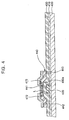
FIG. 1 is a cross-sectional view of a thin film transistor (TFT) according to an embodiment of the present invention; -
FIG. 2 is a cross-sectional view of a semiconductor layer of the TFT shown inFIG. 1 ; -
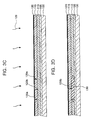
FiGs. 3A through 3G are cross-sectional views illustrating a process of fabricating the TFT shown inFIG. 1 ; -
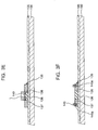
FIG. 4 is a cross-sectional view of a TFT according to another embodiment of the present invention; -
FiGs. 5A through 5D are cross-sectional views illustrating a process of fabricating the TFT shown inFIG. 4 ; -
FIG. 6 is a graph of leakage current loff(A) versus channel ratio (=a channel width W(mm)/a channel length L(µm)) of a conventional TFT using a semiconductor layer crystallized using a crystallization-inducing metal; -
FIG. 7 is a graph of leakage current versus channel ratio of a TFT according to an embodiment of the present invention; -
FIG. 8 is a graph of leakage current loff/W (A/mm) per 1mm of the channel width W of a semiconductor layer versus channel length L (µm) of a TFT according to an embodiment of the present invention; -
FIG. 9 is a graph of a function of a leakage current loff/W (A/mm) per 1 mm of the channel width W of a semiconductor layer and the channel length L (µm) of the TFT, which is obtained using regression analysis based on data shown inFIG. 8 ; and -
FIG. 10 is a cross-sectional view of an organic light emitting diode (OLED) display device including the TFT shown inFIG. 1 . - Reference will now be made in detail to the present embodiments of the present invention, examples of which are illustrated in the accompanying drawings, wherein like reference numerals refer to the like elements throughout. The embodiments are described below in order to explain the aspects of the present invention by referring to the figures.
-
FIG. 1 is a cross-sectional view of a thin film transistor (TFT) according to an embodiment of the present invention, andFIG. 2 is a cross-sectional view of a semiconductor layer of the TFT shown inFIG. 1 . - Referring to
FIG. 1 , asubstrate 100 is provided. Thesubstrate 100 may be a glass as shown in this embodiment substrate or a plastic substrate. Abuffer layer 105 may be disposed on thesubstrate 100. Thebuffer layer 105 may prevent diffusion of moisture or impurities generated in thesubstrate 100 or control the transmission rate of heat during a crystallization process so as to facilitate the crystallization of an amorphous silicon (a-Si) layer. Thebuffer layer 105 may be formed of a single or multiple-layer insulating layer, such as a silicon oxide layer or a silicon nitride layer. - A patterned
semiconductor layer 135 is disposed on thebuffer layer 105. Thesemiconductor layer 135 may be obtained through a crystallization technique using a crystallization-inducing metal such as a metal induced crystallization (MIC) technique, a metal induced lateral crystallization (MILC) technique, or a super grain silicon (SGS) technique. Thesemiconductor layer 135 includes achannel region 136 and source anddrain regions semiconductor layer 135 because the SGS technique may retain a low concentration of a crystallization-inducing metal. - Referring to
FIG. 2 , achannel region 136 of thesemiconductor layer 135 has a length L and a width W. Here, the length L of thechannel region 136 corresponds to a distance between the source and drainregions semiconductor layer 135, and the width W of thechannel region 136 corresponds to a width of thechannel region 136 perpendicular to the distance between the source and drainregions - The length L(µm) of the
channel region 136 of thesemiconductor layer 135 and a leakage current loff(A) per 1 mm of the width W of thechannel region 136 of thesemiconductor layer 135, i.e., the leakage current loff/W as a function of the length L, can be expressed as in Equation 1: -

wherein "c" is a constant ranging from 2.5x10⁻¹³ to 6.8x10⁻¹³. - According to Equation 1, since a leakage current may be predicted according to the size of the
channel region 136 of thesemiconductor layer 135, the leakage current may be controlled using the width W or length L of thechannel region 136 of thesemiconductor layer 135. Conversely, since the leakage current may be predicted, the length L or width W of thechannel region 136 of thesemiconductor layer 135 may be determined considering a leakage current to be controlled. - Referring to
FIG. 9 , when the width W of thechannel region 136 of thesemiconductor layer 135 is constant, as the length L of thechannel region 136 decreases, a leakage current per 1 mm of the width W of thechannel region 136 also decreases because of the more efficient removal of the crystallization-inducing metal from thechannel region 136 using a region where either a metal other than the crystallization-inducing metal or a metal silicide thereof is formed. Noticeably, when the length L of thechannel region 136 is more than 0 and 15µm or less, a value loff/W may be 1.0x10⁻¹²A or less due to a high gettering effect, so that the TFT can exhibit good characteristics in a display device. - Referring back to
FIG. 1 , aregion 145a in which either a metal, the metal being other than the crystallization-inducing metal or a metal silicide thereof is formed is disposed in thesemiconductor layer 135 to a predetermined depth from a surface of thesemiconductor layer 135 and spaced apart from thechannel region 136. In this case, the metal or the metal silicide is used for the gettering process. In the present embodiment, the gettering process is performed using theregion 145a in which the metal or the metal silicide is formed, thereby removing the crystallization-inducing metal from thechannel region 136 of thesemiconductor layer 135. As a result, a leakage current may be reduced and the length L(µm) of thechannel region 136 of thesemiconductor layer 135 and the leakage current loff/W(A/mm) per 1 mm of the width W of thechannel region 136 of thesemiconductor layer 135 may satisfy Equation 1. - A distance between the
channel region 136 and theregion 145a in which either the metal other than the crystallization-inducing metal or the metal silicide thereof is formed may be constant irrespective of the length L of thechannel region 136. In other words, the length L of thechannel region 136 may vary, and the distance between thechannel region 136 and theregion 145a may be constant with respect to the length L of thechannel region 136. - The metal or metal silicide used for the gettering process may have a lower diffusion coefficient than the crystallization-inducing metal in the
semiconductor layer 135. Specifically, the diffusion coefficient of the metal or metal silicide used for the gettering process may be 1% or less of the diffusion coefficient of the crystallization-inducing metal in thesemiconductor layer 135. In this case, the metal or metal silicide used for the gettering process may be prevented from diffusing from theregion 145a into the remaining region of thesemiconductor layer 135. - In general, nickel (Ni) may be used as the crystallization-inducing metal used for the crystallization of the
semiconductor layer 135. Ni has a diffusion coefficient of about 10-5 cm2/s or less in thesemiconductor layer 135. Therefore, when Ni is used as the crystallization-inducing metal, the diffusion coefficient of the metal or metal silicide used for the gettering process may be 1% or less of the diffusion coefficient of Ni. Specifically, the metal or metal silicide may have a diffusion coefficient of 10-7 cm2/s or less. In this case, the metal or metal silicide used for the gettering process may be one selected from the group consisting of Sc, Ti, Zr, Hf, V, Nb, Ta, Cr, Mo, W, Mn, Re, Ru, Os, Co, Rh, Ir, Pt, Y, La, Ce, Pr, Nd, Dy, Ho, TiN, TaN, alloys thereof, and metal silicides thereof. - Continuing in
FIG. 1 , agate insulating layer 150 is disposed on the surface of thesubstrate 100 including thesemiconductor layer 135. Thegate insulating layer 150 may be a silicon oxide layer, a silicon nitride layer, or a double layer thereof. Agate electrode 155 is disposed on a region of thegate insulating layer 150 corresponding to thechannel region 136 of thesemiconductor layer 135. Thegate electrode 155 may be a single layer formed of aluminum (Al) or an Al alloy, such as aluminum-neodymium (Al-Nd), or a multiple layer obtained by stacking an Al alloy layer on a chromium (Cr) alloy layer or a molybdenum (Mo) alloy layer. - An interlayer insulating
layer 160 is disposed on the surface of thesubstrate 100 including thegate electrode 155. The interlayer insulatinglayer 160 may be a silicon nitride layer, a silicon oxide layer, or include multiple layers thereof. - Source and
drain electrodes interlayer insulating layer 160 and electrically connected to the source and drainregions semiconductor layer 135. Thus, the TFT according to the present embodiment is completed. Alternatively, the metal or metal silicide may comprise the same material as thegate electrode 155 or the source and drainelectrodes -
FIGS. 3A through 3G are cross-sectional views illustrating a process of fabricating the TFT shown inFIG. 1 . Referring toFIG. 3A , abuffer layer 105 is formed on asubstrate 100 formed of glass, stainless steel, or plastic. Thebuffer layer 105 may be a single layer or a multiple layer obtained by depositing an insulating layer, such as a silicon oxide layer or a silicon nitride layer, using a chemical vapor deposition (CVD) technique or a physical vapor deposition (PVD) technique. In this case, thebuffer layer 105 may prevent diffusion of moisture or impurities generated in thesubstrate 100 or control the transmission rate of heat during a crystallization process so as to facilitate crystallization of an amorphous silicon (a-Si) layer. Although described as including thebuffer layer 105, thebuffer layer 105 need not be included in all embodiments. - Thereafter, an
a-Si layer 110 is formed on thebuffer layer 105. In this case, thea-Si layer 110 may be formed using a CVD technique or a PVD technique. Also, a dehydrogenation process may be performed during or after the formation of thea-Si layer 110, thereby lowering the concentration of hydrogen therein. - Next, the
a-Si layer 110 is crystallized into a polycrystalline silicon (poly-Si) layer 130 (ofFIG. 3D ). In the present embodiment, the crystallization of thea-Si layer 110 into the poly-Si layer 130 may be performed by a method using a crystallization-inducing metal, such as a metal induced crystallization (MIC) technique, a metal induced lateral crystallization (MILC) technique, or a super grain silicon (SGS) technique. - In the MIC technique, a crystallization-inducing metal, such as nickel (Ni), palladium (Pd), or aluminum (Al), is brought into contact with or injected into the
a-Si layer 110 so that thea-Si layer 110 is crystallized into a poly-Si layer 130 due to the crystallization-inducing metal. In the MILC technique, metal silicide obtained by a reaction between a crystallization-inducing metal and silicon continuously diffuses in a lateral direction so that thea-Si layer 110 is crystallized into a poly-Si layer 130 by sequentially inducing crystallization of the silicon in thea-Si layer 110. - The SGS technique maintains a lower concentration of a crystallization-inducing metal diffusing into the
a-Si layer 110 than in the MIC technique or the MILC technique, so that crystal grains may be controlled to be in the range of several µm to several hundred µm. In an embodiment of the present invention, in order to reduce the concentration of the crystallization-inducing metal diffusing into thea-Si layer 110, a capping layer 115 (ofFIG. 3B ) may be formed on thea-Si layer 110, and a crystallization-inducing metal layer may be formed on the capping layer and annealed so as to diffuse a crystallization-inducing metal. However, thecapping layer 115 may be omitted and a low-concentration crystallization-inducing metal layer may be formed so that the concentration of a crystallization-inducing metal diffusing into thea-Si layer 110 may be reduced. - In the present embodiment, a method of forming a poly-Si layer using a SGS technique will be described.
FIG. 3B is a cross-sectional view of a process of forming thecapping layer 115 and a crystallization-inducing metal on thea-Si layer 110. Referring toFIG. 3B , thecapping layer 115 is formed on thea-Si layer 110. Thecapping layer 115 may be a silicon nitride layer, in which case it is easy to control diffusion of a subsequently formed crystallization-inducing metal during an annealing process. However, thecapping layer 115 may be a double layer of a silicon nitride layer and a silicon oxide layer. Thecapping layer 115 may be formed using a CVD technique or a PVD technique. In this case, thecapping layer 115 may be formed to a thickness of about 0.1 to 200 nm. When thecapping layer 115 is less than 0.1 nm, thecapping layer 115 may not control the amount of the crystallization-inducing metal diffusing into thea-Si layer 110. When thecapping layer 115 is greater than 200 nm, only a small amount of the crystallization-inducing metal diffuses into thea-Si layer 110, thereby precluding crystallization of thea-Si layer 110 into a poly-Si layer 130. - Thereafter, a crystallization-inducing metal is deposited on the
capping layer 115, thereby forming a crystallization-inducingmetal layer 120. The crystallization-inducing metal may be one selected from the group consisting of Ni, Pd, Ag, Au, Al, Sn, Sb, Cu, Tb, and Cd. Ni may be preferred as the crystallization-inducing metal. The crystallization-inducingmetal layer 120 may be formed to an areal density of 1011 to 1015 atoms/cm2 on thecapping layer 115. When the crystallization-inducingmetal layer 120 is formed to an areal density lower than 1011 to 1015 atoms/cm2, it is difficult to crystallize thea-Si layer 110 into a poly-Si layer due to the small number of crystallization nuclei (i.e., seeds). Conversely, when the crystallization-inducingmetal layer 120 is formed to an areal density higher than 1011 to 1015 atoms/cm2, an excessively large amount of the crystallization-inducing metal diffuses into thea-Si layer 110, thereby reducing the size of crystal grains of a poly-Si layer and increasing the amount of the remaining crystallization-inducing metal. As a result, a semiconductor layer obtained by patterning the poly-Si layer may have degraded characteristics. -
FIG. 3C is a cross-sectional view of a process of annealing thesubstrate 100 to diffuse the crystallization-inducing metal via thecapping layer 115 to an interface between thecapping layer 115 and thea-Si layer 110. Referring toFIG. 3C , thesubstrate 100 on which thebuffer layer 105, thea-Si layer 110, thecapping layer 115, and the crystallization-inducingmetal layer 120 are formed is annealed (as indicated by reference numeral 125) so as to diffuse part of the crystallization-inducing metal of the crystallization-inducingmetal layer 120 into the surface of thea-Si layer 110. Specifically, out of a crystallization-inducingmetal metal 120b diffuses into thea-Si layer 110, and a large amount of the crystallization-inducingmetal 120a may neither reach the a-Si layer nor pass through thecapping layer 115. - Therefore, the amount of the crystallization-inducing
metal 120b that reaches the surface of thea-Si layer 110 depends on the diffusion barrier capability of thecapping layer 115, which is closely associated with the thickness and density of thecapping layer 115. Specifically, as the thickness or density of thecapping layer 115 increases, the amount of the crystallization-inducingmetal 120b that diffuses into thea-Si layer 110 decreases, and thus the size of crystal grains of a poly-Si layer 130 increases. Conversely, as the thickness or density of thecapping layer 115 decreases, the amount of the crystallization-inducingmetal 120b that diffuses into thea-Si layer 110 increases, and thus the size of the crystal grains of the poly-Si layer 130 decreases. - In order to prevent deformation of the
substrate 100, the annealing process for diffusing the crystallization-inducing metal is performed at a temperature of about 200 to 900°C for several seconds to several hours in consideration of the fabrication cost and yield. The annealing process may be one of a furnace process, a rapid thermal annealing (RTA) process, an ultraviolet (UV) process, and a laser process. -
FIG. 3D is a cross-sectional view of a process of crystallizing thea-Si layer 110 into a poly-Si layer 130 due to the diffused crystallization-inducing metal. Referring toFIG. 3D , thea-Si layer 110 is crystallized into the poly-Si layer 130 due to the crystallization-inducingmetal 120b that passes through thecapping layer 115 and diffuses into the surface of thea-Si layer 110. Specifically, the diffused crystallization-inducingmetal 120b combines with silicon (Si) of thea-Si layer 110 to form metal silicide as crystallization nuclei (i.e., seeds). Thus, thea-Si layer 110 is crystallized into the poly-Si layer 130 using the seeds. - Meanwhile, although
FIG. 3D illustrates that the annealing process is performed on the resultant structure from which thecapping layer 115 and the crystallization-inducingmetal layer 120 are not removed, aspects of the present invention is not limited thereto. That is, after the crystallization-inducing metal is diffused into thea-Si layer 110 to form metal silicide, thecapping layer 115 and the crystallization-inducingmetal layer 120 may be removed and the resultant structure may be annealed to form the poly-Si layer 130. - Referring to
FIG. 3E , thecapping layer 115 and the crystallization-inducingmetal layer 120 are removed, and the poly-Si layer 130 is patterned to form asemiconductor layer 135. Unlike in the present embodiment, the poly-Si layer 130 may be patterned during a subsequent process. - Here, a length and width of the
semiconductor layer 135 are determined in consideration of Equation 1: -

wherein "c" is a constant ranging from 2.5x10⁻¹³ to 6.8x10⁻¹³. Specifically, a length L and a width W of achannel region 136 of thesemiconductor layer 135 are determined according to a leakage current to be controlled, and the length and width of thesemiconductor layer 135 are determined in consideration of the length L and width W of thechannel region 136. - Referring to
FIG. 9 , when the width W of the channel region of thesemiconductor layer 135 is constant, as the length L of thechannel region 136 decreases, a leakage current per 1 mm of the width W of the channel region also decreases because of more efficient removal of the crystallization-inducing metal from the channel region using a subsequent metal layer or metal silicide layer used for a gettering process. Noticeably, when the length L of thechannel region 136 is more than 0 and 15µm or less, a value loff/W can be 1.0x10⁻¹²A or less due to a high gettering effect so that the resultant TFT can exhibit good characteristics as a display device. - Thereafter, a
photoresist pattern 140 is formed on a region of thesemiconductor layer 135 where achannel region 136 will be defined. Conductive impurity ions are doped into thesemiconductor layer 135 using thephotoresist pattern 140 as a mask, thereby forming asource region 137, adrain region 138, and achannel region 136 having a length L and a width W. In this case, the impurity ions may be p-type impurity ions or n-type impurity ions. The p-type impurity ions may be ions of one selected from the group consisting of boron (B), aluminum (Al), gallium (Ga), and indium (In), and the n-type impurity ions may be ions of one selected from the group consisting of phosphorus (P), arsenic (Ar), and antimony (Sb). - Referring to
FIG. 3F , thephotoresist pattern 140 is removed, and a metal layer pattern or metalsilicide layer pattern 145 is formed a predetermined distance apart from thechannel region 136. The metal layer pattern or metalsilicide layer pattern 145 is in contact with a region of thesemiconductor layer 135 other than thechannel region 136. In the present embodiment, depositing the metal layer pattern or metalsilicide layer pattern 145 is followed by performing an annealing process to form aregion 145a in thesemiconductor layer 135, and a gettering process is performed using theregion 145a. Thus, the crystallization-inducing metal is removed from thechannel region 136 of thesemiconductor layer 135 so that a leakage current may be reduced and the length L of thechannel region 136 of thesemiconductor layer 135 and the leakage current loff/W(A/mm) per 1 mm of the width W of thechannel region 136 of thesemiconductor layer 135 may satisfy Equation 1. - The position of the metal layer pattern or metal
silicide layer pattern 145 may be constant irrespective of the length L of thechannel region 136. In other words, the length L of thechannel region 136 may vary, and the metal layer pattern or metalsilicide layer pattern 145 may be formed such that a distance between thechannel region 136 and the metal layer pattern or metalsilicide layer pattern 145 is constant with respect to the length L of thechannel region 136. - The metal layer pattern or metal
silicide layer pattern 145 for gettering in thesemiconductor layer 135 may be a metal layer pattern or metal silicide layer pattern including a metal or alloy thereof having a diffusion coefficient less than the crystallization-inducingmetal - The diffusion coefficient of the metal or metal silicide of the metal layer pattern or metal
silicide layer pattern 145 in thesemiconductor layer 135 may be 1% or less of the diffusion coefficient of the crystallization-inducingmetal silicide layer pattern 145 may be prevented from diffusing from theregion 145a into the remaining region of thesemiconductor layer 135. - In general, Ni may be used as the crystallization-inducing
metal semiconductor layer 135. Ni has a diffusion coefficient of about 10-5 cm2/s or less in thesemiconductor layer 135. Therefore, when Ni is used as the crystallization-inducingmetal silicide layer pattern 145 used for gettering in thesemiconductor layer 135 may be 1% or less of the diffusion coefficient of Ni. Specifically, the metal or metal silicide may have a diffusion coefficient of 10-7 cm2/s or less. In this case, the metal or metal silicide may be one selected from the group consisting of Sc, Ti, Zr, Hf, V, Nb, Ta, Cr, Mo, W, Mn, Re, Ru, Os, Co, Rh, Ir, Pt, Y, La, Ce, Pr, Nd, Dy, Ho, TiN, TaN, alloys thereof, and metal silicides thereof. - Also, the metal layer pattern or metal
silicide layer pattern 145 may be formed to a thickness of about 3 to 1000 nm. When the metal layer pattern or metalsilicide layer pattern 145 is formed to a thickness of less than about 3 nm, the crystallization-inducing metal may inefficiently getter into theregion 145a of thesemiconductor layer 135 that contacts the metal layer pattern or metalsilicide layer pattern 145. When the metal layer pattern or metalsilicide layer pattern 145 is formed to a thickness of more than about 1000 nm, the metal layer pattern or metalsilicide layer pattern 145 may be delaminated due to thermal stress during a subsequent annealing process. - Thereafter, an annealing process is performed in order to remove the crystallization-inducing
metal 120b, from thesemiconductor layer 135, especially, thechannel region 136 of thesemiconductor layer 135. As a result, a metal of the metal layer pattern may diffuse from the surface of thesemiconductor layer 135 that contacts the metal layer pattern or metalsilicide layer pattern 145 into thesemiconductor layer 135 or combine with thesemiconductor layer 135 to form a metal silicide. Alternatively, a metal silicide of the metal silicide layer pattern diffuses into thesemiconductor layer 135. Thus, theregion 145a containing a metal other than the crystallization-inducing metal or a metal silicide thereof, is formed in a region of thesemiconductor layer 135 that contacts the metal layer pattern or metalsilicide layer pattern 145. - When the crystallization-inducing metal remaining in the
channel region 136 of thesemiconductor layer 135 diffuses into theregion 145a of thesemiconductor layer 135 that contacts the metal layer pattern or metalsilicide layer pattern 145 due to the annealing process, the crystallization-inducingmetal 120b is precipitated in theregion 145a and does not diffuse any more. This is because the crystallization-inducingmetal 120b is thermodynamically more stable in theregion 145a containing the other metal or a metal silicide thereof than in silicon. Based on this principle, the crystallization-inducingmetal 120b may be removed from thechannel region 136 of thesemiconductor layer 135. - In this case, the annealing process may be performed at a temperature of about 500 to 993°C for 10 seconds to 10 hours. When the annealing process is performed at a temperature lower than 500°C, diffusion of the crystallization-inducing metal into the
semiconductor layer 135 does not occur so that the crystallization-inducingmetal 120b cannot move to theregion 145a of thesemiconductor layer 135. When the annealing process is performed at a temperature higher than 993°C and Ni is used as the crystallization-inducingmetal substrate 100 may be deformed due to high heat. - Also, when the annealing process is performed for a time shorter than 10 seconds, it may be difficult to sufficiently remove the crystallization-inducing
metal 120b from thechannel region 136 of thesemiconductor layer 135. When the annealing process is performed for a time longer than 10 hours, the long-duration annealing process gives rise to deformation of thesubstrate 100, increases the fabrication cost, and may decrease yield. Meanwhile, when the annealing process is performed at a sufficiently high temperature, it is possible to remove the crystallization-inducingmetal 120b in a short time. - Referring to
FIG. 3G , the metal layer pattern or metalsilicide layer pattern 145 is removed, and agate insulating layer 150 is formed on the surface of thesubstrate 100 having thesemiconductor layer 135. Thegate insulating layer 150 may be a silicon oxide layer, a silicon nitride layer, or a multi-layer thereof. - Thereafter, a metal layer (not shown) for a gate electrode is formed. The metal layer may be a single layer formed of AI or an Al alloy, such as Al-Nd, or a multiple layer formed by stacking an Al alloy on a Cr alloy or a Mo alloy. Photolithographic and etching processes are performed on the metal layer for the gate electrode, thereby forming a
gate electrode 155 to correspond to thechannel region 136 of thesemiconductor layer 135. - Subsequently, an
interlayer insulating layer 160 is formed on the surface of thesubstrate 100 having thegate electrode 155. The interlayer insulatinglayer 160 may be a silicon nitride layer, a silicon oxide layer, or a multiple layer thereof. - The interlayer insulating
layer 160 and thegate insulating layer 150 are etched to form contact holes to expose the source and drainregions semiconductor layer 135. Source anddrain electrodes regions electrodes semiconductor layer 135, thegate electrode 155, and the source and drainelectrodes - Alternatively, the metal layer pattern or metal
silicide layer pattern 145 and thegate electrode 155 or the source and drainelectrodes silicide layer pattern 145 may be simultaneously formed when thegate electrode 155 or the source and thedrain electrodes -
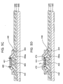
FIG. 4 is a cross-sectional view of a TFT according to another embodiment of the present invention. The TFT shown inFIG. 4 is generally the same as the TFT shown inFIGs. 1 and2 except for the following description. - Referring to
FIG. 4 , asubstrate 400 is prepared. Abuffer layer 410 may be disposed on thesubstrate 400, as shown in this embodiment. Agate electrode 420 is disposed on thebuffer layer 410. Agate insulating layer 430 is disposed on thegate electrode 420. - A patterned
semiconductor layer 440 is disposed on thegate insulating layer 430. Thesemiconductor layer 440 is a semiconductor layer crystallized by a method using a crystallization-inducing metal, such as an MIC technique, an MILC technique, or an SGS technique. Thesemiconductor layer 440 includes achannel region 441 and source and drainregions semiconductor layer 440 because the SGS technique may maintain a low concentration of a crystallization-inducing metal diffusing into an a-Si layer. - A length L(µm) of the
channel region 441 of thesemiconductor layer 440 and a leakage current loff(A) per 1 mm of a width W of thechannel region 441 of thesemiconductor layer 440 satisfy Equation 1: -

wherein "c" is a constant ranging from 2.5x10⁻³ to 6.8x10⁻¹³. - Based on Equation 1, since a leakage current may be predicted according to the size of the
channel region 441 of thesemiconductor layer 440, the leakage current may be controlled using the width W or length L of thechannel region 441 of thesemiconductor layer 440. Conversely, since the leakage current may be predicted, the length L or width W of thechannel region 441 of thesemiconductor layer 440 may be determined considering a leakage current to be controlled. - Referring to
FIG. 9 , when the width W of thechannel region 441 of thesemiconductor layer 440 is constant, as the length L of thechannel region 441 decreases, a leakage current per 1 mm of the width W of thechannel region 441 also decreases because of the more efficient removal of the crystallization-inducing metal from thechannel region 441 using a region in which a metal other than the crystallization-inducing metal or metal silicide thereof is formed. Noticeably, when the length L of thechannel region 441 is more than 0 and 15µm or less, a value loff/W can be 1.0x10⁻¹² A/mm or less due to a high gettering effect, so that the TFT can exhibit good characteristics in a display device. - A
region 460a in which either a metal other than the crystallization-inducing metal or a metal silicide thereof is formed is disposed to a predetermined depth from the surface of thesemiconductor layer 135 in thesemiconductor layer 440 and spaced apart from thechannel region 441. In this case, the metal or the metal silicide is used for a gettering process. In the present embodiment, a gettering process is performed using theregion 460a in which the metal or the metal silicide is formed, thereby removing the crystallization-inducing metal from thechannel region 441 of thesemiconductor layer 440. As a result, a leakage current may be reduced and the length L(µm) of thechannel region 441 of thesemiconductor layer 440 and the leakage current loff(A) per 1 mm of the width W of thechannel region 441 of thesemiconductor layer 440 may satisfy Equation 1. - A distance between the
channel region 441 and theregion 460a in which either the metal other than the crystallization-inducing metal or the metal silicide thereof is formed may be constant irrespective of the length L of thechannel region 441. - Source and
drain electrodes semiconductor layer 440 and electrically connected to the source and drainregions semiconductor layer 440. Thus, the TFT according to the present embodiment is completed. -
FIGS. 5A through 5D are cross-sectional views of a process of fabricating the TFT shown inFIG. 4 . The process shown inFIGs. 5A through 5D is generally the same as the process shown inFIGs. 3A through 3G except for the following description. - Referring to
FIG. 5A , abuffer layer 410 is formed on asubstrate 400. A metal layer (not shown) for a gate electrode is formed on thebuffer layer 410 and etched using photolithographic and etching processes, thereby forming agate electrode 420. Agate insulating layer 430 is formed on thesubstrate 400 having thegate electrode 420. - Referring to
FIG. 5B , an a-Si layer is formed on thegate insulating layer 430 and crystallized into a poly-Si layer using a crystallization-inducing metal as in the previous embodiment. The poly-Si layer is patterned to form asemiconductor layer 440. The poly-Si layer may be patterned during a subsequent process. - Here, a length and width of the
semiconductor layer 135 are determined in consideration of Equation 1: -

wherein "c" is a constant ranging from 2.5x10⁻¹³ to 6.8x10⁻¹³. Specifically, a length L and a width W of a channel region of thesemiconductor layer 440 are determined according to a leakage current to be controlled, and the length and width of thesemiconductor layer 440 are determined in consideration of the length L and width W of the channel region. - Referring to
FIG. 9 , when the width W of the channel region of thesemiconductor layer 440 is constant, as the length L of the channel region decreases, a leakage current per 1 mm of the width W of the channel region also decreases because of the more efficient removal of the crystallization-inducing metal from the channel region using a subsequent metal layer or metal silicide layer used for a gettering process. Noticeably, when the length L of the channel region is more than 0 and 15µm or less, a value loff/W can be 1.0x10⁻¹² A/mmor less due to a high gettering effect, so that the resultant TFT can exhibit good characteristics in a display device. - Thereafter, a
photoresist pattern 450 is formed on a region of thesemiconductor layer 440 where a channel region will be defined. Conductive impurity ions are doped into thesemiconductor layer 440 using thephotoresist pattern 450 as a mask, thereby forming asource region 442, adrain region 443, and achannel region 441 having a length L and a width W. - Referring to
FIG. 5C , thephotoresist pattern 450 is removed, and a metal layer pattern or metalsilicide layer pattern 460 is formed a predetermined distance apart from thechannel region 441. The metal layer pattern or metalsilicide layer pattern 460 is in contact with a region of thesemiconductor layer 440 other than thechannel region 441. - In the present embodiment, depositing the metal layer pattern or metal
silicide layer pattern 460 is followed by performing an annealing process to form aregion 460a in thesemiconductor layer 440, and a gettering process is performed using theregion 460a. Thus, the crystallization-inducing metal is removed from thechannel region 136 of thesemiconductor layer 135 so that a leakage current may be reduced and the length L of thechannel region 136 of thesemiconductor layer 135 and the leakage current loff(A) per 1 mm of the width W of thechannel region 136 of thesemiconductor layer 135 may satisfy Equation 1. - The position of the metal layer pattern or metal
silicide layer pattern 460 may be constant irrespective of the length L of thechannel region 441. In other words, the length L of thechannel region 441 may vary, and the metal layer pattern or metalsilicide layer pattern 460 may be formed such that a distance between thechannel region 441 and the metal layer pattern or metalsilicide layer pattern 460 is constant with respect to the length L of thechannel region 441. - Thereafter, an annealing process is performed in order to remove the crystallization-inducing metal from the
semiconductor layer 440, especially, thechannel region 441 of thesemiconductor layer 440. As a result, aregion 460a containing a metal other than the crystallization-inducing metal or a metal silicide thereof is formed in a region of thesemiconductor layer 440 that contacts the metal layer pattern or metalsilicide layer pattern 460. Theregion 460a is formed in the surface of thesemiconductor layer 440 to a predetermined depth. The crystallization-inducing metal existing in thechannel region 441 of thesemiconductor layer 440 is gettered by diffusion into theregion 460a. The annealing process is performed in a similar manner as described above. - Referring to
FIG. 5D , the metal layer pattern or metalsilicide layer pattern 460 is removed, and a source/drain conductive layer is formed on thesemiconductor layer 440 and patterned, thereby forming source and drainelectrodes gate electrode 420, thesemiconductor layer 440, and the source and drainelectrodes -
FIG. 6 is a graph of leakage current loff(A) versus channel ratio (i.e., a channel width W(mm)/a channel length L(µm)) of a conventional TFT using a semiconductor layer crystallized using a crystallization-inducing metal. InFIG. 6 , the abscissa denotes the channel ratio (i.e., the channel width W(mm)/the channel length L(µm)), and the ordinate denotes the leakage current loff(A). - Referring to
FIG. 6 , it can be seen that the leakage current loff(A) of the conventional TFT using the semiconductor layer crystallized using the crystallization-inducing metal shows no tendency but irregularly increases or decreases when the channel width W is 4, 10, and 50 mm, respectively, or when the channel length L ranges from 3 to 20 µm. Also, even if the channel ratio varies, the leakage current loff(A) varies within only a small range from 2.0x10⁻¹² to 4.0x10⁻¹²A, which makes no significant difference. Therefore, it can be seen that in the conventional TFT, the leakage current loff(A) is not effectively controlled by changing the channel ratio. Thus, unlike in a TFT according to an embodiment of the present invention, in the conventional TFT using the semiconductor layer crystallized using the crystallization-inducing metal, it is difficult to predict a change in the leakage current loff(A) according to the channel ratio, or to precisely control the leakage current by changing the channel ratio. Conversely, the size of a channel region cannot be determined considering a leakage current loff(A) to be controlled. -
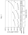
FIG. 7 is a graph of leakage current loff(A) versus channel ratio of a TFT according to an embodiment of the present invention in which a metal layer pattern or metal silicide layer pattern for a gettering process is formed and annealed. InFIG. 7 , an abscissa denotes the channel ratio (=the channel width W(mm)/the channel length L(µm)), and an ordinate denotes the leakage current loff(A). - Referring to
FIG. 7 , even if the TFT according to this embodiment of the present invention has the same channel ratio as the conventional TFT described with reference toFIG. 6 , the leakage current loff(A) was greatly reduced to approximately 5.0x10⁻¹³A. That is, when the metal layer pattern or metal silicide layer pattern for the gettering process is formed and annealed, it can be confirmed that a crystallization-inducing metal existing in a channel region is gettered. -
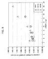
FIG. 8 is a graph of leakage current loff (A) per 1mm of the channel width W of a semiconductor layer versus channel length L (µm) of a TFT according to an embodiment of the present invention. InFIG. 8A , the abscissa denotes the channel length L(µm), and the ordinate denotes the leakage current loff (A) per 1 mm of the channel width W. - In order to comprehend a correlation between the channel length L of the TFT according to the exemplary embodiment of the present invention and a leakage current loff(A), the leakage current loff shown in
FIG. 7 is divided by the channel width W, andFIG. 8 shows leakage current loff/W divided by the channel width W versus channel length L. As a result, it can be seen that as the channel length L increases, the value loff/W increases according to the curve shown inFIG. 8 . That is, when the channel width W is constant, as the channel length L increases, the leakage current loff increases according to the curve ofFIG. 8 , which is a quadratic function. -
FIG. 9 is a graph of a function of a leakage current loff(A) per 1 mm of the channel width W of a semiconductor layer and the channel length L (µm) of the TFT, which is obtained using regression analysis based on data shown inFIG. 8 . InFIG. 9 , the abscissa denotes the channel length L (µm), and the ordinate denotes the leakage current loff(A) per 1 mm of the channel width W. - Referring to
FIG. 9 , loff/W=(3.4x10-15)L2+(2.4x10-12)L+2.5x10-13 to 6.8x10⁻¹³ is obtained using regression analysis and is a function correlating the leakage current loff/W and the channel length L based on data shown inFIG. 8 . Here, the leakage current loff, the channel width W, and the channel length L are expressed in units of A, mm, and µm, respectively. - Accordingly, in the TFT according to embodiments of the present invention, the crystallization-inducing metal may be removed from the channel region of the semiconductor layer, thereby reducing the leakage current. Also, since the leakage current may be predicted according to the size of the channel region of the semiconductor layer, the leakage current may be determined by controlling the width W or length L of the channel region of the semiconductor layer. Conversely, the length L or width W of the channel region of the semiconductor layer may be determined considering the leakage current to be controlled.
- Furthermore, referring to
FIG. 9 , in the TFT according to the embodiments of the present invention, when the width W of the channel region of the semiconductor layer is constant, as the length L of the channel region decreases, a leakage current per 1 mm of the width W of the channel region also decreases according to a secondary functional curve because of the more efficient removal of the crystallization-inducing metal from the channel region using the metal layer pattern or metal silicide layer pattern for a gettering process. In particular, when the length L of the channel region is more than 0 and 15µm or less, the value loff/W can be 1.0x10⁻¹²A or less due to a high gettering effect, so that the resultant TFT can exhibit good characteristics as a display device. -
FIG. 10 is a cross-sectional view of an organic light emitting diode (OLED) display device including the TFT shown inFIG. 1 . Although aspects of the present invention are described with reference to an OLED, the aspects of the present invention are not limited thereto such that the TFT according to aspects of the present invention may be used in other display devices, such as a liquid crystal display or a plasma display panel, among others. Referring toFIG. 10 , an insulatinglayer 170 is formed on the surface of thesubstrate 100 having the TFT shown inFIG. 3G , according to the present embodiment. The insulatinglayer 170 may be an inorganic layer selected from the group consisting of a silicon oxide layer, a silicon nitride layer, and a silicon on glass (SOG) layer, an organic layer formed of one selected from the group consisting of polyimide, benzocyclobutene (BCB) series resin, and acrylate, or a stacked layer of the inorganic layer and the organic layer. - The insulating
layer 170 may be etched to form a via hole exposing one of the source and drainelectrodes first electrode 175 is formed and connected to one of the source and drainelectrodes first electrode 175 may be an anode or a cathode. When thefirst electrode 175 is an anode, the anode may be formed of a transparent conductive material selected from the group consisting of indium tin oxide (ITO), indium zinc oxide (IZO), and indium tin zinc oxide (ITZO). When thefirst electrode 175 is a cathode, the cathode may be formed of one selected from the group consisting of Mg, Ca, Al, Ag, Ba, and alloys thereof. - Thereafter, a
pixel defining layer 180 is formed on thefirst electrode 175 to have an opening that exposes a portion of thefirst electrode 175. Anorganic layer 185 including an emission layer (EML) is formed on the exposed portion of thefirst electrode 175. Theorganic layer 185 may further include a hole injection layer (HIL), a hole transport layer (HTL), a hole blocking layer (HBL), an electron blocking layer (EBL), an electron injection layer (EIL), and an electron transport layer (ETL), among other layers. After that, asecond electrode 190 is formed on theorganic layer 185. As a result, the fabrication of the OLED according to the present embodiment is completed. - In the TFT according to this embodiment of the present invention, a region in which either a metal other than a crystallization-inducing metal or a metal silicide thereof is formed is disposed in a semiconductor layer crystallized using the crystallization-inducing metal. The region in which the metal or metal silicide is formed is spaced apart from a channel region of the semiconductor layer and extends from the surface of the semiconductor layer to a predetermined depth. In the present embodiment, a gettering process is performed using the region in which the metal or the metal silicide is formed, thereby removing the crystallization-inducing metal from the channel region of the semiconductor layer. As a result, a leakage current may be decreased. Also, since the leakage current may be predicted according to the size of the channel region of the semiconductor layer, the leakage current may be determined by controlling the width W or length L of the channel region of the semiconductor layer. Conversely, the width W or length L of the channel region of the semiconductor layer may be determined considering a leakage current to be controlled.
- According to aspects of the present invention as described above, in a TFT including a semiconductor layer crystallized using a crystallization-inducing metal, the crystallization-inducing metal can be removed from a channel region of the semiconductor layer. As a result, a leakage current can be reduced. Also, the leakage current can be predicted according to the width or length of the channel region of the semiconductor layer. Furthermore, the width or length of the channel region of the semiconductor layer may be determined considering a leakage current to be controlled.
- Further, although aspects of the present invention are described in association with an organic light emitting diode display devices, the aspects of the present invention are not limited thereto such that the thin film transistor according to the aspects of the present invention may be used with other display devices, such as liquid crystal displays and plasma display paneis.
- Although a few embodiments of the present invention have been shown and described, it would be appreciated by those skilled in the art that changes may be made in this embodiment without departing from the principles of the invention, the scope of which is defined in the claims and their equivalents.
Claims (18)
- A thin film transistor, comprising:a substrate;a semiconductor layer disposed on the substrate and crystallized using a crystallization-inducing metal, the semiconductor layer including a channel region and source and drain regions, and the semiconductor layer having a predetermined leakage current determined according to a length and a width of the channel region or having a predetermined length and a predetermined width determined according to a leakage current of the semiconductor layer;a gate electrode disposed to correspond to a predetermined region of the semiconductor layer;a gate insulating layer disposed between the gate electrode and the semiconductor layer to insulate the semiconductor layer from the gate electrode;source and drain electrodes respectively electrically connected to the source and drain regions of the semiconductor layer;a metal other than the crystallization-inducing metal or a silicide of a metal other than the crystallization-inducing metal disposed at a predetermined depth from a surface of the semiconductor layer in a region spaced apart from the channel region in the semiconductor layer.
- A thin film transistor according to Claim 1, wherein the length and the width of the channel region of the semiconductor layer and the leakage current of the semiconductor layer satisfy the following equation:

wherein loff (A) is the leakage current of the semiconductor layer, W (mm) is the width of the channel region, L (µm) is the length of the channel region, and "c" is a constant ranging from 2.5x10⁻¹³ to 6.8x10⁻¹³. - A thin film transistor according to claim 1 or 2, wherein the length of the channel region of the semiconductor layer is more than 0 and less that or equal to 15µm.
- A thin film transistor according to any one of claims 1 to 3, wherein the metal other than the crystallization-inducing metal or the metal silicide has a lower diffusion coefficient than the crystallization-inducing metal in the semiconductor layer.
- A thin film transistor according to claim 4, wherein the diffusion coefficient of the metal other than the crystallization-inducing metal or the metal silicide is 1% or less of the diffusion coefficient of the crystallization-inducing metal in the semiconductor layer.
- A thin film transistor according to claim 5, wherein the crystallization-inducing metal comprises nickel (Ni), and the metal other than Ni or the metal silicide has a diffusion coefficient higher than 0 and equal to or lower than 10-7 cm2/s.
- A thin film transistor according to claim 5 or 6, wherein the metal other than the crystallization-inducing metal or the metal silicide comprises one selected from the group consisting of Sc, Ti, Zr, Hf, V, Nb, Ta, Cr, Mo, W, Mn, Re, Ru, Os, Co, Rh, Ir, Pt, Y, La, Ce, Pr, Nd, Dy, Ho, TiN, TaN, alloys thereof, and metal silicides thereof.
- A thin film transistor according to any one of claims 1 to 7, wherein the semiconductor layer is crystallized using a super grain silicon (SGS) technique.
- A thin film transistor according to any one of claims 1 to 8, wherein the metal other than the crystallization-inducing metal or the metal silicide of the metal comprises the same material as the gate electrode or the source and drain electrodes.
- A method of fabricating a thin film transistor, comprising:crystallizing an amorphous silicon (a-Si) layer into a polycrystalline silicon (poly-Si) layer using a crystallization-inducing metal;determining a length and a width of the channel region of a semiconductor layer according to a predetermined leakage current;patterning the poly-Si layer to form a semiconductor layer having a channel region with a determined length and a determined width; andgettering the crystallization-inducing metal from the channel region with a metal other than the crystallization-inducing metal or a silicide of a metal other than the crystallization metal.
- A method of fabricating a thin film transistor according to claim 10, further comprising:providing a substrate;forming the amorphous silicon (a-Si) layer on the substrate;forming a metal layer pattern or a metal silicide layer pattern spaced apart from the channel region by a predetermined distance to contact a region of the semiconductor layer other than the channel region, the metal layer being of a metal different from the crystallization-inducing metal, and the metal silicide being a silicide of a metal different from the crystallization-inducing metal;annealing the substrate to getter the crystallization-inducing metal from the channel region of the semiconductor layer into a region of the semiconductor layer corresponding to the metal layer pattern or the metal silicide layer pattern;removing the metal layer pattern or the metal silicide layer pattern;forming a gate electrode to correspond to a predetermined region of the semiconductor layer;forming a gate insulating layer between the gate electrode and the semiconductor layer to insulate the semiconductor layer from the gate electrode; andforming source and drain electrodes electrically connected to source and drain regions of the semiconductor layer, respectively.
- A method according to any one of claims 10 to 11, further comprising determining the length and the width of the channel region of the semiconductor layer according to a leakage current to be controlled using the following equation:

wherein loff is the leakage current (A) of the semiconductor layer, W is the width (mm) of the channel region, L is the length (µm) of the channel region, and "c" is a constant ranging from 2.5x10⁻¹³ to 6.8x10⁻¹³. - A method according to claim 11 or any claim when dependent on claim 11, wherein annealing the substrate is performed at a temperature of about 500 to 993°C for 10 seconds to 10 hours.
- A method according to any one of claims 10 to 13, wherein crystallizing the a-Si layer into the poly-Si layer is performed using a super grain silicon (SGS) technique.
- A method according to claim 11 or any claim when dependent on claim 11, wherein the metal layer pattern or the metal silicide layer pattern is formed to a thickness of about 3 to 1000 nm.
- A method according to any one of claims 10 to 15, wherein the channel region of the semiconductor layer is formed to have a length more than 0 and equal to or less than 15µm.
- A display device, comprising a TFT as set out in any one of claims 1 to 9, wherein the display device comprises a first electrode electrically connected to one of the source and drain electrodes;
- A display device according to claim 17, wherein the display further comprises:an organic layer including an emission layer disposed on the first electrode; anda second electrode disposed on the organic layer.
Applications Claiming Priority (1)
| Application Number | Priority Date | Filing Date | Title |
|---|---|---|---|
| KR1020070057900A KR100848341B1 (en) | 2007-06-13 | 2007-06-13 | Thin film transistor, fabricating method of the thin film transistor, and organic lighting emitting diode display device comprising the same |
Publications (2)
| Publication Number | Publication Date |
|---|---|
| EP2003695A2 true EP2003695A2 (en) | 2008-12-17 |
| EP2003695A3 EP2003695A3 (en) | 2011-08-10 |
Family
ID=39791336
Family Applications (1)
| Application Number | Title | Priority Date | Filing Date |
|---|---|---|---|
| EP08252041A Withdrawn EP2003695A3 (en) | 2007-06-13 | 2008-06-13 | Thin film transistor, method of fabricating the thin film transistor, and display device including the thin film transistor |
Country Status (6)
| Country | Link |
|---|---|
| US (1) | US7838885B2 (en) |
| EP (1) | EP2003695A3 (en) |
| JP (1) | JP5091017B2 (en) |
| KR (1) | KR100848341B1 (en) |
| CN (1) | CN101325220B (en) |
| TW (1) | TWI377681B (en) |
Cited By (6)
| Publication number | Priority date | Publication date | Assignee | Title |
|---|---|---|---|---|
| EP2146371A1 (en) * | 2008-07-14 | 2010-01-20 | Samsung Mobile Display Co., Ltd. | Thin film transistor, method of fabricating the same, and organic light emitting diode display device including the thin film transistor |
| US8101952B2 (en) | 2008-03-27 | 2012-01-24 | Samsung Mobile Display Co., Ltd. | Thin film transistor, method of fabricating the same, and organic lighting emitting diode display device including the same |
| US8283668B2 (en) | 2007-08-23 | 2012-10-09 | Samsung Display Co., Ltd. | Thin film transistor, method of fabricating the same, and organic light emitting diode display device including the same |
| US8318523B2 (en) | 2008-04-11 | 2012-11-27 | Samsung Display Co., Ltd. | Thin film transistor, method of fabricating the same and organic light emitting diode display device having the same |
| US8513669B2 (en) | 2007-08-22 | 2013-08-20 | Samsung Display Co., Ltd. | Thin film transistor including metal or metal silicide structure in contact with semiconductor layer and organic light emitting diode display device having the thin film transistor |
| US8790967B2 (en) | 2007-05-31 | 2014-07-29 | Samsung Display Co., Ltd. | Method of fabricating polycrystalline silicon layer, TFT fabricated using the same, method of fabricating TFT, and organic light emitting diode display device having the same |
Families Citing this family (12)
| Publication number | Priority date | Publication date | Assignee | Title |
|---|---|---|---|---|
| KR101043953B1 (en) | 2009-05-29 | 2011-06-24 | 전자부품연구원 | Manufacturing method of thin film transistor and thin film transistor manufacturing by the same |
| KR101293261B1 (en) | 2009-10-21 | 2013-08-09 | 가부시키가이샤 한도오따이 에네루기 켄큐쇼 | Display device and electronic device including display device |
| KR101751560B1 (en) | 2009-11-13 | 2017-06-27 | 가부시키가이샤 한도오따이 에네루기 켄큐쇼 | Semiconductor device |
| TWI555205B (en) | 2010-11-05 | 2016-10-21 | 半導體能源研究所股份有限公司 | Semiconductor device and method for manufacturing the same |
| CN102810569A (en) * | 2011-06-01 | 2012-12-05 | 广东中显科技有限公司 | Polycrystalline silicon thin film transistor capable of driving in nickel and adjusting threshold voltage simultaneously |
| KR101809661B1 (en) * | 2011-06-03 | 2017-12-18 | 삼성디스플레이 주식회사 | Thin film transistor, manufacturing method of thin film transistor, and organic light emitting diode display including the same |
| KR102239841B1 (en) * | 2014-08-06 | 2021-04-14 | 삼성디스플레이 주식회사 | Thin film transistor, display apparatus comprising the same, method for manufacturing thin film transistor, and method for manufacturing display apparatus |
| CN104143533B (en) * | 2014-08-07 | 2017-06-27 | 深圳市华星光电技术有限公司 | High-res AMOLED backboard manufacture methods |
| CN107533979B (en) * | 2015-04-20 | 2020-11-10 | 堺显示器制品株式会社 | Manufacturing method of thin film transistor and display panel |
| CN106298547A (en) * | 2016-08-12 | 2017-01-04 | 烟台南山学院 | A kind of efficient method for annealing of novel amorphous oxide thin film transistor |
| CN106356378B (en) | 2016-09-26 | 2023-10-27 | 合肥鑫晟光电科技有限公司 | Array substrate and manufacturing method thereof |
| CN110391264A (en) * | 2018-04-19 | 2019-10-29 | 群创光电股份有限公司 | Electronic device |
Citations (8)
| Publication number | Priority date | Publication date | Assignee | Title |
|---|---|---|---|---|
| EP0862201A2 (en) * | 1997-02-26 | 1998-09-02 | Semiconductor Energy Laboratory Co., Ltd. | Method of manufacturing a thin film transistor |
| US6156628A (en) * | 1997-07-22 | 2000-12-05 | Semiconductor Energy Laboratory Co., Ltd. | Semiconductor device and method of manufacturing the same |
| US20010041397A1 (en) * | 2000-05-11 | 2001-11-15 | Yasumori Fukushima | Semiconductor manufacturing method |
| US20020004291A1 (en) * | 1998-08-18 | 2002-01-10 | Shunpei Yamazaki | Method of manufacturing a semiconductor device |
| US20040135180A1 (en) * | 2003-01-07 | 2004-07-15 | Sharp Kabushiki Kaisha | Semiconductor device and method for manufacturing the same |
| US20050170573A1 (en) * | 2001-06-28 | 2005-08-04 | Semiconductor Energy Laboratory Co., Ltd. | Semiconductor device and method of manufacturing the same |
| US20060030085A1 (en) * | 2004-08-04 | 2006-02-09 | Hye-Hyang Park | Method of fabricating thin film transistor |
| EP2009680A1 (en) * | 2007-05-31 | 2008-12-31 | Samsung SDI Co., Ltd. | Method of fabricating a polycrystalline silicon layer, a TFT fabricated thereof, and an organic light emitting diode display device fabricated thereof |
Family Cites Families (15)
| Publication number | Priority date | Publication date | Assignee | Title |
|---|---|---|---|---|
| JPH11261075A (en) * | 1998-03-13 | 1999-09-24 | Semiconductor Energy Lab Co Ltd | Semiconductor device and its manufacture |
| US6346437B1 (en) | 1998-07-16 | 2002-02-12 | Sharp Laboratories Of America, Inc. | Single crystal TFT from continuous transition metal delivery method |
| TW473800B (en) | 1999-12-28 | 2002-01-21 | Semiconductor Energy Lab | Method of manufacturing a semiconductor device |
| KR100439345B1 (en) * | 2000-10-31 | 2004-07-07 | 피티플러스(주) | Thin film transistor including a polycrystalline active layer and method making same |
| US7045444B2 (en) | 2000-12-19 | 2006-05-16 | Semiconductor Energy Laboratory Co., Ltd. | Method of manufacturing semiconductor device that includes selectively adding a noble gas element |
| JP4712197B2 (en) * | 2001-01-29 | 2011-06-29 | 株式会社半導体エネルギー研究所 | Method for manufacturing semiconductor device |
| JP2003100633A (en) | 2001-09-25 | 2003-04-04 | Sharp Corp | Semiconductor device and manufacturing method thereof |
| JP2003188098A (en) | 2001-12-13 | 2003-07-04 | Sharp Corp | Semiconductor device and its manufacturing method |
| JP3961310B2 (en) * | 2002-02-21 | 2007-08-22 | 株式会社半導体エネルギー研究所 | Method for manufacturing semiconductor device |
| KR100488959B1 (en) | 2002-03-08 | 2005-05-11 | 비오이 하이디스 테크놀로지 주식회사 | METHOD OF MANUFACTURE POLYCRYSTALLINE Si TFT |
| JP2003318403A (en) * | 2002-04-23 | 2003-11-07 | Sharp Corp | Semiconductor device and manufacturing method therefor |
| JP4115252B2 (en) * | 2002-11-08 | 2008-07-09 | シャープ株式会社 | Semiconductor film and manufacturing method thereof, and semiconductor device and manufacturing method thereof |
| KR100611766B1 (en) * | 2004-08-24 | 2006-08-10 | 삼성에스디아이 주식회사 | Method for fabricating thin film transistor |
| KR20060099694A (en) | 2005-03-14 | 2006-09-20 | 삼성전자주식회사 | Semiconductor substrate having gettering site layer and method of forming the same |
| TWI752316B (en) * | 2006-05-16 | 2022-01-11 | 日商半導體能源研究所股份有限公司 | Liquid crystal display device |
-
2007
- 2007-06-13 KR KR1020070057900A patent/KR100848341B1/en active IP Right Grant
-
2008
- 2008-06-10 JP JP2008152204A patent/JP5091017B2/en active Active
- 2008-06-11 TW TW097121812A patent/TWI377681B/en active
- 2008-06-13 CN CN200810125129.XA patent/CN101325220B/en active Active
- 2008-06-13 US US12/138,884 patent/US7838885B2/en active Active
- 2008-06-13 EP EP08252041A patent/EP2003695A3/en not_active Withdrawn
Patent Citations (8)
| Publication number | Priority date | Publication date | Assignee | Title |
|---|---|---|---|---|
| EP0862201A2 (en) * | 1997-02-26 | 1998-09-02 | Semiconductor Energy Laboratory Co., Ltd. | Method of manufacturing a thin film transistor |
| US6156628A (en) * | 1997-07-22 | 2000-12-05 | Semiconductor Energy Laboratory Co., Ltd. | Semiconductor device and method of manufacturing the same |
| US20020004291A1 (en) * | 1998-08-18 | 2002-01-10 | Shunpei Yamazaki | Method of manufacturing a semiconductor device |
| US20010041397A1 (en) * | 2000-05-11 | 2001-11-15 | Yasumori Fukushima | Semiconductor manufacturing method |
| US20050170573A1 (en) * | 2001-06-28 | 2005-08-04 | Semiconductor Energy Laboratory Co., Ltd. | Semiconductor device and method of manufacturing the same |
| US20040135180A1 (en) * | 2003-01-07 | 2004-07-15 | Sharp Kabushiki Kaisha | Semiconductor device and method for manufacturing the same |
| US20060030085A1 (en) * | 2004-08-04 | 2006-02-09 | Hye-Hyang Park | Method of fabricating thin film transistor |
| EP2009680A1 (en) * | 2007-05-31 | 2008-12-31 | Samsung SDI Co., Ltd. | Method of fabricating a polycrystalline silicon layer, a TFT fabricated thereof, and an organic light emitting diode display device fabricated thereof |
Cited By (9)
| Publication number | Priority date | Publication date | Assignee | Title |
|---|---|---|---|---|
| US8790967B2 (en) | 2007-05-31 | 2014-07-29 | Samsung Display Co., Ltd. | Method of fabricating polycrystalline silicon layer, TFT fabricated using the same, method of fabricating TFT, and organic light emitting diode display device having the same |
| EP2009680B1 (en) * | 2007-05-31 | 2015-04-01 | Samsung Display Co., Ltd. | Method of fabricating a polycrystalline silicon layer |
| US8513669B2 (en) | 2007-08-22 | 2013-08-20 | Samsung Display Co., Ltd. | Thin film transistor including metal or metal silicide structure in contact with semiconductor layer and organic light emitting diode display device having the thin film transistor |
| US8283668B2 (en) | 2007-08-23 | 2012-10-09 | Samsung Display Co., Ltd. | Thin film transistor, method of fabricating the same, and organic light emitting diode display device including the same |
| US8101952B2 (en) | 2008-03-27 | 2012-01-24 | Samsung Mobile Display Co., Ltd. | Thin film transistor, method of fabricating the same, and organic lighting emitting diode display device including the same |
| US8436360B2 (en) | 2008-03-27 | 2013-05-07 | Samsung Display Co., Ltd. | Thin film transistor, method of fabricating the same, and organic lighting emitting diode display device including the same |
| US8318523B2 (en) | 2008-04-11 | 2012-11-27 | Samsung Display Co., Ltd. | Thin film transistor, method of fabricating the same and organic light emitting diode display device having the same |
| EP2146371A1 (en) * | 2008-07-14 | 2010-01-20 | Samsung Mobile Display Co., Ltd. | Thin film transistor, method of fabricating the same, and organic light emitting diode display device including the thin film transistor |
| US8253141B2 (en) | 2008-07-14 | 2012-08-28 | Samsung Mobile Display Co., Ltd. | Thin film transistor, method of fabricating the same, and organic light emitting diode display device including the thin film transistor |
Also Published As
| Publication number | Publication date |
|---|---|
| EP2003695A3 (en) | 2011-08-10 |
| JP2008311649A (en) | 2008-12-25 |
| TW200908337A (en) | 2009-02-16 |
| CN101325220A (en) | 2008-12-17 |
| KR100848341B1 (en) | 2008-07-25 |
| US20080308809A1 (en) | 2008-12-18 |
| TWI377681B (en) | 2012-11-21 |
| JP5091017B2 (en) | 2012-12-05 |
| US7838885B2 (en) | 2010-11-23 |
| CN101325220B (en) | 2011-03-23 |
Similar Documents
| Publication | Publication Date | Title |
|---|---|---|
| US7838885B2 (en) | Thin film transistor, method of fabricating the thin film transistor, and display device including the thin film transistor | |
| US8513669B2 (en) | Thin film transistor including metal or metal silicide structure in contact with semiconductor layer and organic light emitting diode display device having the thin film transistor | |
| US8445336B2 (en) | Method of fabricating polycrystalline silicon, TFT fabricated using the same, method of fabricating the TFT, and organic light emitting diode display device including the TFT | |
| EP2009680B1 (en) | Method of fabricating a polycrystalline silicon layer | |
| US8283668B2 (en) | Thin film transistor, method of fabricating the same, and organic light emitting diode display device including the same | |
| EP2083440B1 (en) | Method of fabricating a thin film transistor | |
| EP2226833B1 (en) | Method of fabricating a thin film transistor | |
| US8409887B2 (en) | Organic light emitting diode display device and method of fabricating the same | |
| EP1939933A2 (en) | Thin film transistor, method of fabricating the same, and organic light emitting diode display device including the same | |
| EP2146371B1 (en) | Method of fabricating thin film transistor | |
| EP2117048B1 (en) | Thin film transistor, method of fabricating the same and organic light emitting diode display device having the same | |
| US8288216B2 (en) | Thin film transistor and method of fabricating the same | |
| EP2226848A1 (en) | Thin film transistor, method of fabricating the same, and organic light emitting diode display device having the same |
Legal Events
| Date | Code | Title | Description |
|---|---|---|---|
| PUAI | Public reference made under article 153(3) epc to a published international application that has entered the european phase |
Free format text: ORIGINAL CODE: 0009012 |
|
| 17P | Request for examination filed |
Effective date: 20080626 |
|
| AK | Designated contracting states |
Kind code of ref document: A2 Designated state(s): AT BE BG CH CY CZ DE DK EE ES FI FR GB GR HR HU IE IS IT LI LT LU LV MC MT NL NO PL PT RO SE SI SK TR |
|
| AX | Request for extension of the european patent |
Extension state: AL BA MK RS |
|
| RIN1 | Information on inventor provided before grant (corrected) |
Inventor name: PARK, BYOUNG-KEON Inventor name: SEO, JIN-WOOK Inventor name: YANG, TAE-HOON Inventor name: LEE, KI-YONGC |
|
| RAP1 | Party data changed (applicant data changed or rights of an application transferred) |
Owner name: SAMSUNG MOBILE DISPLAY CO., LTD. |
|
| PUAL | Search report despatched |
Free format text: ORIGINAL CODE: 0009013 |
|
| AK | Designated contracting states |
Kind code of ref document: A3 Designated state(s): AT BE BG CH CY CZ DE DK EE ES FI FR GB GR HR HU IE IS IT LI LT LU LV MC MT NL NO PL PT RO SE SI SK TR |
|
| AX | Request for extension of the european patent |
Extension state: AL BA MK RS |
|
| RIC1 | Information provided on ipc code assigned before grant |
Ipc: H01L 21/77 20060101ALI20110707BHEP Ipc: H01L 27/12 20060101AFI20110707BHEP |
|
| AKX | Designation fees paid |
Designated state(s): DE FR GB |
|
| STAA | Information on the status of an ep patent application or granted ep patent |
Free format text: STATUS: THE APPLICATION IS DEEMED TO BE WITHDRAWN |
|
| 18D | Application deemed to be withdrawn |
Effective date: 20140103 |