EP1976358A2 - Assembly of at least one voltage semiconductor module and a conductor board - Google Patents
Assembly of at least one voltage semiconductor module and a conductor board Download PDFInfo
- Publication number
- EP1976358A2 EP1976358A2 EP08004261A EP08004261A EP1976358A2 EP 1976358 A2 EP1976358 A2 EP 1976358A2 EP 08004261 A EP08004261 A EP 08004261A EP 08004261 A EP08004261 A EP 08004261A EP 1976358 A2 EP1976358 A2 EP 1976358A2
- Authority
- EP
- European Patent Office
- Prior art keywords
- housing
- power semiconductor
- semiconductor module
- circuit board
- arrangement according
- Prior art date
- Legal status (The legal status is an assumption and is not a legal conclusion. Google has not performed a legal analysis and makes no representation as to the accuracy of the status listed.)
- Granted
Links
Images

Classifications
-
- H—ELECTRICITY
- H01—ELECTRIC ELEMENTS
- H01L—SEMICONDUCTOR DEVICES NOT COVERED BY CLASS H10
- H01L23/00—Details of semiconductor or other solid state devices
- H01L23/34—Arrangements for cooling, heating, ventilating or temperature compensation ; Temperature sensing arrangements
- H01L23/42—Fillings or auxiliary members in containers or encapsulations selected or arranged to facilitate heating or cooling
- H01L23/433—Auxiliary members in containers characterised by their shape, e.g. pistons
-
- H—ELECTRICITY
- H01—ELECTRIC ELEMENTS
- H01L—SEMICONDUCTOR DEVICES NOT COVERED BY CLASS H10
- H01L23/00—Details of semiconductor or other solid state devices
- H01L23/34—Arrangements for cooling, heating, ventilating or temperature compensation ; Temperature sensing arrangements
- H01L23/36—Selection of materials, or shaping, to facilitate cooling or heating, e.g. heatsinks
- H01L23/367—Cooling facilitated by shape of device
-
- H—ELECTRICITY
- H05—ELECTRIC TECHNIQUES NOT OTHERWISE PROVIDED FOR
- H05K—PRINTED CIRCUITS; CASINGS OR CONSTRUCTIONAL DETAILS OF ELECTRIC APPARATUS; MANUFACTURE OF ASSEMBLAGES OF ELECTRICAL COMPONENTS
- H05K3/00—Apparatus or processes for manufacturing printed circuits
- H05K3/30—Assembling printed circuits with electric components, e.g. with resistor
- H05K3/303—Surface mounted components, e.g. affixing before soldering, aligning means, spacing means
-
- H—ELECTRICITY
- H05—ELECTRIC TECHNIQUES NOT OTHERWISE PROVIDED FOR
- H05K—PRINTED CIRCUITS; CASINGS OR CONSTRUCTIONAL DETAILS OF ELECTRIC APPARATUS; MANUFACTURE OF ASSEMBLAGES OF ELECTRICAL COMPONENTS
- H05K3/00—Apparatus or processes for manufacturing printed circuits
- H05K3/30—Assembling printed circuits with electric components, e.g. with resistor
- H05K3/32—Assembling printed circuits with electric components, e.g. with resistor electrically connecting electric components or wires to printed circuits
- H05K3/34—Assembling printed circuits with electric components, e.g. with resistor electrically connecting electric components or wires to printed circuits by soldering
- H05K3/341—Surface mounted components
- H05K3/3421—Leaded components
-
- H—ELECTRICITY
- H01—ELECTRIC ELEMENTS
- H01L—SEMICONDUCTOR DEVICES NOT COVERED BY CLASS H10
- H01L2224/00—Indexing scheme for arrangements for connecting or disconnecting semiconductor or solid-state bodies and methods related thereto as covered by H01L24/00
- H01L2224/01—Means for bonding being attached to, or being formed on, the surface to be connected, e.g. chip-to-package, die-attach, "first-level" interconnects; Manufacturing methods related thereto
- H01L2224/42—Wire connectors; Manufacturing methods related thereto
- H01L2224/47—Structure, shape, material or disposition of the wire connectors after the connecting process
- H01L2224/48—Structure, shape, material or disposition of the wire connectors after the connecting process of an individual wire connector
- H01L2224/4805—Shape
- H01L2224/4809—Loop shape
- H01L2224/48091—Arched
-
- H—ELECTRICITY
- H01—ELECTRIC ELEMENTS
- H01L—SEMICONDUCTOR DEVICES NOT COVERED BY CLASS H10
- H01L23/00—Details of semiconductor or other solid state devices
- H01L23/34—Arrangements for cooling, heating, ventilating or temperature compensation ; Temperature sensing arrangements
- H01L23/40—Mountings or securing means for detachable cooling or heating arrangements ; fixed by friction, plugs or springs
- H01L23/4093—Snap-on arrangements, e.g. clips
-
- H—ELECTRICITY
- H01—ELECTRIC ELEMENTS
- H01L—SEMICONDUCTOR DEVICES NOT COVERED BY CLASS H10
- H01L24/00—Arrangements for connecting or disconnecting semiconductor or solid-state bodies; Methods or apparatus related thereto
- H01L24/01—Means for bonding being attached to, or being formed on, the surface to be connected, e.g. chip-to-package, die-attach, "first-level" interconnects; Manufacturing methods related thereto
- H01L24/42—Wire connectors; Manufacturing methods related thereto
- H01L24/47—Structure, shape, material or disposition of the wire connectors after the connecting process
- H01L24/48—Structure, shape, material or disposition of the wire connectors after the connecting process of an individual wire connector
-
- H—ELECTRICITY
- H01—ELECTRIC ELEMENTS
- H01L—SEMICONDUCTOR DEVICES NOT COVERED BY CLASS H10
- H01L2924/00—Indexing scheme for arrangements or methods for connecting or disconnecting semiconductor or solid-state bodies as covered by H01L24/00
- H01L2924/0001—Technical content checked by a classifier
- H01L2924/00014—Technical content checked by a classifier the subject-matter covered by the group, the symbol of which is combined with the symbol of this group, being disclosed without further technical details
-
- H—ELECTRICITY
- H01—ELECTRIC ELEMENTS
- H01L—SEMICONDUCTOR DEVICES NOT COVERED BY CLASS H10
- H01L2924/00—Indexing scheme for arrangements or methods for connecting or disconnecting semiconductor or solid-state bodies as covered by H01L24/00
- H01L2924/15—Details of package parts other than the semiconductor or other solid state devices to be connected
- H01L2924/151—Die mounting substrate
- H01L2924/153—Connection portion
- H01L2924/1532—Connection portion the connection portion being formed on the die mounting surface of the substrate
-
- H—ELECTRICITY
- H01—ELECTRIC ELEMENTS
- H01L—SEMICONDUCTOR DEVICES NOT COVERED BY CLASS H10
- H01L2924/00—Indexing scheme for arrangements or methods for connecting or disconnecting semiconductor or solid-state bodies as covered by H01L24/00
- H01L2924/15—Details of package parts other than the semiconductor or other solid state devices to be connected
- H01L2924/181—Encapsulation
-
- H—ELECTRICITY
- H05—ELECTRIC TECHNIQUES NOT OTHERWISE PROVIDED FOR
- H05K—PRINTED CIRCUITS; CASINGS OR CONSTRUCTIONAL DETAILS OF ELECTRIC APPARATUS; MANUFACTURE OF ASSEMBLAGES OF ELECTRICAL COMPONENTS
- H05K2201/00—Indexing scheme relating to printed circuits covered by H05K1/00
- H05K2201/03—Conductive materials
- H05K2201/0302—Properties and characteristics in general
- H05K2201/0311—Metallic part with specific elastic properties, e.g. bent piece of metal as electrical contact
-
- H—ELECTRICITY
- H05—ELECTRIC TECHNIQUES NOT OTHERWISE PROVIDED FOR
- H05K—PRINTED CIRCUITS; CASINGS OR CONSTRUCTIONAL DETAILS OF ELECTRIC APPARATUS; MANUFACTURE OF ASSEMBLAGES OF ELECTRICAL COMPONENTS
- H05K2201/00—Indexing scheme relating to printed circuits covered by H05K1/00
- H05K2201/10—Details of components or other objects attached to or integrated in a printed circuit board
- H05K2201/10613—Details of electrical connections of non-printed components, e.g. special leads
- H05K2201/10621—Components characterised by their electrical contacts
- H05K2201/10689—Leaded Integrated Circuit [IC] package, e.g. dual-in-line [DIL]
-
- H—ELECTRICITY
- H05—ELECTRIC TECHNIQUES NOT OTHERWISE PROVIDED FOR
- H05K—PRINTED CIRCUITS; CASINGS OR CONSTRUCTIONAL DETAILS OF ELECTRIC APPARATUS; MANUFACTURE OF ASSEMBLAGES OF ELECTRICAL COMPONENTS
- H05K2201/00—Indexing scheme relating to printed circuits covered by H05K1/00
- H05K2201/20—Details of printed circuits not provided for in H05K2201/01 - H05K2201/10
- H05K2201/2036—Permanent spacer or stand-off in a printed circuit or printed circuit assembly
-
- H—ELECTRICITY
- H05—ELECTRIC TECHNIQUES NOT OTHERWISE PROVIDED FOR
- H05K—PRINTED CIRCUITS; CASINGS OR CONSTRUCTIONAL DETAILS OF ELECTRIC APPARATUS; MANUFACTURE OF ASSEMBLAGES OF ELECTRICAL COMPONENTS
- H05K2203/00—Indexing scheme relating to apparatus or processes for manufacturing printed circuits covered by H05K3/00
- H05K2203/02—Details related to mechanical or acoustic processing, e.g. drilling, punching, cutting, using ultrasound
- H05K2203/0278—Flat pressure, e.g. for connecting terminals with anisotropic conductive adhesive
-
- Y—GENERAL TAGGING OF NEW TECHNOLOGICAL DEVELOPMENTS; GENERAL TAGGING OF CROSS-SECTIONAL TECHNOLOGIES SPANNING OVER SEVERAL SECTIONS OF THE IPC; TECHNICAL SUBJECTS COVERED BY FORMER USPC CROSS-REFERENCE ART COLLECTIONS [XRACs] AND DIGESTS
- Y02—TECHNOLOGIES OR APPLICATIONS FOR MITIGATION OR ADAPTATION AGAINST CLIMATE CHANGE
- Y02P—CLIMATE CHANGE MITIGATION TECHNOLOGIES IN THE PRODUCTION OR PROCESSING OF GOODS
- Y02P70/00—Climate change mitigation technologies in the production process for final industrial or consumer products
- Y02P70/50—Manufacturing or production processes characterised by the final manufactured product
Definitions
- the invention relates to an arrangement of at least one power semiconductor module and a printed circuit board and a power semiconductor module.
- Such an arrangement can be found in various fields of electrical engineering, for example in a drive control device for an electric motor.
- the circuit arrangement of such a drive control device consists of various function blocks, such as rectifiers, inverters and brake actuators.
- These functional blocks are formed by power semiconductor components and / or power semiconductor modules, with the latter being able to contain all the necessary power semiconductors and, in addition, further components, for example components for monitoring the power semiconductors, which may have, for example, temperature and / or current sensors.
- the power semiconductor components and / or power semiconductor modules are usually arranged on a printed circuit board and connected by screwing, plugging or soldering with the same.
- so-called discrete power semiconductor components are used in corresponding structures. These usually represent individual functions in each case a housing. Power semiconductors are soldered directly to a metal support plate and wrapped for protection. These components can be spatially distributed in the power electronic device, so that a better distribution of heat in the heat sink is achieved and, where appropriate, the cost of implementing an appropriate cooling can be reduced. They are characterized by a mechanically robust design and are cost-effective as elements for a wide variety of circuit functions in standardized designs due to the high number of units available. The disadvantage is that the carrier plate, which is used for heat dissipation, is not electrically insulated from the power semiconductor and thus leads to an electrical potential.
- the WO94 / 29901 describes an arrangement comprising a printed circuit board with conductor tracks, arranged on the circuit board and contacted with the conductor tracks semiconductor devices and a heat sink.
- the circuit board is bolted to a web of the T-shaped heat sink.
- a spring body is arranged, which has two lateral spring tongues, which are to push the semiconductors against the heat sink by their bending and bias.
- thermoplastic material is introduced between the semiconductor device and the printed circuit board, which is to carry the semiconductor device.
- the invention is therefore based on the object to provide an arrangement of a power semiconductor module and a printed circuit board with improved technical properties.
- the invention is also based on the object to provide a lower-cost, more compact arrangement of a power semiconductor module and a printed circuit board, which requires a smaller installation effort.
- the invention has for its object to provide a power semiconductor module for such an arrangement.
- the inventive arrangement comprises at least one power semiconductor module and a printed circuit board with conductor tracks, wherein the power semiconductor module has a housing with power terminals, which extend through the housing to the outside and are contacted with the conductor tracks of the printed circuit board.
- the arrangement according to the invention is characterized in that elastically or plastically deformable means are arranged between the housing of the power semiconductor module and the printed circuit board, via which means a contact pressure force can be transmitted from the printed circuit board to the housing.
- elastically or plastically deformable means are arranged between the housing of the power semiconductor module and the printed circuit board, via which means a contact pressure force can be transmitted from the printed circuit board to the housing.
- the arrangement comprises at least one pressing element, which is arranged on the side facing away from the power semiconductor module side of the printed circuit board, and at least one heat sink, on the side of the power semiconductor module is arranged, which faces away from the circuit board.
- the pressing element is formed integrally with a first housing part of a housing, while the cooling body is formed integrally with a second housing part of the housing.
- the two housing parts enclose the printed circuit board together with the electronic components attached to the printed circuit board.
- Elastic or plastically deformable means are understood to be all means with which the power connections are relieved when a contact pressure force is exerted on the printed circuit board of the arrangement according to the invention.
- the means are elastically deformable so that they can exert a restoring force.
- the means are plastically deformable, so that the circuit board is supported on the plastically deformable means, but not the connection elements.
- the elastically or plastically deformable means are formed as at least one spring element which is deformed such that the spring element has at least one outwardly curved surface for abutment of the printed circuit board, wherein the contact surface yields resiliently under pressure.
- the spring element is preferably placed by clamping on the housing of the line semiconductor module.
- the spring element may have the housing laterally overlapping brackets.
- the spring element is preferably made of metal, for example a spring steel.
- the spring element may for example be an outwardly bent metal clip.
- the elastically or plastically deformable means are formed as at least one elastically or plastically deformable cushion between the power semiconductor module and a printed circuit board.
- the elastically or plastically deformable pad may be fixed to the surface of the housing of the power semiconductor module or inserted into a recess or depression of the housing. Preferably, the pad is glued to the housing of the power semiconductor module.
- the pillow can also be characterized be formed, that the arrangement of the power semiconductor module after soldering with a circuit board by means of an elastically deformable and electrically insulating material, such as silicone rubber, is cast.
- the elastically or plastically deformable cushion may consist of different materials which have plastic and / or elastic and preferably electrically insulating properties. It is crucial that the pad absorbs the force exerted by the contact pressure element on the housing of the power half-submodule and thus permanently presses the housing onto a cooling plate for improved thermal coupling. In this case, the electrical connection elements of the power semiconductor module are relieved. In addition, the electrically insulating cushion ensures compliance with the insulation distances required for electrical operation for creepage distances between the electrical connections and the printed circuit board. In addition, the pad together with the power terminals can compensate for temperature-induced deformations of the power semiconductor module, which are due to the different thermal expansion coefficients of the materials contained in the power semiconductor module.
- the at least one power semiconductor module preferably comprises a carrier plate of insulating ceramic substrate, which forms the bottom of the housing.
- the carrier plate is provided on one side with a metal layer structured in accordance with a circuit arrangement of the power semiconductor module and on the side or outside opposite this side with a continuous metal layer which serves to thermally connect the power semiconductor module to a heat sink.
- At least one power semiconductor component is arranged on the structured metal layer and is soldered to the same on the underside and also contacted with the upper side by means of electrical connecting elements, which are preferably designed as bonding wires.
- elastically or plastically deformable means can also be arranged between the pressing element and the printed circuit board in order to achieve a component tolerance to compensate for the conditional distance between the printed circuit board and the pressing element. This ensures regardless of component tolerances that the contact element exerts a sufficiently large force on the circuit board.
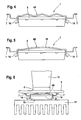
- the power semiconductor module 1 comprises a housing 9 preferably made of an epoxy compound and a carrier plate 5 made of an insulating ceramic substrate, wherein the carrier plate 5 forms the bottom of the housing 9.
- the housing 9 can also be made of metal.
- the support plate 5 is both on its side facing the housing 9 and on its side facing away from the housing 9 or outside with a metal layer 5.2, 5.3 provided, wherein the former metal layer 5.2 is structured according to the interconnects of a circuit arrangement. On this structured metal layer 5.2, a power semiconductor device 6 is arranged and soldered to the bottom side with the same.
- the power semiconductor component 6 is preferably contacted by means of bonding wires 8 with conductor tracks of the structured metal layer 5.2, wherein the bonding wire 8 is soldered in each case to the power semiconductor component 6 and the conductor track.
- Two preferably lug-shaped power terminals 7 form the electrical connections of the power semiconductor module 1, which are soldered at their ends within the housing 9 in each case with a conductor track of the circuit arrangement and each extending through the housing 9 preferably laterally outwardly.
- the two outer ends of the power terminals 7 are as terminals of a surface mounted component or component SMD (S urface- M ounted D evice) formed with solderable pads.
- SMD surface mounted component
- the electrical connections 7 of the power semiconductor module 1 need not be formed as SMD components. Rather, they can be screwed or plugged into the printed circuit board 3, on which the power semiconductor module is placed.
- the power terminals 7 are formed such that the terminals 7 inside the housing 9 extend first substantially vertically away from the carrier plate 5, then laterally through the housing 9 to the outside and then substantially perpendicular to the circuit board 3.
- the housing 9 has on a side facing away from the support plate 5 two spaced-apart cushion 4 made of an elastically and / or plastically deformable material, which serves to support the circuit board 3 when pressing the housing 9 against the heat sink 11 by means of a pressing element 12.
- two recesses may be provided, in where the two pillows are sitting.
- the two pillows 4 are each provided on the module side with an adhesive layer and glued to the outside of the housing 9. In this case, the pads 4 can already be glued in the manufacture of the power semiconductor module 1 with the housing, which simplifies the assembly of such an arrangement.
- the power semiconductor module 1 according to the invention is soldered to the printed conductors 3a of a printed circuit board 3 in such a way that the two pads 4 are arranged between the housing 9 of the power semiconductor module 1 and the printed circuit board 3.
- the pressing element 12 which is arranged on a side facing away from the power semiconductor module 1 side of the circuit board 3, presses the circuit board 3 against the two pads 4 and thus the power semiconductor module 1 against a heat sink 11, wherein the outside of the support plate 5 abuts the heat sink 11.
- thermal paste at contributes between the metallic outside of the support plate 5 and the heat sink 11 thermal paste at.
- the two pads 4 absorb the forces exerted by the contact pressure element 12 on the housing 9 of the power half-module 1 and thus relieve the electrical connections 7 of the power semiconductor module 1.
- the pads 4 ensure compliance with the required for the electrical operation isolation distances for creepage distances between the electrical connections 7 and the circuit board 3 safely.
- the cushions 4, together with the power terminals 7, compensate for temperature-induced deformations of the power semiconductor module 1, which are due to the different thermal expansion coefficients of the materials contained in the power semiconductor module 1.
- an additional cushion 4 ' may be arranged made of an elastic and / or plastic material, which can compensate for a component tolerances caused by distance between the circuit board 3 and the pressing member 12, so as to ensure that the pressing member 12 exerts a sufficiently large force on the circuit board 3.
- an additional cushion between the contact pressure element and the printed circuit board is generally not required in the case of the component tolerances that are available in practice.
- Fig. 3 shows an alternative embodiment of the arrangement according to the invention, in which the pressing member 12 is integrally formed with a first housing part 13.2, which forms the lid of a housing 13 made of metal, preferably for example cast iron, whereas the heat sink 11 integral with a second housing part 13.1 of the housing 13 is formed.
- the two housing parts 13.1, 13.2 enclose the printed circuit board 3 together with the electronic components 1, 2 attached to the printed circuit board.
- a separate pressing element 12 is provided for each cushion 4.
- Fig. 4 shows an alternative embodiment of the power semiconductor module according to the invention, wherein for the corresponding components, the same reference numerals are used as in the previous figures again.
- This embodiment is different from the embodiment of FIG Fig. 1 in that, instead of a cushion, a spring element 4A is provided.
- the spring element 4A is a thin plate made of spring steel, which is shaped like a zigzag and laterally bent at its edges.
- the two laterally bent edges of the spring element form brackets 14 which laterally surround the housing of the power semiconductor module and secure the spring element to the housing.
- the thin plate of spring steel is deformed so that the plate can be compressed when a contact force is exerted on the plate from above. Since the two brackets 14 are slightly bent inwardly, a sufficient clamping voltage is achieved even when the spring element is pressed against the housing.
- Fig. 5 shows an alternative embodiment, which differs from the embodiment of Fig. 4 distinguished by the spring element.
- the spring element 4B of Fig. 5 is a thin plate made of spring steel, which is bent at its edges. Between the two edges, the brackets 14 again for attaching the spring element serve on the housing, the thin plate is curved outward. As a result, an outwardly curved bearing surface 15 is created for the circuit board, which yields under pressure.
- the spring elements 4A, 4B of 4 or FIG. 5 can also be made inexpensively from a flexible elastically deformable plastic, for example as an injection molded part in large quantities. They may have a zigzag-shaped or an outwardly curved region or else a plurality of sections each with a zigzag-shaped or outwardly curved region.
- Fig. 6 shows the arrangement according to the invention, the power semiconductor module 1 of Fig. 5 and the printed circuit board 3, wherein the spring element 4B is arranged between the printed circuit board and the housing 9 of the power semiconductor module 1.
- the circuit board 3 is supported on the outwardly curved contact surface 15 of the spring element 4B.
- the arrangement can also the power semiconductor module of Fig. 4 exhibit.
Abstract
Description
Die Erfindung betrifft eine Anordnung aus mindestens einem Leistungshalbleitermodul und einer Leiterplatte sowie ein Leistungshalbleitermodul.The invention relates to an arrangement of at least one power semiconductor module and a printed circuit board and a power semiconductor module.
Eine derartige Anordnung findet sich in verschiedenen Gebieten der Elektrotechnik, beispielsweise in einer Antriebssteuereinrichtung für einen Elektromotor. Die Schaltungsanordnung einer solchen Antriebssteuereinrichtung besteht aus verschiedenen Funktionsblöcken, beispielsweise Gleichrichtern, Wechselrichtern und Bremsstellern. Diese Funktionsblöcke werden durch Leistungshalbleiterbauteile und/oder Leistungshalbleitermodule gebildet, wobei letztere alle notwendigen Leistungshalbleiter und darüber hinaus weitere Komponenten enthalten können, beispielsweise Komponenten zur Überwachung der Leistungshalbleiter, die beispielsweise Temperatur- und / oder Stromsensoren aufweisen können. Die Leistungshalbleiterbauteile und/oder Leistungshalbleitermodule werden üblicherweise auf einer Leiterplatte angeordnet und durch Schrauben, Stecken oder Löten mit derselben verbunden.Such an arrangement can be found in various fields of electrical engineering, for example in a drive control device for an electric motor. The circuit arrangement of such a drive control device consists of various function blocks, such as rectifiers, inverters and brake actuators. These functional blocks are formed by power semiconductor components and / or power semiconductor modules, with the latter being able to contain all the necessary power semiconductors and, in addition, further components, for example components for monitoring the power semiconductors, which may have, for example, temperature and / or current sensors. The power semiconductor components and / or power semiconductor modules are usually arranged on a printed circuit board and connected by screwing, plugging or soldering with the same.
Aus der
Dieser bekannte Aufbau von Leistungshalbleiterbauteilen und/oder Leistungshalbleitermodulen einschließlich Schutzeinrichtungen und Ansteuerelektronik erfordert einen hohen Materialaufwand und in der Fertigung zahlreiche Zwischenschritte sowie Schraub-, Löt- und Montageschritte. Weiterhin ist die durch die Verlustleistung beim Betrieb der Leistungshalbleitermodule verursachte Wärmeentwicklung im Regelfall auf relativ kleinen Flächen konzentriert. Diese Wärmeentwicklung kann die Leistung des Gesamtsystems und die Zuverlässigkeit der Leistungshalbleitermodule verringern. Daher bedarf es eines größeren Aufwandes zur Kühlung dieser Leistungshalbleitermodule.This known structure of power semiconductor components and / or power semiconductor modules including protective devices and control electronics requires a high cost of materials and numerous intermediate steps in manufacturing and screwing, soldering and assembly steps. Furthermore, the heat generated by the power loss during operation of the power semiconductor modules is usually concentrated on relatively small areas. This heat development can reduce the performance of the overall system and the reliability of the power semiconductor modules. Therefore, it requires a greater effort to cool these power semiconductor modules.
Alternativ kommen in entsprechenden Aufbauten beispielsweise sogenannte diskrete Leistungshalbleiterbauteile zum Einsatz. Diese stellen in der Regel Einzelfunktionen in jeweils einem Gehäuse dar. Dabei sind Leistungshalbleiter direkt auf eine metallische Trägerplatte gelötet und zum Schutz umhüllt. Diese Bauteile können in der leistungselektronischen Anordnung räumlich verteilt werden, sodass eine bessere Verteilung der Wärme im Kühlkörper erzielt wird und gegebenenfalls der Aufwand zur Umsetzung einer angemessenen Kühlung reduziert werden kann. Sie zeichnen sich durch ein mechanisch robustes Design aus und sind als Elemente für verschiedenste Schaltungsfunktionen in standardisierten Bauformen durch hohe Stückzahlen kostengünstig verfügbar. Nachteilig ist, dass die Trägerplatte, welche der Wärmeabfuhr dient, vom Leistungshalbleiter nicht elektrisch isoliert ist und mithin ein elektrisches Potential führt. Bei der Montage von derartigen diskreten Leistungshalbleiterbauteilen auf einem gemeinsamen Kühlkörper ist daher eine zusätzliche Isolierung notwendig, die jedoch die Wärmeableitung an den Kühlkörper deutlich nachteilig beeinflusst. In der Regel werden diese Bauteile durch Schraub- oder Klemmmontage auf dem Kühlkörper befestigt, dies erfordert zusätzliche Montageteile, etwa Isolierplättchen und/oder Wärmeleitmaterialien, Schrauben, Montageklammern und einen entsprechenden Montageaufwand. Weiterhin muss man in der Regel Einschränkungen im Hinblick auf den Lötprozess in Kauf nehmen. Wegen der fehlenden Isolation werden Bauteile verwendet, die in ihren Abmessungen und anderen Eigenschaften zu den beschriebenen Bauteilen vergleichbar sind, bei denen jedoch keine massive metallische Trägerplatte zum Einsatz kommt, sondern eine beidseitig metallisierte keramische Grundplatte Verwendung findet. Solche Bauteile sind beispielsweise in der
Die Anschlusskämme von Bauteilen, die der elektrischen Kontaktierung dienen, werden in der Regel flach nach den Seiten herausgeführt. Damit besteht für viele Anwendungen das Problem der Einhaltung von Luft- und Kriechstrecken zwischen den Anschlüssen mit verschiedenen Spannungspotentialen einerseits und zwischen den Anschlüssen und der metallisierten Trägerplatte bzw. dem Kühlkörper in der Anwendung andererseits.The connecting combs of components that serve the electrical contact, are usually led out flat to the sides. Thus, for many applications there is the problem of maintaining clearances and creepage distances between the terminals with different voltage potentials on the one hand and between the terminals and the metallized carrier plate or the heat sink in the application on the other.
Die
Aus der
Der Erfindung liegt daher die Aufgabe zugrunde, eine Anordnung eines Leistungshalbleitermoduls und einer Leiterplatte mit verbesserten technischen Eigenschaften bereitzustellen.The invention is therefore based on the object to provide an arrangement of a power semiconductor module and a printed circuit board with improved technical properties.
Der Erfindung liegt auch die Aufgabe zugrunde, eine kostengünstigere, kompaktere Anordnung eines Leistungshalbleitermoduls und einer Leiterplatte bereitzustellen, die einen kleineren Montageaufwand erfordert.The invention is also based on the object to provide a lower-cost, more compact arrangement of a power semiconductor module and a printed circuit board, which requires a smaller installation effort.
Außerdem liegt der Erfindung die Aufgabe zugrunde, ein Leistungshalbleitermodul für eine derartige Anordnung bereitzustellen.In addition, the invention has for its object to provide a power semiconductor module for such an arrangement.
Diese Aufgaben werden erfindungsgemäß durch die in den Patentansprüchen 1 und 11 angegebenen Merkmale gelöst. Bevorzugte Ausführungsformen der Erfindung sind Gegenstand der Unteransprüche.These objects are achieved by the features specified in the
Die erfindungsgemäße Anordnung umfasst mindestens ein Leistungshalbleitermodul und eine Leiterplatte mit Leiterbahnen, wobei das Leistungshalbleitermodul ein Gehäuse mit Leistungsanschlüssen aufweist, die sich durch das Gehäuse nach außen erstrecken und mit den Leiterbahnen der Leiterplatte kontaktiert sind.The inventive arrangement comprises at least one power semiconductor module and a printed circuit board with conductor tracks, wherein the power semiconductor module has a housing with power terminals, which extend through the housing to the outside and are contacted with the conductor tracks of the printed circuit board.
Die erfindungsgemäße Anordnung zeichnet sich dadurch aus, dass zwischen dem Gehäuse des Leistungshalbleitermoduls und der Leiterplatte elastisch oder plastisch verformbare Mittel angeordnet sind, über die eine Anpresskraft von der Leiterplatte auf das Gehäuse übertragbar ist. Dadurch werden die Leistungsanschlüsse des Leistungshalbleitermoduls entlastet. Es besteht somit nicht die Gefahr des Verbiegens der Anschlusselemente. Darüber hinaus wird sichergestellt, dass ein vorgegebener Abstand zwischen den Anschlusselementen und der Metallisierung der Leiterplatte eingehalten wird. Von Vorteil ist, wenn die elastisch oder plastisch verformbaren Mittel aus einem wärmeleitenden Material bestehen.The arrangement according to the invention is characterized in that elastically or plastically deformable means are arranged between the housing of the power semiconductor module and the printed circuit board, via which means a contact pressure force can be transmitted from the printed circuit board to the housing. As a result, the power terminals of the power semiconductor module are relieved. There is thus no risk of bending the connection elements. In addition, it is ensured that a predetermined distance between the connection elements and the metallization of the circuit board is maintained. It is advantageous if the elastically or plastically deformable means consist of a thermally conductive material.
Darüber hinaus umfasst die Anordnung mindestens ein Anpresselement, das an der dem Leistungshalbleitermodul abgewandten Seite der Leiterplatte angeordnet ist, und mindestens einen Kühlkörper, der an der Seite des Leistungshalbleitermoduls angeordnet ist, die der Leiterplatte abgewandt ist. Das Anpresselement ist einstückig mit einem ersten Gehäuseteil eines Gehäuses ausgebildet, während der Kühlkörper einstückig mit einem zweiten Gehäuseteil des Gehäuses ausgebildet ist. Dabei umschließen die beiden Gehäuseteile die Leiterplatte zusammen mit den an der Leiterplatte angebrachten elektronischen Bauteilen.In addition, the arrangement comprises at least one pressing element, which is arranged on the side facing away from the power semiconductor module side of the printed circuit board, and at least one heat sink, on the side of the power semiconductor module is arranged, which faces away from the circuit board. The pressing element is formed integrally with a first housing part of a housing, while the cooling body is formed integrally with a second housing part of the housing. The two housing parts enclose the printed circuit board together with the electronic components attached to the printed circuit board.
Unter elastisch oder plastisch verformbaren Mitteln werden alle Mittel verstanden, mit denen die Leistungsanschlüsse entlastet werden, wenn auf die Leiterplatte der erfindungsgemäßen Anordnung eine Anpresskraft ausgeübt wird. Vorzugsweise sind die Mittel elastisch verformbar, so dass sie eine Rückstellkraft ausüben können. Es ist aber grundsätzlich auch möglich, dass die Mittel plastisch verformbar sind, so dass sich die Leiterplatte an den plastisch verformbaren Mitteln, nicht aber den Anschlusselementen abstützt.Elastic or plastically deformable means are understood to be all means with which the power connections are relieved when a contact pressure force is exerted on the printed circuit board of the arrangement according to the invention. Preferably, the means are elastically deformable so that they can exert a restoring force. But it is also possible in principle that the means are plastically deformable, so that the circuit board is supported on the plastically deformable means, but not the connection elements.
Bei einer bevorzugten Ausführungsform der Erfindung sind die elastisch oder plastisch verformbaren Mittel als mindestens ein Federelement ausgebildet, das derart verformt ist, dass das Federelement mindestens eine nach außen gewölbte Fläche zur Anlage der Leiterplatte aufweist, wobei die Anlagefläche unter Druck federnd nachgibt. Dabei ist das Federelement vorzugsweise klemmend auf das Gehäuse des Leitungshalbleitermoduls aufgesetzt ist. Hierzu kann das Federelement das Gehäuse seitlich übergreifende Klammern aufweisen. Das Federelement besteht vorzugsweise aus Metall, beispielsweise einem Federstahl.In a preferred embodiment of the invention, the elastically or plastically deformable means are formed as at least one spring element which is deformed such that the spring element has at least one outwardly curved surface for abutment of the printed circuit board, wherein the contact surface yields resiliently under pressure. In this case, the spring element is preferably placed by clamping on the housing of the line semiconductor module. For this purpose, the spring element may have the housing laterally overlapping brackets. The spring element is preferably made of metal, for example a spring steel.
Das Federelement kann beispielsweise eine nach außen gebogene Metallklammer sein.The spring element may for example be an outwardly bent metal clip.
Eine alternative Ausführungsform sieht vor, dass die elastisch oder plastisch verformbaren Mittel als mindestens ein elastisch oder plastisch verformbares Kissen zwischen Leistungshalbleitermodul und einer Leiterplatte ausgebildet sind. Das elastisch oder plastisch verformbare Kissen kann auf der Oberfläche des Gehäuses des Leistungshalbleitermoduls befestigt sein oder in eine Ausnehmung oder Vertiefung des Gehäuses eingesetzt sein. Vorzugsweise ist das Kissen mit dem Gehäuse des Leistungshalbleitermoduls verklebt. Das Kissen kann aber auch dadurch gebildet werden, dass die Anordnung des Leistungshalbleitermoduls nach dem Verlöten mit einer Leiterplatte mittels einer elastisch verformbaren und elektrisch isolierenden Masse, beispielsweise Silikonkautschuk, vergossen wird.An alternative embodiment provides that the elastically or plastically deformable means are formed as at least one elastically or plastically deformable cushion between the power semiconductor module and a printed circuit board. The elastically or plastically deformable pad may be fixed to the surface of the housing of the power semiconductor module or inserted into a recess or depression of the housing. Preferably, the pad is glued to the housing of the power semiconductor module. The pillow can also be characterized be formed, that the arrangement of the power semiconductor module after soldering with a circuit board by means of an elastically deformable and electrically insulating material, such as silicone rubber, is cast.
Das elastisch oder plastisch verformbare Kissen kann aus unterschiedlichen Materialien bestehen, die plastische und/oder elastische und vorzugsweise elektrisch isolierende Eigenschaften haben. Entscheidend ist, dass das Kissen die vom Anpresselement auf das Gehäuse des Leistungshalbteilermoduls ausgeübte Kraft aufnimmt und somit das Gehäuse an eine Kühlplatte zur verbesserten thermischen Ankopplung dauerhaft andrückt. Dabei werden auch die elektrischen Anschlusselemente des Leistungshalbleitermoduls entlastet. Zudem stellt das elektrisch isolierende Kissen die Einhaltung der für den elektrischen Betrieb geforderten Isolationsabstände für Luft- bzw. Kriechstrecken zwischen den elektrischen Anschlüssen und der Leiterplatte sicher. Außerdem kann das Kissen zusammen mit den Leistungsanschlüssen temperaturbedingte Verformungen des Leistungshalbleitermoduls ausgleichen, die auf die verschiedenen thermischen Ausdehnungskoeffizienten der im Leistungshalbleitermodul enthaltenen Materialien zurückzuführen sind.The elastically or plastically deformable cushion may consist of different materials which have plastic and / or elastic and preferably electrically insulating properties. It is crucial that the pad absorbs the force exerted by the contact pressure element on the housing of the power half-submodule and thus permanently presses the housing onto a cooling plate for improved thermal coupling. In this case, the electrical connection elements of the power semiconductor module are relieved. In addition, the electrically insulating cushion ensures compliance with the insulation distances required for electrical operation for creepage distances between the electrical connections and the printed circuit board. In addition, the pad together with the power terminals can compensate for temperature-induced deformations of the power semiconductor module, which are due to the different thermal expansion coefficients of the materials contained in the power semiconductor module.
Das mindestens eine Leistungshalbleitermodul umfasst vorzugsweise eine Trägerplatte aus isolierendem Keramiksubstrat, die den Boden des Gehäuses bildet. Die Trägerplatte ist auf einer Seite mit einer entsprechend einer Schaltungsanordnung des Leistungshalbleitermoduls strukturierten Metallschicht und auf der dieser Seite gegenüberliegenden Seite bzw. Außenseite mit einer durchgehenden Metallschicht versehen, die der thermischen Anbindung des Leistungshalbleitermoduls an einen Kühlkörper dient. Auf der strukturierten Metallschicht ist mindestens ein Leistungshalbleiterbauteil angeordnet und unterseitig mit derselben verlötet sowie oberseitig mittels elektrischer Verbindungselemente, die vorzugsweise als Bonddrähte ausgebildet sind, mit derselben kontaktiert.The at least one power semiconductor module preferably comprises a carrier plate of insulating ceramic substrate, which forms the bottom of the housing. The carrier plate is provided on one side with a metal layer structured in accordance with a circuit arrangement of the power semiconductor module and on the side or outside opposite this side with a continuous metal layer which serves to thermally connect the power semiconductor module to a heat sink. At least one power semiconductor component is arranged on the structured metal layer and is soldered to the same on the underside and also contacted with the upper side by means of electrical connecting elements, which are preferably designed as bonding wires.
Auf der Seite der Leiterplatte, die dem Leistungshalbleitermodul abgewandt ist, können zwischen dem Anpresselement und der Leiterplatte ebenfalls elastisch oder plastisch verformbare Mittel angeordnet sein, um einen durch Bauteiltoleranzen bedingten Abstand zwischen der Leiterplatte und dem Anpresselement auszugleichen. Dadurch wird unabhängig von Bauteiltoleranzen sichergestellt, dass das Anpresselement eine genügend große Kraft auf die Leiterplatte ausübt.On the side of the printed circuit board, which faces away from the power semiconductor module, elastically or plastically deformable means can also be arranged between the pressing element and the printed circuit board in order to achieve a component tolerance to compensate for the conditional distance between the printed circuit board and the pressing element. This ensures regardless of component tolerances that the contact element exerts a sufficiently large force on the circuit board.
Im Folgenden werden Ausführungsbeispiele der Erfindung unter Bezugnahme auf die Figuren näher erläutert. Es zeigen:
- Fig. 1
- eine erste Ausführungsform des erfindungsgemäßen Leistungshalbleitermoduls,
- Fig. 2
- eine erfindungsgemäße Anordnung aus dem Leistungshalbleitermodul von
Fig. 1 und einer Leiterplatte, und - Fig. 3
- eine alternative Ausführungsform der erfindungsgemäßen Anordnung mit dem erfindungsgemäßen Leistungshalbleitermodul von
Fig. 1 , - Fig. 4
- eine zweite Ausführungsform des erfindungsgemäßen Leistungshalbleitermoduls,
- Fig. 5
- eine weitere Ausführungsform des erfindungsgemäßen Leistungshalbleitermoduls und
- Fig. 6
- eine erfindungsgemäße Anordnung aus dem Leistungshalbleitermodul von
Fig. 5 und einer Leiterplatte.
- Fig. 1
- a first embodiment of the power semiconductor module according to the invention,
- Fig. 2
- an inventive arrangement of the power semiconductor module of
Fig. 1 and a circuit board, and - Fig. 3
- an alternative embodiment of the inventive arrangement with the power semiconductor module according to the invention of
Fig. 1 . - Fig. 4
- A second embodiment of the power semiconductor module according to the invention,
- Fig. 5
- a further embodiment of the power semiconductor module according to the invention and
- Fig. 6
- an inventive arrangement of the power semiconductor module of
Fig. 5 and a circuit board.
Das erfindungsgemäße Leistungshalbleitermodul 1 umfasst ein vorzugsweise aus einer Epoxidmasse gefertigtes Gehäuse 9 und eine Trägerplatte 5 aus einem isolierenden Keramiksubstrat, wobei die Trägerplatte 5 den Boden des Gehäuses 9 bildet. Grundsätzlich kann das Gehäuse 9 auch aus Metall gefertigt sein. Die Trägerplatte 5 ist sowohl auf ihrer dem Gehäuse 9 zugewandten Seite als auch auf ihrer dem Gehäuse 9 abgewandten Seite bzw. Außenseite mit einer Metallschicht 5.2, 5.3 versehen, wobei die erstere Metallschicht 5.2 entsprechend der Leiterbahnen einer Schaltungsanordnung strukturiert ist. Auf dieser strukturierten Metallschicht 5.2 ist ein Leistungshalbleiterbauteil 6 angeordnet und unterseitig mit derselben verlötet. Oberseitig ist das Leistungshalbleiterbauteil 6 vorzugsweise mittels Bonddrähten 8 mit Leiterbahnen der strukturierten Metallschicht 5.2 kontaktiert, wobei der Bonddraht 8 jeweils mit dem Leistungshalbleiterbauteil 6 und der Leiterbahn verlötet ist. Zwei vorzugsweise laschenförmig ausgebildete Leistungsanschlüsse 7 bilden die elektrischen Anschlüsse des Leistungshalbleitermoduls 1, die an ihren Enden innerhalb des Gehäuses 9 jeweils mit einer Leiterbahn der Schaltungsanordnung verlötet sind und sich jeweils durch das Gehäuse 9 vorzugsweise seitlich nach außen erstrecken. Die beiden äußeren Enden der Leistungsanschlüsse 7 sind als Anschlüsse eines oberflächenmontierten Bauteils bzw. SMD Bauteils (Surface-Mounted Device) mit lötfähigen Anschlussflächen ausgebildet. Grundsätzlich müssen die elektrischen Anschlüsse 7 des Leistungshalbleitermoduls 1 nicht als SMD Bauteile ausgebildet sein. Vielmehr können diese mit der Leiterplatte 3, auf der das Leistungshalbleitermodul aufgesetzt wird, verschraubt oder in diese gesteckt sein.The
Zur Einhaltung der für den elektrischen Betrieb geforderten Isolationsabstände für Luft- und Kriechstrecken zwischen den innerhalb des Gehäuses 9 liegenden Abschnitten der elektrischen Anschlüsse 7 und der Trägerplatte 5 und zwischen den außerhalb des Gehäuses 9 liegenden Abschnitten der elektrischen Anschlüssen 7 und der Leiterplatte 3 sowie einem Kühlkörper 11, sind die Leistungsanschlüsse 7 derart ausgebildet, dass sich die Anschlüsse 7 innerhalb des Gehäuses 9 zuerst im Wesentlichen senkrecht von der Trägerplatte 5 weg, dann seitlich durch das Gehäuses 9 nach außen und dann im Wesentlichen senkrecht zur Leiterplatte 3 erstrecken.To comply with the required for the electrical operation isolation distances for creepage distances and between the lying within the
Das Gehäuse 9 weist an einer der Trägerplatte 5 abgewandten Außenseite zwei im Abstand zueinander angeordnete Kissen 4 aus einem elastisch und/oder plastisch verformbaren Material auf, das der Abstützung der Leiterplatte 3 beim Anpressen des Gehäuses 9 gegen den Kühlkörper 11 mittels eines Anpresselements 12 dient. An der Außenseite des Gehäuses 9 können zwei Vertiefungen vorgesehen sein, in denen die beiden Kissen sitzen. Die beiden Kissen 4 sind jeweils modulseitig mit einer Klebschicht versehen und mit der Außenseite des Gehäuses 9 verklebt. Dabei können die Kissen 4 bereits bei der Fertigung des Leistungshalbleitermoduls 1 mit dessen Gehäuse verklebt werden, was die Montage einer derartigen Anordnung vereinfacht.The
Bei dem Ausführungsbeispiel von
Die beiden Kissen 4 nehmen die von dem Anpresselement 12 auf das Gehäuse 9 des Leistungshalbteilermoduls 1 ausgeübten Kräfte auf und entlasten somit die elektrischen Anschlüsse 7 des Leistungshalbleitermoduls 1. Dadurch wird die Verformung der elektrischen Anschlüsse 7 verhindert, so dass das Leistungshalbleitermodul 1 von der Leiterplatte 3 beabstandet bleibt. Folglich stellen die Kissen 4 die Einhaltung der für den elektrischen Betrieb geforderten Isolationsabstände für Luft- bzw. Kriechstrecken zwischen den elektrischen Anschlüssen 7 und der Leiterplatte 3 sicher. Außerdem gleichen die Kissen 4 zusammen mit den Leistungsanschlüssen 7 temperaturbedingte Verformungen des Leistungshalbleitermoduls 1 aus, die auf die verschiedenen thermischen Ausdehnungskoeffizienten der im Leistungshalbleitermodul 1 enthaltenen Materialien zurückzuführen sind.The two
Zwischen dem Anpresselement 12 und der Leiterplatte kann ein zusätzliches Kissen 4' aus einem elastischen und/oder plastischen Material angeordnet sein, das einen durch Bauteiltoleranzen bedingten Abstand zwischen der Leiterplatte 3 und dem Anpresselement 12 ausgleichen kann, so dass sichergestellt ist, dass das Anpresselement 12 eine genügend große Kraft auf die Leiterplatte 3 ausübt. Ein zusätzliches Kissen zwischen Anpresselement und Leiterplatte ist aber bei den in der Praxis vorliegenden Bauteiltoleranzen im Allgemeinen nicht erforderlich.Between the pressing
Die Federelemente 4A, 4B von
Claims (16)
einer Leiterplatte (3) mit Leiterbahnen,
mindestens einem Leistungshalbleitermodul (1), das ein Gehäuse (9) mit Leistungsanschlüssen (7) aufweist, die sich durch das Gehäuse (9) nach außen erstrecken und mit den Leiterbahnen (3a) der Leiterplatte (3) kontaktiert sind,
und
mindestens einem Kühlkörper (11), der an der Seite des Leistungshalbleitermoduls angeordnet ist, die der Leiterplatte abgewandt ist,
wobei zwischen dem Gehäuse (9) des Leistungshalbleitermoduls (1) und der Leiterplatte (3) elastisch oder plastisch verformbare Mittel (4) angeordnet sind, über die eine Anpresskraft von der Leiterplatte auf das Gehäuse unter Entlastung der Leistungsanschlüsse (7) übertragbar ist,
dadurch gekennzeichnet, dass
die Anordnung mindestens ein Anpresselement (12) umfasst, das an der dem Leistungshalbleitermodul (1) abgewandten Seite der Leiterplatte (3) angeordnet ist, wobei das Anpresselement (12) einstückig mit einem ersten Gehäuseteil (13.2) eines Gehäuses (13) und der Kühlkörper (11) einstückig mit einem zweiten Gehäuseteil (13.1) des Gehäuses (13) ausgebildet sind, wobei die beiden Gehäuseteile die Leiterplatte (3) umschließen.Arrangement with
a printed circuit board (3) with conductor tracks,
at least one power semiconductor module (1) having a housing (9) with power terminals (7) which extend through the housing (9) to the outside and with the printed conductors (3a) of the printed circuit board (3) are contacted,
and
at least one heat sink (11), which is arranged on the side of the power semiconductor module, which faces away from the printed circuit board,
between the housing (9) of the power semiconductor module (1) and the printed circuit board (3) elastically or plastically deformable means (4) are arranged, via which a contact pressure of the circuit board to the housing with discharge of the power terminals (7) is transferable,
characterized in that
the arrangement comprises at least one pressing element (12) which is arranged on the side facing away from the power semiconductor module (1) side of the printed circuit board (3), wherein the pressing element (12) integral with a first housing part (13.2) of a housing (13) and the heat sink (11) are integrally formed with a second housing part (13.1) of the housing (13), wherein the two housing parts enclose the circuit board (3).
dadurch gekennzeichnet,
dass die elastisch oder plastisch verformbaren Mittel (4) als mindestens ein Federelement (4A, 4B) ausgebildet sind, das derart verformt ist, das das Federelement mindestens eine nach außen gewölbte Fläche (15) zur Anlage einer Leiterplatte aufweist, wobei die Anlagefläche unter Druck federnd nachgibt, und
dass das Federelement (4A, 4B) klemmend auf das Gehäuse (9) des Leitungshalbleitermoduls (1) aufgesetzt ist.Power semiconductor module having a housing (9) having power terminals (7) which extend through the housing (9) to the outside and can be contacted with the conductor tracks of a printed circuit board, wherein on the side of the housing (9) of the power semiconductor module (1), which is facing during assembly of the power semiconductor module of the circuit board, elastically or plastically deformable means (4) are arranged, via which a contact pressure of the circuit board on the housing under discharge of the power terminals (7) is transferable,
characterized,
in that the elastically or plastically deformable means (4) are designed as at least one spring element (4A, 4B) which is deformed in such a way that the spring element has at least one outwardly curved surface (15) for contacting a printed circuit board, wherein the contact surface is under pressure yielding resiliently, and
is that the spring element (4A, 4B) by clamping on the housing (9) of the power semiconductor module (1) is placed.
Applications Claiming Priority (1)
| Application Number | Priority Date | Filing Date | Title |
|---|---|---|---|
| DE102007014789A DE102007014789B3 (en) | 2007-03-28 | 2007-03-28 | Arrangement of at least one power semiconductor module and a printed circuit board and power semiconductor module |
Publications (3)
| Publication Number | Publication Date |
|---|---|
| EP1976358A2 true EP1976358A2 (en) | 2008-10-01 |
| EP1976358A3 EP1976358A3 (en) | 2010-07-07 |
| EP1976358B1 EP1976358B1 (en) | 2013-04-24 |
Family
ID=39561858
Family Applications (1)
| Application Number | Title | Priority Date | Filing Date |
|---|---|---|---|
| EP08004261.7A Active EP1976358B1 (en) | 2007-03-28 | 2008-03-07 | Assembly of at least one voltage semiconductor module and a conductor board |
Country Status (4)
| Country | Link |
|---|---|
| US (1) | US7780469B2 (en) |
| EP (1) | EP1976358B1 (en) |
| JP (1) | JP5108586B2 (en) |
| DE (1) | DE102007014789B3 (en) |
Cited By (5)
| Publication number | Priority date | Publication date | Assignee | Title |
|---|---|---|---|---|
| WO2010044011A1 (en) * | 2008-10-14 | 2010-04-22 | Koninklijke Philips Electronics N.V. | A system for heat conduction between two connectable members |
| DE102009047703A1 (en) * | 2009-12-09 | 2011-06-16 | Robert Bosch Gmbh | Electronic circuit for use in automotive area, has heat producing component exhibiting housing side that is connected with printed circuit board by attachment element, which separates housing side regarding heat transfer from circuit board |
| EP2525397A1 (en) | 2011-05-17 | 2012-11-21 | IXYS Semiconductor GmbH | Power semiconductor |
| DE202014003171U1 (en) | 2014-04-15 | 2014-05-14 | Ixys Semiconductor Gmbh | The power semiconductor module |
| EP2933836A1 (en) | 2014-04-15 | 2015-10-21 | IXYS Semiconductor GmbH | Power semiconductor module |
Families Citing this family (18)
| Publication number | Priority date | Publication date | Assignee | Title |
|---|---|---|---|---|
| JP4789997B2 (en) * | 2008-11-20 | 2011-10-12 | 三菱電機株式会社 | Electronic board device |
| JP4983824B2 (en) * | 2009-02-25 | 2012-07-25 | ブラザー工業株式会社 | Heat sink holding member and liquid discharge device |
| US20110279980A1 (en) * | 2010-05-11 | 2011-11-17 | Silicon Integrated Systems Corp. | Heat dissipation structure for liquid crystal television |
| JP5529208B2 (en) * | 2011-08-25 | 2014-06-25 | トヨタ自動車株式会社 | Power module structure and molding method |
| KR101228841B1 (en) | 2011-10-04 | 2013-02-04 | 엘에스산전 주식회사 | A springy clip type apparatus for fastening power semiconductor |
| KR200472484Y1 (en) * | 2012-06-14 | 2014-05-02 | 엘에스산전 주식회사 | Device for fixing power semiconductor |
| JP5686127B2 (en) * | 2012-11-16 | 2015-03-18 | 日立金属株式会社 | Signal transmission device |
| US9147630B2 (en) * | 2013-03-05 | 2015-09-29 | Infineon Technologies Ag | Power semiconductor assembly and module |
| DE102015200548A1 (en) * | 2015-01-15 | 2016-07-21 | Zf Friedrichshafen Ag | Arrangement for the dissipation of at least one electronic component |
| US9913361B2 (en) | 2016-01-06 | 2018-03-06 | International Business Machines Corporation | Integrated circuit device assembly |
| US10021803B2 (en) * | 2016-02-26 | 2018-07-10 | Delta Electronics, Inc. | Power supply |
| JP6645315B2 (en) * | 2016-03-29 | 2020-02-14 | アイシン・エィ・ダブリュ株式会社 | Inverter device and method of manufacturing inverter device |
| KR101841836B1 (en) * | 2016-07-05 | 2018-03-26 | 김구용 | PCB module having multi-directional heat-radiation structure, and radiation plate, multi-layer PCB assembly, and module case used in the same PCB module |
| DE202019101524U1 (en) | 2019-03-18 | 2019-04-29 | Andreas Groch | System for installing a solar module |
| DE102019206523A1 (en) | 2019-05-07 | 2020-11-12 | Zf Friedrichshafen Ag | Power module with housed power semiconductors for controllable electrical power supply to a consumer |
| CN111987523A (en) * | 2019-05-24 | 2020-11-24 | 泰科电子(上海)有限公司 | Connector and radiator |
| DE102020206145A1 (en) | 2020-05-15 | 2021-11-18 | Zf Friedrichshafen Ag | Method for producing a power module, power module, electrical device and motor vehicle |
| DE102021129117A1 (en) | 2021-11-09 | 2023-05-11 | Rolls-Royce Deutschland Ltd & Co Kg | circuit board arrangement |
Citations (6)
| Publication number | Priority date | Publication date | Assignee | Title |
|---|---|---|---|---|
| EP0513410B1 (en) | 1991-05-15 | 1993-12-15 | IXYS Semiconductor GmbH | Semiconductor power module and method of making such a module |
| WO1994029901A1 (en) | 1993-06-07 | 1994-12-22 | Melcher Ag | Securing device for semiconductor circuit components |
| US6035523A (en) | 1995-06-16 | 2000-03-14 | Apple Computer, Inc. | Method and apparatus for supporting a component on a substrate |
| DE19646396C2 (en) | 1996-11-11 | 2001-06-28 | Semikron Elektronik Gmbh | Power semiconductor module for different circuit variants |
| US6404065B1 (en) | 1998-07-31 | 2002-06-11 | I-Xys Corporation | Electrically isolated power semiconductor package |
| DE19625240B4 (en) | 1995-10-26 | 2004-04-08 | Mitsubishi Denki K.K. | Semiconductor device |
Family Cites Families (19)
| Publication number | Priority date | Publication date | Assignee | Title |
|---|---|---|---|---|
| ATE39788T1 (en) * | 1982-09-09 | 1989-01-15 | Siemens Ag | DEVICE FOR COOLING A NUMBER OF INTEGRATED COMPONENTS COMBINED TO FORM FLAT ASSEMBLIES. |
| US4750089A (en) * | 1985-11-22 | 1988-06-07 | Texas Instruments Incorporated | Circuit board with a chip carrier and mounting structure connected to the chip carrier |
| DE3604313A1 (en) * | 1986-02-12 | 1987-08-13 | Bbc Brown Boveri & Cie | Power semiconductor module |
| US5184211A (en) * | 1988-03-01 | 1993-02-02 | Digital Equipment Corporation | Apparatus for packaging and cooling integrated circuit chips |
| DE9112099U1 (en) * | 1991-09-27 | 1991-12-05 | Siemens Nixdorf Informationssysteme Ag, 4790 Paderborn, De | |
| US5396404A (en) * | 1993-09-20 | 1995-03-07 | Delco Electronics Corp. | Heat sinking assembly for electrical components |
| US5483103A (en) * | 1994-02-24 | 1996-01-09 | Harris Corporation | Means for clamping a semi-conductor to a support |
| US5504653A (en) * | 1994-11-21 | 1996-04-02 | Delco Electronics Corp. | Heat sinking assembly for electrical components |
| US5889652A (en) * | 1997-04-21 | 1999-03-30 | Intel Corporation | C4-GT stand off rigid flex interposer |
| US6180436B1 (en) * | 1998-05-04 | 2001-01-30 | Delco Electronics Corporation | Method for removing heat from a flip chip semiconductor device |
| US6566879B1 (en) * | 2000-02-29 | 2003-05-20 | Koninklijke Philips Electronics, N.V. | Apparatus for effecting heat transfer from power semiconductors |
| US6631078B2 (en) * | 2002-01-10 | 2003-10-07 | International Business Machines Corporation | Electronic package with thermally conductive standoff |
| US7023699B2 (en) * | 2002-06-10 | 2006-04-04 | Visteon Global Technologies, Inc. | Liquid cooled metal thermal stack for high-power dies |
| US6633485B1 (en) * | 2002-11-20 | 2003-10-14 | Illinois Tool Works Inc. | Snap-in heat sink for semiconductor mounting |
| EP1424728A1 (en) * | 2002-11-27 | 2004-06-02 | Abb Research Ltd. | Power semiconductor module |
| JP4453498B2 (en) * | 2004-09-22 | 2010-04-21 | 富士電機システムズ株式会社 | Power semiconductor module and manufacturing method thereof |
| US7696532B2 (en) * | 2004-12-16 | 2010-04-13 | Abb Research Ltd | Power semiconductor module |
| JP2007027261A (en) * | 2005-07-13 | 2007-02-01 | Mitsubishi Electric Corp | Power module |
| JP2007295639A (en) * | 2006-04-20 | 2007-11-08 | Denso Corp | Motor drive for vehicle |
-
2007
- 2007-03-28 DE DE102007014789A patent/DE102007014789B3/en active Active
-
2008
- 2008-03-07 EP EP08004261.7A patent/EP1976358B1/en active Active
- 2008-03-26 US US12/055,848 patent/US7780469B2/en active Active
- 2008-03-27 JP JP2008084723A patent/JP5108586B2/en active Active
Patent Citations (6)
| Publication number | Priority date | Publication date | Assignee | Title |
|---|---|---|---|---|
| EP0513410B1 (en) | 1991-05-15 | 1993-12-15 | IXYS Semiconductor GmbH | Semiconductor power module and method of making such a module |
| WO1994029901A1 (en) | 1993-06-07 | 1994-12-22 | Melcher Ag | Securing device for semiconductor circuit components |
| US6035523A (en) | 1995-06-16 | 2000-03-14 | Apple Computer, Inc. | Method and apparatus for supporting a component on a substrate |
| DE19625240B4 (en) | 1995-10-26 | 2004-04-08 | Mitsubishi Denki K.K. | Semiconductor device |
| DE19646396C2 (en) | 1996-11-11 | 2001-06-28 | Semikron Elektronik Gmbh | Power semiconductor module for different circuit variants |
| US6404065B1 (en) | 1998-07-31 | 2002-06-11 | I-Xys Corporation | Electrically isolated power semiconductor package |
Cited By (6)
| Publication number | Priority date | Publication date | Assignee | Title |
|---|---|---|---|---|
| WO2010044011A1 (en) * | 2008-10-14 | 2010-04-22 | Koninklijke Philips Electronics N.V. | A system for heat conduction between two connectable members |
| US8536768B2 (en) | 2008-10-14 | 2013-09-17 | Koninklijke Philips N.V. | System for heat conduction between two connectable members |
| DE102009047703A1 (en) * | 2009-12-09 | 2011-06-16 | Robert Bosch Gmbh | Electronic circuit for use in automotive area, has heat producing component exhibiting housing side that is connected with printed circuit board by attachment element, which separates housing side regarding heat transfer from circuit board |
| EP2525397A1 (en) | 2011-05-17 | 2012-11-21 | IXYS Semiconductor GmbH | Power semiconductor |
| DE202014003171U1 (en) | 2014-04-15 | 2014-05-14 | Ixys Semiconductor Gmbh | The power semiconductor module |
| EP2933836A1 (en) | 2014-04-15 | 2015-10-21 | IXYS Semiconductor GmbH | Power semiconductor module |
Also Published As
| Publication number | Publication date |
|---|---|
| JP5108586B2 (en) | 2012-12-26 |
| US7780469B2 (en) | 2010-08-24 |
| JP2008288564A (en) | 2008-11-27 |
| EP1976358A3 (en) | 2010-07-07 |
| US20080293261A1 (en) | 2008-11-27 |
| EP1976358B1 (en) | 2013-04-24 |
| DE102007014789B3 (en) | 2008-11-06 |
Similar Documents
| Publication | Publication Date | Title |
|---|---|---|
| EP1976358B1 (en) | Assembly of at least one voltage semiconductor module and a conductor board | |
| EP1255299B1 (en) | Power semiconductor device with pressure contact | |
| DE19854180B4 (en) | Module housing for semiconductor components | |
| DE102005047567B3 (en) | Power semiconductor module comprises a housing, connecting elements and an electrically insulated substrate arranged within the housing and semiconductor components with a connecting element and an insulating molded body | |
| EP2422367B1 (en) | Encapsulated circuit device for substrates with absorption layer and method for producing the same | |
| DE102006052872A1 (en) | Electric power module | |
| DE10129788B4 (en) | Plastic frame for mounting an electronic power control unit | |
| DE102004018476A1 (en) | A power semiconductor device | |
| WO1994029901A1 (en) | Securing device for semiconductor circuit components | |
| EP1411549A1 (en) | Semiconductor power module with electrically conducting carbon nanotubes | |
| EP0597254A1 (en) | Device with power semiconductor components | |
| DE102006000169A1 (en) | Discharge lamp lighting device | |
| EP1775769B1 (en) | Power semiconductor module | |
| DE102005030247B4 (en) | Power semiconductor module with high current carrying capacity connectors | |
| EP2040526A2 (en) | Electric device, in particular control device for a motor vehicle | |
| DE10340297B4 (en) | Verbindugsanordnung for connecting active and passive electrical and electronic components | |
| DE102015219851B4 (en) | control unit | |
| EP2195832A1 (en) | Method for the production and contacting of electronic components by means of a substrate plate, particularly a dcb ceramic substrate plate | |
| DE102010000908B4 (en) | Power semiconductor module with low-inductance high-current contacts, power semiconductor module system, power semiconductor module assembly and method for producing a power semiconductor module assembly | |
| DE102005026233B4 (en) | Electric power module | |
| DE102014104013A1 (en) | Power semiconductor device | |
| DE19904279B4 (en) | Semiconductor device | |
| WO2008083878A1 (en) | Fixing element for printed circuit boards | |
| WO2000057474A1 (en) | Multi-chip module | |
| DE102006032441A1 (en) | Device has printed circuit board, module which comprising electro-technical element and mechanically loadable electrical contact element on side, and module is electrically connected on side |
Legal Events
| Date | Code | Title | Description |
|---|---|---|---|
| PUAI | Public reference made under article 153(3) epc to a published international application that has entered the european phase |
Free format text: ORIGINAL CODE: 0009012 |
|
| AK | Designated contracting states |
Kind code of ref document: A2 Designated state(s): AT BE BG CH CY CZ DE DK EE ES FI FR GB GR HR HU IE IS IT LI LT LU LV MC MT NL NO PL PT RO SE SI SK TR |
|
| AX | Request for extension of the european patent |
Extension state: AL BA MK RS |
|
| RAP1 | Party data changed (applicant data changed or rights of an application transferred) |
Owner name: IXYS CH GMBH |
|
| PUAL | Search report despatched |
Free format text: ORIGINAL CODE: 0009013 |
|
| AK | Designated contracting states |
Kind code of ref document: A3 Designated state(s): AT BE BG CH CY CZ DE DK EE ES FI FR GB GR HR HU IE IS IT LI LT LU LV MC MT NL NO PL PT RO SE SI SK TR |
|
| AX | Request for extension of the european patent |
Extension state: AL BA MK RS |
|
| 17P | Request for examination filed |
Effective date: 20110107 |
|
| AKX | Designation fees paid |
Designated state(s): DE GB |
|
| GRAP | Despatch of communication of intention to grant a patent |
Free format text: ORIGINAL CODE: EPIDOSNIGR1 |
|
| GRAS | Grant fee paid |
Free format text: ORIGINAL CODE: EPIDOSNIGR3 |
|
| GRAA | (expected) grant |
Free format text: ORIGINAL CODE: 0009210 |
|
| AK | Designated contracting states |
Kind code of ref document: B1 Designated state(s): DE GB |
|
| REG | Reference to a national code |
Ref country code: GB Ref legal event code: FG4D Free format text: NOT ENGLISH |
|
| REG | Reference to a national code |
Ref country code: DE Ref legal event code: R096 Ref document number: 502008009745 Country of ref document: DE Effective date: 20130620 |
|
| PLBE | No opposition filed within time limit |
Free format text: ORIGINAL CODE: 0009261 |
|
| STAA | Information on the status of an ep patent application or granted ep patent |
Free format text: STATUS: NO OPPOSITION FILED WITHIN TIME LIMIT |
|
| 26N | No opposition filed |
Effective date: 20140127 |
|
| REG | Reference to a national code |
Ref country code: DE Ref legal event code: R097 Ref document number: 502008009745 Country of ref document: DE Effective date: 20140127 |
|
| PGFP | Annual fee paid to national office [announced via postgrant information from national office to epo] |
Ref country code: GB Payment date: 20230112 Year of fee payment: 16 Ref country code: DE Payment date: 20230110 Year of fee payment: 16 |
|
| P01 | Opt-out of the competence of the unified patent court (upc) registered |
Effective date: 20230607 |