EP1953825B1 - Power surface mount light emitting die package - Google Patents
Power surface mount light emitting die package Download PDFInfo
- Publication number
- EP1953825B1 EP1953825B1 EP08157294.3A EP08157294A EP1953825B1 EP 1953825 B1 EP1953825 B1 EP 1953825B1 EP 08157294 A EP08157294 A EP 08157294A EP 1953825 B1 EP1953825 B1 EP 1953825B1
- Authority
- EP
- European Patent Office
- Prior art keywords
- substrate
- light emitting
- die package
- reflector plate
- emitting die
- Prior art date
- Legal status (The legal status is an assumption and is not a legal conclusion. Google has not performed a legal analysis and makes no representation as to the accuracy of the status listed.)
- Expired - Lifetime
Links
Images


Classifications
-
- H—ELECTRICITY
- H01—ELECTRIC ELEMENTS
- H01L—SEMICONDUCTOR DEVICES NOT COVERED BY CLASS H10
- H01L33/00—Semiconductor devices with at least one potential-jump barrier or surface barrier specially adapted for light emission; Processes or apparatus specially adapted for the manufacture or treatment thereof or of parts thereof; Details thereof
- H01L33/48—Semiconductor devices with at least one potential-jump barrier or surface barrier specially adapted for light emission; Processes or apparatus specially adapted for the manufacture or treatment thereof or of parts thereof; Details thereof characterised by the semiconductor body packages
- H01L33/64—Heat extraction or cooling elements
- H01L33/642—Heat extraction or cooling elements characterized by the shape
-
- H—ELECTRICITY
- H01—ELECTRIC ELEMENTS
- H01L—SEMICONDUCTOR DEVICES NOT COVERED BY CLASS H10
- H01L33/00—Semiconductor devices with at least one potential-jump barrier or surface barrier specially adapted for light emission; Processes or apparatus specially adapted for the manufacture or treatment thereof or of parts thereof; Details thereof
- H01L33/48—Semiconductor devices with at least one potential-jump barrier or surface barrier specially adapted for light emission; Processes or apparatus specially adapted for the manufacture or treatment thereof or of parts thereof; Details thereof characterised by the semiconductor body packages
- H01L33/58—Optical field-shaping elements
-
- H—ELECTRICITY
- H05—ELECTRIC TECHNIQUES NOT OTHERWISE PROVIDED FOR
- H05K—PRINTED CIRCUITS; CASINGS OR CONSTRUCTIONAL DETAILS OF ELECTRIC APPARATUS; MANUFACTURE OF ASSEMBLAGES OF ELECTRICAL COMPONENTS
- H05K1/00—Printed circuits
- H05K1/02—Details
- H05K1/0201—Thermal arrangements, e.g. for cooling, heating or preventing overheating
- H05K1/0203—Cooling of mounted components
-
- H—ELECTRICITY
- H01—ELECTRIC ELEMENTS
- H01L—SEMICONDUCTOR DEVICES NOT COVERED BY CLASS H10
- H01L2224/00—Indexing scheme for arrangements for connecting or disconnecting semiconductor or solid-state bodies and methods related thereto as covered by H01L24/00
- H01L2224/01—Means for bonding being attached to, or being formed on, the surface to be connected, e.g. chip-to-package, die-attach, "first-level" interconnects; Manufacturing methods related thereto
- H01L2224/42—Wire connectors; Manufacturing methods related thereto
- H01L2224/47—Structure, shape, material or disposition of the wire connectors after the connecting process
- H01L2224/48—Structure, shape, material or disposition of the wire connectors after the connecting process of an individual wire connector
- H01L2224/4805—Shape
- H01L2224/4809—Loop shape
- H01L2224/48091—Arched
-
- H—ELECTRICITY
- H01—ELECTRIC ELEMENTS
- H01L—SEMICONDUCTOR DEVICES NOT COVERED BY CLASS H10
- H01L33/00—Semiconductor devices with at least one potential-jump barrier or surface barrier specially adapted for light emission; Processes or apparatus specially adapted for the manufacture or treatment thereof or of parts thereof; Details thereof
- H01L33/48—Semiconductor devices with at least one potential-jump barrier or surface barrier specially adapted for light emission; Processes or apparatus specially adapted for the manufacture or treatment thereof or of parts thereof; Details thereof characterised by the semiconductor body packages
- H01L33/52—Encapsulations
- H01L33/54—Encapsulations having a particular shape
-
- H—ELECTRICITY
- H01—ELECTRIC ELEMENTS
- H01L—SEMICONDUCTOR DEVICES NOT COVERED BY CLASS H10
- H01L33/00—Semiconductor devices with at least one potential-jump barrier or surface barrier specially adapted for light emission; Processes or apparatus specially adapted for the manufacture or treatment thereof or of parts thereof; Details thereof
- H01L33/48—Semiconductor devices with at least one potential-jump barrier or surface barrier specially adapted for light emission; Processes or apparatus specially adapted for the manufacture or treatment thereof or of parts thereof; Details thereof characterised by the semiconductor body packages
- H01L33/58—Optical field-shaping elements
- H01L33/60—Reflective elements
-
- H—ELECTRICITY
- H05—ELECTRIC TECHNIQUES NOT OTHERWISE PROVIDED FOR
- H05K—PRINTED CIRCUITS; CASINGS OR CONSTRUCTIONAL DETAILS OF ELECTRIC APPARATUS; MANUFACTURE OF ASSEMBLAGES OF ELECTRICAL COMPONENTS
- H05K2201/00—Indexing scheme relating to printed circuits covered by H05K1/00
- H05K2201/10—Details of components or other objects attached to or integrated in a printed circuit board
- H05K2201/10007—Types of components
- H05K2201/10106—Light emitting diode [LED]
Definitions
- the present invention relates to a light-emitting die package.
- a light-emitting die package which includes a light emitter, a light reflection member, and a resin sealing the light emitter by covering the light reflection member and the light emitter.
- Light deviated from a predetermined front region in the light emitted from the light emitter is totally reflected by a boundary surface of the resin to be forwardly emitted by the light reflection member, and the emitter is thermally contacted with the reflection member to dissipate the heat generated from the light emitter.
- the lens is integrally formed with the encapsulating mold resin.
- a leadframe package typically includes a molded or cast plastic body that encapsulates an LED, a lens portion, and thin metal leads connected to the LED and extending outside the body.
- the metal leads of the leadframe package serve as the conduit to supply the LED with electrical power and, at the same time, may act to draw heat away from the LED. Heat is generated by the LED when power is applied to the LED to produce light.
- a portion of the leads extends out from the package body for connection to circuits external to the leadframe package.
- the heat generated by the LED is dissipated by the plastic package body; however, most of the heat is drawn away from the LED via the metal components of the package.
- the metal leads are typically very thin and has a small cross section. For this reason, capacity of the metal leads to remove heat from the LED is limited. This limits the amount of power that can be sent to the LED thereby limiting the amount of light that can be generated by the LED.
- a heat sink slug is introduced into the package.
- the heat sink slug draws heat from the LED chip.
- this design introduces empty spaces within the package that is be filled with an encapsulant to protect the LED chip.
- CTE coefficient of thermal expansion
- bubbles tend to form inside the encapsulant or the encapsulant tends to delaminate from various portions within the package. This adversely affects the light output and reliability of the product.
- this design includes a pair of flimsy leads which are typically soldered by a hot-iron. This manufacturing process is incompatible with convenient surface mounting technology (SMT) that is popular in the art of electronic board assembly.
- SMT surface mounting technology
- the leads of the leadframe package have differing thicknesses extended (in various shapes and configurations) beyond the immediate edge of the LED package body.
- a thicker lead is utilized as a heat-spreader and the LED chip is mounted on it. This arrangement allows heat generated by the LED chip to dissipate through the thicker lead which is often connected to an external heat sink.
- This design is inherently unreliable due to significant difference in coefficient of thermal expansion (CTE) between the plastic body and the leadframe material. When subjected to temperature cycles, its rigid plastic body that adheres to the metal leads experiences high degree of thermal stresses in many directions.
- CTE coefficient of thermal expansion
- Another disadvantage of the current leadframe design is that the thick lead cannot be made or stamped into a fine circuit for flip-chip mounting of a LED - which is commonly used by some manufacturers for cost-effective manufacturing and device performance.
- Embodiments of the present invention provide a package for a semiconductor die such as a light emitting diode, the package including a substrate having traces for connecting to a light emitting diode at a mounting pad, a reflector plate coupled to the substrate and substantially surrounding the mounting pad, and lens substantially covering the mounting pad.
- a semiconductor die such as a light emitting diode
- the package including a substrate having traces for connecting to a light emitting diode at a mounting pad, a reflector plate coupled to the substrate and substantially surrounding the mounting pad, and lens substantially covering the mounting pad.
- a semiconductor die package includes a bottom heat sink and a top heat sink.
- the bottom heat sink has traces on its top surface.
- a semiconductor chip is mounted on the top surface of the bottom heat sink and electrically connected to the traces.
- the top heat sink is coupled to the bottom heat sink.
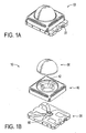
- Figure 1A is a perspective view of a semiconductor die package according to one embodiment of the present invention.
- Figure 1B is an exploded perspective view of the semiconductor package of Figure 1A ;
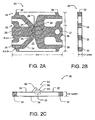
- Figure 2A is a top view of a portion of the semiconductor package of Figure 1A ;
- Figure 2B is a side view of a portion of the semiconductor package of Figure 1A ;
- Figure 2C is a front view of a portion of the semiconductor package of Figure 1A ;
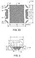
- Figure 2D is a bottom view of a portion of the semiconductor package of Figure 1A ;
- Figure 3 is a cut-away side view of portions of the semiconductor package of Figure 1A ;
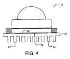
- Figure 4 is a side view of the semiconductor package of Figure 1A with additional elements;
- Figure 5 an exploded perspective view of a semiconductor die package according to another embodiment of the present invention.
- Figure 6A is a top view of a portion of the semiconductor package of Figure 5 ;
- Figure 6B is a side view of a portion of the semiconductor package of Figure 5 ;
- Figure 6C is a front view of a portion of the semiconductor package of Figure 5 ;
- Figure 6D is a bottom view of a portion of the semiconductor package of Figure 5 .
- relative terms such as beneath may be used herein to describe one layer or regions relationship to another layer or region as illustrated in the Figures. It will be understood that these terms are intended to encompass different orientations of the device in addition to the orientation depicted in the Figures. For example, if the device in the Figures is turned over, layers or regions described as “beneath” other layers or regions would now be oriented “above” these other layers or regions. The term “beneath” is intended to encompass both above and beneath in this situation. Like numbers refer to like elements throughout.
- a light emitting die package including a bottom heat sink (substrate) having traces for connecting to a light emitting diode at a mounting pad and a top heat sink (reflector plate) substantially surrounding the mounting pad.
- a lens covers the mounting pad.
- the die package according to some embodiments of the present invention comprises a two part heat sink with the bottom heat sink utilized (in additional to its utility for drawing and dissipating heat) as the substrate on which the LED is mounted and connected, and the top heat sink utilized (in additional to its utility for drawing and dissipating heat) as a reflector plate to direct light produced by the LED. Because both the bottom and the top heat sinks draw heat away from the LED, more power can be delivered to the LED, and the LED can thereby produce more light.
- the body of the die package itself may act as the heat' sink removing heat from the LED and dissipating it.
- the LED die package of the present invention may not require a separate heat sink slugs or leads that extend away from the package. Accordingly, the LED die package of the present invention may be more compact, more reliable, and less costly to manufacture than the die packages of the prior art.
- Figure 1A is a perspective view of a semiconductor die package 10 according to one embodiment of the present invention and Figure 1B is an exploded perspective view of the semiconductor package of Figure 1A .
- the light emitting die package 10 of the present invention includes a bottom heat sink 20, a top heat sink 40, and a lens 50.
- the bottom heat sink 20 is illustrated in more detail in Figures 2A through 2D .
- Figures 2A, 2B, 2C , and 2D provide, respectively, a top view, a side view, a front view, and a bottom view of the bottom heat sink 20 of Figure 1A .
- Figure 2C also shows an LED assembly 60 in addition to the front view of the bottom heat sink 20.
- the LED assembly 60 is also illustrated in Figure 1B .
- the bottom heat sink 20 provides support for electrical traces 22 and 24; for solder pads 26, 32, and 34; and for the LED assembly 60.
- the bottom heat sink 20 is also referred to as a substrate 20.
- solder pads 26, 32, and 34 are indicated with reference numbers.
- the traces 22 and 24 and the solder pads 32, 34, and 36 can be fabricated using conductive material. Further, additional traces and connections can be fabricated on the top, side, or bottom of the substrate 20, or layered within the substrate 20.
- the traces 22 and 24, the solder pads 32, 34, and 36, and any other connections can be interconnected to each other in any combinations using known methods, for example via holes.
- the substrate 20 is made of material having high thermal conductivity but is electrically insulating, for example, aluminum nitride (AlN) or alumina (Al 2 O 3 ). Dimensions of the substrate 20 can vary widely depending on application and processes used to manufacture the die package 10. For example, in the illustrated embodiment, the substrate 20 may have dimensions ranging from fractions of millimeters (mm) to tens of millimeters. Although the present invention is not limited to particular dimensions, one specific embodiment of the die package 10 of the present invention is illustrated in Figures having the dimensions denoted therein. All dimensions shown in the Figures are in millimeters (for lengths, widths, heights, and radii) and degrees (for angles) except as otherwise designated in the Figures, in the Specification herein, or both.
- the substrate 20, in the illustrated embodiment, has a top surface 21, the top surface 21 including the electrical traces 22 and 24.
- the traces 22 and 24 provide electrical connections from the solder pads (for example top solder pads 26) to a mounting pad 28.
- the top solder pads 26 are portions of the traces 22 and 24 generally proximal to sides of the substrate 20.
- the top solder pads 26 are electrically connected to side solder pads 32.
- the mounting pad 28 is a portion of the top surface (including portions of the trace 22, the trace 24, or both) where the LED assembly 60 is mounted. Typically the mounting pad 28 is generally located proximal to center of the top surface 21. In alternative embodiments of the present invention, the LED assembly 60 can be replaced by other semiconductor circuits or chips.
- the traces 22 and 24 provide electrical routes to allow the LED assembly 60 to electrically connect to the solder pads 26, 32, or 34. Accordingly, some of the traces are referred to as first traces 22 while other traces are referred to as second traces 24.
- the mounting pad 28 includes portions of both the first traces 22 and the second traces 24.
- the LED assembly 60 is placed on the first trace 22 portion of the mounting pad 28 thereby making contact with the first trace 22.
- top of the LED assembly 60 and the second traces 24 are connected to each other via a bond wire 62.
- first traces 22 may provide anode (positive) connections and second traces 24 may comprise, cathode (negative) connections for the LED assembly 60 (or vice versa).
- the LED assembly 60 can include additional elements.
- the LED assembly 60 is illustrated including the LED bond wire 62, an LED subassembly 64, and a light emitting diode (LED) 66.
- LED subassembly 64 is known in the art and is illustrated for the purposes of discussing the invention and is not meant to be a limitation of the present invention.
- the LED assembly 60 is shown die-attached to the substrate 20.
- the mounting pad 28 can be configured to allow flip-chip attachment of the LED assembly 60.
- multiple LED assemblies can be mounted on the mounting pad 28.
- the LED assembly 60 can be mounted over multiple traces. This is especially true if flip-chip technology is used.
- the topology of the traces 22 and 24 can vary widely from the topology illustrated in the Figures while still remaining within the scope of the present invention.
- three separate cathode (negative) traces 24 are shown to illustrate that three LED assemblies can be placed on the mounting pad 28, each connected to a different cathode (negative) trace; thus, the three LED assemblies may be separately electrically controllable.
- the traces 22 and 24 are made of conductive material such as gold, silver, tin, or other metals.
- the traces 22 and 24 can have dimensions as illustrated in the Figures and having thickness in the order of microns or tens of microns depending on application. For example, the traces 22 and 24 can be 15 microns thick.
- Figures 1A and 2A illustrate an orientation marking 27. Such markings can be used to identify the proper orientation of the die package 10 even after assembling the die package 10.
- the orientation marking 27 is not a via or a through hole.
- the traces 22 and 24, as illustrated, can extend from the mounting pad 28 to sides
- the substrate 20 defines semi-cylindrical spaces 23 and quarter-cylindrical spaces 25 proximal to its sides.
- the semi-cylindrical spaces 23 and the quarter-cylindrical spaces 25 provide spaces for solder to flow-through and solidify-in when the die package 10 is attached to a printed circuit board (PCB) or another apparatus (not shown) to which the die package 10 is a component thereof.
- the semi-cylindrical spaces 23 and the quarter-cylindrical spaces 25 provide convenient delineation and break points during the manufacturing process.
- the substrate 20 can be manufactured as one individual section of a strip or a plate having a plurality of adjacent sections, each section being a substrate 20.
- the substrate 20 can be manufactured as one individual section of an array of sections, the array having multiple rows and columns of adjacent sections.
- the semi-cylindrical spaces 23 and quarter-cylindrical spaces 25 can be utilized as tooling holes for the strip, the plate, or the array during the manufacturing process.
- the semi-cylindrical spaces 23 and the quarter-cylindrical spaces 25 combined with scribed grooves or other etchings between the sections, assist in separating each individual substrate from the strip, the plate, or the wafer.
- the separation can be accomplished by introducing physical stress to the perforation (semi through holes at a close pitch) or scribe lines made by laser, or premolded, or etched lines (crossing the semi-cylindrical spaces 23 and the quarter-cylindrical spaces 25) by bending the strip, the plate, or the wafer.
- the semi-cylindrical spaces 23 and the quarter-cylindrical spaces 25 serve as via holes connecting the top solder pads 26, the side solder pads 32, and the bottom solder pads 34.
- the substrate 20 has a bottom surface 29 including a thermal contact pad 36.
- the thermal contact pad 36 can be fabricated using material having high thermally and electrically conductive material such as gold, silver, tin, or other material including but not limited to precious metals.
- Figure 3 illustrates a cut-away side view of portions of the semiconductor package of Figures 1A and 1B .
- the Figure 3 illustrates a cut-away side view of the top heat sink 40 and the lens 50.
- the top heat sink 40 is made from material having high thermal conductivity such as aluminum, copper, ceramics, plastics, composites, or a combination of these materials.
- a high temperature, mechanically tough, dielectric material can be used to overcoat the traces 22 and 24 (with the exception of the central die-attach area) to seal the traces 22 and 24 and provide protection from physical and environmental harm such as scratches and oxidation.
- the overcoating process can be a part of the substrate manufacturing process.
- the overcoat when used, may insulate the substrate 20 from the top heat sink 40.
- the overcoat may then be covered with a high temperature adhesive such as thermal interface material manufactured by THERMOSET that bonds the substrate 20 to the top heat sink 40.
- the top heat sink 40 may include a reflective surface 42 substantially surrounding the LED assembly 60 mounted on the mounting pad 28 (of Figures 2A and 2C ).
- the top heat sink 40 When the top heat sink 40 is used to dissipate heat generated by the LED in the die package 10, it can be "top-mounted” directly on to an external heat sink by an adhesive or solder joint to dissipate heat efficiently.
- the top heat sink 40 may be made to equip with cooling fins or any feature that will enhance heat transfer between the top heat sink 40 and the cooling medium.
- the electrical terminals and the bottom heat sink 20 of the die package 10 can still be connected to its application printed circuit board (PCB) using, for example, the normal surface-mount-technology (SMT) method.
- PCB application printed circuit board
- the reflective surface 42 reflects portions of light from the LED assembly 60 as illustrated by sample light rays 63. Other portions of the light are not reflected by the reflective surface 42 as illustrated by sample light ray 61. Illustrative light rays 61 and 63 are not meant to represent light traces often use in the optical arts.
- the top heat sink 40 is preferably made from material that can be polished, coined, molded, or any combination of these. Alternatively, to achieve high reflectivity, the optical reflective surface 42 or the entire heat sink 40 can be plated or deposited with high reflective material such as silver, aluminum, or any substance that serves the purpose. For this reason, the top heat sink 40 is also referred to as a reflector plate 40.
- the reflector plate 40 is made of material having high thermal conductivity if and when required by the thermal performance of the package 10.
- the reflective surface 42 is illustrated as a flat surface at an angle, for example 45 degrees, relative to the reflective plate's horizontal plane.
- the present invention is not limited to the illustrated embodiment.
- the reflective surface 42 can be at a different angle relative to the reflective plate's horizontal plane.
- the reflective plate can have a parabolic, toroid or any other shape that helps to meet the desired spectral luminous performance of the package.
- the reflective plate 40 includes a ledge 44 for supporting and coupling with the lens 50.
- the LED assembly 60 is encapsulated within the die package 10 (of Figures 1A and 1B ) using encapsulation material 46 such as, for example only, soft and elastic silicones or polymers.
- the encapsulation material 46 is preferably high temperature polymer with high light transmissivity and refractive index that matches or closely matches refractive index of the lens 50.
- the encapsulant 46 is preferably not affected by most wavelengths that alter its light transmissivity or clarity.
- the lens 50 is made from material having high light transmissivity such as, for example only, glass, quartz, high temperature and transparent plastic, or a combination of these materials.
- the lens 50 is placed on top of and adheres to the encapsulation material 46.
- the lens 50 is not rigidly bonded to the reflector 40.
- This "floating lens" design will ensure that the encapsulant 46 can expand and contract under high and low temperature conditions without problem. For instance, when the die package 10 is operating or being subjected to high temperature environment, encapsulant 46 experiences greater volumetric expansion than the cavity space that contains it. By allowing the lens 50 to float up somewhat freely on top of the encapsulant 46, no encapsulant will be squeezed out of its cavity space.
- the encapsulant 46 will contract more than the other components that make up the cavity space for the encapsulant 46; the lens will float freely on top of the encapsulant 46 as the latter shrinks and its level drops. Hence, the reliability of the die package 10 is maintained over a relatively large temperature ranges as the thermal stresses induced on its encapsulant 46 is reduced by the floating lens design.
- the lens 50 defines a recess 52 having a curved, hemispherical, or other geometry, which can be filled with optical materials intended to influence or change the nature of the light emitted by the LED chip(s) before it leaves the die package 10.
- optical materials include luminescence converting phosphors, dyes, fluorescent polymers or other materials which absorb some of the light emitted by the chip(s) and re-emit light of different wavelengths.
- Examples of another type of optical materials are light diffusants such as calcium carbonate, scattering particles (such as Titanium oxides) or voids which disperse or scatter light. Any single or combination of the above materials can be applied on the lens to obtain certain spectral luminous performance.
- FIG 4 illustrates the die package 10 coupled to an external heat sink 70.
- the thermal contact pad 36 can be attached to the external heat sink 70 using epoxy, solder, or any other thermally conductive adhesive, electrically conductive adhesive, or thermally and electrically conductive adhesive 74.
- the external heat sink 70 can be a printed circuit board (PCB) or other structure that draws heat from the die package 10.
- the external heat sink can include circuit elements (not shown) or heat dissipation fins 72 in various configurations.
- FIG. 5 through 6D An embodiment of the invention having certain alternate configuration is shown in Figures 5 through 6D . Portions of this second embodiment are similar to corresponding portions of the first embodiment illustrated in Figures 1A through 4 . For convenience, portions of the second embodiment as illustrated in Figures 5 through 6D that are similar to portions of the first embodiment are assigned the same reference numerals, analogous but changed portions are assigned the same reference numerals accompanied by letter "a,” and different portions are assigned different reference numerals.
- FIG. 5 is an exploded perspective view of an LED die package 10a in accordance with other embodiments of the present invention.
- the light emitting die package 10a of the present invention includes a bottom heat sink (substrate) 20a, a top heat sink (reflector plate) 40a, and a lens 50.
- Figures 6A, 6B, 6C, and 6D provide, respectively, a top view, a side view a front view, and a bottom view of the substrate 20a of Figure 5 .
- the substrate 20a includes one first trace 22a and four second traces 24a. These traces 22a and 24a have are configured differently than the traces 22 and 24 of Figure 2A .
- the substrate 20a includes flanges 31 that define latch spaces 33 for reception of legs 35 of the reflector plate 40a thereby mechanically engaging the reflector plate 40a with the substrate 20a.
Abstract
Description
- The present invention relates to a light-emitting die package.
- From
U.S. 2002/0084462 A1 a light-emitting die package is known which includes a light emitter, a light reflection member, and a resin sealing the light emitter by covering the light reflection member and the light emitter. Light deviated from a predetermined front region in the light emitted from the light emitter is totally reflected by a boundary surface of the resin to be forwardly emitted by the light reflection member, and the emitter is thermally contacted with the reflection member to dissipate the heat generated from the light emitter. Particularly, the lens is integrally formed with the encapsulating mold resin. - Light emitting diodes (LEDS) are often packaged within leadframe packages. A leadframe package typically includes a molded or cast plastic body that encapsulates an LED, a lens portion, and thin metal leads connected to the LED and extending outside the body. The metal leads of the leadframe package serve as the conduit to supply the LED with electrical power and, at the same time, may act to draw heat away from the LED. Heat is generated by the LED when power is applied to the LED to produce light. A portion of the leads extends out from the package body for connection to circuits external to the leadframe package.
- Some of the heat generated by the LED is dissipated by the plastic package body; however, most of the heat is drawn away from the LED via the metal components of the package. The metal leads are typically very thin and has a small cross section. For this reason, capacity of the metal leads to remove heat from the LED is limited. This limits the amount of power that can be sent to the LED thereby limiting the amount of light that can be generated by the LED.
- To increase the capacity of an LED package to dissipate heat, in one LED package design, a heat sink slug is introduced into the package. The heat sink slug draws heat from the LED chip. Hence, it increases the capacity of the LED package to dissipate heat. However, this design introduces empty spaces within the package that is be filled with an encapsulant to protect the LED chip. Furthermore, due to significant differences in CTE (coefficient of thermal expansion) between various components inside the LED package, bubbles tend to form inside the encapsulant or the encapsulant tends to delaminate from various portions within the package. This adversely affects the light output and reliability of the product. In addition, this design includes a pair of flimsy leads which are typically soldered by a hot-iron. This manufacturing process is incompatible with convenient surface mounting technology (SMT) that is popular in the art of electronic board assembly.
- In another LED package design, the leads of the leadframe package have differing thicknesses extended (in various shapes and configurations) beyond the immediate edge of the LED package body. A thicker lead is utilized as a heat-spreader and the LED chip is mounted on it. This arrangement allows heat generated by the LED chip to dissipate through the thicker lead which is often connected to an external heat sink. This design is inherently unreliable due to significant difference in coefficient of thermal expansion (CTE) between the plastic body and the leadframe material. When subjected to temperature cycles, its rigid plastic body that adheres to the metal leads experiences high degree of thermal stresses in many directions. This potentially leads to various undesirable results such as cracking of the plastic body, separation of the plastic body from the LED chip, breaking of the bond wires, delaminating of the plastic body at the interfaces where it bonds to various parts, or resulting in a combination of these outcomes. In addition, the extended leads increase the package size and its footprint. For this reason, it is difficult to populate these LED packages in a dense cluster on a printed circuit board (PCB) to generate brighter light.
- Another disadvantage of the current leadframe design is that the thick lead cannot be made or stamped into a fine circuit for flip-chip mounting of a LED - which is commonly used by some manufacturers for cost-effective manufacturing and device performance.
- Consequently, there remains a need for an improved LED package that overcomes or alleviates one or more of the shortcomings of the prior art packages.
- The need is met by the present invention as defined in
independent claim 1. Embodiments of the present invention provide a package for a semiconductor die such as a light emitting diode, the package including a substrate having traces for connecting to a light emitting diode at a mounting pad, a reflector plate coupled to the substrate and substantially surrounding the mounting pad, and lens substantially covering the mounting pad. - Other embodiments of the present invention provide a semiconductor die package includes a bottom heat sink and a top heat sink. The bottom heat sink has traces on its top surface. A semiconductor chip is mounted on the top surface of the bottom heat sink and electrically connected to the traces. The top heat sink is coupled to the bottom heat sink.
- Other aspects and advantages of the present invention will become apparent from the following detailed description, taken in conjunction with the accompanying drawings, illustrating by way of example the principles of the invention.
-
Figure 1A is a perspective view of a semiconductor die package according to one embodiment of the present invention; -
Figure 1B is an exploded perspective view of the semiconductor package ofFigure 1A ; -
Figure 2A is a top view of a portion of the semiconductor package ofFigure 1A ; -
Figure 2B is a side view of a portion of the semiconductor package ofFigure 1A ; -
Figure 2C is a front view of a portion of the semiconductor package ofFigure 1A ; -
Figure 2D is a bottom view of a portion of the semiconductor package ofFigure 1A ; -
Figure 3 is a cut-away side view of portions of the semiconductor package ofFigure 1A ; -
Figure 4 is a side view of the semiconductor package ofFigure 1A with additional elements; -
Figure 5 an exploded perspective view of a semiconductor die package according to another embodiment of the present invention; -
Figure 6A is a top view of a portion of the semiconductor package ofFigure 5 ; -
Figure 6B is a side view of a portion of the semiconductor package ofFigure 5 ; -
Figure 6C is a front view of a portion of the semiconductor package ofFigure 5 ; and -
Figure 6D is a bottom view of a portion of the semiconductor package ofFigure 5 . - The present invention will now be described with reference to the
Figures 1 through 6D , which illustrate various embodiments of the present invention. As illustrated in the Figures, the sizes of layers or regions are exaggerated for illustrative purposes and, thus, are provided to illustrate the general structures of the present invention. Furthermore, various aspects of the present invention are described with reference to a layer or structure being formed on a substrate or other layer or structure. As will be appreciated by those of skill in the art, references to a layer being formed "on" another layer or substrate contemplates that additional layers may intervene. References to a layer being formed on another layer or substrate without an intervening layer are described herein as being formed "directly on" the layer or substrate. Furthermore, relative terms such as beneath may be used herein to describe one layer or regions relationship to another layer or region as illustrated in the Figures. It will be understood that these terms are intended to encompass different orientations of the device in addition to the orientation depicted in the Figures. For example, if the device in the Figures is turned over, layers or regions described as "beneath" other layers or regions would now be oriented "above" these other layers or regions. The term "beneath" is intended to encompass both above and beneath in this situation. Like numbers refer to like elements throughout. - As shown in the figures for the purposes of illustration, embodiments of the present invention are exemplified by a light emitting die package including a bottom heat sink (substrate) having traces for connecting to a light emitting diode at a mounting pad and a top heat sink (reflector plate) substantially surrounding the mounting pad. A lens covers the mounting pad. In effect, the die package according to some embodiments of the present invention comprises a two part heat sink with the bottom heat sink utilized (in additional to its utility for drawing and dissipating heat) as the substrate on which the LED is mounted and connected, and the top heat sink utilized (in additional to its utility for drawing and dissipating heat) as a reflector plate to direct light produced by the LED. Because both the bottom and the top heat sinks draw heat away from the LED, more power can be delivered to the LED, and the LED can thereby produce more light.
- Further, in the present invention, the body of the die package itself may act as the heat' sink removing heat from the LED and dissipating it. For this reason, the LED die package of the present invention may not require a separate heat sink slugs or leads that extend away from the package. Accordingly, the LED die package of the present invention may be more compact, more reliable, and less costly to manufacture than the die packages of the prior art.
-
Figure 1A is a perspective view of asemiconductor die package 10 according to one embodiment of the present invention andFigure 1B is an exploded perspective view of the semiconductor package ofFigure 1A . Referring toFigures 1A and 1B , the light emittingdie package 10 of the present invention includes abottom heat sink 20, atop heat sink 40, and alens 50. - The
bottom heat sink 20 is illustrated in more detail inFigures 2A through 2D .Figures 2A, 2B, 2C , and2D provide, respectively, a top view, a side view, a front view, and a bottom view of thebottom heat sink 20 ofFigure 1A . Further,Figure 2C also shows anLED assembly 60 in addition to the front view of thebottom heat sink 20. TheLED assembly 60 is also illustrated inFigure 1B . Referring toFigures 1A through 2D , thebottom heat sink 20 provides support forelectrical traces solder pads LED assembly 60. For this reason, thebottom heat sink 20 is also referred to as asubstrate 20. In the Figures, to avoid clutter, onlyrepresentative solder pads traces solder pads substrate 20, or layered within thesubstrate 20. Thetraces solder pads - The
substrate 20 is made of material having high thermal conductivity but is electrically insulating, for example, aluminum nitride (AlN) or alumina (Al2O3). Dimensions of thesubstrate 20 can vary widely depending on application and processes used to manufacture thedie package 10. For example, in the illustrated embodiment, thesubstrate 20 may have dimensions ranging from fractions of millimeters (mm) to tens of millimeters. Although the present invention is not limited to particular dimensions, one specific embodiment of thedie package 10 of the present invention is illustrated in Figures having the dimensions denoted therein. All dimensions shown in the Figures are in millimeters (for lengths, widths, heights, and radii) and degrees (for angles) except as otherwise designated in the Figures, in the Specification herein, or both. - The
substrate 20, in the illustrated embodiment, has atop surface 21, thetop surface 21 including theelectrical traces traces pad 28. Thetop solder pads 26 are portions of thetraces substrate 20. Thetop solder pads 26 are electrically connected toside solder pads 32. The mountingpad 28 is a portion of the top surface (including portions of thetrace 22, thetrace 24, or both) where theLED assembly 60 is mounted. Typically the mountingpad 28 is generally located proximal to center of thetop surface 21. In alternative embodiments of the present invention, theLED assembly 60 can be replaced by other semiconductor circuits or chips. - The
traces LED assembly 60 to electrically connect to thesolder pads first traces 22 while other traces are referred to as second traces 24. In the illustrated embodiment, the mountingpad 28 includes portions of both the first traces 22 and the second traces 24. In the illustrated example, theLED assembly 60 is placed on thefirst trace 22 portion of the mountingpad 28 thereby making contact with thefirst trace 22. In the illustrated embodiment, top of theLED assembly 60 and the second traces 24 are connected to each other via abond wire 62. Depending on the construction and orientation ofLED assembly 60, first traces 22 may provide anode (positive) connections andsecond traces 24 may comprise, cathode (negative) connections for the LED assembly 60 (or vice versa). - The
LED assembly 60 can include additional elements. For example, inFigures 1B and2C , theLED assembly 60 is illustrated including theLED bond wire 62, anLED subassembly 64, and a light emitting diode (LED) 66.Such LED subassembly 64 is known in the art and is illustrated for the purposes of discussing the invention and is not meant to be a limitation of the present invention. In the Figures, theLED assembly 60 is shown die-attached to thesubstrate 20. In alternative embodiments, the mountingpad 28 can be configured to allow flip-chip attachment of theLED assembly 60. Additionally, multiple LED assemblies can be mounted on the mountingpad 28. In alternative embodiments, theLED assembly 60 can be mounted over multiple traces. This is especially true if flip-chip technology is used. - The topology of the
traces pad 28, each connected to a different cathode (negative) trace; thus, the three LED assemblies may be separately electrically controllable. Thetraces traces traces Figures 1A and2A illustrate an orientation marking 27. Such markings can be used to identify the proper orientation of thedie package 10 even after assembling thedie package 10. The orientation marking 27 is not a via or a through hole. Thetraces pad 28 to sides of thesubstrate 20. - Continuing to refer to
Figures 1A through 2D , thesubstrate 20 definessemi-cylindrical spaces 23 and quarter-cylindrical spaces 25 proximal to its sides. In the Figures, to avoid clutter, onlyrepresentative spaces semi-cylindrical spaces 23 and the quarter-cylindrical spaces 25 provide spaces for solder to flow-through and solidify-in when thedie package 10 is attached to a printed circuit board (PCB) or another apparatus (not shown) to which thedie package 10 is a component thereof. Moreover, thesemi-cylindrical spaces 23 and the quarter-cylindrical spaces 25 provide convenient delineation and break points during the manufacturing process. - The
substrate 20 can be manufactured as one individual section of a strip or a plate having a plurality of adjacent sections, each section being asubstrate 20. Alternatively, thesubstrate 20 can be manufactured as one individual section of an array of sections, the array having multiple rows and columns of adjacent sections. In such configuration, thesemi-cylindrical spaces 23 and quarter-cylindrical spaces 25 can be utilized as tooling holes for the strip, the plate, or the array during the manufacturing process. - Furthermore, the
semi-cylindrical spaces 23 and the quarter-cylindrical spaces 25, combined with scribed grooves or other etchings between the sections, assist in separating each individual substrate from the strip, the plate, or the wafer. The separation can be accomplished by introducing physical stress to the perforation (semi through holes at a close pitch) or scribe lines made by laser, or premolded, or etched lines (crossing thesemi-cylindrical spaces 23 and the quarter-cylindrical spaces 25) by bending the strip, the plate, or the wafer. These features simplify the manufacturing process thus reducing costs by eliminating the need for special carrier fixtures to handle individual unit of thesubstrate 20 during the manufacturing process. Furthermore, thesemi-cylindrical spaces 23 and the quarter-cylindrical spaces 25 serve as via holes connecting thetop solder pads 26, theside solder pads 32, and thebottom solder pads 34. - The
substrate 20 has abottom surface 29 including athermal contact pad 36. Thethermal contact pad 36 can be fabricated using material having high thermally and electrically conductive material such as gold, silver, tin, or other material including but not limited to precious metals. -
Figure 3 illustrates a cut-away side view of portions of the semiconductor package ofFigures 1A and 1B . In particular, theFigure 3 illustrates a cut-away side view of thetop heat sink 40 and thelens 50. Referring toFigures 1A, 1B , and3 , thetop heat sink 40 is made from material having high thermal conductivity such as aluminum, copper, ceramics, plastics, composites, or a combination of these materials. A high temperature, mechanically tough, dielectric material can be used to overcoat thetraces 22 and 24 (with the exception of the central die-attach area) to seal thetraces substrate 20 from thetop heat sink 40. The overcoat may then be covered with a high temperature adhesive such as thermal interface material manufactured by THERMOSET that bonds thesubstrate 20 to thetop heat sink 40. - The
top heat sink 40 may include areflective surface 42 substantially surrounding theLED assembly 60 mounted on the mounting pad 28 (ofFigures 2A and 2C ). When thetop heat sink 40 is used to dissipate heat generated by the LED in thedie package 10, it can be "top-mounted" directly on to an external heat sink by an adhesive or solder joint to dissipate heat efficiently. In another embodiment, if heat has to be dissipated by either a compressible or non-compressible medium such as air or cooling fluid, thetop heat sink 40 may be made to equip with cooling fins or any feature that will enhance heat transfer between thetop heat sink 40 and the cooling medium. In both of these embodiments, the electrical terminals and thebottom heat sink 20 of thedie package 10, can still be connected to its application printed circuit board (PCB) using, for example, the normal surface-mount-technology (SMT) method. - The
reflective surface 42 reflects portions of light from theLED assembly 60 as illustrated by sample light rays 63. Other portions of the light are not reflected by thereflective surface 42 as illustrated bysample light ray 61. Illustrativelight rays top heat sink 40 is preferably made from material that can be polished, coined, molded, or any combination of these. Alternatively, to achieve high reflectivity, the opticalreflective surface 42 or theentire heat sink 40 can be plated or deposited with high reflective material such as silver, aluminum, or any substance that serves the purpose. For this reason, thetop heat sink 40 is also referred to as areflector plate 40. Thereflector plate 40 is made of material having high thermal conductivity if and when required by the thermal performance of thepackage 10. In the illustrated embodiment, thereflective surface 42 is illustrated as a flat surface at an angle, for example 45 degrees, relative to the reflective plate's horizontal plane. The present invention is not limited to the illustrated embodiment. For example, thereflective surface 42 can be at a different angle relative to the reflective plate's horizontal plane. Alternatively, the reflective plate can have a parabolic, toroid or any other shape that helps to meet the desired spectral luminous performance of the package. - The
reflective plate 40 includes aledge 44 for supporting and coupling with thelens 50. TheLED assembly 60 is encapsulated within the die package 10 (ofFigures 1A and 1B ) usingencapsulation material 46 such as, for example only, soft and elastic silicones or polymers. Theencapsulation material 46 is preferably high temperature polymer with high light transmissivity and refractive index that matches or closely matches refractive index of thelens 50. Theencapsulant 46 is preferably not affected by most wavelengths that alter its light transmissivity or clarity. - The
lens 50 is made from material having high light transmissivity such as, for example only, glass, quartz, high temperature and transparent plastic, or a combination of these materials. Thelens 50 is placed on top of and adheres to theencapsulation material 46. Thelens 50 is not rigidly bonded to thereflector 40. This "floating lens" design will ensure that theencapsulant 46 can expand and contract under high and low temperature conditions without problem. For instance, when thedie package 10 is operating or being subjected to high temperature environment, encapsulant 46 experiences greater volumetric expansion than the cavity space that contains it. By allowing thelens 50 to float up somewhat freely on top of theencapsulant 46, no encapsulant will be squeezed out of its cavity space. Likewise, when thedie package 10 is subjected to cold temperature, theencapsulant 46 will contract more than the other components that make up the cavity space for theencapsulant 46; the lens will float freely on top of theencapsulant 46 as the latter shrinks and its level drops. Hence, the reliability of thedie package 10 is maintained over a relatively large temperature ranges as the thermal stresses induced on itsencapsulant 46 is reduced by the floating lens design. - In some embodiments, the
lens 50 defines arecess 52 having a curved, hemispherical, or other geometry, which can be filled with optical materials intended to influence or change the nature of the light emitted by the LED chip(s) before it leaves thedie package 10. Examples of one type of optical materials are luminescence converting phosphors, dyes, fluorescent polymers or other materials which absorb some of the light emitted by the chip(s) and re-emit light of different wavelengths. Examples of another type of optical materials are light diffusants such as calcium carbonate, scattering particles (such as Titanium oxides) or voids which disperse or scatter light. Any single or combination of the above materials can be applied on the lens to obtain certain spectral luminous performance. -
Figure 4 illustrates thedie package 10 coupled to anexternal heat sink 70. Referring toFigure 4 , thethermal contact pad 36 can be attached to theexternal heat sink 70 using epoxy, solder, or any other thermally conductive adhesive, electrically conductive adhesive, or thermally and electricallyconductive adhesive 74. Theexternal heat sink 70 can be a printed circuit board (PCB) or other structure that draws heat from thedie package 10. The external heat sink can include circuit elements (not shown) orheat dissipation fins 72 in various configurations. - An embodiment of the invention having certain alternate configuration is shown in
Figures 5 through 6D . Portions of this second embodiment are similar to corresponding portions of the first embodiment illustrated inFigures 1A through 4 . For convenience, portions of the second embodiment as illustrated inFigures 5 through 6D that are similar to portions of the first embodiment are assigned the same reference numerals, analogous but changed portions are assigned the same reference numerals accompanied by letter "a," and different portions are assigned different reference numerals. -
Figure 5 is an exploded perspective view of anLED die package 10a in accordance with other embodiments of the present invention. Referring toFigure 5 , the light emittingdie package 10a of the present invention includes a bottom heat sink (substrate) 20a, a top heat sink (reflector plate) 40a, and alens 50. -
Figures 6A, 6B, 6C, and 6D , provide, respectively, a top view, a side view a front view, and a bottom view of thesubstrate 20a ofFigure 5 . Referring toFigures 5 through 6D , in the illustrated embodiment, thesubstrate 20a includes onefirst trace 22a and foursecond traces 24a. Thesetraces traces Figure 2A . Thesubstrate 20a includesflanges 31 that definelatch spaces 33 for reception oflegs 35 of thereflector plate 40a thereby mechanically engaging thereflector plate 40a with thesubstrate 20a.
Claims (12)
- A light emitting die package (10; 10a), comprising:a substrate (20; 20a) supporting an LED chip (66) thereon that is encapsulated within a encapsulant (46);a reflector plate (40; 40a) on the substrate, said reflector plate (40; 40a) substantially surrounding the LED chip (66) and having a circular-opening which forms a circular sidewall within the reflector plate; anda lens (50) which sits within the opening on top of the encapsulant and which adheres to the encapsulant, the lens being free to move relative to the circular sidewall of the reflector plate as the encapsulant expands and contracts.
- A light emitting die package (10, 10a) according to claim 1, wherein each of the substrate (20, 20a) and reflector plate (40, 40a) have a heat sink capability to draw away heat generated by the LED chip (66) during package operation.
- A light emitting die package (10; 10a) according to Claim 1, wherein the reflector plate (40; 40a) is mechanically coupled to the substrate (20; 20a).
- A light emitting die package (10a) according to Claim 3, wherein the substrate (20a) includes flanges (31) along at least one side thereof for mechanically engaging the reflector plate (40a).
- The light emitting die package (10a) of claim 4, wherein the reflector plate (40a) includes legs (35) for mechanically engaging the substrate (20a) between the flanges (31) for increased thermal contact area.
- The light emitting die package (10; 10a) of claim 1, wherein the substrate (20; 20a) comprises an electrically insulating material having high thermal conductivity.
- The light emitting die package (10; 10a) of claim 6, wherein the substrate (20; 20a) has a bottom side with a thermal contact pad (36) for coupling with an external heat sink (70).
- The light emitting die package (10; 10a) of claim 7, further comprising an external heat sink (70) coupled to the substrate (20; 20a).
- The light emitting die package (10; 10a) of claim 1, wherein the lens (50) is composed of a material selected from a group consisting of glass, quartz, and a high temperature plastic material.
- The light emitting die package (10; 10a) of claim 1, wherein the lens (50) includes luminescence converting phosphors.
- The light emitting die package (10; 10a) of claim 1, wherein the lens (50) includes an optical diffusant.
- The light emitting die package of claim 1, wherein the lens (50) includes a phosphor.
Applications Claiming Priority (3)
| Application Number | Priority Date | Filing Date | Title |
|---|---|---|---|
| US40825402P | 2002-09-04 | 2002-09-04 | |
| US10/446,532 US7264378B2 (en) | 2002-09-04 | 2003-05-27 | Power surface mount light emitting die package |
| EP03794564A EP1537603B1 (en) | 2002-09-04 | 2003-09-02 | Power surface mount light emitting die package |
Related Parent Applications (2)
| Application Number | Title | Priority Date | Filing Date |
|---|---|---|---|
| EP03794564.9 Division | 2003-09-02 | ||
| EP03794564A Division EP1537603B1 (en) | 2002-09-04 | 2003-09-02 | Power surface mount light emitting die package |
Publications (3)
| Publication Number | Publication Date |
|---|---|
| EP1953825A2 EP1953825A2 (en) | 2008-08-06 |
| EP1953825A3 EP1953825A3 (en) | 2008-09-17 |
| EP1953825B1 true EP1953825B1 (en) | 2013-07-24 |
Family
ID=31981582
Family Applications (2)
| Application Number | Title | Priority Date | Filing Date |
|---|---|---|---|
| EP08157294.3A Expired - Lifetime EP1953825B1 (en) | 2002-09-04 | 2003-09-02 | Power surface mount light emitting die package |
| EP03794564A Expired - Lifetime EP1537603B1 (en) | 2002-09-04 | 2003-09-02 | Power surface mount light emitting die package |
Family Applications After (1)
| Application Number | Title | Priority Date | Filing Date |
|---|---|---|---|
| EP03794564A Expired - Lifetime EP1537603B1 (en) | 2002-09-04 | 2003-09-02 | Power surface mount light emitting die package |
Country Status (11)
| Country | Link |
|---|---|
| US (1) | US7264378B2 (en) |
| EP (2) | EP1953825B1 (en) |
| JP (8) | JP4731906B2 (en) |
| KR (5) | KR101082304B1 (en) |
| CN (1) | CN100414698C (en) |
| AT (1) | ATE400896T1 (en) |
| AU (1) | AU2003276860A1 (en) |
| CA (1) | CA2496937A1 (en) |
| DE (1) | DE60322074D1 (en) |
| TW (1) | TWI331380B (en) |
| WO (1) | WO2004023522A2 (en) |
Cited By (9)
| Publication number | Priority date | Publication date | Assignee | Title |
|---|---|---|---|---|
| US8530915B2 (en) | 2002-09-04 | 2013-09-10 | Cree, Inc. | Power surface mount light emitting die package |
| US8608349B2 (en) | 2002-09-04 | 2013-12-17 | Cree, Inc. | Power surface mount light emitting die package |
| US11297705B2 (en) | 2007-10-06 | 2022-04-05 | Lynk Labs, Inc. | Multi-voltage and multi-brightness LED lighting devices and methods of using same |
| US11317495B2 (en) | 2007-10-06 | 2022-04-26 | Lynk Labs, Inc. | LED circuits and assemblies |
| US11528792B2 (en) | 2004-02-25 | 2022-12-13 | Lynk Labs, Inc. | High frequency multi-voltage and multi-brightness LED lighting devices |
| US11566759B2 (en) | 2017-08-31 | 2023-01-31 | Lynk Labs, Inc. | LED lighting system and installation methods |
| US11638336B2 (en) | 2004-02-25 | 2023-04-25 | Lynk Labs, Inc. | AC light emitting diode and AC LED drive methods and apparatus |
| US11678420B2 (en) | 2004-02-25 | 2023-06-13 | Lynk Labs, Inc. | LED lighting system |
| US11953167B2 (en) | 2011-08-18 | 2024-04-09 | Lynk Labs, Inc. | Devices and systems having AC LED circuits and methods of driving the same |
Families Citing this family (258)
| Publication number | Priority date | Publication date | Assignee | Title |
|---|---|---|---|---|
| US10340424B2 (en) | 2002-08-30 | 2019-07-02 | GE Lighting Solutions, LLC | Light emitting diode component |
| US7479662B2 (en) | 2002-08-30 | 2009-01-20 | Lumination Llc | Coated LED with improved efficiency |
| US7800121B2 (en) | 2002-08-30 | 2010-09-21 | Lumination Llc | Light emitting diode component |
| US7264378B2 (en) * | 2002-09-04 | 2007-09-04 | Cree, Inc. | Power surface mount light emitting die package |
| US20050023260A1 (en) * | 2003-01-10 | 2005-02-03 | Shinya Takyu | Semiconductor wafer dividing apparatus and semiconductor device manufacturing method |
| EP1629537B1 (en) * | 2003-05-30 | 2014-07-30 | OSRAM Opto Semiconductors GmbH | Light-emitting diode |
| EP1484802B1 (en) * | 2003-06-06 | 2018-06-13 | Stanley Electric Co., Ltd. | Optical semiconductor device |
| JP2005073227A (en) * | 2003-08-04 | 2005-03-17 | Sharp Corp | Image pickup device |
| US20050104072A1 (en) | 2003-08-14 | 2005-05-19 | Slater David B.Jr. | Localized annealing of metal-silicon carbide ohmic contacts and devices so formed |
| US7183587B2 (en) * | 2003-09-09 | 2007-02-27 | Cree, Inc. | Solid metal block mounting substrates for semiconductor light emitting devices |
| US7915085B2 (en) | 2003-09-18 | 2011-03-29 | Cree, Inc. | Molded chip fabrication method |
| US7518158B2 (en) * | 2003-12-09 | 2009-04-14 | Cree, Inc. | Semiconductor light emitting devices and submounts |
| US7397067B2 (en) | 2003-12-31 | 2008-07-08 | Intel Corporation | Microdisplay packaging system |
| DE102004014207A1 (en) * | 2004-03-23 | 2005-10-13 | Osram Opto Semiconductors Gmbh | Optoelectronic component with a multi-part housing body |
| US7355284B2 (en) | 2004-03-29 | 2008-04-08 | Cree, Inc. | Semiconductor light emitting devices including flexible film having therein an optical element |
| US7517728B2 (en) * | 2004-03-31 | 2009-04-14 | Cree, Inc. | Semiconductor light emitting devices including a luminescent conversion element |
| JP4229447B2 (en) * | 2004-03-31 | 2009-02-25 | スタンレー電気株式会社 | Semiconductor light emitting device and manufacturing method |
| US7326583B2 (en) * | 2004-03-31 | 2008-02-05 | Cree, Inc. | Methods for packaging of a semiconductor light emitting device |
| US7279346B2 (en) * | 2004-03-31 | 2007-10-09 | Cree, Inc. | Method for packaging a light emitting device by one dispense then cure step followed by another |
| US20050225222A1 (en) * | 2004-04-09 | 2005-10-13 | Joseph Mazzochette | Light emitting diode arrays with improved light extraction |
| KR100643582B1 (en) | 2004-04-26 | 2006-11-10 | 루미마이크로 주식회사 | Light Emitting Diode package |
| US7361938B2 (en) | 2004-06-03 | 2008-04-22 | Philips Lumileds Lighting Company Llc | Luminescent ceramic for a light emitting device |
| US7280288B2 (en) * | 2004-06-04 | 2007-10-09 | Cree, Inc. | Composite optical lens with an integrated reflector |
| US7456499B2 (en) | 2004-06-04 | 2008-11-25 | Cree, Inc. | Power light emitting die package with reflecting lens and the method of making the same |
| CN101032034A (en) * | 2004-06-30 | 2007-09-05 | 克里公司 | Chip-scale methods for packaging light emitting devices and chip-scale packaged light emitting devices |
| KR100609734B1 (en) * | 2004-07-02 | 2006-08-08 | 럭스피아 주식회사 | Led package for use in back light of lcd and method of the same |
| US7252408B2 (en) * | 2004-07-19 | 2007-08-07 | Lamina Ceramics, Inc. | LED array package with internal feedback and control |
| US7118262B2 (en) * | 2004-07-23 | 2006-10-10 | Cree, Inc. | Reflective optical elements for semiconductor light emitting devices |
| US7201495B2 (en) * | 2004-08-03 | 2007-04-10 | Philips Lumileds Lighting Company, Llc | Semiconductor light emitting device package with cover with flexible portion |
| US7405093B2 (en) * | 2004-08-18 | 2008-07-29 | Cree, Inc. | Methods of assembly for a semiconductor light emitting device package |
| KR100604469B1 (en) * | 2004-08-25 | 2006-07-25 | 박병재 | light emitting device and package structure and method of manufacturing thereof |
| US7417220B2 (en) * | 2004-09-09 | 2008-08-26 | Toyoda Gosei Co., Ltd. | Solid state device and light-emitting element |
| US7855395B2 (en) * | 2004-09-10 | 2010-12-21 | Seoul Semiconductor Co., Ltd. | Light emitting diode package having multiple molding resins on a light emitting diode die |
| US7217583B2 (en) * | 2004-09-21 | 2007-05-15 | Cree, Inc. | Methods of coating semiconductor light emitting elements by evaporating solvent from a suspension |
| JP2006100633A (en) * | 2004-09-30 | 2006-04-13 | Toyoda Gosei Co Ltd | Led lighting device |
| US7812360B2 (en) * | 2004-10-04 | 2010-10-12 | Kabushiki Kaisha Toshiba | Light emitting device, lighting equipment or liquid crystal display device using such light emitting device |
| WO2006080729A1 (en) * | 2004-10-07 | 2006-08-03 | Seoul Semiconductor Co., Ltd. | Side illumination lens and luminescent device using the same |
| US20060097385A1 (en) | 2004-10-25 | 2006-05-11 | Negley Gerald H | Solid metal block semiconductor light emitting device mounting substrates and packages including cavities and heat sinks, and methods of packaging same |
| DE102005028748A1 (en) * | 2004-10-25 | 2006-05-04 | Osram Opto Semiconductors Gmbh | Electromagnetic radiation emitting semiconductor device and device package |
| US7772609B2 (en) * | 2004-10-29 | 2010-08-10 | Ledengin, Inc. (Cayman) | LED package with structure and materials for high heat dissipation |
| US9929326B2 (en) | 2004-10-29 | 2018-03-27 | Ledengin, Inc. | LED package having mushroom-shaped lens with volume diffuser |
| US20060091414A1 (en) * | 2004-10-29 | 2006-05-04 | Ouderkirk Andrew J | LED package with front surface heat extractor |
| US8324641B2 (en) * | 2007-06-29 | 2012-12-04 | Ledengin, Inc. | Matrix material including an embedded dispersion of beads for a light-emitting device |
| US8134292B2 (en) * | 2004-10-29 | 2012-03-13 | Ledengin, Inc. | Light emitting device with a thermal insulating and refractive index matching material |
| US7329982B2 (en) * | 2004-10-29 | 2008-02-12 | 3M Innovative Properties Company | LED package with non-bonded optical element |
| US8816369B2 (en) | 2004-10-29 | 2014-08-26 | Led Engin, Inc. | LED packages with mushroom shaped lenses and methods of manufacturing LED light-emitting devices |
| US7670872B2 (en) * | 2004-10-29 | 2010-03-02 | LED Engin, Inc. (Cayman) | Method of manufacturing ceramic LED packages |
| US7473933B2 (en) * | 2004-10-29 | 2009-01-06 | Ledengin, Inc. (Cayman) | High power LED package with universal bonding pads and interconnect arrangement |
| US20060124953A1 (en) * | 2004-12-14 | 2006-06-15 | Negley Gerald H | Semiconductor light emitting device mounting substrates and packages including cavities and cover plates, and methods of packaging same |
| EP1825524A4 (en) * | 2004-12-16 | 2010-06-16 | Seoul Semiconductor Co Ltd | Leadframe having a heat sink supporting ring, fabricating method of a light emitting diodepackage using the same and light emitting diodepackage fabbricated by the method |
| KR100580753B1 (en) * | 2004-12-17 | 2006-05-15 | 엘지이노텍 주식회사 | Light emitting device package |
| KR100646093B1 (en) * | 2004-12-17 | 2006-11-15 | 엘지이노텍 주식회사 | Light emitting device package |
| US7322732B2 (en) * | 2004-12-23 | 2008-01-29 | Cree, Inc. | Light emitting diode arrays for direct backlighting of liquid crystal displays |
| US8288942B2 (en) * | 2004-12-28 | 2012-10-16 | Cree, Inc. | High efficacy white LED |
| TWI248218B (en) * | 2004-12-31 | 2006-01-21 | Ind Tech Res Inst | Light-emitting diode package structure and fabrication method thereof |
| US7821023B2 (en) | 2005-01-10 | 2010-10-26 | Cree, Inc. | Solid state lighting component |
| US9793247B2 (en) | 2005-01-10 | 2017-10-17 | Cree, Inc. | Solid state lighting component |
| US9070850B2 (en) | 2007-10-31 | 2015-06-30 | Cree, Inc. | Light emitting diode package and method for fabricating same |
| US7304694B2 (en) * | 2005-01-12 | 2007-12-04 | Cree, Inc. | Solid colloidal dispersions for backlighting of liquid crystal displays |
| US7777247B2 (en) * | 2005-01-14 | 2010-08-17 | Cree, Inc. | Semiconductor light emitting device mounting substrates including a conductive lead extending therein |
| US20060171152A1 (en) * | 2005-01-20 | 2006-08-03 | Toyoda Gosei Co., Ltd. | Light emitting device and method of making the same |
| US7939842B2 (en) * | 2005-01-27 | 2011-05-10 | Cree, Inc. | Light emitting device packages, light emitting diode (LED) packages and related methods |
| US20080296589A1 (en) * | 2005-03-24 | 2008-12-04 | Ingo Speier | Solid-State Lighting Device Package |
| WO2006105638A1 (en) * | 2005-04-05 | 2006-10-12 | Tir Systems Ltd. | Electronic device package with an integrated evaporator |
| CN100420019C (en) * | 2005-04-20 | 2008-09-17 | 王锐勋 | Packaging method for colony light-emitting diode chips and devices thereof |
| US7425083B2 (en) * | 2005-05-02 | 2008-09-16 | Samsung Electro-Mechanics Co., Ltd. | Light emitting device package |
| KR100649641B1 (en) * | 2005-05-31 | 2006-11-27 | 삼성전기주식회사 | Led package |
| KR100616684B1 (en) * | 2005-06-03 | 2006-08-28 | 삼성전기주식회사 | High power led package and fabrication method thereof |
| US8669572B2 (en) * | 2005-06-10 | 2014-03-11 | Cree, Inc. | Power lamp package |
| US7980743B2 (en) | 2005-06-14 | 2011-07-19 | Cree, Inc. | LED backlighting for displays |
| JP2006352047A (en) * | 2005-06-20 | 2006-12-28 | Rohm Co Ltd | Optical semiconductor device |
| US20060292747A1 (en) * | 2005-06-27 | 2006-12-28 | Loh Ban P | Top-surface-mount power light emitter with integral heat sink |
| TWI422044B (en) * | 2005-06-30 | 2014-01-01 | Cree Inc | Chip-scale methods for packaging light emitting devices and chip-scale packaged light emitting devices |
| TWI287300B (en) * | 2005-06-30 | 2007-09-21 | Lite On Technology Corp | Semiconductor package structure |
| KR100632003B1 (en) * | 2005-08-08 | 2006-10-09 | 삼성전기주식회사 | Led package having recess in heat transfer part |
| WO2007050483A2 (en) * | 2005-10-24 | 2007-05-03 | 3M Innovative Properties Company | Method of making light emitting device having a molded encapsulant |
| US20100002455A1 (en) * | 2005-11-24 | 2010-01-07 | Yoichi Matsuoka | Electronic Component Mounting Board and Method for Manufacturing Such Board |
| KR100780176B1 (en) | 2005-11-25 | 2007-11-27 | 삼성전기주식회사 | Side-view light emitting diode package |
| US8465175B2 (en) * | 2005-11-29 | 2013-06-18 | GE Lighting Solutions, LLC | LED lighting assemblies with thermal overmolding |
| EP1963743B1 (en) * | 2005-12-21 | 2016-09-07 | Cree, Inc. | Lighting device |
| KR20090009772A (en) | 2005-12-22 | 2009-01-23 | 크리 엘이디 라이팅 솔루션즈, 인크. | Lighting device |
| KR100648628B1 (en) * | 2005-12-29 | 2006-11-24 | 서울반도체 주식회사 | Light emitting diode |
| WO2007084640A2 (en) * | 2006-01-20 | 2007-07-26 | Cree Led Lighting Solutions, Inc. | Shifting spectral content in solid state light emitters by spatially separating lumiphor films |
| US8441179B2 (en) | 2006-01-20 | 2013-05-14 | Cree, Inc. | Lighting devices having remote lumiphors that are excited by lumiphor-converted semiconductor excitation sources |
| JP4829902B2 (en) * | 2006-01-31 | 2011-12-07 | 富士通株式会社 | Optical module and manufacturing method thereof |
| JP4828248B2 (en) * | 2006-02-16 | 2011-11-30 | 新光電気工業株式会社 | Light emitting device and manufacturing method thereof |
| JP2009231847A (en) * | 2006-03-02 | 2009-10-08 | Tokuyama Corp | Support for semiconductor device, and manufacturing method therefor |
| US7808004B2 (en) * | 2006-03-17 | 2010-10-05 | Edison Opto Corporation | Light emitting diode package structure and method of manufacturing the same |
| US7675145B2 (en) | 2006-03-28 | 2010-03-09 | Cree Hong Kong Limited | Apparatus, system and method for use in mounting electronic elements |
| US8969908B2 (en) | 2006-04-04 | 2015-03-03 | Cree, Inc. | Uniform emission LED package |
| US8373195B2 (en) | 2006-04-12 | 2013-02-12 | SemiLEDs Optoelectronics Co., Ltd. | Light-emitting diode lamp with low thermal resistance |
| US7863639B2 (en) * | 2006-04-12 | 2011-01-04 | Semileds Optoelectronics Co. Ltd. | Light-emitting diode lamp with low thermal resistance |
| US11210971B2 (en) | 2009-07-06 | 2021-12-28 | Cree Huizhou Solid State Lighting Company Limited | Light emitting diode display with tilted peak emission pattern |
| US8748915B2 (en) | 2006-04-24 | 2014-06-10 | Cree Hong Kong Limited | Emitter package with angled or vertical LED |
| US7635915B2 (en) | 2006-04-26 | 2009-12-22 | Cree Hong Kong Limited | Apparatus and method for use in mounting electronic elements |
| US7655957B2 (en) * | 2006-04-27 | 2010-02-02 | Cree, Inc. | Submounts for semiconductor light emitting device packages and semiconductor light emitting device packages including the same |
| US7525126B2 (en) | 2006-05-02 | 2009-04-28 | 3M Innovative Properties Company | LED package with converging optical element |
| US20070257271A1 (en) * | 2006-05-02 | 2007-11-08 | 3M Innovative Properties Company | Led package with encapsulated converging optical element |
| US7390117B2 (en) * | 2006-05-02 | 2008-06-24 | 3M Innovative Properties Company | LED package with compound converging optical element |
| US20070257270A1 (en) * | 2006-05-02 | 2007-11-08 | 3M Innovative Properties Company | Led package with wedge-shaped optical element |
| US7953293B2 (en) * | 2006-05-02 | 2011-05-31 | Ati Technologies Ulc | Field sequence detector, method and video device |
| US20070269586A1 (en) * | 2006-05-17 | 2007-11-22 | 3M Innovative Properties Company | Method of making light emitting device with silicon-containing composition |
| US7655486B2 (en) * | 2006-05-17 | 2010-02-02 | 3M Innovative Properties Company | Method of making light emitting device with multilayer silicon-containing encapsulant |
| JP2009538532A (en) * | 2006-05-23 | 2009-11-05 | クリー エル イー ディー ライティング ソリューションズ インコーポレイテッド | Lighting device |
| WO2007139780A2 (en) * | 2006-05-23 | 2007-12-06 | Cree Led Lighting Solutions, Inc. | Lighting device and method of making |
| US7703945B2 (en) | 2006-06-27 | 2010-04-27 | Cree, Inc. | Efficient emitting LED package and method for efficiently emitting light |
| US7906794B2 (en) * | 2006-07-05 | 2011-03-15 | Koninklijke Philips Electronics N.V. | Light emitting device package with frame and optically transmissive element |
| US8044418B2 (en) * | 2006-07-13 | 2011-10-25 | Cree, Inc. | Leadframe-based packages for solid state light emitting devices |
| US7960819B2 (en) * | 2006-07-13 | 2011-06-14 | Cree, Inc. | Leadframe-based packages for solid state emitting devices |
| WO2008011377A2 (en) * | 2006-07-17 | 2008-01-24 | 3M Innovative Properties Company | Led package with converging extractor |
| US8735920B2 (en) | 2006-07-31 | 2014-05-27 | Cree, Inc. | Light emitting diode package with optical element |
| US7943952B2 (en) | 2006-07-31 | 2011-05-17 | Cree, Inc. | Method of uniform phosphor chip coating and LED package fabricated using method |
| TWI418054B (en) * | 2006-08-08 | 2013-12-01 | Lg Electronics Inc | Light emitting device package and method for manufacturing the same |
| US8367945B2 (en) | 2006-08-16 | 2013-02-05 | Cree Huizhou Opto Limited | Apparatus, system and method for use in mounting electronic elements |
| US7763478B2 (en) | 2006-08-21 | 2010-07-27 | Cree, Inc. | Methods of forming semiconductor light emitting device packages by liquid injection molding |
| KR101258227B1 (en) * | 2006-08-29 | 2013-04-25 | 서울반도체 주식회사 | Light emitting device |
| US7842960B2 (en) | 2006-09-06 | 2010-11-30 | Lumination Llc | Light emitting packages and methods of making same |
| TW200814362A (en) * | 2006-09-13 | 2008-03-16 | Bright Led Electronics Corp | Light-emitting diode device with high heat dissipation property |
| EP1903361B1 (en) * | 2006-09-22 | 2020-04-01 | Nippon Electric Glass Co., Ltd. | Optical component and light emitting device using the same |
| KR100757826B1 (en) * | 2006-09-29 | 2007-09-11 | 서울반도체 주식회사 | Side-view light emitting diode package |
| DE102006047233A1 (en) * | 2006-10-04 | 2008-04-10 | Osram Opto Semiconductors Gmbh | Optical element for a light-emitting diode, light-emitting diode, LED arrangement and method for producing an LED arrangement |
| RU2453948C2 (en) * | 2006-10-31 | 2012-06-20 | Конинклейке Филипс Электроникс Н.В. | Lighting device module (versions) |
| US7808013B2 (en) * | 2006-10-31 | 2010-10-05 | Cree, Inc. | Integrated heat spreaders for light emitting devices (LEDs) and related assemblies |
| US10295147B2 (en) | 2006-11-09 | 2019-05-21 | Cree, Inc. | LED array and method for fabricating same |
| TW201448263A (en) | 2006-12-11 | 2014-12-16 | Univ California | Transparent light emitting diodes |
| US8664683B2 (en) | 2006-12-21 | 2014-03-04 | Koninklijke Philips N.V. | Carrier and optical semiconductor device based on such a carrier |
| DE102006062066A1 (en) * | 2006-12-29 | 2008-07-03 | Osram Opto Semiconductors Gmbh | Lens arrangement for light emitting diode display device, has lens with lens surface and optical axis, which penetrates lens surface of lens |
| US8232564B2 (en) | 2007-01-22 | 2012-07-31 | Cree, Inc. | Wafer level phosphor coating technique for warm light emitting diodes |
| US9159888B2 (en) | 2007-01-22 | 2015-10-13 | Cree, Inc. | Wafer level phosphor coating method and devices fabricated utilizing method |
| US9024349B2 (en) | 2007-01-22 | 2015-05-05 | Cree, Inc. | Wafer level phosphor coating method and devices fabricated utilizing method |
| DE102007006349A1 (en) * | 2007-01-25 | 2008-07-31 | Osram Opto Semiconductors Gmbh | Arrangement for generating mixed light and method for producing such an arrangement |
| TWI367573B (en) * | 2007-01-31 | 2012-07-01 | Young Lighting Technology Inc | Light emitting diode package and manufacturing method thereof |
| WO2008092271A1 (en) * | 2007-02-01 | 2008-08-07 | Aimrail Corp. | Multiple axes adjustable lighting system with movable thermally conductive carriage |
| US9711703B2 (en) * | 2007-02-12 | 2017-07-18 | Cree Huizhou Opto Limited | Apparatus, system and method for use in mounting electronic elements |
| US9061450B2 (en) | 2007-02-12 | 2015-06-23 | Cree, Inc. | Methods of forming packaged semiconductor light emitting devices having front contacts by compression molding |
| US7709853B2 (en) * | 2007-02-12 | 2010-05-04 | Cree, Inc. | Packaged semiconductor light emitting devices having multiple optical elements |
| TW200838354A (en) * | 2007-03-03 | 2008-09-16 | Ind Tech Res Inst | Resistance balance circuit |
| TWI323384B (en) * | 2007-04-09 | 2010-04-11 | Coretronic Corp | Light valve device |
| US7964888B2 (en) * | 2007-04-18 | 2011-06-21 | Cree, Inc. | Semiconductor light emitting device packages and methods |
| US7910944B2 (en) * | 2007-05-04 | 2011-03-22 | Cree, Inc. | Side mountable semiconductor light emitting device packages and panels |
| US8436371B2 (en) * | 2007-05-24 | 2013-05-07 | Cree, Inc. | Microscale optoelectronic device packages |
| CN101765741B (en) * | 2007-05-25 | 2012-07-04 | 莫列斯公司 | Heat sink for a heat generator and a power source |
| JP5233170B2 (en) * | 2007-05-31 | 2013-07-10 | 日亜化学工業株式会社 | LIGHT EMITTING DEVICE, RESIN MOLDED BODY FORMING LIGHT EMITTING DEVICE, AND METHOD FOR PRODUCING THEM |
| US20090008662A1 (en) * | 2007-07-05 | 2009-01-08 | Ian Ashdown | Lighting device package |
| US10505083B2 (en) | 2007-07-11 | 2019-12-10 | Cree, Inc. | Coating method utilizing phosphor containment structure and devices fabricated using same |
| EP2017897A1 (en) | 2007-07-16 | 2009-01-21 | ILED Photoelectronics Inc. | Package structure for a high-luminance light source |
| EP2171502B1 (en) | 2007-07-17 | 2016-09-14 | Cree, Inc. | Optical elements with internal optical features and methods of fabricating same |
| CN101369619B (en) * | 2007-08-14 | 2011-01-05 | 富士迈半导体精密工业(上海)有限公司 | Surface labeling type LED component and LED back light module unit |
| TWI353096B (en) * | 2007-08-20 | 2011-11-21 | Young Optics Inc | Optoelectronic semiconductor package and method fo |
| US7968899B2 (en) * | 2007-08-27 | 2011-06-28 | Avago Technologies Ecbu Ip (Singapore) Pte. Ltd. | LED light source having improved resistance to thermal cycling |
| JP2010541198A (en) * | 2007-09-20 | 2010-12-24 | コーニンクレッカ フィリップス エレクトロニクス エヌ ヴィ | Collimator |
| US20090091934A1 (en) * | 2007-10-05 | 2009-04-09 | Cosmo Electronics Corporation | High power LED module |
| CN101226976B (en) * | 2007-10-09 | 2012-01-04 | 番禺得意精密电子工业有限公司 | LED device and locating structure thereof |
| US10256385B2 (en) | 2007-10-31 | 2019-04-09 | Cree, Inc. | Light emitting die (LED) packages and related methods |
| USD615504S1 (en) | 2007-10-31 | 2010-05-11 | Cree, Inc. | Emitter package |
| US8866169B2 (en) | 2007-10-31 | 2014-10-21 | Cree, Inc. | LED package with increased feature sizes |
| US8536584B2 (en) * | 2007-11-14 | 2013-09-17 | Cree, Inc. | High voltage wire bond free LEDS |
| US8575633B2 (en) * | 2008-12-08 | 2013-11-05 | Cree, Inc. | Light emitting diode with improved light extraction |
| US9634191B2 (en) * | 2007-11-14 | 2017-04-25 | Cree, Inc. | Wire bond free wafer level LED |
| US9041285B2 (en) | 2007-12-14 | 2015-05-26 | Cree, Inc. | Phosphor distribution in LED lamps using centrifugal force |
| USD633631S1 (en) | 2007-12-14 | 2011-03-01 | Cree Hong Kong Limited | Light source of light emitting diode |
| US8167674B2 (en) | 2007-12-14 | 2012-05-01 | Cree, Inc. | Phosphor distribution in LED lamps using centrifugal force |
| TW200928203A (en) * | 2007-12-24 | 2009-07-01 | Guei-Fang Chen | LED illuminating device capable of quickly dissipating heat and its manufacturing method |
| USD634863S1 (en) | 2008-01-10 | 2011-03-22 | Cree Hong Kong Limited | Light source of light emitting diode |
| US8637883B2 (en) | 2008-03-19 | 2014-01-28 | Cree, Inc. | Low index spacer layer in LED devices |
| DE202008005987U1 (en) * | 2008-04-30 | 2009-09-03 | Ledon Lighting Jennersdorf Gmbh | LED module with dome-shaped color conversion layer |
| US8049230B2 (en) | 2008-05-16 | 2011-11-01 | Cree Huizhou Opto Limited | Apparatus and system for miniature surface mount devices |
| US8240875B2 (en) | 2008-06-25 | 2012-08-14 | Cree, Inc. | Solid state linear array modules for general illumination |
| CN101614326A (en) * | 2008-06-27 | 2009-12-30 | 富准精密工业(深圳)有限公司 | Light emitting diode |
| CN101577301B (en) * | 2008-09-05 | 2011-12-21 | 佛山市国星光电股份有限公司 | Package method for white light LED and LED device manufactured by package method for white light LED |
| DE102008049535A1 (en) * | 2008-09-29 | 2010-04-08 | Osram Opto Semiconductors Gmbh | LED module and manufacturing process |
| US8075165B2 (en) | 2008-10-14 | 2011-12-13 | Ledengin, Inc. | Total internal reflection lens and mechanical retention and locating device |
| US9425172B2 (en) | 2008-10-24 | 2016-08-23 | Cree, Inc. | Light emitter array |
| US8791471B2 (en) | 2008-11-07 | 2014-07-29 | Cree Hong Kong Limited | Multi-chip light emitting diode modules |
| US20100117106A1 (en) * | 2008-11-07 | 2010-05-13 | Ledengin, Inc. | Led with light-conversion layer |
| KR101007131B1 (en) * | 2008-11-25 | 2011-01-10 | 엘지이노텍 주식회사 | Light emitting device package |
| US8507300B2 (en) * | 2008-12-24 | 2013-08-13 | Ledengin, Inc. | Light-emitting diode with light-conversion layer |
| TWI426206B (en) * | 2008-12-25 | 2014-02-11 | Au Optronics Corp | Light emitting diode apparatus |
| US8368112B2 (en) * | 2009-01-14 | 2013-02-05 | Cree Huizhou Opto Limited | Aligned multiple emitter package |
| US8168990B2 (en) * | 2009-03-19 | 2012-05-01 | Cid Technologies Llc | Apparatus for dissipating thermal energy generated by current flow in semiconductor circuits |
| US8598793B2 (en) | 2011-05-12 | 2013-12-03 | Ledengin, Inc. | Tuning of emitter with multiple LEDs to a single color bin |
| CN101894901B (en) | 2009-04-08 | 2013-11-20 | 硅谷光擎 | Package for multiple light emitting diodes |
| US7985000B2 (en) * | 2009-04-08 | 2011-07-26 | Ledengin, Inc. | Lighting apparatus having multiple light-emitting diodes with individual light-conversion layers |
| US8415692B2 (en) | 2009-07-06 | 2013-04-09 | Cree, Inc. | LED packages with scattering particle regions |
| US8598809B2 (en) | 2009-08-19 | 2013-12-03 | Cree, Inc. | White light color changing solid state lighting and methods |
| US9385285B2 (en) * | 2009-09-17 | 2016-07-05 | Koninklijke Philips N.V. | LED module with high index lens |
| TWI416771B (en) * | 2009-10-01 | 2013-11-21 | Everlight Electronics Co Ltd | Light emitting diode |
| US8593040B2 (en) | 2009-10-02 | 2013-11-26 | Ge Lighting Solutions Llc | LED lamp with surface area enhancing fins |
| KR101163850B1 (en) * | 2009-11-23 | 2012-07-09 | 엘지이노텍 주식회사 | Light emitting device package |
| US8466611B2 (en) | 2009-12-14 | 2013-06-18 | Cree, Inc. | Lighting device with shaped remote phosphor |
| US8303141B2 (en) * | 2009-12-17 | 2012-11-06 | Ledengin, Inc. | Total internal reflection lens with integrated lamp cover |
| US9080729B2 (en) | 2010-04-08 | 2015-07-14 | Ledengin, Inc. | Multiple-LED emitter for A-19 lamps |
| US9345095B2 (en) | 2010-04-08 | 2016-05-17 | Ledengin, Inc. | Tunable multi-LED emitter module |
| ITMI20100108U1 (en) * | 2010-04-08 | 2011-10-09 | Marco Gaeta | MINIATURIZED LED LAMP OF REPLACEABLE POWER |
| US8858022B2 (en) | 2011-05-05 | 2014-10-14 | Ledengin, Inc. | Spot TIR lens system for small high-power emitter |
| US9012938B2 (en) | 2010-04-09 | 2015-04-21 | Cree, Inc. | High reflective substrate of light emitting devices with improved light output |
| KR101298406B1 (en) * | 2010-05-17 | 2013-08-20 | 엘지이노텍 주식회사 | Light Emitting Device |
| CN102270725A (en) * | 2010-06-01 | 2011-12-07 | 展晶科技(深圳)有限公司 | Light emitting diode packaging structure |
| US10546846B2 (en) | 2010-07-23 | 2020-01-28 | Cree, Inc. | Light transmission control for masking appearance of solid state light sources |
| US8455882B2 (en) | 2010-10-15 | 2013-06-04 | Cree, Inc. | High efficiency LEDs |
| US8232574B2 (en) | 2010-10-28 | 2012-07-31 | Avago Technologies Ecbu Ip (Singapore) Pte. Ltd. | Light emitting package with a mechanical latch |
| US9029991B2 (en) * | 2010-11-16 | 2015-05-12 | Conexant Systems, Inc. | Semiconductor packages with reduced solder voiding |
| CN103222045B (en) * | 2010-11-29 | 2016-04-27 | 京瓷株式会社 | Electro part carrying packaging body and make use of the electronic installation of this packaging body |
| US8772817B2 (en) | 2010-12-22 | 2014-07-08 | Cree, Inc. | Electronic device submounts including substrates with thermally conductive vias |
| KR101766299B1 (en) * | 2011-01-20 | 2017-08-08 | 삼성전자 주식회사 | Light emitting device package and method of manufacturing the light emitting device package |
| US9166126B2 (en) | 2011-01-31 | 2015-10-20 | Cree, Inc. | Conformally coated light emitting devices and methods for providing the same |
| EP2482333A1 (en) | 2011-01-31 | 2012-08-01 | AZURSPACE Solar Power GmbH | Solar cell receiver |
| CN102644855B (en) * | 2011-02-18 | 2015-01-07 | 海洋王照明科技股份有限公司 | White-light LED (Light-Emitting Diode) light source |
| TWI517452B (en) * | 2011-03-02 | 2016-01-11 | 建準電機工業股份有限公司 | Packaging structure for plural bare chip |
| US8405181B2 (en) * | 2011-03-16 | 2013-03-26 | Intellectual Discovery Co., Ltd. | High brightness and high contrast plastic leaded chip carrier LED |
| TWI508333B (en) * | 2011-05-09 | 2015-11-11 | Lextar Electronics Corp | Led frame structure and led unit having the same |
| US8513900B2 (en) | 2011-05-12 | 2013-08-20 | Ledengin, Inc. | Apparatus for tuning of emitter with multiple LEDs to a single color bin |
| KR101212654B1 (en) * | 2011-05-20 | 2012-12-14 | (주)라이타이저코리아 | Package for light emitting diode and method for manufacturing thereof |
| CN102798103B (en) * | 2011-05-24 | 2016-06-01 | 奥斯兰姆有限公司 | Module radiator for LED |
| TW201313455A (en) * | 2011-09-28 | 2013-04-01 | Ichia Tech Inc | Method for bonding plastic mold member onto metal housing |
| US8564004B2 (en) | 2011-11-29 | 2013-10-22 | Cree, Inc. | Complex primary optics with intermediate elements |
| WO2013082609A1 (en) | 2011-12-02 | 2013-06-06 | Lynk Labs, Inc. | Color temperature controlled and low thd led lighting devices and systems and methods of driving the same |
| US11032884B2 (en) | 2012-03-02 | 2021-06-08 | Ledengin, Inc. | Method for making tunable multi-led emitter module |
| US9897284B2 (en) | 2012-03-28 | 2018-02-20 | Ledengin, Inc. | LED-based MR16 replacement lamp |
| US9500355B2 (en) | 2012-05-04 | 2016-11-22 | GE Lighting Solutions, LLC | Lamp with light emitting elements surrounding active cooling device |
| EP2693495B1 (en) | 2012-07-31 | 2020-09-09 | AZURSPACE Solar Power GmbH | Solar cell unit |
| EP2693494B1 (en) | 2012-07-31 | 2020-06-17 | AZURSPACE Solar Power GmbH | Solar cell unit |
| EP2693492B1 (en) | 2012-07-31 | 2017-02-15 | AZUR SPACE Solar Power GmbH | Solar cell unit |
| EP2693493B1 (en) | 2012-07-31 | 2020-12-02 | AZUR SPACE Solar Power GmbH | Solar cell unit |
| CN103682060B (en) * | 2012-09-14 | 2016-09-21 | 展晶科技(深圳)有限公司 | Light-emitting diode lamp source device |
| US9234801B2 (en) | 2013-03-15 | 2016-01-12 | Ledengin, Inc. | Manufacturing method for LED emitter with high color consistency |
| USD735683S1 (en) | 2013-05-03 | 2015-08-04 | Cree, Inc. | LED package |
| CA2911523C (en) | 2013-05-10 | 2018-10-02 | Abl Ip Holding Llc | Silicone optics |
| DE102013106948A1 (en) * | 2013-07-02 | 2015-01-08 | Osram Opto Semiconductors Gmbh | Optoelectronic semiconductor device |
| CN105393374B (en) * | 2013-07-19 | 2019-05-28 | 亮锐控股有限公司 | With the optical element and not PC LED of substrate carrier |
| US9461024B2 (en) | 2013-08-01 | 2016-10-04 | Cree, Inc. | Light emitter devices and methods for light emitting diode (LED) chips |
| USD758976S1 (en) | 2013-08-08 | 2016-06-14 | Cree, Inc. | LED package |
| SG11201601050PA (en) * | 2013-09-10 | 2016-03-30 | Heptagon Micro Optics Pte Ltd | Compact opto-electronic modules and fabrication methods for such modules |
| DE102013222703A1 (en) * | 2013-11-08 | 2015-05-13 | Osram Opto Semiconductors Gmbh | Optoelectronic component |
| US9406654B2 (en) | 2014-01-27 | 2016-08-02 | Ledengin, Inc. | Package for high-power LED devices |
| EP2950353B1 (en) * | 2014-05-30 | 2018-10-10 | AZUR SPACE Solar Power GmbH | Solar cell unit |
| CN104009146A (en) * | 2014-06-09 | 2014-08-27 | 深圳雷曼光电科技股份有限公司 | SMD LED panel support structure and LED chip |
| US9601670B2 (en) | 2014-07-11 | 2017-03-21 | Cree, Inc. | Method to form primary optic with variable shapes and/or geometries without a substrate |
| TWI619273B (en) * | 2014-08-08 | 2018-03-21 | High heat dissipation LED package module | |
| US10622522B2 (en) | 2014-09-05 | 2020-04-14 | Theodore Lowes | LED packages with chips having insulated surfaces |
| USD790486S1 (en) | 2014-09-30 | 2017-06-27 | Cree, Inc. | LED package with truncated encapsulant |
| USD762321S1 (en) * | 2014-10-22 | 2016-07-26 | Phoenix Products Company, Inc. | Light fixture |
| CN107004677B (en) | 2014-11-26 | 2020-08-25 | 硅谷光擎 | Compact emitter for warm dimming and color tunable lamps |
| USD826871S1 (en) * | 2014-12-11 | 2018-08-28 | Cree, Inc. | Light emitting diode device |
| TWD177216S (en) * | 2015-02-05 | 2016-07-21 | 榮創能源科技股份有限公司 | Light emitting diode package |
| US9530943B2 (en) | 2015-02-27 | 2016-12-27 | Ledengin, Inc. | LED emitter packages with high CRI |
| USD777122S1 (en) | 2015-02-27 | 2017-01-24 | Cree, Inc. | LED package |
| DE102015106712A1 (en) * | 2015-04-30 | 2016-11-03 | Osram Opto Semiconductors Gmbh | Arrangement with a substrate and a semiconductor laser |
| FR3037190B1 (en) | 2015-06-02 | 2017-06-16 | Radiall Sa | OPTOELECTRONIC MODULE FOR MECHANICAL CONTACTLESS OPTICAL LINK, MODULE ASSEMBLY, INTERCONNECTION SYSTEM, METHOD FOR MAKING AND CONNECTING TO AN ASSOCIATED CARD |
| USD783547S1 (en) | 2015-06-04 | 2017-04-11 | Cree, Inc. | LED package |
| FR3054640B1 (en) * | 2016-07-28 | 2020-06-12 | Linxens Holding | LIGHT EMITTING DEVICE |
| DE102016011320B3 (en) * | 2016-09-21 | 2017-08-24 | Azur Space Solar Power Gmbh | Lens, solar cell unit and joining method for a solar cell unit |
| US10219345B2 (en) | 2016-11-10 | 2019-02-26 | Ledengin, Inc. | Tunable LED emitter with continuous spectrum |
| JP7004397B2 (en) * | 2017-06-09 | 2022-01-21 | ローム株式会社 | Optical equipment |
| US10575374B2 (en) | 2018-03-09 | 2020-02-25 | Ledengin, Inc. | Package for flip-chip LEDs with close spacing of LED chips |
| US11227985B2 (en) | 2019-03-28 | 2022-01-18 | Nichia Corporation | Light-emitting device |
| US11592166B2 (en) | 2020-05-12 | 2023-02-28 | Feit Electric Company, Inc. | Light emitting device having improved illumination and manufacturing flexibility |
| US11876042B2 (en) | 2020-08-03 | 2024-01-16 | Feit Electric Company, Inc. | Omnidirectional flexible light emitting device |
Family Cites Families (71)
| Publication number | Priority date | Publication date | Assignee | Title |
|---|---|---|---|---|
| US3760237A (en) * | 1972-06-21 | 1973-09-18 | Gen Electric | Solid state lamp assembly having conical light director |
| JPS5936837B2 (en) * | 1977-04-05 | 1984-09-06 | 株式会社東芝 | Optical semiconductor device |
| US4267559A (en) * | 1979-09-24 | 1981-05-12 | Bell Telephone Laboratories, Incorporated | Low thermal impedance light-emitting diode package |
| JPS62211Y2 (en) * | 1980-09-10 | 1987-01-07 | ||
| JPH0416462Y2 (en) * | 1985-06-21 | 1992-04-13 | ||
| JPS624157A (en) * | 1985-06-27 | 1987-01-10 | Hitachi Chem Co Ltd | Aligning device for plate-like material |
| USRE37707E1 (en) * | 1990-02-22 | 2002-05-21 | Stmicroelectronics S.R.L. | Leadframe with heat dissipator connected to S-shaped fingers |
| US5173839A (en) * | 1990-12-10 | 1992-12-22 | Grumman Aerospace Corporation | Heat-dissipating method and device for led display |
| JP2870552B2 (en) * | 1991-02-07 | 1999-03-17 | 富士電機株式会社 | Light emitting diode unit for indicator light |
| JPH0629578A (en) * | 1992-07-10 | 1994-02-04 | Sumitomo Electric Ind Ltd | Manufacture of semiconductor light emitting element |
| JP3420612B2 (en) * | 1993-06-25 | 2003-06-30 | 株式会社東芝 | LED lamp |
| JP3227295B2 (en) * | 1993-12-28 | 2001-11-12 | 松下電工株式会社 | Light emitting diode manufacturing method |
| US5789772A (en) * | 1994-07-15 | 1998-08-04 | The Whitaker Corporation | Semi-insulating surface light emitting devices |
| JPH0983018A (en) * | 1995-09-11 | 1997-03-28 | Nippon Denyo Kk | Light emitting diode unit |
| DE19621124A1 (en) * | 1996-05-24 | 1997-11-27 | Siemens Ag | Optoelectronic converter and its manufacturing process |
| US5785418A (en) * | 1996-06-27 | 1998-07-28 | Hochstein; Peter A. | Thermally protected LED array |
| TW383508B (en) * | 1996-07-29 | 2000-03-01 | Nichia Kagaku Kogyo Kk | Light emitting device and display |
| JP3296760B2 (en) * | 1996-09-26 | 2002-07-02 | 三洋電機株式会社 | Light emitting diode substrate and method of manufacturing the same |
| JPH10242912A (en) * | 1997-02-28 | 1998-09-11 | Eruteru:Kk | Light emission device and its method for optical radio communication, optical member for controlling luminous flux, optical member for restricting luminous flux, and optical radio communication equipment |
| US6238599B1 (en) * | 1997-06-18 | 2001-05-29 | International Business Machines Corporation | High conductivity, high strength, lead-free, low cost, electrically conducting materials and applications |
| JP3472450B2 (en) * | 1997-09-04 | 2003-12-02 | シャープ株式会社 | Light emitting device |
| US5869883A (en) * | 1997-09-26 | 1999-02-09 | Stanley Wang, President Pantronix Corp. | Packaging of semiconductor circuit in pre-molded plastic package |
| JPH11163419A (en) * | 1997-11-26 | 1999-06-18 | Rohm Co Ltd | Light-emitting device |
| DE19755734A1 (en) * | 1997-12-15 | 1999-06-24 | Siemens Ag | Method for producing a surface-mountable optoelectronic component |
| JP3329716B2 (en) * | 1997-12-15 | 2002-09-30 | 日亜化学工業株式会社 | Chip type LED |
| JP2000049184A (en) * | 1998-05-27 | 2000-02-18 | Hitachi Ltd | Semiconductor device and production thereof |
| US5959316A (en) * | 1998-09-01 | 1999-09-28 | Hewlett-Packard Company | Multiple encapsulation of phosphor-LED devices |
| US6335548B1 (en) * | 1999-03-15 | 2002-01-01 | Gentex Corporation | Semiconductor radiation emitter package |
| JP2000101149A (en) * | 1998-09-25 | 2000-04-07 | Rohm Co Ltd | Semiconductor light emitting element |
| US6274924B1 (en) * | 1998-11-05 | 2001-08-14 | Lumileds Lighting, U.S. Llc | Surface mountable LED package |
| JP3246495B2 (en) * | 1999-01-01 | 2002-01-15 | サンケン電気株式会社 | Outer lens for semiconductor light emitting module |
| JP2000208822A (en) * | 1999-01-11 | 2000-07-28 | Matsushita Electronics Industry Corp | Semiconductor light-emitting device |
| US6521916B2 (en) | 1999-03-15 | 2003-02-18 | Gentex Corporation | Radiation emitter device having an encapsulant with different zones of thermal conductivity |
| JP2000269551A (en) * | 1999-03-18 | 2000-09-29 | Rohm Co Ltd | Chip-type light emitting device |
| US6457645B1 (en) * | 1999-04-13 | 2002-10-01 | Hewlett-Packard Company | Optical assembly having lens offset from optical axis |
| EP1059678A2 (en) | 1999-06-09 | 2000-12-13 | Sanyo Electric Co., Ltd. | Hybrid integrated circuit device |
| JP2001044452A (en) * | 1999-08-03 | 2001-02-16 | Sony Corp | Optical communication module |
| JP4330716B2 (en) * | 1999-08-04 | 2009-09-16 | 浜松ホトニクス株式会社 | Floodlight device |
| KR100335480B1 (en) * | 1999-08-24 | 2002-05-04 | 김덕중 | Leadframe using chip pad as heat spreading path and semiconductor package thereof |
| US6504301B1 (en) * | 1999-09-03 | 2003-01-07 | Lumileds Lighting, U.S., Llc | Non-incandescent lightbulb package using light emitting diodes |
| JP3886306B2 (en) * | 1999-10-13 | 2007-02-28 | ローム株式会社 | Chip-type semiconductor light-emitting device |
| JP2001144333A (en) * | 1999-11-10 | 2001-05-25 | Sharp Corp | Light-emitting device and manufacturing method therefor |
| US6559525B2 (en) * | 2000-01-13 | 2003-05-06 | Siliconware Precision Industries Co., Ltd. | Semiconductor package having heat sink at the outer surface |
| US6456766B1 (en) * | 2000-02-01 | 2002-09-24 | Cornell Research Foundation Inc. | Optoelectronic packaging |
| JP4944301B2 (en) * | 2000-02-01 | 2012-05-30 | パナソニック株式会社 | Optoelectronic device and manufacturing method thereof |
| US6492725B1 (en) * | 2000-02-04 | 2002-12-10 | Lumileds Lighting, U.S., Llc | Concentrically leaded power semiconductor device package |
| CN1225801C (en) * | 2000-02-09 | 2005-11-02 | 日本光源股份有限公司 | Light source |
| US6318886B1 (en) * | 2000-02-11 | 2001-11-20 | Whelen Engineering Company | High flux led assembly |
| JP2002118294A (en) | 2000-04-24 | 2002-04-19 | Nichia Chem Ind Ltd | Flip chip type light-emitting diode and manufacturing method thereof |
| EP1179858B1 (en) * | 2000-08-09 | 2009-03-18 | Avago Technologies General IP (Singapore) Pte. Ltd | Light emitting devices |
| US6552368B2 (en) | 2000-09-29 | 2003-04-22 | Omron Corporation | Light emission device |
| JP2002103977A (en) | 2000-09-29 | 2002-04-09 | Johnan Seisakusho Co Ltd | Sunroof device for vehicle |
| JP3614776B2 (en) * | 2000-12-19 | 2005-01-26 | シャープ株式会社 | Chip component type LED and its manufacturing method |
| US6541800B2 (en) * | 2001-02-22 | 2003-04-01 | Weldon Technologies, Inc. | High power LED |
| US6429513B1 (en) * | 2001-05-25 | 2002-08-06 | Amkor Technology, Inc. | Active heat sink for cooling a semiconductor chip |
| USD465207S1 (en) * | 2001-06-08 | 2002-11-05 | Gem Services, Inc. | Leadframe matrix for a surface mount package |
| TW498516B (en) * | 2001-08-08 | 2002-08-11 | Siliconware Precision Industries Co Ltd | Manufacturing method for semiconductor package with heat sink |
| JP2003100986A (en) | 2001-09-26 | 2003-04-04 | Toshiba Corp | Semiconductor device |
| JP3948650B2 (en) * | 2001-10-09 | 2007-07-25 | アバゴ・テクノロジーズ・イーシービーユー・アイピー(シンガポール)プライベート・リミテッド | Light emitting diode and manufacturing method thereof |
| US6531328B1 (en) * | 2001-10-11 | 2003-03-11 | Solidlite Corporation | Packaging of light-emitting diode |
| US6501103B1 (en) * | 2001-10-23 | 2002-12-31 | Lite-On Electronics, Inc. | Light emitting diode assembly with low thermal resistance |
| KR100439402B1 (en) * | 2001-12-24 | 2004-07-09 | 삼성전기주식회사 | Light emission diode package |
| US6480389B1 (en) * | 2002-01-04 | 2002-11-12 | Opto Tech Corporation | Heat dissipation structure for solid-state light emitting device package |
| JP4269709B2 (en) * | 2002-02-19 | 2009-05-27 | 日亜化学工業株式会社 | Light emitting device and manufacturing method thereof |
| JP4211359B2 (en) | 2002-03-06 | 2009-01-21 | 日亜化学工業株式会社 | Manufacturing method of semiconductor device |
| JP4172196B2 (en) | 2002-04-05 | 2008-10-29 | 豊田合成株式会社 | Light emitting diode |
| JP2003309292A (en) * | 2002-04-15 | 2003-10-31 | Citizen Electronics Co Ltd | Metal core substrate of surface mounting light emitting diode and its manufacturing method |
| US7122884B2 (en) | 2002-04-16 | 2006-10-17 | Fairchild Semiconductor Corporation | Robust leaded molded packages and methods for forming the same |
| US7264378B2 (en) * | 2002-09-04 | 2007-09-04 | Cree, Inc. | Power surface mount light emitting die package |
| US7244965B2 (en) * | 2002-09-04 | 2007-07-17 | Cree Inc, | Power surface mount light emitting die package |
| TW560813U (en) | 2003-03-06 | 2003-11-01 | Shang-Hua You | Improved LED seat |
-
2003
- 2003-05-27 US US10/446,532 patent/US7264378B2/en not_active Expired - Lifetime
- 2003-08-29 TW TW092123988A patent/TWI331380B/en not_active IP Right Cessation
- 2003-09-02 WO PCT/US2003/027421 patent/WO2004023522A2/en active Application Filing
- 2003-09-02 KR KR1020117002568A patent/KR101082304B1/en active IP Right Grant
- 2003-09-02 DE DE60322074T patent/DE60322074D1/en not_active Expired - Lifetime
- 2003-09-02 CN CNB038208490A patent/CN100414698C/en not_active Expired - Lifetime
- 2003-09-02 AT AT03794564T patent/ATE400896T1/en not_active IP Right Cessation
- 2003-09-02 KR KR1020117002567A patent/KR101082145B1/en active IP Right Grant
- 2003-09-02 EP EP08157294.3A patent/EP1953825B1/en not_active Expired - Lifetime
- 2003-09-02 KR KR1020057003428A patent/KR101082235B1/en active IP Right Grant
- 2003-09-02 KR KR1020117002566A patent/KR101082169B1/en active IP Right Grant
- 2003-09-02 KR KR1020117002573A patent/KR101088928B1/en active IP Right Grant
- 2003-09-02 EP EP03794564A patent/EP1537603B1/en not_active Expired - Lifetime
- 2003-09-02 CA CA002496937A patent/CA2496937A1/en not_active Abandoned
- 2003-09-02 JP JP2004534428A patent/JP4731906B2/en not_active Expired - Lifetime
- 2003-09-02 AU AU2003276860A patent/AU2003276860A1/en not_active Abandoned
-
2011
- 2011-02-17 JP JP2011032599A patent/JP5520241B2/en not_active Expired - Lifetime
- 2011-02-17 JP JP2011032598A patent/JP5746877B2/en not_active Expired - Lifetime
- 2011-02-17 JP JP2011032604A patent/JP5520243B2/en not_active Expired - Lifetime
- 2011-02-17 JP JP2011032600A patent/JP5629601B2/en not_active Expired - Lifetime
- 2011-02-17 JP JP2011032603A patent/JP2011139087A/en active Pending
- 2011-02-17 JP JP2011032601A patent/JP5520242B2/en not_active Expired - Lifetime
- 2011-02-17 JP JP2011032602A patent/JP2011129949A/en active Pending
Cited By (12)
| Publication number | Priority date | Publication date | Assignee | Title |
|---|---|---|---|---|
| US8530915B2 (en) | 2002-09-04 | 2013-09-10 | Cree, Inc. | Power surface mount light emitting die package |
| US8608349B2 (en) | 2002-09-04 | 2013-12-17 | Cree, Inc. | Power surface mount light emitting die package |
| US8622582B2 (en) | 2002-09-04 | 2014-01-07 | Cree, Inc. | Power surface mount light emitting die package |
| US8710514B2 (en) | 2002-09-04 | 2014-04-29 | Cree, Inc. | Power surface mount light emitting die package |
| US11528792B2 (en) | 2004-02-25 | 2022-12-13 | Lynk Labs, Inc. | High frequency multi-voltage and multi-brightness LED lighting devices |
| US11638336B2 (en) | 2004-02-25 | 2023-04-25 | Lynk Labs, Inc. | AC light emitting diode and AC LED drive methods and apparatus |
| US11678420B2 (en) | 2004-02-25 | 2023-06-13 | Lynk Labs, Inc. | LED lighting system |
| US11297705B2 (en) | 2007-10-06 | 2022-04-05 | Lynk Labs, Inc. | Multi-voltage and multi-brightness LED lighting devices and methods of using same |
| US11317495B2 (en) | 2007-10-06 | 2022-04-26 | Lynk Labs, Inc. | LED circuits and assemblies |
| US11729884B2 (en) | 2007-10-06 | 2023-08-15 | Lynk Labs, Inc. | LED circuits and assemblies |
| US11953167B2 (en) | 2011-08-18 | 2024-04-09 | Lynk Labs, Inc. | Devices and systems having AC LED circuits and methods of driving the same |
| US11566759B2 (en) | 2017-08-31 | 2023-01-31 | Lynk Labs, Inc. | LED lighting system and installation methods |
Also Published As
Similar Documents
| Publication | Publication Date | Title |
|---|---|---|
| EP1953825B1 (en) | Power surface mount light emitting die package | |
| US7775685B2 (en) | Power surface mount light emitting die package | |
| US8188488B2 (en) | Power surface mount light emitting die package |
Legal Events
| Date | Code | Title | Description |
|---|---|---|---|
| PUAI | Public reference made under article 153(3) epc to a published international application that has entered the european phase |
Free format text: ORIGINAL CODE: 0009012 |
|
| AC | Divisional application: reference to earlier application |
Ref document number: 1537603 Country of ref document: EP Kind code of ref document: P |
|
| AK | Designated contracting states |
Kind code of ref document: A2 Designated state(s): AT BE BG CH CY CZ DE DK EE ES FI FR GB GR HU IE IT LI LU MC NL PT RO SE SI SK TR |
|
| PUAL | Search report despatched |
Free format text: ORIGINAL CODE: 0009013 |
|
| AK | Designated contracting states |
Kind code of ref document: A3 Designated state(s): AT BE BG CH CY CZ DE DK EE ES FI FR GB GR HU IE IT LI LU MC NL PT RO SE SI SK TR |
|
| 17P | Request for examination filed |
Effective date: 20090213 |
|
| 17Q | First examination report despatched |
Effective date: 20090316 |
|
| AKX | Designation fees paid |
Designated state(s): DE FR GB |
|
| REG | Reference to a national code |
Ref country code: DE Ref legal event code: R079 Ref document number: 60344593 Country of ref document: DE Free format text: PREVIOUS MAIN CLASS: H01L0029220000 Ipc: H01L0033580000 |
|
| RIC1 | Information provided on ipc code assigned before grant |
Ipc: H01L 33/60 20100101ALN20121129BHEP Ipc: H01L 33/54 20100101ALN20121129BHEP Ipc: H01L 33/58 20100101AFI20121129BHEP Ipc: H01L 33/64 20100101ALI20121129BHEP |
|
| GRAP | Despatch of communication of intention to grant a patent |
Free format text: ORIGINAL CODE: EPIDOSNIGR1 |
|
| GRAS | Grant fee paid |
Free format text: ORIGINAL CODE: EPIDOSNIGR3 |
|
| GRAA | (expected) grant |
Free format text: ORIGINAL CODE: 0009210 |
|
| AC | Divisional application: reference to earlier application |
Ref document number: 1537603 Country of ref document: EP Kind code of ref document: P |
|
| AK | Designated contracting states |
Kind code of ref document: B1 Designated state(s): DE FR GB |
|
| REG | Reference to a national code |
Ref country code: GB Ref legal event code: FG4D |
|
| REG | Reference to a national code |
Ref country code: DE Ref legal event code: R096 Ref document number: 60344593 Country of ref document: DE Effective date: 20130919 |
|
| PLBE | No opposition filed within time limit |
Free format text: ORIGINAL CODE: 0009261 |
|
| STAA | Information on the status of an ep patent application or granted ep patent |
Free format text: STATUS: NO OPPOSITION FILED WITHIN TIME LIMIT |
|
| REG | Reference to a national code |
Ref country code: FR Ref legal event code: ST Effective date: 20140530 |
|
| 26N | No opposition filed |
Effective date: 20140425 |
|
| REG | Reference to a national code |
Ref country code: DE Ref legal event code: R097 Ref document number: 60344593 Country of ref document: DE Effective date: 20140425 |
|
| PG25 | Lapsed in a contracting state [announced via postgrant information from national office to epo] |
Ref country code: FR Free format text: LAPSE BECAUSE OF NON-PAYMENT OF DUE FEES Effective date: 20130930 |
|
| REG | Reference to a national code |
Ref country code: DE Ref legal event code: R082 Ref document number: 60344593 Country of ref document: DE Representative=s name: ISARPATENT - PATENT- UND RECHTSANWAELTE BARTH , DE Ref country code: DE Ref legal event code: R081 Ref document number: 60344593 Country of ref document: DE Owner name: CREELED, INC., NEWARK, US Free format text: FORMER OWNER: CREE, INC., DURHAM, N.C., US |
|
| REG | Reference to a national code |
Ref country code: GB Ref legal event code: 732E Free format text: REGISTERED BETWEEN 20210708 AND 20210714 |
|
| PGFP | Annual fee paid to national office [announced via postgrant information from national office to epo] |
Ref country code: GB Payment date: 20220927 Year of fee payment: 20 Ref country code: DE Payment date: 20220928 Year of fee payment: 20 |
|
| P01 | Opt-out of the competence of the unified patent court (upc) registered |
Effective date: 20230530 |
|
| REG | Reference to a national code |
Ref country code: DE Ref legal event code: R071 Ref document number: 60344593 Country of ref document: DE |
|
| REG | Reference to a national code |
Ref country code: GB Ref legal event code: PE20 Expiry date: 20230901 |
|
| PG25 | Lapsed in a contracting state [announced via postgrant information from national office to epo] |
Ref country code: GB Free format text: LAPSE BECAUSE OF EXPIRATION OF PROTECTION Effective date: 20230901 |