EP1947505A1 - Display device and recording medium - Google Patents
Display device and recording medium Download PDFInfo
- Publication number
- EP1947505A1 EP1947505A1 EP08075307A EP08075307A EP1947505A1 EP 1947505 A1 EP1947505 A1 EP 1947505A1 EP 08075307 A EP08075307 A EP 08075307A EP 08075307 A EP08075307 A EP 08075307A EP 1947505 A1 EP1947505 A1 EP 1947505A1
- Authority
- EP
- European Patent Office
- Prior art keywords
- charged particles
- display
- pixel
- display device
- data
- Prior art date
- Legal status (The legal status is an assumption and is not a legal conclusion. Google has not performed a legal analysis and makes no representation as to the accuracy of the status listed.)
- Withdrawn
Links
Images


Classifications
-
- G—PHYSICS
- G09—EDUCATION; CRYPTOGRAPHY; DISPLAY; ADVERTISING; SEALS
- G09G—ARRANGEMENTS OR CIRCUITS FOR CONTROL OF INDICATING DEVICES USING STATIC MEANS TO PRESENT VARIABLE INFORMATION
- G09G3/00—Control arrangements or circuits, of interest only in connection with visual indicators other than cathode-ray tubes
- G09G3/20—Control arrangements or circuits, of interest only in connection with visual indicators other than cathode-ray tubes for presentation of an assembly of a number of characters, e.g. a page, by composing the assembly by combination of individual elements arranged in a matrix no fixed position being assigned to or needed to be assigned to the individual characters or partial characters
- G09G3/34—Control arrangements or circuits, of interest only in connection with visual indicators other than cathode-ray tubes for presentation of an assembly of a number of characters, e.g. a page, by composing the assembly by combination of individual elements arranged in a matrix no fixed position being assigned to or needed to be assigned to the individual characters or partial characters by control of light from an independent source
- G09G3/3433—Control arrangements or circuits, of interest only in connection with visual indicators other than cathode-ray tubes for presentation of an assembly of a number of characters, e.g. a page, by composing the assembly by combination of individual elements arranged in a matrix no fixed position being assigned to or needed to be assigned to the individual characters or partial characters by control of light from an independent source using light modulating elements actuated by an electric field and being other than liquid crystal devices and electrochromic devices
- G09G3/344—Control arrangements or circuits, of interest only in connection with visual indicators other than cathode-ray tubes for presentation of an assembly of a number of characters, e.g. a page, by composing the assembly by combination of individual elements arranged in a matrix no fixed position being assigned to or needed to be assigned to the individual characters or partial characters by control of light from an independent source using light modulating elements actuated by an electric field and being other than liquid crystal devices and electrochromic devices based on particles moving in a fluid or in a gas, e.g. electrophoretic devices
-
- G—PHYSICS
- G02—OPTICS
- G02F—OPTICAL DEVICES OR ARRANGEMENTS FOR THE CONTROL OF LIGHT BY MODIFICATION OF THE OPTICAL PROPERTIES OF THE MEDIA OF THE ELEMENTS INVOLVED THEREIN; NON-LINEAR OPTICS; FREQUENCY-CHANGING OF LIGHT; OPTICAL LOGIC ELEMENTS; OPTICAL ANALOGUE/DIGITAL CONVERTERS
- G02F1/00—Devices or arrangements for the control of the intensity, colour, phase, polarisation or direction of light arriving from an independent light source, e.g. switching, gating or modulating; Non-linear optics
- G02F1/01—Devices or arrangements for the control of the intensity, colour, phase, polarisation or direction of light arriving from an independent light source, e.g. switching, gating or modulating; Non-linear optics for the control of the intensity, phase, polarisation or colour
- G02F1/165—Devices or arrangements for the control of the intensity, colour, phase, polarisation or direction of light arriving from an independent light source, e.g. switching, gating or modulating; Non-linear optics for the control of the intensity, phase, polarisation or colour based on translational movement of particles in a fluid under the influence of an applied field
- G02F1/166—Devices or arrangements for the control of the intensity, colour, phase, polarisation or direction of light arriving from an independent light source, e.g. switching, gating or modulating; Non-linear optics for the control of the intensity, phase, polarisation or colour based on translational movement of particles in a fluid under the influence of an applied field characterised by the electro-optical or magneto-optical effect
- G02F1/167—Devices or arrangements for the control of the intensity, colour, phase, polarisation or direction of light arriving from an independent light source, e.g. switching, gating or modulating; Non-linear optics for the control of the intensity, phase, polarisation or colour based on translational movement of particles in a fluid under the influence of an applied field characterised by the electro-optical or magneto-optical effect by electrophoresis
-
- G—PHYSICS
- G02—OPTICS
- G02F—OPTICAL DEVICES OR ARRANGEMENTS FOR THE CONTROL OF LIGHT BY MODIFICATION OF THE OPTICAL PROPERTIES OF THE MEDIA OF THE ELEMENTS INVOLVED THEREIN; NON-LINEAR OPTICS; FREQUENCY-CHANGING OF LIGHT; OPTICAL LOGIC ELEMENTS; OPTICAL ANALOGUE/DIGITAL CONVERTERS
- G02F1/00—Devices or arrangements for the control of the intensity, colour, phase, polarisation or direction of light arriving from an independent light source, e.g. switching, gating or modulating; Non-linear optics
- G02F1/01—Devices or arrangements for the control of the intensity, colour, phase, polarisation or direction of light arriving from an independent light source, e.g. switching, gating or modulating; Non-linear optics for the control of the intensity, phase, polarisation or colour
- G02F1/165—Devices or arrangements for the control of the intensity, colour, phase, polarisation or direction of light arriving from an independent light source, e.g. switching, gating or modulating; Non-linear optics for the control of the intensity, phase, polarisation or colour based on translational movement of particles in a fluid under the influence of an applied field
- G02F1/1675—Constructional details
- G02F1/16757—Microcapsules
-
- G—PHYSICS
- G09—EDUCATION; CRYPTOGRAPHY; DISPLAY; ADVERTISING; SEALS
- G09G—ARRANGEMENTS OR CIRCUITS FOR CONTROL OF INDICATING DEVICES USING STATIC MEANS TO PRESENT VARIABLE INFORMATION
- G09G2300/00—Aspects of the constitution of display devices
- G09G2300/08—Active matrix structure, i.e. with use of active elements, inclusive of non-linear two terminal elements, in the pixels together with light emitting or modulating elements
-
- G—PHYSICS
- G09—EDUCATION; CRYPTOGRAPHY; DISPLAY; ADVERTISING; SEALS
- G09G—ARRANGEMENTS OR CIRCUITS FOR CONTROL OF INDICATING DEVICES USING STATIC MEANS TO PRESENT VARIABLE INFORMATION
- G09G2310/00—Command of the display device
- G09G2310/02—Addressing, scanning or driving the display screen or processing steps related thereto
- G09G2310/0202—Addressing of scan or signal lines
- G09G2310/0205—Simultaneous scanning of several lines in flat panels
- G09G2310/021—Double addressing, i.e. scanning two or more lines, e.g. lines 2 and 3; 4 and 5, at a time in a first field, followed by scanning two or more lines in another combination, e.g. lines 1 and 2; 3 and 4, in a second field
-
- G—PHYSICS
- G09—EDUCATION; CRYPTOGRAPHY; DISPLAY; ADVERTISING; SEALS
- G09G—ARRANGEMENTS OR CIRCUITS FOR CONTROL OF INDICATING DEVICES USING STATIC MEANS TO PRESENT VARIABLE INFORMATION
- G09G2310/00—Command of the display device
- G09G2310/02—Addressing, scanning or driving the display screen or processing steps related thereto
- G09G2310/0264—Details of driving circuits
- G09G2310/0267—Details of drivers for scan electrodes, other than drivers for liquid crystal, plasma or OLED displays
-
- G—PHYSICS
- G09—EDUCATION; CRYPTOGRAPHY; DISPLAY; ADVERTISING; SEALS
- G09G—ARRANGEMENTS OR CIRCUITS FOR CONTROL OF INDICATING DEVICES USING STATIC MEANS TO PRESENT VARIABLE INFORMATION
- G09G2310/00—Command of the display device
- G09G2310/02—Addressing, scanning or driving the display screen or processing steps related thereto
- G09G2310/0264—Details of driving circuits
- G09G2310/0275—Details of drivers for data electrodes, other than drivers for liquid crystal, plasma or OLED displays, not related to handling digital grey scale data or to communication of data to the pixels by means of a current
-
- G—PHYSICS
- G09—EDUCATION; CRYPTOGRAPHY; DISPLAY; ADVERTISING; SEALS
- G09G—ARRANGEMENTS OR CIRCUITS FOR CONTROL OF INDICATING DEVICES USING STATIC MEANS TO PRESENT VARIABLE INFORMATION
- G09G3/00—Control arrangements or circuits, of interest only in connection with visual indicators other than cathode-ray tubes
- G09G3/20—Control arrangements or circuits, of interest only in connection with visual indicators other than cathode-ray tubes for presentation of an assembly of a number of characters, e.g. a page, by composing the assembly by combination of individual elements arranged in a matrix no fixed position being assigned to or needed to be assigned to the individual characters or partial characters
- G09G3/2007—Display of intermediate tones
- G09G3/2074—Display of intermediate tones using sub-pixels
Definitions
- the present invention generally relates to a display device, and particularly to a display device employing an electrophoretic liquid material referred to as electrophoretic ink which utilizes the electrophoretic phenomenon.
- This display device is also a storage medium known as electronic paper or an electronic sheet.
- electrophoretic phenomenon The phenomenon of charged particles dispersed in a liquid electrophoresing by applying an electric field; in other words, electrophoretic phenomenon, is well known from conventionally.
- electrophoretic phenomenon known is the fact that by dispersing charged pigment particulates in a dispersed liquid colored with dye, sandwiching these between a pair of electrodes, and applying an electric field thereto, the charged particles are drawn to one of the electrodes, and there have been attempts at applying this to displays (Japanese Patent No. 900963 ).
- electrostatic ink the result of dispersing charged particles in a dispersed liquid colored with dye
- EPD electrostatic display
- Ti02 (rutile structure), for example, is used as the core of the charged particles, and polyethylene, for example, is used as the cover layer for covering this core.
- the solvent for instance, used is a solvent in which anthraquinone dye is dissolved in ethylene tetrachloride and isoparaffin.
- the charged particles and solvent have mutually differing colors, and, for example, the charged particles are white, and the solvent is blue, red, green or black.
- At least one of the electrodes is a transparent electrode.
- electrophoretic ink When an external electric field is applied to the electrophoretic ink (hereinafter simply referred to as "electronic ink”) in the electrophoretic display, the charged particles move in the direction opposite to the direction of the electric field when the charged particles are negatively charged. Thereby, the one face for viewing the electronic ink; that is, the surface of the display, appears to be colored in either the color of the solvent or the color of the charged particles. Therefore, by controlling per pixel the movement of the charged particles of the electronic ink positioned in the respective pixel areas, it becomes possible to express display information such as characters; symbols and images on the display surface.
- the charged particles are able to retain the position at the time of electric field application even after the disappearance of the electric field for a relatively long period of time (e.g., from several minutes to about twenty minutes) .
- a relatively long period of time e.g., from several minutes to about twenty minutes
- the aforementioned EPD has an extremely wide viewing angle at ⁇ 90 degrees, and the contrast is also high.
- the observers will as a result be viewing the color of the pigment or dye, and, for example, this is different than viewing the light of a fluorescent tube which is a backlight in a transparent liquid crystal display, and realizes a coloration gentle to the eyes. Cost reduction is further possible.
- the former proposes a flexible display wherein a transparent conductor plate, capsuled electronic ink, patterned silver or graphite conductor layer, and insulation film layer are successively printed in this order on polyester film, and, in order to designate an address of the patterned conduction layer, a hole is provided in the insulation film layer and a lead line is provided therein.
- the later proposes a rewritable sheet pursuant to electrophoresis employing microcapsuled electronic ink, and a method for writing on this sheet.
- the relative density of the solvent and charged particles is set to be approximately the same, and the charged particles are thereby able to retain the position at the time of electric field application even after the disappearance of the electric field for a relatively long period of time. That is, although it possesses a retention property capable of functioning as a memory for retaining data, the time thereof is merely several minutes to several ten minutes. Thereafter, the position of the charged particles moves in the solvent, and the picture quality of the display pattern gradually deteriorates.
- information represented by the electronic ink is basically two values (two values pursuant to whether the color appearing on the display surface by the charged particles moving is of the charged particles or the solvent), and a fine gradation cannot yet be expressed in a sufficient manner.
- an object of the present invention is to retain the function of maintaining information displayed by the electronic ink and preventing the deterioration of the picture quality of the display information in a display device using the electrophoretic phenomenon of a liquid material.
- Another object of the present invention is to enable the rewriting of display contents of pixels to be of a required minimum upon renewing the display contents and realizing low energy consumption in this type of display device.
- a further object of the present invention is to enable the expression of fine gradation in this type of display device.
- the present invention is a display device in which the display state is prescribed by the distribution state of particles, comprising a drive circuit for applying a first voltage for changing the distribution state of the particles, and for applying a second voltage for maintaining the distribution state of the particles.
- the maintenance of the distribution state will suffice so as long as it is within the permissible deflection for obtaining a desired display precision; in other words, the distribution position of charged particles does not have to be completely secured so as long as the distribution state of particles can be substantially maintained.
- the charged particles are contained in a microcapsule together with liquid for dispersing such charged particles.
- the charged particles may be of a single type, or a mixture of a plurality of types, and may also be of a composite structure to be contained in a microcapsule.
- the present invention is further characterized in that it is provided with a plurality of scanning electrodes and a plurality of data electrodes disposed so as to sandwich the charged particles and for applying voltage to the charged particles.
- This structure corresponds to the so-called passive voltage application drive system.
- the present invention is further characterized in that the aforementioned particles are divided into a plurality of areas, and that it is provided with a plurality of scanning lines and a plurality of data lines for applying voltage independently in such divided areas.
- This is the so-called active voltage application drive system, and, for example, is structured such that the pixels are disposed in an array, and a switching element, which is an active element, is disposed at the each intersection of the plurality of scanning lines and plurality of data lines.
- a semiconductor element may be employed as the switching element, and the semiconductor element is principally a thin film transistor.
- Another example of the switching element is a two-terminal nonlinear element.
- the present invention is a display device comprising a data writing circuit which moves charged particles and writes data by filling liquid having charged particles dispersed therein between an active matrix substrate, in which switching elements and pixel electrodes disposed in correspondence with the switching elements are arranged in an array, and an opposed substrate, and applying voltage for each pixel between the active matrix substrate and the opposed substrate; wherein the display device further comprises a refresh circuit for refreshing at prescribed intervals the data of each pixel written pursuant to the data writing circuit.
- the present invention is a display device comprising a data writing circuit which moves charged particles and writes data by disposing a microcapsule filled with liquid having charged particles dispersed therein between an active matrix substrate, in which switching elements and pixel electrodes disposed in correspondence with the switching elements are arranged in an array, and an opposed substrate, and applying voltage for each pixel between the active matrix substrate and the opposed substrate; wherein the display device further comprises a refresh circuit for refreshing at prescribed intervals the data of each pixel written pursuant to the data writing circuit.
- the present invention is a display device comprising a data writing circuit which moves charged particles and writes data by filling liquid having charged particles dispersed therein between an active matrix substrate, in which switching elements and pixel electrodes disposed in correspondence with the switching elements are arranged in an array, and an opposed substrate, and applying voltage for each pixel between the active matrix substrate and the opposed substrate; wherein the data writing circuit comprises a switch for turning the data writing on/off and structured of the switching elements and a driver for controlling the switching elements, and the driver is structured so as to be driven with a decoder method.
- the driver for controlling the switching element shall mean a data driver to be connected to the data line and a scan driver to be connected to the scan line of the pixel unit in many cases.
- the writing of data will realize low energy consumption by selecting and rewriting only the pixels for rewriting data.
- the present invention is a display device comprising a data writing circuit which moves charged particles and writes data by disposing a microcapsule filled with liquid having charged particles dispersed therein between an active matrix substrate, in which switching elements and pixel electrodes disposed in correspondence with the switching elements are arranged in an array, and an opposed substrate, and applying voltage for each pixel between the active matrix substrate and the opposed substrate; wherein the data writing circuit comprises a switch for turning the data writing on/off and structured of the switching elements and a driver for controlling the switching elements, and the driver is structured so as to be driven with a decoder method.
- the driver for controlling the switching element shall mean a data driver to be connected to the data line and a scan driver to be connected to the scan line of the pixel unit in many cases.
- the writing of data will realize low energy consumption by selecting and rewriting only the pixels for rewriting data.
- the present invention is a display device comprising a data writing circuit which moves charged particles and writes data by filling liquid having charged particles dispersed therein between an active matrix substrate, in which switching elements and pixel electrodes disposed in correspondence with the switching elements are arranged in an array, and an opposed substrate, and applying voltage for each pixel between the active matrix substrate and the opposed substrate; wherein a single pixel is structured of a plurality of sub pixels, and gradation is controlled by pulse-surface-area modulation.
- the present invention is a display device comprising a data writing circuit which moves charged particles and writes data by disposing a microcapsule filled with liquid having charged particles dispersed therein between an active matrix substrate, in which switching elements and pixel electrodes disposed in correspondence with the switching elements are arranged in an array, and an opposed substrate, and applying voltage for each pixel between the active matrix substrate and the opposed substrate; wherein a single pixel is structured of a plurality of sub pixels, and gradation is controlled by pulse-surface-area modulation.
- the present invention is a display device comprising a data writing circuit which moves charged particles and writes data by filling liquid having charged particles dispersed therein between an active matrix substrate, in which switching elements and pixel electrodes disposed in correspondence with the switching elements are arranged in an array, and an opposed substrate, and applying voltage for each pixel between the active matrix substrate and the opposed substrate; wherein the charged particles are formed of a plurality of types of charged particles with differing quantities of electric charge.
- the gradient is controlled by controlling one or both of the value/time of the voltage to be applied with the data writing circuit.
- the present invention is a display device comprising a data writing circuit which moves charged particles and writes data by disposing a microcapsule filled with liquid having charged particles dispersed therein between an active matrix substrate, in which switching elements and pixel electrodes disposed in correspondence with the switching elements are arranged in an array, and an opposed substrate, and applying voltage for each pixel between the active matrix substrate and the opposed substrate; wherein the charged particles are formed of a plurality of types of charged particles with differing quantities of electric charge.
- the gradient is controlled by controlling one or both of the value/time of the voltage to be applied with the data writing circuit.
- the switching element is a low-temperature poly-Si TFT as the switching element has high mobility, and as it is possible to integrate a driver. Moreover, from the perspective of cost reduction, it is preferable that the switching element is a TFT of a structure wherein the channel portion is at least formed of an organic film.
- the refresh circuit does not necessarily once clear (delete) the data of images and characters generating the distribution of the charged particles.
- voltage is applied upon initially displaying the image, and, thereafter, the relative density of the particles and liquid is approximately the same, and the distribution state of charged particles can be maintained even when the application of voltage is released.
- voltage merely needs to be applied periodically or occasionally based on the image data. That is, different from the "refresh" implying the deletion and writing of data conducted conventionally with liquid crystal displays, it is not necessarily imperative to delete the data in the present invention.
- the display device of the present invention also functions as electronic paper; in other words, since it comprises a function of displaying image and character information as is in correspondence to the distribution of charged particles for a prescribed period of time after applying voltage to the charged particles in accordance with image data, the present invention also corresponds to a recording medium.
- the display device structured of at least a display unit, which is the recording medium, and peripheral circuits containing the voltage application circuit, for example, even upon removing the display unit from the peripheral circuit, it would still be possible for users to confirm the information displayed on this electronic paper at home, in the office, and so on.
- the display device 1 has, for example, a shape of an electronic book (sometimes referred to as "electronic paper") as shown in Fig. 1 .
- This display device 1 comprises a book-shaped frame 1A, and a cover B1 for opening and closing this frame 1A.
- a display body 2 is provided on the surface of the frame 1A in a state where the display surface thereof is exposed, and an operational unit 3 is also provided thereto.
- Frame 1A has a built-in controller 4, a counter 5 and a memory 6 (refer to Fig. 2 ).
- the display body 2 of the present embodiment comprises a pixel unit 2A formed by filling electronic ink in a switching element, and a peripheral circuit 2B provided integrally with this pixel unit 2A.
- the peripheral circuit 2B comprises a decoder-type scan driver and data driver.
- Fig. 3 shows a cross section structure of the pixel unit 2A.
- an opposed substrate 12 is adhered on the substrate 11, and a common electrode 13 is formed on this opposed substrate 12.
- An electronic ink layer 15 is laminated between this common electrode 13 and a pixel element 14.
- This pixel element 14 is serially connected to a drain electrode 17 of a TFT 16, and this TFT acts as a switch.
- either the common electrode 13 or the pixel electrode 14 is of a transparent electrode, and the transparent electrode side will become the display surface.
- the TFT comprises a source layer 19, a channel 20 and a drain layer 21 formed on the base insulation film 18; a gate insulation film 22 formed thereon; a gate electrode 23 formed on this gate insulation film 22; a source electrode 24 formed on the source layer 19; and a drain electrode 17 formed on the drain layer 21.
- the TFT is further sequentially covered with an insulation film 25 and an insulation film 26.
- the electronic ink layer 15 is structured of a transparent binder 41 having optical permeability, and a plurality of microcapsules 42 dispersed uniformly and fixedly in this binder 41.
- the thickness of the electronic ink layer 15 is approximately 1.5 to 2 times the diameter of the microcapsule 42.
- Silicon resin or the like is used as the material of the binder 41.
- the microcapsule 42 comprises a hollow and spherical capsule body 43 having optical permeability.
- Liquid (solvent) 44 is filled in this capsule body 43, and a plurality of electronegative charged particles 45 are dispersed in the liquid 44.
- Each of the charged particles 45 is structured of a core 45A, and a cover layer 45B for covering such core.
- the color of the charged particle 45 and liquid 44 is set to be mutually different.
- the charged particle may be white, while the liquid may be blue, red, green or black.
- the relative density of the liquid 44 and the charged particles 45 is set to be of a mutually and substantially equivalent value in the respective microcapsules 42.
- the charged particles 45 that moved toward the direction opposite to the direction of the electric field pursuant to the application of such electric field have a relative density approximately the same as with the liquid 44, and, therefore, try to stay at such position for a long period of time even after the electric field is eliminated.
- they have a retention property (a property capable of being used as a memory, hereinafter referred to "memory property"), and the color of the charged particles 45 or liquid 44 appearing on the display surface is retained for an interim (several minutes to several ten minutes).
- memory property a property capable of being used as a memory
- the refresh operation is periodically implemented in order to maintain the presentation of the information.
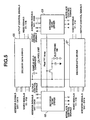
- this peripheral circuit 2B is formed of data drivers 66, 67 connected to both ends of the respective data lines of the pixel unit 2A, and scan drivers 68, 69 connected to both ends of the respective data lines of the pixel unit 2A.
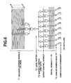
- the data drivers 66, 67 respectively comprise a 9-bit decoder 11, a level shifter 72, a buffer and AND gate switch unit 73, and an analog sample hold TFT 74.
- the decoder 71 is formed of three NAND gates, one NOR gate, and eighteen address signal lines.
- the output terminal of this decoder 71 is connected to eight buffers, and simultaneously transmits address signals to eight data lines.
- the eight analog sample hold TFTs are simultaneously switched, and eight data are simultaneously transferred to the hold condenser.
- This structure is suitable for decreasing the speed of the data drivers 66, 67.
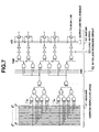
- the scan drivers 68, 69 respectively comprise a 10-bit decoder 81, an interlace exchange circuit 82, a level shifter 83 and an output buffer 84.
- This structure is illustrated with a mode for simultaneously scanning two lines, and with a non-interlace scan mode.
- the interlace exchange circuit 82 applies control signals A, B, C.
- the decoder method is employed for the data drivers 66, 67 and the scan drivers 68, 69, in the pixel unit 2A, it will suffice to only rewrite the pixels to be renewed for the display data of the electronic ink layer. The reduction of energy consumption will also be realized thereby.
- the controller 4 depicted in Fig. 2 conducts the interrupt processing shown in Fig. 8 for each fixed frame rate. Upon entering this interrupt processing, it is foremost judged as to whether the display data of the electronic ink layer 15 should be renewed or not (step S1). This judgment, for example, corresponds to when the reader conducts an operation so as to turn the page of the electronic book via the operational unit 3. When this judgment is YES, the controller 4 conducts the processing of step S2, but when this judgment is NO, it skips the processing of step S2.
- the controller 4 reads the contents of the data to be renewed from the memory 6, and orders the electronic ink layer 15 to conduct writing for each pixel pursuant to the above.
- the controller 4 selects and applies voltage (first voltage), via the decoder drivers 66-69, only to the pixel element 14 of the pixel coinciding with the renewal contents. Contents of the newly renewed data may thereby be displayed.
- the controller 4 may set the gradation (step S2A) based on the well-known pulse-surface-area modulation (for example, the thesis "TFT-LEPD with Image Uniformity by Area Ratio Gray Scale - M. Kimura et al.”
- this is structured of a plurality of sub pixels that adopt either the on state or off state of the respective pixels, and, depending on the number of sub pixels in the on state (off state), the gray scale (gradation) between white and black; for example, light gray or dark gray, is adjusted.
- Fig. 9 is a layout diagram of the pixel unit in a case of realizing four gradations with the pulse-surface-area modulation.
- Each pixel is structured of two sub pixels (91, 92), wherein the area of one is double the other.
- the four gradations can be realized (a) when two of the sub pixels (91, 92) are both off, (b) when only the sub pixel (91) with the smaller area is on, (c) when only the sub pixel (92) with the larger area is on, and (d) when the two of the sub pixels (91, 92) are both on.
- the contents to be displayed on the display surface is not limited to character information, and pictures and images may also be favorably expressed.
- step S3 the controller 4 judges whether it is of a refresh timing or not via timing with the count value of the counter.
- this refresh is a rewriting operation for maintaining data retention when the setting time capable of retaining the memory property of the electronic ink layer 15 elapses.
- the setting time of this refresh is a suitable time within the range of several minutes to several ten minutes.
- this refresh operation selectively reapplies a voltage pulse (second voltage) with a negative voltage property to the common electrode, and moves the charged particles 45 in the microcapsules 42 toward the display surface side; that is, toward the common electrode side in the example of Fig. 3 , or retains such state if the charged particles have already moved toward the display surface side.
- the refresh operation selectively applies a voltage pulse with a positive electrode property to the common electrode, and moves the charged particles 45 in the microcapsules 42 toward the side opposite to the display surface side; that is, toward the side opposite to the common electrode side in the example of Fig.
- the pixels represented in white pursuant to the charged particles 45 will continue to be represented in white, and the pixels represented in black pursuant to the liquid 44 will continue to be represented in black.
- the pixels represented in a gray scale pursuant to the pulse-surface-area modulation as the sub pixels thereof will similarly be refreshed, the gray scale representation will also be maintained.
- the timing of the refresh operation for the white color display and black color display may differ.
- the refresh operation will be conducted in an appropriate timing, as well as automatically and periodically, before the lapse of the time of several minutes to several ten minutes when the memory property will be lost.
- the memory property will be retained, and the picture quality of the display pattern will also be retained as per the initial display.
- this refresh operation will prevent troubles such as the display information becoming difficult to see or eliminated altogether, and will become preferable as a display device such as an electronic book.
- the information to be displayed with this display device is not only binary information as conventionally, and gradients between the binary information is represented by the pulse-surface-area modulation.
- the pulse-surface-area modulation it is possible to provide a display medium preferable for display information requiring fine tone.
- the structure will be of an overall compact size.
- the driver employs a decoder method capable of designating pixels to be rewritten by the combination of inputs, it is sufficient to conduct data rewriting by selectively designating the required pixels, and it is not necessary to rewrite all of the pixels of the pixel unit. It is therefore possible to significantly reduce the energy consumption required for rewriting the data of the electronic ink layer of the pixel unit.
- this electronic ink will enable the structure of a reflective display device with high contrast ratio, and, as a backlight will no longer be necessary, it is further possible to reduce energy consumption.
- the present invention is not limited to the aforementioned embodiment, and may be modified in various modes.
- a plurality of types of charged particles 45C, 45D with different electric charges are employed as the charged particles 45 to be scattered in the liquid 44 within the respective microcapsules 42.
- the time and/or value of the DC voltage to be applied to the common electrode and the respective pixel electrodes upon data rewriting is suitably changed.
- the change in the electric charge is reflected in the behavior of the speed or the like when the charged particles 45 move, and it is thereby possible to express an even finer gradient.
- FIG. 11 As a substitute to the monochrome representation of the aforementioned display information, another embodiment enables a color representation.
- This can be realized by employing a switching element depicted in Fig. 11 , for example, in place of the aforementioned switching element illustrated in Fig. 3 .
- the common electrode 13 and pixel electrode 14 are partitioned with a bank 93, and the electronic ink layer 15, with an electronic ink layer 15C for cyan, electronic bank layer 15M for magenta, and electronic bank layer 15Y for yellow as one set, is arranged on the pixel unit in a suitable pattern, the voltage application state of the electronic ink layer of the respective colors may be controlled in accordance with the display color pattern.
- an MIM Metal Insulator Metal
- This MIM is characterized in that it has a laminated structure of metal - insulation film - metal, and yields a bi-directional diode characteristic having a steep threshold value.
- a so-called simple matrix drive may be used to control the image display.
- Fig. 12 illustrates the basic structure of the passive matrix drive system.
- This passive matrix drive system sequentially selects in a pulse-like manner the scanning electrode 100 provided on one surface of the electronic ink layer 15, and then selects and applies voltage to the signal electrode (data electrode) 102 (other surface of the electronic ink layer 15) corresponding to the respective microcapsules upon selecting such scanning electrode 100.
- the total number of scanning electrodes 100 is N, it is only possible to apply voltage to a single scanning electrode 100 for 1/N the time of the screen display period. This will result in a limited resolution, but will be sufficient upon being employed in the display device 1 of the present embodiment.
- the drive systems of a generally known liquid crystal display device are applicable, and in comparison to the liquid crystal continuously driving the voltage, with the display device of the present embodiment, once voltage is applied, yielded is an advantage unavailable to liquid crystal display devices wherein the image is maintained even upon releasing the application of voltage thereafter.
- the drive system of the present embodiment may be any one of a static drive (seven segments, etc.), a passive matrix drive, or an active matrix drive.
- the display body 2 was fixed to the frame 1A of the display device 1, as shown in Fig. 13 , the display body 2 may be of a structure so as to be attachable and detachable to and from the frame 1A.
- the display body 2 is an extremely thin sheet-shaped or paper-shaped recording medium (electronic paper), and is held between the two pairs of feed rollers 104, 106 disposed in the frame 1A.
- a rectangular pore 1C is provided to the frame 1A, to which a transparent glass plate 107 is fitted therein.
- An insertion/removal slot 108 is also provided to the frame 1A so as to enable the insertion and removal of the display body 2 to and from this insertion/removal slot 108.
- a terminal unit 110 is provided at the tip in the insertion direction of the display body 2, and, by being electrically connected to the socket 112 in the frame 1A, it is connectable to the controller 4 in the frame 1A.
- This type of detachable display unit 2 will be easy to handle but not bulky, and, for instance, it would be possible for the user to only carry around the display unit 2 displaying the necessary map near one's destination.
- the periodic and automatic refresh operation will maintain the memory property of the electronic ink, prevent the deterioration of the picture quality of the display information, and provide a display device with persistency.
- the display device employing the electronic ink according to the present invention, as it will be sufficient to rewrite only the display contents of the pixel in a required minimum upon renewing the display contents, it is possible to provide a display device seeking energy conservation.
- the display device employing the electronic ink according to the present invention it is possible to provide a display device capable of displaying fine gradation with the likes of pulse-surface-area modulation.
- the present invention provides the creation of a novel technology of applying a prescribed voltage for retaining the image by maintaining the distribution state of the electrophoretic material in order to prevent the electrophoretic material of the recording medium after voltage application from scattering in the recording medium and not being able to maintain the image.
Abstract
Description
- The present invention generally relates to a display device, and particularly to a display device employing an electrophoretic liquid material referred to as electrophoretic ink which utilizes the electrophoretic phenomenon. This display device is also a storage medium known as electronic paper or an electronic sheet.
- The phenomenon of charged particles dispersed in a liquid electrophoresing by applying an electric field; in other words, electrophoretic phenomenon, is well known from conventionally. As an application of this phenomenon, known is the fact that by dispersing charged pigment particulates in a dispersed liquid colored with dye, sandwiching these between a pair of electrodes, and applying an electric field thereto, the charged particles are drawn to one of the electrodes, and there have been attempts at applying this to displays (Japanese Patent No.
900963 - Ti02 (rutile structure), for example, is used as the core of the charged particles, and polyethylene, for example, is used as the cover layer for covering this core. As the solvent, for instance, used is a solvent in which anthraquinone dye is dissolved in ethylene tetrachloride and isoparaffin. The charged particles and solvent have mutually differing colors, and, for example, the charged particles are white, and the solvent is blue, red, green or black. At least one of the electrodes is a transparent electrode.
- When an external electric field is applied to the electrophoretic ink (hereinafter simply referred to as "electronic ink") in the electrophoretic display, the charged particles move in the direction opposite to the direction of the electric field when the charged particles are negatively charged. Thereby, the one face for viewing the electronic ink; that is, the surface of the display, appears to be colored in either the color of the solvent or the color of the charged particles. Therefore, by controlling per pixel the movement of the charged particles of the electronic ink positioned in the respective pixel areas, it becomes possible to express display information such as characters; symbols and images on the display surface.
- As the relative density of the solvent and charged particles is set to be approximately the same, the charged particles are able to retain the position at the time of electric field application even after the disappearance of the electric field for a relatively long period of time (e.g., from several minutes to about twenty minutes) . Thus, low electric consumption can be expected upon being applied to a display.
- Moreover, the aforementioned EPD has an extremely wide viewing angle at ± 90 degrees, and the contrast is also high. In addition, with a typical EPD, the observers will as a result be viewing the color of the pigment or dye, and, for example, this is different than viewing the light of a fluorescent tube which is a backlight in a transparent liquid crystal display, and realizes a coloration gentle to the eyes. Cost reduction is further possible.
- In reality, however, reliability could not be secured due to the agglomeration of the aforementioned pigment particulates, and could not be put into practical use for a long time. Nevertheless, as it became apparent in recent years that reliability could be improved by filling electronic ink in microcapsules, EPDs were catapulted into the spotlight.
- As a specific display utilizing this electronic ink, known are the theses "44.3L: A Printed and Rollable Bistable Electronic Display - P. Drzaic et al., SED 98 DIGEST 1131" and "53.3: Microencapsulated Electrophoretic Rewritable Sheet" - H. Kawai et al., SID 99 DIGEST 1102".
- The former proposes a flexible display wherein a transparent conductor plate, capsuled electronic ink, patterned silver or graphite conductor layer, and insulation film layer are successively printed in this order on polyester film, and, in order to designate an address of the patterned conduction layer, a hole is provided in the insulation film layer and a lead line is provided therein. The later proposes a rewritable sheet pursuant to electrophoresis employing microcapsuled electronic ink, and a method for writing on this sheet.
- Nonetheless, the aforementioned EPDs still have the following unresolved problems. In other words, with electronic ink as described above, the relative density of the solvent and charged particles is set to be approximately the same, and the charged particles are thereby able to retain the position at the time of electric field application even after the disappearance of the electric field for a relatively long period of time. That is, although it possesses a retention property capable of functioning as a memory for retaining data, the time thereof is merely several minutes to several ten minutes. Thereafter, the position of the charged particles moves in the solvent, and the picture quality of the display pattern gradually deteriorates.
- Moreover, for instance, with the likes of a liquid crystal display, regardless of the screen changing or not, rewriting is conducted at a speed of sixty times per second. Upon employing this driving method, however, it is not possible to make the best use of the retention property in the aforementioned electronic ink, and low energy consumption cannot be realized thereby.
- Further, information represented by the electronic ink is basically two values (two values pursuant to whether the color appearing on the display surface by the charged particles moving is of the charged particles or the solvent), and a fine gradation cannot yet be expressed in a sufficient manner.
- Accordingly, an object of the present invention is to retain the function of maintaining information displayed by the electronic ink and preventing the deterioration of the picture quality of the display information in a display device using the electrophoretic phenomenon of a liquid material.
- Another object of the present invention is to enable the rewriting of display contents of pixels to be of a required minimum upon renewing the display contents and realizing low energy consumption in this type of display device.
- A further object of the present invention is to enable the expression of fine gradation in this type of display device.
- In order to achieve the foregoing objects, the present invention is a display device in which the display state is prescribed by the distribution state of particles, comprising a drive circuit for applying a first voltage for changing the distribution state of the particles, and for applying a second voltage for maintaining the distribution state of the particles.
- In the present invention, the maintenance of the distribution state will suffice so as long as it is within the permissible deflection for obtaining a desired display precision; in other words, the distribution position of charged particles does not have to be completely secured so as long as the distribution state of particles can be substantially maintained. For instance, the charged particles are contained in a microcapsule together with liquid for dispersing such charged particles. The charged particles may be of a single type, or a mixture of a plurality of types, and may also be of a composite structure to be contained in a microcapsule.
- The present invention is further characterized in that it is provided with a plurality of scanning electrodes and a plurality of data electrodes disposed so as to sandwich the charged particles and for applying voltage to the charged particles. This structure corresponds to the so-called passive voltage application drive system.
- The present invention is further characterized in that the aforementioned particles are divided into a plurality of areas, and that it is provided with a plurality of scanning lines and a plurality of data lines for applying voltage independently in such divided areas. This is the so-called active voltage application drive system, and, for example, is structured such that the pixels are disposed in an array, and a switching element, which is an active element, is disposed at the each intersection of the plurality of scanning lines and plurality of data lines. A semiconductor element may be employed as the switching element, and the semiconductor element is principally a thin film transistor. Another example of the switching element is a two-terminal nonlinear element.
- In order to achieve the aforementioned objects, the present invention is a display device comprising a data writing circuit which moves charged particles and writes data by filling liquid having charged particles dispersed therein between an active matrix substrate, in which switching elements and pixel electrodes disposed in correspondence with the switching elements are arranged in an array, and an opposed substrate, and applying voltage for each pixel between the active matrix substrate and the opposed substrate; wherein the display device further comprises a refresh circuit for refreshing at prescribed intervals the data of each pixel written pursuant to the data writing circuit.
- In order to achieve the foregoing objects, the present invention is a display device comprising a data writing circuit which moves charged particles and writes data by disposing a microcapsule filled with liquid having charged particles dispersed therein between an active matrix substrate, in which switching elements and pixel electrodes disposed in correspondence with the switching elements are arranged in an array, and an opposed substrate, and applying voltage for each pixel between the active matrix substrate and the opposed substrate; wherein the display device further comprises a refresh circuit for refreshing at prescribed intervals the data of each pixel written pursuant to the data writing circuit.
- In order to achieve the aforementioned objects, the present invention is a display device comprising a data writing circuit which moves charged particles and writes data by filling liquid having charged particles dispersed therein between an active matrix substrate, in which switching elements and pixel electrodes disposed in correspondence with the switching elements are arranged in an array, and an opposed substrate, and applying voltage for each pixel between the active matrix substrate and the opposed substrate; wherein the data writing circuit comprises a switch for turning the data writing on/off and structured of the switching elements and a driver for controlling the switching elements, and the driver is structured so as to be driven with a decoder method.
- Here, the driver for controlling the switching element shall mean a data driver to be connected to the data line and a scan driver to be connected to the scan line of the pixel unit in many cases. The writing of data will realize low energy consumption by selecting and rewriting only the pixels for rewriting data.
- In order to achieve the foregoing objects, the present invention is a display device comprising a data writing circuit which moves charged particles and writes data by disposing a microcapsule filled with liquid having charged particles dispersed therein between an active matrix substrate, in which switching elements and pixel electrodes disposed in correspondence with the switching elements are arranged in an array, and an opposed substrate, and applying voltage for each pixel between the active matrix substrate and the opposed substrate; wherein the data writing circuit comprises a switch for turning the data writing on/off and structured of the switching elements and a driver for controlling the switching elements, and the driver is structured so as to be driven with a decoder method.
- Here, the driver for controlling the switching element shall mean a data driver to be connected to the data line and a scan driver to be connected to the scan line of the pixel unit in many cases. The writing of data will realize low energy consumption by selecting and rewriting only the pixels for rewriting data.
- In order to achieve the aforementioned objects, the present invention is a display device comprising a data writing circuit which moves charged particles and writes data by filling liquid having charged particles dispersed therein between an active matrix substrate, in which switching elements and pixel electrodes disposed in correspondence with the switching elements are arranged in an array, and an opposed substrate, and applying voltage for each pixel between the active matrix substrate and the opposed substrate; wherein a single pixel is structured of a plurality of sub pixels, and gradation is controlled by pulse-surface-area modulation.
- In order to achieve the foregoing objects, the present invention is a display device comprising a data writing circuit which moves charged particles and writes data by disposing a microcapsule filled with liquid having charged particles dispersed therein between an active matrix substrate, in which switching elements and pixel electrodes disposed in correspondence with the switching elements are arranged in an array, and an opposed substrate, and applying voltage for each pixel between the active matrix substrate and the opposed substrate; wherein a single pixel is structured of a plurality of sub pixels, and gradation is controlled by pulse-surface-area modulation.
- In order to achieve the aforementioned objects, the present invention is a display device comprising a data writing circuit which moves charged particles and writes data by filling liquid having charged particles dispersed therein between an active matrix substrate, in which switching elements and pixel electrodes disposed in correspondence with the switching elements are arranged in an array, and an opposed substrate, and applying voltage for each pixel between the active matrix substrate and the opposed substrate; wherein the charged particles are formed of a plurality of types of charged particles with differing quantities of electric charge.
- In the present invention, the gradient is controlled by controlling one or both of the value/time of the voltage to be applied with the data writing circuit.
- In order to achieve the foregoing objects, the present invention is a display device comprising a data writing circuit which moves charged particles and writes data by disposing a microcapsule filled with liquid having charged particles dispersed therein between an active matrix substrate, in which switching elements and pixel electrodes disposed in correspondence with the switching elements are arranged in an array, and an opposed substrate, and applying voltage for each pixel between the active matrix substrate and the opposed substrate; wherein the charged particles are formed of a plurality of types of charged particles with differing quantities of electric charge.
- In the present invention, the gradient is controlled by controlling one or both of the value/time of the voltage to be applied with the data writing circuit.
- In the present invention, it is preferable that the switching element is a low-temperature poly-Si TFT as the switching element has high mobility, and as it is possible to integrate a driver. Moreover, from the perspective of cost reduction, it is preferable that the switching element is a TFT of a structure wherein the channel portion is at least formed of an organic film.
- In the present invention, the refresh circuit does not necessarily once clear (delete) the data of images and characters generating the distribution of the charged particles. In other words, with the display device of the present invention, voltage is applied upon initially displaying the image, and, thereafter, the relative density of the particles and liquid is approximately the same, and the distribution state of charged particles can be maintained even when the application of voltage is released. In this type of display device, with the purpose of stabilizing or maintaining the initial distribution state of charged particles upon having applied voltage to charged particles, voltage merely needs to be applied periodically or occasionally based on the image data. That is, different from the "refresh" implying the deletion and writing of data conducted conventionally with liquid crystal displays, it is not necessarily imperative to delete the data in the present invention. As the display device of the present invention also functions as electronic paper; in other words, since it comprises a function of displaying image and character information as is in correspondence to the distribution of charged particles for a prescribed period of time after applying voltage to the charged particles in accordance with image data, the present invention also corresponds to a recording medium. With the display device structured of at least a display unit, which is the recording medium, and peripheral circuits containing the voltage application circuit, for example, even upon removing the display unit from the peripheral circuit, it would still be possible for users to confirm the information displayed on this electronic paper at home, in the office, and so on. Further, for instance, upon employing the present invention in a car navigation system, it would be possible for a user to remove the portion (electronic paper) displaying the map upon having arrived at a parking space nearby one's destination from the peripheral circuit, and bring it along while he/she walks to the destination.
-
-
Fig. 1 is a diagram showing the appearance of an electronic book as the display device employing the present invention; -
Fig. 2 is a diagram showing the electric block structure of the display device; -
Fig. 3 is a partial cross section of a switching element forming the pixel unit of the display body of the display device; -
Fig. 4 is a diagram explaining the schematic structure of the electronic ink layer and the operation thereof upon application of voltage; -
Fig. 5 is a block diagram showing the schematic structure of the display body of the display device; -
Fig. 6 is a block diagram showing the schematic structure of a decoder data driver as the peripheral circuit of the pixel unit; -
Fig. 7 is a block diagram showing the schematic structure of a decoder scan driver as the peripheral circuit of the pixel unit; -
Fig. 8 is a schematic flowchart explaining the renew and refresh operations of the display data with a controller; -
Fig. 9 is a layout diagram of the pixel unit upon realizing four gradations with pulse-surface-area modulation; -
Fig. 10 is a conceptual diagram of a microcapsule containing charged particles having different electric charge and pertaining to a modified example of the electronic ink layer; -
Fig. 11 is a partial cross section showing a color thin-film structure pertaining to a modified example of the switching element; -
Fig. 12 is a schematic diagram of a passive driving method in the display device of the present invention; and -
Fig. 13 is a side view of the display device having a detachable display body (electronic paper/recording medium) . - Embodiments of the present invention are now explained with reference to the attached drawings. The
display device 1 according to the present embodiment has, for example, a shape of an electronic book (sometimes referred to as "electronic paper") as shown inFig. 1 . Thisdisplay device 1 comprises a book-shapedframe 1A, and a cover B1 for opening and closing thisframe 1A. Adisplay body 2 is provided on the surface of theframe 1A in a state where the display surface thereof is exposed, and anoperational unit 3 is also provided thereto.Frame 1A has a built-incontroller 4, acounter 5 and a memory 6 (refer toFig. 2 ). - The
display body 2 of the present embodiment comprises apixel unit 2A formed by filling electronic ink in a switching element, and aperipheral circuit 2B provided integrally with thispixel unit 2A. As described later, theperipheral circuit 2B comprises a decoder-type scan driver and data driver. -
Fig. 3 shows a cross section structure of thepixel unit 2A. As shown inFig. 3 , anopposed substrate 12 is adhered on thesubstrate 11, and acommon electrode 13 is formed on thisopposed substrate 12. Anelectronic ink layer 15 is laminated between thiscommon electrode 13 and apixel element 14. Thispixel element 14 is serially connected to adrain electrode 17 of aTFT 16, and this TFT acts as a switch. Here, either thecommon electrode 13 or thepixel electrode 14 is of a transparent electrode, and the transparent electrode side will become the display surface. - The TFT comprises a
source layer 19, achannel 20 and adrain layer 21 formed on thebase insulation film 18; agate insulation film 22 formed thereon; agate electrode 23 formed on thisgate insulation film 22; asource electrode 24 formed on thesource layer 19; and adrain electrode 17 formed on thedrain layer 21. The TFT is further sequentially covered with aninsulation film 25 and aninsulation film 26. - As shown in
Fig. 4 , theelectronic ink layer 15 is structured of atransparent binder 41 having optical permeability, and a plurality ofmicrocapsules 42 dispersed uniformly and fixedly in thisbinder 41. The thickness of theelectronic ink layer 15 is approximately 1.5 to 2 times the diameter of themicrocapsule 42. Silicon resin or the like is used as the material of thebinder 41. Themicrocapsule 42 comprises a hollow andspherical capsule body 43 having optical permeability. Liquid (solvent) 44 is filled in thiscapsule body 43, and a plurality of electronegative chargedparticles 45 are dispersed in the liquid 44. Each of the chargedparticles 45 is structured of acore 45A, and acover layer 45B for covering such core. The color of the chargedparticle 45 andliquid 44 is set to be mutually different. As an example, the charged particle may be white, while the liquid may be blue, red, green or black. The relative density of the liquid 44 and the chargedparticles 45 is set to be of a mutually and substantially equivalent value in therespective microcapsules 42. - When an electric field is applied externally to the microcapsules in the aforementioned state, the charged
particles 45 move in a direction opposite to the direction of the electric field in themicrocapsules 42. As a result, presuming that the current display surface is on the upper side face (i.e., surface of the opposed substrate side) ofFig. 3 , when the chargedparticles 45 move toward the upper side inFig. 3 , viewed will be the color (white for example) of the chargedparticles 45 standing out with the color (blue, red, green or black for example) of the liquid 44 being the background (refer toFig. 4 (B) ) . Contrarily, when the chargedparticles 45 move toward the lower side inFig. 3 pursuant to the application of the electric field, only the color (blue, red, green or black for example) of the liquid 44 can be viewed (refer toFig. 4(C) ). - The charged
particles 45 that moved toward the direction opposite to the direction of the electric field pursuant to the application of such electric field have a relative density approximately the same as with the liquid 44, and, therefore, try to stay at such position for a long period of time even after the electric field is eliminated. In other words, they have a retention property (a property capable of being used as a memory, hereinafter referred to "memory property"), and the color of the chargedparticles 45 or liquid 44 appearing on the display surface is retained for an interim (several minutes to several ten minutes). Here, by controlling the application of the electric field for each pixel, information according to such application pattern will be displayed on the display surface (refer toFig. 1 ) of thedisplay body 2, and such information will be retained for a relatively long period of time. - Nevertheless, pursuant to the lapse in time, the charged
particles 45 naturally diffuse as a result of gravity and vibration, the picture quality of the display surface presenting the information will gradually deteriorate, and information can no longer be accurately displayed. Thus, in the present embodiment, as described later, the refresh operation is periodically implemented in order to maintain the presentation of the information. - Moreover, information pursuant to the movement of charged
particles 45 by the electric field will only be binary information to be presented at this rate. In other words, information to be decided by whether the color appearing on the display screen is pursuant to the charged particles 45 (white for example), or pursuant to the liquid 44 (black for example). The present embodiment therefore proposes the realization of gradation (gray scale) with a method referred to as pulse-surface-area modulation - The
peripheral circuit 2B uniformly and integrally formed with thepixel unit 2A and forming thedisplay body 2 is now explained with reference toFigs. 5 to 7 . As shown inFig. 5 , thisperipheral circuit 2B is formed ofdata drivers pixel unit 2A, and scandrivers pixel unit 2A. As shown inFig. 6 , thedata drivers bit decoder 11, alevel shifter 72, a buffer and AND gate switch unit 73, and an analog sample holdTFT 74. Thedecoder 71 is formed of three NAND gates, one NOR gate, and eighteen address signal lines. The output terminal of thisdecoder 71 is connected to eight buffers, and simultaneously transmits address signals to eight data lines. Thus, the eight analog sample hold TFTs are simultaneously switched, and eight data are simultaneously transferred to the hold condenser. This structure is suitable for decreasing the speed of thedata drivers - Meanwhile, as shown in
Fig. 7 , thescan drivers bit decoder 81, an interlace exchange circuit 82, alevel shifter 83 and anoutput buffer 84. This structure is illustrated with a mode for simultaneously scanning two lines, and with a non-interlace scan mode. In order to scan with these scan modes, a structure is adopted wherein the interlace exchange circuit 82 applies control signals A, B, C. By simultaneously scanning two lines as described above, it is possible to increase the resolution in the vertical direction without having to increase the scan rate. A pair of scan lines is simultaneously selected, and this combination is exchanged between the two conditions. - As described above, since the decoder method is employed for the
data drivers scan drivers pixel unit 2A, it will suffice to only rewrite the pixels to be renewed for the display data of the electronic ink layer. The reduction of energy consumption will also be realized thereby. - Here, let it be assumed that when a pulse, which is a negative electrode against the
common electrode 13 and of a prescribed voltage value, is applied to thepixel electrode 14, the white color of the chargedparticles 45 in themicrocapsules 42 appears on the display surface, and, meanwhile, when a pulse, which is a positive electrode against thecommon electrode 13 and of a prescribed voltage value, is applied to thepixel electrode 14, the black color of the liquid 45 appears on the display surface. - The
controller 4 depicted inFig. 2 conducts the interrupt processing shown inFig. 8 for each fixed frame rate. Upon entering this interrupt processing, it is foremost judged as to whether the display data of theelectronic ink layer 15 should be renewed or not (step S1). This judgment, for example, corresponds to when the reader conducts an operation so as to turn the page of the electronic book via theoperational unit 3. When this judgment is YES, thecontroller 4 conducts the processing of step S2, but when this judgment is NO, it skips the processing of step S2. - At step S2, the
controller 4 reads the contents of the data to be renewed from thememory 6, and orders theelectronic ink layer 15 to conduct writing for each pixel pursuant to the above. - In such a case, the
controller 4 selects and applies voltage (first voltage), via the decoder drivers 66-69, only to thepixel element 14 of the pixel coinciding with the renewal contents. Contents of the newly renewed data may thereby be displayed. - In this data renewal processing, the
controller 4 may set the gradation (step S2A) based on the well-known pulse-surface-area modulation (for example, the thesis "TFT-LEPD with Image Uniformity by Area Ratio Gray Scale - M. Kimura et al." In other words, this is structured of a plurality of sub pixels that adopt either the on state or off state of the respective pixels, and, depending on the number of sub pixels in the on state (off state), the gray scale (gradation) between white and black; for example, light gray or dark gray, is adjusted. For instance,Fig. 9 is a layout diagram of the pixel unit in a case of realizing four gradations with the pulse-surface-area modulation. Each pixel is structured of two sub pixels (91, 92), wherein the area of one is double the other. Here, the four gradations can be realized (a) when two of the sub pixels (91, 92) are both off, (b) when only the sub pixel (91) with the smaller area is on, (c) when only the sub pixel (92) with the larger area is on, and (d) when the two of the sub pixels (91, 92) are both on. Thereby, the contents to be displayed on the display surface is not limited to character information, and pictures and images may also be favorably expressed. - Next, the
controller 4 judges whether it is of a refresh timing or not via timing with the count value of the counter (step S3). As described above, this refresh is a rewriting operation for maintaining data retention when the setting time capable of retaining the memory property of theelectronic ink layer 15 elapses. The setting time of this refresh is a suitable time within the range of several minutes to several ten minutes. When the judgment at this step S3 is NO; that is, when the refresh timing has not yet been reached, the processing at the next step S4 is skipped. Contrarily, when the judgment at step S3 is YES, the refresh operation is ordered (step S4). - With respect to the pixels displaying white for example, this refresh operation selectively reapplies a voltage pulse (second voltage) with a negative voltage property to the common electrode, and moves the charged
particles 45 in themicrocapsules 42 toward the display surface side; that is, toward the common electrode side in the example ofFig. 3 , or retains such state if the charged particles have already moved toward the display surface side. Then, regarding the pixels displaying black, the refresh operation selectively applies a voltage pulse with a positive electrode property to the common electrode, and moves the chargedparticles 45 in themicrocapsules 42 toward the side opposite to the display surface side; that is, toward the side opposite to the common electrode side in the example ofFig. 3 , or retains such state if the charged particles have already moved toward the side opposite to the display surface side. Thereby, prior to the refresh operation, the pixels represented in white pursuant to the chargedparticles 45 will continue to be represented in white, and the pixels represented in black pursuant to the liquid 44 will continue to be represented in black. Here, regarding the pixels represented in a gray scale pursuant to the pulse-surface-area modulation, as the sub pixels thereof will similarly be refreshed, the gray scale representation will also be maintained. Moreover, with respect to the aforementioned example, the timing of the refresh operation for the white color display and black color display may differ. - The aforementioned processing will be repeatedly executed in prescribed intervals. According to the display of the present embodiment, unlike the display body employing conventional electronic ink, the refresh operation will be conducted in an appropriate timing, as well as automatically and periodically, before the lapse of the time of several minutes to several ten minutes when the memory property will be lost. Thus, the memory property will be retained, and the picture quality of the display pattern will also be retained as per the initial display. In other words, this refresh operation will prevent troubles such as the display information becoming difficult to see or eliminated altogether, and will become preferable as a display device such as an electronic book.
- Furthermore, the information to be displayed with this display device is not only binary information as conventionally, and gradients between the binary information is represented by the pulse-surface-area modulation. Thus, it is possible to provide a display medium preferable for display information requiring fine tone.
- In addition, as the peripheral driver is uniformly and integrally manufactured with the switching element, the structure will be of an overall compact size.
- Moreover, as the driver employs a decoder method capable of designating pixels to be rewritten by the combination of inputs, it is sufficient to conduct data rewriting by selectively designating the required pixels, and it is not necessary to rewrite all of the pixels of the pixel unit. It is therefore possible to significantly reduce the energy consumption required for rewriting the data of the electronic ink layer of the pixel unit.
- Further, the employment of this electronic ink will enable the structure of a reflective display device with high contrast ratio, and, as a backlight will no longer be necessary, it is further possible to reduce energy consumption.
- The present invention is not limited to the aforementioned embodiment, and may be modified in various modes.
- As one mode thereof, wherein the conceptual structure is shown in
Fig. 10 , a plurality of types of chargedparticles particle 45D is twice that of the other chargedparticle 45C) are employed as the chargedparticles 45 to be scattered in the liquid 44 within therespective microcapsules 42. Then, the time and/or value of the DC voltage to be applied to the common electrode and the respective pixel electrodes upon data rewriting is suitably changed. The change in the electric charge is reflected in the behavior of the speed or the like when the chargedparticles 45 move, and it is thereby possible to express an even finer gradient. - As a substitute to the monochrome representation of the aforementioned display information, another embodiment enables a color representation. This can be realized by employing a switching element depicted in
Fig. 11 , for example, in place of the aforementioned switching element illustrated inFig. 3 . Specifically, by adopting a structure wherein thecommon electrode 13 andpixel electrode 14 are partitioned with abank 93, and theelectronic ink layer 15, with anelectronic ink layer 15C for cyan, electronic bank layer 15M for magenta, andelectronic bank layer 15Y for yellow as one set, is arranged on the pixel unit in a suitable pattern, the voltage application state of the electronic ink layer of the respective colors may be controlled in accordance with the display color pattern. - Further, with the aforementioned embodiment, although a TFT element was employed as the switching element being the mainstream of the so-called active matrix drive, an MIM (Metal Insulator Metal) element may also be used. This MIM is characterized in that it has a laminated structure of metal - insulation film - metal, and yields a bi-directional diode characteristic having a steep threshold value.
- Moreover, without limitation to the foregoing active matrix drive, a so-called simple matrix drive (passive matrix drive) may be used to control the image display.
-
Fig. 12 illustrates the basic structure of the passive matrix drive system. This passive matrix drive system sequentially selects in a pulse-like manner thescanning electrode 100 provided on one surface of theelectronic ink layer 15, and then selects and applies voltage to the signal electrode (data electrode) 102 (other surface of the electronic ink layer 15) corresponding to the respective microcapsules upon selectingsuch scanning electrode 100. Presuming that the total number ofscanning electrodes 100 is N, it is only possible to apply voltage to asingle scanning electrode 100 for 1/N the time of the screen display period. This will result in a limited resolution, but will be sufficient upon being employed in thedisplay device 1 of the present embodiment. In other words, the drive systems of a generally known liquid crystal display device are applicable, and in comparison to the liquid crystal continuously driving the voltage, with the display device of the present embodiment, once voltage is applied, yielded is an advantage unavailable to liquid crystal display devices wherein the image is maintained even upon releasing the application of voltage thereafter. - Therefore, the drive system of the present embodiment may be any one of a static drive (seven segments, etc.), a passive matrix drive, or an active matrix drive.
- Moreover, although the
display body 2 was fixed to theframe 1A of thedisplay device 1, as shown inFig. 13 , thedisplay body 2 may be of a structure so as to be attachable and detachable to and from theframe 1A. Thedisplay body 2 is an extremely thin sheet-shaped or paper-shaped recording medium (electronic paper), and is held between the two pairs offeed rollers frame 1A. Arectangular pore 1C is provided to theframe 1A, to which atransparent glass plate 107 is fitted therein. An insertion/removal slot 108 is also provided to theframe 1A so as to enable the insertion and removal of thedisplay body 2 to and from this insertion/removal slot 108. Aterminal unit 110 is provided at the tip in the insertion direction of thedisplay body 2, and, by being electrically connected to thesocket 112 in theframe 1A, it is connectable to thecontroller 4 in theframe 1A. - This type of
detachable display unit 2 will be easy to handle but not bulky, and, for instance, it would be possible for the user to only carry around thedisplay unit 2 displaying the necessary map near one's destination. - As described above, according to the present invention, the periodic and automatic refresh operation will maintain the memory property of the electronic ink, prevent the deterioration of the picture quality of the display information, and provide a display device with persistency.
- With the display device employing the electronic ink according to the present invention, as it will be sufficient to rewrite only the display contents of the pixel in a required minimum upon renewing the display contents, it is possible to provide a display device seeking energy conservation.
- Moreover, with the display device employing the electronic ink according to the present invention, it is possible to provide a display device capable of displaying fine gradation with the likes of pulse-surface-area modulation.
- Furthermore, the present invention provides the creation of a novel technology of applying a prescribed voltage for retaining the image by maintaining the distribution state of the electrophoretic material in order to prevent the electrophoretic material of the recording medium after voltage application from scattering in the recording medium and not being able to maintain the image.
Claims (4)
- A circuit which is adapted to control a first display state and a second display state of a pixel of an electrophoretic display device (2), the pixel including a plurality of charged particles (45), the circuit comprising:a controller (4) adapted to apply, at a first interval, a first electric field of a first polarity to the pixel in order to move at least a part of the plurality of charged particles (45) to a first distribution state, the controller (4) being further adapted to automatically apply, at a second interval, a second electric field of a second polarity to the pixel after the first interval in order to move the at least a part of the plurality of charged particles (45) to a second distribution state, the first and second intervals being different from each other.
- The circuit according to claim 1, further comprising:a counter (5) adapted to supply a count value to the controller (4), the count value measuring the first interval.
- The circuit according to claim 1 or 2, further comprising:a memory (6) which is electrically connected to the controller (4).
- A display device (2), comprising:a pixel region; andthe circuit according to any one of claims 1 to 3.
Applications Claiming Priority (2)
| Application Number | Priority Date | Filing Date | Title |
|---|---|---|---|
| JP2000157050 | 2000-05-26 | ||
| EP01932296A EP1286326B1 (en) | 2000-05-26 | 2001-05-28 | Display and recorded medium |
Related Parent Applications (1)
| Application Number | Title | Priority Date | Filing Date |
|---|---|---|---|
| EP01932296A Division EP1286326B1 (en) | 2000-05-26 | 2001-05-28 | Display and recorded medium |
Publications (1)
| Publication Number | Publication Date |
|---|---|
| EP1947505A1 true EP1947505A1 (en) | 2008-07-23 |
Family
ID=18661749
Family Applications (2)
| Application Number | Title | Priority Date | Filing Date |
|---|---|---|---|
| EP08075307A Withdrawn EP1947505A1 (en) | 2000-05-26 | 2001-05-28 | Display device and recording medium |
| EP01932296A Expired - Lifetime EP1286326B1 (en) | 2000-05-26 | 2001-05-28 | Display and recorded medium |
Family Applications After (1)
| Application Number | Title | Priority Date | Filing Date |
|---|---|---|---|
| EP01932296A Expired - Lifetime EP1286326B1 (en) | 2000-05-26 | 2001-05-28 | Display and recorded medium |
Country Status (5)
| Country | Link |
|---|---|
| US (1) | US6842165B2 (en) |
| EP (2) | EP1947505A1 (en) |
| CN (1) | CN1197044C (en) |
| DE (1) | DE60139393D1 (en) |
| WO (1) | WO2001091096A1 (en) |
Cited By (2)
| Publication number | Priority date | Publication date | Assignee | Title |
|---|---|---|---|---|
| US8599469B2 (en) | 2002-03-14 | 2013-12-03 | Semiconductor Energy Laboratory Co., Ltd. | Display device and method of fabricating the same |
| US9397117B2 (en) | 2009-05-02 | 2016-07-19 | Semiconductor Energy Laboratory Co., Ltd. | Display device |
Families Citing this family (99)
| Publication number | Priority date | Publication date | Assignee | Title |
|---|---|---|---|---|
| US7193625B2 (en) | 1999-04-30 | 2007-03-20 | E Ink Corporation | Methods for driving electro-optic displays, and apparatus for use therein |
| US8115729B2 (en) | 1999-05-03 | 2012-02-14 | E Ink Corporation | Electrophoretic display element with filler particles |
| US7038655B2 (en) * | 1999-05-03 | 2006-05-02 | E Ink Corporation | Electrophoretic ink composed of particles with field dependent mobilities |
| JP4613727B2 (en) * | 2000-06-22 | 2011-01-19 | セイコーエプソン株式会社 | Electrophoretic display device driving method, driving circuit, electrophoretic display device, and electronic apparatus |
| JP4557068B2 (en) * | 2000-06-22 | 2010-10-06 | セイコーエプソン株式会社 | Electrophoretic display device driving method, driving circuit, electrophoretic display device, and electronic apparatus |
| US6762744B2 (en) * | 2000-06-22 | 2004-07-13 | Seiko Epson Corporation | Method and circuit for driving electrophoretic display, electrophoretic display and electronic device using same |
| JP3719172B2 (en) * | 2000-08-31 | 2005-11-24 | セイコーエプソン株式会社 | Display device and electronic device |
| JP4134543B2 (en) * | 2001-06-26 | 2008-08-20 | 富士ゼロックス株式会社 | Image display device and display driving method |
| TW550529B (en) * | 2001-08-17 | 2003-09-01 | Sipix Imaging Inc | An improved electrophoretic display with dual-mode switching |
| US7492505B2 (en) | 2001-08-17 | 2009-02-17 | Sipix Imaging, Inc. | Electrophoretic display with dual mode switching |
| US7038670B2 (en) * | 2002-08-16 | 2006-05-02 | Sipix Imaging, Inc. | Electrophoretic display with dual mode switching |
| JP4785300B2 (en) * | 2001-09-07 | 2011-10-05 | 株式会社半導体エネルギー研究所 | Electrophoretic display device, display device, and electronic device |
| US20030071780A1 (en) * | 2001-10-16 | 2003-04-17 | Vincent Kent D. | High resolution display |
| JP2003216111A (en) * | 2002-01-28 | 2003-07-30 | Sharp Corp | Device and system of display |
| WO2003075086A2 (en) * | 2002-03-05 | 2003-09-12 | Koninklijke Philips Electronics N.V. | Electrophoretic display device and driving means for restoring the brightness level |
| US20030214475A1 (en) * | 2002-05-17 | 2003-11-20 | Sharp Kabushiki Kaisha | Display medium |
| US7043014B2 (en) * | 2002-05-22 | 2006-05-09 | Avaya Technology Corp. | Apparatus and method for time-alignment of two signals |
| US20080024482A1 (en) * | 2002-06-13 | 2008-01-31 | E Ink Corporation | Methods for driving electro-optic displays |
| JP4651383B2 (en) * | 2002-06-13 | 2011-03-16 | イー インク コーポレイション | Method for driving electro-optic display device |
| CN101800034B (en) * | 2002-06-13 | 2013-03-06 | 伊英克公司 | Method for addressing bistable electro-optical medium |
| JP2004030365A (en) * | 2002-06-27 | 2004-01-29 | Nippon Signal Co Ltd:The | Information display card |
| JP2005531801A (en) * | 2002-07-01 | 2005-10-20 | コーニンクレッカ フィリップス エレクトロニクス エヌ ヴィ | Electrophoretic display panel |
| US7038656B2 (en) * | 2002-08-16 | 2006-05-02 | Sipix Imaging, Inc. | Electrophoretic display with dual-mode switching |
| US7271947B2 (en) * | 2002-08-16 | 2007-09-18 | Sipix Imaging, Inc. | Electrophoretic display with dual-mode switching |
| JP4196615B2 (en) * | 2002-08-22 | 2008-12-17 | セイコーエプソン株式会社 | Electro-optical device, driving method of electro-optical device, and electronic apparatus |
| JP4325164B2 (en) * | 2002-09-11 | 2009-09-02 | セイコーエプソン株式会社 | Electro-optical device, driving method of electro-optical device, and electronic apparatus |
| US6877659B2 (en) * | 2002-10-04 | 2005-04-12 | Xerox Corporation | Gyricon platen cover for show-through correction |
| US20130063333A1 (en) | 2002-10-16 | 2013-03-14 | E Ink Corporation | Electrophoretic displays |
| JP4947901B2 (en) * | 2002-10-16 | 2012-06-06 | アドレア エルエルシー | Display device having a display device having a DC balancing circuit |
| KR100503413B1 (en) * | 2002-10-31 | 2005-07-22 | 한국전자통신연구원 | Template type electrophoretic display and manufacturing method thereof |
| KR20050092779A (en) * | 2003-01-23 | 2005-09-22 | 코닌클리케 필립스 일렉트로닉스 엔.브이. | Driving a bi-stable matrix display device |
| EP1629455A1 (en) * | 2003-05-23 | 2006-03-01 | Koninklijke Philips Electronics N.V. | An improved driving scheme for an electrophoretic display |
| EP1484737A1 (en) * | 2003-06-05 | 2004-12-08 | ARM Limited | Display controller |
| CN101882423B (en) * | 2003-06-30 | 2014-02-12 | 伊英克公司 | Methods for driving electro-optic displays |
| CN1820299A (en) * | 2003-07-11 | 2006-08-16 | 皇家飞利浦电子股份有限公司 | Electrophoretic display unit |
| US20060158572A1 (en) * | 2003-07-11 | 2006-07-20 | Guofu Zhou | Electrophoretic display unit |
| TW200511178A (en) * | 2003-08-25 | 2005-03-16 | Koninkl Philips Electronics Nv | Method of compensating image instability and improving greyscale accuracy for electrophoretic displays |
| CN101419779B (en) * | 2003-10-08 | 2011-03-30 | 皇家飞利浦电子股份有限公司 | Electrowetting display device |
| JP4599049B2 (en) * | 2003-11-06 | 2010-12-15 | ローム株式会社 | Display device and portable device using the same |
| KR100565196B1 (en) * | 2003-11-17 | 2006-03-30 | 엘지전자 주식회사 | Apparatus and method for driving electronic ink display panel |
| US8928562B2 (en) * | 2003-11-25 | 2015-01-06 | E Ink Corporation | Electro-optic displays, and methods for driving same |
| CN100430986C (en) * | 2003-11-26 | 2008-11-05 | 伊英克公司 | Electro-optic displays with reduced remnant voltage |
| WO2005059876A2 (en) * | 2003-12-17 | 2005-06-30 | Koninklijke Philips Electronics, N.V. | Embedded location codes for e-brush position determination |
| TW200625223A (en) * | 2004-04-13 | 2006-07-16 | Koninkl Philips Electronics Nv | Electrophoretic display with rapid drawing mode waveform |
| US20050261046A1 (en) * | 2004-05-19 | 2005-11-24 | Chan Griswold | Electronic inserts for a gaming apparatus |
| JP4649890B2 (en) * | 2004-06-29 | 2011-03-16 | 富士ゼロックス株式会社 | Driving device for image display medium |
| US11250794B2 (en) | 2004-07-27 | 2022-02-15 | E Ink Corporation | Methods for driving electrophoretic displays using dielectrophoretic forces |
| US20060083694A1 (en) | 2004-08-07 | 2006-04-20 | Cabot Corporation | Multi-component particles comprising inorganic nanoparticles distributed in an organic matrix and processes for making and using same |
| EP1780591A4 (en) * | 2004-08-20 | 2009-07-29 | Bridgestone Corp | Information display system |
| KR20060090076A (en) * | 2005-02-07 | 2006-08-10 | 삼성전자주식회사 | Display device and method for driving thereof |
| JP4718859B2 (en) * | 2005-02-17 | 2011-07-06 | セイコーエプソン株式会社 | Electrophoresis apparatus, driving method thereof, and electronic apparatus |
| JP4692020B2 (en) * | 2005-02-24 | 2011-06-01 | 富士ゼロックス株式会社 | Image display device |
| CN101373580B (en) * | 2005-03-29 | 2011-02-02 | 精工爱普生株式会社 | Method for driving electrophoretic display device |
| US7748748B2 (en) | 2005-04-12 | 2010-07-06 | International Business Machines Corporation | Method and system for generating and authenticating documents having stored electrostatic pattern information |
| TW200731180A (en) * | 2006-02-08 | 2007-08-16 | Lite On Technology Corp | Device with electrically alterable exterior |
| JPWO2007099829A1 (en) * | 2006-02-22 | 2009-07-16 | 株式会社ブリヂストン | Information equipment |
| TW200732808A (en) * | 2006-02-24 | 2007-09-01 | Prime View Int Co Ltd | Thin film transistor array substrate and electronic ink display device |
| KR100748358B1 (en) * | 2006-08-08 | 2007-08-09 | 삼성에스디아이 주식회사 | Logic gate, scan driver and organic light emitting display using the same |
| KR101363835B1 (en) * | 2007-02-05 | 2014-02-17 | 엘지디스플레이 주식회사 | Display device and method of manufacturing the same |
| JP2008217098A (en) * | 2007-02-28 | 2008-09-18 | Jr East Mechatronics Co Ltd | Display system |
| JP5211509B2 (en) * | 2007-02-28 | 2013-06-12 | セイコーエプソン株式会社 | Display device, driving method of display device, and electronic apparatus |
| JP5250984B2 (en) * | 2007-03-07 | 2013-07-31 | セイコーエプソン株式会社 | Electrophoretic display device, electrophoretic display device driving method, and electronic apparatus |
| JP5050608B2 (en) * | 2007-03-29 | 2012-10-17 | セイコーエプソン株式会社 | Display system, display device, and display method of display system |
| US8416197B2 (en) * | 2007-06-15 | 2013-04-09 | Ricoh Co., Ltd | Pen tracking and low latency display updates on electronic paper displays |
| US8203547B2 (en) * | 2007-06-15 | 2012-06-19 | Ricoh Co. Ltd | Video playback on electronic paper displays |
| US8319766B2 (en) * | 2007-06-15 | 2012-11-27 | Ricoh Co., Ltd. | Spatially masked update for electronic paper displays |
| US8913000B2 (en) * | 2007-06-15 | 2014-12-16 | Ricoh Co., Ltd. | Video playback on electronic paper displays |
| KR20090003643A (en) * | 2007-07-03 | 2009-01-12 | 삼성전자주식회사 | Driving apparatus for display device and electrophoretic display device including the same |
| KR101383716B1 (en) * | 2007-08-17 | 2014-04-10 | 삼성디스플레이 주식회사 | Device and method for driving electrophoretic display |
| KR20090025511A (en) * | 2007-09-06 | 2009-03-11 | 삼성전자주식회사 | Electro photetic display device and driving methoe thereof |
| TW200921499A (en) * | 2007-11-08 | 2009-05-16 | Universal Scient Ind Co Ltd | Digital information indication method and system thereof |
| WO2009069346A1 (en) * | 2007-11-29 | 2009-06-04 | Sharp Kabushiki Kaisha | Light source device and display device including this |
| JP2009186739A (en) * | 2008-02-06 | 2009-08-20 | Toppan Forms Co Ltd | Display device |
| JP5504567B2 (en) * | 2008-03-14 | 2014-05-28 | セイコーエプソン株式会社 | Electrophoretic display device driving method, electrophoretic display device, and electronic apparatus |
| JP5790968B2 (en) * | 2008-08-18 | 2015-10-07 | Nltテクノロジー株式会社 | Display device and manufacturing method thereof |
| KR101860692B1 (en) * | 2009-05-02 | 2018-05-23 | 가부시키가이샤 한도오따이 에네루기 켄큐쇼 | Display panel |
| US20110001748A1 (en) * | 2009-07-02 | 2011-01-06 | Firstpaper Llc | Electronic display controller |
| US9406155B2 (en) | 2009-09-25 | 2016-08-02 | Arm Limited | Graphics processing systems |
| US9349156B2 (en) | 2009-09-25 | 2016-05-24 | Arm Limited | Adaptive frame buffer compression |
| GB0916924D0 (en) * | 2009-09-25 | 2009-11-11 | Advanced Risc Mach Ltd | Graphics processing systems |
| US8988443B2 (en) * | 2009-09-25 | 2015-03-24 | Arm Limited | Methods of and apparatus for controlling the reading of arrays of data from memory |
| CN102074198A (en) * | 2009-11-24 | 2011-05-25 | 盛大计算机(上海)有限公司 | Customizable screen updating method on electronic book reader |
| JP5556201B2 (en) * | 2010-02-01 | 2014-07-23 | セイコーエプソン株式会社 | Display device |
| JP5741035B2 (en) * | 2011-02-09 | 2015-07-01 | セイコーエプソン株式会社 | Control device, display device, display device control method, and electronic apparatus |
| GB201105716D0 (en) | 2011-04-04 | 2011-05-18 | Advanced Risc Mach Ltd | Method of and apparatus for displaying windows on a display |
| CN102509536A (en) * | 2011-10-12 | 2012-06-20 | 上海果壳电子有限公司 | Refresh control method and system for electronic ink screen |
| KR102206412B1 (en) * | 2012-12-27 | 2021-01-22 | 엘지디스플레이 주식회사 | Thin film transistor, method for manufacturing the same and display device comprising the same |
| CN104078009B (en) * | 2013-03-25 | 2016-04-06 | 北京京东方光电科技有限公司 | The driving circuit of electrophoresis showed and its implementation and electrophoretic display apparatus |
| WO2015017624A1 (en) * | 2013-07-31 | 2015-02-05 | E Ink Corporation | Methods for driving electro-optic displays |
| US9182934B2 (en) | 2013-09-20 | 2015-11-10 | Arm Limited | Method and apparatus for generating an output surface from one or more input surfaces in data processing systems |
| US9195426B2 (en) | 2013-09-20 | 2015-11-24 | Arm Limited | Method and apparatus for generating an output surface from one or more input surfaces in data processing systems |
| GB2524467B (en) | 2014-02-07 | 2020-05-27 | Advanced Risc Mach Ltd | Method of and apparatus for generating an overdrive frame for a display |
| GB2528265B (en) | 2014-07-15 | 2021-03-10 | Advanced Risc Mach Ltd | Method of and apparatus for generating an output frame |
| CN104634359A (en) * | 2015-02-16 | 2015-05-20 | 百度在线网络技术(北京)有限公司 | Method and device for obtaining information through navigation application |
| GB2540562B (en) | 2015-07-21 | 2019-09-04 | Advanced Risc Mach Ltd | Method of and apparatus for generating a signature representative of the content of an array of data |
| CN106448553B (en) | 2016-11-29 | 2018-10-23 | 京东方科技集团股份有限公司 | Display base plate, display device and display control method |
| EP3396656A1 (en) * | 2017-04-28 | 2018-10-31 | Biegert & Funk Product GmbH & Co. KG | Display device for displaying a selection of predetermined display elements |
| CN110782846B (en) * | 2018-01-22 | 2021-12-07 | 青岛海信移动通信技术股份有限公司 | Page refreshing method and device for ink screen |
| WO2020085193A1 (en) * | 2018-10-25 | 2020-04-30 | 凸版印刷株式会社 | Display device and method for driving display device |
Citations (7)
| Publication number | Priority date | Publication date | Assignee | Title |
|---|---|---|---|---|
| US4041481A (en) * | 1974-10-05 | 1977-08-09 | Matsushita Electric Industrial Co., Ltd. | Scanning apparatus for an electrophoretic matrix display panel |
| US4947157A (en) * | 1988-10-03 | 1990-08-07 | 501 Copytele, Inc. | Apparatus and methods for pulsing the electrodes of an electrophoretic display for achieving faster display operation |
| JPH03213827A (en) * | 1990-01-18 | 1991-09-19 | Nippon Mektron Ltd | Driving device for electrophoresis display panel |
| CA2115152A1 (en) * | 1989-07-03 | 1993-03-18 | Frank J. Disanto | Electrophoretic Display Panel with Selective Line Erasure |
| JPH0970963A (en) | 1995-09-01 | 1997-03-18 | Mita Ind Co Ltd | Drive circuit of ink jet recording apparatus |
| US5627561A (en) * | 1993-09-09 | 1997-05-06 | Copytele, Inc. | Electrophoretic display panel with selective character addressability |
| US6531997B1 (en) * | 1999-04-30 | 2003-03-11 | E Ink Corporation | Methods for addressing electrophoretic displays |
Family Cites Families (9)
| Publication number | Priority date | Publication date | Assignee | Title |
|---|---|---|---|---|
| US5689282A (en) * | 1991-07-09 | 1997-11-18 | U.S. Philips Corporation | Display device with compensation for stray capacitance |
| JP2958114B2 (en) * | 1991-07-15 | 1999-10-06 | コピイテル,インコーポレイテッド | Electrophoretic display capable of gray scale display using area modulation method |
| JP3700272B2 (en) * | 1996-08-06 | 2005-09-28 | 富士ゼロックス株式会社 | Electrophoretic recording material and electrophoretic display device |
| US5930026A (en) * | 1996-10-25 | 1999-07-27 | Massachusetts Institute Of Technology | Nonemissive displays and piezoelectric power supplies therefor |
| JPH10232641A (en) * | 1997-02-18 | 1998-09-02 | Canon Inc | Picture display device |
| US6980196B1 (en) * | 1997-03-18 | 2005-12-27 | Massachusetts Institute Of Technology | Printable electronic display |
| JPH10282472A (en) * | 1997-04-02 | 1998-10-23 | Sharp Corp | Driving method of ferroelectric liquid crystal element and driving circuit therefor |
| JPH11265167A (en) * | 1998-01-23 | 1999-09-28 | Eastman Kodak Co | Non-radiative color display |
| JP4138106B2 (en) * | 1998-10-22 | 2008-08-20 | セイコーエプソン株式会社 | Printer for electronic paper |
-
2001
- 2001-05-28 WO PCT/JP2001/004454 patent/WO2001091096A1/en active Application Filing
- 2001-05-28 CN CNB018014216A patent/CN1197044C/en not_active Expired - Fee Related
- 2001-05-28 EP EP08075307A patent/EP1947505A1/en not_active Withdrawn
- 2001-05-28 DE DE60139393T patent/DE60139393D1/en not_active Expired - Lifetime
- 2001-05-28 EP EP01932296A patent/EP1286326B1/en not_active Expired - Lifetime
- 2001-05-29 US US09/866,861 patent/US6842165B2/en not_active Expired - Lifetime
Patent Citations (7)
| Publication number | Priority date | Publication date | Assignee | Title |
|---|---|---|---|---|
| US4041481A (en) * | 1974-10-05 | 1977-08-09 | Matsushita Electric Industrial Co., Ltd. | Scanning apparatus for an electrophoretic matrix display panel |
| US4947157A (en) * | 1988-10-03 | 1990-08-07 | 501 Copytele, Inc. | Apparatus and methods for pulsing the electrodes of an electrophoretic display for achieving faster display operation |
| CA2115152A1 (en) * | 1989-07-03 | 1993-03-18 | Frank J. Disanto | Electrophoretic Display Panel with Selective Line Erasure |
| JPH03213827A (en) * | 1990-01-18 | 1991-09-19 | Nippon Mektron Ltd | Driving device for electrophoresis display panel |
| US5627561A (en) * | 1993-09-09 | 1997-05-06 | Copytele, Inc. | Electrophoretic display panel with selective character addressability |
| JPH0970963A (en) | 1995-09-01 | 1997-03-18 | Mita Ind Co Ltd | Drive circuit of ink jet recording apparatus |
| US6531997B1 (en) * | 1999-04-30 | 2003-03-11 | E Ink Corporation | Methods for addressing electrophoretic displays |
Non-Patent Citations (3)
| Title |
|---|
| H. KAWAI ET AL.: "53.3: Microencapsulated Electrophoretic Rewritable Sheet", SID 99 DIGEST 1102 |
| M. KIMURA, TFT-LEPD WITH IMAGE UNIFORMITY BY AREA RATIO GRAY SCALE |
| P. DRZAIC ET AL.: "44.3L: A Printed and Rollable Bistable Electronic Display", SED 98 DIGEST 1131 |
Cited By (11)
| Publication number | Priority date | Publication date | Assignee | Title |
|---|---|---|---|---|
| US8599469B2 (en) | 2002-03-14 | 2013-12-03 | Semiconductor Energy Laboratory Co., Ltd. | Display device and method of fabricating the same |
| US9122119B2 (en) | 2002-03-14 | 2015-09-01 | Semiconductor Energy Laboratory Co., Ltd. | Display device and method of fabricating the same |
| US9513528B2 (en) | 2002-03-14 | 2016-12-06 | Semiconductor Energy Laboratory Co., Ltd. | Display device and method of fabricating the same |
| US10088732B2 (en) | 2002-03-14 | 2018-10-02 | Semiconductor Energy Laboratory Co., Ltd. | Display device and method of fabricating the same |
| US10663834B2 (en) | 2002-03-14 | 2020-05-26 | Semiconductor Energy Laboratory Co., Ltd. | Display device and method of fabricating the same |
| US9397117B2 (en) | 2009-05-02 | 2016-07-19 | Semiconductor Energy Laboratory Co., Ltd. | Display device |
| US9980389B2 (en) | 2009-05-02 | 2018-05-22 | Semiconductor Energy Laboratory Co., Ltd. | Display device |
| US10580796B2 (en) | 2009-05-02 | 2020-03-03 | Semiconductor Energy Laboratory Co., Ltd. | Display device |
| US11215858B2 (en) | 2009-05-02 | 2022-01-04 | Semiconductor Energy Laboratory Co., Ltd. | Display device |
| US11598982B2 (en) | 2009-05-02 | 2023-03-07 | Semiconductor Energy Laboratory Co., Ltd. | Display device |
| US11809030B2 (en) | 2009-05-02 | 2023-11-07 | Semiconductor Energy Laboratory Co., Ltd. | Display device |
Also Published As
| Publication number | Publication date |
|---|---|
| US20020036616A1 (en) | 2002-03-28 |
| CN1197044C (en) | 2005-04-13 |
| WO2001091096A1 (en) | 2001-11-29 |
| EP1286326A4 (en) | 2006-03-22 |
| US6842165B2 (en) | 2005-01-11 |
| EP1286326B1 (en) | 2009-07-29 |
| EP1286326A1 (en) | 2003-02-26 |
| CN1381034A (en) | 2002-11-20 |
| DE60139393D1 (en) | 2009-09-10 |
Similar Documents
| Publication | Publication Date | Title |
|---|---|---|
| US6842165B2 (en) | Display device and recording medium | |
| US8035611B2 (en) | Electrophoretic display device and driving method for same | |
| US20190272791A1 (en) | Methods for driving video electro-optic displays | |
| JP3719172B2 (en) | Display device and electronic device | |
| KR100830106B1 (en) | Electrophoretic device and method of driving the same | |
| JP4651383B2 (en) | Method for driving electro-optic display device | |
| US7193625B2 (en) | Methods for driving electro-optic displays, and apparatus for use therein | |
| US20070057905A1 (en) | Electrophoretic display activation with blanking frames | |
| KR20060032631A (en) | Driving scheme for a bi-stable display with improved greyscale accuracy | |
| KR20170110657A (en) | Electro-optic displays displaying in dark mode and light mode, and related apparatus and methods | |
| JP2004199057A (en) | Electrophoretic display | |
| KR20060119965A (en) | Method of compensating temperature dependence of driving schemes for electrophoretic displays | |
| US11423852B2 (en) | Methods for driving electro-optic displays | |
| KR20050049547A (en) | Electrophoretic display device | |
| JP5406526B2 (en) | In-plane switching display | |
| US20060284794A1 (en) | Electrophoretic display activation with symmetric data frames | |
| WO2019165400A1 (en) | Electro-optic displays, and methods for driving same | |
| KR20060133965A (en) | Electrophoretic display panel | |
| KR101475256B1 (en) | Display device using movement of particles | |
| US11520202B2 (en) | Electro-optic displays, and methods for driving same | |
| US11289036B2 (en) | Methods for driving electro-optic displays | |
| US20230139706A1 (en) | Electro-optic displays, and methods for driving same | |
| KR20200091935A (en) | Electro-optical displays and driving methods thereof |
Legal Events
| Date | Code | Title | Description |
|---|---|---|---|
| PUAI | Public reference made under article 153(3) epc to a published international application that has entered the european phase |
Free format text: ORIGINAL CODE: 0009012 |
|
| 17P | Request for examination filed |
Effective date: 20080514 |
|
| AC | Divisional application: reference to earlier application |
Ref document number: 1286326 Country of ref document: EP Kind code of ref document: P |
|
| AK | Designated contracting states |
Kind code of ref document: A1 Designated state(s): DE FR GB NL |
|
| AKX | Designation fees paid |
Designated state(s): DE FR GB NL |
|
| 17Q | First examination report despatched |
Effective date: 20090312 |
|
| STAA | Information on the status of an ep patent application or granted ep patent |
Free format text: STATUS: THE APPLICATION HAS BEEN WITHDRAWN |
|
| 18W | Application withdrawn |
Effective date: 20151113 |