EP1939989A1 - Connector apparatus - Google Patents
Connector apparatus Download PDFInfo
- Publication number
- EP1939989A1 EP1939989A1 EP08075150A EP08075150A EP1939989A1 EP 1939989 A1 EP1939989 A1 EP 1939989A1 EP 08075150 A EP08075150 A EP 08075150A EP 08075150 A EP08075150 A EP 08075150A EP 1939989 A1 EP1939989 A1 EP 1939989A1
- Authority
- EP
- European Patent Office
- Prior art keywords
- connector
- shield
- extending
- shields
- pin
- Prior art date
- Legal status (The legal status is an assumption and is not a legal conclusion. Google has not performed a legal analysis and makes no representation as to the accuracy of the status listed.)
- Granted
Links
Images


Classifications
-
- H—ELECTRICITY
- H01—ELECTRIC ELEMENTS
- H01R—ELECTRICALLY-CONDUCTIVE CONNECTIONS; STRUCTURAL ASSOCIATIONS OF A PLURALITY OF MUTUALLY-INSULATED ELECTRICAL CONNECTING ELEMENTS; COUPLING DEVICES; CURRENT COLLECTORS
- H01R43/00—Apparatus or processes specially adapted for manufacturing, assembling, maintaining, or repairing of line connectors or current collectors or for joining electric conductors
- H01R43/20—Apparatus or processes specially adapted for manufacturing, assembling, maintaining, or repairing of line connectors or current collectors or for joining electric conductors for assembling or disassembling contact members with insulating base, case or sleeve
- H01R43/205—Apparatus or processes specially adapted for manufacturing, assembling, maintaining, or repairing of line connectors or current collectors or for joining electric conductors for assembling or disassembling contact members with insulating base, case or sleeve with a panel or printed circuit board
-
- H—ELECTRICITY
- H01—ELECTRIC ELEMENTS
- H01R—ELECTRICALLY-CONDUCTIVE CONNECTIONS; STRUCTURAL ASSOCIATIONS OF A PLURALITY OF MUTUALLY-INSULATED ELECTRICAL CONNECTING ELEMENTS; COUPLING DEVICES; CURRENT COLLECTORS
- H01R12/00—Structural associations of a plurality of mutually-insulated electrical connecting elements, specially adapted for printed circuits, e.g. printed circuit boards [PCB], flat or ribbon cables, or like generally planar structures, e.g. terminal strips, terminal blocks; Coupling devices specially adapted for printed circuits, flat or ribbon cables, or like generally planar structures; Terminals specially adapted for contact with, or insertion into, printed circuits, flat or ribbon cables, or like generally planar structures
- H01R12/50—Fixed connections
- H01R12/51—Fixed connections for rigid printed circuits or like structures
- H01R12/55—Fixed connections for rigid printed circuits or like structures characterised by the terminals
- H01R12/58—Fixed connections for rigid printed circuits or like structures characterised by the terminals terminals for insertion into holes
- H01R12/585—Terminals having a press fit or a compliant portion and a shank passing through a hole in the printed circuit board
-
- H—ELECTRICITY
- H01—ELECTRIC ELEMENTS
- H01R—ELECTRICALLY-CONDUCTIVE CONNECTIONS; STRUCTURAL ASSOCIATIONS OF A PLURALITY OF MUTUALLY-INSULATED ELECTRICAL CONNECTING ELEMENTS; COUPLING DEVICES; CURRENT COLLECTORS
- H01R12/00—Structural associations of a plurality of mutually-insulated electrical connecting elements, specially adapted for printed circuits, e.g. printed circuit boards [PCB], flat or ribbon cables, or like generally planar structures, e.g. terminal strips, terminal blocks; Coupling devices specially adapted for printed circuits, flat or ribbon cables, or like generally planar structures; Terminals specially adapted for contact with, or insertion into, printed circuits, flat or ribbon cables, or like generally planar structures
- H01R12/70—Coupling devices
- H01R12/71—Coupling devices for rigid printing circuits or like structures
- H01R12/712—Coupling devices for rigid printing circuits or like structures co-operating with the surface of the printed circuit or with a coupling device exclusively provided on the surface of the printed circuit
-
- H—ELECTRICITY
- H01—ELECTRIC ELEMENTS
- H01R—ELECTRICALLY-CONDUCTIVE CONNECTIONS; STRUCTURAL ASSOCIATIONS OF A PLURALITY OF MUTUALLY-INSULATED ELECTRICAL CONNECTING ELEMENTS; COUPLING DEVICES; CURRENT COLLECTORS
- H01R12/00—Structural associations of a plurality of mutually-insulated electrical connecting elements, specially adapted for printed circuits, e.g. printed circuit boards [PCB], flat or ribbon cables, or like generally planar structures, e.g. terminal strips, terminal blocks; Coupling devices specially adapted for printed circuits, flat or ribbon cables, or like generally planar structures; Terminals specially adapted for contact with, or insertion into, printed circuits, flat or ribbon cables, or like generally planar structures
- H01R12/70—Coupling devices
- H01R12/71—Coupling devices for rigid printing circuits or like structures
- H01R12/72—Coupling devices for rigid printing circuits or like structures coupling with the edge of the rigid printed circuits or like structures
- H01R12/73—Coupling devices for rigid printing circuits or like structures coupling with the edge of the rigid printed circuits or like structures connecting to other rigid printed circuits or like structures
- H01R12/735—Printed circuits including an angle between each other
- H01R12/737—Printed circuits being substantially perpendicular to each other
-
- H—ELECTRICITY
- H01—ELECTRIC ELEMENTS
- H01R—ELECTRICALLY-CONDUCTIVE CONNECTIONS; STRUCTURAL ASSOCIATIONS OF A PLURALITY OF MUTUALLY-INSULATED ELECTRICAL CONNECTING ELEMENTS; COUPLING DEVICES; CURRENT COLLECTORS
- H01R13/00—Details of coupling devices of the kinds covered by groups H01R12/70 or H01R24/00 - H01R33/00
- H01R13/44—Means for preventing access to live contacts
- H01R13/447—Shutter or cover plate
-
- H—ELECTRICITY
- H01—ELECTRIC ELEMENTS
- H01R—ELECTRICALLY-CONDUCTIVE CONNECTIONS; STRUCTURAL ASSOCIATIONS OF A PLURALITY OF MUTUALLY-INSULATED ELECTRICAL CONNECTING ELEMENTS; COUPLING DEVICES; CURRENT COLLECTORS
- H01R13/00—Details of coupling devices of the kinds covered by groups H01R12/70 or H01R24/00 - H01R33/00
- H01R13/648—Protective earth or shield arrangements on coupling devices, e.g. anti-static shielding
- H01R13/658—High frequency shielding arrangements, e.g. against EMI [Electro-Magnetic Interference] or EMP [Electro-Magnetic Pulse]
- H01R13/6581—Shield structure
- H01R13/6585—Shielding material individually surrounding or interposed between mutually spaced contacts
Definitions
- This invention relates to two-part electrical connectors, and particularly to two-part high-speed backplane electrical connectors. More particularly, this invention relates to improvements in shielded two-part high-speed backplane electrical connectors.
- Conductors carrying high frequency signals and currents are subject to interference and cross talk when placed in close proximity to other conductors carrying high frequency signals and currents. This interference and cross talk can result in signal degradation and errors in signal reception.
- Coaxial and shielded cables are available to carry signals from a transmission point to a reception point, and reduce the likelihood that the signal carried in one shielded or coaxial cable will interfere with the signal carried by another shielded or coaxial cable in close proximity.
- the shielding is often lost allowing interference and crosstalk between signals.
- the use of individual shielded wires and cables is not desirable at points of connections due to the need for making a large number of connections in a very small space. In these circumstances, two-part high-speed backplane electrical connectors containing multiple shielded conductive paths are used.
- This design is based on, but not limited to, the industry standard for a two-part high-speed backplane electrical connector for electrically coupling a motherboard (also known as "backplane") to a daughtercard is set forth in the United States by specification IEC 1076-4-101 from the International Electrotechnical Commission. This specification sets out parameters for 2mm, two-part connectors for use with printed circuit boards.
- the IEC specification defines a socket connector that includes female receptacle contacts and a header connector that contains male pin contacts configured for insertion into the female receptacle contacts of the socket connector.
- a two-part high-speed backplane electrical connector with improved electromagnetic shielding comprises a socket connector and a header connector.
- the socket connector includes an electrical connector comprising:
- a socket connector includes an electrical connector comprising:
- a socket connection includes an electrical connector comprising:
- an electrical connector includes an electrical connector comprising:
- a socket connector includes an electrical connector comprising:
- an electrical connector includes an electrical connector comprising:
- the illustrated connector assembly is designed to facilitate making electrical connections which are a multiple of eight (8).
- the connector assembly in accordance with the present invention may be designed to facilitate making electrical connections which are a multiple of any other number, such as two (2).
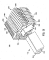
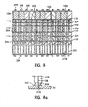
- Fig. 1 illustrates a two-part connector assembly 30 in accordance with the present invention including a socket connector 100 configured to be coupled to a daughtercard 32, and a header connector 400 configured to be coupled to a motherboard 34.
- Fig. 2 illustrates an exploded perspective view of the socket connector 100 in accordance with one aspect of the present invention.
- the socket connector 100 includes a front cap 102, seven horizontal shields 104 (sometimes referenced to herein as “third shields”), a plurality of connector modules 106 (also known as “wafers"), a plurality of vertical stripline shields 108 (sometimes referenced to herein as “first shields” or “first shield portions”), and eight laterally extending angled tailshields 110 (sometimes referenced to herein as “second shields” or “second shield portions”).
- first shields also known as “wafers”
- second shields eight laterally extending angled tailshields 110
- the front cap 102 includes a housing 120 made from insulating material, and having a generally vertically extending front wall 122 and a pair of laterally extending, horizontal top and bottom walls 124 and 126.
- the front wall 122 is formed to include a plurality pin-insertion windows 130 extending between an internal surface 132 and an external surface 134 thereof. As shown, the plurality of pin-insertion windows 130 are arranged in a grid form as an array of vertical columns and horizontal rows. In the illustrated embodiment, there are eight pin-insertion windows 130 in each column.
- the internal surface 132 of the front wall 122 is formed to include a plurality of inwardly extending, rectangular vertical dividers 140 having top surfaces 142 and bottom surfaces 144.
- the top surfaces 142 of rectangular dividers 140 and the bottom surfaces 144 of the adjacent higher rectangular dividers 140 cooperate to define seven laterally extending, horizontal slots 146 into which seven horizontal shields 104 are inserted to form eight horizontal compartments 148 in substantial alignment with eight rows of pin-insertion windows 130.
- Eight horizontal compartments 148 formed in the front cap 102 are configured to receive eight forwardly extending receptacle contacts 204 of the connector modules 106 and eight forwardly extending shield fingers 274 of the vertical stripline shields 108 when the connector modules 106 and the vertical stripline shields 108 are inserted into the front cap 102.
- the internal surface 132 of the front wall 122 is further formed to include a plurality of inwardly extending, preopening fingers 150, which are configured for insertion between opposed cantilevered beams 208 of the receptacle contacts 204 of the socket connector 100 to keep the cantilevered beams 208 separated. This facilitates insertion of signal pins 404 of the header connector 400 into the receptacle contacts 204 of the socket connector 100 when the two are mated as shown in Figs. 22 and 23 .
- the laterally extending top and bottom walls 124 and 126 each include internal surfaces 152 and external surfaces 154.
- the internal surfaces 152 of the top and bottom walls 124 and 126 are formed to include a plurality of inwardly extending guide slots 156 extending substantially perpendicularly therefrom for guiding insertion of a plurality of paired connector units 112, each comprising a vertical stripline shield 108 coupled to a connector module 106 along a first side 232 thereof as shown in Fig. 11 .
- the plurality of guide slots 156 are arranged in pairs - a narrower guide slot 158 for guiding insertion of a vertical stripline shield 108 and an adjacent broader guide slot 160 for guiding insertion of an associated connector module 106.
- the front cap 102 may be formed to include vertical end walls (not shown) extending between the laterally extending top and bottom walls 124 and 126 at the opposite ends thereof.
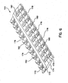
- Figs. 5 shows one of seven horizontal shields 104 (also referred to herein as "third shields") positioned to be inserted into one of seven laterally extending slots 146 formed in the front cap 102.
- Each horizontal shield 104 includes an inner layer of shielding material 170 sandwiched between outer layers of insulating material 172 and 174 as shown in Fig. 6 .
- the horizontal shields 104 may be formed as a continuous strip by using insert molding process.
- the front and back edges 176 of each horizontal shield 104 are formed to include a plurality of cut-outs 178 through which a plurality of flexible contacts 180 formed in the inner shielding layer 170 project.
- the flexible contacts 180 of the horizontal shields 104 are configured to electrically engage the forwardly extending shield fingers 274 of the vertical stripline shields 108 at the front and back ends of the forwardly extending shield fingers 274 upon insertion of the vertical stripline shields 108 into the front cap 102.
- the lateral spacing between the flexible contacts 180 of the horizontal shields 104 is the same as the lateral spacing between the forwardly extending shield fingers 274 of the vertical stripline shields when the vertical stripline shields 108 are inserted into the front cap 102.
- the horizontal shields 104 are formed to include guide slots 182 for guiding insertion of the vertical stripline shields 108 into the front cap 102 so that the forwardly extending shield fingers 274 of the vertical stripline shields 108 are aligned with the flexible contacts 180 of the horizontal shields 104.
- the outer insulating layers 172 and 174 of the horizontal shields 104 vertically separate and insulate the female receptacle contacts 204 of the connector modules 106 from each other.
- the inner shielding layers 170 of the horizontal shields 104 vertically shield the female receptacle contacts 204 of the connector modules 106 from each other.
- the horizontal and vertical shields 104 and 108 inserted into the front cap 102 cooperate to form a virtual coaxial shield around each female receptacle contact 204 of the connector modules 106.
- the use of two flexible contacts 180 at the front and back of the horizontal shields 104 serves to distribute ground currents radially around the receptacle contacts 204, thereby reducing crosstalk between neighbouring signals.
- Fig.7 shows the contact circuitry 200 encased in the overmolded connector module 106 made from insulating material.
- the contact circuitry 200 includes eight individual conductive current paths 202, each electrically connecting a single forwardly extending receptacle contact 204 to a corresponding downwardly extending pin tail 206.
- Each receptacle contact 204 includes a pair of opposed cantilevered beams 208 into which the signal pins 404 of the header connector 400 are inserted when the socket connector 100 and the header connector 400 are mated.
- Each conductive path 202 is formed to include a first leg portion 212 substantially parallel to an associated receptacle contact 204, a second leg portion 214 at an angle to the first leg portion 212, and a third leg portion 216 substantially parallel to an associated pin tail 206.
- the top and bottom conductive paths 202 are additionally formed to include retention flanges 218 near the upper and lower receptacle contacts 204.
- Fig.8 shows one of a plurality of connector modules 106 encasing eight individual conductive paths 202.
- the connector modules 106 may be also formed using insert moulding process.
- the connector module 106 is formed to include eight angled passageways 230 which are interleaved with the eight conductive paths 202, and which extend laterally between first and second sides 232 and 234 of the connector module.
- each laterally extending angled passageway 230 in the connector module 106 includes first and second leg portions 242 and 244 substantially parallel to the first and second leg portions 212 and 214 of an associated conductive path 202.
- the connector module 106 is formed to include a number of interlocking features for mating with corresponding interlocking features of the vertical stripline shield 108 to ensure good support and alignment therebetween, particularly during press fitting of the socket connector 100 onto a printed circuit board 32.
- the first side 232 of the connector module 106 is formed to include a horizontal recess 248 above the uppermost conductive path 202, a vertical recess 250 to the right of the uppermost conductive path 202, six small tabs 252 below the lowermost conductive path 202, and two large tabs 254 - one on each side of the six small tabs 252.
- the six small tabs 252 and the two large tabs 254 are each formed to have a raised area 262 around the outer periphery thereof to hold the vertical stripline shields 108 against the associated connector modules 106 to prevent the vertical stripline shields 108 from slipping during press fitting of the socket connector 100 onto a printed circuit board 32.
- the slipping of the vertical stripline shields 108 may cause the shield tails 276 to roll over or buckle.
- the second side 234 of each connector module 106 is formed to include a slot 264 extending along the bottom edge thereof into which the tabs 252 and 2 54 formed on the first side 232 of the adjacent connector module 106 are received.
- the downwardly facing surface 266 of the slot 266 overhangs over the tabs 252 and 254, and exerts a downward force on the upwardly facing surfaces of the tabs 252 and 254 during press fitting of the socket connector 100 onto a printed circuit board 32 to prevent the connector modules 106 from separating.
- the separation of the connector modules 106 may cause the pin tails 206 to roll over or buckle.
- the connector modules 106 are formed to include grip areas 269, which are used to line up the connector modules 106 prior to insertion of the laterally extending tailshields 110.
- the first sides 232 of the connector modules 106 are further formed to include three columns of support bumps 268 near the front, back and the middle of the connector modules 106 between the laterally extending angled passageways 230 therein.
- the support bumps 268 define the spacing between the connector modules 106 and the respective vertical stripline shields 108.
- the laterally extending angled tailshields 110 inserted in the laterally extending angled passageways 230 in the connector modules 106 cooperate with the three columns of support bumps 268 to lend rigidity to the socket structure.
- the support bumps 262 are configured to form air gaps around the conductive paths 202 in the connector modules 106 in an assembled socket connector 100.
- the geometry and dimensions of the air gaps surrounding the conductive paths 202 and the geometry and dimensions of the insulating and shielding materials surrounding the air gaps are configured to tune the socket connector 100 to match a specified impedance.
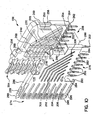
- Fig. 10 shows one of a plurality of vertical stripline shields 108 configured to be press fitted to an associated connector module 106 to form a paired connector unit 112.
- both the vertical stripline shields 108 and the connector modules 106 are formed to include a number of interlocking features that facilitate press fitting of the vertical stripline shield 108 to the connector module 106, and ensure good support and proper alignment of the corresponding elements when the two are press fitted.
- each vertical strip line shield 108 includes eight angled passageways 270 extending laterally between the opposite sides thereof in substantial alignment with the laterally extending angled passageways 230 in the connector modules 106, eight forwardly extending shield fingers 274 in substantial alignment with eight forwardly extending receptacle contacts 204 of the connector modules 106, eight downwardly extending shield tails 276 adjacent to eight downwardly extending pin tails 206 of the connector modules 106, a first horizontal cantilevered top flange 278 configured for reception in the horizontal recess 248 of the connector module 106, a first vertical cantilevered flange 280 configured for reception in the vertical recess 250 of the connector module 106, six small apertures 282 at the bottom for reception of six small tabs 252 of the connector module 106, two large slots 284 at the bottom for reception of two large tabs 254 of the connector module 106, a second horizontal cantilevered top flange 286 which fits over a top wall 256 of the connector module 106, a second horizontal can
- each laterally extending angled passageway 270 in the vertical stripline shield 108 includes first and second leg portions 292 and 294 substantially aligned with the first and second leg portions 242 and 244 of an associated, laterally extending angled passageway 230 in the connector module 106 to form laterally extending angled channels 304 in the paired connector units 112.
- Each vertical stripline shield 108 is further formed to include two pairs of opposed tabs 306 near the front and back of the vertical stripline shield 108.
- the opposed tabs 306 project into the laterally extending angled passageways 270 in the vertical stripfne shields 108, and are configured to electrically contact laterally extending angled tailshields 110 inserted in the laterally extending angled channels 304 in the paired connector units 112 to form a coaxial shield around each conductive path 202.
- the top and bottom horizontal cantilevered flanges 286 and 290 of the vertical stripline shield 108 slide over the external surfaces 154 of the top and bottom walls 124 and 126 of the front cap 102.
- the top and bottom horizontal cantilevered flanges 286 and 290 are formed to include top and bottom contact arms 296 to electrically engage corresponding top and bottom ground pins 408 of the header connector 400 as shown in Figs. 22 and 23 .
- the top and bottom horizontal cantilevered flanges 286 and 290 are additionally formed to include tabs 298 which are configured to slide into corresponding guide slots 128 in the top and bottom walls 124 and 126 of the front cap 102 to ensure alignment of the vertical stripline shields 208 with the front cap 102.
- each group of eight downwardly extending shield tails 276 is arranged as seven side shield tails 300 and one end shield tail 302 adjacent to a respective one of pin tails 206.
- the downwardly extending shield tails 276 of the vertical stripline shields 108 may be press fitted into the holes in a printed circuit board or soldered thereto.
- each vertical stripline shield 108 is designed to be press fitted onto a connector module 106 so that the eight laterally extending angled passageways 270 therein align with the eight laterally extending angled passageways 230 in the connector modules 106 to form eight laterally extending angled channels 304, the eight forwardly extending shield fingers 274 thereof align with the eight forwardly extending receptacle contacts 204 of the contact circuitry 200, the eight downwardly extending shield tails 276 therein are disposed adjacent to the eight downwardly extending pin tails 206 of the contact circuitry 200, the first horizontal cantilevered top flange 278 is inserted into the horizontal recess 248 of the connector module 106, the first vertical cantilevered flange 280 is inserted into the vertical recess 250 of the connector module 106, the six small tabs 252 of the connector module 106 are inserted into the six small apertures 282 in the vertical stripline shield 108, the two large tabs 254 of the connector module 106 are inserted into the two large slots 2
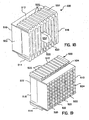
- Figs. 12 shows seven horizontal shields 104 inserted into seven laterally extending slots 146 in the front cap 102 to form eight laterally extending compartments 148 in substantial alignment with eight rows of pin-insertion windows 130 therein, and further shows one of a plurality of paired connector units 112 positioned for insertion into the front cap 102.
- the internal surfaces of the top and bottom walls 124 and 126 of the front cap 102 include a narrower guide slot 158 for guiding insertion of a vertical stripline shield 108 and a broader guide slot 160 for guiding insertion of an associated connector module 106.
- Figs. 12 shows seven horizontal shields 104 inserted into seven laterally extending slots 146 in the front cap 102 to form eight laterally extending compartments 148 in substantial alignment with eight rows of pin-insertion windows 130 therein, and further shows one of a plurality of paired connector units 112 positioned for insertion into the front cap 102.
- the laterally extending angled passageways 230 and 270 in the connector modules 106 and the vertical stripline shields 108 are aligned with each other to form a plurality of laterally extending angled channels 304 extending side-to-side between the opposite sides of the socket connector 100.
- the vertical dividers 140 in the front cap 102 horizontally separate the forwardly extending receptacle contacts 204 of the connector modules 106 from each other and from the forwardly extending shield fingers 274 of the associated vertical stripline shields 108.
- the horizontal shields 104 vertically separate the eight forwardly extending receptacle contacts 204 and the eight forwardly extending shield fingers 274 from each other:
- the flexible contacts 180 of the horizontal shields 104 electrically contact the forwardly extending shield fingers 274 of the vertical stripline shields 108 to form a coaxial shield around each receptacle contact 204.
- the use of two flexible contacts 180 at the front and back of the horizontal shields 104 serves to distribute the ground currents radially around the receptacle contacts 204, thereby reducing the crosstalk between neighbouring signals.
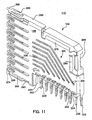
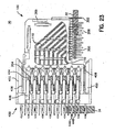
- Fig.13 shows eight laterally extending angled tailshields 110 positioned for insertion into the eight laterally extending angled channels 304 in the socket connector 100.
- Each laterally extending angled tailshield 110 is formed to include first and second leg portions 312 and 314 substantially aligned with the first and second leg portions 292 and 294 of the vertical stripline shields 108.
- the opposed tabs 306 of the eight vertical stripline shields 108 electrically contact the laterally extending angled tailshields 110 inserted into the eight laterally extending angled channels 304 to form a coaxial shield around each conductive path 202 as more clearly shown in Fig. 14 .
- the use of two pairs of opposed tabs 306 near the front and back of the vertical stripline shield 108 serves to distribute the ground currents radially around the conductive paths 202, thereby reducing the crosstalk between neighbouring signals.
- the laterally extending angled tailshields 1 10 may be formed instead by plating the laterally extending passageways 230 in the connector modules 106.
- Figs.15 , 15a and 16 show the header connector 400 in accordance with another aspect of the present invention.
- the header connector 400 includes a header body 402, a plurality of signal pins 404, a continuous strip having a plurality of shield blades 406 formed therein, and a plurality of around pins 408. Except for their length, the ground pins 408 are substantially identical to the signal pins 404.
- the header body 402 is formed to include a vertical front wall 410, and top and bottom laterally extending, horizontal walls 412 and 414 projecting perpendicularly therefrom.
- the front wall 410 is formed to include a plurality of first signal-pin-receiving openings 416, a plurality of second shield-blade-receiving openings 418, and a plurality of third ground-pin-receiving openings 420, all of which extend between the internal and external surfaces 422 and 424 thereof.
- the plurality of second shield-blade-receiving openings 418 are formed to have a generally right angle cross-section.
- the plurality of signal pins 404 are configured for insertion into the plurality of first signal-pin-receiving openings 416 in the header connector 400 to form an array of pin contacts 426 (shown in Fig.1 ) which are configured for reception in an array of pin-insertion windows 130 in the socket connector 100, when the socket connector 100 is inserted into the header connector 400.
- Each signal pin 404 includes a first end 452 extending above the front wall 410 of the header connector 400, and a second end 454 spaced apart from the first end 452 and configured for insertion into an opening 36 in a printed circuit board 34.
- the plurality of shield blades 406 are formed to include a generally right angle shielding portion 428 configured to be inserted into the plurality of second, generally right angle shield-blade-receiving openings 418.
- Each shield blade 406 includes a first end 462 extending above the front wall 410 of the header connector 400 adjacent to the first end 452 of a signal pin 404, and a second end 464 spaced apart from the first end 462 configured for insertion into a hole 38 in the printed circuit board 34 adjacent to the second end 454 of the signal pin 404.
- the generally right angle shielding portion 428 of each of the plurality of shield blades 406 includes substantially perpendicular first and second leg portions 430 and 432.
- first signal-pin-receiving openings 416 and the second shield-blade-receiving openings 418 are arranged symmetrically in the front wall 410 of the header body 402 such that the generally right angle shielding portions 428 of shield blades 406 substantially surround the signal pins 404 to form a coaxial shield around each of the plurality of signal pins 404.
- Each of the plurality of second, generally right angle shield-blade-receiving openings 418 includes a central portion 434 coupled to first and second end portions 436 and 438 by first and second narrowed throat portions 440 and 442.
- the first and second narrowed throat portions 440 and 442 are dimensioned to frictionally engage the first and second leg portions 430 and 432 of the shield blades 406 to hold the shield blades 406 in place.
- the central portion 434 and the first and second end portions 436 and 438 of each of the plurality of second generally right angle openings 418 are formed to provide air gaps 444 surrounding the generally right angle shielding portion 428 of a shield blade 406.
- the geometry and dimensions of the air gaps 444, the geometry, dimensions and material of the right angle shielding portions 428, and the geometry, dimensions and material of the header body 402 surrounding the air gaps 444 are configured to tune the header connector 400 to match a specified impedance (for example, 50 ohms).
- the configuration of the right angle shield blades 406 lends itself to mass production in a continuous strip in a manner that economises material usage.
- a plurality of ground pins 408 are configured for insertion into the plurality of third ground-pin-receiving openings 420 in the front wall 410 of the header connector 400.
- the plurality of ground pins 408 are configured to engage contact arms 296 of the corresponding vertical stripline shields 108 when the socket connector 400 is inserted into the header connector 100 as shown in Figs. 22 and 23 .
- Each ground pin 408 includes a first end 472 extending above the front wall 410 of the header connector 400, and a second end 474 spaced apart from the first end 472 and configured for insertion into a hole 40 in a printed circuit board 34.
- Each of a plurality of signal pins 404 includes a pin tail 446
- each of the plurality of shield blades 406 includes a shield tail 448.
- Fig. 17 is a perspective view showing first and second header bodies 402 positioned end to end, and one of a plurality of continuous strips of shield blades 406 configured for insertion into a row of shield-blade-receiving openings 418 in the first and second header bodies 402.
- the continuous strips of shield blades 406 extend between the first and second header bodies 402 to tie them together to form a monoblock.
- the continuous strips of shield blades 406 can be used to connect any number of header connectors 400 to create header connectors of variable length.
- the strip of shield blades 406 may be formed to include a right angle tab 406' at opposite ends thereof to provide a secure connection between the header bodies 402.
- Monoblocking can also be used on the socket side of the connectors.
- the horizontal tailshields 110 can extend between several adjoining socket housings 120 to couple them together.
- termination tools are typically made of steel, and include a bottom wall formed to include an array of holes for receiving the signal pins 404, shield blades 406 and ground pins 408 of the header connector 400 therein.
- the termination tools are used to install the header connector 400 onto a printed circuit board 34 at a customer's facility by pushing on the ends of the signal and ground pins 404 and 408 or on shoulders thereof.
- the holes in these termination tools may be formed at different depths to set the signal and ground pins 404 and 408 at different heights in the installed header connector 400. Illustratively, the difference in heights could be about 30/1,000 inch (8mm). Different height signal pins 404 are desirable for sequencing the circuits on the printed circuit board, for example, to power some circuits ahead of others.
- These conventional termination tools are typically precision-machined metal parts, and are relatively expensive.
- Figs.18-21 show a relatively inexpensive plastic protective cap 500 in accordance with still another aspect of the present invention, which doubles as a termination tool.
- the protective cap 500 protects the signal pins 404, the shield blades 406 and the ground pins 408 of the header connector 400 during shipping and handling of the header connector 400 until a socket connector 100 is plugged into the header connector 400 at a customer's facility, at which time the protective cap 500 may be removed from the header connector 400.
- the protective cap 500 is used to install the header connector 400 onto a printed circuit board 34 without the need for any additional application or termination tooling.
- the protective cap 500 includes a body 502 having a front wall 510, a top wall 512, a bottom wall 514 and back wall 516.
- the cap body 502 is formed to include a plurality of ribs 520 that extend between the front and back walls 5 110 and 516 thereof to define a plurality of through slots 522 therein.
- the slots 522 are configured to receive the planar first ends 462 of the shield blades 406 when the protective cap 500 is inserted into the header body 400.
- the ribs 520 ate. in turn, formed to include a plurality of holes 524 therein configured to receive the first ends 452 and 472 of the signal pins 404 and the ground pins 408.
- the external surfaces of the top and bottom walls 512 and 514 are formed to include a plurality of guide grooves 550 which are configured to engage corresponding plurality of guide portions 450 formed on the internal surfaces of the top and bottom walls 412 and 414 of the header connector 400 when the protective cap 500 is inserted into the header connector 400.
- the engagement between the guide grooves 550 in the protective cap 500 and the guide portions 450 in the header connector 400 serve to align the shield-blade-receiving slots 522 in the protective cap 500 with the shield blades 406 in the header connector 400, and the signal and ground pin-receiving holes 524 in the protective cap 500 with the signal and ground pins 404 and 408 in the header connector 400.
- the header connector 400 is shipped to a customer's facility with a protective cap 500 in place.
- the protective cap 500 protects the signal pins 404, the shield blades 406 and the ground pins 408 during shipping and handling of the protective cap 500 to a customer's facility.
- the protective cap 500 doubles as an application or termination tool to press fit the header connector 400 onto a printed circuit board 34.
- the holes 524 moulded in the ribs 530 in the protective cap 500 may be formed to vary in depths to allow the signal pins 404 and the ground pins 408 to float up during press fitting the header connector 400 onto a printed circuit board 34.
- the force generated by press fitting the header connector 400 onto a printed circuit board 34 is larger than the force required to move the signal pins 404 and the ground pins 408 in the header body 402.
- the signal pins 404 and the ground pins 408 in the header body 402 move up in the header body 402 until the ends 452 and 472 of the signal pins 404 and the ground pins 408 engage the end surfaces 526 of the holes 524 in the protective cap 500.
- the end surfaces 526 of the holes 524 in the protective cap 500 push on the ends 452 and 472 of the signal and ground pins 404 and 408 during press fitting of the header connector 400 onto a printed circuit board 34.
- the back wall 516 of the protective cap is formed to include a tab 552 that is used for removing the protective cap 500 from the header connector 400 prior to insertion of a socket connector 100 therein.
- the protective cap 500 is moulded from relatively inexpensive thermoplastic material.
- the thermoplastic material is soft enough so that the ends 452 and 472 of the signal and ground pins 404 and 408 will not be damaged during installation of the header connector 400 onto a printed circuit board 34.
- the thermoplastic material is not too soft to allow the ends 452 and 472 to puncture the walls of the protective cap 500 more than a few thousands of an inch (2 mm).
- Figs.23 and 24 show assembly of the socket connector 100 with the header connector 400.
- External guide means such as card guides or guide pins (not shown) are provided on the opposite sides of the header connector 400 to guide the insertion of the socket connector 100 into the header connector 400 - so that the array of pin-insertion windows 130 in the socket connector 100 are aligned with the array of pin contacts 426 in the header connector 400 prior to insertion of the pin contacts 426 into the receptacle contacts 204 of the socket connector 100.
- the shield blades 406 of the header connector 400 contact corresponding shield fingers 274 of the socket connector 100
- the ground pins 408 of the header connector 400 contact corresponding contact arms 296 of the vertical stripline shields 106.
- the pin tails 206 and shield tails 276 of the socket connector 100 and the pin tails 446 and shield tails 448 of the header connector 400 can be either press fitted into the holes in the printed circuit boards or soldered thereto.
- the pin tails 206 and 446 and shield tails 276 and 448 could instead be surface mounted to the printed circuit boards.
- the vertical stripline shields 108 (sometimes referred to herein as “first shields” or “first shield portions”) cooperate with the laterally extending tailshields 110 (sometimes referred to herein as “second shields” or “second shield portions”) inserted into the laterally extending angled channels 304 in the socket connector 100 to form a coaxial shield around each conductive path 202.
- the vertical stripline shields 108 further cooperate with the horizontal shields 104 (sometimes referred to herein as "third shields”) to form a coaxial shield around each receptacle contact 204 of the socket connector 100.
- the generally right angle shield blades 406 of the header connector 400 substantially surround the signal pins 404 of the header connector 400 to form a coaxial shield around each of the plurality of signal pins 404.
- the connector materials, geometry and dimensions are all designed to maintain a specified impedance throughout the part.
- the socket connector 100 of the present invention can be reconfigured to form differential pairs in columns and rows. For example, every other vertical stripline shield 108 can be removed in the socket connector 100 to form differential pairs in rows. Likewise, every other horizontal shield 104 and every other tailshield 110 can be removed in the socket connector 100 to form differential pairs in columns.
- connector assembly 30 is designed to make connections which are a multiple of eight (8), it will be noted that the connector assembly 30 in accordance with the present invention may very well be designed to make connections which are a multiple of a number other than eight (8).
- the design of the illustrated connector assembly 30 lends itself to the creation of connectors which are of a variable length.
- the continuous strips of shield blades 406 can be used to connect any number of header connectors 400 to create header connectors of variable length.
- Monoblocking can also be used on the socket side of the connectors.
- the horizontal tailshields 110 can extend between several adjoining socket housings 120 to couple them together.
- thermoplastic material such as liquid crystal polymer (''LCP").
- the protective cap 500 may be moulded from nylon.
- the metallic parts are made from plated copper alloy material.
Abstract
Description
- This invention relates to two-part electrical connectors, and particularly to two-part high-speed backplane electrical connectors. More particularly, this invention relates to improvements in shielded two-part high-speed backplane electrical connectors.
- Conductors carrying high frequency signals and currents are subject to interference and cross talk when placed in close proximity to other conductors carrying high frequency signals and currents. This interference and cross talk can result in signal degradation and errors in signal reception. Coaxial and shielded cables are available to carry signals from a transmission point to a reception point, and reduce the likelihood that the signal carried in one shielded or coaxial cable will interfere with the signal carried by another shielded or coaxial cable in close proximity. However, at points of connection, the shielding is often lost allowing interference and crosstalk between signals. The use of individual shielded wires and cables is not desirable at points of connections due to the need for making a large number of connections in a very small space. In these circumstances, two-part high-speed backplane electrical connectors containing multiple shielded conductive paths are used.
- This design is based on, but not limited to, the industry standard for a two-part high-speed backplane electrical connector for electrically coupling a motherboard (also known as "backplane") to a daughtercard is set forth in the United States by specification IEC 1076-4-101 from the International Electrotechnical Commission. This specification sets out parameters for 2mm, two-part connectors for use with printed circuit boards. The IEC specification defines a socket connector that includes female receptacle contacts and a header connector that contains male pin contacts configured for insertion into the female receptacle contacts of the socket connector.
- In accordance with the present invention, a two-part high-speed backplane electrical connector with improved electromagnetic shielding is disclosed. The two-part connector comprises a socket connector and a header connector.
- According to a first embodiment of the current invention, the socket connector includes an electrical connector comprising:
- a housing,
- a plurality of horizontal shields configured for insertion into the housing, and
- a plurality of connector modules configured for insertion into the housing, each connector module including an insulated material encasing a plurality of conductive paths, each coupled to a forwardly-extending receptacle contact, the receptacle contacts are formed to include a plurality of horizontally-extending slots configured to receive the horizontal shields when the connector modules are inserted into the housing.
- In accordance with another aspect of the first embodiment of the invention, a socket connector includes an electrical connector comprising:
- a plurality of connector modules, each connector module including an insulated material encasing a plurality of conductive paths, each connector module being further formed to include a plurality of laterally-extending openings which are interleaved with the plurality of conductive paths, a plurality of shields including first shield portions extending along first sides of the plurality of connector modules and second shield portions extending into the laterally-extending openings in the plurality of connector modules to form coaxial shields around the conductive paths, and a housing configured to receive the plurality of connector modules and shields.
- According to yet another aspect of the first embodiment of the invention, a socket connection includes an electrical connector comprising:
- a housing,
- a plurality of connector modules configured for insertion into the housing, each connector module including an insulated material encasing a plurality of conductive paths, each connector module being further formed to include a plurality of passageways which are interleaved with the plurality of conductive paths, and which extend laterally between opposite sides of the connector modules,
- a plurality of first shields configured for insertion into the housing, each first shield extending along a first side of an associated connector module, the first shields being formed to include a plurality of passageways extending laterally between opposite sides thereof in substantial alignment with the passageways in the connector modules to form a plurality of laterally-extending channels, and
- a plurality of second shields configured for insertion into the plurality of laterally-extending channels in the plurality of connector modules and first shields, the second shields being electrically coupled to the first shields to form coaxial shields around the conductive paths.
- According to still another aspect of the first embodiment of the invention, an electrical connector includes an electrical connector comprising:
- a housing,
- a plurality of connector modules, each connector module including an insulated material encasing a plurality of conductive paths, the plurality of connector modules being coupled to the housing, each connector module being formed to include a plurality of passageways which are interleaved with the plurality of conductive paths,
- a plurality of first shields extending along a first side of an associated connector module, and
- a plurality of second shields, each second shield being configured for insertion into one of the passageways formed by the plurality of connector modules, the plurality of first shields being electrically coupled to the plurality of second shields to form coaxial shields around the conductive paths.
- In accordance with a second embodiment of the current invention, a socket connector includes an electrical connector comprising:
- a body formed to include a front wall, a back wall, and a plurality of first and second openings extending through the body to provide a passageway through the front and back walls,
- a plurality of signal pins configured for insertion into the plurality of first openings, each signal pin including a first end extending from the front wall of the body to form an array of pin contacts, and a second end spaced apart from the first end and extending from the back wall of the body, and
- a plurality of shield blades configured for insertion into the plurality of second openings, each of the plurality of shield blades having a first end extending from the front wall of the body adjacent to the first end of a signal pin, a second end extending from the back wall of the body adjacent to the second end of said signal pin and a generally right angle shielding portion configured to be disposed adjacent to an intermediate portion of said signal pin.
- According to a further aspect of the second embodiment, an electrical connector includes an electrical connector comprising:
- a body formed to include a front wall, a back wall, and a plurality of first and second openings extending through the body to provide a passageway through the front and back walls,
- a plurality of signal pins configured for insertion into the plurality of first openings, each signal pin including a first end extending from the front wall of the body to form an array of pin contacts, and a second end spaced apart from the first end and extending from the back wall of the body, and
- a plurality of shield blades configured for insertion into the plurality of second openings, each of the plurality of shield blades having a first end extending from the front wall of the body adjacent to the first end of a signal pin, a second end extending from the back wall of the body adjacent to the second end of said signal pin and a generally right angle shielding portion configured to be disposed adjacent to an intermediate portion of said signal pin, wherein the first and second openings are arranged in the body such that the generally right angle shielding portions of shield blades substantially surround the signal pins.
- The detailed description particularly refers to the accompanying figures in which:
-
Fig. 1 is a perspective view of a connector assembly in accordance with the present invention showing a socket connector having an array of female receptacle contacts positioned for insertion into a header connector having a corresponding array of male pin contacts, -
Fig. 2 is an exploded view of the socket connector ofFig. 1 in accordance with one aspect of the present invention, and showing, from left to right, a front cap including a front wall having an inner surface formed to include a plurality of vertically extending rectangular dividers, one of seven horizontal shields (sometimes referred to herein as "third shields") configured for insertion into one of seven laterally extending slots in the vertically extending rectangular dividers to form eight laterally extending compartments, one of a plurality of connector modules having eight forwardly extending female receptacle contacts internally coupled to eight downwardly extending pin tails, one of a plurality of vertical stripline shields (sometimes referred to herein as "first shields") having eight forwardly extending shield fingers and eight downwardly extending shield tails configured to be to extend along a first side of the connector module so that eight forwardly extending shield fingers of the vertical stripline shield are generally aligned with eight forwardly extending receptacle contacts of the connector module and eight downwardly extending shield tails of the vertical stripline shield are disposed adjacent to the eight downwardly extending pin tails of the connector module, both the connector modules and the stripline shields having eight laterally extending angled passageways therethrough into which eight laterally extending angled tailshields (sometimes referred to herein as "second shields") are inserted to form a coaxial shield around each conductive path in the connector modules, -
Fig.3 is a perspective view of the front cap ofFig. 2 rotated anticlockwise approximately 60 degrees from the orientation shown inFig. 2 , and showing an array of pin-insertion windows formed in the front wall, the array of pin insertion windows being arranged in columns of eight pin-insertion windows, -
Fig. 4 is a perspective view of the front cap ofFigs. 2-3 shown in the same orientation as shown inFig. 2 , and more fully showing vertically extending rectangular dividers projecting inwardly from the front wall for horizontally separating the receptacle contacts of the connector modules and for vertically separating the horizontal shields, and further showing a plurality of preopening fingers projecting inwardly from the front wall and arranged for insertion into opposed cantilevered fingers of the receptacle contacts for facilitating insertion of pin contacts of the header connector therein, and a plurality of guide slots formed in the internal surfaces of the top and bottom laterally extending walls of the front cap for guiding insertion of the connector modules and vertical stripline shields therein, -
Fig. 5 is a perspective view of one of seven horizontal shields configured to be inserted into one of seven laterally extending slots between the inwardly extending rectangular dividers in the front cap, seven horizontal shields forming eight laterally. extending compartments in the front cap for vertically separating and shielding eight receptacle contacts of the connector modules from each other, -
Fig. 6 is an enlarged perspective view of the horizontal shield including an inner layer of shielding material sandwiched between two outer layers of insulating material, the front and back edges of the horizontal shields being formed to include a plurality of cut-outs through which a plurality of flexible contacts of the inner shielding layer project for electrically contacting the forwardly extending shield fingers of the vertical stripline shields near the front and back of the horizontal shields when the connector modules and vertical stripline shields are inserted into the front cap to form a coaxial shield around each receptacle contact, -
Fig. 7 is a perspective view of contact circuitry encased in the connector module, and showing eight separate conductive paths. each electrically connecting a single forwardly extending receptacle contact to the left of figure to a corresponding downwardly extending pin tail to the bottom-right of figure, -
Fig. 8 is a perspective view of one of a plurality of connector modules showing an insulated case encasing eight individual conductive paths, eight forwardly extending receptacle contacts each having two opposed cantilevered fingers to the left of figure, eight downwardly extending pin tails to the bottom-right of figure, eight laterally extending angled passageways therethrough which are interleaved with eight conductive paths therein for receiving eight laterally extending angled tailshields, a horizontal recess above the uppermost conductive path into which a horizontal cantilevered flange of an associated vertical stripline shield is inserted, a vertical recess to the right of the uppermost conductive path into which a vertical cantilevered flange of the associated vertical stripline shield is inserted, and further showing a number of interlocking features designed to facilitate press fitting of the vertical stripline shield to the connector module, -
Fig. 9 is an enlarged perspective view showing interlocking of adjacent connector modules; each connector module being formed to include a plurality of tabs on a first side thereof which are received in a cut-out formed on the second side of an adjacent connector module to prevent the connector modules from separating when the socket connector is press fitted onto a printed circuit board, -
Fig. 10 is a perspective view of one of a plurality of vertical stripline shields configured to be coupled to an associated connector module to form a paired connector unit, each vertical stripline shield including eight forwardly extending shield fingers to the left of figure each aligned with a forwardly extending receptacle contact of an associated connector module, eight downwardly extending shield tails to the bottom right of figure which are disposed adjacent to the downwardly extending pin tails of the connector module, eight laterally extending angled passageways configured to be aligned with eight laterally extending angled passageways in the connector module, six small apertures at the bottom for receiving six small tabs of the connector module, two large slots for receiving two large tabs of the connector module, a horizontal cantilevered flange for extending into the horizontal recess in the connector module, and a vertical cantilevered flange for extending into the vertical recess in the connector module, -
Fig.11 is a perspective view of a paired connector unit showing a vertical stripline shield press fitted to an associated connector module so that eight forwardly extending shield fingers of the vertical stripline shield are aligned with eight forwardly extending receptacle contacts of the connector module, eight downwardly extending shield tails of the vertical stripline shield are disposed adjacent to eight downwardly extending pin tails of the connector module, eight laterally extending angled passageways in the vertical stripline shield are aligned with eight laterally extending angled passageways in the connector module, six small tabs of the connector module are received in six small apertures in the vertical stripline shield, two large tabs of the connector module are received in two large slots in the vertical stripline shield, a horizontal cantilevered flange of the vertical stripline shield is inserted into the horizontal recess in the connector module, and a vertical cantilevered flange of the vertical stripline shield is inserted into the vertical recess in the connector module, -
Fig.12 is a perspective view showing a front cap having seven horizontal shields inserted into the seven laterally extending slots between the inwardly extending rectangular vertical dividers in the front wall to form eight horizontally extending compartments in substantial alignment with eight rows of pin-insertion windows, and further showing a paired connector unit aligned with a pair of guide slots formed in the top and bottom walls of the front cap, the vertical dividers horizontally separating the forwardly extending receptacle contacts of the connector modules from each other and from the forwardly extending shield fingers of the vertical stripline shields, the horizontal shields vertically separating the eight forwardly extending receptacle contacts and the eight forwardly extending shield fingers from each other, the flexible contacts at the front and back of the horizontal shields contacting the forwardly extending shield fingers of the vertical stripline shield to form a coaxial shield around each receptacle contact, -
Fig. 13 is a perspective view showing a partially assembled socket connector to the right of figure, and further showing eight laterally extending angled tailshields to the left of figure positioned for insertion into eight laterally extending angled channels in the connector modules and vertical strip line shields, the vertical stripline shields having two pairs of opposed tabs projecting into the laterally extending angled passageways therein for electrically contacting the laterally extending tailshields to form a coaxial shield around each conductive path, -
Fig. 14 is a cross-sectional view showing horizontal tailshields inserted into the laterally extending angled channels across the connector modules and the 5 vertical stripline shields to form a coaxial shield around each conductive path, -
Fig.14a is a cross-sectional view showing surface mounting of the pin tails of the socket connector to a printed circuit board, alternatively - the pin tails may be press fitted into the holes in the printed circuit board or soldered thereto,Fig. 15 is an exploded perspective view of the header connector ofFig. 1 according to another aspect of the present invention, and showing a signal pin, a continuous strip of shield blades, a ground pin and a header body, the header body including a front wall, top and bottom laterally extending walls extending perpendicularly from the front wall, and a plurality of first, second and third openings in the front wall for receiving a plurality of signal pins, shield blades and ground pins therein, -
Fig. 15 a is a perspective view of the continuous strip ofshield blades 406 ofFig. 15 , -
Fig. 16 is a cross-sectional view of the front wall of the header connector showing signal pins surrounded by right angle portions of the shield blades forming coaxial shields around each signal pin, -
Fig. 17 is a perspective view showing two header bodies positioned end 1 to end, and a strip of shield blades extending across the two header bodies, the strip of the header blades being configured to be inserted into the two header bodies to connect them together to form a monoblock, -
Fig. 18 is a perspective view of a protective cap in accordance with still another aspect of the present invention, the protective cap protecting the signal pins, the shield blades and the ground pins of the header connector during shipping and handling of the header connector to a customer's facility and also serving to aid the installation of the header connector onto a printed circuit board at the customer's facility, -
Fig.19 is a perspective view of the protective cap ofFig. 17 , turned 180 degrees from the position shown inFig. 17 to show a plurality of ribs formed in the front wall thereof, a plurality of slots for receiving the shield blades of the header connector and a plurality of holes formed in the ribs for receiving the signal pins and the ground pins of the header connector, -
Fig.20 is a perspective view showing the protective cap ofFigs. 18 and 19 inserted into the header connector, the protective cap being partially broken away on one side to show the signal pins and the shield blades of the header connector, -
Fig.21 shows a cross-sectional view of the protective cap of Figs. 1820 showing signal pins, shield blades and ground pins of the header connector inserted into the holes and slots in the protective cap, -
Fig.22 shows a socket connector partially inserted into a header connector so that the array of pin-insertion windows in the socket connector are aligned with the array of pin contacts in the header connector prior to the reception of the pin contacts in the header connector in the receptacle contacts in the socket connector, and -
Fig.23 shows the socket connector fully inserted into the header connector so that the pin contacts of the header connector are received in the receptacle contacts of the socket connector, shield blades of the header connector are in engagement with the shield fingers of the socket connector, and the ground pins of the header connector are in engagement with the contact arms of the socket connector. - While the connector assembly in accordance with the present invention may be designed to facilitate making any number of simultaneous electrical connections, the illustrated connector assembly is designed to facilitate making electrical connections which are a multiple of eight (8). Specifically, it will be understood that the connector assembly in accordance with the present invention may be designed to facilitate making electrical connections which are a multiple of any other number, such as two (2).
- Referring now to the drawings,
Fig. 1 illustrates a two-part connector assembly 30 in accordance with the present invention including asocket connector 100 configured to be coupled to adaughtercard 32, and aheader connector 400 configured to be coupled to amotherboard 34.Fig. 2 illustrates an exploded perspective view of thesocket connector 100 in accordance with one aspect of the present invention. Thesocket connector 100 includes afront cap 102, seven horizontal shields 104 (sometimes referenced to herein as "third shields"), a plurality of connector modules 106 (also known as "wafers"), a plurality of vertical stripline shields 108 (sometimes referenced to herein as "first shields" or "first shield portions"), and eight laterally extending angled tailshields 110 (sometimes referenced to herein as "second shields" or "second shield portions"). For the sake of clarity, only one each of the sevenhorizontal shields 104, the plurality ofconnector modules 106 and the plurality of vertical stripline shields 108 are shown inFig. 2 . - As shown more clearly in
Figs. 3 and4 , thefront cap 102 includes ahousing 120 made from insulating material, and having a generally vertically extendingfront wall 122 and a pair of laterally extending, horizontal top andbottom walls front wall 122 is formed to include a plurality pin-insertion windows 130 extending between aninternal surface 132 and anexternal surface 134 thereof. As shown, the plurality of pin-insertion windows 130 are arranged in a grid form as an array of vertical columns and horizontal rows. In the illustrated embodiment, there are eight pin-insertion windows 130 in each column. Theinternal surface 132 of thefront wall 122 is formed to include a plurality of inwardly extending, rectangularvertical dividers 140 havingtop surfaces 142 and bottom surfaces 144. The top surfaces 142 ofrectangular dividers 140 and the bottom surfaces 144 of the adjacent higherrectangular dividers 140 cooperate to define seven laterally extending,horizontal slots 146 into which sevenhorizontal shields 104 are inserted to form eighthorizontal compartments 148 in substantial alignment with eight rows of pin-insertion windows 130. Eighthorizontal compartments 148 formed in thefront cap 102 are configured to receive eight forwardly extendingreceptacle contacts 204 of theconnector modules 106 and eight forwardly extendingshield fingers 274 of the vertical stripline shields 108 when theconnector modules 106 and the vertical stripline shields 108 are inserted into thefront cap 102. - The
internal surface 132 of thefront wall 122 is further formed to include a plurality of inwardly extending,preopening fingers 150, which are configured for insertion between opposedcantilevered beams 208 of thereceptacle contacts 204 of thesocket connector 100 to keep thecantilevered beams 208 separated. This facilitates insertion of signal pins 404 of theheader connector 400 into thereceptacle contacts 204 of thesocket connector 100 when the two are mated as shown inFigs. 22 and23 . - The laterally extending top and
bottom walls internal surfaces 152 andexternal surfaces 154. Theinternal surfaces 152 of the top andbottom walls guide slots 156 extending substantially perpendicularly therefrom for guiding insertion of a plurality of pairedconnector units 112, each comprising avertical stripline shield 108 coupled to aconnector module 106 along afirst side 232 thereof as shown inFig. 11 . The plurality ofguide slots 156 are arranged in pairs - anarrower guide slot 158 for guiding insertion of avertical stripline shield 108 and an adjacentbroader guide slot 160 for guiding insertion of an associatedconnector module 106. Thefront cap 102 may be formed to include vertical end walls (not shown) extending between the laterally extending top andbottom walls -
Figs. 5 shows one of seven horizontal shields 104 (also referred to herein as "third shields") positioned to be inserted into one of seven laterally extendingslots 146 formed in thefront cap 102. Eachhorizontal shield 104 includes an inner layer of shieldingmaterial 170 sandwiched between outer layers of insulatingmaterial Fig. 6 . Thehorizontal shields 104 may be formed as a continuous strip by using insert molding process. The front andback edges 176 of eachhorizontal shield 104 are formed to include a plurality of cut-outs 178 through which a plurality offlexible contacts 180 formed in theinner shielding layer 170 project. Theflexible contacts 180 of thehorizontal shields 104 are configured to electrically engage the forwardly extendingshield fingers 274 of the vertical stripline shields 108 at the front and back ends of the forwardly extendingshield fingers 274 upon insertion of the vertical stripline shields 108 into thefront cap 102. The lateral spacing between theflexible contacts 180 of thehorizontal shields 104 is the same as the lateral spacing between the forwardly extendingshield fingers 274 of the vertical stripline shields when the vertical stripline shields 108 are inserted into thefront cap 102. Thehorizontal shields 104 are formed to includeguide slots 182 for guiding insertion of the vertical stripline shields 108 into thefront cap 102 so that the forwardly extendingshield fingers 274 of the vertical stripline shields 108 are aligned with theflexible contacts 180 of the horizontal shields 104. The outer insulatinglayers horizontal shields 104 vertically separate and insulate thefemale receptacle contacts 204 of theconnector modules 106 from each other. On the other hand, the inner shielding layers 170 of thehorizontal shields 104 vertically shield thefemale receptacle contacts 204 of theconnector modules 106 from each other. Thus the horizontal andvertical shields front cap 102 cooperate to form a virtual coaxial shield around eachfemale receptacle contact 204 of theconnector modules 106. The use of twoflexible contacts 180 at the front and back of thehorizontal shields 104 serves to distribute ground currents radially around thereceptacle contacts 204, thereby reducing crosstalk between neighbouring signals. -
Fig.7 shows thecontact circuitry 200 encased in theovermolded connector module 106 made from insulating material. Thecontact circuitry 200 includes eight individual conductivecurrent paths 202, each electrically connecting a single forwardly extendingreceptacle contact 204 to a corresponding downwardly extendingpin tail 206. Eachreceptacle contact 204 includes a pair of opposedcantilevered beams 208 into which the signal pins 404 of theheader connector 400 are inserted when thesocket connector 100 and theheader connector 400 are mated. Eachconductive path 202 is formed to include afirst leg portion 212 substantially parallel to an associatedreceptacle contact 204, asecond leg portion 214 at an angle to thefirst leg portion 212, and athird leg portion 216 substantially parallel to an associatedpin tail 206. The top and bottomconductive paths 202 are additionally formed to includeretention flanges 218 near the upper andlower receptacle contacts 204. -
Fig.8 shows one of a plurality ofconnector modules 106 encasing eight individualconductive paths 202. Theconnector modules 106 may be also formed using insert moulding process. Theconnector module 106 is formed to include eightangled passageways 230 which are interleaved with the eightconductive paths 202, and which extend laterally between first andsecond sides angled passageway 230 in theconnector module 106 includes first andsecond leg portions second leg portions conductive path 202. Theconnector module 106 is formed to include a number of interlocking features for mating with corresponding interlocking features of thevertical stripline shield 108 to ensure good support and alignment therebetween, particularly during press fitting of thesocket connector 100 onto a printedcircuit board 32. For example, thefirst side 232 of theconnector module 106 is formed to include ahorizontal recess 248 above the uppermostconductive path 202, avertical recess 250 to the right of the uppermostconductive path 202, sixsmall tabs 252 below the lowermostconductive path 202, and two large tabs 254 - one on each side of the sixsmall tabs 252. - The six
small tabs 252 and the twolarge tabs 254 are each formed to have a raisedarea 262 around the outer periphery thereof to hold the vertical stripline shields 108 against the associatedconnector modules 106 to prevent the vertical stripline shields 108 from slipping during press fitting of thesocket connector 100 onto a printedcircuit board 32. The slipping of the vertical stripline shields 108 may cause theshield tails 276 to roll over or buckle. Likewise, as shown inFig. 9 , thesecond side 234 of eachconnector module 106 is formed to include aslot 264 extending along the bottom edge thereof into which thetabs 252 and 2 54 formed on thefirst side 232 of theadjacent connector module 106 are received. The downwardly facingsurface 266 of theslot 266 overhangs over thetabs tabs socket connector 100 onto a printedcircuit board 32 to prevent theconnector modules 106 from separating. The separation of theconnector modules 106 may cause thepin tails 206 to roll over or buckle. Theconnector modules 106 are formed to includegrip areas 269, which are used to line up theconnector modules 106 prior to insertion of the laterally extending tailshields 110. - Again referring to
Fig. 8 , thefirst sides 232 of theconnector modules 106 are further formed to include three columns of support bumps 268 near the front, back and the middle of theconnector modules 106 between the laterally extendingangled passageways 230 therein. The support bumps 268 define the spacing between theconnector modules 106 and the respective vertical stripline shields 108. The laterally extendingangled tailshields 110 inserted in the laterally extendingangled passageways 230 in theconnector modules 106 cooperate with the three columns of support bumps 268 to lend rigidity to the socket structure. The support bumps 262 are configured to form air gaps around theconductive paths 202 in theconnector modules 106 in an assembledsocket connector 100. The geometry and dimensions of the air gaps surrounding theconductive paths 202 and the geometry and dimensions of the insulating and shielding materials surrounding the air gaps are configured to tune thesocket connector 100 to match a specified impedance. -
Fig. 10 shows one of a plurality of vertical stripline shields 108 configured to be press fitted to an associatedconnector module 106 to form a pairedconnector unit 112. As previously indicated, both the vertical stripline shields 108 and theconnector modules 106 are formed to include a number of interlocking features that facilitate press fitting of thevertical stripline shield 108 to theconnector module 106, and ensure good support and proper alignment of the corresponding elements when the two are press fitted. For example, each verticalstrip line shield 108 includes eightangled passageways 270 extending laterally between the opposite sides thereof in substantial alignment with the laterally extendingangled passageways 230 in theconnector modules 106, eight forwardly extendingshield fingers 274 in substantial alignment with eight forwardly extendingreceptacle contacts 204 of theconnector modules 106, eight downwardly extendingshield tails 276 adjacent to eight downwardly extendingpin tails 206 of theconnector modules 106, a first horizontal cantileveredtop flange 278 configured for reception in thehorizontal recess 248 of theconnector module 106, a first vertical cantileveredflange 280 configured for reception in thevertical recess 250 of theconnector module 106, sixsmall apertures 282 at the bottom for reception of sixsmall tabs 252 of theconnector module 106, twolarge slots 284 at the bottom for reception of twolarge tabs 254 of theconnector module 106, a second horizontal cantileveredtop flange 286 which fits over atop wall 256 of theconnector module 106, a second vertical cantileveredflange 288 which fits over aback wall 258 of theconnector module 106, and a third horizontal cantileveredbottom flange 290 which fits over abottom wall 260 of theconnector module 106. - As shown in
Fig. 10 , each laterally extendingangled passageway 270 in thevertical stripline shield 108 includes first andsecond leg portions second leg portions angled passageway 230 in theconnector module 106 to form laterally extendingangled channels 304 in the pairedconnector units 112. Eachvertical stripline shield 108 is further formed to include two pairs ofopposed tabs 306 near the front and back of thevertical stripline shield 108. Theopposed tabs 306 project into the laterally extendingangled passageways 270 in the vertical stripfne shields 108, and are configured to electrically contact laterally extendingangled tailshields 110 inserted in the laterally extendingangled channels 304 in the pairedconnector units 112 to form a coaxial shield around eachconductive path 202. - The top and bottom horizontal
cantilevered flanges vertical stripline shield 108 slide over theexternal surfaces 154 of the top andbottom walls front cap 102. The top and bottom horizontalcantilevered flanges bottom contact arms 296 to electrically engage corresponding top and bottom ground pins 408 of theheader connector 400 as shown inFigs. 22 and23 . The top and bottom horizontalcantilevered flanges tabs 298 which are configured to slide intocorresponding guide slots 128 in the top andbottom walls front cap 102 to ensure alignment of the vertical stripline shields 208 with thefront cap 102. It will be understood that the top andbottom contact arms 296 and the top andbottom tabs 298 of the vertical stripline shields 108 are optional and may be eliminated. As shown inFig. 11 , each group of eight downwardly extendingshield tails 276 is arranged as sevenside shield tails 300 and oneend shield tail 302 adjacent to a respective one ofpin tails 206. The downwardly extendingshield tails 276 of the vertical stripline shields 108 may be press fitted into the holes in a printed circuit board or soldered thereto. - Thus each vertical stripline shield 108 is designed to be press fitted onto a connector module 106 so that the eight laterally extending angled passageways 270 therein align with the eight laterally extending angled passageways 230 in the connector modules 106 to form eight laterally extending angled channels 304, the eight forwardly extending shield fingers 274 thereof align with the eight forwardly extending receptacle contacts 204 of the contact circuitry 200, the eight downwardly extending shield tails 276 therein are disposed adjacent to the eight downwardly extending pin tails 206 of the contact circuitry 200, the first horizontal cantilevered top flange 278 is inserted into the horizontal recess 248 of the connector module 106, the first vertical cantilevered flange 280 is inserted into the vertical recess 250 of the connector module 106, the six small tabs 252 of the connector module 106 are inserted into the six small apertures 282 in the vertical stripline shield 108, the two large tabs 254 of the connector module 106 are inserted into the two large slots 284 in the vertical stripline shield 108, the second horizontal cantilevered top flange 286 of the vertical stripline shield 108 fits over the top wall 256 of the connector module 106, the second vertical cantilevered flange 288 of the vertical stripline shield 108 fits over the back wall 258 of the connector module 106, and the third horizontal cantilevered bottom flange 290 fits over the bottom wall 260 of the connector module 106.
-
Figs. 12 shows sevenhorizontal shields 104 inserted into seven laterally extendingslots 146 in thefront cap 102 to form eight laterally extendingcompartments 148 in substantial alignment with eight rows of pin-insertion windows 130 therein, and further shows one of a plurality of pairedconnector units 112 positioned for insertion into thefront cap 102. As shown therein, the internal surfaces of the top andbottom walls front cap 102 include anarrower guide slot 158 for guiding insertion of avertical stripline shield 108 and abroader guide slot 160 for guiding insertion of an associatedconnector module 106. As shown inFigs. 13 and14 , the laterally extendingangled passageways connector modules 106 and the vertical stripline shields 108 are aligned with each other to form a plurality of laterally extendingangled channels 304 extending side-to-side between the opposite sides of thesocket connector 100. Thevertical dividers 140 in thefront cap 102 horizontally separate the forwardly extendingreceptacle contacts 204 of theconnector modules 106 from each other and from the forwardly extendingshield fingers 274 of the associated vertical stripline shields 108. Thehorizontal shields 104, on the other hand, vertically separate the eight forwardly extendingreceptacle contacts 204 and the eight forwardly extendingshield fingers 274 from each other: Theflexible contacts 180 of thehorizontal shields 104 electrically contact the forwardly extendingshield fingers 274 of the vertical stripline shields 108 to form a coaxial shield around eachreceptacle contact 204. The use of twoflexible contacts 180 at the front and back of thehorizontal shields 104 serves to distribute the ground currents radially around thereceptacle contacts 204, thereby reducing the crosstalk between neighbouring signals. -
Fig.13 shows eight laterally extendingangled tailshields 110 positioned for insertion into the eight laterally extendingangled channels 304 in thesocket connector 100. Each laterally extendingangled tailshield 110 is formed to include first andsecond leg portions second leg portions opposed tabs 306 of the eight vertical stripline shields 108 electrically contact the laterally extendingangled tailshields 110 inserted into the eight laterally extendingangled channels 304 to form a coaxial shield around eachconductive path 202 as more clearly shown inFig. 14 . As previously indicated, the use of two pairs ofopposed tabs 306 near the front and back of thevertical stripline shield 108 serves to distribute the ground currents radially around theconductive paths 202, thereby reducing the crosstalk between neighbouring signals. The laterally extending angled tailshields 1 10 may be formed instead by plating the laterally extendingpassageways 230 in theconnector modules 106. -
Figs.15 ,15a and 16 show theheader connector 400 in accordance with another aspect of the present invention. Theheader connector 400 includes aheader body 402, a plurality of signal pins 404, a continuous strip having a plurality ofshield blades 406 formed therein, and a plurality of around pins 408. Except for their length, the ground pins 408 are substantially identical to the signal pins 404. Theheader body 402 is formed to include a verticalfront wall 410, and top and bottom laterally extending,horizontal walls front wall 410 is formed to include a plurality of first signal-pin-receivingopenings 416, a plurality of second shield-blade-receivingopenings 418, and a plurality of third ground-pin-receivingopenings 420, all of which extend between the internal andexternal surfaces openings 418 are formed to have a generally right angle cross-section. - The plurality of signal pins 404 are configured for insertion into the plurality of first signal-pin-receiving
openings 416 in theheader connector 400 to form an array of pin contacts 426 (shown inFig.1 ) which are configured for reception in an array of pin-insertion windows 130 in thesocket connector 100, when thesocket connector 100 is inserted into theheader connector 400. Eachsignal pin 404 includes afirst end 452 extending above thefront wall 410 of theheader connector 400, and asecond end 454 spaced apart from thefirst end 452 and configured for insertion into anopening 36 in a printedcircuit board 34. - The plurality of
shield blades 406 are formed to include a generally rightangle shielding portion 428 configured to be inserted into the plurality of second, generally right angle shield-blade-receivingopenings 418. Eachshield blade 406 includes afirst end 462 extending above thefront wall 410 of theheader connector 400 adjacent to thefirst end 452 of asignal pin 404, and asecond end 464 spaced apart from thefirst end 462 configured for insertion into ahole 38 in the printedcircuit board 34 adjacent to thesecond end 454 of thesignal pin 404. As shown inFigs. 15a , the generally rightangle shielding portion 428 of each of the plurality ofshield blades 406 includes substantially perpendicular first andsecond leg portions - As shown in
Fig.16 , the first signal-pin-receivingopenings 416 and the second shield-blade-receivingopenings 418 are arranged symmetrically in thefront wall 410 of theheader body 402 such that the generally rightangle shielding portions 428 ofshield blades 406 substantially surround the signal pins 404 to form a coaxial shield around each of the plurality of signal pins 404. Each of the plurality of second, generally right angle shield-blade-receivingopenings 418 includes acentral portion 434 coupled to first andsecond end portions throat portions throat portions second leg portions shield blades 406 to hold theshield blades 406 in place. Thecentral portion 434 and the first andsecond end portions right angle openings 418 are formed to provideair gaps 444 surrounding the generally rightangle shielding portion 428 of ashield blade 406. The geometry and dimensions of theair gaps 444, the geometry, dimensions and material of the rightangle shielding portions 428, and the geometry, dimensions and material of theheader body 402 surrounding theair gaps 444 are configured to tune theheader connector 400 to match a specified impedance (for example, 50 ohms). The configuration of the rightangle shield blades 406 lends itself to mass production in a continuous strip in a manner that economises material usage. - A plurality of ground pins 408 are configured for insertion into the plurality of third ground-pin-receiving
openings 420 in thefront wall 410 of theheader connector 400. The plurality of ground pins 408 are configured to engagecontact arms 296 of the corresponding vertical stripline shields 108 when thesocket connector 400 is inserted into theheader connector 100 as shown inFigs. 22 and23 . Eachground pin 408 includes afirst end 472 extending above thefront wall 410 of theheader connector 400, and asecond end 474 spaced apart from thefirst end 472 and configured for insertion into a hole 40 in a printedcircuit board 34. - Each of a plurality of signal pins 404 includes a
pin tail 446, and each of the plurality ofshield blades 406 includes ashield tail 448. When the signal pins 404 andshield blades 406 are inserted into thefront wall 410 of theheader body 402, thepin tails 446 and theshield tails 448 extend outwardly from theexternal surface 424 of thefront wall 410 such that eachshield tail 448 is located adjacent to apin tail 446. -
Fig. 17 is a perspective view showing first andsecond header bodies 402 positioned end to end, and one of a plurality of continuous strips ofshield blades 406 configured for insertion into a row of shield-blade-receivingopenings 418 in the first andsecond header bodies 402. The continuous strips ofshield blades 406 extend between the first andsecond header bodies 402 to tie them together to form a monoblock. The continuous strips ofshield blades 406 can be used to connect any number ofheader connectors 400 to create header connectors of variable length. As shown inFig. 15a , the strip ofshield blades 406 may be formed to include aright angle tab 406' at opposite ends thereof to provide a secure connection between theheader bodies 402. Monoblocking can also be used on the socket side of the connectors. For example, thehorizontal tailshields 110 can extend between several adjoiningsocket housings 120 to couple them together. - It is known to provide metal application or termination tools (not shown) to install a
header connector 400 onto a printed circuit board at a customer's facility. These termination tools are typically made of steel, and include a bottom wall formed to include an array of holes for receiving the signal pins 404,shield blades 406 and ground pins 408 of theheader connector 400 therein. The termination tools are used to install theheader connector 400 onto a printedcircuit board 34 at a customer's facility by pushing on the ends of the signal and ground pins 404 and 408 or on shoulders thereof. The holes in these termination tools may be formed at different depths to set the signal and ground pins 404 and 408 at different heights in the installedheader connector 400. Illustratively, the difference in heights could be about 30/1,000 inch (8mm). Different height signal pins 404 are desirable for sequencing the circuits on the printed circuit board, for example, to power some circuits ahead of others. These conventional termination tools are typically precision-machined metal parts, and are relatively expensive. -
Figs.18-21 show a relatively inexpensive plasticprotective cap 500 in accordance with still another aspect of the present invention, which doubles as a termination tool. Theprotective cap 500 protects the signal pins 404, theshield blades 406 and the ground pins 408 of theheader connector 400 during shipping and handling of theheader connector 400 until asocket connector 100 is plugged into theheader connector 400 at a customer's facility, at which time theprotective cap 500 may be removed from theheader connector 400. At the customer's facility, theprotective cap 500 is used to install theheader connector 400 onto a printedcircuit board 34 without the need for any additional application or termination tooling. Theprotective cap 500 includes abody 502 having afront wall 510, atop wall 512, abottom wall 514 andback wall 516. Thecap body 502 is formed to include a plurality ofribs 520 that extend between the front and back walls 5 110 and 516 thereof to define a plurality of throughslots 522 therein. Theslots 522 are configured to receive the planar first ends 462 of theshield blades 406 when theprotective cap 500 is inserted into theheader body 400. Theribs 520 ate. in turn, formed to include a plurality ofholes 524 therein configured to receive the first ends 452 and 472 of the signal pins 404 and the ground pins 408. - The external surfaces of the top and
bottom walls guide grooves 550 which are configured to engage corresponding plurality ofguide portions 450 formed on the internal surfaces of the top andbottom walls header connector 400 when theprotective cap 500 is inserted into theheader connector 400. The engagement between theguide grooves 550 in theprotective cap 500 and theguide portions 450 in theheader connector 400 serve to align the shield-blade-receivingslots 522 in theprotective cap 500 with theshield blades 406 in theheader connector 400, and the signal and ground pin-receivingholes 524 in theprotective cap 500 with the signal and ground pins 404 and 408 in theheader connector 400. - The
header connector 400 is shipped to a customer's facility with aprotective cap 500 in place. As previously indicated, theprotective cap 500 protects the signal pins 404, theshield blades 406 and the ground pins 408 during shipping and handling of theprotective cap 500 to a customer's facility. Additionally, theprotective cap 500 doubles as an application or termination tool to press fit theheader connector 400 onto a printedcircuit board 34. As shown inFigs. 20 and21 , theholes 524 moulded in the ribs 530 in theprotective cap 500 may be formed to vary in depths to allow the signal pins 404 and the ground pins 408 to float up during press fitting theheader connector 400 onto a printedcircuit board 34. This is possible because the force generated by press fitting theheader connector 400 onto a printedcircuit board 34 is larger than the force required to move the signal pins 404 and the ground pins 408 in theheader body 402. The signal pins 404 and the ground pins 408 in theheader body 402 move up in theheader body 402 until the ends 452 and 472 of the signal pins 404 and the ground pins 408 engage the end surfaces 526 of theholes 524 in theprotective cap 500. - In the illustrated embodiment, the end surfaces 526 of the
holes 524 in theprotective cap 500 push on theends header connector 400 onto a printedcircuit board 34. Alternately, it is possible to provide shoulders on the signal and ground pins 404 and 408, and push on the shoulders instead. Pushing on theends header connector 400 during assembly of theheader connector 400, instead of shoulders thereof, is particularly desirable for high density connectors because the shoulderless signal and ground pins 404 and 408 occupy smaller space, and can be placed in closer proximity to each other. - The
back wall 516 of the protective cap is formed to include atab 552 that is used for removing theprotective cap 500 from theheader connector 400 prior to insertion of asocket connector 100 therein. Theprotective cap 500 is moulded from relatively inexpensive thermoplastic material. The thermoplastic material is soft enough so that the ends 452 and 472 of the signal and ground pins 404 and 408 will not be damaged during installation of theheader connector 400 onto a printedcircuit board 34. On the other hand, the thermoplastic material is not too soft to allow theends protective cap 500 more than a few thousands of an inch (2 mm). -
Figs.23 and 24 show assembly of thesocket connector 100 with theheader connector 400. External guide means such as card guides or guide pins (not shown) are provided on the opposite sides of theheader connector 400 to guide the insertion of thesocket connector 100 into the header connector 400 - so that the array of pin-insertion windows 130 in thesocket connector 100 are aligned with the array ofpin contacts 426 in theheader connector 400 prior to insertion of thepin contacts 426 into thereceptacle contacts 204 of thesocket connector 100. As thesocket connector 100 is inserted into theheader connector 400, theshield blades 406 of theheader connector 400 contact correspondingshield fingers 274 of thesocket connector 100, and the ground pins 408 of theheader connector 400 contact correspondingcontact arms 296 of the vertical stripline shields 106. Thepin tails 206 and shieldtails 276 of thesocket connector 100 and thepin tails 446 and shieldtails 448 of theheader connector 400 can be either press fitted into the holes in the printed circuit boards or soldered thereto. Alternatively, as shown-inFig. 14a , thepin tails tails - Thus, the vertical stripline shields 108 (sometimes referred to herein as "first shields" or "first shield portions") cooperate with the laterally extending tailshields 110 (sometimes referred to herein as "second shields" or "second shield portions") inserted into the laterally extending
angled channels 304 in thesocket connector 100 to form a coaxial shield around eachconductive path 202. The vertical stripline shields 108 further cooperate with the horizontal shields 104 (sometimes referred to herein as "third shields") to form a coaxial shield around eachreceptacle contact 204 of thesocket connector 100. In addition, the generally rightangle shield blades 406 of theheader connector 400 substantially surround the signal pins 404 of theheader connector 400 to form a coaxial shield around each of the plurality of signal pins 404. - The connector materials, geometry and dimensions are all designed to maintain a specified impedance throughout the part.
- The
socket connector 100 of the present invention can be reconfigured to form differential pairs in columns and rows. For example, every othervertical stripline shield 108 can be removed in thesocket connector 100 to form differential pairs in rows. Likewise, every otherhorizontal shield 104 and everyother tailshield 110 can be removed in thesocket connector 100 to form differential pairs in columns. - As previously indicated, additional connections can be made simply by increasing the number of
connector modules 106 inserted into thefront cap 102. - Although the illustrated
connector assembly 30 is designed to make connections which are a multiple of eight (8), it will be noted that theconnector assembly 30 in accordance with the present invention may very well be designed to make connections which are a multiple of a number other than eight (8). - The design of the illustrated
connector assembly 30 lends itself to the creation of connectors which are of a variable length. The continuous strips ofshield blades 406 can be used to connect any number ofheader connectors 400 to create header connectors of variable length. Monoblocking can also be used on the socket side of the connectors. For example, thehorizontal tailshields 110 can extend between several adjoiningsocket housings 120 to couple them together. - All plastic parts are moulded from suitable thermoplastic material - such as liquid crystal polymer (''LCP"). The
protective cap 500 may be moulded from nylon. The metallic parts are made from plated copper alloy material. - Although the invention has been described in detail with reference to certain preferred embodiments, variations and modifications exist within the scope and spirit of the invention as described and defined in the following claims.
Claims (4)
- An electrical connector (400) comprising:a body (402) formed to include a front wall, a back wall, and a plurality of first and second openings (416, 418) extending through the body (402) to provide a passageway through the front and back walls,a plurality of signal pins (404) configured for insertion into the plurality of first openings (416), each signal pin (404) including a first end (452) extending from the front wall of the body (402) to form an array (426) of pin contacts, and a second end (454) spaced apart from the first end (452) and extending from the back wall of the body (402), anda plurality of shield blades (406) configured for insertion into the plurality of second openings (418), each of the plurality of shield blades (406) having a first end (462) extending from the front wall of the body (402) adjacent to the first end (452) of a signal pin (404), a second end (464) extending from the back wall of the body (402) adjacent to the second end (454) of said signal pin (404) and a generally right angle shielding portion (428) configured to be disposed adjacent to an intermediate portion of said signal pin (404).
- The electrical connector (400) of claim 12, including means (412, 414, 450) for guiding insertion of a plurality of connector modules (106) and first shields (108) into the electrical connector (400), wherein the connector modules (106) include a plurality of receptacle contacts (204), wherein the first shields (108) include a plurality of shield fingers (274), wherein the first ends (452) of the signal pins (404) are configured to be received in the receptacle contacts (204) and the first ends (462) of the shield blades (406) are configured to engage the shield fingers (274) when the connector modules (106) and the first shields (108) are inserted into the electrical connector (400).
- An electrical connector (400) comprising:a body (402) formed to include a front wall, a back wall, and a plurality of first and seconda plurality of signal pins (404) configured for insertion into the plurality of first openings (416), each signal pin (404) including a first end (452) extending from the front wall of the body (402) to form an array (426) of pin contacts, and a second end (454) spaced apart from the first end (452) and extending from the back wall of the body (402), anda plurality of shield blades (406) configured for insertion into the plurality of second openings (418), each of the plurality of shield blades (406) having a first end (462) extending from the front wall of the body (402) adjacent to the first end (452) of a signal pin (404), a second end (464) extending from the back wall of the body (402) adjacent to the second end (454) of said signal pin (404) and a generally right angle shielding portion (428) configured to be disposed adjacent to an intermediate portion of said signal pin (404), wherein the first and second openings (416, 418) are arranged in the body (402) such that the generally right angle shielding portions (428) of shield blades (406) substantially surround the signal pins (404).
- The electrical connector (400) of claim 14, including means (412, 414, 450) for guiding insertion of a plurality of connector modules (106) and first shields (108) into the electrical connector (400), wherein the connector modules (106) include a plurality of receptacle contacts (204), wherein the first shields (108) include a plurality of shield fingers (274), wherein the first ends (452) of the signal pins (404) are configured to be received in the receptacle contacts (204) and the first ends (462) of the shield blades (406) are configured to engage the shield fingers (274) when the connector modules (106) and the first shields (108) are inserted into the electrical connector (400).
Applications Claiming Priority (4)
| Application Number | Priority Date | Filing Date | Title |
|---|---|---|---|
| US9621998P | 1998-08-12 | 1998-08-12 | |
| US10583598P | 1998-10-16 | 1998-10-16 | |
| EP04076237A EP1450442A3 (en) | 1998-08-12 | 1999-08-12 | Connector apparatus |
| EP99941097A EP1105940B1 (en) | 1998-08-12 | 1999-08-12 | Connector apparatus |
Related Parent Applications (3)
| Application Number | Title | Priority Date | Filing Date |
|---|---|---|---|
| EP99941097.0 Division | 1999-08-12 | ||
| EP04076237A Division EP1450442A3 (en) | 1998-08-12 | 1999-08-12 | Connector apparatus |
| EP04076237.9 Division | 2004-04-23 |
Publications (2)
| Publication Number | Publication Date |
|---|---|
| EP1939989A1 true EP1939989A1 (en) | 2008-07-02 |
| EP1939989B1 EP1939989B1 (en) | 2011-09-28 |
Family
ID=26791455
Family Applications (4)
| Application Number | Title | Priority Date | Filing Date |
|---|---|---|---|
| EP99941097A Expired - Lifetime EP1105940B1 (en) | 1998-08-12 | 1999-08-12 | Connector apparatus |
| EP04076237A Withdrawn EP1450442A3 (en) | 1998-08-12 | 1999-08-12 | Connector apparatus |
| EP08075151A Withdrawn EP1939990A1 (en) | 1998-08-12 | 1999-08-12 | Connector apparatus |
| EP08075150A Expired - Lifetime EP1939989B1 (en) | 1998-08-12 | 1999-08-12 | Connector apparatus |
Family Applications Before (3)
| Application Number | Title | Priority Date | Filing Date |
|---|---|---|---|
| EP99941097A Expired - Lifetime EP1105940B1 (en) | 1998-08-12 | 1999-08-12 | Connector apparatus |
| EP04076237A Withdrawn EP1450442A3 (en) | 1998-08-12 | 1999-08-12 | Connector apparatus |
| EP08075151A Withdrawn EP1939990A1 (en) | 1998-08-12 | 1999-08-12 | Connector apparatus |
Country Status (8)
| Country | Link |
|---|---|
| US (1) | US6146202A (en) |
| EP (4) | EP1105940B1 (en) |
| AT (2) | ATE526706T1 (en) |
| AU (1) | AU5481599A (en) |
| CA (1) | CA2339650A1 (en) |
| DE (1) | DE69929613T2 (en) |
| NO (1) | NO20010656L (en) |
| WO (1) | WO2000010233A2 (en) |
Families Citing this family (182)
| Publication number | Priority date | Publication date | Assignee | Title |
|---|---|---|---|---|
| JP3397303B2 (en) * | 1999-06-17 | 2003-04-14 | エヌイーシートーキン株式会社 | Connector and manufacturing method thereof |
| US6224432B1 (en) | 1999-12-29 | 2001-05-01 | Berg Technology, Inc. | Electrical contact with orthogonal contact arms and offset contact areas |
| US6371773B1 (en) * | 2000-03-23 | 2002-04-16 | Ohio Associated Enterprises, Inc. | High density interconnect system and method |
| US6386924B2 (en) * | 2000-03-31 | 2002-05-14 | Tyco Electronics Corporation | Connector assembly with stabilized modules |
| US20010044239A1 (en) * | 2000-05-19 | 2001-11-22 | Carmine Gugliotti | High current board-to-board power connector |
| WO2001091247A2 (en) * | 2000-05-25 | 2001-11-29 | Tyco Electronics Corporation | Electrical connector having contacts isolated by shields |
| DE10027556C1 (en) * | 2000-06-02 | 2001-11-29 | Harting Kgaa | PCB connector |
| JP2002203623A (en) * | 2000-12-28 | 2002-07-19 | Japan Aviation Electronics Industry Ltd | Connector device |
| US6910897B2 (en) * | 2001-01-12 | 2005-06-28 | Litton Systems, Inc. | Interconnection system |
| US6409543B1 (en) * | 2001-01-25 | 2002-06-25 | Teradyne, Inc. | Connector molding method and shielded waferized connector made therefrom |
| US6461202B2 (en) * | 2001-01-30 | 2002-10-08 | Tyco Electronics Corporation | Terminal module having open side for enhanced electrical performance |
| US6347962B1 (en) * | 2001-01-30 | 2002-02-19 | Tyco Electronics Corporation | Connector assembly with multi-contact ground shields |
| CA2437371A1 (en) * | 2001-02-01 | 2002-08-08 | Teradyne, Inc. | Matrix connector |
| FI110553B (en) * | 2001-02-12 | 2003-02-14 | Perlos Oyj | Connector and connector loose |
| US6551140B2 (en) * | 2001-05-09 | 2003-04-22 | Hon Hai Precision Ind. Co., Ltd. | Electrical connector having differential pair terminals with equal length |
| JP2002352912A (en) * | 2001-05-23 | 2002-12-06 | Molex Inc | Connector for connecting with substrate and manufacturing method therefor |
| US6608762B2 (en) | 2001-06-01 | 2003-08-19 | Hyperchip Inc. | Midplane for data processing apparatus |
| US6431914B1 (en) * | 2001-06-04 | 2002-08-13 | Hon Hai Precision Ind. Co., Ltd. | Grounding scheme for a high speed backplane connector system |
| US6435913B1 (en) * | 2001-06-15 | 2002-08-20 | Hon Hai Precision Ind. Co., Ltd. | Header connector having two shields therein |
| US6435914B1 (en) * | 2001-06-27 | 2002-08-20 | Hon Hai Precision Ind. Co., Ltd. | Electrical connector having improved shielding means |
| US6604955B2 (en) | 2001-11-02 | 2003-08-12 | Avaya Technology Corp. | Electronic circuit protection device |
| US6979215B2 (en) | 2001-11-28 | 2005-12-27 | Molex Incorporated | High-density connector assembly with flexural capabilities |
| FR2836758A1 (en) * | 2002-03-04 | 2003-09-05 | All Best Electronics Co Ltd | Electrical connector for multi-core wires e.g. for computers, has wires located in parallel in guide block and cover plates for holding wires in correct positions |
| US6655966B2 (en) * | 2002-03-19 | 2003-12-02 | Tyco Electronics Corporation | Modular connector with grounding interconnect |
| US6743057B2 (en) | 2002-03-27 | 2004-06-01 | Tyco Electronics Corporation | Electrical connector tie bar |
| US6764349B2 (en) * | 2002-03-29 | 2004-07-20 | Teradyne, Inc. | Matrix connector with integrated power contacts |
| US6638079B1 (en) * | 2002-05-21 | 2003-10-28 | Hon Hai Precision Ind. Co., Ltd. | Customizable electrical connector |
| US6638110B1 (en) * | 2002-05-22 | 2003-10-28 | Hon Hai Precision Ind. Co., Ltd. | High density electrical connector |
| JP2004087348A (en) * | 2002-08-28 | 2004-03-18 | Fujitsu Component Ltd | Connector device |
| US6682369B1 (en) * | 2002-09-18 | 2004-01-27 | Hon Hai Precision Ind. Co., Ltd. | Electrical connector having retention system for precisely mounting plural boards therein |
| US6685510B1 (en) * | 2002-10-22 | 2004-02-03 | Hon Hai Precision Ind. Co., Ltd. | Electrical cable connector |
| WO2004051809A2 (en) * | 2002-12-04 | 2004-06-17 | Molex Incorporated | High-density connector assembly with tracking ground structure |
| US6743050B1 (en) * | 2002-12-10 | 2004-06-01 | Hon Hai Precision Ind. Co., Ltd. | Cable assembly with latch mechanism |
| US6780069B2 (en) * | 2002-12-12 | 2004-08-24 | 3M Innovative Properties Company | Connector assembly |
| US20040147169A1 (en) | 2003-01-28 | 2004-07-29 | Allison Jeffrey W. | Power connector with safety feature |
| CA2455024A1 (en) * | 2003-01-30 | 2004-07-30 | Endicott Interconnect Technologies, Inc. | Stacked chip electronic package having laminate carrier and method of making same |
| US7023707B2 (en) * | 2003-01-30 | 2006-04-04 | Endicott Interconnect Technologies, Inc. | Information handling system |
| US7035113B2 (en) * | 2003-01-30 | 2006-04-25 | Endicott Interconnect Technologies, Inc. | Multi-chip electronic package having laminate carrier and method of making same |
| US6828514B2 (en) * | 2003-01-30 | 2004-12-07 | Endicott Interconnect Technologies, Inc. | High speed circuit board and method for fabrication |
| US6995322B2 (en) * | 2003-01-30 | 2006-02-07 | Endicott Interconnect Technologies, Inc. | High speed circuitized substrate with reduced thru-hole stub, method for fabrication and information handling system utilizing same |
| AU2004212942A1 (en) * | 2003-02-14 | 2004-09-02 | Depuy Spine, Inc. | In-situ formed intervertebral fusion device |
| US7083432B2 (en) * | 2003-08-06 | 2006-08-01 | Fci Americas Technology, Inc. | Retention member for connector system |
| US6884117B2 (en) * | 2003-08-29 | 2005-04-26 | Hon Hai Precision Ind. Co., Ltd. | Electrical connector having circuit board modules positioned between metal stiffener and a housing |
| US7101224B2 (en) * | 2003-09-09 | 2006-09-05 | 3M Innovation Properties Company | Interconnect system |
| WO2005053102A2 (en) * | 2003-11-21 | 2005-06-09 | Ohio Associated Enterprises Llc | Cable assembly and method of making |
| US7458839B2 (en) | 2006-02-21 | 2008-12-02 | Fci Americas Technology, Inc. | Electrical connectors having power contacts with alignment and/or restraining features |
| KR20060118567A (en) | 2003-12-31 | 2006-11-23 | 에프씨아이 | Electrical power contacts and connectors comprising same |
| US7513797B2 (en) * | 2004-02-27 | 2009-04-07 | 3M Innovative Properties Company | Connector apparatus |
| US7182642B2 (en) * | 2004-08-16 | 2007-02-27 | Fci Americas Technology, Inc. | Power contact having current flow guiding feature and electrical connector containing same |
| US7278856B2 (en) * | 2004-08-31 | 2007-10-09 | Fci Americas Technology, Inc. | Contact protector for electrical connectors |
| US7214104B2 (en) * | 2004-09-14 | 2007-05-08 | Fci Americas Technology, Inc. | Ball grid array connector |
| NL1027045C2 (en) * | 2004-09-15 | 2006-03-16 | Framatome Connectors Int | Connector provided with a shield plate. |
| US7090512B2 (en) * | 2004-10-15 | 2006-08-15 | Tyco Electronics Corporatin | Connector system for conductive plates |
| US7226296B2 (en) * | 2004-12-23 | 2007-06-05 | Fci Americas Technology, Inc. | Ball grid array contacts with spring action |
| US7384289B2 (en) | 2005-01-31 | 2008-06-10 | Fci Americas Technology, Inc. | Surface-mount connector |
| US7090501B1 (en) | 2005-03-22 | 2006-08-15 | 3M Innovative Properties Company | Connector apparatus |
| US7684529B2 (en) * | 2005-05-26 | 2010-03-23 | Intel Corporation | Interference rejection in wireless networks |
| US7396259B2 (en) * | 2005-06-29 | 2008-07-08 | Fci Americas Technology, Inc. | Electrical connector housing alignment feature |
| US20090291593A1 (en) | 2005-06-30 | 2009-11-26 | Prescott Atkinson | High frequency broadside-coupled electrical connector |
| US20070141871A1 (en) * | 2005-12-19 | 2007-06-21 | 3M Innovative Properties Company | Boardmount header to cable connector assembly |
| DE202005020474U1 (en) * | 2005-12-31 | 2006-02-23 | Erni Elektroapparate Gmbh | Connectors |
| WO2007076902A1 (en) * | 2006-01-06 | 2007-07-12 | Fci | Board connector module for mezzanine circuit board assemblies |
| US7553187B2 (en) * | 2006-01-31 | 2009-06-30 | 3M Innovative Properties Company | Electrical connector assembly |
| US7731528B2 (en) * | 2006-01-31 | 2010-06-08 | 3M Innovative Properties Company | Electrical termination device |
| US7726982B2 (en) | 2006-06-15 | 2010-06-01 | Fci Americas Technology, Inc. | Electrical connectors with air-circulation features |
| US7670196B2 (en) | 2006-08-02 | 2010-03-02 | Tyco Electronics Corporation | Electrical terminal having tactile feedback tip and electrical connector for use therewith |
| US8142236B2 (en) | 2006-08-02 | 2012-03-27 | Tyco Electronics Corporation | Electrical connector having improved density and routing characteristics and related methods |
| US7549897B2 (en) | 2006-08-02 | 2009-06-23 | Tyco Electronics Corporation | Electrical connector having improved terminal configuration |
| US7753742B2 (en) | 2006-08-02 | 2010-07-13 | Tyco Electronics Corporation | Electrical terminal having improved insertion characteristics and electrical connector for use therewith |
| DE202006016424U1 (en) * | 2006-10-20 | 2007-01-04 | Phoenix Contact Gmbh & Co. Kg | Electric contact device with an insulating housing with fastening recesses in which the contacts engage |
| US7361065B1 (en) | 2006-11-03 | 2008-04-22 | Tyco Electronics Corporation | Connector assembly for conductive plates |
| US7484989B2 (en) * | 2006-11-29 | 2009-02-03 | Ohio Associated Enterprises, Llc | Low friction cable assembly latch |
| US7905731B2 (en) | 2007-05-21 | 2011-03-15 | Fci Americas Technology, Inc. | Electrical connector with stress-distribution features |
| WO2008156850A2 (en) * | 2007-06-20 | 2008-12-24 | Molex Incorporated | Impedance control in connector mounting areas |
| WO2008156851A2 (en) * | 2007-06-20 | 2008-12-24 | Molex Incorporated | Mezzanine-style connector with serpentine ground structure |
| WO2008156855A2 (en) | 2007-06-20 | 2008-12-24 | Molex Incorporated | Connector with serpentine groung structure |
| US7789708B2 (en) * | 2007-06-20 | 2010-09-07 | Molex Incorporated | Connector with bifurcated contact arms |
| CN101803120B (en) * | 2007-06-20 | 2013-02-20 | 莫列斯公司 | Backplane connector with improved pin header |
| US20090017681A1 (en) * | 2007-06-20 | 2009-01-15 | Molex Incorporated | Connector with uniformly arrange ground and signal tail portions |
| US7445471B1 (en) | 2007-07-13 | 2008-11-04 | 3M Innovative Properties Company | Electrical connector assembly with carrier |
| JP4980183B2 (en) * | 2007-09-12 | 2012-07-18 | 富士通コンポーネント株式会社 | Socket connector |
| US7762857B2 (en) | 2007-10-01 | 2010-07-27 | Fci Americas Technology, Inc. | Power connectors with contact-retention features |
| US7572156B2 (en) * | 2007-10-17 | 2009-08-11 | Tyco Electronics Corporation | Apparatus for stabilizing and securing contact modules within an electrical connector assembly |
| US8007308B2 (en) * | 2007-10-17 | 2011-08-30 | 3M Innovative Properties Company | Electrical connector assembly |
| US7744385B2 (en) * | 2007-10-19 | 2010-06-29 | 3M Innovative Properties Company | High speed cable termination electrical connector assembly |
| WO2009091598A2 (en) | 2008-01-17 | 2009-07-23 | Amphenol Corporation | Electrical connector assembly |
| DE102008010160A1 (en) * | 2008-02-20 | 2009-09-03 | Phoenix Contact Gmbh & Co. Kg | PCB assembly and electrical connection module |
| US7722394B2 (en) | 2008-02-21 | 2010-05-25 | 3M Innovative Properties Company | Electrical termination device |
| US8764464B2 (en) | 2008-02-29 | 2014-07-01 | Fci Americas Technology Llc | Cross talk reduction for high speed electrical connectors |
| US7651374B2 (en) * | 2008-06-10 | 2010-01-26 | 3M Innovative Properties Company | System and method of surface mount electrical connection |
| US7674133B2 (en) * | 2008-06-11 | 2010-03-09 | Tyco Electronics Corporation | Electrical connector with ground contact modules |
| US7744414B2 (en) * | 2008-07-08 | 2010-06-29 | 3M Innovative Properties Company | Carrier assembly and system configured to commonly ground a header |
| US8221162B2 (en) * | 2008-07-24 | 2012-07-17 | 3M Innovative Properties Company | Electrical connector |
| US7621760B1 (en) * | 2008-07-24 | 2009-11-24 | 3M Innovative Properties Company | Electrical connector |
| US8062051B2 (en) | 2008-07-29 | 2011-11-22 | Fci Americas Technology Llc | Electrical communication system having latching and strain relief features |
| WO2010038110A1 (en) * | 2008-09-30 | 2010-04-08 | Fci | Lead frame assembly for an electrical connector |
| CN102282731B (en) | 2008-11-14 | 2015-10-21 | 莫列斯公司 | resonance modifying connector |
| US8540525B2 (en) | 2008-12-12 | 2013-09-24 | Molex Incorporated | Resonance modifying connector |
| USD640637S1 (en) | 2009-01-16 | 2011-06-28 | Fci Americas Technology Llc | Vertical electrical connector |
| USD606497S1 (en) | 2009-01-16 | 2009-12-22 | Fci Americas Technology, Inc. | Vertical electrical connector |
| USD608293S1 (en) | 2009-01-16 | 2010-01-19 | Fci Americas Technology, Inc. | Vertical electrical connector |
| USD610548S1 (en) | 2009-01-16 | 2010-02-23 | Fci Americas Technology, Inc. | Right-angle electrical connector |
| USD664096S1 (en) | 2009-01-16 | 2012-07-24 | Fci Americas Technology Llc | Vertical electrical connector |
| USD619099S1 (en) | 2009-01-30 | 2010-07-06 | Fci Americas Technology, Inc. | Electrical connector |
| US8323049B2 (en) | 2009-01-30 | 2012-12-04 | Fci Americas Technology Llc | Electrical connector having power contacts |
| US9277649B2 (en) | 2009-02-26 | 2016-03-01 | Fci Americas Technology Llc | Cross talk reduction for high-speed electrical connectors |
| CN201374417Y (en) * | 2009-03-02 | 2009-12-30 | 富士康(昆山)电脑接插件有限公司 | Backplane connector |
| US8366485B2 (en) | 2009-03-19 | 2013-02-05 | Fci Americas Technology Llc | Electrical connector having ribbed ground plate |
| USD618181S1 (en) | 2009-04-03 | 2010-06-22 | Fci Americas Technology, Inc. | Asymmetrical electrical connector |
| USD618180S1 (en) | 2009-04-03 | 2010-06-22 | Fci Americas Technology, Inc. | Asymmetrical electrical connector |
| US7997933B2 (en) * | 2009-08-10 | 2011-08-16 | 3M Innovative Properties Company | Electrical connector system |
| US7909646B2 (en) * | 2009-08-10 | 2011-03-22 | 3M Innovative Properties Company | Electrical carrier assembly and system of electrical carrier assemblies |
| US7850489B1 (en) | 2009-08-10 | 2010-12-14 | 3M Innovative Properties Company | Electrical connector system |
| US7927144B2 (en) * | 2009-08-10 | 2011-04-19 | 3M Innovative Properties Company | Electrical connector with interlocking plates |
| US8475177B2 (en) * | 2010-01-20 | 2013-07-02 | Ohio Associated Enterprises, Llc | Backplane cable interconnection |
| WO2011140438A2 (en) | 2010-05-07 | 2011-11-10 | Amphenol Corporation | High performance cable connector |
| US9136634B2 (en) * | 2010-09-03 | 2015-09-15 | Fci Americas Technology Llc | Low-cross-talk electrical connector |
| CN202930668U (en) | 2010-09-27 | 2013-05-08 | Fci公司 | Electric connector with common grounded shield |
| US8469745B2 (en) * | 2010-11-19 | 2013-06-25 | Tyco Electronics Corporation | Electrical connector system |
| CN102148444B (en) * | 2010-12-08 | 2014-04-02 | 深圳格力浦电子有限公司 | High-speed signal connector socket structure for printed board and backboard |
| CN102593661B (en) | 2011-01-14 | 2014-07-02 | 富士康(昆山)电脑接插件有限公司 | Electric connector |
| US8491313B2 (en) | 2011-02-02 | 2013-07-23 | Amphenol Corporation | Mezzanine connector |
| US8430691B2 (en) * | 2011-07-13 | 2013-04-30 | Tyco Electronics Corporation | Grounding structures for header and receptacle assemblies |
| JP5904573B2 (en) * | 2011-08-19 | 2016-04-13 | 富士通コンポーネント株式会社 | connector |
| US8998645B2 (en) | 2011-10-21 | 2015-04-07 | Ohio Associated Enterprises, Llc | Hermaphroditic interconnect system |
| EP2624034A1 (en) | 2012-01-31 | 2013-08-07 | Fci | Dismountable optical coupling device |
| CN103296510B (en) * | 2012-02-22 | 2015-11-25 | 富士康(昆山)电脑接插件有限公司 | The manufacture method of terminal module and terminal module |
| US8961228B2 (en) * | 2012-02-29 | 2015-02-24 | Tyco Electronics Corporation | Electrical connector having shielded differential pairs |
| USD727852S1 (en) | 2012-04-13 | 2015-04-28 | Fci Americas Technology Llc | Ground shield for a right angle electrical connector |
| USD727268S1 (en) | 2012-04-13 | 2015-04-21 | Fci Americas Technology Llc | Vertical electrical connector |
| US8944831B2 (en) | 2012-04-13 | 2015-02-03 | Fci Americas Technology Llc | Electrical connector having ribbed ground plate with engagement members |
| USD718253S1 (en) | 2012-04-13 | 2014-11-25 | Fci Americas Technology Llc | Electrical cable connector |
| US9257778B2 (en) * | 2012-04-13 | 2016-02-09 | Fci Americas Technology | High speed electrical connector |
| US9543703B2 (en) | 2012-07-11 | 2017-01-10 | Fci Americas Technology Llc | Electrical connector with reduced stack height |
| USD751507S1 (en) | 2012-07-11 | 2016-03-15 | Fci Americas Technology Llc | Electrical connector |
| WO2014031851A1 (en) | 2012-08-22 | 2014-02-27 | Amphenol Corporation | High-frequency electrical connector |
| US8777663B2 (en) | 2012-11-26 | 2014-07-15 | Tyco Electronics Corporation | Receptacle assembly having a commoning clip with grounding beams |
| USD745852S1 (en) | 2013-01-25 | 2015-12-22 | Fci Americas Technology Llc | Electrical connector |
| USD720698S1 (en) | 2013-03-15 | 2015-01-06 | Fci Americas Technology Llc | Electrical cable connector |
| US9099820B2 (en) * | 2013-09-18 | 2015-08-04 | Delphi Technologies, Inc. | Electronics module with a side entry connection |
| US9509101B2 (en) | 2014-01-22 | 2016-11-29 | Amphenol Corporation | High speed, high density electrical connector with shielded signal paths |
| US9509100B2 (en) | 2014-03-10 | 2016-11-29 | Tyco Electronics Corporation | Electrical connector having reduced contact spacing |
| US9281579B2 (en) * | 2014-05-13 | 2016-03-08 | Tyco Electronics Corporation | Electrical connectors having leadframes |
| US9559465B2 (en) * | 2014-07-29 | 2017-01-31 | Tyco Electronics Corporation | High speed signal-isolating electrical connector assembly |
| US10396481B2 (en) | 2014-10-23 | 2019-08-27 | Fci Usa Llc | Mezzanine electrical connector |
| US9685736B2 (en) | 2014-11-12 | 2017-06-20 | Amphenol Corporation | Very high speed, high density electrical interconnection system with impedance control in mating region |
| JP6363530B2 (en) * | 2015-02-18 | 2018-07-25 | ヒロセ電機株式会社 | Connection blade, method for manufacturing the same, and electrical connector having connection blade |
| US9608380B2 (en) * | 2015-06-02 | 2017-03-28 | Te Connectivity Corporation | Electrical connector having a ground shield |
| CN114552261A (en) | 2015-07-07 | 2022-05-27 | 安费诺富加宜(亚洲)私人有限公司 | Electrical connector |
| TWI793945B (en) | 2015-07-23 | 2023-02-21 | 美商安芬諾Tcs公司 | Connector, method of manufacturing connector, extender module for connector, and electric system |
| CN107275883B (en) * | 2016-04-07 | 2019-06-28 | 通普康电子(昆山)有限公司 | Electric connector and its differential signal group |
| WO2017201170A1 (en) | 2016-05-18 | 2017-11-23 | Amphenol Corporation | Controlled impedance edged coupled connectors |
| CN115241696A (en) | 2016-05-31 | 2022-10-25 | 安费诺有限公司 | High-performance cable termination device |
| CN106410473A (en) * | 2016-06-22 | 2017-02-15 | 欧品电子(昆山)有限公司 | High-speed connector assembly, and socket connector and socket terminal thereof |
| CN111755867B (en) | 2016-08-23 | 2022-09-20 | 安费诺有限公司 | Configurable high performance connector |
| TW202324860A (en) | 2016-10-19 | 2023-06-16 | 美商安芬諾股份有限公司 | Compliant shield for very high speed, high density electrical interconnection |
| US10404014B2 (en) | 2017-02-17 | 2019-09-03 | Fci Usa Llc | Stacking electrical connector with reduced crosstalk |
| WO2018200904A1 (en) | 2017-04-28 | 2018-11-01 | Fci Usa Llc | High frequency bga connector |
| US10461475B2 (en) * | 2017-07-17 | 2019-10-29 | Foxconn Interconnect Technology Limited | Electrical receptacle connector with grounding plates intersecting with contact wafer assembly |
| TWI790268B (en) | 2017-08-03 | 2023-01-21 | 美商安芬諾股份有限公司 | Connector for low loss interconnection system and electronic system comprising the same |
| EP3444904B1 (en) * | 2017-08-18 | 2021-04-14 | Aptiv Technologies Limited | Electrical connector assembly |
| CN108107511A (en) * | 2017-12-18 | 2018-06-01 | 深圳市方向电子有限公司 | A kind of optical fiber connector |
| US10381770B1 (en) | 2018-02-27 | 2019-08-13 | Ohio Associated Enterprises, Llc | Protective grid for linear electrical contact array |
| US10665973B2 (en) | 2018-03-22 | 2020-05-26 | Amphenol Corporation | High density electrical connector |
| CN112514175B (en) | 2018-04-02 | 2022-09-09 | 安达概念股份有限公司 | Controlled impedance compliant cable termination |
| CN208862209U (en) | 2018-09-26 | 2019-05-14 | 安费诺东亚电子科技(深圳)有限公司 | A kind of connector and its pcb board of application |
| US10931062B2 (en) | 2018-11-21 | 2021-02-23 | Amphenol Corporation | High-frequency electrical connector |
| CN117175250A (en) | 2019-01-25 | 2023-12-05 | 富加宜(美国)有限责任公司 | I/O connector configured for cable connection to midplane |
| CN116247455A (en) | 2019-01-25 | 2023-06-09 | 富加宜(美国)有限责任公司 | Electric connector |
| CN113728521A (en) | 2019-02-22 | 2021-11-30 | 安费诺有限公司 | High performance cable connector assembly |
| US11289830B2 (en) | 2019-05-20 | 2022-03-29 | Amphenol Corporation | High density, high speed electrical connector |
| US11018456B2 (en) * | 2019-07-26 | 2021-05-25 | Te Connectivity Corporation | Contact module for a connector assembly |
| TW202114301A (en) | 2019-09-19 | 2021-04-01 | 美商安芬諾股份有限公司 | High speed electronic system with midboard cable connector |
| CN113131265B (en) * | 2019-12-31 | 2023-05-19 | 富鼎精密工业(郑州)有限公司 | Electric connector |
| TW202147716A (en) | 2020-01-27 | 2021-12-16 | 美商Fci美國有限責任公司 | High speed, high density direct mate orthogonal connector |
| WO2021154702A1 (en) | 2020-01-27 | 2021-08-05 | Fci Usa Llc | High speed connector |
| CN113258325A (en) | 2020-01-28 | 2021-08-13 | 富加宜(美国)有限责任公司 | High-frequency middle plate connector |
| CN111430957B (en) * | 2020-03-03 | 2021-08-24 | 上海航天科工电器研究院有限公司 | Orthogonal direct contact type high-speed electric connector |
| CN111864436B (en) * | 2020-07-06 | 2022-02-11 | 中航光电科技股份有限公司 | Ultrahigh-speed high-density high-reliability connector contact pin |
| CN215816516U (en) | 2020-09-22 | 2022-02-11 | 安费诺商用电子产品(成都)有限公司 | Electrical connector |
| CN213636403U (en) | 2020-09-25 | 2021-07-06 | 安费诺商用电子产品(成都)有限公司 | Electrical connector |
| USD1002553S1 (en) | 2021-11-03 | 2023-10-24 | Amphenol Corporation | Gasket for connector |
Citations (5)
| Publication number | Priority date | Publication date | Assignee | Title |
|---|---|---|---|---|
| WO1994016477A1 (en) | 1992-12-31 | 1994-07-21 | Berg Technology, Inc. | A connector with improved shielding |
| US5518422A (en) * | 1994-03-03 | 1996-05-21 | Siemens Aktiengesellschaft | Plug-type connector for backplane wirings |
| EP0746060A2 (en) * | 1992-03-09 | 1996-12-04 | The Whitaker Corporation | Shielded back plane connector |
| US5620340A (en) * | 1992-12-31 | 1997-04-15 | Berg Technology, Inc. | Connector with improved shielding |
| WO1998019370A1 (en) * | 1996-10-25 | 1998-05-07 | The Whitaker Corporation | Connector terminal protective cover |
Family Cites Families (62)
| Publication number | Priority date | Publication date | Assignee | Title |
|---|---|---|---|---|
| DE2515813A1 (en) * | 1975-04-11 | 1976-10-21 | Bunker Ramo | PROCESS FOR THE AUTOMATIC ASSEMBLY AND EQUIPMENT OF CONNECTORS AND CONNECTORS MANUFACTURED BY THE PROCESS |
| US4538866A (en) * | 1983-03-07 | 1985-09-03 | Teradyne, Inc. | Backplane connector |
| US4869677A (en) * | 1984-08-17 | 1989-09-26 | Teradyne, Inc. | Backplane connector |
| US4655518A (en) * | 1984-08-17 | 1987-04-07 | Teradyne, Inc. | Backplane connector |
| US4724180A (en) * | 1985-08-05 | 1988-02-09 | Teradyne, Inc. | Electrically shielded connectors |
| US4659155A (en) * | 1985-11-19 | 1987-04-21 | Teradyne, Inc. | Backplane-daughter board connector |
| DE3605316A1 (en) * | 1986-02-19 | 1987-08-20 | Siemens Ag | Multipole plug connector |
| US4836791A (en) * | 1987-11-16 | 1989-06-06 | Amp Incorporated | High density coax connector |
| US4854899A (en) * | 1987-11-24 | 1989-08-08 | Elcon Products International Company | Terminal bus junction with multiple, displaced contact points |
| US4871321A (en) * | 1988-03-22 | 1989-10-03 | Teradyne, Inc. | Electrical connector |
| US4846727A (en) * | 1988-04-11 | 1989-07-11 | Amp Incorporated | Reference conductor for improving signal integrity in electrical connectors |
| US4867690A (en) * | 1988-06-17 | 1989-09-19 | Amp Incorporated | Electrical connector system |
| US4909743A (en) * | 1988-10-14 | 1990-03-20 | Teradyne, Inc. | Electrical connector |
| US4975084A (en) * | 1988-10-17 | 1990-12-04 | Amp Incorporated | Electrical connector system |
| DE3904461C1 (en) * | 1989-02-15 | 1990-09-06 | Erni Elektroapparate Gmbh, 7327 Adelberg, De | Multipole radio-frequency plug connection |
| US4932888A (en) * | 1989-06-16 | 1990-06-12 | Augat Inc. | Multi-row box connector |
| US5066236A (en) * | 1989-10-10 | 1991-11-19 | Amp Incorporated | Impedance matched backplane connector |
| GB8928777D0 (en) * | 1989-12-20 | 1990-02-28 | Amp Holland | Sheilded backplane connector |
| AU7736691A (en) * | 1990-06-08 | 1991-12-12 | E.I. Du Pont De Nemours And Company | Connectors with ground structure |
| US5133679A (en) * | 1990-06-08 | 1992-07-28 | E. I. Du Pont De Nemours And Company | Connectors with ground structure |
| US5175928A (en) * | 1990-06-11 | 1993-01-05 | Amp Incorporated | Method of manufacturing an electrical connection assembly |
| US5046960A (en) * | 1990-12-20 | 1991-09-10 | Amp Incorporated | High density connector system |
| US5141445A (en) * | 1991-04-30 | 1992-08-25 | Thomas & Betts Corporation | Surface mounted electrical connector |
| JPH0521110A (en) * | 1991-07-10 | 1993-01-29 | Amp Japan Ltd | Shielding type electric connector |
| JP2559833Y2 (en) * | 1991-10-17 | 1998-01-19 | 日本エー・エム・ピー株式会社 | Modular electrical connector holder |
| US5137472A (en) * | 1991-11-01 | 1992-08-11 | Amp Incorporated | Means for securing ground plates to electrical connector housing |
| GB9205087D0 (en) * | 1992-03-09 | 1992-04-22 | Amp Holland | Sheilded back plane connector |
| US5282752A (en) * | 1992-08-07 | 1994-02-01 | E. I. Du Pont De Nemours And Company | Combination connector tool |
| AU668962B2 (en) * | 1992-09-08 | 1996-05-23 | Whitaker Corporation, The | Shielded data connector |
| US5360349A (en) * | 1993-03-31 | 1994-11-01 | Teradyne, Inc. | Power connector |
| US5403206A (en) * | 1993-04-05 | 1995-04-04 | Teradyne, Inc. | Shielded electrical connector |
| DE9311782U1 (en) * | 1993-08-06 | 1993-09-23 | Siemens Ag | Printed circuit board connector with two shielded contact strips arranged at right angles to one another |
| US5618208A (en) * | 1994-06-03 | 1997-04-08 | Siemens Medical Systems, Inc. | Fully insulated, fully shielded electrical connector arrangement |
| DE4446098C2 (en) * | 1994-12-22 | 1998-11-26 | Siemens Ag | Shielded electrical connector |
| ATE181463T1 (en) * | 1994-12-22 | 1999-07-15 | Siemens Ag | ELECTRICAL CONNECTOR ARRANGEMENT |
| US5595490A (en) * | 1995-01-13 | 1997-01-21 | Teradyne, Inc. | Printed circuit board connectors |
| US5788537A (en) * | 1995-03-27 | 1998-08-04 | The Whiteker Corporation | Shield assembly for an electrical connector |
| US5704793A (en) * | 1995-04-17 | 1998-01-06 | Teradyne, Inc. | High speed high density connector for electronic signals |
| US5700164A (en) * | 1995-06-16 | 1997-12-23 | The Whitaker Corporation | Electrical connector with shield |
| US5672064A (en) * | 1995-12-21 | 1997-09-30 | Teradyne, Inc. | Stiffener for electrical connector |
| US5702258A (en) * | 1996-03-28 | 1997-12-30 | Teradyne, Inc. | Electrical connector assembled from wafers |
| US5664968A (en) * | 1996-03-29 | 1997-09-09 | The Whitaker Corporation | Connector assembly with shielded modules |
| FR2746971B1 (en) * | 1996-04-01 | 1998-04-30 | Framatome Connectors France | MINIATURE SHIELDED CONNECTOR WITH BENDED CONTACT RODS |
| JP3251849B2 (en) * | 1996-05-17 | 2002-01-28 | タイコエレクトロニクスアンプ株式会社 | Shielded connector |
| DE29610789U1 (en) * | 1996-06-19 | 1997-07-17 | Siemens Ag | Device for identifying a transmission path, in particular a control path |
| DE29610780U1 (en) * | 1996-06-19 | 1996-08-29 | Siemens Ag | Female connector for plug connections between an assembly circuit board and a backplane wiring board |
| US5755595A (en) * | 1996-06-27 | 1998-05-26 | Whitaker Corporation | Shielded electrical connector |
| US5738544A (en) * | 1996-06-27 | 1998-04-14 | The Whitaker Corporation | Shielded electrical connector |
| JP2000513486A (en) * | 1996-07-02 | 2000-10-10 | シーメンス アクチエンゲゼルシヤフト | Plug connector with shield |
| GB9615495D0 (en) * | 1996-07-24 | 1996-09-04 | Amp Holland | Shielded electrical connector assembly |
| US5788538A (en) * | 1996-07-31 | 1998-08-04 | Berg Technology, Inc. | Shield for modular jack |
| US5797770A (en) * | 1996-08-21 | 1998-08-25 | The Whitaker Corporation | Shielded electrical connector |
| JP3070003B2 (en) * | 1996-09-06 | 2000-07-24 | タイコエレクトロニクスアンプ株式会社 | Shield type connector and manufacturing method thereof |
| US5795191A (en) * | 1996-09-11 | 1998-08-18 | Preputnick; George | Connector assembly with shielded modules and method of making same |
| US6089882A (en) * | 1996-11-27 | 2000-07-18 | The Whitaker Corporation | Memory card connector with grounding clip |
| US6183301B1 (en) * | 1997-01-16 | 2001-02-06 | Berg Technology, Inc. | Surface mount connector with integrated PCB assembly |
| US5980321A (en) * | 1997-02-07 | 1999-11-09 | Teradyne, Inc. | High speed, high density electrical connector |
| US5993259A (en) * | 1997-02-07 | 1999-11-30 | Teradyne, Inc. | High speed, high density electrical connector |
| US5820412A (en) * | 1997-03-18 | 1998-10-13 | The Whitaker Corporation | Connector shield with cable crimp support |
| US5967846A (en) * | 1997-04-22 | 1999-10-19 | The Whitaker Corporation | Shields for electrical connector mated pair |
| US5863222A (en) * | 1997-06-03 | 1999-01-26 | The Whitaker Corporation | Shielded electrical connector |
| US6227882B1 (en) * | 1997-10-01 | 2001-05-08 | Berg Technology, Inc. | Connector for electrical isolation in a condensed area |
-
1999
- 1999-08-12 AU AU54815/99A patent/AU5481599A/en not_active Abandoned
- 1999-08-12 EP EP99941097A patent/EP1105940B1/en not_active Expired - Lifetime
- 1999-08-12 EP EP04076237A patent/EP1450442A3/en not_active Withdrawn
- 1999-08-12 EP EP08075151A patent/EP1939990A1/en not_active Withdrawn
- 1999-08-12 AT AT08075150T patent/ATE526706T1/en not_active IP Right Cessation
- 1999-08-12 DE DE69929613T patent/DE69929613T2/en not_active Expired - Lifetime
- 1999-08-12 US US09/373,147 patent/US6146202A/en not_active Expired - Lifetime
- 1999-08-12 EP EP08075150A patent/EP1939989B1/en not_active Expired - Lifetime
- 1999-08-12 CA CA002339650A patent/CA2339650A1/en not_active Abandoned
- 1999-08-12 WO PCT/US1999/018359 patent/WO2000010233A2/en active IP Right Grant
- 1999-08-12 AT AT99941097T patent/ATE316699T1/en not_active IP Right Cessation
-
2001
- 2001-02-07 NO NO20010656A patent/NO20010656L/en not_active Application Discontinuation
Patent Citations (5)
| Publication number | Priority date | Publication date | Assignee | Title |
|---|---|---|---|---|
| EP0746060A2 (en) * | 1992-03-09 | 1996-12-04 | The Whitaker Corporation | Shielded back plane connector |
| WO1994016477A1 (en) | 1992-12-31 | 1994-07-21 | Berg Technology, Inc. | A connector with improved shielding |
| US5620340A (en) * | 1992-12-31 | 1997-04-15 | Berg Technology, Inc. | Connector with improved shielding |
| US5518422A (en) * | 1994-03-03 | 1996-05-21 | Siemens Aktiengesellschaft | Plug-type connector for backplane wirings |
| WO1998019370A1 (en) * | 1996-10-25 | 1998-05-07 | The Whitaker Corporation | Connector terminal protective cover |
Also Published As
| Publication number | Publication date |
|---|---|
| AU5481599A (en) | 2000-03-06 |
| CA2339650A1 (en) | 2000-02-24 |
| US6146202A (en) | 2000-11-14 |
| ATE316699T1 (en) | 2006-02-15 |
| NO20010656L (en) | 2001-04-09 |
| WO2000010233A3 (en) | 2000-10-05 |
| WO2000010233A2 (en) | 2000-02-24 |
| ATE526706T1 (en) | 2011-10-15 |
| NO20010656D0 (en) | 2001-02-07 |
| EP1105940A2 (en) | 2001-06-13 |
| DE69929613D1 (en) | 2006-04-13 |
| DE69929613T2 (en) | 2006-09-28 |
| EP1450442A2 (en) | 2004-08-25 |
| EP1105940B1 (en) | 2006-01-25 |
| EP1939989B1 (en) | 2011-09-28 |
| EP1939990A1 (en) | 2008-07-02 |
| EP1450442A3 (en) | 2004-12-01 |
Similar Documents
| Publication | Publication Date | Title |
|---|---|---|
| EP1939989B1 (en) | Connector apparatus | |
| US6371813B2 (en) | Connector apparatus | |
| US6705902B1 (en) | Connector assembly having contacts with uniform electrical property of resistance | |
| US4975084A (en) | Electrical connector system | |
| US6899566B2 (en) | Connector assembly interface for L-shaped ground shields and differential contact pairs | |
| EP1504503B1 (en) | High-speed differential signal connector with interstitial ground aspect | |
| EP1256145B1 (en) | Connector with shielding | |
| US6843687B2 (en) | Pseudo-coaxial wafer assembly for connector | |
| EP1358697B1 (en) | Matrix connector | |
| EP2465165B1 (en) | Terminal block and board assembly for an electrical connector | |
| US20230047149A1 (en) | Connector assembly | |
| US20030186595A1 (en) | Matrix connector with intergrated power contacts | |
| EP0916172A1 (en) | High frequency electrical connector | |
| JPH04272676A (en) | Electric connector | |
| US4869676A (en) | Connector assembly for use between mother and daughter circuit boards | |
| EP0365179B1 (en) | Electrical connector system | |
| US7976321B2 (en) | Electrical connector with a ground terminal | |
| WO2003067716A1 (en) | Self-aligning electrical connector | |
| US11626695B2 (en) | Electrical connector having ground structure | |
| WO2004004072A2 (en) | Board connecting connector and method of producing the same | |
| CA1259382A (en) | Backplane connector |
Legal Events
| Date | Code | Title | Description |
|---|---|---|---|
| PUAI | Public reference made under article 153(3) epc to a published international application that has entered the european phase |
Free format text: ORIGINAL CODE: 0009012 |
|
| 17P | Request for examination filed |
Effective date: 20080317 |
|
| AC | Divisional application: reference to earlier application |
Ref document number: 1105940 Country of ref document: EP Kind code of ref document: P Ref document number: 1450442 Country of ref document: EP Kind code of ref document: P |
|
| AK | Designated contracting states |
Kind code of ref document: A1 Designated state(s): AT BE CH CY DE DK ES FI FR GB GR IE IT LI LU MC NL PT SE |
|
| AKX | Designation fees paid |
Designated state(s): AT BE CH CY DE DK ES FI FR GB GR IE IT LI LU MC NL PT SE |
|
| 17Q | First examination report despatched |
Effective date: 20090217 |
|
| REG | Reference to a national code |
Ref country code: DE Ref legal event code: R079 Ref document number: 69943747 Country of ref document: DE Free format text: PREVIOUS MAIN CLASS: H01R0012160000 Ipc: H01R0012710000 |
|
| GRAP | Despatch of communication of intention to grant a patent |
Free format text: ORIGINAL CODE: EPIDOSNIGR1 |
|
| RIC1 | Information provided on ipc code assigned before grant |
Ipc: H01R 13/658 20110101ALI20110208BHEP Ipc: H01R 12/71 20110101AFI20110208BHEP |
|
| GRAS | Grant fee paid |
Free format text: ORIGINAL CODE: EPIDOSNIGR3 |
|
| RAP1 | Party data changed (applicant data changed or rights of an application transferred) |
Owner name: 3M INNOVATIVE PROPERTIES COMPANY |
|
| GRAA | (expected) grant |
Free format text: ORIGINAL CODE: 0009210 |
|
| AC | Divisional application: reference to earlier application |
Ref document number: 1105940 Country of ref document: EP Kind code of ref document: P Ref document number: 1450442 Country of ref document: EP Kind code of ref document: P |
|
| AK | Designated contracting states |
Kind code of ref document: B1 Designated state(s): AT BE CH CY DE DK ES FI FR GB GR IE IT LI LU MC NL PT SE |
|
| REG | Reference to a national code |
Ref country code: GB Ref legal event code: FG4D |
|
| REG | Reference to a national code |
Ref country code: CH Ref legal event code: EP |
|
| REG | Reference to a national code |
Ref country code: IE Ref legal event code: FG4D |
|
| REG | Reference to a national code |
Ref country code: DE Ref legal event code: R096 Ref document number: 69943747 Country of ref document: DE Effective date: 20111215 |
|
| REG | Reference to a national code |
Ref country code: DE Ref legal event code: R082 Ref document number: 69943747 Country of ref document: DE Representative=s name: REINHARD SKUHRA WEISE & PARTNER GBR, DE |
|
| REG | Reference to a national code |
Ref country code: NL Ref legal event code: VDEP Effective date: 20110928 |
|
| PG25 | Lapsed in a contracting state [announced via postgrant information from national office to epo] |
Ref country code: FI Free format text: LAPSE BECAUSE OF FAILURE TO SUBMIT A TRANSLATION OF THE DESCRIPTION OR TO PAY THE FEE WITHIN THE PRESCRIBED TIME-LIMIT Effective date: 20110928 Ref country code: SE Free format text: LAPSE BECAUSE OF FAILURE TO SUBMIT A TRANSLATION OF THE DESCRIPTION OR TO PAY THE FEE WITHIN THE PRESCRIBED TIME-LIMIT Effective date: 20110928 |
|
| PG25 | Lapsed in a contracting state [announced via postgrant information from national office to epo] |
Ref country code: AT Free format text: LAPSE BECAUSE OF FAILURE TO SUBMIT A TRANSLATION OF THE DESCRIPTION OR TO PAY THE FEE WITHIN THE PRESCRIBED TIME-LIMIT Effective date: 20110928 Ref country code: CY Free format text: LAPSE BECAUSE OF FAILURE TO SUBMIT A TRANSLATION OF THE DESCRIPTION OR TO PAY THE FEE WITHIN THE PRESCRIBED TIME-LIMIT Effective date: 20110928 Ref country code: GR Free format text: LAPSE BECAUSE OF FAILURE TO SUBMIT A TRANSLATION OF THE DESCRIPTION OR TO PAY THE FEE WITHIN THE PRESCRIBED TIME-LIMIT Effective date: 20111229 |
|
| REG | Reference to a national code |
Ref country code: AT Ref legal event code: MK05 Ref document number: 526706 Country of ref document: AT Kind code of ref document: T Effective date: 20110928 |
|
| PG25 | Lapsed in a contracting state [announced via postgrant information from national office to epo] |
Ref country code: BE Free format text: LAPSE BECAUSE OF FAILURE TO SUBMIT A TRANSLATION OF THE DESCRIPTION OR TO PAY THE FEE WITHIN THE PRESCRIBED TIME-LIMIT Effective date: 20110928 |
|
| PG25 | Lapsed in a contracting state [announced via postgrant information from national office to epo] |
Ref country code: NL Free format text: LAPSE BECAUSE OF FAILURE TO SUBMIT A TRANSLATION OF THE DESCRIPTION OR TO PAY THE FEE WITHIN THE PRESCRIBED TIME-LIMIT Effective date: 20110928 Ref country code: PT Free format text: LAPSE BECAUSE OF FAILURE TO SUBMIT A TRANSLATION OF THE DESCRIPTION OR TO PAY THE FEE WITHIN THE PRESCRIBED TIME-LIMIT Effective date: 20120130 Ref country code: IT Free format text: LAPSE BECAUSE OF FAILURE TO SUBMIT A TRANSLATION OF THE DESCRIPTION OR TO PAY THE FEE WITHIN THE PRESCRIBED TIME-LIMIT Effective date: 20110928 |
|
| PG25 | Lapsed in a contracting state [announced via postgrant information from national office to epo] |
Ref country code: DK Free format text: LAPSE BECAUSE OF FAILURE TO SUBMIT A TRANSLATION OF THE DESCRIPTION OR TO PAY THE FEE WITHIN THE PRESCRIBED TIME-LIMIT Effective date: 20110928 |
|
| PLBE | No opposition filed within time limit |
Free format text: ORIGINAL CODE: 0009261 |
|
| STAA | Information on the status of an ep patent application or granted ep patent |
Free format text: STATUS: NO OPPOSITION FILED WITHIN TIME LIMIT |
|
| 26N | No opposition filed |
Effective date: 20120629 |
|
| REG | Reference to a national code |
Ref country code: DE Ref legal event code: R097 Ref document number: 69943747 Country of ref document: DE Effective date: 20120629 |
|
| PGFP | Annual fee paid to national office [announced via postgrant information from national office to epo] |
Ref country code: GB Payment date: 20120808 Year of fee payment: 14 |
|
| PGFP | Annual fee paid to national office [announced via postgrant information from national office to epo] |
Ref country code: FR Payment date: 20120823 Year of fee payment: 14 Ref country code: DE Payment date: 20120808 Year of fee payment: 14 |
|
| REG | Reference to a national code |
Ref country code: CH Ref legal event code: PL |
|
| PG25 | Lapsed in a contracting state [announced via postgrant information from national office to epo] |
Ref country code: MC Free format text: LAPSE BECAUSE OF NON-PAYMENT OF DUE FEES Effective date: 20120831 |
|
| PG25 | Lapsed in a contracting state [announced via postgrant information from national office to epo] |
Ref country code: LI Free format text: LAPSE BECAUSE OF NON-PAYMENT OF DUE FEES Effective date: 20120831 Ref country code: CH Free format text: LAPSE BECAUSE OF NON-PAYMENT OF DUE FEES Effective date: 20120831 Ref country code: ES Free format text: LAPSE BECAUSE OF FAILURE TO SUBMIT A TRANSLATION OF THE DESCRIPTION OR TO PAY THE FEE WITHIN THE PRESCRIBED TIME-LIMIT Effective date: 20120108 |
|
| REG | Reference to a national code |
Ref country code: IE Ref legal event code: MM4A |
|
| PG25 | Lapsed in a contracting state [announced via postgrant information from national office to epo] |
Ref country code: IE Free format text: LAPSE BECAUSE OF NON-PAYMENT OF DUE FEES Effective date: 20120812 |
|
| GBPC | Gb: european patent ceased through non-payment of renewal fee |
Effective date: 20130812 |
|
| PG25 | Lapsed in a contracting state [announced via postgrant information from national office to epo] |
Ref country code: DE Free format text: LAPSE BECAUSE OF NON-PAYMENT OF DUE FEES Effective date: 20140301 |
|
| REG | Reference to a national code |
Ref country code: FR Ref legal event code: ST Effective date: 20140430 |
|
| PG25 | Lapsed in a contracting state [announced via postgrant information from national office to epo] |
Ref country code: LU Free format text: LAPSE BECAUSE OF NON-PAYMENT OF DUE FEES Effective date: 20120812 |
|
| REG | Reference to a national code |
Ref country code: DE Ref legal event code: R119 Ref document number: 69943747 Country of ref document: DE Effective date: 20140301 |
|
| PG25 | Lapsed in a contracting state [announced via postgrant information from national office to epo] |
Ref country code: GB Free format text: LAPSE BECAUSE OF NON-PAYMENT OF DUE FEES Effective date: 20130812 |
|
| PG25 | Lapsed in a contracting state [announced via postgrant information from national office to epo] |
Ref country code: FR Free format text: LAPSE BECAUSE OF NON-PAYMENT OF DUE FEES Effective date: 20130902 |