EP1930947A1 - Backlight assembly and display device having the same - Google Patents
Backlight assembly and display device having the same Download PDFInfo
- Publication number
- EP1930947A1 EP1930947A1 EP07022441A EP07022441A EP1930947A1 EP 1930947 A1 EP1930947 A1 EP 1930947A1 EP 07022441 A EP07022441 A EP 07022441A EP 07022441 A EP07022441 A EP 07022441A EP 1930947 A1 EP1930947 A1 EP 1930947A1
- Authority
- EP
- European Patent Office
- Prior art keywords
- blocks
- backlight assembly
- light emitting
- emitting diodes
- adjacent
- Prior art date
- Legal status (The legal status is an assumption and is not a legal conclusion. Google has not performed a legal analysis and makes no representation as to the accuracy of the status listed.)
- Withdrawn
Links
Images


Classifications
-
- G—PHYSICS
- G02—OPTICS
- G02F—OPTICAL DEVICES OR ARRANGEMENTS FOR THE CONTROL OF LIGHT BY MODIFICATION OF THE OPTICAL PROPERTIES OF THE MEDIA OF THE ELEMENTS INVOLVED THEREIN; NON-LINEAR OPTICS; FREQUENCY-CHANGING OF LIGHT; OPTICAL LOGIC ELEMENTS; OPTICAL ANALOGUE/DIGITAL CONVERTERS
- G02F1/00—Devices or arrangements for the control of the intensity, colour, phase, polarisation or direction of light arriving from an independent light source, e.g. switching, gating or modulating; Non-linear optics
- G02F1/01—Devices or arrangements for the control of the intensity, colour, phase, polarisation or direction of light arriving from an independent light source, e.g. switching, gating or modulating; Non-linear optics for the control of the intensity, phase, polarisation or colour
- G02F1/13—Devices or arrangements for the control of the intensity, colour, phase, polarisation or direction of light arriving from an independent light source, e.g. switching, gating or modulating; Non-linear optics for the control of the intensity, phase, polarisation or colour based on liquid crystals, e.g. single liquid crystal display cells
- G02F1/133—Constructional arrangements; Operation of liquid crystal cells; Circuit arrangements
- G02F1/1333—Constructional arrangements; Manufacturing methods
- G02F1/1335—Structural association of cells with optical devices, e.g. polarisers or reflectors
- G02F1/1336—Illuminating devices
- G02F1/133602—Direct backlight
- G02F1/133603—Direct backlight with LEDs
-
- G—PHYSICS
- G02—OPTICS
- G02F—OPTICAL DEVICES OR ARRANGEMENTS FOR THE CONTROL OF LIGHT BY MODIFICATION OF THE OPTICAL PROPERTIES OF THE MEDIA OF THE ELEMENTS INVOLVED THEREIN; NON-LINEAR OPTICS; FREQUENCY-CHANGING OF LIGHT; OPTICAL LOGIC ELEMENTS; OPTICAL ANALOGUE/DIGITAL CONVERTERS
- G02F1/00—Devices or arrangements for the control of the intensity, colour, phase, polarisation or direction of light arriving from an independent light source, e.g. switching, gating or modulating; Non-linear optics
- G02F1/01—Devices or arrangements for the control of the intensity, colour, phase, polarisation or direction of light arriving from an independent light source, e.g. switching, gating or modulating; Non-linear optics for the control of the intensity, phase, polarisation or colour
- G02F1/13—Devices or arrangements for the control of the intensity, colour, phase, polarisation or direction of light arriving from an independent light source, e.g. switching, gating or modulating; Non-linear optics for the control of the intensity, phase, polarisation or colour based on liquid crystals, e.g. single liquid crystal display cells
- G02F1/133—Constructional arrangements; Operation of liquid crystal cells; Circuit arrangements
- G02F1/1333—Constructional arrangements; Manufacturing methods
- G02F1/1335—Structural association of cells with optical devices, e.g. polarisers or reflectors
-
- H—ELECTRICITY
- H01—ELECTRIC ELEMENTS
- H01L—SEMICONDUCTOR DEVICES NOT COVERED BY CLASS H10
- H01L25/00—Assemblies consisting of a plurality of individual semiconductor or other solid state devices ; Multistep manufacturing processes thereof
- H01L25/03—Assemblies consisting of a plurality of individual semiconductor or other solid state devices ; Multistep manufacturing processes thereof all the devices being of a type provided for in the same subgroup of groups H01L27/00 - H01L33/00, or in a single subclass of H10K, H10N, e.g. assemblies of rectifier diodes
- H01L25/04—Assemblies consisting of a plurality of individual semiconductor or other solid state devices ; Multistep manufacturing processes thereof all the devices being of a type provided for in the same subgroup of groups H01L27/00 - H01L33/00, or in a single subclass of H10K, H10N, e.g. assemblies of rectifier diodes the devices not having separate containers
- H01L25/075—Assemblies consisting of a plurality of individual semiconductor or other solid state devices ; Multistep manufacturing processes thereof all the devices being of a type provided for in the same subgroup of groups H01L27/00 - H01L33/00, or in a single subclass of H10K, H10N, e.g. assemblies of rectifier diodes the devices not having separate containers the devices being of a type provided for in group H01L33/00
- H01L25/0753—Assemblies consisting of a plurality of individual semiconductor or other solid state devices ; Multistep manufacturing processes thereof all the devices being of a type provided for in the same subgroup of groups H01L27/00 - H01L33/00, or in a single subclass of H10K, H10N, e.g. assemblies of rectifier diodes the devices not having separate containers the devices being of a type provided for in group H01L33/00 the devices being arranged next to each other
-
- H—ELECTRICITY
- H01—ELECTRIC ELEMENTS
- H01L—SEMICONDUCTOR DEVICES NOT COVERED BY CLASS H10
- H01L2924/00—Indexing scheme for arrangements or methods for connecting or disconnecting semiconductor or solid-state bodies as covered by H01L24/00
- H01L2924/0001—Technical content checked by a classifier
- H01L2924/0002—Not covered by any one of groups H01L24/00, H01L24/00 and H01L2224/00
Definitions
- the present disclosure relates to a backlight assembly and a display device having the backlight assembly. More particularly, the present disclosure relates to a backlight assembly capable of improving an image display quality and a display device having the backlight assembly.
- a liquid crystal display (LCD) device which is one of various kinds of flat panel display devices, displays an image by using electrical and optical characteristics of liquid crystals.
- the LCD device has various characteristics, such as small thickness, light weight, low power consumption, low driving voltage, and the like. Thus, the LCD device has been widely used as a display in various applications.
- the LCD device includes an LCD panel and a backlight assembly.
- the LCD panel displays an image using the light transmittance of the liquid crystals.
- the backlight assembly is disposed under the LCD panel to provide the LCD panel with light to be transmitted thereby.
- the LCD panel includes an array substrate, an opposite substrate and a liquid crystal layer.
- the array substrate includes a plurality of thin film transistors formed in a plurality of pixels.
- the opposite substrate includes a plurality of color filters.
- the liquid crystal layer is interposed between the array substrate and the opposite substrate.
- the color filters correspond to the pixels, respectively.
- the color filters include red color filter, green color filter, and a blue color filter.
- the backlight assembly includes a light source generating sufficient light so that the LCD panel can display the image.
- the light source can have various embodiments, such as a cold cathode fluorescent lamp (CCFL), a flat fluorescent lamp (FFL), a light emitting diode (LED), and the like.
- the light emitting diode can have various shapes, such as a chip shape and can have various characteristics, such as high luminance, low power consumption, and the like. Thus, the light emitting diode has been widely used as the light source of the backlight assembly for the LCD assembly.
- a plurality of light emitting diodes in general, is disposed on a driving substrate, and includes a red light emitting diode, a green light emitting diode, and a blue light emitting diode.
- All of the light emitting diodes are turned on at the same time to generate the light. When all of the light emitting diodes are turned on, however, the lifetime of the light emitting diodes is decreased and a power consumption of the backlight assembly is increased.
- an interface between a region in which the light emitting diodes are turned on and an adjacent region in which the light emitting diodes are turned off is displayed on the LCD panel as a straight line, thereby deteriorating an image display quality of the LCD device.
- Exemplary embodiments of the present invention provide a backlight assembly capable of improving an image display quality.
- Exemplary embodiments of the present invention also provide a display device having the above-mentioned backlight assembly.
- a backlight assembly in accordance with an exemplary embodiment of the present invention includes a plurality of blocks and a driving substrate.
- Each of the blocks includes a plurality of the light emitting diodes.
- the blocks may be independently operated. Sides of adjacent blocks are fitted to each other. The sides of the adjacent blocks may have a saw-tooth shape.
- the light emitting diodes are mounted on the driving substrate.
- the blocks may include a plurality of first blocks and a plurality of second blocks being adjacent the first blocks and fitted to the first blocks. Positions of the second blocks adjacent one of the first blocks may have a rotation symmetry with respect to a center of the first block by a constant rotation angle. The rotation angle may be about 90 degrees or about 60 degrees. Sides of each of the first and second blocks may have a substantially triangular saw-tooth shape or a substantially quadrangular saw-tooth shape.
- a display device in accordance with an exemplary embodiment of the present invention includes a backlight assembly and a display panel.
- the backlight assembly includes a plurality of blocks and a driving substrate on which the light emitting diodes are mounted.
- Each of the blocks includes a plurality of light emitting diodes, and the blocks may be independently operated. Sides of adjacent blocks are fitted to each other. The sides of the adjacent blocks may have a saw-tooth shape.
- the display panel is arranged on the backlight assembly in order to display an image.
- the display device may further include a controller unit electrically connected to the backlight assembly and the display panel to control the backlight assembly and the display panel.
- the sides of the adjacent blocks have the saw-tooth shape and are fitted to each other, so that the luminance is gradually changed on the interface between the adjacent blocks.
- the image display quality of the display device is improved.
- FIG. 1 is an exploded perspective view illustrating a display device in accordance with an exemplary embodiment of the present invention.
- the display device 400 includes a display panel 100, a backlight assembly 200 and a controller unit 300.
- the display device 400 displays an image in accordance with image signals fed to the controller unit 300.
- the display panel 100 includes an array substrate 110, an opposite substrate 120, a liquid crystal layer 130, a printed circuit board 140, and a flexible circuit film 150.
- the array substrate 110 includes a plurality of pixel electrodes, a plurality of thin film transistors and a plurality of signal lines.
- the pixel electrodes are arranged in a matrix shape, and include a transparent conductive material.
- the thin film transistors apply driving voltages to the pixel electrodes, respectively.
- the thin film transistors are turned on based on signals applied to the thin film transistors through the signal lines.
- the signal lines include a plurality of gate lines and a plurality of data lines.
- the gate lines are extended in a direction different from an extended direction of the data lines.
- Each of the thin film transistors and each of the pixel electrodes are formed in each of the pixels.
- the opposite substrate 120 faces the array substrate 110.
- the opposite substrate 120 includes a common electrode and a plurality of color filters.
- the common electrode is formed on substantially the entire surface of the opposite substrate 120, and includes a transparent conductive material.
- the plurality of color filters correspond to the plurality of pixels, respectively.
- the liquid crystal layer 130 is interposed between the array substrate 110 and the opposite substrate 120. Liquid crystals of the liquid crystal layer 130 vary their arrangement in response to an electric field applied thereto, and the light transmittance of the liquid crystal layer 130 is changed accordingly.
- the printed circuit board 140 converts an external control signal that is provided from an exterior to the printed circuit board 140 into an image control signal.
- the printed circuit board 140 is disposed under the array substrate 110.
- the printed circuit board 140 may include a data printed circuit board and a gate printed circuit board.
- an additional signal line may be formed on the array substrate and the flexible circuit film 150 so that the gate printed circuit may be omitted.
- the printed circuit board 140 is electrically connected to the array substrate 110 through the flexible circuit film 150, so that the image control signal generated from the printed circuit board 140 is applied to the array substrate 110 through the flexible circuit film 150.
- the flexible circuit film 150 may include a driving chip (not shown) that changes the image control signal into a driving signal for driving the thin film transistors (not shown).
- the flexible circuit film 150 may include a tape carrier package (TCP) or a chip on film (COF).
- the driving chip may not be formed on the flexible circuit film 150 but may be formed on the array substrate 110.
- the backlight assembly 200 is disposed under the display panel 100 to provide the display panel 100 with light.
- the backlight assembly 200 includes a backlight assembly 210 that generates the light and a receiving container 220 that receives the backlight assembly 210.
- the backlight assembly 210 generates the light for the display panel 100 to display an image.
- the backlight assembly 210 includes a driving substrate 212 and a plurality of light emitting diodes 214.
- the driving substrate 210 may further include a control line (not shown) and a power supply line (not shown).
- a control signal for controlling the light emitting diodes 214 is applied to the light emitting diodes 214 through the control line, and electric power is applied to the light emitting diodes 214 through the power supply line.
- the light emitting diodes 214 are disposed on the driving substrate 210 to generate the required light.
- the light emitting diodes 214 are electrically connected to the control line to receive the control signal for controlling them, and they are electrically connected to the power supply line to receive the electric power.
- the light emitting diodes 214 include a plurality of red light emitting diodes, a plurality of green light emitting diodes and a plurality of blue light emitting diodes.
- the red light emitting diodes generate red light.
- the green light emitting diodes generate green light.
- the blue light emitting diodes generate blue light.
- the light emitting diodes 214 may further include a plurality of white light emitting diodes.
- the light emitting diodes 214 may be spaced apart from each other by a constant distance. In an exemplary embodiment, the light emitting diodes 214 may be arranged in a matrix shape. In FIG. 1 , the light emitting diodes 214 are driven by a local dimming method. In the local dimming method, the light emitting diodes 214 are grouped into a plurality of blocks (BL), and the blocks are independently driven.
- BL blocks
- the receiving container 220 may include a bottom plate 222 and a plurality of sidewalls 224 protruded from sides of the bottom plate 222 to form a receiving space.
- the receiving container 220 receives the backlight assembly 210.
- the receiving container 220 may also receive the display panel 100 on top of the backlight assembly.
- the backlight assembly 200 may further include optical sheets (not shown) that are interposed between the display panel 100 and the backlight assembly 210.
- the optical sheets may include a diffusion plate that increases luminance uniformity and at least one prism sheet that increases luminance when viewed at an angle.
- the controller unit 300 is electrically connected to the display panel 100 and the backlight assembly 210 to control the display panel 100 and the backlight assembly 210.
- the controller unit 300 includes a controlling circuit 310, a first connecting cable 320, a second connecting cable 330 and a third connecting cable 340.
- controlling circuit 310 is electrically connected to a main system (not shown), the printed circuit board 140 of the display panel 100 and the backlight assembly 210 through the first connecting cable 320, the second connecting cable 330 and the third connecting cable 340, respectively.
- the controlling circuit 310 generates the image control signal and a light source control signal based on a circuit control signal that is fed from the main system (not shown).
- the image control signal is applied to the display panel 100 to drive the thin film transistors in the pixels.
- the light source control signal is applied to the backlight assembly 210 to independently drive the light emitting diodes 214 in the blocks BL.
- the backlight assembly 210 is integrally formed with the driving substrate 212 to drive the light emitting diodes 214.
- the backlight assembly 210 may include a plurality of driving substrates corresponding to the blocks, respectively.
- each of the blocks BL may correspond to each of the driving substrates.
- FIG. 2 is a plan view illustrating a plurality of light emitting diodes grouped into a plurality of blocks as shown in FIG. 1 .
- FIG. 3 is an enlarged plan view illustrating a first block and a second block in FIG. 2 that are adjacent each other.
- the light emitting diodes 214 are grouped into the blocks BL.
- the blocks BL are independently operated to generate the required light.
- each of the blocks BL has a saw-tooth edge shape so that the block BL is fitted to an adjacent block BL.
- the blocks BL includes a plurality of first blocks BL1 and a plurality of second blocks BL2.
- the second blocks BL2 are adjacent the first blocks BL1, and are fitted to the first blocks BL1.
- each of the second blocks BL2 is adjacent each of the first blocks BL1 and is fitted to the adjacent first block BL1.
- positions of the second blocks BL2 adjacent one of the first blocks BL1 have a rotation symmetry with respect to a center of the first block BL1 by a constant rotation angle, and are fitted to the first block BL1. Also, positions of the first blocks BL1 adjacent one of the second blocks BL2 have a rotation symmetry with respect to a center of the second block BL2 by a constant rotation angle.
- the rotation angle may be about 360/N degrees, wherein N is a natural number of no less than three.
- the rotation angle may be about 120 degrees, about 90 degrees, about 72 degrees, about 60 degrees, about 51.4 degrees, or about 45 degrees.
- the rotation angle may be about 90 degrees or about 60 degrees.
- the blocks BL form a substantially square shape or a substantially rectangular shape.
- the rotation angle is about 60 degrees, the blocks BL form a substantially hexagonal shape. In FIG. 2 , the rotation angle is about 90 degrees.
- the first blocks BL1 may have substantially the same shape as the second blocks BL2. Alternatively, the first blocks BL1 may have a different shape from the second blocks BL2. In FIGS. 2 and 3 , the first block BL1 has a different shape from the second block BL2.
- each of the first and second blocks BL1 and BL2 have a triangular saw-tooth shape or a quadrangular saw-tooth shape.
- the sides of each of the first and second blocks BL1 and BL2 may have a trapezoidal saw-tooth shape.
- the sides of each of the first and second blocks BL1 and BL2 have an isosceles triangular saw-tooth shape, a rectangular saw-tooth shape or an isosceles trapezoidal saw-tooth shape.
- the sides of each of the first and second blocks BL 1 and BL2 have the isosceles triangular saw-tooth shape.
- the first block BL1 may have a different shape from the second block BL2.
- positions of the second blocks BL2 adjacent the first block BL1 have a rotation symmetry with respect to the center of the first block BL1 by the rotation angle of about 90 degrees, and are fitted to the first block BL1.
- the blocks BL including the first and second blocks BL1 and BL2 form a rectangular shape or a square shape.
- the sides of each of the first and second blocks BL1 and BL2 have the triangular saw-tooth shape.
- Corners of each of the first blocks BL 1 have different shapes from those of each of the second blocks BL2.
- the corners of each of the first blocks BL1 have a protruded shape, and the corners of each of the second blocks BL2 have a flat shape.
- the number of triangles formed on the sides of each of the first blocks BL1 is greater than the number of triangles formed on the sides of each of the second blocks BL2, that is, there are three corner triangles on first blocks BL1 and two corner triangles on second blocks BL2.
- the light emitting diodes 214 are spaced apart from each other in each of the blocks BL, and a density of the light emitting diodes 214 in each of the blocks BL is constant.
- the light emitting diodes 214 may be aligned along a central line CL crossing the centers of the adjacent first and second blocks BL1 and BL2. Alternatively, the light emitting diodes 214 may be aligned in a direction substantially perpendicular to the central line CL crossing the centers of the adjacent first and second blocks BL1 and BL2. The light emitting diodes 214 may also be aligned in a direction inclined with respect to the central line CL crossing the centers of the adjacent first and second blocks BL1 and BL2. In an exemplary embodiment, the aligning direction of the light emitting diodes 214 may form an angle of about 45 degrees with respect to the central line CL crossing the centers of the adjacent first and second blocks BL1 and BL2.
- an interface between adjacent blocks BL has a saw-tooth shape, so that the luminance is gradually changed on the interface even though one of the blocks BL is turned on and the adjacent block BL is turned off.
- FIG. 4 is a plan view illustrating a part of the block shown in FIG. 2 and a block in accordance with a previously proposed construction.
- Flat sided blocks BL' have a substantially rectangular shape or a substantially square shape, and an interface between adjacent flat sided blocks BL' has a linear shape as shown by the dashed line cruciform in FIG. 4 .
- the interface between the adjacent flat sided blocks BL' is displayed as a line.
- each of blocks BL has a saw-tooth shape and adjacent blocks BL are fitted to each other, however, a mixing area is formed between the adjacent blocks BL.
- the mixing area is formed in a region in which sides of the adjacent blocks BL are fitted to each other.
- the luminance of the mixing area is between the luminance of a center of the first block BL 1 and the luminance of a center of the second block BL2. Therefore, the luminance is gradually changed in the mixing area, so that the interface between the first and second blocks BL 1 and BL2 is not displayed.
- red, green and blue light emitting diodes are unequally arranged in the mixing area, color reproducibility of a display device may be deteriorated.
- white light emitting diodes are disposed in the mixing area, so that color reproducibility is increased, even though the white light emitting diodes are not equally arranged in the mixing area.
- FIG. 5 is a plan view illustrating a plurality of light emitting diodes grouped into a plurality of blocks in accordance with an exemplary embodiment of the present invention.
- the blocks of FIG. 5 have a different shape from those shown in FIG. 2 .
- each of the first blocks BL1 has substantially the same shape as each of the second blocks BL2 that are adjacent the first blocks BL1.
- Positions of the second blocks BL2 adjacent one of the first blocks BL1 have a rotation symmetry with respect to a center of the first block BL1 by about 90 degrees and are fitted to the first block BL1.
- Each of the blocks BL has a substantially rectangular shape or a substantially square shape. Also, sides of each of the blocks BL have a rectangular saw-tooth shape.
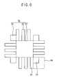
- FIG. 6 is an enlarged plan view illustrating one of the blocks shown in FIG. 5 .
- the unit block BL includes a body portion 10, a main branch 20 and a sub branch 30.
- the unit block BL may have a plurality of main branches 20 and a plurality of sub branches 30.
- the body portion 10 may have a substantially rectangular shape or a substantially square shape in a plan view.
- a plurality of main branches 20 may be extended from the sides of the body portion 10 in a horizontal direction and a longitudinal direction.
- Each of the main branches 20 has a substantially rectangular shape.
- Each of the sub branches 30 is protruded from each of the main branches 20 adjacent a corner region MA of the block BL toward the corner region MA.
- Each of the sub branches 30 may have a substantially rectangular shape or a substantially square shape.
- the corner region MA corresponds to each of the four corners of the block BL.
- the corner region MA may have a substantially rectangular shape or a substantially square shape.
- the number of the sub branches 30 may be four.
- an area of one of the sub branches 30 is about one-fourth of an area of the corner region MA, and four sub branches 30 of adjacent four blocks BL may be fitted to each other to fill the corner region MA.
- FIG. 7 is a plan view illustrating a plurality of light emitting diodes grouped into a plurality of blocks in accordance with an exemplary embodiment of the present invention.
- the blocks BL including a plurality of first blocks BL1 and a plurality of second blocks BL2, have substantially the same shape, that is, each of the first blocks BL1 has substantially the same shape as each of the second blocks BL2.
- Positions of the second blocks BL2 adjacent one of the first blocks BL1 have a rotation symmetry by about 60 degrees with respect to a center of the first block BL1, and are fitted to the first block BL1.
- each of the blocks BL has a substantially hexagonal shape, and each side of the hexagonal shape has an isosceles triangular saw-tooth shape.
- FIG. 8 is an enlarged plan view illustrating one of the blocks shown in FIG. 7 .
- each of the blocks BL has convex and concave shapes with respect to a hexagonal line HE of the block BL.
- Each of the convex and concave shapes has a substantially isosceles triangular shape, and has substantially the same area.
- the six sides of the block BL have substantially the same shape and size.
- FIGS. 1 to 8 four example blocks BL are described, however, the blocks BL may have various shapes.
- the sides of the adjacent blocks have the saw-tooth shape and are fitted to each other, so that the luminance is gradually changed on the interface between the adjacent blocks.
- image display quality of the display device may be improved.
- the luminance difference between the adjacent flat sided blocks may be seen on the interface between the sides of the straight line.
- the mixing area may be formed between the adjacent blocks so that the luminance in the mixing area may be between the luminance of a center of a bright block and the luminance of a center of a dark block.
Abstract
Description
- The present disclosure relates to a backlight assembly and a display device having the backlight assembly. More particularly, the present disclosure relates to a backlight assembly capable of improving an image display quality and a display device having the backlight assembly.
- A liquid crystal display (LCD) device, which is one of various kinds of flat panel display devices, displays an image by using electrical and optical characteristics of liquid crystals. The LCD device has various characteristics, such as small thickness, light weight, low power consumption, low driving voltage, and the like. Thus, the LCD device has been widely used as a display in various applications.
- The LCD device includes an LCD panel and a backlight assembly. The LCD panel displays an image using the light transmittance of the liquid crystals. The backlight assembly is disposed under the LCD panel to provide the LCD panel with light to be transmitted thereby.
- The LCD panel includes an array substrate, an opposite substrate and a liquid crystal layer. The array substrate includes a plurality of thin film transistors formed in a plurality of pixels. The opposite substrate includes a plurality of color filters. The liquid crystal layer is interposed between the array substrate and the opposite substrate. The color filters correspond to the pixels, respectively. The color filters include red color filter, green color filter, and a blue color filter.
- The backlight assembly includes a light source generating sufficient light so that the LCD panel can display the image. The light source can have various embodiments, such as a cold cathode fluorescent lamp (CCFL), a flat fluorescent lamp (FFL), a light emitting diode (LED), and the like.
- The light emitting diode can have various shapes, such as a chip shape and can have various characteristics, such as high luminance, low power consumption, and the like. Thus, the light emitting diode has been widely used as the light source of the backlight assembly for the LCD assembly. A plurality of light emitting diodes, in general, is disposed on a driving substrate, and includes a red light emitting diode, a green light emitting diode, and a blue light emitting diode.
- All of the light emitting diodes, in general, are turned on at the same time to generate the light. When all of the light emitting diodes are turned on, however, the lifetime of the light emitting diodes is decreased and a power consumption of the backlight assembly is increased.
- Also, when the light emitting diodes are individually operated to decrease the power consumption of the backlight assembly, an interface between a region in which the light emitting diodes are turned on and an adjacent region in which the light emitting diodes are turned off is displayed on the LCD panel as a straight line, thereby deteriorating an image display quality of the LCD device.
- Exemplary embodiments of the present invention provide a backlight assembly capable of improving an image display quality.
- Exemplary embodiments of the present invention also provide a display device having the above-mentioned backlight assembly.
- A backlight assembly in accordance with an exemplary embodiment of the present invention includes a plurality of blocks and a driving substrate.
- Each of the blocks includes a plurality of the light emitting diodes. The blocks may be independently operated. Sides of adjacent blocks are fitted to each other. The sides of the adjacent blocks may have a saw-tooth shape. The light emitting diodes are mounted on the driving substrate.
- The blocks may include a plurality of first blocks and a plurality of second blocks being adjacent the first blocks and fitted to the first blocks. Positions of the second blocks adjacent one of the first blocks may have a rotation symmetry with respect to a center of the first block by a constant rotation angle. The rotation angle may be about 90 degrees or about 60 degrees. Sides of each of the first and second blocks may have a substantially triangular saw-tooth shape or a substantially quadrangular saw-tooth shape.
- A display device in accordance with an exemplary embodiment of the present invention includes a backlight assembly and a display panel.
- The backlight assembly includes a plurality of blocks and a driving substrate on which the light emitting diodes are mounted. Each of the blocks includes a plurality of light emitting diodes, and the blocks may be independently operated. Sides of adjacent blocks are fitted to each other. The sides of the adjacent blocks may have a saw-tooth shape. The display panel is arranged on the backlight assembly in order to display an image.
- The display device may further include a controller unit electrically connected to the backlight assembly and the display panel to control the backlight assembly and the display panel.
- According to an exemplary embodiment of the present invention, the sides of the adjacent blocks have the saw-tooth shape and are fitted to each other, so that the luminance is gradually changed on the interface between the adjacent blocks. Thus, the image display quality of the display device is improved.
- Exemplary embodiments of the present invention will be understood in more detail from the following descriptions taken in conjunction with the accompanying drawings, in which:
-
FIG. 1 is an exploded perspective view illustrating a display device in accordance with an exemplary embodiment of the present invention; -
FIG. 2 is a plan view illustrating a plurality of light emitting diodes grouped into a plurality of blocks shown inFIG. 1 ; -
FIG. 3 is an enlarged plan view illustrating a first block and a second block inFIG. 2 adjacent each other; -
FIG. 4 is a plan view illustrating the block shown inFIG. 2 and a block in accordance with another exemplary embodiment of the present invention; -
FIG. 5 is a plan view illustrating a plurality of light emitting diodes grouped into a plurality of blocks in accordance with an exemplary embodiment of the present invention; -
FIG. 6 is an enlarged plan view illustrating the block shown inFIG. 5 ; -
FIG. 7 is a plan view illustrating a plurality of light emitting diodes grouped into a plurality of blocks in accordance with an exemplary embodiment of the present invention; and -
FIG. 8 is an enlarged plan view illustrating the block shown inFIG. 7 . - Exemplary embodiments of the present invention are described more fully hereinafter with reference to the accompanying drawings, in which the exemplary embodiments of the invention are shown. This invention may, however, be embodied in many different forms and should not be construed as limited to the exemplary embodiments set forth herein. Rather, these exemplary embodiments are provided so that this disclosure will be thorough and complete, and will fully convey the scope of the present invention to those of ordinary skill in the art.
-
FIG. 1 is an exploded perspective view illustrating a display device in accordance with an exemplary embodiment of the present invention. - Referring to
FIG. 1 , thedisplay device 400 includes adisplay panel 100, abacklight assembly 200 and acontroller unit 300. Thedisplay device 400 displays an image in accordance with image signals fed to thecontroller unit 300. - The
display panel 100 includes anarray substrate 110, anopposite substrate 120, aliquid crystal layer 130, a printedcircuit board 140, and aflexible circuit film 150. - Although not shown in
FIG. 1 , thearray substrate 110 includes a plurality of pixel electrodes, a plurality of thin film transistors and a plurality of signal lines. The pixel electrodes are arranged in a matrix shape, and include a transparent conductive material. The thin film transistors apply driving voltages to the pixel electrodes, respectively. The thin film transistors are turned on based on signals applied to the thin film transistors through the signal lines. - The signal lines include a plurality of gate lines and a plurality of data lines. The gate lines are extended in a direction different from an extended direction of the data lines. Each of the thin film transistors and each of the pixel electrodes are formed in each of the pixels.
- The
opposite substrate 120 faces thearray substrate 110. Although not shown inFIG. 1 , theopposite substrate 120 includes a common electrode and a plurality of color filters. The common electrode is formed on substantially the entire surface of theopposite substrate 120, and includes a transparent conductive material. The plurality of color filters correspond to the plurality of pixels, respectively. - The
liquid crystal layer 130 is interposed between thearray substrate 110 and theopposite substrate 120. Liquid crystals of theliquid crystal layer 130 vary their arrangement in response to an electric field applied thereto, and the light transmittance of theliquid crystal layer 130 is changed accordingly. - The printed
circuit board 140 converts an external control signal that is provided from an exterior to the printedcircuit board 140 into an image control signal. When theflexible circuit film 150 is bent backwardly, the printedcircuit board 140 is disposed under thearray substrate 110. Although not shown, the printedcircuit board 140 may include a data printed circuit board and a gate printed circuit board. On the other hand, an additional signal line may be formed on the array substrate and theflexible circuit film 150 so that the gate printed circuit may be omitted. - The printed
circuit board 140 is electrically connected to thearray substrate 110 through theflexible circuit film 150, so that the image control signal generated from the printedcircuit board 140 is applied to thearray substrate 110 through theflexible circuit film 150. Theflexible circuit film 150 may include a driving chip (not shown) that changes the image control signal into a driving signal for driving the thin film transistors (not shown). Although not shown, theflexible circuit film 150 may include a tape carrier package (TCP) or a chip on film (COF). Alternatively, the driving chip may not be formed on theflexible circuit film 150 but may be formed on thearray substrate 110. - The
backlight assembly 200 is disposed under thedisplay panel 100 to provide thedisplay panel 100 with light. Thebacklight assembly 200 includes abacklight assembly 210 that generates the light and a receivingcontainer 220 that receives thebacklight assembly 210. - The
backlight assembly 210 generates the light for thedisplay panel 100 to display an image. Thebacklight assembly 210 includes a drivingsubstrate 212 and a plurality oflight emitting diodes 214. - The driving
substrate 210 may further include a control line (not shown) and a power supply line (not shown). A control signal for controlling thelight emitting diodes 214 is applied to thelight emitting diodes 214 through the control line, and electric power is applied to thelight emitting diodes 214 through the power supply line. - The
light emitting diodes 214 are disposed on the drivingsubstrate 210 to generate the required light. Thelight emitting diodes 214 are electrically connected to the control line to receive the control signal for controlling them, and they are electrically connected to the power supply line to receive the electric power. - The
light emitting diodes 214 include a plurality of red light emitting diodes, a plurality of green light emitting diodes and a plurality of blue light emitting diodes. The red light emitting diodes generate red light. The green light emitting diodes generate green light. The blue light emitting diodes generate blue light. In addition, thelight emitting diodes 214 may further include a plurality of white light emitting diodes. - The
light emitting diodes 214 may be spaced apart from each other by a constant distance. In an exemplary embodiment, thelight emitting diodes 214 may be arranged in a matrix shape. InFIG. 1 , thelight emitting diodes 214 are driven by a local dimming method. In the local dimming method, thelight emitting diodes 214 are grouped into a plurality of blocks (BL), and the blocks are independently driven. - The receiving
container 220 may include abottom plate 222 and a plurality ofsidewalls 224 protruded from sides of thebottom plate 222 to form a receiving space. The receivingcontainer 220 receives thebacklight assembly 210. The receivingcontainer 220 may also receive thedisplay panel 100 on top of the backlight assembly. - The
backlight assembly 200 may further include optical sheets (not shown) that are interposed between thedisplay panel 100 and thebacklight assembly 210. Although not shown inFIG. 1 , the optical sheets may include a diffusion plate that increases luminance uniformity and at least one prism sheet that increases luminance when viewed at an angle. - The
controller unit 300 is electrically connected to thedisplay panel 100 and thebacklight assembly 210 to control thedisplay panel 100 and thebacklight assembly 210. Thecontroller unit 300 includes acontrolling circuit 310, a first connectingcable 320, a second connectingcable 330 and a third connectingcable 340. - In an exemplary embodiment, the controlling
circuit 310 is electrically connected to a main system (not shown), the printedcircuit board 140 of thedisplay panel 100 and thebacklight assembly 210 through the first connectingcable 320, the second connectingcable 330 and the third connectingcable 340, respectively. - The
controlling circuit 310 generates the image control signal and a light source control signal based on a circuit control signal that is fed from the main system (not shown). The image control signal is applied to thedisplay panel 100 to drive the thin film transistors in the pixels. The light source control signal is applied to thebacklight assembly 210 to independently drive thelight emitting diodes 214 in the blocks BL. - In
FIG. 1 , thebacklight assembly 210 is integrally formed with the drivingsubstrate 212 to drive thelight emitting diodes 214. Alternatively, thebacklight assembly 210 may include a plurality of driving substrates corresponding to the blocks, respectively. For example, each of the blocks BL may correspond to each of the driving substrates. -
FIG. 2 is a plan view illustrating a plurality of light emitting diodes grouped into a plurality of blocks as shown inFIG. 1 .FIG. 3 is an enlarged plan view illustrating a first block and a second block inFIG. 2 that are adjacent each other. - Referring to
FIGS. 2 and3 , thelight emitting diodes 214 are grouped into the blocks BL. The blocks BL are independently operated to generate the required light. - In an exemplary embodiment, each of the blocks BL has a saw-tooth edge shape so that the block BL is fitted to an adjacent block BL.
- Hereinafter, each of the blocks BL will be described, in detail.
- In an exemplary embodiment, the blocks BL includes a plurality of first blocks BL1 and a plurality of second blocks BL2. The second blocks BL2 are adjacent the first blocks BL1, and are fitted to the first blocks BL1. In an exemplary embodiment, each of the second blocks BL2 is adjacent each of the first blocks BL1 and is fitted to the adjacent first block BL1.
- In
FIG. 2 , positions of the second blocks BL2 adjacent one of the first blocks BL1 have a rotation symmetry with respect to a center of the first block BL1 by a constant rotation angle, and are fitted to the first block BL1. Also, positions of the first blocks BL1 adjacent one of the second blocks BL2 have a rotation symmetry with respect to a center of the second block BL2 by a constant rotation angle. - The rotation angle may be about 360/N degrees, wherein N is a natural number of no less than three. For example, the rotation angle may be about 120 degrees, about 90 degrees, about 72 degrees, about 60 degrees, about 51.4 degrees, or about 45 degrees. In an exemplary embodiment, the rotation angle may be about 90 degrees or about 60 degrees. When the rotation angle is about 90 degrees, the blocks BL form a substantially square shape or a substantially rectangular shape. Alternatively, when the rotation angle is about 60 degrees, the blocks BL form a substantially hexagonal shape. In
FIG. 2 , the rotation angle is about 90 degrees. - The first blocks BL1 may have substantially the same shape as the second blocks BL2. Alternatively, the first blocks BL1 may have a different shape from the second blocks BL2. In
FIGS. 2 and3 , the first block BL1 has a different shape from the second block BL2. - Sides of each of the first and second blocks BL1 and BL2 have a triangular saw-tooth shape or a quadrangular saw-tooth shape. Alternatively, the sides of each of the first and second blocks BL1 and BL2 may have a trapezoidal saw-tooth shape. In exemplary embodiments, the sides of each of the first and second blocks BL1 and BL2 have an isosceles triangular saw-tooth shape, a rectangular saw-tooth shape or an isosceles trapezoidal saw-tooth shape. In
FIG. 2 , the sides of each of the first and second blocks BL 1 and BL2 have the isosceles triangular saw-tooth shape. - In
FIG. 3 , the first block BL1 may have a different shape from the second block BL2. - Referring again to
FIG. 3 , positions of the second blocks BL2 adjacent the first block BL1 have a rotation symmetry with respect to the center of the first block BL1 by the rotation angle of about 90 degrees, and are fitted to the first block BL1. InFIG. 3 , although not shown, there would be three more second blocks BL2 adjacent the other sides. The blocks BL including the first and second blocks BL1 and BL2 form a rectangular shape or a square shape. In addition, the sides of each of the first and second blocks BL1 and BL2 have the triangular saw-tooth shape. - Corners of each of the first blocks BL 1 have different shapes from those of each of the second blocks BL2. The corners of each of the first blocks BL1 have a protruded shape, and the corners of each of the second blocks BL2 have a flat shape. In addition, the number of triangles formed on the sides of each of the first blocks BL1 is greater than the number of triangles formed on the sides of each of the second blocks BL2, that is, there are three corner triangles on first blocks BL1 and two corner triangles on second blocks BL2.
- The
light emitting diodes 214 are spaced apart from each other in each of the blocks BL, and a density of thelight emitting diodes 214 in each of the blocks BL is constant. - The
light emitting diodes 214 may be aligned along a central line CL crossing the centers of the adjacent first and second blocks BL1 and BL2. Alternatively, thelight emitting diodes 214 may be aligned in a direction substantially perpendicular to the central line CL crossing the centers of the adjacent first and second blocks BL1 and BL2. Thelight emitting diodes 214 may also be aligned in a direction inclined with respect to the central line CL crossing the centers of the adjacent first and second blocks BL1 and BL2. In an exemplary embodiment, the aligning direction of thelight emitting diodes 214 may form an angle of about 45 degrees with respect to the central line CL crossing the centers of the adjacent first and second blocks BL1 and BL2. - According to the display device shown in
FIGS. 1 to 3 , an interface between adjacent blocks BL has a saw-tooth shape, so that the luminance is gradually changed on the interface even though one of the blocks BL is turned on and the adjacent block BL is turned off. -
FIG. 4 is a plan view illustrating a part of the block shown inFIG. 2 and a block in accordance with a previously proposed construction. - Referring to
FIG. 4 , a luminance difference on an interface between adjacent blocks BL will be explained as follows. - Flat sided blocks BL' have a substantially rectangular shape or a substantially square shape, and an interface between adjacent flat sided blocks BL' has a linear shape as shown by the dashed line cruciform in
FIG. 4 . When one of the adjacent flat sided blocks BL' is turned on and a remainder of the adjacent flat sided blocks BL' are turned off, the interface between the adjacent flat sided blocks BL' is displayed as a line. - When each of blocks BL has a saw-tooth shape and adjacent blocks BL are fitted to each other, however, a mixing area is formed between the adjacent blocks BL. The mixing area is formed in a region in which sides of the adjacent blocks BL are fitted to each other.
- When light emitting
diodes 214 of the first blocks BL1 are turned on andlight emitting diodes 214 of the second blocks BL2 are turned off, the luminance of the mixing area is between the luminance of a center of the first block BL 1 and the luminance of a center of the second block BL2. Therefore, the luminance is gradually changed in the mixing area, so that the interface between the first and second blocks BL 1 and BL2 is not displayed. - When red, green and blue light emitting diodes are unequally arranged in the mixing area, color reproducibility of a display device may be deteriorated. In
FIG. 4 , however, white light emitting diodes are disposed in the mixing area, so that color reproducibility is increased, even though the white light emitting diodes are not equally arranged in the mixing area. -
FIG. 5 is a plan view illustrating a plurality of light emitting diodes grouped into a plurality of blocks in accordance with an exemplary embodiment of the present invention. The blocks ofFIG. 5 have a different shape from those shown inFIG. 2 . - Referring to
FIG. 5 , all of the blocks BL have substantially the same shape. In this exemplary embodiment, each of the first blocks BL1 has substantially the same shape as each of the second blocks BL2 that are adjacent the first blocks BL1. - Positions of the second blocks BL2 adjacent one of the first blocks BL1 have a rotation symmetry with respect to a center of the first block BL1 by about 90 degrees and are fitted to the first block BL1. Each of the blocks BL has a substantially rectangular shape or a substantially square shape. Also, sides of each of the blocks BL have a rectangular saw-tooth shape.
-
FIG. 6 is an enlarged plan view illustrating one of the blocks shown inFIG. 5 . - Referring to
FIG. 6 , the shape of each of the blocks BL will be described in detail. The unit block BL includes abody portion 10, amain branch 20 and asub branch 30. Alternatively, the unit block BL may have a plurality ofmain branches 20 and a plurality ofsub branches 30. - The
body portion 10 may have a substantially rectangular shape or a substantially square shape in a plan view. A plurality ofmain branches 20 may be extended from the sides of thebody portion 10 in a horizontal direction and a longitudinal direction. Each of themain branches 20 has a substantially rectangular shape. - Each of the
sub branches 30 is protruded from each of themain branches 20 adjacent a corner region MA of the block BL toward the corner region MA. Each of thesub branches 30 may have a substantially rectangular shape or a substantially square shape. - The corner region MA corresponds to each of the four corners of the block BL. The corner region MA may have a substantially rectangular shape or a substantially square shape. The number of the
sub branches 30 may be four. - In an exemplary embodiment, an area of one of the
sub branches 30 is about one-fourth of an area of the corner region MA, and foursub branches 30 of adjacent four blocks BL may be fitted to each other to fill the corner region MA. -
FIG. 7 is a plan view illustrating a plurality of light emitting diodes grouped into a plurality of blocks in accordance with an exemplary embodiment of the present invention. - Referring to
FIG. 7 , the blocks BL, including a plurality of first blocks BL1 and a plurality of second blocks BL2, have substantially the same shape, that is, each of the first blocks BL1 has substantially the same shape as each of the second blocks BL2. - Positions of the second blocks BL2 adjacent one of the first blocks BL1 have a rotation symmetry by about 60 degrees with respect to a center of the first block BL1, and are fitted to the first block BL1. In an exemplary embodiment, each of the blocks BL has a substantially hexagonal shape, and each side of the hexagonal shape has an isosceles triangular saw-tooth shape.
-
FIG. 8 is an enlarged plan view illustrating one of the blocks shown inFIG. 7 . - Referring to
FIG. 8 , the shape of each of the blocks BL will be described in detail. Each of the sides of the block BL has convex and concave shapes with respect to a hexagonal line HE of the block BL. Each of the convex and concave shapes has a substantially isosceles triangular shape, and has substantially the same area. In addition, the six sides of the block BL have substantially the same shape and size. - In
FIGS. 1 to 8 , four example blocks BL are described, however, the blocks BL may have various shapes. - According to exemplary embodiments of the present invention, the sides of the adjacent blocks have the saw-tooth shape and are fitted to each other, so that the luminance is gradually changed on the interface between the adjacent blocks. Thus, image display quality of the display device may be improved.
- When the sides of the adjacent flat sided blocks have a straight line, the luminance difference between the adjacent flat sided blocks may be seen on the interface between the sides of the straight line. When the sides of the adjacent blocks have the saw-tooth shape and are fitted to each other, however, the mixing area may be formed between the adjacent blocks so that the luminance in the mixing area may be between the luminance of a center of a bright block and the luminance of a center of a dark block. Thus, although the adjacent blocks are independently operated, the luminance is gradually changed between the adjacent blocks.
- The present invention has been described with reference to exemplary embodiments. It is evident, however, that many alternative modifications and variations will be apparent to those having ordinary skill in the art in light of the foregoing description. Accordingly, the present invention embraces all such alternative modifications and variations as fall within the spirit and scope of the appended claims.
Claims (20)
- A backlight assembly comprising:a plurality of blocks, each of the blocks including a plurality of light emitting diodes, sides of adjacent blocks being fitted to each other; anda driving substrate on which the plurality of light emitting diodes are mounted.
- The backlight assembly of claim 1, wherein the blocks are independently operated.
- The backlight assembly of claim 2, wherein positions of second blocks adjacent one of first blocks have a rotation symmetry with respect to a center of the first block by a constant rotation angle.
- The backlight assembly of claim 3, wherein the rotation angle is one of about 90 degrees and about 60 degrees.
- The backlight assembly of claim 3, wherein each of the plurality of first blocks and the plurality of second blocks have substantially the same shape.
- The backlight assembly of claim 5, wherein sides of each of the plurality of first blocks and the plurality of second blocks have a substantially triangular saw-tooth shape.
- The backlight assembly of claim 5, wherein sides of each of the plurality of first blocks and the plurality of second blocks have a substantially quadrangular saw-tooth shape.
- The backlight assembly of claim 3, wherein the plurality of first blocks have a different shape from the second blocks.
- The backlight assembly of claim 8, wherein positions of the second blocks adjacent one of the first blocks have a rotation symmetry by an angle of about 90 degrees with respect to a center of the first block, and
the sides of each of the plurality of first blocks and the plurality of second blocks have a substantially triangular saw-tooth shape. - The backlight assembly of claim 9, wherein the plurality of light emitting diodes are aligned in a direction forming an angle of about 45 degrees with respect to a central line crossing centers of adjacent first and second blocks.
- The backlight assembly of claim 1, wherein the driving substrate comprises a plurality of unit substrates corresponding to the plurality of blocks, respectively.
- The backlight assembly of claim 1, wherein the plurality of light emitting diodes comprise a plurality of red light emitting diodes, a plurality of green light emitting diodes and a plurality of blue light emitting diodes.
- The backlight assembly of claim 1, wherein the plurality of light emitting diodes comprise a plurality of white light emitting diodes.
- A display device comprising:a backlight assembly including:a display panel arranged on the backlight assembly to display an image.a plurality of blocks, each of the blocks including a plurality of light emitting diodes, sides of adjacent blocks being fitted to each other; anda driving substrate on which the plurality of light emitting diodes are mounted; and
- The display device of claim 14, further comprising a controller unit electrically connected to the backlight assembly and the display panel to control the backlight assembly and the display panel.
- The display device of claim 14, wherein the blocks are independently operated.
- The display device of claim 14, wherein the display panel comprises:an array substrate including a thin film transistor;an opposite substrate facing the array substrate; anda liquid crystal layer interposed between the array substrate and the opposite substrate.
- The display device of claim 14, wherein the plurality of blocks comprises:a plurality of first blocks; anda plurality of second blocks adjacent the first blocks and fitted to the first blocks.
- The display device of claim 18, wherein positions of the second blocks adjacent one of the first blocks have a rotation symmetry by a constant rotation angle with respect to a center of the first block.
- The display device of claim 19, wherein the rotation angle is one of about 90 degrees and about 60 degrees.
Applications Claiming Priority (1)
| Application Number | Priority Date | Filing Date | Title |
|---|---|---|---|
| KR1020060122737A KR20080051499A (en) | 2006-12-06 | 2006-12-06 | Light module and display apparatus having the same |
Publications (1)
| Publication Number | Publication Date |
|---|---|
| EP1930947A1 true EP1930947A1 (en) | 2008-06-11 |
Family
ID=39144322
Family Applications (1)
| Application Number | Title | Priority Date | Filing Date |
|---|---|---|---|
| EP07022441A Withdrawn EP1930947A1 (en) | 2006-12-06 | 2007-11-20 | Backlight assembly and display device having the same |
Country Status (5)
| Country | Link |
|---|---|
| US (1) | US20080137336A1 (en) |
| EP (1) | EP1930947A1 (en) |
| JP (1) | JP2008147187A (en) |
| KR (1) | KR20080051499A (en) |
| CN (1) | CN101196650A (en) |
Cited By (9)
| Publication number | Priority date | Publication date | Assignee | Title |
|---|---|---|---|---|
| WO2009012914A1 (en) * | 2007-07-26 | 2009-01-29 | Osram Gesellschaft mit beschränkter Haftung | Illumination device |
| WO2009138924A1 (en) * | 2008-05-13 | 2009-11-19 | Koninklijke Philips Electronics N.V. | Arrangement to avoid sharp luminance edges in a segmented light output device |
| WO2010014578A1 (en) * | 2008-07-31 | 2010-02-04 | Solid State Opto Limited | Optically transmissive substrates and light emitting assemblies and methods of making same, and methods of displaying images using the optically transmissive substrates and light emitting assemblies |
| WO2011101172A3 (en) * | 2010-02-22 | 2012-03-15 | Epiq Gmbh | Light source having led arrays for direct operation in an alternating current network and production method therefor |
| EP2508789A1 (en) * | 2009-12-02 | 2012-10-10 | Sharp Kabushiki Kaisha | Illumination device, and display device |
| EP2690343A1 (en) | 2012-07-25 | 2014-01-29 | Trilux GmbH & Co. KG | Luminaire for mixing coloured lights, in particular of ww and tw light from LED elements, and LED module therefor |
| EP2640171A3 (en) * | 2012-01-30 | 2014-03-05 | Siteco Beleuchtungstechnik GmbH | Circuit board with a regular LED assembly |
| US9563007B2 (en) | 2011-10-20 | 2017-02-07 | Rambus Delaware Llc | Modular light-emitting panel assembly |
| WO2018114470A1 (en) | 2016-12-21 | 2018-06-28 | Lumileds Holding B.V. | Aligned arrangement of leds |
Families Citing this family (17)
| Publication number | Priority date | Publication date | Assignee | Title |
|---|---|---|---|---|
| WO2009020021A1 (en) * | 2007-08-09 | 2009-02-12 | Nec Lighting, Ltd. | Illuminating device |
| WO2010047164A1 (en) * | 2008-10-22 | 2010-04-29 | シャープ株式会社 | Illuminating device, display device and television receiver |
| CN101408296B (en) * | 2008-10-24 | 2013-02-27 | 李鑫 | LED apparatus |
| KR20100074740A (en) * | 2008-12-24 | 2010-07-02 | 삼성전자주식회사 | Electronic apparatus and backlight unit for electronic apparatus |
| KR101521098B1 (en) * | 2009-01-06 | 2015-05-20 | 삼성디스플레이 주식회사 | Method of driving a light-source and light-source apparatus for performing the method |
| JP5386238B2 (en) * | 2009-06-04 | 2014-01-15 | 株式会社日立ハイテクノロジーズ | Panel substrate transfer device and display panel module assembly device |
| KR101580921B1 (en) | 2009-08-14 | 2015-12-30 | 삼성디스플레이 주식회사 | Display apparatus |
| WO2011067978A1 (en) * | 2009-12-02 | 2011-06-09 | シャープ株式会社 | Illumination device and display device |
| CN102456317A (en) * | 2010-10-19 | 2012-05-16 | 昆达电脑科技(昆山)有限公司 | Display screen with adjustable partial backlights |
| CN102384409B (en) * | 2011-11-18 | 2016-03-23 | 深圳市华星光电技术有限公司 | Back light system |
| CN102376214B (en) * | 2011-11-18 | 2014-08-06 | 深圳市华星光电技术有限公司 | Flat-panel display device and stereoscopic display device |
| WO2014002085A1 (en) | 2012-06-26 | 2014-01-03 | M.N. Wasserman Ltd. | A modular light system |
| CN108681148A (en) * | 2018-04-28 | 2018-10-19 | 珠海晨新科技有限公司 | A kind of LED backlight and LED display |
| CN108535917A (en) * | 2018-04-28 | 2018-09-14 | 珠海晨新科技有限公司 | A kind of design method of LED backlight and LED screen |
| CN109521603A (en) * | 2018-12-10 | 2019-03-26 | 厦门天马微电子有限公司 | Backlight module and display device |
| KR20200127648A (en) * | 2019-05-03 | 2020-11-11 | 엘지전자 주식회사 | Display device |
| CN115933248B (en) * | 2022-10-21 | 2024-01-26 | 惠科股份有限公司 | Backlight module and display device |
Citations (4)
| Publication number | Priority date | Publication date | Assignee | Title |
|---|---|---|---|---|
| DE19914281C1 (en) * | 1999-03-30 | 2000-03-16 | Andreas Toeteberg | Light emitting module for combining and fusing to other light emitting modules of equal type; has connector devices in external casing areas and electrical contacts that can be fixed to contacts with other modules |
| US20010024368A1 (en) * | 2000-03-16 | 2001-09-27 | Bjb Gmbh & Co. Kg | Modular led assembly |
| US20060012993A1 (en) * | 2004-07-16 | 2006-01-19 | Enplas Corporation | Surface light source device, illumination unit and light flux control member |
| EP1881362A1 (en) * | 2006-07-21 | 2008-01-23 | Sony Corporation | Light source module, light source apparatus and liquid crystal display |
-
2006
- 2006-12-06 KR KR1020060122737A patent/KR20080051499A/en not_active Application Discontinuation
-
2007
- 2007-10-31 US US11/930,872 patent/US20080137336A1/en not_active Abandoned
- 2007-11-20 EP EP07022441A patent/EP1930947A1/en not_active Withdrawn
- 2007-12-04 JP JP2007313005A patent/JP2008147187A/en active Pending
- 2007-12-06 CN CNA2007101967712A patent/CN101196650A/en active Pending
Patent Citations (4)
| Publication number | Priority date | Publication date | Assignee | Title |
|---|---|---|---|---|
| DE19914281C1 (en) * | 1999-03-30 | 2000-03-16 | Andreas Toeteberg | Light emitting module for combining and fusing to other light emitting modules of equal type; has connector devices in external casing areas and electrical contacts that can be fixed to contacts with other modules |
| US20010024368A1 (en) * | 2000-03-16 | 2001-09-27 | Bjb Gmbh & Co. Kg | Modular led assembly |
| US20060012993A1 (en) * | 2004-07-16 | 2006-01-19 | Enplas Corporation | Surface light source device, illumination unit and light flux control member |
| EP1881362A1 (en) * | 2006-07-21 | 2008-01-23 | Sony Corporation | Light source module, light source apparatus and liquid crystal display |
Non-Patent Citations (1)
| Title |
|---|
| SHIRAI T ET AL: "RGB-LED backlights for LCD-TVs with 0D, 1D, and 2D adaptive dimming", DIG. TECH. PAP. SID INT. SYMP.; DIGEST OF TECHNICAL PAPERS - SID INTERNATIONAL SYMPOSIUM; SOCIETY FOR INFORMATION DISPLAY - 44TH INTERNATIONAL SYMPOSIUM, SEMINAR, AND EXHIBITION, SID 2006 - INTERNATIONAL SYMPOSIUM DIGEST OF TECHNICAL PAPERS 2006, vol. 37, no. 4, 2006 - June 2006 (2006-06-01), pages 1495 - 1498, XP002472082 * |
Cited By (16)
| Publication number | Priority date | Publication date | Assignee | Title |
|---|---|---|---|---|
| WO2009012914A1 (en) * | 2007-07-26 | 2009-01-29 | Osram Gesellschaft mit beschränkter Haftung | Illumination device |
| WO2009138924A1 (en) * | 2008-05-13 | 2009-11-19 | Koninklijke Philips Electronics N.V. | Arrangement to avoid sharp luminance edges in a segmented light output device |
| WO2010014578A1 (en) * | 2008-07-31 | 2010-02-04 | Solid State Opto Limited | Optically transmissive substrates and light emitting assemblies and methods of making same, and methods of displaying images using the optically transmissive substrates and light emitting assemblies |
| US8462292B2 (en) | 2008-07-31 | 2013-06-11 | Rambus Delaware Llc | Optically transmissive substrates and light emitting assemblies and methods of making same, and methods of displaying images using the optically transmissive substrates and light emitting assemblies |
| EP2508789A1 (en) * | 2009-12-02 | 2012-10-10 | Sharp Kabushiki Kaisha | Illumination device, and display device |
| EP2508789A4 (en) * | 2009-12-02 | 2013-12-04 | Sharp Kk | Illumination device, and display device |
| US8937432B2 (en) | 2010-02-22 | 2015-01-20 | Integrated Micro-Electronics Bulgaria | Light source having LED arrays for direct operation in alternating current network and production method therefor |
| WO2011101172A3 (en) * | 2010-02-22 | 2012-03-15 | Epiq Gmbh | Light source having led arrays for direct operation in an alternating current network and production method therefor |
| US9563007B2 (en) | 2011-10-20 | 2017-02-07 | Rambus Delaware Llc | Modular light-emitting panel assembly |
| US9772440B2 (en) | 2011-10-20 | 2017-09-26 | Rambus Delaware Llc | Modular light-emitting panel assembly |
| EP2640171A3 (en) * | 2012-01-30 | 2014-03-05 | Siteco Beleuchtungstechnik GmbH | Circuit board with a regular LED assembly |
| DE102012213046A1 (en) * | 2012-07-25 | 2014-01-30 | Trilux Gmbh & Co. Kg | Luminaire for mixing light colors, in particular ww and tw light from LED elements, as well as circuit board and LED module therefor |
| EP2690343B1 (en) | 2012-07-25 | 2016-01-06 | Trilux GmbH & Co. KG | Luminaire for mixing coloured lights, in particular of ww and tw light from LED elements, and LED module therefor |
| EP2690343A1 (en) | 2012-07-25 | 2014-01-29 | Trilux GmbH & Co. KG | Luminaire for mixing coloured lights, in particular of ww and tw light from LED elements, and LED module therefor |
| WO2018114470A1 (en) | 2016-12-21 | 2018-06-28 | Lumileds Holding B.V. | Aligned arrangement of leds |
| US10734364B2 (en) | 2016-12-21 | 2020-08-04 | Lumileds Llc | Aligned arrangement of LEDs |
Also Published As
| Publication number | Publication date |
|---|---|
| CN101196650A (en) | 2008-06-11 |
| US20080137336A1 (en) | 2008-06-12 |
| KR20080051499A (en) | 2008-06-11 |
| JP2008147187A (en) | 2008-06-26 |
Similar Documents
| Publication | Publication Date | Title |
|---|---|---|
| EP1930947A1 (en) | Backlight assembly and display device having the same | |
| CN100501546C (en) | Display device | |
| US7585083B2 (en) | Backlight for display device | |
| US7530711B2 (en) | Backlight assembly and liquid crystal display module using the same | |
| US7259810B2 (en) | Backlight assembly having particular lamp and reflecting plate arrangement and direct lighting type liquid crystal display apparatus | |
| JP5066572B2 (en) | Backlight unit and liquid crystal display device including the same | |
| EP2192440B1 (en) | Liquid crystal display | |
| US7306357B2 (en) | Line light source using light emitting diode and lens and backlight unit using the same | |
| EP1901112B1 (en) | Backlight assembly and display apparatus having the same | |
| US20080144334A1 (en) | Light emitting diode package, and light source unit and backlight unit including the same | |
| US20070188677A1 (en) | Backlight assembly and display device including the same | |
| US20080074902A1 (en) | Lcd backlight assembly with leds | |
| US8054402B2 (en) | Optical member, backlight assembly and display apparatus having the same | |
| KR20170076214A (en) | Backlight unit and liquid crystal dispaly device including the same | |
| US20070171669A1 (en) | Backlight assembly and liquid crystal display device having the same | |
| US20140009695A1 (en) | Illumination device, display device, and television reception device | |
| US9588280B2 (en) | Backlight assembly and display apparatus including the same | |
| US20120175650A1 (en) | Illuminating device and display device | |
| US9476577B2 (en) | Lighting device, display device, and television reception device | |
| KR101158904B1 (en) | Display device | |
| KR20060095144A (en) | Light emitting diodes back-light assembly and liquid crystal display device module using thereof | |
| KR20060028104A (en) | Light generating device, back-light assembly having the light generating device and display apparatus having the back-light assembly | |
| KR20080101501A (en) | Diffusion plate and liquid crystal display including the same | |
| KR20080039630A (en) | Liquid crystal display device | |
| KR101510907B1 (en) | Backlight unit and liquid crystal display device having the same |
Legal Events
| Date | Code | Title | Description |
|---|---|---|---|
| PUAI | Public reference made under article 153(3) epc to a published international application that has entered the european phase |
Free format text: ORIGINAL CODE: 0009012 |
|
| AK | Designated contracting states |
Kind code of ref document: A1 Designated state(s): AT BE BG CH CY CZ DE DK EE ES FI FR GB GR HU IE IS IT LI LT LU LV MC MT NL PL PT RO SE SI SK TR |
|
| AX | Request for extension of the european patent |
Extension state: AL BA HR MK RS |
|
| 17P | Request for examination filed |
Effective date: 20081122 |
|
| 17Q | First examination report despatched |
Effective date: 20090108 |
|
| AKX | Designation fees paid |
Designated state(s): DE FR GB IT |
|
| STAA | Information on the status of an ep patent application or granted ep patent |
Free format text: STATUS: THE APPLICATION HAS BEEN WITHDRAWN |
|
| 18W | Application withdrawn |
Effective date: 20090414 |