EP1876524B1 - General purpose, programmable media processor executing groups floating point instructions - Google Patents
General purpose, programmable media processor executing groups floating point instructions Download PDFInfo
- Publication number
- EP1876524B1 EP1876524B1 EP07111351A EP07111351A EP1876524B1 EP 1876524 B1 EP1876524 B1 EP 1876524B1 EP 07111351 A EP07111351 A EP 07111351A EP 07111351 A EP07111351 A EP 07111351A EP 1876524 B1 EP1876524 B1 EP 1876524B1
- Authority
- EP
- European Patent Office
- Prior art keywords
- register
- data elements
- data
- floating point
- instruction
- Prior art date
- Legal status (The legal status is an assumption and is not a legal conclusion. Google has not performed a legal analysis and makes no representation as to the accuracy of the status listed.)
- Expired - Lifetime
Links
- 238000007667 floating Methods 0.000 title claims abstract description 54
- 238000012545 processing Methods 0.000 claims abstract description 36
- 238000005192 partition Methods 0.000 claims description 26
- 230000004044 response Effects 0.000 claims description 16
- 230000002441 reversible effect Effects 0.000 claims description 3
- 238000000034 method Methods 0.000 abstract description 30
- 230000008569 process Effects 0.000 abstract description 12
- 230000007175 bidirectional communication Effects 0.000 abstract description 6
- 230000006855 networking Effects 0.000 abstract description 4
- 238000000638 solvent extraction Methods 0.000 abstract description 2
- 230000015654 memory Effects 0.000 description 171
- 230000006854 communication Effects 0.000 description 83
- 238000004891 communication Methods 0.000 description 83
- 239000000872 buffer Substances 0.000 description 40
- 230000005540 biological transmission Effects 0.000 description 27
- 238000007726 management method Methods 0.000 description 19
- 238000001228 spectrum Methods 0.000 description 16
- 238000010586 diagram Methods 0.000 description 12
- 238000013459 approach Methods 0.000 description 11
- 239000000835 fiber Substances 0.000 description 11
- 230000006870 function Effects 0.000 description 11
- 230000000007 visual effect Effects 0.000 description 8
- 238000004364 calculation method Methods 0.000 description 6
- 239000004744 fabric Substances 0.000 description 6
- 238000012546 transfer Methods 0.000 description 6
- 230000007246 mechanism Effects 0.000 description 5
- 238000007792 addition Methods 0.000 description 4
- 230000008901 benefit Effects 0.000 description 4
- 238000007906 compression Methods 0.000 description 4
- 230000006835 compression Effects 0.000 description 4
- 238000005516 engineering process Methods 0.000 description 4
- 230000002093 peripheral effect Effects 0.000 description 4
- 238000011144 upstream manufacturing Methods 0.000 description 4
- 238000012937 correction Methods 0.000 description 3
- 230000008878 coupling Effects 0.000 description 3
- 238000010168 coupling process Methods 0.000 description 3
- 238000005859 coupling reaction Methods 0.000 description 3
- 238000013144 data compression Methods 0.000 description 3
- 238000013478 data encryption standard Methods 0.000 description 3
- 238000009434 installation Methods 0.000 description 3
- 230000000630 rising effect Effects 0.000 description 3
- 230000003068 static effect Effects 0.000 description 3
- 238000013519 translation Methods 0.000 description 3
- RYGMFSIKBFXOCR-UHFFFAOYSA-N Copper Chemical compound [Cu] RYGMFSIKBFXOCR-UHFFFAOYSA-N 0.000 description 2
- XUIMIQQOPSSXEZ-UHFFFAOYSA-N Silicon Chemical compound [Si] XUIMIQQOPSSXEZ-UHFFFAOYSA-N 0.000 description 2
- 229910052802 copper Inorganic materials 0.000 description 2
- 239000010949 copper Substances 0.000 description 2
- 230000006735 deficit Effects 0.000 description 2
- 230000001419 dependent effect Effects 0.000 description 2
- 238000013461 design Methods 0.000 description 2
- 235000019800 disodium phosphate Nutrition 0.000 description 2
- 239000003999 initiator Substances 0.000 description 2
- 238000012986 modification Methods 0.000 description 2
- 230000004048 modification Effects 0.000 description 2
- 239000013307 optical fiber Substances 0.000 description 2
- 230000009467 reduction Effects 0.000 description 2
- 230000002829 reductive effect Effects 0.000 description 2
- 230000008672 reprogramming Effects 0.000 description 2
- 239000004065 semiconductor Substances 0.000 description 2
- 229910052710 silicon Inorganic materials 0.000 description 2
- 239000010703 silicon Substances 0.000 description 2
- 230000002459 sustained effect Effects 0.000 description 2
- 230000001360 synchronised effect Effects 0.000 description 2
- 101150012579 ADSL gene Proteins 0.000 description 1
- 102100020775 Adenylosuccinate lyase Human genes 0.000 description 1
- 108700040193 Adenylosuccinate lyases Proteins 0.000 description 1
- 239000012572 advanced medium Substances 0.000 description 1
- 230000003321 amplification Effects 0.000 description 1
- 230000003190 augmentative effect Effects 0.000 description 1
- 230000001413 cellular effect Effects 0.000 description 1
- 239000000470 constituent Substances 0.000 description 1
- 230000001934 delay Effects 0.000 description 1
- 230000003111 delayed effect Effects 0.000 description 1
- 238000001514 detection method Methods 0.000 description 1
- 238000002592 echocardiography Methods 0.000 description 1
- 230000000694 effects Effects 0.000 description 1
- 230000002708 enhancing effect Effects 0.000 description 1
- 238000001914 filtration Methods 0.000 description 1
- RGNPBRKPHBKNKX-UHFFFAOYSA-N hexaflumuron Chemical compound C1=C(Cl)C(OC(F)(F)C(F)F)=C(Cl)C=C1NC(=O)NC(=O)C1=C(F)C=CC=C1F RGNPBRKPHBKNKX-UHFFFAOYSA-N 0.000 description 1
- 238000010348 incorporation Methods 0.000 description 1
- 238000003780 insertion Methods 0.000 description 1
- 230000037431 insertion Effects 0.000 description 1
- 230000002452 interceptive effect Effects 0.000 description 1
- 230000000670 limiting effect Effects 0.000 description 1
- 238000007620 mathematical function Methods 0.000 description 1
- 239000002609 medium Substances 0.000 description 1
- 238000006386 neutralization reaction Methods 0.000 description 1
- 238000003199 nucleic acid amplification method Methods 0.000 description 1
- 230000008520 organization Effects 0.000 description 1
- 230000010363 phase shift Effects 0.000 description 1
- 238000012552 review Methods 0.000 description 1
- 230000001953 sensory effect Effects 0.000 description 1
- 230000011664 signaling Effects 0.000 description 1
- 238000004513 sizing Methods 0.000 description 1
- 238000012360 testing method Methods 0.000 description 1
- 230000007704 transition Effects 0.000 description 1
- 238000000411 transmission spectrum Methods 0.000 description 1
Images


Classifications
-
- G—PHYSICS
- G06—COMPUTING; CALCULATING OR COUNTING
- G06F—ELECTRIC DIGITAL DATA PROCESSING
- G06F9/00—Arrangements for program control, e.g. control units
- G06F9/06—Arrangements for program control, e.g. control units using stored programs, i.e. using an internal store of processing equipment to receive or retain programs
- G06F9/30—Arrangements for executing machine instructions, e.g. instruction decode
- G06F9/38—Concurrent instruction execution, e.g. pipeline, look ahead
- G06F9/3802—Instruction prefetching
-
- G—PHYSICS
- G06—COMPUTING; CALCULATING OR COUNTING
- G06F—ELECTRIC DIGITAL DATA PROCESSING
- G06F12/00—Accessing, addressing or allocating within memory systems or architectures
- G06F12/02—Addressing or allocation; Relocation
- G06F12/08—Addressing or allocation; Relocation in hierarchically structured memory systems, e.g. virtual memory systems
- G06F12/0802—Addressing of a memory level in which the access to the desired data or data block requires associative addressing means, e.g. caches
- G06F12/0875—Addressing of a memory level in which the access to the desired data or data block requires associative addressing means, e.g. caches with dedicated cache, e.g. instruction or stack
-
- G—PHYSICS
- G06—COMPUTING; CALCULATING OR COUNTING
- G06F—ELECTRIC DIGITAL DATA PROCESSING
- G06F12/00—Accessing, addressing or allocating within memory systems or architectures
- G06F12/02—Addressing or allocation; Relocation
- G06F12/08—Addressing or allocation; Relocation in hierarchically structured memory systems, e.g. virtual memory systems
- G06F12/10—Address translation
- G06F12/1027—Address translation using associative or pseudo-associative address translation means, e.g. translation look-aside buffer [TLB]
-
- G—PHYSICS
- G06—COMPUTING; CALCULATING OR COUNTING
- G06F—ELECTRIC DIGITAL DATA PROCESSING
- G06F15/00—Digital computers in general; Data processing equipment in general
- G06F15/76—Architectures of general purpose stored program computers
- G06F15/78—Architectures of general purpose stored program computers comprising a single central processing unit
- G06F15/7828—Architectures of general purpose stored program computers comprising a single central processing unit without memory
- G06F15/7832—Architectures of general purpose stored program computers comprising a single central processing unit without memory on one IC chip (single chip microprocessors)
-
- G—PHYSICS
- G06—COMPUTING; CALCULATING OR COUNTING
- G06F—ELECTRIC DIGITAL DATA PROCESSING
- G06F15/00—Digital computers in general; Data processing equipment in general
- G06F15/76—Architectures of general purpose stored program computers
- G06F15/78—Architectures of general purpose stored program computers comprising a single central processing unit
- G06F15/7839—Architectures of general purpose stored program computers comprising a single central processing unit with memory
- G06F15/7842—Architectures of general purpose stored program computers comprising a single central processing unit with memory on one IC chip (single chip microcontrollers)
-
- G—PHYSICS
- G06—COMPUTING; CALCULATING OR COUNTING
- G06F—ELECTRIC DIGITAL DATA PROCESSING
- G06F9/00—Arrangements for program control, e.g. control units
- G06F9/06—Arrangements for program control, e.g. control units using stored programs, i.e. using an internal store of processing equipment to receive or retain programs
- G06F9/30—Arrangements for executing machine instructions, e.g. instruction decode
- G06F9/30003—Arrangements for executing specific machine instructions
- G06F9/30007—Arrangements for executing specific machine instructions to perform operations on data operands
- G06F9/3001—Arithmetic instructions
- G06F9/30014—Arithmetic instructions with variable precision
-
- G—PHYSICS
- G06—COMPUTING; CALCULATING OR COUNTING
- G06F—ELECTRIC DIGITAL DATA PROCESSING
- G06F9/00—Arrangements for program control, e.g. control units
- G06F9/06—Arrangements for program control, e.g. control units using stored programs, i.e. using an internal store of processing equipment to receive or retain programs
- G06F9/30—Arrangements for executing machine instructions, e.g. instruction decode
- G06F9/30003—Arrangements for executing specific machine instructions
- G06F9/30007—Arrangements for executing specific machine instructions to perform operations on data operands
- G06F9/30018—Bit or string instructions
-
- G—PHYSICS
- G06—COMPUTING; CALCULATING OR COUNTING
- G06F—ELECTRIC DIGITAL DATA PROCESSING
- G06F9/00—Arrangements for program control, e.g. control units
- G06F9/06—Arrangements for program control, e.g. control units using stored programs, i.e. using an internal store of processing equipment to receive or retain programs
- G06F9/30—Arrangements for executing machine instructions, e.g. instruction decode
- G06F9/30003—Arrangements for executing specific machine instructions
- G06F9/30007—Arrangements for executing specific machine instructions to perform operations on data operands
- G06F9/30025—Format conversion instructions, e.g. Floating-Point to Integer, decimal conversion
-
- G—PHYSICS
- G06—COMPUTING; CALCULATING OR COUNTING
- G06F—ELECTRIC DIGITAL DATA PROCESSING
- G06F9/00—Arrangements for program control, e.g. control units
- G06F9/06—Arrangements for program control, e.g. control units using stored programs, i.e. using an internal store of processing equipment to receive or retain programs
- G06F9/30—Arrangements for executing machine instructions, e.g. instruction decode
- G06F9/30003—Arrangements for executing specific machine instructions
- G06F9/30007—Arrangements for executing specific machine instructions to perform operations on data operands
- G06F9/30032—Movement instructions, e.g. MOVE, SHIFT, ROTATE, SHUFFLE
-
- G—PHYSICS
- G06—COMPUTING; CALCULATING OR COUNTING
- G06F—ELECTRIC DIGITAL DATA PROCESSING
- G06F9/00—Arrangements for program control, e.g. control units
- G06F9/06—Arrangements for program control, e.g. control units using stored programs, i.e. using an internal store of processing equipment to receive or retain programs
- G06F9/30—Arrangements for executing machine instructions, e.g. instruction decode
- G06F9/30003—Arrangements for executing specific machine instructions
- G06F9/30007—Arrangements for executing specific machine instructions to perform operations on data operands
- G06F9/30036—Instructions to perform operations on packed data, e.g. vector, tile or matrix operations
-
- G—PHYSICS
- G06—COMPUTING; CALCULATING OR COUNTING
- G06F—ELECTRIC DIGITAL DATA PROCESSING
- G06F9/00—Arrangements for program control, e.g. control units
- G06F9/06—Arrangements for program control, e.g. control units using stored programs, i.e. using an internal store of processing equipment to receive or retain programs
- G06F9/30—Arrangements for executing machine instructions, e.g. instruction decode
- G06F9/30003—Arrangements for executing specific machine instructions
- G06F9/3004—Arrangements for executing specific machine instructions to perform operations on memory
- G06F9/30043—LOAD or STORE instructions; Clear instruction
-
- G—PHYSICS
- G06—COMPUTING; CALCULATING OR COUNTING
- G06F—ELECTRIC DIGITAL DATA PROCESSING
- G06F9/00—Arrangements for program control, e.g. control units
- G06F9/06—Arrangements for program control, e.g. control units using stored programs, i.e. using an internal store of processing equipment to receive or retain programs
- G06F9/30—Arrangements for executing machine instructions, e.g. instruction decode
- G06F9/30003—Arrangements for executing specific machine instructions
- G06F9/30072—Arrangements for executing specific machine instructions to perform conditional operations, e.g. using predicates or guards
-
- G—PHYSICS
- G06—COMPUTING; CALCULATING OR COUNTING
- G06F—ELECTRIC DIGITAL DATA PROCESSING
- G06F9/00—Arrangements for program control, e.g. control units
- G06F9/06—Arrangements for program control, e.g. control units using stored programs, i.e. using an internal store of processing equipment to receive or retain programs
- G06F9/30—Arrangements for executing machine instructions, e.g. instruction decode
- G06F9/30003—Arrangements for executing specific machine instructions
- G06F9/30076—Arrangements for executing specific machine instructions to perform miscellaneous control operations, e.g. NOP
- G06F9/30087—Synchronisation or serialisation instructions
-
- G—PHYSICS
- G06—COMPUTING; CALCULATING OR COUNTING
- G06F—ELECTRIC DIGITAL DATA PROCESSING
- G06F9/00—Arrangements for program control, e.g. control units
- G06F9/06—Arrangements for program control, e.g. control units using stored programs, i.e. using an internal store of processing equipment to receive or retain programs
- G06F9/30—Arrangements for executing machine instructions, e.g. instruction decode
- G06F9/30145—Instruction analysis, e.g. decoding, instruction word fields
-
- G—PHYSICS
- G06—COMPUTING; CALCULATING OR COUNTING
- G06F—ELECTRIC DIGITAL DATA PROCESSING
- G06F9/00—Arrangements for program control, e.g. control units
- G06F9/06—Arrangements for program control, e.g. control units using stored programs, i.e. using an internal store of processing equipment to receive or retain programs
- G06F9/30—Arrangements for executing machine instructions, e.g. instruction decode
- G06F9/38—Concurrent instruction execution, e.g. pipeline, look ahead
- G06F9/3867—Concurrent instruction execution, e.g. pipeline, look ahead using instruction pipelines
- G06F9/3869—Implementation aspects, e.g. pipeline latches; pipeline synchronisation and clocking
-
- H—ELECTRICITY
- H04—ELECTRIC COMMUNICATION TECHNIQUE
- H04N—PICTORIAL COMMUNICATION, e.g. TELEVISION
- H04N21/00—Selective content distribution, e.g. interactive television or video on demand [VOD]
- H04N21/20—Servers specifically adapted for the distribution of content, e.g. VOD servers; Operations thereof
- H04N21/23—Processing of content or additional data; Elementary server operations; Server middleware
- H04N21/236—Assembling of a multiplex stream, e.g. transport stream, by combining a video stream with other content or additional data, e.g. inserting a URL [Uniform Resource Locator] into a video stream, multiplexing software data into a video stream; Remultiplexing of multiplex streams; Insertion of stuffing bits into the multiplex stream, e.g. to obtain a constant bit-rate; Assembling of a packetised elementary stream
- H04N21/2365—Multiplexing of several video streams
-
- H—ELECTRICITY
- H04—ELECTRIC COMMUNICATION TECHNIQUE
- H04N—PICTORIAL COMMUNICATION, e.g. TELEVISION
- H04N21/00—Selective content distribution, e.g. interactive television or video on demand [VOD]
- H04N21/20—Servers specifically adapted for the distribution of content, e.g. VOD servers; Operations thereof
- H04N21/23—Processing of content or additional data; Elementary server operations; Server middleware
- H04N21/238—Interfacing the downstream path of the transmission network, e.g. adapting the transmission rate of a video stream to network bandwidth; Processing of multiplex streams
- H04N21/23805—Controlling the feeding rate to the network, e.g. by controlling the video pump
-
- H—ELECTRICITY
- H04—ELECTRIC COMMUNICATION TECHNIQUE
- H04N—PICTORIAL COMMUNICATION, e.g. TELEVISION
- H04N21/00—Selective content distribution, e.g. interactive television or video on demand [VOD]
- H04N21/40—Client devices specifically adapted for the reception of or interaction with content, e.g. set-top-box [STB]; Operations thereof
- H04N21/43—Processing of content or additional data, e.g. demultiplexing additional data from a digital video stream; Elementary client operations, e.g. monitoring of home network or synchronising decoder's clock; Client middleware
- H04N21/434—Disassembling of a multiplex stream, e.g. demultiplexing audio and video streams, extraction of additional data from a video stream; Remultiplexing of multiplex streams; Extraction or processing of SI; Disassembling of packetised elementary stream
- H04N21/4347—Demultiplexing of several video streams
-
- G—PHYSICS
- G06—COMPUTING; CALCULATING OR COUNTING
- G06F—ELECTRIC DIGITAL DATA PROCESSING
- G06F2212/00—Indexing scheme relating to accessing, addressing or allocation within memory systems or architectures
- G06F2212/25—Using a specific main memory architecture
- G06F2212/251—Local memory within processor subsystem
- G06F2212/2515—Local memory within processor subsystem being configurable for different purposes, e.g. as cache or non-cache memory
-
- Y—GENERAL TAGGING OF NEW TECHNOLOGICAL DEVELOPMENTS; GENERAL TAGGING OF CROSS-SECTIONAL TECHNOLOGIES SPANNING OVER SEVERAL SECTIONS OF THE IPC; TECHNICAL SUBJECTS COVERED BY FORMER USPC CROSS-REFERENCE ART COLLECTIONS [XRACs] AND DIGESTS
- Y02—TECHNOLOGIES OR APPLICATIONS FOR MITIGATION OR ADAPTATION AGAINST CLIMATE CHANGE
- Y02D—CLIMATE CHANGE MITIGATION TECHNOLOGIES IN INFORMATION AND COMMUNICATION TECHNOLOGIES [ICT], I.E. INFORMATION AND COMMUNICATION TECHNOLOGIES AIMING AT THE REDUCTION OF THEIR OWN ENERGY USE
- Y02D10/00—Energy efficient computing, e.g. low power processors, power management or thermal management
Definitions
- This invention relates to the field of communications processing, and more particularly, to a method and apparatus for real-time processing of multi-media digital communications.
- Optical fiber and discs have made the transmission and storage of digital information both cheaper and easier than older analog technologies.
- An improved system for digital processing of media data streams is necessary in order to realize the full potential of these advanced media.
- DSPs digital signal processors
- ASICs application-specific integrated circuits
- a prototypical broadband device such as a cable modem modulates and demodulates digital data at rates up to 45 Mbits/sec within a single 6 MHZ cable channel (as compared to rates of 28.8 Kbits/sec within a 6 KHz channel for telephone modems) and transcodes it onto a 10/100baseT connection to a personal computer (“PC”) or workstation.
- PC personal computer
- Current cable modems thus receive data from a coaxial cable connection through a chain of specialized ASIC devices in order to accomplish Quadrature Amplitude Modification (“QAM”) demodulation.
- QAM Quadrature Amplitude Modification
- Reed-Solomon error correction packet filtering, Data Encryption Standard (“DES”) decryption, and Ethernet protocol handling.
- the cable modems also transmit data to the coaxial cable link through a second chain of devices to achieve DES encryption, Reed-Solomon block encoding, and Quaternary Phase Shift Keying ("QPSK”) modulation.
- QPSK Quaternary Phase Shift Keying
- a general-purpose processor is usually required as well in order to perform initialization, statistics collection, diagnostics, and network management functions.
- the ASIC approach to media processing has three fundamental flaws: cost, complexity, and rigidity.
- the combined silicon area of all the specialized ASIC devices required in the cable modem results in a component cost incompatible with the per subscriber price target for a cable service.
- the cable plant itself is a very hostile service environment, with noise ingress, reflections, nonlinear amplifiers, and other channel impairments, especially when viewed in the upstream direction.
- Telephony modems have developed an elaborate hierarchy of algorithms implemented in DSP software, with automatic reduction of data rates from 28.8Kbits/sec to 19.6Kbits/sec, 14.4Kbits/sec, or much lower rates as needed to accommodate noise, echoes, and other impairments in the copper plant.
- To implement similar algorithms on an ASIC-based broadband modem is far more complex to achieve in software.
- MPEG-I Motion Picture Expert Group-I
- AT&T Corporation will not implement advances such as fractal-and wavelet-based compression algorithms, but these chips are not readily software upgradeable to the MPEG-II standard.
- a broadband network operator who leases an MPEG ASIC-based product is therefore at risk of having to continuously upgrade his system by purchasing significant amounts of new hardware just to track the evolution of MPEG standards.
- a typical ASIC consists of a multiplicity of specialized logic blocks, each with a small memory dedicated to holding the data which comprises the working set for that block.
- the silicon area of these multiple small memories is further increased by the overhead of multiple decoders, sense amplifiers, write drivers, etc. required for each logic block.
- the logic blocks are also constrained to operate at frequencies determined by the internal symbol rates of broadband algorithms in order to avoid additional buffer memories. These frequencies typically differ from the optimum speed-area operating point of a given semiconductor technology. Interconnect and synchronization of the many logic and memory blocks are also major sources of overhead in the ASIC approach.
- the disadvantages of the prior ASIC approach can be over come by a single unified media processor.
- the cost advantages of such a unified processor can be achieved by gathering all the many ASIC functions of a broadband media product into a single integrated circuit. Cost reduction is further increased by reducing the total memory area of such a circuit by replacing the multiplicity of small ASIC memories with a single memory hierarchy large enough to accommodate the sum total of all the working sets, and wide enough to supply the aggregate bandwidth needs of all the logic blocks.
- the logic block interconnect circuitry to this memory hierarchy may be streamlined by providing a generally programmable switching fabric.
- logic blocks themselves can also replaced with a single multi-precision arithmetic unit, which can be internally panitioned under software control to perform addition, multiplication, division, and other integer and floating point arithmetic operations on symbol streams of varying widths, while sustaining the full data throughput of the memory hierarchy.
- the residue of logic blocks that perform operations that are neither arithmetic or permutation group oriented can be replaced with an extended math unit that supports additional arithmetic operations such as finite field, ring, and table lookup, while also sustaining the full data throughput of the memory hierarchy.
- the above multi-precision arithmetic, permutation switch, and extended math operations can then be organized as machine instructions that transfer their operands to and from a single wide multi-ported register file.
- These instructions can be further supplemented with load/store instructions that transfer register data to and from a data buffer/cache static random access memory (“SRAM”) and main memory dynamic random access memories (“DRAMs”), and with branch instructions that control the flow of instructions executed from an instruction buffer/cache SRAM.
- Extensions to the load/store instructions can be made for synchronization, and to branch- instructions for protected gateways, so that multiple threads of execution for audio, video, radio, encryption, networking, etc. can efficiently and securely share memory and logic resources of a unified machine operating near the optimum speed-area point of the target semiconductor process.
- the data path for such a unified media processor can interface to a high speed input/output (“I/O") subsystem that moves media streams across ultra-high bandwidth interfaces to external storage and I/O.
- I/O input/out
- Such a device would incorporate all of the processing capabilities of the specialized mutti-ASIC combination Into a single, unified processing device.
- the unified processor would be agile and capable of reprogramming through the transmission of new programs over the communication medium.
- This programmable, general purpose device is thus less costly than the specialized processor combination, easier to operate and reprogram and can be installed or applled in many differing devices and situations.
- the device may also be scalable to communications applications that support vast numbers of users through massively parallel distributed computing.
- the instructions include add and subtract instructions to perform additions and subtractions, respectively, on either 16 or 32-bit components and multiply instructions to multiply 8-bit or 16-bit components.
- add and subtract instructions to perform additions and subtractions, respectively, on either 16 or 32-bit components and multiply instructions to multiply 8-bit or 16-bit components.
- pixel compare instructions that operate on pairs of 16 or 32-bit component fixed data in double position floating point registers.
- An embodiment processes media data streams by executing operations at very high bandwidth rates.
- An embodiment unifies the audio, video, radio, graphics, encryption, authentication, and networking protocols into a single instruction stream.
- An embodiment achieves high bandwidth rates in a unified processor that is easy to program and more flexible than a heterogeneous combination of special purpose processors.
- An embodiment supports high level mathematical processing in a unified media processor, including finite group, finite field, finite ring and table look-up operations, all at high bandwidth rates.
- An embodiment provides a unified media processor that can be replicated into a multi-processor system to support a vast array of users.
- An embodiment allows for massively parallel systems within the switching fabric to support very large numbers of subscribers and services.
- An embodiment provides a general purpose programmable processor that could be employed at all points in a network.
- An embodiment sustains very high bandwidth rates to arbitrarily large memory and input/output systems.
- An embodiment provides a general purpose programmable media processor that maintains substantially peak data throughput in the execution and transmission of multiple media data streams.
- the general purpose, programmable media processor of the invention further includes an execution unit, high bandwidth external interface, and can be employed in a parallel multi-processor system.
- an execution unit that maintains substantially peak data throughput in the unified execution of multiple media data streams.
- the execution unit includes a data path, and a multi-precision arithmetic unit coupled to the data path and capable of dynamic partitioning based on the elemental width of data received from the data path.
- the execution unit also includes a switch coupled to the data path that is programmable to manipulate data received from the data path and provide data streams to the data path.
- An extended mathematical element is also provided, which is coupled to the data path and programmable to implement additional mathematical operations at substantially peak data throughput.
- at least one register file is coupled to the data path.
- a general purpose programmable media processor having an instruction path and a data path to digitally process a plurality of media data streams.
- the media processor includes a high bandwidth external interface operable to receive a plurality of data of various sizes from an external source and communicate the received data over the data path at a rate that maintains substantially peak operation of the media processor.
- At least one register file is included, which is configurable to receive and store data from the data path and to communicate the stored data to the data path.
- a multi-precision execution unit is coupled to the data path and is dynamically configurable to partition data received from the data path to account for the elemental symbol size of the plurality of media streams, and is programmable to operate on the data to generate a unified symbol output to the data path.
- means are included for moving data between registers and memory by performing load and store operations and for coordinating the sharing of data among a plurality of tasks by performing synchronization operations based upon instructions and data received by the execution unit.
- Means are also provided for securely controlling the sequence of execution by performing branch and gateway operations based upon instructions and data received by the execution unit.
- a memory management unit operable to retrieve data and instructions for timely and secure communication over the data path and instruction path respectively is also preferably included in the media processor.
- the preferred embodiment also includes a combined instruction cache and buffer that is dynamically allocated between cache space and buffer space to ensure real-time execution of multiple media instruction streams and a combined data cache and buffer that is dynamically allocated between cache space and buffer space to ensure real-time response for multiple media data streams.
- a high bandwidth processor interface for receiving and transmitting a media stream having a data path operable to transmit media information at sustained peak rates.
- the high bandwidth processor interface includes a plurality of memory controllers coupled in series to communicate stored media information to and from the data path, and a plurality of memory elements coupled in parallel to each of the plurality of memory controllers for storing and retrieving the media information.
- the plurality of memory controllers each comprise a paired link disposed between each memory controller, where the paired links each transmit and receive plural bits of data and have differential data inputs and outputs and a differential clock signal.
- a system for unified media processing has a plurality of general purpose media processors, where each media processor is operable at substantially peak data rates and has a dynamically partitioned execution unit and a high bandwidth interface for communicating to memory and input/output elements to supply data to the media processor at substantially peak rates.
- a bi-directional communication fabric is provided to which the plurality of media processors are coupled, to transmit and receive at least one media stream comprising presentation, transmission, and storage media information.
- the bi-directional communication fabric preferably comprises a fiber optic network, and a subset of the plurality of media processors comprise network servers.
- a parallel multimedia processor system having a data path and a high bandwidth external interface coupled to the data path and operable to receive a plurality of data of various sizes from an external source and communicate the received data at a rate that maintains substantially peak operation of the parallel multi-processor system.
- a plurality of register files each having at least one register coupled to the data path and operable to store data, are also included.
- At least one multiprecision execution unit is coupled to the data path and is dynamically configurable to partition data received from the data path to account for the elemental symbol size of the plurality of media streams, and is programmable to operate in parallel on data stored in the plurality of register files to generate a unified symbol output for each register file.
- unified streams of media data are processed by receiving a stream of unified media data including presentation, transmission and storage information.
- the unified stream of media data is dynamically partitioned into component fields of at least one bit based on the elemental symbol size of data received.
- the unified stream of media data is then processed at substantially peak operation.
- the unified stream of media data is processed by storing the stream of unified media data in a general register file.
- Multi-precision arithmetic operations can then be performed on the stored stream of unified media data based on programmed instructions, where the multi-precision arithmetic operations include Boolean, integer and floating point mathematical operations.
- the component fields of unified media data can then be manipulated based on programmed instructions that implement copying, shifting and re-sizing operations.
- Multi-precision mathematical operations can also be performed on the stored stream of unified media data based on programmed instructions, where the mathematical operations including finite group, finite field, finite ring and table look-up operations.
- Instruction and data pre-fetching are included to fill instruction and data pipelines, and memory management operations can be performed to retrieve instructions and data from external memory.
- the instructions and data are preferably stored in instruction and data cache/buffers, in which buffer storage in the instruction and data cache/buffers is dynamically allocated to ensure real-time execution.
- FIG. 1 A block diagram illustrating an exemplary computing environment in accordance with the present disclosure.
- FIG. 1 A block diagram illustrating an exemplary computing environment in accordance with the present disclosure.
- FIG. 1 A block diagram illustrating an exemplary computing environment in accordance with the present disclosure.
- FIG. 1 A block diagram illustrating an exemplary computing environment in accordance with the present disclosure.
- FIG. 1 A block diagram illustrating an exemplary computing environment in accordance with the present disclosure.
- the general purpose, programmable media processor of the invention combines in a single device all of the necessary hardware included in the specialized processor combinations to process and communicate digital media data streams in real-time.
- the general purpose, programmable media processor is therefore cheaper and more flexible than the prior approach to media processing.
- the general purpose, programmable media processor is thus more susceptible to incorporation within a massively parallel processing network of general purpose media processors that enhance the ability to provide real-time multi-media communications to the masses.
- server media processors and client media processors throughout the network.
- Such a network provides a seamless, global media super-computer which allows programmers and network owners to virtualize resources. Rather than restrictively accessing only the memory space and processing time of a local resource, the system allows access to resources throughout the network. In small access points such as wireless devices, where very little memory and processing logic is available due to limited battery life, the system is able to draw upon the resources of a homogeneous multi-computer system.
- the invention also allows network owners the facility to track standards and to deploy new services by broadcasting software across the network rather than by instituting costly hardware upgrades across the whole network. Broadcasting software across the network can be performed at the end of an advertisement or other program that is broadcasted nationally. Thus, services can be advertised and then transmitted to new subscribers at the end of the advertisement.
- the broad band microcomputer 10 consists essentially of a general purpose media processor 12.
- the general purpose media processor 12 receives, processes and transmits media data streams in a bi-directional manner from upstream network components to downstream devices.
- media data streams received from upstream network components can comprise any combination of audio, video, radio, graphics, encryption, authentication, and networking information.
- the general purpose media processor 12 is in no way limited to receiving, processing and transmitting only these types of media information.
- the general purpose media processor 12 of the invention is capable of processing any form of digital media information without departing from the spirit and essential scope of the invention.
- media data streams are communicated to the media processor 12 from several sources.
- unified media data streams are received and transmitted by the general purpose media processor 12 over a fiber optic cable network 14.
- the general purpose media processor 12 can also receive and transmit media data streams over coaxial cable 14 and traditional twisted pair wire connections 16.
- the specific communications protocol employed over the twisted pair 16, whether POTS. ISDN or ADSL, is not essential; all protocols are supported by the broad band microcomputer 10. The details of these protocols are generally known to those skilled in the an and no further discussion is therefore needed or provided herein.
- the satellite link 18 is typically connected to a satellite receiver 20.
- the satellite receiver 20 comprises an antenna, usually in the form of a satellite dish, and amplification circuitry.
- the details of such satellite communications are also generally known in the art, and further detail is therefore not provided or included herein.
- the general purpose media processor 12 communicates in a bi-directional manner to receive, process and transmit media data streams to and from downstream devices. As shown in FIG. 1 , downstream communication preferably takes place in at least two forms. First, media data streams can be communicated over a bi-directional local network 22. Various types of local networks 22 are generally known in the art and many different forms exist. The general purpose media processor 12 is capable of communicating over any of these local networks 22 and the particular type of network selected is implementation specific.
- the local network 22 is preferably employed to communicate between the unified processor 12. and audio/visual devices 24 or other digital devices 26.
- audio/visual devices 24 include digital cable television, video-on-demand devices, electronic yellow pages services, integrated message systems, video telephones, video games and electronic program guides.
- other forms of audio/video devices are contemplated within the spirit and scope of the invention.
- Presently preferred embodiments of other digital devices 26 for communication with the general purpose media processor 12 include personal computers, television sets, work stations, digital video camera recorders, and compact disc read-only memories.
- further digital devices 26 are contemplated for communication to the general purpose media processor 12 without departing from the spirit and scope of the invention.
- the general purpose media processor preferably also communicates with downstream devices over a wireless network 28.
- wireless devices for communication over the wireless network 28 can comprise either remote communication devices 30 or remote computing devices 32.
- Presently preferred embodiments of the remote communications devices 30 include cordless telephones and personal communicators.
- Presently preferred embodiments of the remote computing devices 32 include remote controls and telecommunicating devices.
- other forms of remote communication devices 30 and remote computing devices 32 are capable of communication with the general purpose media processor 12 without departing from the spirit and scope of the invention.
- An agile digital radio (not shown) that incorporates a general purpose media processor 12 may be used to communicate with these wireless devices.
- the general purpose media processor 12 is preferably disposed throughout a digital communications network 38.
- the network 38 can consist of a combination of many individual sub-networks comprised of three main forms of interconnection.
- the trunk and main branches of the network 38 preferably employ fiber optic cable 40 as the preferred means of interconnection.
- Fiber optic cable 40 is used to connect between general purpose media processors 12 disposed as network servers 46 or large business installations 48 that are capable of coupling directly to the fiber optic link 40.
- a general purpose media processor 12 can be used as an interface to other forms of network interconnection.
- alternate forms of interconnection consist of coaxial cable lines 42 and twisted pair wiring 44.
- Coaxial cable lines are currently in place throughout the U.S. and is typically employed to provide cable television services to residential homes.
- general purpose media processors 12 can be installed at these residential locations 52. In contrast to the specialized processor approach, the general purpose media processor 12 provides enough bandwidth to allow for bi-directional communications to and from these residential locations 52.
- Network servers 46 controlled by general purpose media processors 12 are also employed throughout the network 38.
- the network servers 46 can be used to interface between the fiber optic network 40 and twisted pair wiring 44. Twisted pair wiring 44 is still- employed for small businesses 50 and residential locations 52 that do not or cannot currently subscribe to coaxial cable or fiber optic network services.
- General purpose media processors 12 are also disposed at these small business locations 50 and non-cable residential locations 52.
- General purpose media processors 12 are also installed in wireless or mobile locations 52, which are coupled to the network 38 through agile digital radios (not shown).
- network databases or other peripherals 56 can also coupled to general purpose media processors 12 in the network 38.
- the general purpose media processor 12 is operable at significantly high bandwidths in order to receive, process and transmit unified media data streams.
- the bandwidth spectrum 60 includes three component spectrums, all along the same range of frequencies, which represent the various frequency rates of digital media communications. Current computing bandwidth capabilities are also displayed.
- the telecommunications spectrum 62 shows the various frequency bands used for telecommunications transmission. For example, teletype terminals and modems operate in a range between approximately 64 bits/second to 16 kilobits/second.
- the ISDN telecommunication protocol operates at 64 kilobits/second.
- T1 and T3 trunks operate at one megabit per second and 32 megabits per second, respectively.
- the SONET frequency range extends from approximately 128 megabits per second up to approximately 32 gigabits per second. Accordingly, in order to carry such broad band communications, the general purpose media processor 12 is capable of transferring information at rates into the gigabits per second range or higher.
- a spectrum of typical media data streams is presented in the media spectrum 64 shown in FIG. 3 .
- Voice and music transmissions are centered at frequencies of approximately 64 kilobits per second and one megabit per second, respectively.
- video transmission takes place in a range from 128 megabits per second for high density television up to over 256 gigabits per second for movie applications.
- the video transmission spectrum can be shifted down to between 32 kilobits per second to 128 megabits per second as a result of the data compression.
- the processing required to achieve the data compression results in an increase in bandwidth requirements.
- Serial communications presently take place in a range between two kilobits per second up to 512 kilobits per second.
- the Ethernet network protocol operates at approximately 8 megabits per second.
- Current dynamic random access memory and other digital input/output peripherals operate between 32 megabits per second and 512 megabits per second.
- Presently available microprocessors are capable of operation in the low gigabits per second range. For example, the '386 Pentium microprocessor manufactured by Intel Corporation of Santa Clara. California operates in the lower half of that range, and the Alpha microprocessor manufactured by Digital Equipment Corporation approaches the 16 gigabits per second range.
- the associated processing overhead reduces the effective bandwidth of the particular processor.
- these processors must operate in the terahertz frequency range.
- the bandwidth spectrum 60 shown in FIG. 4 represents the effect of handling media data streams including compressed video.
- the computing spectrum 66 is skewed down to properly align the computing bandwidth requirements with the telecommunications spectrum 62 and the media spectrum 64. Accordingly, current processor technology is not sufficient to handle the transmission and processing associated with complex streams of multi-media data.
- FIG. 5 The current specialized processor approach to media processing is illustrated in the block diagram shown in FIG. 5 .
- special purpose processors are coupled to a back plane 70, which is capable of transmitting instructions and data at the upper kilobits to lower gigabits per second range.
- an audio processor 76, video processor 78. graphics processor 80 and network processor 82 are all coupled to the back plane 70.
- Each of the audio, video, graphics and network processors -76-82 typically employ their own private or dedicated memories 84, which are only accessible to the specific processor and not accessible over the back plane 70.
- the video processor 78 will sit idle for periods of time.
- the computing power of the dedicated video processor 78 is thus only available to handle video data streams and is not available to handle other media data streams that are directed to other dedicated processors. This, of course, is an inefficient use of the video processor 78 particularly in view of the overall processing capability of this multi-processor system.
- the general purpose media processor 12 in contrast, handles a data stream of audio, video, graphics and network information all at the same time with the same processor. In order to handle the ever changing combination of data types, the general purpose media processor 12 is dynamically partitionable to allocate the appropriate amount of processing for each combination of media in a unified media data stream.
- FIG. 6 A block diagram of two preferred general purpose media processor system configurations is shown in FIG. 6 .
- a general purpose media processor 12 is coupled to a high-speed back plane 90.
- the presently preferred back plane 90 is capable of operation at 30 gigabits per second. As those skilled in the art will appreciate, back planes 90 that are capable of operation at 400 gigabits per second or greater bandwidth are envisioned within the spirit and scope of the invention.
- Multiple memory devices 92 are also coupled to the back plane 90, which are accessible by the general purpose media processor 12.
- Input/output devices 94 are coupled to the back plane 90 through a dual-ported memory 92.
- the configuration of the input/output devices 94 on one end of the dual-ported memory 92 allows the sharing of these memory devices 92 throughout a network 38 of general purpose media processors 12.
- FIG. 6(b) shows a presently preferred integrated general purpose media processor 12.
- the integrated processor includes on-board memory and I/O 86.
- the on-board memory is preferably of sufficient size to optimize throughput, and can comprise a cache and/or buffer memory or the like.
- the integrated media processor 12 also connects to external memory 88, which is preferably larger than the on-board memory 86 and forms the system main memory.
- FIG. 7 One presently preferred embodiment of an integrated general purpose media processor 12 is shown in FIG. 7 .
- the core of the integrated general purpose media processor 12 comprises an execution unit 100. Three main elements or subsections are included in the execution unit 100.
- a multiple precision arithmetic/logic unit (“ALU") 102 performs all logical and simple arithmetic operations on incoming media data streams. Such operations consist of calculate and control operations such as Boolean functions, as well as addition, subtraction, multiplication and division. These operations are performed on single or unified media data streams transmitted to and from the multiple precision ALU 102 over a data bus or data path 108.
- ALU arithmetic/logic unit
- the data path 108 is 128 bits wide, although those skilled in the art will appreciate that the data path 108 can take on any width or size without departing from the spirit and scope of the invention.
- the programmable switch 104 performs data handling operations on single or unified media data streams transmitted over the data path 108. Examples of such data handling operations include deals, shuffles, shifts, expands, compresses, swizzles, permutes and reverses, although other data handling operations are contemplated. These operations can be performed on single bits or bit fields consisting of two or more bits up to the entire width of the data path 108. Thus, single bits or bit fields of various sizes can be manipulated through programmable operation of the switch 104.
- FIG. 8 Examples of the presently preferred data manipulation operations performed by the general purpose media processor 12 are shown in FIG. 8 .
- a group expand operation is visually illustrated in FIG. 8(a) .
- a sequential field of bits 270 can be divided into constituent sub-fields 272a-272d for insertion into a larger field array 274.
- the reverse of the group expand operation is a group compress or extract operation.
- a visual illustration of the group compress or extract operation is shown in FIG. 8(b) .
- separate sub-fields 272a-272d from a larger bit field 274 can be combined to form a contiguous or sequential field of bits 270.
- FIGS. 8(c)-8(e) group deal, shuffle, swizzle and permute operations performed by the programmable switch 104 are also illustrated. The operations performed by these instructions are readily understood from a review of the drawings.
- the group manipulation operations illustrated in FIGS. 8(a)-8(e) comprise the presently contemplated data manipulation operations for the general purpose media processor 12. As those skilled in the art will appreciate, either a subset of these operations or additional data manipulation operations can be incorporated in other alternate embodiments of the general purpose media processor 12 without departing from the spirit and scope of the invention.
- the extended math element 106 is coupled to the data path 108 and also comprises part of the execution unit 100.
- the extended math element 106 performs the complex arithmetic operations necessary for video data compression and similarly intensive mathematical operations.
- One presently preferred example of an extended math operation comprises a Galois field operation.
- Other examples of extended mathematical functions performed by the extended math element 106 include CRC generation and checking, Reed-Solomon code generation and checking, and spread-spectrum encoding and decoding. As those skilled in the art appreciate, additional mathematical operations are possible and contemplated.
- a register file 110 is provided in addition to the execution unit -100 to process media data.
- the register file 110 stores and transmits data streams to and from the execution unit 100 via the data path 108.
- the general purpose media processor 12 preferably includes 64 general purpose registers in the register file 110 along with one program counter (not shown).
- the 64 general purpose registers contained in the register file 110 are all available to the user/programmer, and comprise a portion of the user state of the general purpose media processor 12.
- the general purpose registers are preferably capable of storing any form of data.
- Each register within the register file 110 is coupled to the data path 108 and is accessible to the execution unit 100 in the same manner.
- the user can employ a general purpose register according to the specific needs of a particular program or unique application.
- the register file 110 can also comprise a plurality of register files 110 configured in parallel in order to support parallel multi-threaded processing.
- Control or manipulation of data processed by the general purpose media processor 12 is achieved by selected instructions programmed by the user.
- the major operation codes are grouped according to the function performed by the operations.
- the operations are thus arranged and listed above according to the presently preferred operation code number for each instruction.
- As many as 255 separate operations are contemplated for the preferred embodiment of the general purpose media processor 12.
- Table I however, not all of the operation codes are presently implemented.
- alternate schemes for organizing the operation codes, as well as additional operation codes for the general purpose media processor 12, are possible.
- the instructions provided in the instruction set for the general purpose media processor 12 control the transfer, processing and manipulation of data streams between the register file 110 and the execution unit 100.
- the presently preferred width of the instruction path 112 is 32-bits wide, organized as four eight-bit bytes ("quadlets"). Those skilled in the art will appreciate, however, that the instruction path 112 can take on any width without departing from the spirit and scope of the invention.
- each instruction within the instruction set is stored or organized in memory on four-byte boundaries.
- the presently preferred format for instructions is shown in FIG. 9(a) .
- each of the presently preferred instruction formats for the general purpose media processor 12 includes a field 280 for the major operation code number shown in Table I. Based on the type of operation performed, the remaining bits can provide additional operands according to the type of addressing employed with the operation. For example, the remainder of the 32-bit instruction field can comprise an immediate operand ("imm"), or operands stored in any of the general registers ("ra,” “rb,” “rc,” and “rd”). In addition, minor operation codes 282 can also be included among the operands of certain 32-bit instruction formats.
- the presently preferred embodiment of the general purpose media processor 12 includes a limited instruction set similar to those seen in Reduced Instruction Set Computer ("RISC") systems.
- the preferred instruction set for the general purpose media processor 12 shown in Table I includes operations which implement load, store, synchronize, branch and gateway functions. These five groups of operations can be visually represented as two general classes of related operations.
- the branch and gateway operations perform related functions on media data streams and are thus visually represented as block 114 in FIG. 7 .
- the load, store and synchronize operations are grouped together in block 116 and perform similar operations on the media data streams.
- Blocks 114 and 116 only represent the above classification of these operations and their function in the processing of media data streams, and do not indicate any specific underlying electronic connections.
- the four-byte structure of instructions for the general purpose media processor 12 is preferably independent of the byte ordering used for any data structures. Nevertheless, the gateway instructions are specifically defined as 16-byte structures containing a code address used to securely invoke a procedure at a higher privilege level. Gateways are preferably marked by protection information specified in the translation lookaside buffer 148 in the memory management unit 122. Gateways are thus preferably aligned on 16-byte boundaries in the external memory.
- a privilege level register is provided within the register file 110 that contains the privilege level of the currently executing instruction.
- the instruction set preferably includes load and store instructions that move data between memory and the register file 110, branch instructions to compare the content of registers and transfer control, and arithmetic operations to perform computations on the contents of registers.
- Swap instructions provide multi-thread and multi-processor synchronization. These operations are preferably indivisible and include such instructions as add-and-swap, compare-and-swap, and multiplex-and-swap instructions.
- the fixed-point compare-and-branch instructions within the instruction set shown in Table I provide the necessary arithmetic tests for equality and inequality of signed and unsigned fixed-point values.
- the branch through gateway instruction provides a secure means to access code at a higher privileged level in a form similar to a high level language procedure call generally known in the art.
- the general purpose media processor 12 also preferably supports floating-point compare-and-branch instructions.
- the arithmetic operations, which are supported in hardware, include floating-point addition, subtraction, multiplication, division and square root.
- the general purpose media processor 12 preferably supports other floating-point operations defined by the ANSI-IEEE floating-point standard through the use of software libraries.
- a floating point value can preferably be 16, 32. 64 or 128-bits wide. Examples of the presenting preferred floating-point data sizes are illustrated in FIG. 9(b) .
- the general purpose media processor 12 preferably supports virtual memory addressing and virtual machine operation through a memory management unit 122.
- a memory management unit 122 Referring to FIG. 10(a) , one presently preferred embodiment of the memory management unit 122 is shown.
- the memory management unit 122 preferably translates global virtual addresses into physical addresses by software programmable routines augmented by a hardware translation lookaside buffer (“TLB") 148.
- TLB hardware translation lookaside buffer
- a facility for local virtual address transition 164 is also preferably provided.
- the memory management unit 122 includes a data cache 166 and a tag cache 168 that store data and tags associated with memory sections for each entry in the TLB 148.
- FIG. 10(b) A block diagram of one preferred embodiment of the TLB 148 is shown in FIG. 10(b) .
- the TLB 148 receives a virtual address 230 as its input.
- the virtual address 230 is logically AND-ed with a mask 232.
- the output of each respective AND gate 234 is compared via a comparator 236 with each entry in the TLB 148. If a match is detected, an output from the comparator 236 is used to gate data 240 through a transceiver 238.
- a match indicates the entry of the corresponding physical address within the contents of the TLB 148 and no external memory or I/O access is required.
- the data 240 for the data cache 166 FIG.
- the memory management unit 122 ensures that instructions (and data) are properly retrieved from external memory (or other sources) over an external input/output bus 126 (see FIG. 7 ).
- a high bandwidth interface 124 is coupled to the external input/output bus 126 to communicate instructions (and media data streams) to the general purpose media processor 12.
- the presently preferred physical address width for the general purpose media processor 12 is eight bytes (64-bits).
- the memory management unit 122 preferably provides match bits (not shown) that allow large memory regions to be assigned a single TLB entry allowing for fine grain memory management of large memory sections.
- the memory management unit 122 also preferably includes a priority bit (not shown) that allows for preferential queuing of memory areas according to respective levels of priority. Other memory management operations generally known in the art are also performed by the memory management unit 122.
- instructions received by the general purpose media processor 12 are stored in a combined instruction buffer/cache 118.
- the instruction buffer/cache 118 is dynamically subdivided to store the largest sequence of instructions capable of execution by the execution unit 100 without the necessity of accessing external memory.
- instruction buffer space is allocated to the smallest and most frequently executed blocks of media instructions.
- the instruction buffer thus helps maintain the high bandwidth capacity of the general purpose media processor 12 by sustaining the number of instructions executed per second at or near peak operation. That portion of the instruction buffer/cache 118 not used as a buffer is, therefore, available to be used as cache memory.
- the instruction buffer/cache 118 is coupled to the instruction path 112 and is preferably 32 kilobytes in size.
- a data buffer/cache 120 is also provided to store data transmitted and received to and from the execution unit 100 and register file 110.
- the data buffer/cache 120 is also dynamically subdivided in a manner similar to that of the instruction buffer/cache 118.
- the buffer portion of the data buffer/cache 120 is optimized to store a set size of unified media data capable of execution without the necessity of accessing external memory.
- data buffer space is allocated to the smallest and most frequently accessed working sets of media data. Like the instruction buffer, the data buffer thus maintains peak bandwidth of the general purpose media processor 12.
- the data buffer/cache 120 is coupled to the data path 108 and is preferably also 32 kilobytes in size.
- the preferred embodiment of the general purpose media processor 12 includes a pipelined instruction pre-fetch structure. Although pipelined operation is supponed, the general purpose media processor 12 also allows for non-pipelined operations to execute without any operational penalty.
- One preferred pipeline structure for the general purpose media processor 12 comprises a "super-string" pipeline shown in FIG. 11 .
- a super-string pipeline is designed to fetch and execute several instructions in each clock cycle.
- the instructions available for the general purpose media processor 12 can be broken down into five basic steps of operation. These steps include a register-to-register address calculation, a memory load, a register-to-register data calculation, a memory store and a branch operation.
- one instruction from each of these five types may be issued in each clock cycle. The presently preferred ordering of these operations are as listed above where each of the five steps are assigned letters "A,” "L,” “E,” “S” and “B” (see FIG. 11 ).
- each of the instructions are serially dependent, as shown in FIG. 11 , and the general purpose media processor 12 has the ability to issue a string of dependent instructions in a single clock cycle.
- These instructions shown in FIG. 11 can take from two to five cycles of latency to execute, and a branch prediction mechanism is preferably used to keep up the pipeline filled (described below). Instructions can be encoded in unit categories such as address, load, store/sync, fixed, float and branch to allow for easy decoding. A similar scheme is employed to pre-fetch data for the general purpose media processor 12.
- the super-string pipeline can be implemented in a multi-threaded environment.
- the number of threads is preferably relatively prime with respect to functional unit rates so that functional units can be scheduled in a non-interfering fashion between each thread.
- a "super-spring” pipelining scheme is employed with the general purpose media processor 12.
- the super-spring pipeline technique breaks the super-string pipeline shown in FIG. 11 into two sections that are coupled via a memory buffer (not shown).
- a visual representation of the super-spring pipeline technique is shown in FIG. 12 .
- the decoupling is accomplished through the memory buffer (not shown), which is preferably organized in a first-in-first-out (“FIFO”) fast/dense structure.
- FIFO first-in-first-out
- the general purpose media processor 12 does not include delayed branch instructions, and so relies upon branch or fetch prediction techniques to keep the pipeline full in program flows around unconditional and conditional branch instructions. Many such techniques are generally known in the art. Examples of some presently preferred techniques include the use of group compare and set, and multiplex operations to eliminate unpredictable branches; the use of short forward branches, which cause pipeline neutralization; and where branch and link predicts the return address in a one or more entry stack.
- the specialized gateway instructions included in the general purpose media processor 12 allow for branches to and from protected virtual memory space. The gateway instructions, therefore, allow an efficient means to transfer between various levels of privilege.
- ⁇ ол ⁇ ователи As described above, two basic forms of media data are processed by the general purpose media processor 12, as shown in FIG. 7 .
- These data streams generally comprise Nyquist sampled I/O 128, and standard memory and I/O 130.
- audio 132, video 134, radio 136, network 138, tape 140 and disc 142 data streams comprise some examples of digitally sampled I/O 128.
- Standard memory and I/O 130 comprises data received and transmitted to and from general digital peripheral devices used in the design of most computer systems. As shown in FIG. 7 .
- DRAM dynamic random access memory
- PCI bus 1.14 generally known in the art.
- Other forms of standard memory and I/O sources are also contemplated.
- the various fixed-point data sizes preferred for the general purpose media processor 12 are illustrated in FIG. 9(c) .
- the general purpose media processor 12 includes a high bandwidth interface 124 to communicate with external memory and input/output sources. As part of the high bandwidth interface 124, the general purpose media processor 12 integrates several fast communication channels 156 ( FIG. 13 ) to communicate externally. These fast communication channels 156 preferably couple to external caches 150, which serve as a buffer to memory interfaces 152 coupled to standard memory 154.
- the caches 150 preferably comprise synchronous static random access memory ("SRAM"), each of which are sixty-four kilobytes in size; and the standard memories 154 comprise DRAM's.
- the memory interfaces 152 transmit data between the caches 150 and the standard memories 154.
- the standard memories 154 together form the main external memory for the general purpose media processor 12.
- the cache 150, memory interface 152, standard memory 154 and input/output channel 156 therefore make up a single external memory unit 158 for the general purpose media processor 12.
- the memory interface protocol embeds read and write operations to a single memory space into packets containing command, address, data and acknowledgment information.
- the packets preferably include check codes that will detect single-bit transmission errors and some multiple-bit errors. As many as eight operations may be in progress at a time in each external memory unit 158.
- up to four external memory units 158 may be cascaded together to expand the memory available to the general purpose media processor 12, and to improve the bandwidth of the external memory.
- the memory interface 152 provides for the direct connection of multiple banks of standard memory 154 to maintain operation of the general purpose media processor 12 at sustained peak bandwidths.
- each standard memory 154 thus includes as many as four banks of DRAM. each of which is preferably sixteen bits wide.
- the standard memories 154 are connected in parallel to the memory interface 152 forming a 72-bit wide data bus 160, where 64 bits are preferably provided for data transfer and eight bits are provided for error correction.
- an address/control bus 162 is coupled between the memory interface 152 and each standard memory 154.
- the address/control bus 162 preferably comprises at least twelve address lines (4 kilobits x 16 memory size) and four control lines as shown in FIG. 13 .
- An alternate manner for coupling the DRAM's to the memory interface 152 is illustrated in FIG.
- the memory interface 152 also supports interleaving to enhance bandwidth, and page mode accesses to improve latency for localized addressing.
- the external memory units 158 achieve bandwidths of approximately two gigabits/second with the standard memories 154. When four such external memory units 158 are coupled via the communication channel 156, therefore, the total bandwidth of the external main memory system increases to one gigabyte/second. As discussed further below, in implementations with two or eight communication channels 156, the aggregate bandwidth increases to two and eight gigabytes/second, respectively.
- each communication channel 156 comprises two unidirectional, byte-wide, differential, packet-oriented data channels 156a, 156b (see FIG. 13 ).
- the output of one memory unit 158 is connected to the input of another memory unit 158.
- the two unidirectional channels are thus connected through the memory units 158 forming a loop structure and make up a single bi-directional memory interface channel.
- each communication channel 156 is preferably eight bits wide, and each bit is transmitted differentially.
- output transceiver 170 for bit D 0out transmits both Do and /Do signals over the communication channel 156. Additional transceivers are similarly provided for the remaining bits in the channel 156.
- the transceiver 176 for bit D 7out and associated differential lines 178. 180 are shown in FIG. 15 .
- a CLK out transceiver 182 is also provided to generate differential clock outputs 184, 186 over the channel 156.
- input transceivers 188-192 are provided in each memory unit 158 for each of the differential bits and clock signals transmitted over the communication channel 156. These input signals 172, 174, 178, 180, 184, 186 are preferably transmitted through input buffers 194-198 to other parts of the memory unit 158 (described above).
- Each memory unit 158 also includes a skew calibrator 200 and phase locked loop ("PLL") 202.
- the skew calibrator 200 is used to control skew in signals output to the communication channel 156.
- digital skew fields are employed, which include set numbers of delay stages to be inserted in the output path of the communication channel 156. Setting these fields, and the corresponding analog skew fields, permits a fine level of control over the relative skew between output channel signals.
- the PLL 202 recovers the clock signal on either side of the communication channel 156 and is thus provided to remove clock jitter.
- the clock signals 184, 186 preferably comprise a single phase, constant rate clock signal.
- the clock signals 184, 186 thus contain alternating zero and one values transmitted with the same timing as the data signals 172, 174, 178, 180.
- the clock signal frequency is, therefore, one-half the byte data rate.
- the communication channel 156 preferably operates at constant frequency and contains no auxiliary control, handshaking or flow control information.
- Each external memory unit 158 preferably defines two functional regions: a memory region, implemented by the cache 150 backed by standard memory 154 (see FIG. 13 ), and a configuration region, implemented by registers (not shown). Both regions are accessed by separate interfaces; the communication channel 156 is used to access the memory region, and a serial interface (described below) is used to access the configuration region.
- the caches 150 are preferably write-back (write-in) single-set (direct-map) caches for data originally contained in standard memory 154. All accesses to memory space should maintain consistency between the contents of the cache 150 and the contents of the standard memory 154.
- the configuration region registers provide the mechanism to detect and adjust skew in the communication channel 156.
- Serial interface thus is used to configure the external memory units 158, set diagnostic modes and read diagnostic information, and to enable the use of a high-speed tester (not shown).
- One presently preferred embodiment of the invention employs two byte-wide packet communication channels 156 ( FIG. 16(a) ).
- up to sixteen byte-wide packet communication channels 156 can be employed.
- twelve communication channels comprising eight memory channels 210, a ninth channel for parallel processing 212 (described below), and three input/output ("I/O") channels 214, are shown.
- Each of the communication channels 210-214 preferably employs the cascade configuration of four channel interface devices 216. (Each channel interface device 216 coupled to the memory channels 210 corresponds to the external memory unit 158 shown in FIG. 13 .)
- the general purpose media processor 12 can request or issue read or write transactions.
- the twelve channels provide a single contiguous memory space for each channel interface device 216.
- memory accesses may be interleaved in order to provide for continuous access to the external memory system at the maximum bandwidth for the DRAM memories.
- memory interface 152 FIG. 13
- the memory interface 152 thus preferably maps between a contiguous address space and each of the separate address spaces made available within each external memory unit 158. For maximum performance, therefore, the memory interface is interleaved so that references to adjacent addresses are handled by different memory devices.
- additional memory operations may be requested before the corresponding DRAM bank is available.
- memory writes have lower priority than memory reads, unless an attempt is made to read an address that is queued for a write operation.
- the depth of the memory write queue is dictated by the specific implementation.
- the general purpose media processor 12 provides several communication channels 214 for communication with external input/output devices.
- three input/output channels 214 having SRAM buffered memory provide an interface to external standard I/O devices (not shown).
- the three I/O channels 214 are byte-wide input/output channels intended to operate at rates of at least one gigahertz.
- the three I/O channels 214 also operate as a packet communication link to synchronous SRAM memory 208 within the channel interface device 216.
- a controller 226 within the channel interface device 216 completes the interface to the I/O devices.
- the three I/O channels 214 preferably function in like manner to the memory channels 210 described above.
- the interface protocol for the three I/O channels 214 divides read and write operations to a single memory space into packets containing command, address, data and acknowledgment information.
- the packets also include a check code that will detect single-bit transmission errors and some multiple-bit errors.
- as many as eight operations may progress in each interface device 216 at a time.
- up to four channel interface devices 216 can be cascaded together to expand the bandwidth in the three I/O channels 214.
- a bit-serial interface (not shown) is also provided to each of the channel interface devices 216 to allow access to configuration, diagnostic and tester information at standard TTL signal levels at a more moderate data rate. (A more detailed description of the serial interface is provided below).
- each I/O channel 214 includes nine signals -- one clock signal and eight data signals. Differential voltage levels are preferably employed for each signal.
- Each channel interface device 216 is preferably terminated in a nominal 50 ohm impedance to ground. This impedance applies for both inputs and outputs to the communication channel 156. A programmable termination impedance is preferred.
- the channel interface devices 216 can operate as either master devices or slave devices.
- a master device is capable of generating a request on the communication channel 156 and receiving responses from the communication channel 156.
- Slave devices are capable of receiving requests and generating responses, over the communication channel 156.
- a master device is preferably capable of generating a constant frequency clock signal and accepting signals at the same clock frequency over the communication channel 156.
- a slave device therefore, should operate at the same clock rate as the communication channel 156, and generate no more than a specified amount of variation in output clock phase relative to input clock phase.
- the master device can accept an arbitrary input clock phase and tolerates a specified amount of variation in clock phase over operating conditions.
- Packets of information sent over the communication channel 156 preferably contain control commands, such as read or write operations, along with addresses and associated data. Other commands are provided to indicate error conditions and responses to the above commands.
- an idle packet consisting of an all-zero byte and an all- one byte is transmitted through the communication channel 156.
- Each non-idle packet consists of two bytes or a multiple of two bytes, and begins with a byte having a value other than all zeros. All packets transmitted over the communication channel 156 also begin during a clock period in which the clock signal is zero, and all packets preferably end during a clock period in which the clock signal is one.
- a depiction of the preferred packet protocol format for transmission over the communication channel 156 appears in FIG. 17 .
- each packet is an array of bytes preferably without a specific byte ordering.
- the first byte contains a module address 250 ("ma") in the high order two bits; a packet identifier, usually a command 252 ("com”), in the next three bit positions; and a link identification number 254 ("lid") in the last three bit positions.
- the interpretation of the remaining bytes of a packet depend upon the contents of the packet identifier.
- the length of each packet is preferably implied by the command specified in the initial byte of the packet.
- a check byte is provided and computed as odd bit-wise parity with a leftward circular rotation after accumulating each byte. This technique provides detection of all single-bit and some multiple-bit errors, but no correction is provided.
- the modular address 250 field of each packet is preferably a two-bit field and allows for as many as four slave devices to be operated from a single communication channel 156.
- Module address values can be assigned in one of two fashions: either dynamically assigned through a configuration register (not shown), or assigned via static/geometric configuration pins. Dynamic assignment through a configuration register is the presently preferred method for assigning module address values.
- the link identification number 254 field is preferably 3-bits wide and provides the opportunity for master devices to initiate as many as eight independent operations at any one time to each slave device. Each outstanding operation requires a distinct link identification number, but no ordering of operations should be implied by the value of the link identification field. Thus, there is preferably no requirement for link identification values 254 to be sequentially assigned either in requests or responses.
- the receipt of packets over the communication channel 156 that do not conform to the channel protocol preferably generates an error condition.
- the level or degrees to which a specific implementation detects errors is defined by the user. In one presently preferred embodiment of the invention, all errors are detected, and the following protocol is employed for handling errors. For each error detected, the channel interface device 216 causes a response explicitly indicating the error condition. Channel interface devices 216 reporting an invalid packet will then suppress the receipt of additional packets until the error is cleared. The transmitted packet is otherwise ignored. However, even though the erroneous packet is ignored, the channel interface devices 216 preferably continue to process valid packets that have already been received and generate responses thereto. An identification of the presently preferred commands 252 to be used over the communication channel 156 are listed in FIG. 17 .
- the channel interface devices 216 forward packets that are intended for other devices connected to the communication channel 156, as described above. In slave devices, forwarding is performed based on the module address 250 field of the packet. Packets which contain a module address 250 other than that of the current device are forwarded on to the next device. All non-idle packets are thus forwarded including error packets. In master devices, forwarding is performed based on the link identifier number 254 of the packet. Packets that contain link identifier numbers 254 not generated by the specific channel interface device 216 are forwarded. In order to reduce transmission latency, a packet buffer may be provided. As those skilled in the art appreciate, the suitable size for the packet buffer depends on the amount of latency tolerable in a particular implementation.
- a variety of master/slave ring configurations are possible using the high bandwidth interface 124 of the invention.
- Five ring configurations are currently preferred: single-master, dual-master, multiple-master, single-slave and multiple-master/multiple-slave.
- the simplest ring configuration contains a single non-forwarding master device and a single non-forwarding slave device. No forwarding is required for either device in this configuration as packets are sent directly to the recipient.
- a single-master ring may contain a cascade of up to four slave devices (see FIGS. 13, 16 ).
- each slave device is configured to a distinct module address, and each slave device forwards packets that contain module address fields unequal to their own.
- a single-master ring provides a larger memory or I/O capacity than a master-slave pair, but also introduces a potentially longer response latency.
- each slave device may have as many as eight transactions outstanding at any time, as described above.
- each master device may initiate read and write operations addressed to the other, and each may have up to eight such transactions outstanding. No forwarding is required for either device because packets are sent directly to the recipient.
- a multiple-master ring may contain multiple master devices and a single slave device. In this configuration, the slave device need not forward packets as all input packets are designated for the single slave device.
- a multiple-master ring may contain multiple master devices and as many as four slave devices. Each slave device may have up to eight transactions outstanding, and each master device may use some of those transactions.
- a master also has the capability to detect a time-out condition or when a response to a request packet is not received. Further aspects of inter-processor communications and configurations are discussed below in connection with FIG. 18 .
- the general purpose media processor 12 includes a serial bus (not shown).
- the serial bus is designed to provide bootstrap resources, configuration, and diagnostic support to the general purpose media processor 12.
- the serial bus preferably employs two signals, both at TTL levels, for direct communication among many devices.
- the first signal is a continuously running clock
- the second signal is an open-collector bi-directional data signal.
- Four additional signals provide geographic addresses for each device coupled to the serial bus.
- a gateway protocol, and optional configurable addressing, each provide a means to extend the serial bus to other buses and devices.
- serial bus is preferably used for the initial bootstrap program load of the general purpose media processor 12
- the bootstrap ROM is coupled to the serial bus.
- the serial bus needs to be operational for the first instruction fetch.
- the serial bus protocol is therefore devised so that no transactions are required for initial bus configuration or bus address assignment.
- the clock signal comprises a continuously running clock signal at a minimum of 20 megahertz.
- the amount of skew, if any, in the clock signal between any two serial bus devices should be limited to be less than the skew on the data signal.
- the serial data signal is a non-inverted open collector bi-directional data signal. TTL levels are preferred for communication on the serial bus, and several termination networks may be employed for the serial data signal.
- a simple preferred termination network employs a resistive pull-up of 220 ohms to 3.3 volts above V 11 .
- An alternate embodiment employs a more complex termination network such as a termination network including diodes or the "Forced Perfect Termination" network proposed for the SCSI-2 standard, which may be advantageous for larger configurations.
- the geographic addressing employed in the serial bus is provided to insure that each device is addressable with a number that is unique among all devices on the bus and which also preferably reflects the physical location of the device. Thus, the address of each device remains the same each time the system is operated.
- the geographic address is composed of four bits, thus allowing for up to 16 devices.
- additional signals may be employed such as a buffered copy of the clock signal or an inverted copy of the clock signal (or both).
- the serial bus preferably incorporates both a bit level and packet protocol.
- the bit level protocol allows any device to transmit one bit of information on the bus, which is received by all devices on the bus at the same time. Each transmitted bit begins at the rising edge of the clock signal and ends at the next rising edge. The transmitted bit value is sampled at the next rising edge of the clock signal.
- the serial data signal is an open collector signal
- the transmission of a zero bit value on the bus is achieved by driving the serial data signal to a logical low value.
- the transmission of a one bit value is achieved by releasing the serial data signal to obtain a logical high value.
- the resulting value is a zero if any device transmits a zero value, and one if all devices transmit a one value. This provides a "wired-AND" collision mechanism, as those skilled in the art will appreciate. If two or more devices transmit the same value on the same clock cycle, however, no device can detect the occurrence of a collision. In such cases, the transaction, which may occur frequently in some implementations, preferably proceeds as described below.
- the packet protocol employed with the serial bus uses the bit level protocol to transmit information in units of eight bits or multiples of eight bits. Each packet transmission preferably begins with a start bit in which the serial data signal has a zero (driven) value. After transmitting the eight data bits, a parity bit is transmitted. The transmission continues with additional data. A single one (released) bit is transmitted immediately following the least significant bit of each byte signaling the end of the byte.
- any device may demand a delay of two cycles to process the data received.
- the two cycle delay is initiated by driving the serial data signal (to a zero value) and releasing the serial data signal on the next cycle. Before releasing the serial data signal, however, it is preferable to insure that the signal is not being driven by any other device. Further delays are available by repeating this pattern.
- each transmitting device should preferably monitor the bus during the transmission of one (released) bits. If any of the bits of the byte are received as zero when transmitting a one, the device has lost arbitration and must cease transmission of any additional bits of the current byte or transaction.
- a serial bus transaction consists of the transmission of a series of packets.
- the transaction begins with a transmission by the transaction initiator, which specifies the target network, device, length, type and payload of the transaction request.
- the transaction terminates with a packet having a type field in a specified range.
- all devices connected to the serial bus should monitor the serial data signal to determine when transactions begin and end.
- a serial bus network may have multiple simultaneous transactions occurring, however, so long as the target and initiator network addresses are all disjoint.
- two or more general purpose media processors 12 can be linked together to achieve a multiple processor system.
- general purpose media processors 12 are linked together using their high bandwidth interface channels 124, either directly or through external switching components (not shown).
- the dual-master pair configuration described above can thus be extended for use in multiple-master ring configurations.
- internal daemons provide for the generation of memory references to remote processors, accesses to local physical memory space, and the transport of remote references to other remote processors.
- all general purpose media processors 12 run off of a common clock frequency, as required by the communication channels 156 that connect between processors.
- each general purpose media processor 12 preferably includes at least a pair of inter-processor links 218 (see also FIG. 16(b) ). In one configuration, both pairs of inter-processor links 218 can be connected between the two processors 12 to further enhance bandwidth. As shown in FIG. 18(a) several processors 12 may be interconnected in a linear network employing the transponder daemons in each processor. In an alternate embodiment shown in FIG. 18(b) , the inter-processor links 218 may be used to join the general purpose media processors 12 in a ring configuration. Alternatively still, general purpose media processors 12 may be interconnected into a two-dimensional network of processors of arbitrary size, as shown in FIG. 18(c) .
- processors are connected in FIG. 18(c) by connecting four ring networks.
- inter-processor links 218 to external switching devices (not shown)
- multi-processors with a large number of processors can be constructed with an arbitrary interconnection topology.
- the requester, responder and transponder daemons preferably handle all inter-processor operations.
- the requester daemon autonomously attempts to satisfy the remote memory reference by communicating with the external device.
- the external device may comprise another processor 12 or a switching device (not shown) that eventually reaches another processor 12.
- two requester daemons are provided each processor 12, which act concurrently on two different byte channels and/or module addresses.
- the responder daemon accepts writes from a specified channel and module address, which enables an external device to generate transaction requests in local memory or to generate processor events.
- the responder daemon also generates link level writes to the same external device that communicated responses for the received transaction request.
- Two such responder daemons are preferably provided; each of which operate concurrently to two different byte channels and/or module addresses.
- the transponder daemon accepts writes from a specified channel and module address, which enable an external device to cause a requester daemon to generate a request on another channel and module address.
- two such transponder daemons are provided, each of which act concurrently (back-to-back) between two different byte channel and/or module addresses.
- the requester, responder and transponder daemons must act cooperatively to avoid deadlock that may arise due to an imbalance of requests in the system. Deadlocks prevent responses from being routed to their destinations, which may defeat the benefits of a multi-processor distributed system.
- the general purpose media processor 12 can be implemented as one or more integrated circuit chips.
- the presently preferred embodiment of the general purpose media processor 12 consists of a four-chip set.
- a general purpose media processor 12 is manufactured as a stand alone integrated circuit.
- the stand alone integrated circuit includes a memory management unit 122, instruction and data cache/buffers 118, 120, and an execution unit 100.
- a plurality of signal input/output pads 260 are provided around the circumference of the integrated circuit to communicate signals to and from the general purpose media processor 12 in a manner generally known in the art.
- the second and third chips of the four-chip set comprise in an external memory element 158 and a channel interface device 216.
- the external memory element 158 includes an interface to the communication channel 156, a cache 150 and a memory interface 152.
- the channel interface device 216 also includes an interface to the communication channel 156, as well as buffer memory 262, and input/output interfaces 264. Both the external memory element 158 and the channel interface device 216 include a plurality of input/output signal pads 260 to communicate signals to and from these devices in a generally known manner.
- the fourth integrated circuit chip comprises a switch 226, which allows for installation of the general purpose media processor 12 in the heterogeneous network 38.
- the switch 226 includes an interface to the communication channel 156.
- the switch 226 also preferably includes a buffer 262, a router 266, and a switch interface 268.
- the general purpose media processor 12 can be implemented in a discrete manner.
- the general purpose media processor 12 can be implemented in a single integrated circuit, or in an implementation with fewer than four integrated circuit chips. Other combinations and permutations of these implementations are contemplated.
- the system includes a media processor at its core that is capable of processing such media data streams.
- the heterogeneous network consists of, for example, the fiber optic/coaxial cable/twisted wire network in place throughout the U.S.
- a media processor according to the invention is disposed at various locations throughout the heterogeneous network. The media processor would thus function both in a server capacity and at an end user site within the network. Examples of such end user sites include televisions, set-top convener boxes, facsimile machines, wireless and cellular telephones, as well as large and small business and industrial applications.
- the media processor includes an execution unit, high bandwidth interface, memory management unit, and pipelined instruction and data paths.
- the high bandwidth interface includes a mechanism for transmitting media data streams to and from the media processor at rates at or above the gigahertz frequency range.
- the media data stream can consist of transmission, presentation and storage type data transmitted alone or in a unified manner. Examples of such data types include audio, video, radio, network and digital communications.
- the media processor is dynamically partitionable to process any combination or permutation of these data types in any size.
- a programmable, general purpose media processor system presents significant advantages over current multimedia communications. Rather than rigid, costly and inefficient specialized processors, the media processor provides a general purpose instruction set to ease programmability in a single device that is capable of performing all of the operations of the specialized processor combination. Providing a uniform instruction set for all media related operations eliminates the need for a programmer to learn several different instruction sets, each for a different specialized processor. The complexity of programming the specialized processors to work together and communicate with one another is also greatly reduced. The unified instruction set is also more efficient. Highly specialized general calculation instructions that are tailored to general or special types of calculations rather than enhancing communication are eliminated.
- the media processor system can be easily reprogrammed simply by transmitting or downloading new software over the network.
- new programming usually requires the delivery and installation of new hardware.
- Reprogramming the media processor can be done electronically, which of course is quicker and less costly than the replacement of hardware.
Abstract
Description
- This invention relates to the field of communications processing, and more particularly, to a method and apparatus for real-time processing of multi-media digital communications.
- Optical fiber and discs have made the transmission and storage of digital information both cheaper and easier than older analog technologies. An improved system for digital processing of media data streams is necessary in order to realize the full potential of these advanced media.
- For the past century, telephone service delivered over copper twisted pair has been the lingua franca of communications. Over the next century, broadband services delivered over optical fiber and coax will more completely fulfill the human need for sensory information by supplying voice, video, and data at rates of about 1,000 times greater than narrow band telephony. Current general-purpose microprocessors and digital signal processors ("DSPs") can handle digital voice, data, and images at narrow band rates, but they are way too slow for processing media data at broadband rates.
- This shortfall in digital processing of broadband media is currently being addressed through the design of many different kinds of application-specific integrated circuits ("ASICs"). For example, a prototypical broadband device such as a cable modem modulates and demodulates digital data at rates up to 45 Mbits/sec within a single 6 MHZ cable channel (as compared to rates of 28.8 Kbits/sec within a 6 KHz channel for telephone modems) and transcodes it onto a 10/100baseT connection to a personal computer ("PC") or workstation. Current cable modems thus receive data from a coaxial cable connection through a chain of specialized ASIC devices in order to accomplish Quadrature Amplitude Modification ("QAM") demodulation. Reed-Solomon error correction, packet filtering, Data Encryption Standard ("DES") decryption, and Ethernet protocol handling. The cable modems also transmit data to the coaxial cable link through a second chain of devices to achieve DES encryption, Reed-Solomon block encoding, and Quaternary Phase Shift Keying ("QPSK") modulation. In these environments, a general-purpose processor is usually required as well in order to perform initialization, statistics collection, diagnostics, and network management functions.
- The ASIC approach to media processing has three fundamental flaws: cost, complexity, and rigidity. The combined silicon area of all the specialized ASIC devices required in the cable modem, for example, results in a component cost incompatible with the per subscriber price target for a cable service. The cable plant itself is a very hostile service environment, with noise ingress, reflections, nonlinear amplifiers, and other channel impairments, especially when viewed in the upstream direction. Telephony modems have developed an elaborate hierarchy of algorithms implemented in DSP software, with automatic reduction of data rates from 28.8Kbits/sec to 19.6Kbits/sec, 14.4Kbits/sec, or much lower rates as needed to accommodate noise, echoes, and other impairments in the copper plant. To implement similar algorithms on an ASIC-based broadband modem is far more complex to achieve in software.
- These problems of cost, complexity, and rigidity are compounded further in more complete broadband devices such as digital set-top boxes, multimedia PCs, or video conferencing equipment, all of which go beyond the basic radio frequency ("RF") modem functions to include a broad range of audio and video compression and decoding algorithms, along with remote control and graphical user interfaces. Software for these devices must control what amounts to a heterogeneous multi-processor, where each specialized processor has a different, and usually eccentric or primitive, programming environment. Even if these programming environments are mastered, the degree of programmability is limited. For example, Motion Picture Expert Group-I ("MPEG-I") chips manufactured by AT&T Corporation will not implement advances such as fractal-and wavelet-based compression algorithms, but these chips are not readily software upgradeable to the MPEG-II standard. A broadband network operator who leases an MPEG ASIC-based product is therefore at risk of having to continuously upgrade his system by purchasing significant amounts of new hardware just to track the evolution of MPEG standards.
- The high cost of ASIC-based media processing results from inefficiencies in both memory and logic. A typical ASIC consists of a multiplicity of specialized logic blocks, each with a small memory dedicated to holding the data which comprises the working set for that block. The silicon area of these multiple small memories is further increased by the overhead of multiple decoders, sense amplifiers, write drivers, etc. required for each logic block. The logic blocks are also constrained to operate at frequencies determined by the internal symbol rates of broadband algorithms in order to avoid additional buffer memories. These frequencies typically differ from the optimum speed-area operating point of a given semiconductor technology. Interconnect and synchronization of the many logic and memory blocks are also major sources of overhead in the ASIC approach.
- The disadvantages of the prior ASIC approach can be over come by a single unified media processor. The cost advantages of such a unified processor can be achieved by gathering all the many ASIC functions of a broadband media product into a single integrated circuit. Cost reduction is further increased by reducing the total memory area of such a circuit by replacing the multiplicity of small ASIC memories with a single memory hierarchy large enough to accommodate the sum total of all the working sets, and wide enough to supply the aggregate bandwidth needs of all the logic blocks. Additionally, the logic block interconnect circuitry to this memory hierarchy may be streamlined by providing a generally programmable switching fabric. Many of the logic blocks themselves can also replaced with a single multi-precision arithmetic unit, which can be internally panitioned under software control to perform addition, multiplication, division, and other integer and floating point arithmetic operations on symbol streams of varying widths, while sustaining the full data throughput of the memory hierarchy. The residue of logic blocks that perform operations that are neither arithmetic or permutation group oriented can be replaced with an extended math unit that supports additional arithmetic operations such as finite field, ring, and table lookup, while also sustaining the full data throughput of the memory hierarchy.
- The above multi-precision arithmetic, permutation switch, and extended math operations can then be organized as machine instructions that transfer their operands to and from a single wide multi-ported register file. These instructions can be further supplemented with load/store instructions that transfer register data to and from a data buffer/cache static random access memory ("SRAM") and main memory dynamic random access memories ("DRAMs"), and with branch instructions that control the flow of instructions executed from an instruction buffer/cache SRAM. Extensions to the load/store instructions can be made for synchronization, and to branch- instructions for protected gateways, so that multiple threads of execution for audio, video, radio, encryption, networking, etc. can efficiently and securely share memory and logic resources of a unified machine operating near the optimum speed-area point of the target semiconductor process. The data path for such a unified media processor can interface to a high speed input/output ("I/O") subsystem that moves media streams across ultra-high bandwidth interfaces to external storage and I/O.
- Such a device would incorporate all of the processing capabilities of the specialized mutti-ASIC combination Into a single, unified processing device. The unified processor would be agile and capable of reprogramming through the transmission of new programs over the communication medium. This programmable, general purpose device is thus less costly than the specialized processor combination, easier to operate and reprogram and can be installed or applled in many differing devices and situations. The device may also be scalable to communications applications that support vast numbers of users through massively parallel distributed computing.
- A paper entitled "The Visual Instructions Set" (VIS) in UtraSPARC™" by Kohn et al published in the digest of papers of the Computer Society Computer Conference (Spring) Compcon, Technologies for the Information Superhighway, San Francisco March 5-9 1995, describes a RISC-like extension to the SPARC V9 instruction set which operates on two data types, pixels consisting of four 8-bit unsigned integers contained in a 32-bit word and fixed data consisting of either four 16-bit fixed point component or two 32-bit fixed point components both contained in a 64-bit word. The instruction operands may be contained in the 32 64-bit registers in the integer register file or the 32 64-bit registers in the floating point register file. The instructions include add and subtract instructions to perform additions and subtractions, respectively, on either 16 or 32-bit components and multiply instructions to multiply 8-bit or 16-bit components. There are also pixel compare instructions that operate on pairs of 16 or 32-bit component fixed data in double position floating point registers.
- A paper entitled "UltraSPARC: The Next generation Superscalar 64-bit SPARC" by D Greenley et al published by the IEEE in 1995 describes the UttraSPARC microprocessor which builds upon the V9 foundation by including a number of additional features including a visual instruction set, block load/store instructions, MMU and interrupt global resgisters, performance counters and shutdown instructions. The visual instructions set (VIS) applies "RISC principles to multimedia" as discussed in the above mentioned paper by Kohn et al.
- In a first aspect, there is provided a general purpose programmable processor as set out in
Claim 1. - An embodiment processes media data streams by executing operations at very high bandwidth rates.
- An embodiment unifies the audio, video, radio, graphics, encryption, authentication, and networking protocols into a single instruction stream.
- An embodiment achieves high bandwidth rates in a unified processor that is easy to program and more flexible than a heterogeneous combination of special purpose processors.
- An embodiment supports high level mathematical processing in a unified media processor, including finite group, finite field, finite ring and table look-up operations, all at high bandwidth rates.
- An embodiment provides a unified media processor that can be replicated into a multi-processor system to support a vast array of users.
- An embodiment allows for massively parallel systems within the switching fabric to support very large numbers of subscribers and services.
- An embodiment provides a general purpose programmable processor that could be employed at all points in a network.
- An embodiment sustains very high bandwidth rates to arbitrarily large memory and input/output systems.
- An embodiment provides a general purpose programmable media processor that maintains substantially peak data throughput in the execution and transmission of multiple media data streams. The general purpose, programmable media processor of the invention further includes an execution unit, high bandwidth external interface, and can be employed in a parallel multi-processor system.
- In an embodiment, an execution unit is provided that maintains substantially peak data throughput in the unified execution of multiple media data streams. The execution unit includes a data path, and a multi-precision arithmetic unit coupled to the data path and capable of dynamic partitioning based on the elemental width of data received from the data path. The execution unit also includes a switch coupled to the data path that is programmable to manipulate data received from the data path and provide data streams to the data path. An extended mathematical element is also provided, which is coupled to the data path and programmable to implement additional mathematical operations at substantially peak data throughput. In a preferred embodiment of the execution unit, at least one register file is coupled to the data path.
- In an embodiment, a general purpose programmable media processor is provided having an instruction path and a data path to digitally process a plurality of media data streams. The media processor includes a high bandwidth external interface operable to receive a plurality of data of various sizes from an external source and communicate the received data over the data path at a rate that maintains substantially peak operation of the media processor. At least one register file is included, which is configurable to receive and store data from the data path and to communicate the stored data to the data path. A multi-precision execution unit is coupled to the data path and is dynamically configurable to partition data received from the data path to account for the elemental symbol size of the plurality of media streams, and is programmable to operate on the data to generate a unified symbol output to the data path.
- According to the preferred embodiment of the media processor, means are included for moving data between registers and memory by performing load and store operations and for coordinating the sharing of data among a plurality of tasks by performing synchronization operations based upon instructions and data received by the execution unit. Means are also provided for securely controlling the sequence of execution by performing branch and gateway operations based upon instructions and data received by the execution unit. A memory management unit operable to retrieve data and instructions for timely and secure communication over the data path and instruction path respectively is also preferably included in the media processor. The preferred embodiment also includes a combined instruction cache and buffer that is dynamically allocated between cache space and buffer space to ensure real-time execution of multiple media instruction streams and a combined data cache and buffer that is dynamically allocated between cache space and buffer space to ensure real-time response for multiple media data streams.
- In an embodiment, a high bandwidth processor interface for receiving and transmitting a media stream is provided having a data path operable to transmit media information at sustained peak rates. The high bandwidth processor interface includes a plurality of memory controllers coupled in series to communicate stored media information to and from the data path, and a plurality of memory elements coupled in parallel to each of the plurality of memory controllers for storing and retrieving the media information. In the preferred embodiment of the high bandwidth processor interface, the plurality of memory controllers each comprise a paired link disposed between each memory controller, where the paired links each transmit and receive plural bits of data and have differential data inputs and outputs and a differential clock signal.
- In an embodiment a system for unified media processing has a plurality of general purpose media processors, where each media processor is operable at substantially peak data rates and has a dynamically partitioned execution unit and a high bandwidth interface for communicating to memory and input/output elements to supply data to the media processor at substantially peak rates. A bi-directional communication fabric is provided to which the plurality of media processors are coupled, to transmit and receive at least one media stream comprising presentation, transmission, and storage media information. The bi-directional communication fabric preferably comprises a fiber optic network, and a subset of the plurality of media processors comprise network servers.
- In an embodiment, a parallel multimedia processor system is provided having a data path and a high bandwidth external interface coupled to the data path and operable to receive a plurality of data of various sizes from an external source and communicate the received data at a rate that maintains substantially peak operation of the parallel multi-processor system. A plurality of register files, each having at least one register coupled to the data path and operable to store data, are also included. At least one multiprecision execution unit is coupled to the data path and is dynamically configurable to partition data received from the data path to account for the elemental symbol size of the plurality of media streams, and is programmable to operate in parallel on data stored in the plurality of register files to generate a unified symbol output for each register file.
- In operation of an embodiment, unified streams of media data are processed by receiving a stream of unified media data including presentation, transmission and storage information. The unified stream of media data is dynamically partitioned into component fields of at least one bit based on the elemental symbol size of data received. The unified stream of media data is then processed at substantially peak operation.
- In an embodiment, the unified stream of media data is processed by storing the stream of unified media data in a general register file.
- Multi-precision arithmetic operations can then be performed on the stored stream of unified media data based on programmed instructions, where the multi-precision arithmetic operations include Boolean, integer and floating point mathematical operations. The component fields of unified media data can then be manipulated based on programmed instructions that implement copying, shifting and re-sizing operations. Multi-precision mathematical operations can also be performed on the stored stream of unified media data based on programmed instructions, where the mathematical operations including finite group, finite field, finite ring and table look-up operations. Instruction and data pre-fetching are included to fill instruction and data pipelines, and memory management operations can be performed to retrieve instructions and data from external memory. The instructions and data are preferably stored in instruction and data cache/buffers, in which buffer storage in the instruction and data cache/buffers is dynamically allocated to ensure real-time execution.
- Other aspects described include a method for achieving high bandwidth communications between a general purpose media processor and external devices by providing a high bandwidth interface disposed between the media processor and the external devices, in which the high bandwidth interface comprises at least one uni-directional channel pair having an input port and an output port. A plurality of media data streams, comprising component fields of various sizes, are transmitted and received between the media processor and the external devices at a rate that sustains substantially peak data throughput at the media processor. A method for processing streams of media data is also included that provides a bi-directional communications fabric for transmitting and receiving at least one stream of media data, where the at least one stream of media data comprises presentation, transmission and storage information. At least one programmable media processor is provided within the communications network for receiving, processing and transmitting the at least one stream of unified media data over the bi-directional communications fabric.
- The general purpose, programmable media processor of the invention combines in a single device all of the necessary hardware included in the specialized processor combinations to process and communicate digital media data streams in real-time. The general purpose, programmable media processor is therefore cheaper and more flexible than the prior approach to media processing.
- The general purpose, programmable media processor is thus more susceptible to incorporation within a massively parallel processing network of general purpose media processors that enhance the ability to provide real-time multi-media communications to the masses.
- These features are accomplished by deploying server media processors and client media processors throughout the network. Such a network provides a seamless, global media super-computer which allows programmers and network owners to virtualize resources. Rather than restrictively accessing only the memory space and processing time of a local resource, the system allows access to resources throughout the network. In small access points such as wireless devices, where very little memory and processing logic is available due to limited battery life, the system is able to draw upon the resources of a homogeneous multi-computer system.
- The invention also allows network owners the facility to track standards and to deploy new services by broadcasting software across the network rather than by instituting costly hardware upgrades across the whole network. Broadcasting software across the network can be performed at the end of an advertisement or other program that is broadcasted nationally. Thus, services can be advertised and then transmitted to new subscribers at the end of the advertisement.
- These and other features and advantages of the invention will be apparent upon consideration of the following detailed description of the presently preferred embodiments of the invention, taken in conjunction with the appended drawings.
-
-
FIG. 1 is a block diagram of a broad band media computer employing the general purpose, programmable media processor of the invention; -
FIG. 2 is a block diagram of a global media processor employing multiple general purpose media processors according to the invention: -
FIG. 3 is an illustration of the digital bandwidth spectrum for telecommunications, media and computing communications; -
FIG. 4 is the digital bandwidth spectrum shown inFIG. 3 taking into account the bandwidth overhead associated with compressed video techniques: -
FIG. 5 is a block diagram of the current specialized processor solution for mass media communication, whereFIG. 5(a) shows the current distributed system, andFIG. 5(b) shows a possible integrated approach; -
FIG. 6 is a block diagram of two presently preferred general purpose media processors, whereFIG. 6(a) shows a distributed system andFIG. 6(b) shows an integrated media processor; -
FIG. 7 is a block diagram of the presently preferred structure of a general purpose, programmable media processor according to the invention; -
FIG. 8 is a drawing consisting of visual illustrations of the various group operations provided on the media processor, whereFIG. 8(a) illustrates the group expand operation,FIG. 8(b) illustrates the group compress or extract operation,FIG. 8(c) illustrates the group deal and shuffle operations,FIG. 8(d) illustrates the group swizzle operation andFIG. 8(e) illustrates the various group permute operations; -
FIG. 9 shows the preferred instruction and data sizes for the general purpose, programmable media processor, whereFIG. 9(a) is an illustration of the various instruction formats available on the general purpose, programmable media processor,FIG. 9(b) illustrates the various floating-point data sizes available on the general purpose media processor, andFIG. 9(c) illustrates the various fixed-point data sizes available on the general purpose media processor; -
FIG. 10 is an illustration of a presently preferred memory management unit-included in the general purpose processor shown inFIG. 7 , whereFIG. 10(a) is a translation block diagram andFIG. 10(b) illustrates the functional blocks of the transaction lookaside buffer; -
FIG. 11 is an illustration of a super-string pipeline technique; -
FIG. 12 is an illustration of the presently preferred super-spring pipeline technique; -
FIG. 13 is a block diagram of a single memory channel for communication to the general purpose media processor shown inFIG. 7 ; -
FIG. 14 is an illustration of the presently preferred connection of standard memory devices to the preferred memory interface; -
FIG. 15 is a block diagram of the input/output controller for use with the memory channel shown inFIG. 13 ; -
FIG. 16 is a block diagram showing multiple memory channels connected to the general purpose media processor shown inFIG. 7 , whereFIG. 16(a) shows a two-channel implementation andFIG. 16(b) illustrates a twelve-channel embodiment; -
FIG. 17 illustrates the presently preferred packet communications protocol for use over the memory channel shown inFIG. 13 ; -
FIG. 18 shows a multi-processor configuration employing the general purpose media processor shown inFIG. 7 , whereFIG. 18(a) shows a linear processor configuration,FIG. 18(b) shows a processor ring configuration, andFIG. 18(c) shows a two-dimensional processor configuration; and -
FIG. 19 shows a presently preferred multi-chip implementation of the general purpose, programmable media processor of the invention. - Referring to the drawings, where like-reference numerals refer to like elements throughout, a
broad band microcomputer 10 is provided inFIG. 1 . Thebroad band microcomputer 10 consists essentially of a generalpurpose media processor 12. As will be described in more detail below, the generalpurpose media processor 12 receives, processes and transmits media data streams in a bi-directional manner from upstream network components to downstream devices. In general, media data streams received from upstream network components can comprise any combination of audio, video, radio, graphics, encryption, authentication, and networking information. As those skilled in the art will appreciate, however, the generalpurpose media processor 12 is in no way limited to receiving, processing and transmitting only these types of media information. The generalpurpose media processor 12 of the invention is capable of processing any form of digital media information without departing from the spirit and essential scope of the invention. - In the preferred embodiment of the invention shown in
FIG. 1 . media data streams are communicated to themedia processor 12 from several sources. Ideally, unified media data streams are received and transmitted by the generalpurpose media processor 12 over a fiberoptic cable network 14. As will be described in more detail below, although a fiber optic cable network is preferred, the presently existing communications network in the United States consists of a combination of fiber optic cable, coaxial cable and other transmission media. Consequently, the generalpurpose media processor 12 can also receive and transmit media data streams overcoaxial cable 14 and traditional twistedpair wire connections 16. The specific communications protocol employed over thetwisted pair 16, whether POTS. ISDN or ADSL, is not essential; all protocols are supported by thebroad band microcomputer 10. The details of these protocols are generally known to those skilled in the an and no further discussion is therefore needed or provided herein. - Another form of upstream network communication is through a
satellite link 18. Thesatellite link 18 is typically connected to asatellite receiver 20. Thesatellite receiver 20 comprises an antenna, usually in the form of a satellite dish, and amplification circuitry. The details of such satellite communications are also generally known in the art, and further detail is therefore not provided or included herein. - As described above, the general
purpose media processor 12 communicates in a bi-directional manner to receive, process and transmit media data streams to and from downstream devices. As shown inFIG. 1 , downstream communication preferably takes place in at least two forms. First, media data streams can be communicated over a bi-directionallocal network 22. Various types oflocal networks 22 are generally known in the art and many different forms exist. The generalpurpose media processor 12 is capable of communicating over any of theselocal networks 22 and the particular type of network selected is implementation specific. - The
local network 22 is preferably employed to communicate between theunified processor 12. and audio/visual devices 24 or otherdigital devices 26. Presently preferred examples of audio/visual devices 24 include digital cable television, video-on-demand devices, electronic yellow pages services, integrated message systems, video telephones, video games and electronic program guides. As those skilled in the art will appreciate, other forms of audio/video devices are contemplated within the spirit and scope of the invention. Presently preferred embodiments of otherdigital devices 26 for communication with the generalpurpose media processor 12 include personal computers, television sets, work stations, digital video camera recorders, and compact disc read-only memories. As those skilled in the art will also appreciate, furtherdigital devices 26 are contemplated for communication to the generalpurpose media processor 12 without departing from the spirit and scope of the invention. - Second, the general purpose media processor preferably also communicates with downstream devices over a
wireless network 28. In the presently preferred embodiment of the invention, wireless devices for communication over thewireless network 28 can comprise eitherremote communication devices 30 orremote computing devices 32. Presently preferred embodiments of theremote communications devices 30 include cordless telephones and personal communicators. Presently preferred embodiments of theremote computing devices 32 include remote controls and telecommunicating devices. As those skilled in the art will appreciate, other forms ofremote communication devices 30 andremote computing devices 32 are capable of communication with the generalpurpose media processor 12 without departing from the spirit and scope of the invention. An agile digital radio (not shown) that incorporates a generalpurpose media processor 12 may be used to communicate with these wireless devices. - Referring now to
FIG. 2 , the generalpurpose media processor 12 is preferably disposed throughout adigital communications network 38. In order to enable communication among large and small businesses, residential customers and mobile users, thenetwork 38 can consist of a combination of many individual sub-networks comprised of three main forms of interconnection. The trunk and main branches of thenetwork 38 preferably employfiber optic cable 40 as the preferred means of interconnection.Fiber optic cable 40 is used to connect between generalpurpose media processors 12 disposed asnetwork servers 46 orlarge business installations 48 that are capable of coupling directly to thefiber optic link 40. For communications to small business and residential customers that may be incapable of directly coupling to thefiber optic cable 40, a generalpurpose media processor 12 can be used as an interface to other forms of network interconnection. - As shown in
FIG. 2 , alternate forms of interconnection consist ofcoaxial cable lines 42 andtwisted pair wiring 44. Coaxial cable lines are currently in place throughout the U.S. and is typically employed to provide cable television services to residential homes. According to the preferred embodiment of the invention, generalpurpose media processors 12 can be installed at theseresidential locations 52. In contrast to the specialized processor approach, the generalpurpose media processor 12 provides enough bandwidth to allow for bi-directional communications to and from theseresidential locations 52. -
Network servers 46 controlled by generalpurpose media processors 12 are also employed throughout thenetwork 38. For example, thenetwork servers 46 can be used to interface between thefiber optic network 40 andtwisted pair wiring 44.Twisted pair wiring 44 is still- employed forsmall businesses 50 andresidential locations 52 that do not or cannot currently subscribe to coaxial cable or fiber optic network services. Generalpurpose media processors 12 are also disposed at thesesmall business locations 50 and non-cableresidential locations 52. Generalpurpose media processors 12 are also installed in wireless ormobile locations 52, which are coupled to thenetwork 38 through agile digital radios (not shown). As shown inFIG. 2 , network databases orother peripherals 56 can also coupled to generalpurpose media processors 12 in thenetwork 38. - The general
purpose media processor 12 is operable at significantly high bandwidths in order to receive, process and transmit unified media data streams. Referring toFIG. 3 , the respective frequencies for various types of media data streams are set forth against abandwidth spectrum 60. Thebandwidth spectrum 60 includes three component spectrums, all along the same range of frequencies, which represent the various frequency rates of digital media communications. Current computing bandwidth capabilities are also displayed. Thetelecommunications spectrum 62 shows the various frequency bands used for telecommunications transmission. For example, teletype terminals and modems operate in a range between approximately 64 bits/second to 16 kilobits/second. The ISDN telecommunication protocol operates at 64 kilobits/second. At the upper end of thetelecommunications spectrum 62, T1 and T3 trunks operate at one megabit per second and 32 megabits per second, respectively. The SONET frequency range extends from approximately 128 megabits per second up to approximately 32 gigabits per second. Accordingly, in order to carry such broad band communications, the generalpurpose media processor 12 is capable of transferring information at rates into the gigabits per second range or higher. - A spectrum of typical media data streams is presented in the
media spectrum 64 shown inFIG. 3 . Voice and music transmissions are centered at frequencies of approximately 64 kilobits per second and one megabit per second, respectively. At the upper end of themedia spectrum 64, video transmission takes place in a range from 128 megabits per second for high density television up to over 256 gigabits per second for movie applications. When using common video compression techniques, however, the video transmission spectrum can be shifted down to between 32 kilobits per second to 128 megabits per second as a result of the data compression. As described below, the processing required to achieve the data compression results in an increase in bandwidth requirements. - Current computing bandwidths are shown in the
computing spectrum 66 ofFIG. 3 . Serial communications presently take place in a range between two kilobits per second up to 512 kilobits per second. The Ethernet network protocol operates at approximately 8 megabits per second. Current dynamic random access memory and other digital input/output peripherals operate between 32 megabits per second and 512 megabits per second. Presently available microprocessors are capable of operation in the low gigabits per second range. For example, the '386 Pentium microprocessor manufactured by Intel Corporation of Santa Clara. California operates in the lower half of that range, and the Alpha microprocessor manufactured by Digital Equipment Corporation approaches the 16 gigabits per second range. - When video compression is employed, as expressed above, the associated processing overhead reduces the effective bandwidth of the particular processor. As a result, in order to handle compressed video, these processors must operate in the terahertz frequency range. The
bandwidth spectrum 60 shown inFIG. 4 represents the effect of handling media data streams including compressed video. Thecomputing spectrum 66 is skewed down to properly align the computing bandwidth requirements with thetelecommunications spectrum 62 and themedia spectrum 64. Accordingly, current processor technology is not sufficient to handle the transmission and processing associated with complex streams of multi-media data. - The current specialized processor approach to media processing is illustrated in the block diagram shown in
FIG. 5 . As shown inFIG. 5 . special purpose processors are coupled to aback plane 70, which is capable of transmitting instructions and data at the upper kilobits to lower gigabits per second range. In a typical configuration, anaudio processor 76,video processor 78.graphics processor 80 andnetwork processor 82 are all coupled to theback plane 70. Each of the audio, video, graphics and network processors -76-82 typically employ their own private ordedicated memories 84, which are only accessible to the specific processor and not accessible over theback plane 70. As described above, however, unless video data streams are constantly being processed, for example, thevideo processor 78 will sit idle for periods of time. The computing power of thededicated video processor 78 is thus only available to handle video data streams and is not available to handle other media data streams that are directed to other dedicated processors. This, of course, is an inefficient use of thevideo processor 78 particularly in view of the overall processing capability of this multi-processor system. - The general
purpose media processor 12, in contrast, handles a data stream of audio, video, graphics and network information all at the same time with the same processor. In order to handle the ever changing combination of data types, the generalpurpose media processor 12 is dynamically partitionable to allocate the appropriate amount of processing for each combination of media in a unified media data stream. A block diagram of two preferred general purpose media processor system configurations is shown inFIG. 6 . Referring toFIG. 6(a) , a generalpurpose media processor 12 is coupled to a high-speed backplane 90. The presently preferred backplane 90 is capable of operation at 30 gigabits per second. As those skilled in the art will appreciate, back planes 90 that are capable of operation at 400 gigabits per second or greater bandwidth are envisioned within the spirit and scope of the invention.Multiple memory devices 92 are also coupled to theback plane 90, which are accessible by the generalpurpose media processor 12. Input/output devices 94 are coupled to theback plane 90 through a dual-portedmemory 92. The configuration of the input/output devices 94 on one end of the dual-portedmemory 92 allows the sharing of thesememory devices 92 throughout anetwork 38 of generalpurpose media processors 12. - Alternatively,
FIG. 6(b) shows a presently preferred integrated generalpurpose media processor 12. The integrated processor includes on-board memory and I/O 86. The on-board memory is preferably of sufficient size to optimize throughput, and can comprise a cache and/or buffer memory or the like. Theintegrated media processor 12 also connects toexternal memory 88, which is preferably larger than the on-board memory 86 and forms the system main memory. - One presently preferred embodiment of an integrated general
purpose media processor 12 is shown inFIG. 7 . The core of the integrated generalpurpose media processor 12 comprises anexecution unit 100. Three main elements or subsections are included in theexecution unit 100. A multiple precision arithmetic/logic unit ("ALU") 102 performs all logical and simple arithmetic operations on incoming media data streams. Such operations consist of calculate and control operations such as Boolean functions, as well as addition, subtraction, multiplication and division. These operations are performed on single or unified media data streams transmitted to and from themultiple precision ALU 102 over a data bus ordata path 108. Preferably thedata path 108 is 128 bits wide, although those skilled in the art will appreciate that thedata path 108 can take on any width or size without departing from the spirit and scope of the invention. The wider thedata path 108 the more unified media data can be processed in parallel by the generalpurpose media processor 12. - Coupled to the
multi-precision ALU 102 via thedata path 108, and also an element of theexecution unit 100, is aprogrammable switch 104. Theprogrammable switch 104 performs data handling operations on single or unified media data streams transmitted over thedata path 108. Examples of such data handling operations include deals, shuffles, shifts, expands, compresses, swizzles, permutes and reverses, although other data handling operations are contemplated. These operations can be performed on single bits or bit fields consisting of two or more bits up to the entire width of thedata path 108. Thus, single bits or bit fields of various sizes can be manipulated through programmable operation of theswitch 104. - Examples of the presently preferred data manipulation operations performed by the general
purpose media processor 12 are shown inFIG. 8 . A group expand operation is visually illustrated inFIG. 8(a) . According to the group expand operation, a sequential field ofbits 270 can be divided intoconstituent sub-fields 272a-272d for insertion into alarger field array 274. The reverse of the group expand operation is a group compress or extract operation. A visual illustration of the group compress or extract operation is shown inFIG. 8(b) . As shown,separate sub-fields 272a-272d from alarger bit field 274 can be combined to form a contiguous or sequential field ofbits 270. - Referring to
FIGS. 8(c)-8(e) , group deal, shuffle, swizzle and permute operations performed by theprogrammable switch 104 are also illustrated. The operations performed by these instructions are readily understood from a review of the drawings. The group manipulation operations illustrated inFIGS. 8(a)-8(e) comprise the presently contemplated data manipulation operations for the generalpurpose media processor 12. As those skilled in the art will appreciate, either a subset of these operations or additional data manipulation operations can be incorporated in other alternate embodiments of the generalpurpose media processor 12 without departing from the spirit and scope of the invention. - Referring again to
FIG. 7 , higher level mathematical operations than those performed by themulti-precision ALU 102 are performed in the generalpurpose media processor 12 through anextended math element 106. Theextended math element 106 is coupled to thedata path 108 and also comprises part of theexecution unit 100. Theextended math element 106 performs the complex arithmetic operations necessary for video data compression and similarly intensive mathematical operations. One presently preferred example of an extended math operation comprises a Galois field operation. Other examples of extended mathematical functions performed by theextended math element 106 include CRC generation and checking, Reed-Solomon code generation and checking, and spread-spectrum encoding and decoding. As those skilled in the art appreciate, additional mathematical operations are possible and contemplated. - According to the preferred embodiment of the integrated general
purpose media processor 12, a register file 110 is provided in addition to the execution unit -100 to process media data. The register file 110 stores and transmits data streams to and from theexecution unit 100 via thedata path 108. Rather than employing a complex set of specific or dedicated registers, the generalpurpose media processor 12 preferably includes 64 general purpose registers in the register file 110 along with one program counter (not shown). The 64 general purpose registers contained in the register file 110 are all available to the user/programmer, and comprise a portion of the user state of the generalpurpose media processor 12. The general purpose registers are preferably capable of storing any form of data. Each register within the register file 110 is coupled to thedata path 108 and is accessible to theexecution unit 100 in the same manner. Thus, the user can employ a general purpose register according to the specific needs of a particular program or unique application. As those skilled in the art will appreciate, the register file 110 can also comprise a plurality of register files 110 configured in parallel in order to support parallel multi-threaded processing. - Control or manipulation of data processed by the general
purpose media processor 12 is achieved by selected instructions programmed by the user. - Those skilled in the art will appreciate that a great number of programs are possible through various sequences of instructions. Particular programs can be developed for each unique implementation of the general
purpose media processor 12. A detailed discussion of such specific programs is therefore beyond the scope of this description. - One presently preferred instruction set for the general
purpose media processor 12 is included in the Microfiche Appendix, the contents of which are hereby incorporated herein by reference. A list of the presently preferred major operation codes for the generalpurpose media processor 12 appears below in Table I.
- As shown in Table I, the major operation codes are grouped according to the function performed by the operations. The operations are thus arranged and listed above according to the presently preferred operation code number for each instruction. As many as 255 separate operations are contemplated for the preferred embodiment of the general
purpose media processor 12. As shown in Table I, however, not all of the operation codes are presently implemented. As those skilled in the art will appreciate, alternate schemes for organizing the operation codes, as well as additional operation codes for the generalpurpose media processor 12, are possible. - The instructions provided in the instruction set for the general
purpose media processor 12 control the transfer, processing and manipulation of data streams between the register file 110 and theexecution unit 100. The presently preferred width of theinstruction path 112 is 32-bits wide, organized as four eight-bit bytes ("quadlets"). Those skilled in the art will appreciate, however, that theinstruction path 112 can take on any width without departing from the spirit and scope of the invention. Preferably, each instruction within the instruction set is stored or organized in memory on four-byte boundaries. The presently preferred format for instructions is shown inFIG. 9(a) . - As shown in
FIG. 9(a) , each of the presently preferred instruction formats for the generalpurpose media processor 12 includes afield 280 for the major operation code number shown in Table I. Based on the type of operation performed, the remaining bits can provide additional operands according to the type of addressing employed with the operation. For example, the remainder of the 32-bit instruction field can comprise an immediate operand ("imm"), or operands stored in any of the general registers ("ra," "rb," "rc," and "rd"). In addition,minor operation codes 282 can also be included among the operands of certain 32-bit instruction formats. - The presently preferred embodiment of the general
purpose media processor 12 includes a limited instruction set similar to those seen in Reduced Instruction Set Computer ("RISC") systems. The preferred instruction set for the generalpurpose media processor 12 shown in Table I includes operations which implement load, store, synchronize, branch and gateway functions. These five groups of operations can be visually represented as two general classes of related operations. The branch and gateway operations perform related functions on media data streams and are thus visually represented asblock 114 inFIG. 7 . Similarly, the load, store and synchronize operations are grouped together inblock 116 and perform similar operations on the media data streams. (Blocks purpose media processor 12, appears in the Microfiche Appendix. - The four-byte structure of instructions for the general
purpose media processor 12 is preferably independent of the byte ordering used for any data structures. Nevertheless, the gateway instructions are specifically defined as 16-byte structures containing a code address used to securely invoke a procedure at a higher privilege level. Gateways are preferably marked by protection information specified in thetranslation lookaside buffer 148 in thememory management unit 122. Gateways are thus preferably aligned on 16-byte boundaries in the external memory. In addition to the general purpose registers and program counter, a privilege level register is provided within the register file 110 that contains the privilege level of the currently executing instruction. - The instruction set preferably includes load and store instructions that move data between memory and the register file 110, branch instructions to compare the content of registers and transfer control, and arithmetic operations to perform computations on the contents of registers. Swap instructions provide multi-thread and multi-processor synchronization. These operations are preferably indivisible and include such instructions as add-and-swap, compare-and-swap, and multiplex-and-swap instructions. The fixed-point compare-and-branch instructions within the instruction set shown in Table I provide the necessary arithmetic tests for equality and inequality of signed and unsigned fixed-point values. The branch through gateway instruction provides a secure means to access code at a higher privileged level in a form similar to a high level language procedure call generally known in the art.
- The general
purpose media processor 12 also preferably supports floating-point compare-and-branch instructions. The arithmetic operations, which are supported in hardware, include floating-point addition, subtraction, multiplication, division and square root. The generalpurpose media processor 12 preferably supports other floating-point operations defined by the ANSI-IEEE floating-point standard through the use of software libraries. A floating point value can preferably be 16, 32. 64 or 128-bits wide. Examples of the presenting preferred floating-point data sizes are illustrated inFIG. 9(b) . - The general
purpose media processor 12 preferably supports virtual memory addressing and virtual machine operation through amemory management unit 122. Referring toFIG. 10(a) , one presently preferred embodiment of thememory management unit 122 is shown. Thememory management unit 122 preferably translates global virtual addresses into physical addresses by software programmable routines augmented by a hardware translation lookaside buffer ("TLB") 148. A facility for localvirtual address transition 164 is also preferably provided. As those skilled in the art will appreciate, thememory management unit 122 includes adata cache 166 and atag cache 168 that store data and tags associated with memory sections for each entry in theTLB 148. - A block diagram of one preferred embodiment of the
TLB 148 is shown inFIG. 10(b) . TheTLB 148 receives avirtual address 230 as its input. For each entry in theTLB 148, thevirtual address 230 is logically AND-ed with amask 232. The output of each respective ANDgate 234 is compared via acomparator 236 with each entry in theTLB 148. If a match is detected, an output from thecomparator 236 is used togate data 240 through atransceiver 238. As those skilled in the art will appreciate, a match indicates the entry of the corresponding physical address within the contents of theTLB 148 and no external memory or I/O access is required. Thedata 240 for the data cache 166 (FIG. 10(a) ) is then combined with the remaining lower bits of thevirtual address 230 through an exclusive-OR gate 242. The resultant combination is thephysical address 244 output from theTLB 148. If a match is not detected between the logical address and the contents of thetag cache 168, thememory management unit 122 an external memory or I/O access is necessary to retrieve the relevant portion of memory and update the contents of theTLB 148 accordingly. ' - Using generally known memory management techniques, the
memory management unit 122 ensures that instructions (and data) are properly retrieved from external memory (or other sources) over an external input/output bus 126 (seeFIG. 7 ). As described in more detail below, ahigh bandwidth interface 124 is coupled to the external input/output bus 126 to communicate instructions (and media data streams) to the generalpurpose media processor 12. The presently preferred physical address width for the generalpurpose media processor 12 is eight bytes (64-bits). In addition, thememory management unit 122 preferably provides match bits (not shown) that allow large memory regions to be assigned a single TLB entry allowing for fine grain memory management of large memory sections. Thememory management unit 122 also preferably includes a priority bit (not shown) that allows for preferential queuing of memory areas according to respective levels of priority. Other memory management operations generally known in the art are also performed by thememory management unit 122. - Referring again to
FIG. 7 , instructions received by the generalpurpose media processor 12 are stored in a combined instruction buffer/cache 118. The instruction buffer/cache 118 is dynamically subdivided to store the largest sequence of instructions capable of execution by theexecution unit 100 without the necessity of accessing external memory. In a preferred embodiment of the invention, instruction buffer space is allocated to the smallest and most frequently executed blocks of media instructions. The instruction buffer thus helps maintain the high bandwidth capacity of the generalpurpose media processor 12 by sustaining the number of instructions executed per second at or near peak operation. That portion of the instruction buffer/cache 118 not used as a buffer is, therefore, available to be used as cache memory. The instruction buffer/cache 118 is coupled to theinstruction path 112 and is preferably 32 kilobytes in size. - A data buffer/
cache 120 is also provided to store data transmitted and received to and from theexecution unit 100 and register file 110. The data buffer/cache 120 is also dynamically subdivided in a manner similar to that of the instruction buffer/cache 118. The buffer portion of the data buffer/cache 120 is optimized to store a set size of unified media data capable of execution without the necessity of accessing external memory. In a preferred embodiment of the invention, data buffer space is allocated to the smallest and most frequently accessed working sets of media data. Like the instruction buffer, the data buffer thus maintains peak bandwidth of the generalpurpose media processor 12. The data buffer/cache 120 is coupled to thedata path 108 and is preferably also 32 kilobytes in size. - The preferred embodiment of the general
purpose media processor 12 includes a pipelined instruction pre-fetch structure. Although pipelined operation is supponed, the generalpurpose media processor 12 also allows for non-pipelined operations to execute without any operational penalty. One preferred pipeline structure for the generalpurpose media processor 12 comprises a "super-string" pipeline shown inFIG. 11 . A super-string pipeline is designed to fetch and execute several instructions in each clock cycle. The instructions available for the generalpurpose media processor 12 can be broken down into five basic steps of operation. These steps include a register-to-register address calculation, a memory load, a register-to-register data calculation, a memory store and a branch operation. According to the super-string pipeline organization of the generalpurpose media processor 12, one instruction from each of these five types may be issued in each clock cycle. The presently preferred ordering of these operations are as listed above where each of the five steps are assigned letters "A," "L," "E," "S" and "B" (seeFIG. 11 ). - According to the super-string pipelining technique, each of the instructions are serially dependent, as shown in
FIG. 11 , and the generalpurpose media processor 12 has the ability to issue a string of dependent instructions in a single clock cycle. These instructions shown inFIG. 11 can take from two to five cycles of latency to execute, and a branch prediction mechanism is preferably used to keep up the pipeline filled (described below). Instructions can be encoded in unit categories such as address, load, store/sync, fixed, float and branch to allow for easy decoding. A similar scheme is employed to pre-fetch data for the generalpurpose media processor 12. - As those skilled in the art will appreciate, the super-string pipeline can be implemented in a multi-threaded environment. In such an implementation, the number of threads is preferably relatively prime with respect to functional unit rates so that functional units can be scheduled in a non-interfering fashion between each thread.
- In another more preferred embodiment, a "super-spring" pipelining scheme is employed with the general
purpose media processor 12. The super-spring pipeline technique breaks the super-string pipeline shown inFIG. 11 into two sections that are coupled via a memory buffer (not shown). A visual representation of the super-spring pipeline technique is shown inFIG. 12 . The front of thepipeline 204. in which address calculation (A), memory load (L), and branch (B) operations are handled, is decoupled from the back of thepipeline 206, in which data calculation (E) and memory store (S) operations are handled. The decoupling is accomplished through the memory buffer (not shown), which is preferably organized in a first-in-first-out ("FIFO") fast/dense structure. (The memory buffer is functionally represented as a spring inFIG. 12 .) - As indicated in Table I above, the general
purpose media processor 12 does not include delayed branch instructions, and so relies upon branch or fetch prediction techniques to keep the pipeline full in program flows around unconditional and conditional branch instructions. Many such techniques are generally known in the art. Examples of some presently preferred techniques include the use of group compare and set, and multiplex operations to eliminate unpredictable branches; the use of short forward branches, which cause pipeline neutralization; and where branch and link predicts the return address in a one or more entry stack. In addition, the specialized gateway instructions included in the generalpurpose media processor 12 allow for branches to and from protected virtual memory space. The gateway instructions, therefore, allow an efficient means to transfer between various levels of privilege. - As described above, two basic forms of media data are processed by the general
purpose media processor 12, as shown inFIG. 7 . These data streams generally comprise Nyquist sampled I/O 128, and standard memory and I/O 130. As shown inFIG. 7 ,audio 132,video 134,radio 136,network 138,tape 140 anddisc 142 data streams comprise some examples of digitally sampled I/O 128. As those skilled in the art will appreciate, other forms of digitally sampled I/O are contemplated for processing by the generalpurpose media processor 12 without departing from the spirit and scope of the invention. Standard memory and I/O 130 comprises data received and transmitted to and from general digital peripheral devices used in the design of most computer systems. As shown inFIG. 7 . some examples of such devices include .dynamic random access memory ("DRAM") 146, or any data received over the PCI bus 1.14 generally known in the art. Other forms of standard memory and I/O sources are also contemplated. The various fixed-point data sizes preferred for the generalpurpose media processor 12 are illustrated inFIG. 9(c) . - As mentioned above, the general
purpose media processor 12 includes ahigh bandwidth interface 124 to communicate with external memory and input/output sources. As part of thehigh bandwidth interface 124, the generalpurpose media processor 12 integrates several fast communication channels 156 (FIG. 13 ) to communicate externally. Thesefast communication channels 156 preferably couple toexternal caches 150, which serve as a buffer tomemory interfaces 152 coupled tostandard memory 154. Thecaches 150 preferably comprise synchronous static random access memory ("SRAM"), each of which are sixty-four kilobytes in size; and thestandard memories 154 comprise DRAM's. The memory interfaces 152 transmit data between thecaches 150 and thestandard memories 154. Thestandard memories 154 together form the main external memory for the generalpurpose media processor 12. Thecache 150,memory interface 152,standard memory 154 and input/output channel 156 therefore make up a singleexternal memory unit 158 for the generalpurpose media processor 12. - According to the presently preferred embodiment of the invention, the memory interface protocol embeds read and write operations to a single memory space into packets containing command, address, data and acknowledgment information. The packets preferably include check codes that will detect single-bit transmission errors and some multiple-bit errors. As many as eight operations may be in progress at a time in each
external memory unit 158. As shown inFIG. 13 , up to fourexternal memory units 158 may be cascaded together to expand the memory available to the generalpurpose media processor 12, and to improve the bandwidth of the external memory. Through such cascadedmemory units 158, thememory interface 152 provides for the direct connection of multiple banks ofstandard memory 154 to maintain operation of the generalpurpose media processor 12 at sustained peak bandwidths. - According to one embodiment shown in
FIG. 13 , up to fourstandard memory devices 154 can be coupled to eachmemory interface 152. Eachstandard memory 154 thus includes as many as four banks of DRAM. each of which is preferably sixteen bits wide. Thestandard memories 154 are connected in parallel to thememory interface 152 forming a 72-bitwide data bus 160, where 64 bits are preferably provided for data transfer and eight bits are provided for error correction. In addition to thedata bus 160, an address/control bus 162 is coupled between thememory interface 152 and eachstandard memory 154. The address/control bus 162 preferably comprises at least twelve address lines (4 kilobits x 16 memory size) and four control lines as shown inFIG. 13 . An alternate manner for coupling the DRAM's to thememory interface 152 is illustrated inFIG. 14 . As shown inFIG. 14 , two banks of four DRAM single inline memory modules are coupled in parallel to thememory interface 152. Thememory interface 152 also supports interleaving to enhance bandwidth, and page mode accesses to improve latency for localized addressing. - Using standard DRAM components, the
external memory units 158 achieve bandwidths of approximately two gigabits/second with thestandard memories 154. When four suchexternal memory units 158 are coupled via thecommunication channel 156, therefore, the total bandwidth of the external main memory system increases to one gigabyte/second. As discussed further below, in implementations with two or eightcommunication channels 156, the aggregate bandwidth increases to two and eight gigabytes/second, respectively. - A more detailed depiction of the
communication channel 156 circuitry appears inFIG. 15 . According to the preferred embodiment of the invention, eachcommunication channel 156 comprises two unidirectional, byte-wide, differential, packet-orienteddata channels FIG. 13 ). As explained above, wherememory units 158 are cascaded together in series, the output of onememory unit 158 is connected to the input of anothermemory unit 158. The two unidirectional channels are thus connected through thememory units 158 forming a loop structure and make up a single bi-directional memory interface channel. - Referring to
FIG. 15 , eachcommunication channel 156 is preferably eight bits wide, and each bit is transmitted differentially. For example,output transceiver 170 for bit D0out transmits both Do and /Do signals over thecommunication channel 156. Additional transceivers are similarly provided for the remaining bits in thechannel 156. (Thetransceiver 176 for bit D7out and associateddifferential lines 178. 180 are shown inFIG. 15 .) A CLKout transceiver 182 is also provided to generate differential clock outputs 184, 186 over thechannel 156. To complete the link betweenmemory units 158, input transceivers 188-192 are provided in eachmemory unit 158 for each of the differential bits and clock signals transmitted over thecommunication channel 156. These input signals 172, 174, 178, 180, 184, 186 are preferably transmitted through input buffers 194-198 to other parts of the memory unit 158 (described above). - Each
memory unit 158 also includes askew calibrator 200 and phase locked loop ("PLL") 202. Theskew calibrator 200 is used to control skew in signals output to thecommunication channel 156. Preferably, digital skew fields are employed, which include set numbers of delay stages to be inserted in the output path of thecommunication channel 156. Setting these fields, and the corresponding analog skew fields, permits a fine level of control over the relative skew between output channel signals. - The
PLL 202 recovers the clock signal on either side of thecommunication channel 156 and is thus provided to remove clock jitter. The clock signals 184, 186 preferably comprise a single phase, constant rate clock signal. The clock signals 184, 186 thus contain alternating zero and one values transmitted with the same timing as the data signals 172, 174, 178, 180. The clock signal frequency is, therefore, one-half the byte data rate. Thecommunication channel 156 preferably operates at constant frequency and contains no auxiliary control, handshaking or flow control information. - Each
external memory unit 158 preferably defines two functional regions: a memory region, implemented by thecache 150 backed by standard memory 154 (seeFIG. 13 ), and a configuration region, implemented by registers (not shown). Both regions are accessed by separate interfaces; thecommunication channel 156 is used to access the memory region, and a serial interface (described below) is used to access the configuration region. In the memory regions, thecaches 150 are preferably write-back (write-in) single-set (direct-map) caches for data originally contained instandard memory 154. All accesses to memory space should maintain consistency between the contents of thecache 150 and the contents of thestandard memory 154. The configuration region registers provide the mechanism to detect and adjust skew in thecommunication channel 156. Software is preferably employed to adaptively adjust the skew in thechannel 156 through digital skew fields, as explained above. The serial interface thus is used to configure theexternal memory units 158, set diagnostic modes and read diagnostic information, and to enable the use of a high-speed tester (not shown). - One presently preferred embodiment of the invention employs two byte-wide packet communication channels 156 (
FIG. 16(a) ). In order to further increase the bandwidth of the generalpurpose media processor 12, up to sixteen byte-widepacket communication channels 156 can be employed. Referring toFIG. 16(b) , twelve communication channels, comprising eightmemory channels 210, a ninth channel for parallel processing 212 (described below), and three input/output ("I/O")channels 214, are shown. Each of the communication channels 210-214 preferably employs the cascade configuration of fourchannel interface devices 216. (Eachchannel interface device 216 coupled to thememory channels 210 corresponds to theexternal memory unit 158 shown inFIG. 13 .) Through each of the twelve communication channels shown inFIG. 16(b) , the generalpurpose media processor 12 can request or issue read or write transactions. When not interleaved, the twelve channels provide a single contiguous memory space for eachchannel interface device 216. - Alternatively, memory accesses may be interleaved in order to provide for continuous access to the external memory system at the maximum bandwidth for the DRAM memories. In an interleaved configuration, at any point in time some memory devices will be engaged in row pre-charge, while others may be driving or receiving data, or receiving row or column addresses.. The memory interface 152 (
FIG. 13 ) thus preferably maps between a contiguous address space and each of the separate address spaces made available within eachexternal memory unit 158. For maximum performance, therefore, the memory interface is interleaved so that references to adjacent addresses are handled by different memory devices. Moreover, in the preferred embodiment, additional memory operations may be requested before the corresponding DRAM bank is available. In an interleaved approach, these operations are placed in a queue until they can be processed. According to the preferred embodiment, memory writes have lower priority than memory reads, unless an attempt is made to read an address that is queued for a write operation. As those skilled in the art will appreciate, the depth of the memory write queue is dictated by the specific implementation. - Although up to four
external memory units 158 are preferably cascaded to form effectively larger memories, some amount of latency may be introduced by the cascade. Packets of data transmitted over thecommunication channel 156 are uniquely addressed to a particularchannel interface device 216. A packet received at a particular device, which specifies another module address, is automatically passed to the correctchannel interface device 216. Unless the module address matches aparticular device 216, that packet simply passes from the input to the output of theinterface device 216. This mechanism divides the serial interconnection ofinterface devices 216 into strings, which function as a single larger memory or peripheral, but with possibly longer response latency. - In addition to the
memory channels 210, the generalpurpose media processor 12 providesseveral communication channels 214 for communication with external input/output devices. Referring toFIG. 16(b) , three input/output channels 214 having SRAM buffered memory (seeFIG. 13 ) provide an interface to external standard I/O devices (not shown). Like the eightmemory channels 210, the three I/O channels 214 are byte-wide input/output channels intended to operate at rates of at least one gigahertz. The three I/O channels 214 also operate as a packet communication link tosynchronous SRAM memory 208 within thechannel interface device 216. Acontroller 226 within thechannel interface device 216 completes the interface to the I/O devices. - The three I/
O channels 214 preferably function in like manner to thememory channels 210 described above. The interface protocol for the three I/O channels 214 divides read and write operations to a single memory space into packets containing command, address, data and acknowledgment information. The packets also include a check code that will detect single-bit transmission errors and some multiple-bit errors. According to the preferred embodiment of the invention, as many as eight operations may progress in eachinterface device 216 at a time. As shown inFIG. 16(b) , up to fourchannel interface devices 216 can be cascaded together to expand the bandwidth in the three I/O channels 214. A bit-serial interface (not shown) is also provided to each of thechannel interface devices 216 to allow access to configuration, diagnostic and tester information at standard TTL signal levels at a more moderate data rate. (A more detailed description of the serial interface is provided below). - Like the
memory channels 210, each I/O channel 214 includes nine signals -- one clock signal and eight data signals. Differential voltage levels are preferably employed for each signal. Eachchannel interface device 216 is preferably terminated in a nominal 50 ohm impedance to ground. This impedance applies for both inputs and outputs to thecommunication channel 156. A programmable termination impedance is preferred. - According to one presently preferred embodiment of the invention, the
channel interface devices 216 can operate as either master devices or slave devices. A master device is capable of generating a request on thecommunication channel 156 and receiving responses from thecommunication channel 156. Slave devices are capable of receiving requests and generating responses, over thecommunication channel 156. A master device is preferably capable of generating a constant frequency clock signal and accepting signals at the same clock frequency over thecommunication channel 156. A slave device, therefore, should operate at the same clock rate as thecommunication channel 156, and generate no more than a specified amount of variation in output clock phase relative to input clock phase. The master device, however, can accept an arbitrary input clock phase and tolerates a specified amount of variation in clock phase over operating conditions. - Packets of information sent over the
communication channel 156 preferably contain control commands, such as read or write operations, along with addresses and associated data. Other commands are provided to indicate error conditions and responses to the above commands. When thecommunication channel 156 is idle, such as during initialization and between transmitted packets, an idle packet, consisting of an all-zero byte and an all- one byte is transmitted through thecommunication channel 156. Each non-idle packet consists of two bytes or a multiple of two bytes, and begins with a byte having a value other than all zeros. All packets transmitted over thecommunication channel 156 also begin during a clock period in which the clock signal is zero, and all packets preferably end during a clock period in which the clock signal is one. A depiction of the preferred packet protocol format for transmission over thecommunication channel 156 appears inFIG. 17 . - The general form of each packet is an array of bytes preferably without a specific byte ordering. The first byte contains a module address 250 ("ma") in the high order two bits; a packet identifier, usually a command 252 ("com"), in the next three bit positions; and a link identification number 254 ("lid") in the last three bit positions. The interpretation of the remaining bytes of a packet depend upon the contents of the packet identifier. The length of each packet is preferably implied by the command specified in the initial byte of the packet. A check byte is provided and computed as odd bit-wise parity with a leftward circular rotation after accumulating each byte. This technique provides detection of all single-bit and some multiple-bit errors, but no correction is provided.
- The
modular address 250 field of each packet is preferably a two-bit field and allows for as many as four slave devices to be operated from asingle communication channel 156. Module address values can be assigned in one of two fashions: either dynamically assigned through a configuration register (not shown), or assigned via static/geometric configuration pins. Dynamic assignment through a configuration register is the presently preferred method for assigning module address values. - The
link identification number 254 field is preferably 3-bits wide and provides the opportunity for master devices to initiate as many as eight independent operations at any one time to each slave device. Each outstanding operation requires a distinct link identification number, but no ordering of operations should be implied by the value of the link identification field. Thus, there is preferably no requirement for link identification values 254 to be sequentially assigned either in requests or responses. - The receipt of packets over the
communication channel 156 that do not conform to the channel protocol preferably generates an error condition. As those skilled in the art will appreciate, the level or degrees to which a specific implementation detects errors is defined by the user. In one presently preferred embodiment of the invention, all errors are detected, and the following protocol is employed for handling errors. For each error detected, thechannel interface device 216 causes a response explicitly indicating the error condition.Channel interface devices 216 reporting an invalid packet will then suppress the receipt of additional packets until the error is cleared. The transmitted packet is otherwise ignored. However, even though the erroneous packet is ignored, thechannel interface devices 216 preferably continue to process valid packets that have already been received and generate responses thereto. An identification of the presently preferredcommands 252 to be used over thecommunication channel 156 are listed inFIG. 17 . - In the master/slave preferred embodiment, the
channel interface devices 216 forward packets that are intended for other devices connected to thecommunication channel 156, as described above. In slave devices, forwarding is performed based on themodule address 250 field of the packet. Packets which contain amodule address 250 other than that of the current device are forwarded on to the next device. All non-idle packets are thus forwarded including error packets. In master devices, forwarding is performed based on thelink identifier number 254 of the packet. Packets that containlink identifier numbers 254 not generated by the specificchannel interface device 216 are forwarded. In order to reduce transmission latency, a packet buffer may be provided. As those skilled in the art appreciate, the suitable size for the packet buffer depends on the amount of latency tolerable in a particular implementation. - A variety of master/slave ring configurations are possible using the
high bandwidth interface 124 of the invention. Five ring configurations are currently preferred: single-master, dual-master, multiple-master, single-slave and multiple-master/multiple-slave. The simplest ring configuration contains a single non-forwarding master device and a single non-forwarding slave device. No forwarding is required for either device in this configuration as packets are sent directly to the recipient. A single-master ring, however, may contain a cascade of up to four slave devices (seeFIGS. 13, 16 ). In the single-master ring configuration, each slave device is configured to a distinct module address, and each slave device forwards packets that contain module address fields unequal to their own. As discussed above, a single-master ring provides a larger memory or I/O capacity than a master-slave pair, but also introduces a potentially longer response latency. In the single-master ring, each slave device may have as many as eight transactions outstanding at any time, as described above. - The remaining combinations share many of the above basic attributes. In a dual-master -pair, each master device may initiate read and write operations addressed to the other, and each may have up to eight such transactions outstanding. No forwarding is required for either device because packets are sent directly to the recipient. A multiple-master ring may contain multiple master devices and a single slave device. In this configuration, the slave device need not forward packets as all input packets are designated for the single slave device. A multiple-master ring may contain multiple master devices and as many as four slave devices. Each slave device may have up to eight transactions outstanding, and each master device may use some of those transactions. In a preferred embodiment, a master also has the capability to detect a time-out condition or when a response to a request packet is not received. Further aspects of inter-processor communications and configurations are discussed below in connection with
FIG. 18 . - In one preferred embodiment of the invention, the general
purpose media processor 12 includes a serial bus (not shown). The serial bus is designed to provide bootstrap resources, configuration, and diagnostic support to the generalpurpose media processor 12. The serial bus preferably employs two signals, both at TTL levels, for direct communication among many devices. In the preferred embodiment, the first signal is a continuously running clock, and the second signal is an open-collector bi-directional data signal. Four additional signals provide geographic addresses for each device coupled to the serial bus. A gateway protocol, and optional configurable addressing, each provide a means to extend the serial bus to other buses and devices. Although the serial bus is designed for implementation in a system having a generalpurpose media processor 12, as those skilled in the art will appreciate, the serial bus is applicable to other systems as well. - Because the serial bus is preferably used for the initial bootstrap program load of the general
purpose media processor 12, the bootstrap ROM is coupled to the serial bus. As a result, the serial bus needs to be operational for the first instruction fetch. The serial bus protocol is therefore devised so that no transactions are required for initial bus configuration or bus address assignment. - According to the preferred embodiment, the clock signal comprises a continuously running clock signal at a minimum of 20 megahertz. The amount of skew, if any, in the clock signal between any two serial bus devices should be limited to be less than the skew on the data signal. Preferably, the serial data signal is a non-inverted open collector bi-directional data signal. TTL levels are preferred for communication on the serial bus, and several termination networks may be employed for the serial data signal. A simple preferred termination network employs a resistive pull-up of 220 ohms to 3.3 volts above V11. An alternate embodiment employs a more complex termination network such as a termination network including diodes or the "Forced Perfect Termination" network proposed for the SCSI-2 standard, which may be advantageous for larger configurations.
- The geographic addressing employed in the serial bus is provided to insure that each device is addressable with a number that is unique among all devices on the bus and which also preferably reflects the physical location of the device. Thus, the address of each device remains the same each time the system is operated. In one preferred embodiment, the geographic address is composed of four bits, thus allowing for up to 16 devices. In order to extend the geographic addressing to more than 16 devices, additional signals may be employed such as a buffered copy of the clock signal or an inverted copy of the clock signal (or both).
- The serial bus preferably incorporates both a bit level and packet protocol. The bit level protocol allows any device to transmit one bit of information on the bus, which is received by all devices on the bus at the same time. Each transmitted bit begins at the rising edge of the clock signal and ends at the next rising edge. The transmitted bit value is sampled at the next rising edge of the clock signal. According to one preferred embodiment where the serial data signal is an open collector signal, the transmission of a zero bit value on the bus is achieved by driving the serial data signal to a logical low value. In this embodiment, the transmission of a one bit value is achieved by releasing the serial data signal to obtain a logical high value. If more than one device attempts to transmit a value on the same clock, the resulting value is a zero if any device transmits a zero value, and one if all devices transmit a one value. This provides a "wired-AND" collision mechanism, as those skilled in the art will appreciate. If two or more devices transmit the same value on the same clock cycle, however, no device can detect the occurrence of a collision. In such cases, the transaction, which may occur frequently in some implementations, preferably proceeds as described below.
- The packet protocol employed with the serial bus uses the bit level protocol to transmit information in units of eight bits or multiples of eight bits. Each packet transmission preferably begins with a start bit in which the serial data signal has a zero (driven) value. After transmitting the eight data bits, a parity bit is transmitted. The transmission continues with additional data. A single one (released) bit is transmitted immediately following the least significant bit of each byte signaling the end of the byte.
- On the cycle following the transmission of the parity bit, any device may demand a delay of two cycles to process the data received. The two cycle delay is initiated by driving the serial data signal (to a zero value) and releasing the serial data signal on the next cycle. Before releasing the serial data signal, however, it is preferable to insure that the signal is not being driven by any other device. Further delays are available by repeating this pattern.
- In order to avoid collisions, a device is not permitted to start a transmission over the serial bus unless there are no currently executing transactions. To resolve collisions that may occur if two devices begin transmission on the same cycle, each transmitting device should preferably monitor the bus during the transmission of one (released) bits. If any of the bits of the byte are received as zero when transmitting a one, the device has lost arbitration and must cease transmission of any additional bits of the current byte or transaction.
- According to the preferred embodiment of the invention, a serial bus transaction consists of the transmission of a series of packets. The transaction begins with a transmission by the transaction initiator, which specifies the target network, device, length, type and payload of the transaction request. The transaction terminates with a packet having a type field in a specified range. As a result, all devices connected to the serial bus should monitor the serial data signal to determine when transactions begin and end. A serial bus network may have multiple simultaneous transactions occurring, however, so long as the target and initiator network addresses are all disjoint.
- In one preferred embodiment of the invention, two or more general
purpose media processors 12 can be linked together to achieve a multiple processor system. According to this embodiment, generalpurpose media processors 12 are linked together using their highbandwidth interface channels 124, either directly or through external switching components (not shown). The dual-master pair configuration described above can thus be extended for use in multiple-master ring configurations. Preferably, internal daemons provide for the generation of memory references to remote processors, accesses to local physical memory space, and the transport of remote references to other remote processors. In a multi-processor environment, all generalpurpose media processors 12 run off of a common clock frequency, as required by thecommunication channels 156 that connect between processors. - Referring to
FIG. 18 , each generalpurpose media processor 12 preferably includes at least a pair of inter-processor links 218 (see alsoFIG. 16(b) ). In one configuration, both pairs ofinter-processor links 218 can be connected between the twoprocessors 12 to further enhance bandwidth. As shown inFIG. 18(a) several processors 12 may be interconnected in a linear network employing the transponder daemons in each processor. In an alternate embodiment shown inFIG. 18(b) , theinter-processor links 218 may be used to join the generalpurpose media processors 12 in a ring configuration. Alternatively still, generalpurpose media processors 12 may be interconnected into a two-dimensional network of processors of arbitrary size, as shown inFIG. 18(c) . Sixteen processors are connected inFIG. 18(c) by connecting four ring networks. In yet another alternate embodiment, by connecting theinter-processor links 218 to external switching devices (not shown), multi-processors with a large number of processors can be constructed with an arbitrary interconnection topology. - The requester, responder and transponder daemons preferably handle all inter-processor operations. When one general
purpose media processor 12 attempts a load or store to a physical address of a remote processor, the requester daemon autonomously attempts to satisfy the remote memory reference by communicating with the external device. The external device may comprise anotherprocessor 12 or a switching device (not shown) that eventually reaches anotherprocessor 12. Preferably, two requester daemons are provided eachprocessor 12, which act concurrently on two different byte channels and/or module addresses. The responder daemon accepts writes from a specified channel and module address, which enables an external device to generate transaction requests in local memory or to generate processor events. The responder daemon also generates link level writes to the same external device that communicated responses for the received transaction request. Two such responder daemons are preferably provided; each of which operate concurrently to two different byte channels and/or module addresses. - The transponder daemon accepts writes from a specified channel and module address, which enable an external device to cause a requester daemon to generate a request on another channel and module address. Preferably, two such transponder daemons are provided, each of which act concurrently (back-to-back) between two different byte channel and/or module addresses. As those skilled in the art will appreciate, the requester, responder and transponder daemons must act cooperatively to avoid deadlock that may arise due to an imbalance of requests in the system. Deadlocks prevent responses from being routed to their destinations, which may defeat the benefits of a multi-processor distributed system.
- According to one presently preferred embodiment of the invention, the general
purpose media processor 12 can be implemented as one or more integrated circuit chips. Referring toFIG. 19 , the presently preferred embodiment of the generalpurpose media processor 12 consists of a four-chip set. In the four-chip set, a generalpurpose media processor 12 is manufactured as a stand alone integrated circuit. The stand alone integrated circuit includes amemory management unit 122, instruction and data cache/buffers execution unit 100. A plurality of signal input/output pads 260 are provided around the circumference of the integrated circuit to communicate signals to and from the generalpurpose media processor 12 in a manner generally known in the art. - The second and third chips of the four-chip set comprise in an
external memory element 158 and achannel interface device 216. Theexternal memory element 158 includes an interface to thecommunication channel 156, acache 150 and amemory interface 152. Thechannel interface device 216 also includes an interface to thecommunication channel 156, as well asbuffer memory 262, and input/output interfaces 264. Both theexternal memory element 158 and thechannel interface device 216 include a plurality of input/output signal pads 260 to communicate signals to and from these devices in a generally known manner. - The fourth integrated circuit chip comprises a
switch 226, which allows for installation of the generalpurpose media processor 12 in theheterogeneous network 38. In addition to the plurality of input/output pads 260, theswitch 226 includes an interface to thecommunication channel 156. Theswitch 226 also preferably includes abuffer 262, arouter 266, and aswitch interface 268. - As those skilled in the art will appreciate, many implementations for the general
purpose media processor 12 are possible in addition to the four-chip implementation described above. Rather than an integrated approach, the general purpose media processor can be implemented in a discrete manner. Alternatively, the generalpurpose media processor 12 can be implemented in a single integrated circuit, or in an implementation with fewer than four integrated circuit chips. Other combinations and permutations of these implementations are contemplated. - There has been described a system for processing streams of media data at substantially peak rates to allow for real time communication over a large heterogeneous network. The system includes a media processor at its core that is capable of processing such media data streams. The heterogeneous network consists of, for example, the fiber optic/coaxial cable/twisted wire network in place throughout the U.S. To provide for such communication of media data, a media processor according to the invention is disposed at various locations throughout the heterogeneous network. The media processor would thus function both in a server capacity and at an end user site within the network. Examples of such end user sites include televisions, set-top convener boxes, facsimile machines, wireless and cellular telephones, as well as large and small business and industrial applications.
- To achieve such high rates of data throughput, the media processor includes an execution unit, high bandwidth interface, memory management unit, and pipelined instruction and data paths. The high bandwidth interface includes a mechanism for transmitting media data streams to and from the media processor at rates at or above the gigahertz frequency range. The media data stream can consist of transmission, presentation and storage type data transmitted alone or in a unified manner. Examples of such data types include audio, video, radio, network and digital communications. According to the invention, the media processor is dynamically partitionable to process any combination or permutation of these data types in any size.
- A programmable, general purpose media processor system presents significant advantages over current multimedia communications. Rather than rigid, costly and inefficient specialized processors, the media processor provides a general purpose instruction set to ease programmability in a single device that is capable of performing all of the operations of the specialized processor combination. Providing a uniform instruction set for all media related operations eliminates the need for a programmer to learn several different instruction sets, each for a different specialized processor. The complexity of programming the specialized processors to work together and communicate with one another is also greatly reduced. The unified instruction set is also more efficient. Highly specialized general calculation instructions that are tailored to general or special types of calculations rather than enhancing communication are eliminated.
- Moreover, the media processor system can be easily reprogrammed simply by transmitting or downloading new software over the network. In the specialized processor approach, new programming usually requires the delivery and installation of new hardware. Reprogramming the media processor can be done electronically, which of course is quicker and less costly than the replacement of hardware.
- It is to be understood that a wide range of changes and modifications to the embodiments described above will be apparent to those skilled in the art and are contemplated. It is therefore intended that the foregoing detailed description be regarded as illustrative rather than limiting, and that it be understood that it is the following claims, including all equivalents, that are intended to define the spirit and scope of this invention.
- Set forth on the following pages (46-406) is a more detailed discussion of the operations, and the functionality of the general
purpose media processor 12.


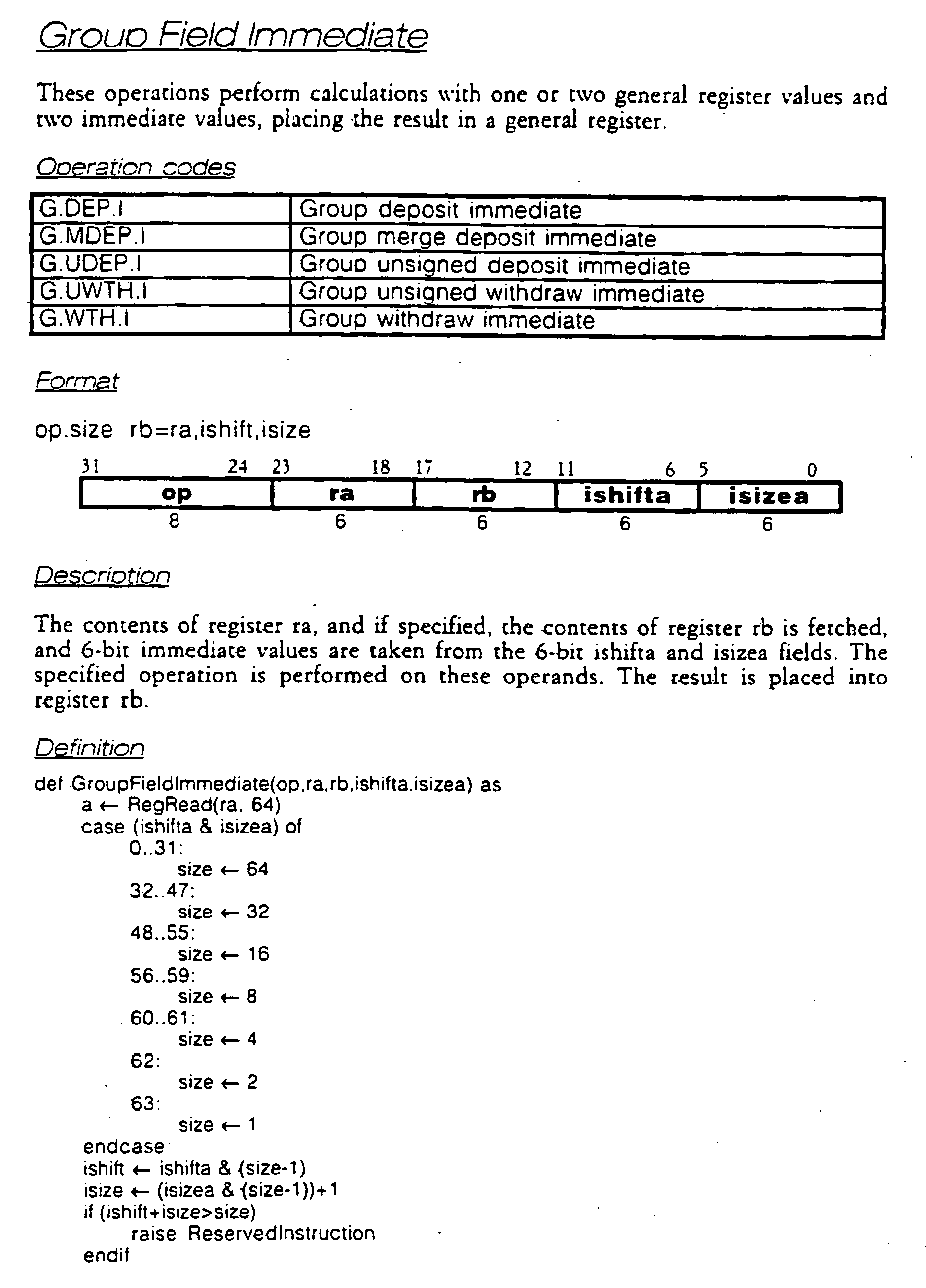


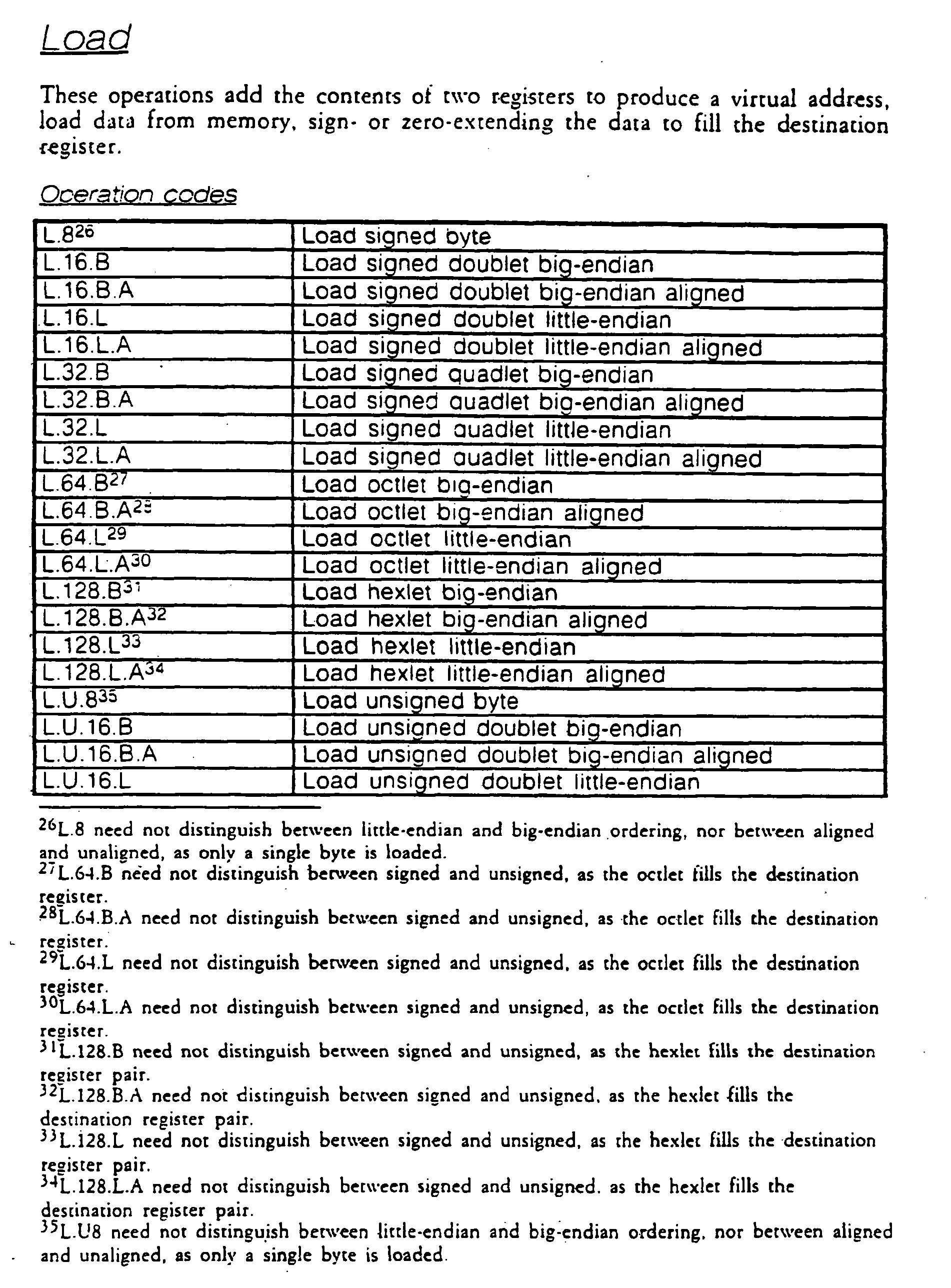


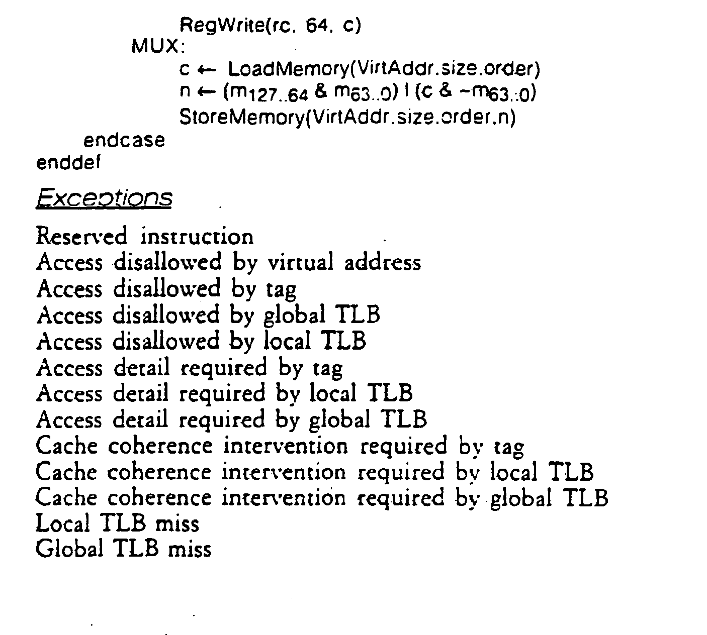


Claims (32)
- A general purpose programmable processor for processing streams of media data, the processor comprising:a plurality of registers (110) for storing data; andexecution means (100) for executing any of a set of group floating point instructions, each of which group floating point instructions specifies (i) that it is a group operation, (ii) the group floating point operation to be carried out, and (iii) the registers from which data is to be read for that operation, and wherein said execution means are configured such that the execution of a said group floating point instruction causes the execution means:i. to read data from registers specified by the group floating point instruction;ii. to partition the data read from each specified register into a respective plurality of data elements of a size in which each data element in a plurality of data elements has a corresponding data element in another plurality of data elements, thereby providing sets of corresponding data elements;iii. to carry out the floating point operation specified by the group floating point instruction on each set of corresponding data elements to produce a result for each set of corresponding data elements; andiv. to provide concatenated results to a register, wherein in response to a group floating point instruction specifying plural floating point operations on data elements representing floating point operands floating point exceptions may occur in said floating point operations of said group floating point instruction, and wherein said floating point instruction specifies whether in the event of a floating point exception occurring in a floating point operation of said group floating point instruction, an exception is raised for said group floating point instruction or the exception is handled by proceeding without a trap.
- A processor according to claim 1, wherein the set of group floating point instructions comprises group floating point instructions to operate on different data element sizes.
- A processor according to claim 1 or 2, wherein the data element size is further specified by the group floating point instruction.
- A processor according to claim 1, 2 or 3, wherein the execution means (100) is operable to execute a plurality of instructions including floating point and the group floating point instructions.
- A processor according to claim 1, 2 or 3, wherein the execution means (100) is operable to execute a plurality of instructions including the group floating point instructions and multi-precision floating point instructions.
- A processor according to any preceding claim, wherein the set of group instructions further includes a group floating point multiply-and-add instruction which causes the execution means (100) to perform all of steps (i) to (v) below:i. to partition data read from first and second registers (110) into respective pluralities of data elements of a size specified by the group floating point multiply-and-add instruction;ii. to multiply corresponding data elements from the first and second registers to produce a corresponding set of products;iii. to partition data read from a third register into a plurality of data elements of a size specified by the group floating point instruction;iv. to add to each of the set of products a respective corresponding data element from the third register to produce results; andv. to provide concatenated results to a register.
- A processor according to any preceding claim, wherein the set of group floating point instructions includes a group floating point multiply-and-subtract instruction which causes the execution means (100) to perform all of steps (i) to (v) below:i. to partition data read from first and second registers (110) into respective pluralities of data elements of a size specified by the group floating point multiply-and-subtract instruction;ii. to multiply corresponding data elements from the first and second registers to produce a corresponding set of products;iii. to partition data read from a third register into a plurality of data elements of a size specified by the group floating point instruction;iv. to subtract from each of the set of products a respective corresponding data element from the third register to produce results; andv. to provide the concatenated results to a register.
- A processor according to any of the preceding claims, wherein the set of group floating point instructions further includes a group floating point add instruction.
- A processor according to any of the preceding claims, wherein the set of group floating point instructions further includes a group floating point subtract instruction.
- A processor according to any of the preceding claims, wherein the set of group floating point instructions further includes a group floating point multiply instruction.
- A processor according to any of the preceding claims, wherein the execution means is capable of executing 16-bit group floating point instructions.
- A processor according to any of the preceding claims, wherein the execution means is capable of executing 32-bit group floating point instructions.
- A processor according to any of the preceding claims, wherein the execution means is capable of executing 64-bit group floating point instructions.
- A processor according to any of the preceding claims, wherein the set of group floating point instructions includes a group floating point divide instruction.
- A processor according to any preceding claim, wherein the execution means (100) is further capable of executing a group floating point negate instruction which causes the execution means to partition data read from a said register (110) into a first plurality of floating point data elements, to apply a negation function to each data element in the register to produce a plurality of negated data elements and to provide the plurality of negated data elements as concatenated results to a destination register.
- A processor according to any preceding claim, wherein the execution means (100) is further capable of executing a group floating point absolute instruction which causes the execution means (i) to partition data read from a register (110) into a first plurality of floating point data elements, (ii) to apply an absolute value function to each data element to produce a plurality of absolute-valued data elements and (iii) to provide the plurality of absolute-valued data elements as concatenated results to a destination register.
- A processor according to any preceding claim, wherein the execution means (100) is further capable of executing scalar arithmetic add and subtract instructions which cause the execution means:i. to partition data read from first and second registers (110) into respective pluralities of data elements;ii. to add a first operand from the first register (110) to a second operand from the second register (110) to produce an addition result and to provide the addition result to a destination register, in response to a said scalar arithmetic add instruction; andiii. to subtract a first operand from the first register from a second operand from the second register to produce a subtraction result and to provide the subtraction result to a destination register, in response to a said scalar arithmetic subtract instruction.
- A processor according to any preceding claim, wherein the execution means (100) is further capable of executing an instruction on an operand contained in a said register (110) to produce a value indicative of the most significant bit and to provide the result to a destination register (110).
- A processor according to claim 18, wherein the result represents the number of bits following the most significant bit.
- A processor according to any preceding claim, wherein the execution means (100) is further capable of carrying out a select instruction which causes the execution means (i) to partition data read from a said register (110) into a respective plurality of data elements;ii) to select one of said plurality of data elements on the basis of each of a plurality of indices; andiii) to provide the data element selected by each index to a predetermined position in concatenated results, in response to a said select instruction.
- A processor according to any preceding claim, wherein the execution means (100) is further capable of executing a reverse instruction which causes the execution means:i) to partition data read from a said register (110) into a plurality of data elements; andii) to reverse the order of data elements within said register.
- A processor according to any preceding claim, wherein the execution means (100) is further capable of executing a duplication instruction which causes the execution means:i) to partition data read from a said register into a plurality of data elements; andii) to duplicate a scalar value specified in the register, into every data element of concatenated results which are returned to a destination register.
- A processor according to any preceding claim, wherein the execution means (100) is further capable of executing a group shift left immediate instruction specifying a shift amount as an immediate value which causes the execution means:i. to partition data read from a said register into a first plurality of data elements;ii. to shift a subfield of each of the first plurality of data elements of the register towards the most significant bit by the shift amount specified by the group shift left immediate instruction to produce a second plurality of data elements twice as wide as the first plurality of data elements and to provide the second plurality of data elements as concatenated results to a destination register.
- A processor according to any preceding claim, wherein the execution means (100) is further capable of executing a group shift left instruction specifying a register containing a shift amount which causes the execution means:i. to partition data read from a said register into a first plurality of data elements;ii. to shift a subfield of each of the first plurality of data elements of the register towards the most significant bit by the shift amount to produce a second plurality of data elements and to provide the second plurality of data elements as concatenated results to a destination register.
- A processor according to any preceding claim, wherein the execution means (100) is further capable of executing a group shift right immediate instruction specifying a shift amount as an immediate value which causes the execution means:i. to partition data read from a said register into a first plurality of data elements;ii. to shift a subfield of each of the first plurality of data elements of the register towards the least significant bit by the shift amount specified by the group shift right immediate instruction to produce a second plurality of data elements half as wide as the first plurality of data elements and to provide the second plurality of data elements as concatenated results to a destination register.
- A processor according to any preceding claim, wherein the execution means (100) is further capable of executing a group shift right instruction specifying a register containing a shift amount which causes the execution means:i. to partition data read from a said register into a first plurality of data elements;ii. to shift a subfield of each of the first plurality of data elements of the register towards the least significant bit by the shift amount to produce a second plurality of data elements, and to provide the second plurality of data elements as concatenated results to a destination register.
- A processor according to any of claims 1 to 22, wherein the execution means (100) is further capable of executing a group shift instruction specifying a shift amount as an immediate value which causes the execution means:i. to partition data read from a said register into a plurality of data elements;ii. to shift a subfield of each of the plurality of data elements of the register by the shift amount to produce a plurality of shifted values and to insert each of the shifted values into a subfield within one of a second plurality of data elements in a destination register.
- A processor according to any preceding claim, wherein the execution means (100) is capable of executing an interleave instruction which causes the execution means:i. to partition data read from a first register into a first plurality of data elements and to partition data read from a second register into a second plurality of data elements;ii. to interleave the first plurality of data elements from the first register with the second plurality of data elements from the second register, and to provide concatenated results to a destination register.
- A processor according to any preceding claim, wherein the execution means (100) is further capable of executing a de-interleave instruction which causes the execution means:i. to partition data read from a first register into a first plurality of data elements and to partition data read from a second register into a second plurality of data elements;ii. to de-interleave the first plurality of data elements from the first register and the second plurality of data elements from the second register by combining select elements from the first plurality of data elements with select elements from the second plurality of data elements, and to provide concatenated results to a destination register.
- A processor according to any of the preceding claims, wherein the execution means (100) is capable of executing at least one group instruction specifying an operation to partition data from first and second registers into data elements and to add corresponding data elements from the first and second registers, at least one group instruction specifying an operation to partition data from first and second registers into data elements and to subtract corresponding data elements from the first and second registers, at least one group instruction specifying an operation to partition data from first and second registers into data elements and to multiply corresponding data elements from the first and second registers s, and at least one group instruction specifying an operation to partition data from first and second registers into data elements and to divide a data element from the first register by the corresponding data element from the second register.
- A processor according to any of the preceding claims, wherein the registers are 64-bit general purpose registers or pairs of 64-bit general purpose registers.
- A processor according to any of the preceding claims, wherein the different types of media data comprise audio and video data.
Applications Claiming Priority (2)
| Application Number | Priority Date | Filing Date | Title |
|---|---|---|---|
| US08/516,036 US5742840A (en) | 1995-08-16 | 1995-08-16 | General purpose, multiple precision parallel operation, programmable media processor |
| EP96928129A EP0845120B1 (en) | 1995-08-16 | 1996-08-16 | General purpose, programmable media processor |
Related Parent Applications (2)
| Application Number | Title | Priority Date | Filing Date |
|---|---|---|---|
| EP96928129A Division EP0845120B1 (en) | 1995-08-16 | 1996-08-16 | General purpose, programmable media processor |
| EP96928129.4 Division | 1997-02-27 |
Publications (4)
| Publication Number | Publication Date |
|---|---|
| EP1876524A2 EP1876524A2 (en) | 2008-01-09 |
| EP1876524A3 EP1876524A3 (en) | 2008-03-19 |
| EP1876524B1 true EP1876524B1 (en) | 2011-10-12 |
| EP1876524B8 EP1876524B8 (en) | 2012-03-14 |
Family
ID=24053859
Family Applications (14)
| Application Number | Title | Priority Date | Filing Date |
|---|---|---|---|
| EP07112548A Expired - Lifetime EP1879398B1 (en) | 1995-08-16 | 1996-08-16 | Set top box for processing media data |
| EP07111476A Withdrawn EP1876536A3 (en) | 1995-08-16 | 1996-08-16 | General purpose, programmable media processor |
| EP07111473A Withdrawn EP1876535A3 (en) | 1995-08-16 | 1996-08-16 | General purpose, programmable media processor |
| EP07111480A Withdrawn EP1879397A3 (en) | 1995-08-16 | 1996-08-16 | General purpose, programmable media processor |
| EP07111349A Withdrawn EP1873653A3 (en) | 1995-08-16 | 1996-08-16 | General purpose, programmable media processor |
| EP07111351A Expired - Lifetime EP1876524B8 (en) | 1995-08-16 | 1996-08-16 | General purpose, programmable media processor executing groups floating point instructions |
| EP07111350A Withdrawn EP1873654A3 (en) | 1995-08-16 | 1996-08-16 | General purpose, programmable media processor |
| EP07111352A Expired - Lifetime EP1873630B8 (en) | 1995-08-16 | 1996-08-16 | General purpose, programmable media processor |
| EP07111348A Withdrawn EP1873629A3 (en) | 1995-08-16 | 1996-08-16 | General purpose, programmable media processor |
| EP07112553A Withdrawn EP1879104A3 (en) | 1995-08-16 | 1996-08-16 | General purpose, programmable media processor |
| EP07112538A Expired - Lifetime EP1879102B1 (en) | 1995-08-16 | 1996-08-16 | General purpose, programmable media processor |
| EP96928129A Expired - Lifetime EP0845120B1 (en) | 1995-08-16 | 1996-08-16 | General purpose, programmable media processor |
| EP07111344A Withdrawn EP1873628A3 (en) | 1995-08-16 | 1996-08-16 | General purpose, programmable media processor |
| EP07112545A Expired - Lifetime EP1879103B1 (en) | 1995-08-16 | 1996-08-16 | Wireless device including a general purpose, programmable processor |
Family Applications Before (5)
| Application Number | Title | Priority Date | Filing Date |
|---|---|---|---|
| EP07112548A Expired - Lifetime EP1879398B1 (en) | 1995-08-16 | 1996-08-16 | Set top box for processing media data |
| EP07111476A Withdrawn EP1876536A3 (en) | 1995-08-16 | 1996-08-16 | General purpose, programmable media processor |
| EP07111473A Withdrawn EP1876535A3 (en) | 1995-08-16 | 1996-08-16 | General purpose, programmable media processor |
| EP07111480A Withdrawn EP1879397A3 (en) | 1995-08-16 | 1996-08-16 | General purpose, programmable media processor |
| EP07111349A Withdrawn EP1873653A3 (en) | 1995-08-16 | 1996-08-16 | General purpose, programmable media processor |
Family Applications After (8)
| Application Number | Title | Priority Date | Filing Date |
|---|---|---|---|
| EP07111350A Withdrawn EP1873654A3 (en) | 1995-08-16 | 1996-08-16 | General purpose, programmable media processor |
| EP07111352A Expired - Lifetime EP1873630B8 (en) | 1995-08-16 | 1996-08-16 | General purpose, programmable media processor |
| EP07111348A Withdrawn EP1873629A3 (en) | 1995-08-16 | 1996-08-16 | General purpose, programmable media processor |
| EP07112553A Withdrawn EP1879104A3 (en) | 1995-08-16 | 1996-08-16 | General purpose, programmable media processor |
| EP07112538A Expired - Lifetime EP1879102B1 (en) | 1995-08-16 | 1996-08-16 | General purpose, programmable media processor |
| EP96928129A Expired - Lifetime EP0845120B1 (en) | 1995-08-16 | 1996-08-16 | General purpose, programmable media processor |
| EP07111344A Withdrawn EP1873628A3 (en) | 1995-08-16 | 1996-08-16 | General purpose, programmable media processor |
| EP07112545A Expired - Lifetime EP1879103B1 (en) | 1995-08-16 | 1996-08-16 | Wireless device including a general purpose, programmable processor |
Country Status (7)
| Country | Link |
|---|---|
| US (7) | US5742840A (en) |
| EP (14) | EP1879398B1 (en) |
| AT (5) | ATE484022T1 (en) |
| AU (1) | AU6771696A (en) |
| DE (2) | DE69638268D1 (en) |
| ES (1) | ES2275453T1 (en) |
| WO (1) | WO1997007450A1 (en) |
Families Citing this family (381)
| Publication number | Priority date | Publication date | Assignee | Title |
|---|---|---|---|---|
| US7380092B2 (en) * | 2002-06-28 | 2008-05-27 | Rambus Inc. | Memory device and system having a variable depth write buffer and preload method |
| US7187572B2 (en) * | 2002-06-28 | 2007-03-06 | Rambus Inc. | Early read after write operation memory device, system and method |
| US6389010B1 (en) * | 1995-10-05 | 2002-05-14 | Intermec Ip Corp. | Hierarchical data collection network supporting packetized voice communications among wireless terminals and telephones |
| US7301541B2 (en) | 1995-08-16 | 2007-11-27 | Microunity Systems Engineering, Inc. | Programmable processor and method with wide operations |
| US6295599B1 (en) * | 1995-08-16 | 2001-09-25 | Microunity Systems Engineering | System and method for providing a wide operand architecture |
| US5742840A (en) * | 1995-08-16 | 1998-04-21 | Microunity Systems Engineering, Inc. | General purpose, multiple precision parallel operation, programmable media processor |
| US6643765B1 (en) * | 1995-08-16 | 2003-11-04 | Microunity Systems Engineering, Inc. | Programmable processor with group floating point operations |
| US5953241A (en) * | 1995-08-16 | 1999-09-14 | Microunity Engeering Systems, Inc. | Multiplier array processing system with enhanced utilization at lower precision for group multiply and sum instruction |
| US6385634B1 (en) | 1995-08-31 | 2002-05-07 | Intel Corporation | Method for performing multiply-add operations on packed data |
| US7395298B2 (en) * | 1995-08-31 | 2008-07-01 | Intel Corporation | Method and apparatus for performing multiply-add operations on packed data |
| EP0767544A3 (en) | 1995-10-04 | 2002-02-27 | Interuniversitair Micro-Elektronica Centrum Vzw | Programmable modem using spread spectrum communication |
| US6101590A (en) * | 1995-10-10 | 2000-08-08 | Micro Unity Systems Engineering, Inc. | Virtual memory system with local and global virtual address translation |
| US6035369A (en) | 1995-10-19 | 2000-03-07 | Rambus Inc. | Method and apparatus for providing a memory with write enable information |
| US6810449B1 (en) | 1995-10-19 | 2004-10-26 | Rambus, Inc. | Protocol for communication with dynamic memory |
| US6470405B2 (en) * | 1995-10-19 | 2002-10-22 | Rambus Inc. | Protocol for communication with dynamic memory |
| US7099949B1 (en) * | 1995-10-23 | 2006-08-29 | Imec Vzw | Interprocess communication protocol system |
| US6212566B1 (en) * | 1996-01-26 | 2001-04-03 | Imec | Interprocess communication protocol system modem |
| US6792523B1 (en) * | 1995-12-19 | 2004-09-14 | Intel Corporation | Processor with instructions that operate on different data types stored in the same single logical register file |
| US5940859A (en) * | 1995-12-19 | 1999-08-17 | Intel Corporation | Emptying packed data state during execution of packed data instructions |
| US8280334B2 (en) | 1996-02-05 | 2012-10-02 | American Radio Llc | System and method for radio signal reconstruction using signal processor |
| US5864754A (en) * | 1996-02-05 | 1999-01-26 | Hotto; Robert | System and method for radio signal reconstruction using signal processor |
| US7099316B1 (en) * | 1996-02-29 | 2006-08-29 | Tomich John L | Photonic home area network |
| US6209071B1 (en) | 1996-05-07 | 2001-03-27 | Rambus Inc. | Asynchronous request/synchronous data dynamic random access memory |
| JPH1049356A (en) * | 1996-07-31 | 1998-02-20 | Matsushita Electric Ind Co Ltd | Media flow control system |
| JP3560423B2 (en) * | 1996-09-17 | 2004-09-02 | 松下電器産業株式会社 | Packet transmitting / receiving device and packet receiving device |
| US6473404B1 (en) * | 1998-11-24 | 2002-10-29 | Connect One, Inc. | Multi-protocol telecommunications routing optimization |
| US6016307A (en) | 1996-10-31 | 2000-01-18 | Connect One, Inc. | Multi-protocol telecommunications routing optimization |
| US6230245B1 (en) | 1997-02-11 | 2001-05-08 | Micron Technology, Inc. | Method and apparatus for generating a variable sequence of memory device command signals |
| US6175894B1 (en) | 1997-03-05 | 2001-01-16 | Micron Technology, Inc. | Memory device command buffer apparatus and method and memory devices and computer systems using same |
| US6359882B1 (en) | 1997-04-01 | 2002-03-19 | Yipes Communications, Inc. | Method and apparatus for transmitting data |
| US6101255A (en) * | 1997-04-30 | 2000-08-08 | Motorola, Inc. | Programmable cryptographic processing system and method |
| US6611537B1 (en) * | 1997-05-30 | 2003-08-26 | Centillium Communications, Inc. | Synchronous network for digital media streams |
| US5996043A (en) | 1997-06-13 | 1999-11-30 | Micron Technology, Inc. | Two step memory device command buffer apparatus and method and memory devices and computer systems using same |
| US6484244B1 (en) | 1997-06-17 | 2002-11-19 | Micron Technology, Inc. | Method and system for storing and processing multiple memory commands |
| US6266379B1 (en) | 1997-06-20 | 2001-07-24 | Massachusetts Institute Of Technology | Digital transmitter with equalization |
| US6009264A (en) * | 1997-08-28 | 1999-12-28 | Ncr Corporation | Node coordination using a channel object and point-to-point protocol |
| US6870419B1 (en) | 1997-08-29 | 2005-03-22 | Rambus Inc. | Memory system including a memory device having a controlled output driver characteristic |
| US6067594A (en) * | 1997-09-26 | 2000-05-23 | Rambus, Inc. | High frequency bus system |
| US7197625B1 (en) | 1997-10-09 | 2007-03-27 | Mips Technologies, Inc. | Alignment and ordering of vector elements for single instruction multiple data processing |
| US5864703A (en) | 1997-10-09 | 1999-01-26 | Mips Technologies, Inc. | Method for providing extended precision in SIMD vector arithmetic operations |
| US6401167B1 (en) * | 1997-10-10 | 2002-06-04 | Rambus Incorporated | High performance cost optimized memory |
| US6343352B1 (en) | 1997-10-10 | 2002-01-29 | Rambus Inc. | Method and apparatus for two step memory write operations |
| WO1999019875A2 (en) * | 1997-10-10 | 1999-04-22 | Rambus Incorporated | Apparatus and method for pipelined memory operations |
| US7167927B2 (en) | 1997-10-14 | 2007-01-23 | Alacritech, Inc. | TCP/IP offload device with fast-path TCP ACK generating and transmitting mechanism |
| US6697868B2 (en) | 2000-02-28 | 2004-02-24 | Alacritech, Inc. | Protocol processing stack for use with intelligent network interface device |
| US7133940B2 (en) * | 1997-10-14 | 2006-11-07 | Alacritech, Inc. | Network interface device employing a DMA command queue |
| US6226680B1 (en) * | 1997-10-14 | 2001-05-01 | Alacritech, Inc. | Intelligent network interface system method for protocol processing |
| US6658480B2 (en) | 1997-10-14 | 2003-12-02 | Alacritech, Inc. | Intelligent network interface system and method for accelerated protocol processing |
| US6687758B2 (en) * | 2001-03-07 | 2004-02-03 | Alacritech, Inc. | Port aggregation for network connections that are offloaded to network interface devices |
| US6389479B1 (en) | 1997-10-14 | 2002-05-14 | Alacritech, Inc. | Intelligent network interface device and system for accelerated communication |
| US6757746B2 (en) | 1997-10-14 | 2004-06-29 | Alacritech, Inc. | Obtaining a destination address so that a network interface device can write network data without headers directly into host memory |
| US8782199B2 (en) | 1997-10-14 | 2014-07-15 | A-Tech Llc | Parsing a packet header |
| US7174393B2 (en) | 2000-12-26 | 2007-02-06 | Alacritech, Inc. | TCP/IP offload network interface device |
| US7042898B2 (en) | 1997-10-14 | 2006-05-09 | Alacritech, Inc. | Reducing delays associated with inserting a checksum into a network message |
| US6427171B1 (en) | 1997-10-14 | 2002-07-30 | Alacritech, Inc. | Protocol processing stack for use with intelligent network interface device |
| US7284070B2 (en) * | 1997-10-14 | 2007-10-16 | Alacritech, Inc. | TCP offload network interface device |
| US6591302B2 (en) | 1997-10-14 | 2003-07-08 | Alacritech, Inc. | Fast-path apparatus for receiving data corresponding to a TCP connection |
| US7185266B2 (en) | 2003-02-12 | 2007-02-27 | Alacritech, Inc. | Network interface device for error detection using partial CRCS of variable length message portions |
| US7237036B2 (en) | 1997-10-14 | 2007-06-26 | Alacritech, Inc. | Fast-path apparatus for receiving data corresponding a TCP connection |
| US6434620B1 (en) | 1998-08-27 | 2002-08-13 | Alacritech, Inc. | TCP/IP offload network interface device |
| US7089326B2 (en) * | 1997-10-14 | 2006-08-08 | Alacritech, Inc. | Fast-path processing for receiving data on TCP connection offload devices |
| US6470415B1 (en) | 1999-10-13 | 2002-10-22 | Alacritech, Inc. | Queue system involving SRAM head, SRAM tail and DRAM body |
| US7076568B2 (en) * | 1997-10-14 | 2006-07-11 | Alacritech, Inc. | Data communication apparatus for computer intelligent network interface card which transfers data between a network and a storage device according designated uniform datagram protocol socket |
| US6353927B1 (en) * | 1997-10-14 | 2002-03-05 | Lucent Technologies Inc. | Data download technique into installed memory |
| US8539112B2 (en) | 1997-10-14 | 2013-09-17 | Alacritech, Inc. | TCP/IP offload device |
| US6807581B1 (en) | 2000-09-29 | 2004-10-19 | Alacritech, Inc. | Intelligent network storage interface system |
| US6427173B1 (en) | 1997-10-14 | 2002-07-30 | Alacritech, Inc. | Intelligent network interfaced device and system for accelerated communication |
| US8621101B1 (en) | 2000-09-29 | 2013-12-31 | Alacritech, Inc. | Intelligent network storage interface device |
| US6202119B1 (en) * | 1997-12-19 | 2001-03-13 | Micron Technology, Inc. | Method and system for processing pipelined memory commands |
| US6279045B1 (en) * | 1997-12-29 | 2001-08-21 | Kawasaki Steel Corporation | Multimedia interface having a multimedia processor and a field programmable gate array |
| US6041404A (en) | 1998-03-31 | 2000-03-21 | Intel Corporation | Dual function system and method for shuffling packed data elements |
| US7392275B2 (en) * | 1998-03-31 | 2008-06-24 | Intel Corporation | Method and apparatus for performing efficient transformations with horizontal addition and subtraction |
| US6230253B1 (en) * | 1998-03-31 | 2001-05-08 | Intel Corporation | Executing partial-width packed data instructions |
| US6230257B1 (en) * | 1998-03-31 | 2001-05-08 | Intel Corporation | Method and apparatus for staggering execution of a single packed data instruction using the same circuit |
| US6625638B1 (en) * | 1998-04-30 | 2003-09-23 | International Business Machines Corporation | Management of a logical partition that supports different types of processors |
| US7100020B1 (en) * | 1998-05-08 | 2006-08-29 | Freescale Semiconductor, Inc. | Digital communications processor |
| FR2778762B1 (en) * | 1998-05-14 | 2000-12-08 | Sgs Thomson Microelectronics | MICROPROCESSOR INTERFACE WITH AN EXTERNAL MEMORY OPTIMIZED BY AN EARLY DECODING SYSTEM |
| US6480876B2 (en) * | 1998-05-28 | 2002-11-12 | Compaq Information Technologies Group, L.P. | System for integrating task and data parallelism in dynamic applications |
| US6675189B2 (en) * | 1998-05-28 | 2004-01-06 | Hewlett-Packard Development Company, L.P. | System for learning and applying integrated task and data parallel strategies in dynamic applications |
| US6650327B1 (en) | 1998-06-16 | 2003-11-18 | Silicon Graphics, Inc. | Display system having floating point rasterization and floating point framebuffering |
| US6175905B1 (en) | 1998-07-30 | 2001-01-16 | Micron Technology, Inc. | Method and system for bypassing pipelines in a pipelined memory command generator |
| EP1046100A1 (en) * | 1998-08-06 | 2000-10-25 | Trimedia Technologies, Inc. | Data processor and method of processing data |
| US7932911B2 (en) | 1998-08-24 | 2011-04-26 | Microunity Systems Engineering, Inc. | Processor for executing switch and translate instructions requiring wide operands |
| US6378060B1 (en) | 1998-08-24 | 2002-04-23 | Microunity Systems Engineering, Inc. | System to implement a cross-bar switch of a broadband processor |
| EP1105792B1 (en) * | 1998-08-24 | 2010-05-05 | MicroUnity Systems Engineering, Inc. | System with wide operand architecture, and method |
| ATE467171T1 (en) * | 1998-08-24 | 2010-05-15 | Microunity Systems Eng | SYSTEM WITH WIDE OPERANDE ARCHITECTURE AND PROCEDURES |
| US6178488B1 (en) | 1998-08-27 | 2001-01-23 | Micron Technology, Inc. | Method and apparatus for processing pipelined memory commands |
| US7664883B2 (en) | 1998-08-28 | 2010-02-16 | Alacritech, Inc. | Network interface device that fast-path processes solicited session layer read commands |
| US6418518B1 (en) * | 1998-09-18 | 2002-07-09 | National Semiconductor Corporation | Decoupled address and data access to an SDRAM |
| JP3164083B2 (en) * | 1998-10-20 | 2001-05-08 | 日本電気株式会社 | Semiconductor integrated circuit |
| US6041400A (en) * | 1998-10-26 | 2000-03-21 | Sony Corporation | Distributed extensible processing architecture for digital signal processing applications |
| JP3374967B2 (en) * | 1998-10-26 | 2003-02-10 | 日本電気株式会社 | Semiconductor integrated circuit |
| US6747984B1 (en) | 1998-12-18 | 2004-06-08 | Lsi Logic Corporation | Method and apparatus for transmitting Data |
| WO2000048070A1 (en) * | 1999-02-12 | 2000-08-17 | Microunity Systems Engineering, Inc. | System and method to implement a cross-bar switch of a broadband processor |
| DE69902221T2 (en) * | 1999-02-23 | 2003-03-06 | Taiwan Semiconductor Mfg | Memory circuits with built-in self-test |
| US7243133B2 (en) * | 1999-03-30 | 2007-07-10 | Sedna Patent Services, Llc | Method and apparatus for reducing latency in an interactive information distribution system |
| EP1046998A1 (en) * | 1999-04-22 | 2000-10-25 | Texas Instruments Incorporated | Digital signal processors with virtual addressing |
| US7185081B1 (en) | 1999-04-30 | 2007-02-27 | Pmc-Sierra, Inc. | Method and apparatus for programmable lexical packet classifier |
| US7188168B1 (en) | 1999-04-30 | 2007-03-06 | Pmc-Sierra, Inc. | Method and apparatus for grammatical packet classifier |
| EP1059781B1 (en) * | 1999-05-06 | 2007-09-05 | Siemens Aktiengesellschaft | Communication device with real-time transmission data processing means |
| US6463548B1 (en) * | 1999-05-10 | 2002-10-08 | Compaq Information Technologies Group, L.P. | Method and apparatus to enforce clocked circuit functionality at reduced frequency without limiting peak performance |
| US6718415B1 (en) | 1999-05-14 | 2004-04-06 | Acqis Technology, Inc. | Computer system and method including console housing multiple computer modules having independent processing units, mass storage devices, and graphics controllers |
| US6643777B1 (en) * | 1999-05-14 | 2003-11-04 | Acquis Technology, Inc. | Data security method and device for computer modules |
| US6853651B1 (en) | 1999-06-17 | 2005-02-08 | Cingular Wireless Ii, Inc. | System and method for outbox-capable wireless transmission |
| US6598166B1 (en) * | 1999-08-18 | 2003-07-22 | Sun Microsystems, Inc. | Microprocessor in which logic changes during execution |
| US6460120B1 (en) * | 1999-08-27 | 2002-10-01 | International Business Machines Corporation | Network processor, memory organization and methods |
| US20020071321A1 (en) * | 2000-11-29 | 2002-06-13 | International Business Machines Corporation | System and method of maintaining high bandwidth requirement of a data pipe from low bandwidth memories |
| US7051130B1 (en) | 1999-10-19 | 2006-05-23 | Rambus Inc. | Integrated circuit device that stores a value representative of a drive strength setting |
| US6643787B1 (en) | 1999-10-19 | 2003-11-04 | Rambus Inc. | Bus system optimization |
| US6321282B1 (en) | 1999-10-19 | 2001-11-20 | Rambus Inc. | Apparatus and method for topography dependent signaling |
| US6646953B1 (en) * | 2000-07-06 | 2003-11-11 | Rambus Inc. | Single-clock, strobeless signaling system |
| US6643752B1 (en) * | 1999-12-09 | 2003-11-04 | Rambus Inc. | Transceiver with latency alignment circuitry |
| US7793076B1 (en) * | 1999-12-17 | 2010-09-07 | Intel Corporation | Digital signals processor having a plurality of independent dedicated processors |
| US6847365B1 (en) * | 2000-01-03 | 2005-01-25 | Genesis Microchip Inc. | Systems and methods for efficient processing of multimedia data |
| US7404032B2 (en) * | 2000-01-05 | 2008-07-22 | Rambus Inc. | Configurable width buffered module having switch elements |
| US7356639B2 (en) * | 2000-01-05 | 2008-04-08 | Rambus Inc. | Configurable width buffered module having a bypass circuit |
| US7363422B2 (en) * | 2000-01-05 | 2008-04-22 | Rambus Inc. | Configurable width buffered module |
| US7266634B2 (en) * | 2000-01-05 | 2007-09-04 | Rambus Inc. | Configurable width buffered module having flyby elements |
| US20050010737A1 (en) * | 2000-01-05 | 2005-01-13 | Fred Ware | Configurable width buffered module having splitter elements |
| US7017002B2 (en) * | 2000-01-05 | 2006-03-21 | Rambus, Inc. | System featuring a master device, a buffer device and a plurality of integrated circuit memory devices |
| US6502161B1 (en) * | 2000-01-05 | 2002-12-31 | Rambus Inc. | Memory system including a point-to-point linked memory subsystem |
| US20010028662A1 (en) * | 2000-01-18 | 2001-10-11 | Hunt Paul M. | Method and system of real-time optimization and implementation of content and advertising programming decisions for broadcasts and narrowcasts |
| US7502876B1 (en) | 2000-06-23 | 2009-03-10 | Mips Technologies, Inc. | Background memory manager that determines if data structures fits in memory with memory state transactions map |
| US7042887B2 (en) | 2000-02-08 | 2006-05-09 | Mips Technologies, Inc. | Method and apparatus for non-speculative pre-fetch operation in data packet processing |
| US7155516B2 (en) | 2000-02-08 | 2006-12-26 | Mips Technologies, Inc. | Method and apparatus for overflowing data packets to a software-controlled memory when they do not fit into a hardware-controlled memory |
| US7649901B2 (en) | 2000-02-08 | 2010-01-19 | Mips Technologies, Inc. | Method and apparatus for optimizing selection of available contexts for packet processing in multi-stream packet processing |
| US20010052053A1 (en) * | 2000-02-08 | 2001-12-13 | Mario Nemirovsky | Stream processing unit for a multi-streaming processor |
| US7058065B2 (en) * | 2000-02-08 | 2006-06-06 | Mips Tech Inc | Method and apparatus for preventing undesirable packet download with pending read/write operations in data packet processing |
| US7058064B2 (en) * | 2000-02-08 | 2006-06-06 | Mips Technologies, Inc. | Queueing system for processors in packet routing operations |
| US7165257B2 (en) * | 2000-02-08 | 2007-01-16 | Mips Technologies, Inc. | Context selection and activation mechanism for activating one of a group of inactive contexts in a processor core for servicing interrupts |
| US7032226B1 (en) * | 2000-06-30 | 2006-04-18 | Mips Technologies, Inc. | Methods and apparatus for managing a buffer of events in the background |
| US7139901B2 (en) * | 2000-02-08 | 2006-11-21 | Mips Technologies, Inc. | Extended instruction set for packet processing applications |
| US7065096B2 (en) | 2000-06-23 | 2006-06-20 | Mips Technologies, Inc. | Method for allocating memory space for limited packet head and/or tail growth |
| US7082552B2 (en) | 2000-02-08 | 2006-07-25 | Mips Tech Inc | Functional validation of a packet management unit |
| US7076630B2 (en) * | 2000-02-08 | 2006-07-11 | Mips Tech Inc | Method and apparatus for allocating and de-allocating consecutive blocks of memory in background memo management |
| CN1184575C (en) * | 2000-04-07 | 2005-01-12 | 北京华诺信息技术有限公司 | Software defined cable network system and method |
| US7024461B1 (en) * | 2000-04-28 | 2006-04-04 | Nortel Networks Limited | Session initiation protocol enabled set-top device |
| US7010788B1 (en) | 2000-05-19 | 2006-03-07 | Hewlett-Packard Development Company, L.P. | System for computing the optimal static schedule using the stored task execution costs with recent schedule execution costs |
| US6751746B1 (en) * | 2000-07-31 | 2004-06-15 | Cisco Technology, Inc. | Method and apparatus for uninterrupted packet transfer using replication over disjoint paths |
| US7287009B1 (en) * | 2000-09-14 | 2007-10-23 | Raanan Liebermann | System and a method for carrying out personal and business transactions |
| US8019901B2 (en) | 2000-09-29 | 2011-09-13 | Alacritech, Inc. | Intelligent network storage interface system |
| US6720074B2 (en) * | 2000-10-26 | 2004-04-13 | Inframat Corporation | Insulator coated magnetic nanoparticulate composites with reduced core loss and method of manufacture thereof |
| GB0028079D0 (en) * | 2000-11-17 | 2001-01-03 | Imperial College | System and method |
| US6839792B2 (en) * | 2000-12-15 | 2005-01-04 | Innovative Concepts, Inc. | Data modem |
| US6760772B2 (en) | 2000-12-15 | 2004-07-06 | Qualcomm, Inc. | Generating and implementing a communication protocol and interface for high data rate signal transfer |
| US7054949B2 (en) * | 2001-01-19 | 2006-05-30 | World Streaming Network, Inc. | System and method for streaming media |
| US9674575B2 (en) | 2001-01-19 | 2017-06-06 | SITO Mobile R&D IP, LLC | System and method for routing media |
| US7191244B2 (en) * | 2001-01-19 | 2007-03-13 | Streamworks Technologies, Inc. | System and method for routing media |
| US20040025186A1 (en) * | 2001-01-19 | 2004-02-05 | Jennings Charles A. | System and method for managing media |
| US7155601B2 (en) | 2001-02-14 | 2006-12-26 | Intel Corporation | Multi-element operand sub-portion shuffle instruction execution |
| US7711763B2 (en) | 2001-02-21 | 2010-05-04 | Mips Technologies, Inc. | Microprocessor instructions for performing polynomial arithmetic operations |
| US7162621B2 (en) | 2001-02-21 | 2007-01-09 | Mips Technologies, Inc. | Virtual instruction expansion based on template and parameter selector information specifying sign-extension or concentration |
| US7123307B1 (en) * | 2001-02-23 | 2006-10-17 | Silicon Image, Inc. | Clock jitter limiting scheme in video transmission through multiple stages |
| US6877079B2 (en) * | 2001-03-06 | 2005-04-05 | Samsung Electronics Co., Ltd. | Memory system having point-to-point bus configuration |
| US6675272B2 (en) | 2001-04-24 | 2004-01-06 | Rambus Inc. | Method and apparatus for coordinating memory operations among diversely-located memory components |
| US8391039B2 (en) | 2001-04-24 | 2013-03-05 | Rambus Inc. | Memory module with termination component |
| US20020194340A1 (en) * | 2001-06-16 | 2002-12-19 | Ebstyne Bryan D. | Enterprise storage resource management system |
| US6891845B2 (en) * | 2001-06-29 | 2005-05-10 | Intel Corporation | Method and apparatus for adapting to a clock rate transition in a communications network using idles |
| US8576527B2 (en) | 2001-07-06 | 2013-11-05 | Schweitzer Engineering Laboratoris Inc | Apparatus, system, and method for creating one or more slow-speed communications channels utilizing a real-time communication channel |
| US8111492B2 (en) * | 2001-07-06 | 2012-02-07 | Schweitzer Engineering Laboratories, Inc. | Apparatus, system, and method for creating one or more slow-speed communications channels utilizing a real-time communication channel |
| US7543067B2 (en) * | 2001-08-01 | 2009-06-02 | Canon Kabushiki Kaisha | Flexible secure network data transfer and messaging |
| US8812706B1 (en) | 2001-09-06 | 2014-08-19 | Qualcomm Incorporated | Method and apparatus for compensating for mismatched delays in signals of a mobile display interface (MDDI) system |
| US20030065803A1 (en) * | 2001-09-28 | 2003-04-03 | Koninklijke Philips Electronics N. V. | Intelligent delivery method for streamed content |
| US7032215B2 (en) * | 2001-10-11 | 2006-04-18 | Intel Corporation | Method and system for type demotion of expressions and variables by bitwise constant propagation |
| US7430578B2 (en) * | 2001-10-29 | 2008-09-30 | Intel Corporation | Method and apparatus for performing multiply-add operations on packed byte data |
| US7154533B2 (en) * | 2001-10-30 | 2006-12-26 | Tandberg Telecom As | System and method for monitoring and diagnosis of video network performance |
| US7009978B2 (en) | 2001-12-18 | 2006-03-07 | Nortel Networks Limited | Communications interface for providing a plurality of communication channels to a single port on a processor |
| US20030121835A1 (en) * | 2001-12-31 | 2003-07-03 | Peter Quartararo | Apparatus for and method of sieving biocompatible adsorbent beaded polymers |
| US7260217B1 (en) * | 2002-03-01 | 2007-08-21 | Cavium Networks, Inc. | Speculative execution for data ciphering operations |
| US6839709B2 (en) * | 2002-03-19 | 2005-01-04 | Intel Corporation | Layered resource structure and method |
| US7543087B2 (en) | 2002-04-22 | 2009-06-02 | Alacritech, Inc. | Freeing transmit memory on a network interface device prior to receiving an acknowledgement that transmit data has been received by a remote device |
| US7496689B2 (en) | 2002-04-22 | 2009-02-24 | Alacritech, Inc. | TCP/IP offload device |
| US7124163B2 (en) | 2002-05-24 | 2006-10-17 | Convedia Corporation | Data server |
| US7047383B2 (en) | 2002-07-11 | 2006-05-16 | Intel Corporation | Byte swap operation for a 64 bit operand |
| CN1692343A (en) * | 2002-07-22 | 2005-11-02 | 株式会社瑞萨科技 | Semiconductor integrated circuit device, data processing system and memory system |
| JP4085255B2 (en) * | 2002-09-26 | 2008-05-14 | 富士フイルム株式会社 | Digital camera and image communication method |
| US7191241B2 (en) * | 2002-09-27 | 2007-03-13 | Alacritech, Inc. | Fast-path apparatus for receiving data corresponding to a TCP connection |
| US7337241B2 (en) * | 2002-09-27 | 2008-02-26 | Alacritech, Inc. | Fast-path apparatus for receiving data corresponding to a TCP connection |
| US9088474B2 (en) * | 2002-10-08 | 2015-07-21 | Broadcom Corporation | Advanced processor with interfacing messaging network to a CPU |
| US7334086B2 (en) * | 2002-10-08 | 2008-02-19 | Rmi Corporation | Advanced processor with system on a chip interconnect technology |
| US6842848B2 (en) * | 2002-10-11 | 2005-01-11 | Sandbridge Technologies, Inc. | Method and apparatus for token triggered multithreading |
| US20040088262A1 (en) * | 2002-11-06 | 2004-05-06 | Alacritech, Inc. | Enabling an enhanced function of an electronic device |
| US7362697B2 (en) * | 2003-01-09 | 2008-04-22 | International Business Machines Corporation | Self-healing chip-to-chip interface |
| AU2003303908A1 (en) * | 2003-02-12 | 2004-09-06 | Research In Motion Limited | An apparatus and methods for managing data used by a mobile device |
| US7290192B2 (en) * | 2003-03-31 | 2007-10-30 | Advantest Corporation | Test apparatus and test method for testing plurality of devices in parallel |
| US7119549B2 (en) * | 2003-02-25 | 2006-10-10 | Rambus Inc. | Output calibrator with dynamic precision |
| US7400586B2 (en) * | 2003-02-25 | 2008-07-15 | Avaya Technology Corp. | Collaborative remote communication circuit diagnostic tool |
| US7324555B1 (en) | 2003-03-20 | 2008-01-29 | Infovalue Computing, Inc. | Streaming while fetching broadband video objects using heterogeneous and dynamic optimized segmentation size |
| US6922770B2 (en) * | 2003-05-27 | 2005-07-26 | Sony Corporation | Memory controller providing dynamic arbitration of memory commands |
| BRPI0410885B1 (en) | 2003-06-02 | 2018-01-30 | Qualcomm Incorporated | GENERATE AND IMPLEMENT A SIGNAL AND INTERFACE PROTOCOL FOR HIGHER DATA RATES |
| US7194581B2 (en) * | 2003-06-03 | 2007-03-20 | Intel Corporation | Memory channel with hot add/remove |
| US7200787B2 (en) * | 2003-06-03 | 2007-04-03 | Intel Corporation | Memory channel utilizing permuting status patterns |
| US7127629B2 (en) * | 2003-06-03 | 2006-10-24 | Intel Corporation | Redriving a data signal responsive to either a sampling clock signal or stable clock signal dependent on a mode signal |
| US7340537B2 (en) * | 2003-06-04 | 2008-03-04 | Intel Corporation | Memory channel with redundant presence detect |
| US7165153B2 (en) | 2003-06-04 | 2007-01-16 | Intel Corporation | Memory channel with unidirectional links |
| US8171331B2 (en) | 2003-06-04 | 2012-05-01 | Intel Corporation | Memory channel having deskew separate from redrive |
| US7386768B2 (en) | 2003-06-05 | 2008-06-10 | Intel Corporation | Memory channel with bit lane fail-over |
| US7047385B1 (en) * | 2003-06-16 | 2006-05-16 | Cisco Technology, Inc. | High-speed memory for use in networking systems |
| US20070169022A1 (en) * | 2003-06-18 | 2007-07-19 | Jones Anthony M | Processor having multiple instruction sources and execution modes |
| EP1645130A1 (en) * | 2003-07-04 | 2006-04-12 | Koninklijke Philips Electronics N.V. | Method of broadcasting multimedia content via a distribution network |
| US7130963B2 (en) * | 2003-07-16 | 2006-10-31 | International Business Machines Corp. | System and method for instruction memory storage and processing based on backwards branch control information |
| EP2363989B1 (en) | 2003-08-13 | 2018-09-19 | Qualcomm Incorporated | A signal interface for higher data rates |
| JP3984206B2 (en) * | 2003-09-02 | 2007-10-03 | 株式会社東芝 | Microprocessor and video / audio system |
| ES2323129T3 (en) | 2003-09-10 | 2009-07-07 | Qualcomm Incorporated | HIGH SPEED DATA INTERFACE. |
| JP2007509533A (en) | 2003-10-15 | 2007-04-12 | クゥアルコム・インコーポレイテッド | High speed data rate interface |
| CA2544030A1 (en) * | 2003-10-29 | 2005-05-12 | Qualcomm Incorporated | High data rate interface |
| EP2242231A1 (en) | 2003-11-12 | 2010-10-20 | Qualcomm Incorporated | High data rate interface with improved link control |
| US7219294B2 (en) * | 2003-11-14 | 2007-05-15 | Intel Corporation | Early CRC delivery for partial frame |
| US7143207B2 (en) * | 2003-11-14 | 2006-11-28 | Intel Corporation | Data accumulation between data path having redrive circuit and memory device |
| US7447953B2 (en) | 2003-11-14 | 2008-11-04 | Intel Corporation | Lane testing with variable mapping |
| MXPA06006012A (en) | 2003-11-25 | 2006-08-23 | Qualcomm Inc | High data rate interface with improved link synchronization. |
| US6996070B2 (en) * | 2003-12-05 | 2006-02-07 | Alacritech, Inc. | TCP/IP offload device with reduced sequential processing |
| CA2548412C (en) | 2003-12-08 | 2011-04-19 | Qualcomm Incorporated | High data rate interface with improved link synchronization |
| WO2005066805A1 (en) * | 2003-12-26 | 2005-07-21 | Fujitsu Limited | Common memory accessing method and multiprocessor system employing it |
| EP2375676B1 (en) | 2004-03-10 | 2013-06-26 | Qualcomm Incorporated | High data rate interface apparatus and method |
| MXPA06010647A (en) | 2004-03-17 | 2007-01-17 | Qualcomm Inc | High data rate interface apparatus and method. |
| RU2006137364A (en) | 2004-03-24 | 2008-04-27 | Квэлкомм Инкорпорейтед (US) | DEVICE AND METHOD FOR HIGH-SPEED DATA TRANSFER INTERFACE |
| WO2005093654A2 (en) | 2004-03-25 | 2005-10-06 | Fatih Ozluturk | Method and apparatus to correct digital image blur due to motion of subject or imaging device |
| US7586951B2 (en) * | 2004-04-27 | 2009-09-08 | Intel Corporation | Method, apparatus, and system for idle state definition for power management |
| US7221613B2 (en) * | 2004-05-26 | 2007-05-22 | Freescale Semiconductor, Inc. | Memory with serial input/output terminals for address and data and method therefor |
| US7212423B2 (en) * | 2004-05-31 | 2007-05-01 | Intel Corporation | Memory agent core clock aligned to lane |
| US8650304B2 (en) | 2004-06-04 | 2014-02-11 | Qualcomm Incorporated | Determining a pre skew and post skew calibration data rate in a mobile display digital interface (MDDI) communication system |
| ATE518343T1 (en) | 2004-06-04 | 2011-08-15 | Qualcomm Inc | INTERFACE DEVICE AND METHOD FOR HIGH DATA RATES |
| US20060004953A1 (en) * | 2004-06-30 | 2006-01-05 | Vogt Pete D | Method and apparatus for increased memory bandwidth |
| US7383399B2 (en) * | 2004-06-30 | 2008-06-03 | Intel Corporation | Method and apparatus for memory compression |
| US7200693B2 (en) * | 2004-08-27 | 2007-04-03 | Micron Technology, Inc. | Memory system and method having unidirectional data buses |
| EP1794979B1 (en) | 2004-09-10 | 2017-04-12 | Cavium, Inc. | Selective replication of data structure |
| US7941585B2 (en) * | 2004-09-10 | 2011-05-10 | Cavium Networks, Inc. | Local scratchpad and data caching system |
| US7594081B2 (en) | 2004-09-10 | 2009-09-22 | Cavium Networks, Inc. | Direct access to low-latency memory |
| US7301831B2 (en) * | 2004-09-15 | 2007-11-27 | Rambus Inc. | Memory systems with variable delays for write data signals |
| US8248939B1 (en) | 2004-10-08 | 2012-08-21 | Alacritech, Inc. | Transferring control of TCP connections between hierarchy of processing mechanisms |
| US8723705B2 (en) | 2004-11-24 | 2014-05-13 | Qualcomm Incorporated | Low output skew double data rate serial encoder |
| US8539119B2 (en) | 2004-11-24 | 2013-09-17 | Qualcomm Incorporated | Methods and apparatus for exchanging messages having a digital data interface device message format |
| US8692838B2 (en) | 2004-11-24 | 2014-04-08 | Qualcomm Incorporated | Methods and systems for updating a buffer |
| US8873584B2 (en) | 2004-11-24 | 2014-10-28 | Qualcomm Incorporated | Digital data interface device |
| US8667363B2 (en) | 2004-11-24 | 2014-03-04 | Qualcomm Incorporated | Systems and methods for implementing cyclic redundancy checks |
| US8699330B2 (en) | 2004-11-24 | 2014-04-15 | Qualcomm Incorporated | Systems and methods for digital data transmission rate control |
| US7490215B2 (en) * | 2004-12-22 | 2009-02-10 | Intel Corporation | Media memory system and method for providing concurrent memory access to a plurality of processors through separate translation table information |
| US8667249B2 (en) | 2004-12-22 | 2014-03-04 | Intel Corporation | Systems and methods exchanging data between processors through concurrent shared memory |
| US8279886B2 (en) | 2004-12-30 | 2012-10-02 | Intel Corporation | Dataport and methods thereof |
| US20060179273A1 (en) * | 2005-02-09 | 2006-08-10 | Advanced Micro Devices, Inc. | Data processor adapted for efficient digital signal processing and method therefor |
| US9459960B2 (en) | 2005-06-03 | 2016-10-04 | Rambus Inc. | Controller device for use with electrically erasable programmable memory chip with error detection and retry modes of operation |
| US7831882B2 (en) | 2005-06-03 | 2010-11-09 | Rambus Inc. | Memory system with error detection and retry modes of operation |
| JP4673408B2 (en) * | 2005-06-03 | 2011-04-20 | エヌエックスピー ビー ヴィ | Data processing system and method for scheduling utilization of at least one exclusive resource |
| US7562271B2 (en) | 2005-09-26 | 2009-07-14 | Rambus Inc. | Memory system topologies including a buffer device and an integrated circuit memory device |
| US7464225B2 (en) * | 2005-09-26 | 2008-12-09 | Rambus Inc. | Memory module including a plurality of integrated circuit memory devices and a plurality of buffer devices in a matrix topology |
| US11328764B2 (en) | 2005-09-26 | 2022-05-10 | Rambus Inc. | Memory system topologies including a memory die stack |
| US7747833B2 (en) * | 2005-09-30 | 2010-06-29 | Mosaid Technologies Incorporated | Independent link and bank selection |
| WO2007036050A1 (en) * | 2005-09-30 | 2007-04-05 | Mosaid Technologies Incorporated | Memory with output control |
| US20070076502A1 (en) | 2005-09-30 | 2007-04-05 | Pyeon Hong B | Daisy chain cascading devices |
| US11948629B2 (en) | 2005-09-30 | 2024-04-02 | Mosaid Technologies Incorporated | Non-volatile memory device with concurrent bank operations |
| US7652922B2 (en) | 2005-09-30 | 2010-01-26 | Mosaid Technologies Incorporated | Multiple independent serial link memory |
| US8730069B2 (en) | 2005-11-23 | 2014-05-20 | Qualcomm Incorporated | Double data rate serial encoder |
| US8692839B2 (en) | 2005-11-23 | 2014-04-08 | Qualcomm Incorporated | Methods and systems for updating a buffer |
| US7738500B1 (en) | 2005-12-14 | 2010-06-15 | Alacritech, Inc. | TCP timestamp synchronization for network connections that are offloaded to network interface devices |
| US7516349B2 (en) * | 2005-12-29 | 2009-04-07 | Intel Corporation | Synchronized memory channels with unidirectional links |
| US7562285B2 (en) | 2006-01-11 | 2009-07-14 | Rambus Inc. | Unidirectional error code transfer for a bidirectional data link |
| US20070201367A1 (en) * | 2006-02-27 | 2007-08-30 | Cisco Technology, Inc. | System and method for interworking H.323 flow control with SIP |
| US7404055B2 (en) | 2006-03-28 | 2008-07-22 | Intel Corporation | Memory transfer with early access to critical portion |
| US8352805B2 (en) | 2006-05-18 | 2013-01-08 | Rambus Inc. | Memory error detection |
| EP2487794A3 (en) * | 2006-08-22 | 2013-02-13 | Mosaid Technologies Incorporated | Modular command structure for memory and memory system |
| US20080052525A1 (en) * | 2006-08-28 | 2008-02-28 | Tableau, Llc | Password recovery |
| US20080052429A1 (en) * | 2006-08-28 | 2008-02-28 | Tableau, Llc | Off-board computational resources |
| US20080052490A1 (en) * | 2006-08-28 | 2008-02-28 | Tableau, Llc | Computational resource array |
| US20080126472A1 (en) * | 2006-08-28 | 2008-05-29 | Tableau, Llc | Computer communication |
| US20080059672A1 (en) * | 2006-08-30 | 2008-03-06 | Irish John D | Methods and Apparatus for Scheduling Prioritized Commands on a Bus |
| US8271746B1 (en) * | 2006-11-03 | 2012-09-18 | Nvidia Corporation | Tiering of linear clients |
| US20090197641A1 (en) * | 2008-02-06 | 2009-08-06 | Broadcom Corporation | Computing device with handheld and extended computing units |
| US8289944B2 (en) * | 2007-01-31 | 2012-10-16 | Broadcom Corporation | Apparatus for configuration of wireless operation |
| US8438322B2 (en) * | 2007-01-31 | 2013-05-07 | Broadcom Corporation | Processing module with millimeter wave transceiver interconnection |
| US20090011832A1 (en) * | 2007-01-31 | 2009-01-08 | Broadcom Corporation | Mobile communication device with game application for display on a remote monitor and methods for use therewith |
| US20080320293A1 (en) * | 2007-01-31 | 2008-12-25 | Broadcom Corporation | Configurable processing core |
| US8200156B2 (en) * | 2007-01-31 | 2012-06-12 | Broadcom Corporation | Apparatus for allocation of wireless resources |
| US8238275B2 (en) * | 2007-01-31 | 2012-08-07 | Broadcom Corporation | IC with MMW transceiver communications |
| US8280303B2 (en) * | 2007-01-31 | 2012-10-02 | Broadcom Corporation | Distributed digital signal processor |
| US8121541B2 (en) * | 2007-01-31 | 2012-02-21 | Broadcom Corporation | Integrated circuit with intra-chip and extra-chip RF communication |
| US8239650B2 (en) * | 2007-01-31 | 2012-08-07 | Broadcom Corporation | Wirelessly configurable memory device addressing |
| US8223736B2 (en) * | 2007-01-31 | 2012-07-17 | Broadcom Corporation | Apparatus for managing frequency use |
| US8254319B2 (en) * | 2007-01-31 | 2012-08-28 | Broadcom Corporation | Wireless programmable logic device |
| US9486703B2 (en) * | 2007-01-31 | 2016-11-08 | Broadcom Corporation | Mobile communication device with game application for use in conjunction with a remote mobile communication device and methods for use therewith |
| US8125950B2 (en) * | 2007-01-31 | 2012-02-28 | Broadcom Corporation | Apparatus for wirelessly managing resources |
| US20090017910A1 (en) * | 2007-06-22 | 2009-01-15 | Broadcom Corporation | Position and motion tracking of an object |
| US8116294B2 (en) * | 2007-01-31 | 2012-02-14 | Broadcom Corporation | RF bus controller |
| US8204075B2 (en) * | 2007-01-31 | 2012-06-19 | Broadcom Corporation | Inter-device wireless communication for intra-device communications |
| CN101617371B (en) * | 2007-02-16 | 2014-03-26 | 莫塞德技术公司 | Non-volatile semiconductor memory having multiple external power supplies |
| JP5385156B2 (en) * | 2007-02-16 | 2014-01-08 | モサイド・テクノロジーズ・インコーポレーテッド | Method for reducing power consumption in a system having a semiconductor device and a plurality of interconnect devices |
| US8122202B2 (en) * | 2007-02-16 | 2012-02-21 | Peter Gillingham | Reduced pin count interface |
| US7957951B2 (en) * | 2007-03-16 | 2011-06-07 | Robert Bosch Gmbh | Address translation system for use in a simulation environment |
| WO2008126041A1 (en) * | 2007-04-16 | 2008-10-23 | Nxp B.V. | Method of storing data, method of loading data and signal processor |
| US7889578B2 (en) | 2007-10-17 | 2011-02-15 | Mosaid Technologies Incorporated | Single-strobe operation of memory devices |
| US8825939B2 (en) * | 2007-12-12 | 2014-09-02 | Conversant Intellectual Property Management Inc. | Semiconductor memory device suitable for interconnection in a ring topology |
| US8399973B2 (en) | 2007-12-20 | 2013-03-19 | Mosaid Technologies Incorporated | Data storage and stackable configurations |
| KR20100106410A (en) | 2007-12-21 | 2010-10-01 | 모사이드 테크놀로지스 인코퍼레이티드 | Non-volatile semiconductor memory device with power saving feature |
| US8291248B2 (en) * | 2007-12-21 | 2012-10-16 | Mosaid Technologies Incorporated | Non-volatile semiconductor memory device with power saving feature |
| US8078836B2 (en) | 2007-12-30 | 2011-12-13 | Intel Corporation | Vector shuffle instructions operating on multiple lanes each having a plurality of data elements using a common set of per-lane control bits |
| US8594110B2 (en) | 2008-01-11 | 2013-11-26 | Mosaid Technologies Incorporated | Ring-of-clusters network topologies |
| US8893126B2 (en) * | 2008-02-01 | 2014-11-18 | International Business Machines Corporation | Binding a process to a special purpose processing element having characteristics of a processor |
| US8064952B2 (en) * | 2008-02-06 | 2011-11-22 | Broadcom Corporation | A/V control for a computing device with handheld and extended computing units |
| US20090198798A1 (en) * | 2008-02-06 | 2009-08-06 | Broadcom Corporation | Handheld computing unit back-up system |
| US8717974B2 (en) * | 2008-02-06 | 2014-05-06 | Broadcom Corporation | Handheld computing unit coordination of femtocell AP functions |
| US8175646B2 (en) * | 2008-02-06 | 2012-05-08 | Broadcom Corporation | Networking of multiple mode handheld computing unit |
| US8117370B2 (en) * | 2008-02-06 | 2012-02-14 | Broadcom Corporation | IC for handheld computing unit of a computing device |
| US8195928B2 (en) * | 2008-02-06 | 2012-06-05 | Broadcom Corporation | Handheld computing unit with merged mode |
| US8972594B2 (en) * | 2008-02-11 | 2015-03-03 | Microsoft Corporation | Media mix wiring protocol for media control |
| US8539513B1 (en) | 2008-04-01 | 2013-09-17 | Alacritech, Inc. | Accelerating data transfer in a virtual computer system with tightly coupled TCP connections |
| US8430750B2 (en) * | 2008-05-22 | 2013-04-30 | Broadcom Corporation | Video gaming device with image identification |
| US8139390B2 (en) * | 2008-07-08 | 2012-03-20 | Mosaid Technologies Incorporated | Mixed data rates in memory devices and systems |
| US8341286B1 (en) | 2008-07-31 | 2012-12-25 | Alacritech, Inc. | TCP offload send optimization |
| DK2151970T3 (en) * | 2008-08-09 | 2011-11-21 | Saffron Digital Ltd | Processing and delivery of video data |
| US10236032B2 (en) * | 2008-09-18 | 2019-03-19 | Novachips Canada Inc. | Mass data storage system with non-volatile memory modules |
| US8755515B1 (en) | 2008-09-29 | 2014-06-17 | Wai Wu | Parallel signal processing system and method |
| US8181056B2 (en) * | 2008-09-30 | 2012-05-15 | Mosaid Technologies Incorporated | Serial-connected memory system with output delay adjustment |
| US8161313B2 (en) * | 2008-09-30 | 2012-04-17 | Mosaid Technologies Incorporated | Serial-connected memory system with duty cycle correction |
| CN101715145B (en) * | 2008-10-06 | 2012-08-15 | 辉达公司 | Equipment and method for evaluating processing capacity by utilizing cascade memories |
| US7957173B2 (en) * | 2008-10-14 | 2011-06-07 | Mosaid Technologies Incorporated | Composite memory having a bridging device for connecting discrete memory devices to a system |
| US8134852B2 (en) * | 2008-10-14 | 2012-03-13 | Mosaid Technologies Incorporated | Bridge device architecture for connecting discrete memory devices to a system |
| US9306793B1 (en) | 2008-10-22 | 2016-04-05 | Alacritech, Inc. | TCP offload device that batches session layer headers to reduce interrupts as well as CPU copies |
| US20100115172A1 (en) * | 2008-11-04 | 2010-05-06 | Mosaid Technologies Incorporated | Bridge device having a virtual page buffer |
| US8549209B2 (en) * | 2008-11-04 | 2013-10-01 | Mosaid Technologies Incorporated | Bridging device having a configurable virtual page size |
| KR101572879B1 (en) * | 2009-04-29 | 2015-12-01 | 삼성전자주식회사 | Dynamic parallel system and method for parallel application program |
| US8316071B2 (en) * | 2009-05-27 | 2012-11-20 | Advanced Micro Devices, Inc. | Arithmetic processing unit that performs multiply and multiply-add operations with saturation and method therefor |
| US8521980B2 (en) | 2009-07-16 | 2013-08-27 | Mosaid Technologies Incorporated | Simultaneous read and write data transfer |
| US20110047358A1 (en) * | 2009-08-19 | 2011-02-24 | International Business Machines Corporation | In-Data Path Tracking of Floating Point Exceptions and Store-Based Exception Indication |
| US8458684B2 (en) * | 2009-08-19 | 2013-06-04 | International Business Machines Corporation | Insertion of operation-and-indicate instructions for optimized SIMD code |
| US8582382B2 (en) * | 2010-03-23 | 2013-11-12 | Mosaid Technologies Incorporated | Memory system having a plurality of serially connected devices |
| US8843692B2 (en) | 2010-04-27 | 2014-09-23 | Conversant Intellectual Property Management Inc. | System of interconnected nonvolatile memories having automatic status packet |
| US8452948B2 (en) | 2010-06-28 | 2013-05-28 | International Business Machines Corporation | Hybrid compare and swap/perform locked operation queue algorithm |
| US8904115B2 (en) * | 2010-09-28 | 2014-12-02 | Texas Instruments Incorporated | Cache with multiple access pipelines |
| US8589509B2 (en) | 2011-01-05 | 2013-11-19 | Cloudium Systems Limited | Controlling and optimizing system latency |
| TWI448156B (en) * | 2011-02-25 | 2014-08-01 | Mstar Semiconductor Inc | Calibration device and method for calibrating video/audio signals |
| US8825967B2 (en) | 2011-12-08 | 2014-09-02 | Conversant Intellectual Property Management Inc. | Independent write and read control in serially-connected devices |
| US20130179642A1 (en) * | 2012-01-10 | 2013-07-11 | Qualcomm Incorporated | Non-Allocating Memory Access with Physical Address |
| US8776223B2 (en) * | 2012-01-16 | 2014-07-08 | Qualcomm Incorporated | Dynamic execution prevention to inhibit return-oriented programming |
| US9304776B2 (en) | 2012-01-31 | 2016-04-05 | Oracle International Corporation | System and method for mitigating the impact of branch misprediction when exiting spin loops |
| US9329863B2 (en) | 2012-03-13 | 2016-05-03 | International Business Machines Corporation | Load register on condition with zero or immediate instruction |
| WO2013147882A1 (en) * | 2012-03-30 | 2013-10-03 | Intel Corporation | Efficient locking of memory pages |
| US9532080B2 (en) | 2012-05-31 | 2016-12-27 | Sonic Ip, Inc. | Systems and methods for the reuse of encoding information in encoding alternative streams of video data |
| US9323532B2 (en) | 2012-07-18 | 2016-04-26 | International Business Machines Corporation | Predicting register pairs |
| US9323529B2 (en) | 2012-07-18 | 2016-04-26 | International Business Machines Corporation | Reducing register read ports for register pairs |
| US9298459B2 (en) * | 2012-07-18 | 2016-03-29 | International Business Machines Corporation | Managing register pairing |
| US9471484B2 (en) | 2012-09-19 | 2016-10-18 | Novachips Canada Inc. | Flash memory controller having dual mode pin-out |
| US9632838B2 (en) * | 2012-12-18 | 2017-04-25 | Microsoft Technology Licensing, Llc | Cloud based media processing workflows and module updating |
| US9141454B2 (en) * | 2012-12-27 | 2015-09-22 | Intel Corporation | Signaling software recoverable errors |
| US9471308B2 (en) | 2013-01-23 | 2016-10-18 | International Business Machines Corporation | Vector floating point test data class immediate instruction |
| US9804840B2 (en) | 2013-01-23 | 2017-10-31 | International Business Machines Corporation | Vector Galois Field Multiply Sum and Accumulate instruction |
| US9513906B2 (en) | 2013-01-23 | 2016-12-06 | International Business Machines Corporation | Vector checksum instruction |
| US9357210B2 (en) | 2013-02-28 | 2016-05-31 | Sonic Ip, Inc. | Systems and methods of encoding multiple video streams for adaptive bitrate streaming |
| US9823929B2 (en) * | 2013-03-15 | 2017-11-21 | Qualcomm Incorporated | Optimizing performance for context-dependent instructions |
| US9207944B1 (en) | 2013-03-15 | 2015-12-08 | Google Inc. | Doubling thread resources in a processor |
| US9116953B2 (en) | 2013-05-17 | 2015-08-25 | Sap Se | Calculation engine with dynamic partitioning of intermediate results |
| WO2014189510A1 (en) * | 2013-05-23 | 2014-11-27 | Intel Corporation | Techniques for detecting return-oriented programming |
| US9354891B2 (en) * | 2013-05-29 | 2016-05-31 | Apple Inc. | Increasing macroscalar instruction level parallelism |
| US9632139B2 (en) * | 2013-06-08 | 2017-04-25 | Silicon Mobility | IO pad circuitry with safety monitoring and control for integrated circuits |
| US9461837B2 (en) | 2013-06-28 | 2016-10-04 | Altera Corporation | Central alignment circutry for high-speed serial receiver circuits |
| US9582321B2 (en) * | 2013-11-08 | 2017-02-28 | Swarm64 As | System and method of data processing |
| US10241940B2 (en) | 2014-05-27 | 2019-03-26 | Rambus Inc. | Memory module with reduced read/write turnaround overhead |
| US9785565B2 (en) | 2014-06-30 | 2017-10-10 | Microunity Systems Engineering, Inc. | System and methods for expandably wide processor instructions |
| US9652262B2 (en) * | 2014-10-09 | 2017-05-16 | The Regents Of The University Of Michigan | Operation parameter control based upon queued instruction characteristics |
| US10678544B2 (en) * | 2015-09-19 | 2020-06-09 | Microsoft Technology Licensing, Llc | Initiating instruction block execution using a register access instruction |
| US11681531B2 (en) | 2015-09-19 | 2023-06-20 | Microsoft Technology Licensing, Llc | Generation and use of memory access instruction order encodings |
| CN105677769B (en) | 2015-12-29 | 2018-01-05 | 广州神马移动信息科技有限公司 | One kind is based on latent Dirichletal location(LDA)The keyword recommendation method and system of model |
| KR20170136382A (en) * | 2016-06-01 | 2017-12-11 | 주식회사 맴레이 | Memory controller, and memory module and processor including the same |
| US10120649B2 (en) * | 2016-07-29 | 2018-11-06 | Microunity Systems Engineering, Inc. | Processor and method for outer product accumulate operations |
| KR101925681B1 (en) * | 2016-09-28 | 2018-12-05 | 가천대학교 산학협력단 | Parallel video processing using multicore system |
| US10120680B2 (en) * | 2016-12-30 | 2018-11-06 | Intel Corporation | Systems, apparatuses, and methods for arithmetic recurrence |
| US10372452B2 (en) * | 2017-03-14 | 2019-08-06 | Samsung Electronics Co., Ltd. | Memory load to load fusing |
| US10579499B2 (en) * | 2017-04-04 | 2020-03-03 | International Business Machines Corporation | Task latency debugging in symmetric multiprocessing computer systems |
| IT201700050153A1 (en) * | 2017-05-09 | 2018-11-09 | St Microelectronics Srl | SAFETY HARDWARE MODULE, RELATED PROCESSING SYSTEM, INTEGRATED CIRCUIT AND DEVICE |
| JP6829838B2 (en) | 2017-05-12 | 2021-02-17 | 株式会社Preferred Networks | Arithmetic logic unit and arithmetic system |
| CN107977231B (en) * | 2017-12-15 | 2020-10-27 | 安徽寒武纪信息科技有限公司 | Calculation method and related product |
| CN111819547A (en) | 2018-03-26 | 2020-10-23 | 拉姆伯斯公司 | Command/address channel error detection |
| US11171983B2 (en) * | 2018-06-29 | 2021-11-09 | Intel Corporation | Techniques to provide function-level isolation with capability-based security |
| US10776207B2 (en) * | 2018-09-06 | 2020-09-15 | International Business Machines Corporation | Load exploitation and improved pipelineability of hardware instructions |
| US11379599B2 (en) * | 2018-09-28 | 2022-07-05 | Amazon Technologies, Inc. | Client-side filesystem for a remote repository |
| US11741196B2 (en) | 2018-11-15 | 2023-08-29 | The Research Foundation For The State University Of New York | Detecting and preventing exploits of software vulnerability using instruction tags |
| US11768664B2 (en) * | 2019-03-15 | 2023-09-26 | Advanced Micro Devices, Inc. | Processing unit with mixed precision operations |
| US20190220278A1 (en) * | 2019-03-27 | 2019-07-18 | Menachem Adelman | Apparatus and method for down-converting and interleaving multiple floating point values |
| US11157214B2 (en) * | 2019-05-07 | 2021-10-26 | SK Hynix Inc. | Controller, memory system and operating method thereof |
| US11531619B2 (en) * | 2019-12-17 | 2022-12-20 | Meta Platforms, Inc. | High bandwidth memory system with crossbar switch for dynamically programmable distribution scheme |
| KR20220046308A (en) * | 2020-10-07 | 2022-04-14 | 에스케이하이닉스 주식회사 | Storage device and operating method thereof |
| US11947835B2 (en) | 2021-09-21 | 2024-04-02 | Black Sesame Technologies Inc. | High-performance on-chip memory controller |
Family Cites Families (149)
| Publication number | Priority date | Publication date | Assignee | Title |
|---|---|---|---|---|
| US4025772A (en) | 1974-03-13 | 1977-05-24 | James Nickolas Constant | Digital convolver matched filter and correlator |
| JPS5717049A (en) | 1980-07-04 | 1982-01-28 | Hitachi Ltd | Direct memory access controlling circuit and data processing system |
| US4489393A (en) | 1981-12-02 | 1984-12-18 | Trw Inc. | Monolithic discrete-time digital convolution circuit |
| US4509119A (en) | 1982-06-24 | 1985-04-02 | International Business Machines Corporation | Method for managing a buffer pool referenced by batch and interactive processes |
| US4595911A (en) | 1983-07-14 | 1986-06-17 | Sperry Corporation | Programmable data reformat system |
| US4888682A (en) | 1983-09-09 | 1989-12-19 | International Business Machines Corp. | Parallel vector processor using multiple dedicated processors and vector registers divided into smaller registers |
| DE3485491D1 (en) | 1983-11-26 | 1992-03-12 | Toshiba Kawasaki Kk | ARITHMETIC CONVOLUTION CIRCLE. |
| US4727505A (en) | 1984-03-29 | 1988-02-23 | Kabushiki Kaisha Toshiba | Convolution arithmetic circuit for digital signal processing |
| JPS60217435A (en) | 1984-04-12 | 1985-10-31 | Toshiba Corp | Multiple accuracy floating point adding circuit |
| US4875161A (en) | 1985-07-31 | 1989-10-17 | Unisys Corporation | Scientific processor vector file organization |
| DE3687124T2 (en) | 1986-02-06 | 1993-03-18 | Mips Computer Systems Inc | FUNCTION UNIT FOR COMPUTER. |
| US4953073A (en) | 1986-02-06 | 1990-08-28 | Mips Computer Systems, Inc. | Cup chip having tag comparator and address translation unit on chip and connected to off-chip cache and main memories |
| FR2605769B1 (en) | 1986-10-22 | 1988-12-09 | Thomson Csf | POLYNOMIAL OPERATOR IN THE GALOIS BODIES AND DIGITAL SIGNAL PROCESSING PROCESSOR COMPRISING SUCH AN OPERATOR |
| US4876660A (en) | 1987-03-20 | 1989-10-24 | Bipolar Integrated Technology, Inc. | Fixed-point multiplier-accumulator architecture |
| US5132898A (en) | 1987-09-30 | 1992-07-21 | Mitsubishi Denki Kabushiki Kaisha | System for processing data having different formats |
| FR2622713A1 (en) | 1987-10-30 | 1989-05-05 | Thomson Csf | CALCULATION CIRCUIT USING RESIDUAL ARITHMETICS |
| US5032865A (en) | 1987-12-14 | 1991-07-16 | General Dynamics Corporation Air Defense Systems Div. | Calculating the dot product of large dimensional vectors in two's complement representation |
| US4878190A (en) | 1988-01-29 | 1989-10-31 | Texas Instruments Incorporated | Floating point/integer processor with divide and square root functions |
| JP2527458B2 (en) | 1988-03-04 | 1996-08-21 | 富士通株式会社 | Data transfer control device |
| US4943919A (en) | 1988-10-17 | 1990-07-24 | The Boeing Company | Central maintenance computer system and fault data handling method |
| US4893267A (en) * | 1988-11-01 | 1990-01-09 | Motorola, Inc. | Method and apparatus for a data processor to support multi-mode, multi-precision integer arithmetic |
| US5179651A (en) | 1988-11-08 | 1993-01-12 | Massachusetts General Hospital | Apparatus for retrieval and processing of selected archived images for display at workstation terminals |
| CA1311063C (en) | 1988-12-16 | 1992-12-01 | Tokumichi Murakami | Digital signal processor |
| US4969118A (en) | 1989-01-13 | 1990-11-06 | International Business Machines Corporation | Floating point unit for calculating A=XY+Z having simultaneous multiply and add |
| US5253342A (en) | 1989-01-18 | 1993-10-12 | International Business Machines Corporation | Intermachine communication services |
| US5155816A (en) | 1989-02-10 | 1992-10-13 | Intel Corporation | Pipelined apparatus and method for controlled loading of floating point data in a microprocessor |
| US5081698A (en) | 1989-02-14 | 1992-01-14 | Intel Corporation | Method and apparatus for graphics display data manipulation |
| US5157388A (en) | 1989-02-14 | 1992-10-20 | Intel Corporation | Method and apparatus for graphics data interpolation |
| US5768575A (en) | 1989-02-24 | 1998-06-16 | Advanced Micro Devices, Inc. | Semi-Autonomous RISC pipelines for overlapped execution of RISC-like instructions within the multiple superscalar execution units of a processor having distributed pipeline control for sepculative and out-of-order execution of complex instructions |
| US4975868A (en) * | 1989-04-17 | 1990-12-04 | International Business Machines Corporation | Floating-point processor having pre-adjusted exponent bias for multiplication and division |
| CA1323451C (en) * | 1989-04-21 | 1993-10-19 | Victor Jacques Menasce | Cache-memory architecture |
| US5233690A (en) | 1989-07-28 | 1993-08-03 | Texas Instruments Incorporated | Video graphics display memory swizzle logic and expansion circuit and method |
| JPH0398145A (en) | 1989-09-11 | 1991-04-23 | Hitachi Ltd | Microprocessor |
| US4956801A (en) | 1989-09-15 | 1990-09-11 | Sun Microsystems, Inc. | Matrix arithmetic circuit for processing matrix transformation operations |
| EP0429733B1 (en) | 1989-11-17 | 1999-04-28 | Texas Instruments Incorporated | Multiprocessor with crossbar between processors and memories |
| US5208914A (en) | 1989-12-29 | 1993-05-04 | Superconductor Systems Limited Partnership | Method and apparatus for non-sequential resource access |
| US5241636A (en) | 1990-02-14 | 1993-08-31 | Intel Corporation | Method for parallel instruction execution in a computer |
| KR930008050B1 (en) * | 1990-02-16 | 1993-08-25 | 가부시끼가이샤 히다찌세이사꾸쇼 | One chip microprocessor and its bus system |
| US5590365A (en) | 1990-03-30 | 1996-12-31 | Kabushiki Kaisha Toshiba | Pipeline information processing circuit for floating point operations |
| IL96808A (en) * | 1990-04-18 | 1996-03-31 | Rambus Inc | Integrated circuit i/o using a high performance bus interface |
| US5201056A (en) * | 1990-05-02 | 1993-04-06 | Motorola, Inc. | RISC microprocessor architecture with multi-bit tag extended instructions for selectively attaching tag from either instruction or input data to arithmetic operation output |
| CA2045705A1 (en) * | 1990-06-29 | 1991-12-30 | Richard Lee Sites | In-register data manipulation in reduced instruction set processor |
| JP2651267B2 (en) | 1990-07-26 | 1997-09-10 | 富士通株式会社 | Arithmetic processing device and arithmetic processing method |
| JPH0484253A (en) | 1990-07-26 | 1992-03-17 | Mitsubishi Electric Corp | Bus width control circuit |
| EP0474246A2 (en) | 1990-09-06 | 1992-03-11 | Matsushita Electric Industrial Co., Ltd. | Image signal processor |
| US5249132A (en) * | 1990-10-31 | 1993-09-28 | Tektronix, Inc. | Digital pulse generator |
| US5588152A (en) | 1990-11-13 | 1996-12-24 | International Business Machines Corporation | Advanced parallel processor including advanced support hardware |
| US5809292A (en) | 1990-11-13 | 1998-09-15 | International Business Machines Corporation | Floating point for simid array machine |
| JP3100622B2 (en) | 1990-11-20 | 2000-10-16 | 沖電気工業株式会社 | Synchronous dynamic RAM |
| US5268995A (en) | 1990-11-21 | 1993-12-07 | Motorola, Inc. | Method for executing graphics Z-compare and pixel merge instructions in a data processor |
| US5367643A (en) * | 1991-02-06 | 1994-11-22 | International Business Machines Corporation | Generic high bandwidth adapter having data packet memory configured in three level hierarchy for temporary storage of variable length data packets |
| DE69229081T2 (en) | 1991-03-01 | 2000-01-05 | Advanced Micro Devices Inc | Microprocessor with external memory |
| US5408581A (en) | 1991-03-14 | 1995-04-18 | Technology Research Association Of Medical And Welfare Apparatus | Apparatus and method for speech signal processing |
| JP2816624B2 (en) | 1991-04-01 | 1998-10-27 | モトローラ・インコーポレイテッド | Speed improved data processing system for performing square operation and method thereof |
| FR2676845B1 (en) | 1991-05-23 | 1993-09-24 | Sextant Avionique | DEVICE FOR MANAGING MULTIPLE INDEPENDENT WAITING FILES IN A COMMON AND BANALIZED MEMORY SPACE. |
| FR2677200B1 (en) * | 1991-05-30 | 1993-09-17 | Besnard Christian | DEVICE FOR SECURING DIGITAL DATA. |
| US5325495A (en) * | 1991-06-28 | 1994-06-28 | Digital Equipment Corporation | Reducing stall delay in pipelined computer system using queue between pipeline stages |
| US5493687A (en) * | 1991-07-08 | 1996-02-20 | Seiko Epson Corporation | RISC microprocessor architecture implementing multiple typed register sets |
| US5327570A (en) | 1991-07-22 | 1994-07-05 | International Business Machines Corporation | Multiprocessor system having local write cache within each data processor node |
| WO1993011500A1 (en) | 1991-11-27 | 1993-06-10 | Seiko Epson Corporation | Pixel modification unit |
| US5313626A (en) * | 1991-12-17 | 1994-05-17 | Jones Craig S | Disk drive array with efficient background rebuilding |
| US5530960A (en) | 1991-12-17 | 1996-06-25 | Dell Usa, L.P. | Disk drive controller accepting first commands for accessing composite drives and second commands for individual diagnostic drive control wherein commands are transparent to each other |
| US5404469A (en) | 1992-02-25 | 1995-04-04 | Industrial Technology Research Institute | Multi-threaded microprocessor architecture utilizing static interleaving |
| US5231646A (en) | 1992-03-16 | 1993-07-27 | Kyros Corporation | Communications system |
| US5669010A (en) | 1992-05-18 | 1997-09-16 | Silicon Engines | Cascaded two-stage computational SIMD engine having multi-port memory and multiple arithmetic units |
| US5640543A (en) | 1992-06-19 | 1997-06-17 | Intel Corporation | Scalable multimedia platform architecture |
| US5471628A (en) | 1992-06-30 | 1995-11-28 | International Business Machines Corporation | Multi-function permutation switch for rotating and manipulating an order of bits of an input data byte in either cyclic or non-cyclic mode |
| JP3268024B2 (en) | 1992-08-25 | 2002-03-25 | 日本化学産業株式会社 | Ceiling ventilation structure |
| US5268855A (en) * | 1992-09-14 | 1993-12-07 | Hewlett-Packard Company | Common format for encoding both single and double precision floating point numbers |
| US5256994A (en) | 1992-09-21 | 1993-10-26 | Intel Corporation | Programmable secondary clock generator |
| US5423051A (en) | 1992-09-24 | 1995-06-06 | International Business Machines Corporation | Execution unit with an integrated vector operation capability |
| JP3369227B2 (en) | 1992-11-09 | 2003-01-20 | 株式会社東芝 | Processor |
| IE922813A1 (en) | 1992-11-12 | 1994-05-18 | Digital Equipment Internat Ltd | Digital data storage system |
| US5440632A (en) * | 1992-12-02 | 1995-08-08 | Scientific-Atlanta, Inc. | Reprogrammable subscriber terminal |
| US5483640A (en) * | 1993-02-26 | 1996-01-09 | 3Com Corporation | System for managing data flow among devices by storing data and structures needed by the devices and transferring configuration information from processor to the devices |
| US5519842A (en) | 1993-02-26 | 1996-05-21 | Intel Corporation | Method and apparatus for performing unaligned little endian and big endian data accesses in a processing system |
| US5327369A (en) | 1993-03-31 | 1994-07-05 | Intel Corporation | Digital adder and method for adding 64-bit, 16-bit and 8-bit words |
| US5465343A (en) * | 1993-04-30 | 1995-11-07 | Quantum Corporation | Shared memory array for data block and control program storage in disk drive |
| US5450607A (en) | 1993-05-17 | 1995-09-12 | Mips Technologies Inc. | Unified floating point and integer datapath for a RISC processor |
| EP0627682B1 (en) | 1993-06-04 | 1999-05-26 | Sun Microsystems, Inc. | Floating-point processor for a high performance three dimensional graphics accelerator |
| US5522054A (en) | 1993-09-13 | 1996-05-28 | Compaq Computer Corporation | Dynamic control of outstanding hard disk read requests for sequential and random operations |
| US5371772A (en) | 1993-09-14 | 1994-12-06 | Intel Corporation | Programmable divider exhibiting a 50/50 duty cycle |
| US5426600A (en) * | 1993-09-27 | 1995-06-20 | Hitachi America, Ltd. | Double precision division circuit and method for digital signal processor |
| EP0645699A1 (en) | 1993-09-29 | 1995-03-29 | International Business Machines Corporation | Fast multiply-add instruction sequence in a pipeline floating-point processor |
| US5557724A (en) | 1993-10-12 | 1996-09-17 | Intel Corporation | User interface, method, and apparatus selecting and playing channels having video, audio, and/or text streams |
| JPH07114469A (en) | 1993-10-18 | 1995-05-02 | Mitsubishi Electric Corp | Data processing unit |
| EP0649085B1 (en) * | 1993-10-18 | 1998-03-04 | Cyrix Corporation | Microprocessor pipe control and register translation |
| EP0651321B1 (en) * | 1993-10-29 | 2001-11-14 | Advanced Micro Devices, Inc. | Superscalar microprocessors |
| US5409469A (en) | 1993-11-04 | 1995-04-25 | Medtronic, Inc. | Introducer system having kink resistant splittable sheath |
| DE69424370T2 (en) | 1993-11-05 | 2001-02-15 | Intergraph Corp | Instruction cache with crossbar switch |
| US6128721A (en) * | 1993-11-17 | 2000-10-03 | Sun Microsystems, Inc. | Temporary pipeline register file for a superpipelined superscalar processor |
| DE69424626T2 (en) | 1993-11-23 | 2001-01-25 | Hewlett Packard Co | Parallel data processing in a single processor |
| US5883824A (en) | 1993-11-29 | 1999-03-16 | Hewlett-Packard Company | Parallel adding and averaging circuit and method |
| US5390135A (en) | 1993-11-29 | 1995-02-14 | Hewlett-Packard | Parallel shift and add circuit and method |
| US5590350A (en) | 1993-11-30 | 1996-12-31 | Texas Instruments Incorporated | Three input arithmetic logic unit with mask generator |
| US6016538A (en) | 1993-11-30 | 2000-01-18 | Texas Instruments Incorporated | Method, apparatus and system forming the sum of data in plural equal sections of a single data word |
| US5448509A (en) | 1993-12-08 | 1995-09-05 | Hewlett-Packard Company | Efficient hardware handling of positive and negative overflow resulting from arithmetic operations |
| US5467131A (en) | 1993-12-30 | 1995-11-14 | Hewlett-Packard Company | Method and apparatus for fast digital signal decoding |
| US5541865A (en) | 1993-12-30 | 1996-07-30 | Intel Corporation | Method and apparatus for performing a population count operation |
| US5751614A (en) * | 1994-03-08 | 1998-05-12 | Exponential Technology, Inc. | Sign-extension merge/mask, rotate/shift, and boolean operations executed in a vectored mux on an ALU |
| US5673407A (en) | 1994-03-08 | 1997-09-30 | Texas Instruments Incorporated | Data processor having capability to perform both floating point operations and memory access in response to a single instruction |
| JPH07271764A (en) | 1994-03-24 | 1995-10-20 | Internatl Business Mach Corp <Ibm> | Computer processor and system |
| JP3547482B2 (en) | 1994-04-15 | 2004-07-28 | 株式会社日立製作所 | Information processing equipment |
| US5734874A (en) | 1994-04-29 | 1998-03-31 | Sun Microsystems, Inc. | Central processing unit with integrated graphics functions |
| US5642306A (en) | 1994-07-27 | 1997-06-24 | Intel Corporation | Method and apparatus for a single instruction multiple data early-out zero-skip multiplier |
| US5579253A (en) | 1994-09-02 | 1996-11-26 | Lee; Ruby B. | Computer multiply instruction with a subresult selection option |
| US5758176A (en) | 1994-09-28 | 1998-05-26 | International Business Machines Corporation | Method and system for providing a single-instruction, multiple-data execution unit for performing single-instruction, multiple-data operations within a superscalar data processing system |
| US5758116A (en) * | 1994-09-30 | 1998-05-26 | Intel Corporation | Instruction length decoder for generating output length indicia to identity boundaries between variable length instructions |
| US5477181A (en) | 1994-10-13 | 1995-12-19 | National Semiconductor Corporation | Programmable multiphase clock divider |
| WO1996017293A1 (en) | 1994-12-01 | 1996-06-06 | Intel Corporation | A microprocessor having a multiply operation |
| ZA9510127B (en) | 1994-12-01 | 1996-06-06 | Intel Corp | Novel processor having shift operations |
| KR100329338B1 (en) | 1994-12-02 | 2002-07-18 | 피터 엔. 데트킨 | Microprocessor with packing operation of composite operands |
| US5819101A (en) | 1994-12-02 | 1998-10-06 | Intel Corporation | Method for packing a plurality of packed data elements in response to a pack instruction |
| US5598362A (en) | 1994-12-22 | 1997-01-28 | Motorola Inc. | Apparatus and method for performing both 24 bit and 16 bit arithmetic |
| US5887183A (en) | 1995-01-04 | 1999-03-23 | International Business Machines Corporation | Method and system in a data processing system for loading and storing vectors in a plurality of modes |
| US5680338A (en) | 1995-01-04 | 1997-10-21 | International Business Machines Corporation | Method and system for vector processing utilizing selected vector elements |
| US5500811A (en) | 1995-01-23 | 1996-03-19 | Microunity Systems Engineering, Inc. | Finite impulse response filter |
| US5826106A (en) | 1995-05-26 | 1998-10-20 | National Semiconductor Corporation | High performance multifunction direct memory access (DMA) controller |
| US6381690B1 (en) | 1995-08-01 | 2002-04-30 | Hewlett-Packard Company | Processor for performing subword permutations and combinations |
| US5953241A (en) | 1995-08-16 | 1999-09-14 | Microunity Engeering Systems, Inc. | Multiplier array processing system with enhanced utilization at lower precision for group multiply and sum instruction |
| US5742840A (en) | 1995-08-16 | 1998-04-21 | Microunity Systems Engineering, Inc. | General purpose, multiple precision parallel operation, programmable media processor |
| US6643765B1 (en) | 1995-08-16 | 2003-11-04 | Microunity Systems Engineering, Inc. | Programmable processor with group floating point operations |
| US6295599B1 (en) | 1995-08-16 | 2001-09-25 | Microunity Systems Engineering | System and method for providing a wide operand architecture |
| US6006318A (en) | 1995-08-16 | 1999-12-21 | Microunity Systems Engineering, Inc. | General purpose, dynamic partitioning, programmable media processor |
| US5721892A (en) | 1995-08-31 | 1998-02-24 | Intel Corporation | Method and apparatus for performing multiply-subtract operations on packed data |
| US5886732A (en) | 1995-11-22 | 1999-03-23 | Samsung Information Systems America | Set-top electronics and network interface unit arrangement |
| US5933160A (en) * | 1995-11-27 | 1999-08-03 | Sun Microsystems | High-performance band combine function |
| US5757432A (en) | 1995-12-18 | 1998-05-26 | Intel Corporation | Manipulating video and audio signals using a processor which supports SIMD instructions |
| KR0157924B1 (en) | 1995-12-23 | 1998-12-15 | 문정환 | Data transfer system and its method |
| US5983257A (en) | 1995-12-26 | 1999-11-09 | Intel Corporation | System for signal processing using multiply-add operations |
| US5835782A (en) | 1996-03-04 | 1998-11-10 | Intel Corporation | Packed/add and packed subtract operations |
| US6092094A (en) | 1996-04-17 | 2000-07-18 | Advanced Micro Devices, Inc. | Execute unit configured to selectably interpret an operand as multiple operands or as a single operand |
| US6058465A (en) | 1996-08-19 | 2000-05-02 | Nguyen; Le Trong | Single-instruction-multiple-data processing in a multimedia signal processor |
| US6073159A (en) | 1996-12-31 | 2000-06-06 | Compaq Computer Corporation | Thread properties attribute vector based thread selection in multithreading processor |
| US6401194B1 (en) | 1997-01-28 | 2002-06-04 | Samsung Electronics Co., Ltd. | Execution unit for processing a data stream independently and in parallel |
| US5922066A (en) | 1997-02-24 | 1999-07-13 | Samsung Electronics Co., Ltd. | Multifunction data aligner in wide data width processor |
| JP3602293B2 (en) | 1997-04-22 | 2004-12-15 | 株式会社ソニー・コンピュータエンタテインメント | Data transfer method and device |
| US6269426B1 (en) | 1997-06-24 | 2001-07-31 | Sun Microsystems, Inc. | Method for operating a non-blocking hierarchical cache throttle |
| US6144982A (en) | 1997-06-25 | 2000-11-07 | Sun Microsystems, Inc. | Pipeline processor and computing system including an apparatus for tracking pipeline resources |
| US6170051B1 (en) | 1997-08-01 | 2001-01-02 | Micron Technology, Inc. | Apparatus and method for program level parallelism in a VLIW processor |
| US5933650A (en) | 1997-10-09 | 1999-08-03 | Mips Technologies, Inc. | Alignment and ordering of vector elements for single instruction multiple data processing |
| US6211892B1 (en) | 1998-03-31 | 2001-04-03 | Intel Corporation | System and method for performing an intra-add operation |
| US6230257B1 (en) | 1998-03-31 | 2001-05-08 | Intel Corporation | Method and apparatus for staggering execution of a single packed data instruction using the same circuit |
| US5996057A (en) | 1998-04-17 | 1999-11-30 | Apple | Data processing system and method of permutation with replication within a vector register file |
| US6260116B1 (en) * | 1998-07-01 | 2001-07-10 | International Business Machines Corporation | System and method for prefetching data |
| JP3803196B2 (en) | 1998-07-03 | 2006-08-02 | 株式会社ソニー・コンピュータエンタテインメント | Information processing apparatus, information processing method, and recording medium |
| US6272512B1 (en) | 1998-10-12 | 2001-08-07 | Intel Corporation | Data manipulation instruction for enhancing value and efficiency of complex arithmetic |
| US6732259B1 (en) | 1999-07-30 | 2004-05-04 | Mips Technologies, Inc. | Processor having a conditional branch extension of an instruction set architecture |
| AU2001249122A1 (en) | 2000-03-08 | 2001-09-17 | Sun Microsystems, Inc. | Processing architecture having field swapping capability |
-
1995
- 1995-08-16 US US08/516,036 patent/US5742840A/en not_active Expired - Lifetime
-
1996
- 1996-02-23 US US08/606,342 patent/US5778419A/en not_active Expired - Lifetime
- 1996-08-16 AT AT96928129T patent/ATE484022T1/en not_active IP Right Cessation
- 1996-08-16 AT AT07111352T patent/ATE532130T1/en active
- 1996-08-16 AT AT07112545T patent/ATE548691T1/en active
- 1996-08-16 EP EP07112548A patent/EP1879398B1/en not_active Expired - Lifetime
- 1996-08-16 EP EP07111476A patent/EP1876536A3/en not_active Withdrawn
- 1996-08-16 EP EP07111473A patent/EP1876535A3/en not_active Withdrawn
- 1996-08-16 AU AU67716/96A patent/AU6771696A/en not_active Abandoned
- 1996-08-16 ES ES96928129T patent/ES2275453T1/en active Pending
- 1996-08-16 DE DE69638268T patent/DE69638268D1/en not_active Expired - Lifetime
- 1996-08-16 WO PCT/US1996/013047 patent/WO1997007450A1/en active Search and Examination
- 1996-08-16 EP EP07111480A patent/EP1879397A3/en not_active Withdrawn
- 1996-08-16 EP EP07111349A patent/EP1873653A3/en not_active Withdrawn
- 1996-08-16 EP EP07111351A patent/EP1876524B8/en not_active Expired - Lifetime
- 1996-08-16 EP EP07111350A patent/EP1873654A3/en not_active Withdrawn
- 1996-08-16 DE DE96928129T patent/DE96928129T1/en active Pending
- 1996-08-16 EP EP07111352A patent/EP1873630B8/en not_active Expired - Lifetime
- 1996-08-16 EP EP07111348A patent/EP1873629A3/en not_active Withdrawn
- 1996-08-16 AT AT07112538T patent/ATE511137T1/en not_active IP Right Cessation
- 1996-08-16 EP EP07112553A patent/EP1879104A3/en not_active Withdrawn
- 1996-08-16 EP EP07112538A patent/EP1879102B1/en not_active Expired - Lifetime
- 1996-08-16 EP EP96928129A patent/EP0845120B1/en not_active Expired - Lifetime
- 1996-08-16 EP EP07111344A patent/EP1873628A3/en not_active Withdrawn
- 1996-08-16 EP EP07112545A patent/EP1879103B1/en not_active Expired - Lifetime
- 1996-08-16 AT AT07111351T patent/ATE528712T1/en not_active IP Right Cessation
- 1996-11-22 US US08/754,429 patent/US5809321A/en not_active Expired - Lifetime
- 1996-11-22 US US08/754,827 patent/US5822603A/en not_active Expired - Lifetime
- 1996-11-22 US US08/754,829 patent/US5794061A/en not_active Expired - Lifetime
- 1996-11-22 US US08/754,826 patent/US5794060A/en not_active Expired - Lifetime
-
2007
- 2007-10-29 US US11/842,038 patent/US7849291B2/en not_active Expired - Fee Related
Also Published As
Similar Documents
| Publication | Publication Date | Title |
|---|---|---|
| EP1876524B1 (en) | General purpose, programmable media processor executing groups floating point instructions | |
| US6006318A (en) | General purpose, dynamic partitioning, programmable media processor | |
| Watson | The TI ASC: a highly modular and flexible super computer architecture | |
| Hansen | Architecture of a broadband mediaprocessor | |
| US6425054B1 (en) | Multiprocessor operation in a multimedia signal processor | |
| US5961628A (en) | Load and store unit for a vector processor | |
| US7493417B2 (en) | Method and data processing system for microprocessor communication using a processor interconnect in a multi-processor system | |
| US20070186077A1 (en) | System and Method for Executing Instructions Utilizing a Preferred Slot Alignment Mechanism | |
| US20020002573A1 (en) | Processor with reconfigurable arithmetic data path | |
| FR2752630A1 (en) | SINGLE-INSTRUCTION MULTIPLE DATA PROCESSING IN A MULTI-SUPPORT SIGNAL PROCESSOR | |
| FR2752965A1 (en) | MULTIPLE DATA PROCESSING OF A SINGLE INSTRUCTION USING MULTIPLE ROWS OF VECTORIAL REGISTERS | |
| US7882284B2 (en) | Compute unit with an internal bit FIFO circuit | |
| WO2004034429A2 (en) | Line rate buffer using single ported memories for variable length packets | |
| KR100543731B1 (en) | Method, processing unit and data processing system for microprocessor communication in a multi-processor system | |
| US7320013B2 (en) | Method and apparatus for aligning operands for a processor | |
| EP1238343B1 (en) | Digital signal processor having a plurality of independent dedicated processors | |
| Tanskanen et al. | Byte and modulo addressable parallel memory architecture for video coding | |
| Watson | The Texas Instruments advanced scientific computer | |
| US7877581B2 (en) | Networked processor for a pipeline architecture | |
| WO2001001242A1 (en) | Active dynamic random access memory |
Legal Events
| Date | Code | Title | Description |
|---|---|---|---|
| PUAI | Public reference made under article 153(3) epc to a published international application that has entered the european phase |
Free format text: ORIGINAL CODE: 0009012 |
|
| AC | Divisional application: reference to earlier application |
Ref document number: 0845120 Country of ref document: EP Kind code of ref document: P |
|
| AK | Designated contracting states |
Kind code of ref document: A2 Designated state(s): AT BE CH DE DK ES FI FR GB GR IE IT LI LU MC NL PT SE |
|
| PUAL | Search report despatched |
Free format text: ORIGINAL CODE: 0009013 |
|
| AK | Designated contracting states |
Kind code of ref document: A3 Designated state(s): AT BE CH DE DK ES FI FR GB GR IE IT LI LU MC NL PT SE |
|
| 17P | Request for examination filed |
Effective date: 20080725 |
|
| AKX | Designation fees paid |
Designated state(s): AT BE CH DE DK ES FI FR GB GR IE IT LI LU MC NL PT SE |
|
| 17Q | First examination report despatched |
Effective date: 20100105 |
|
| GRAP | Despatch of communication of intention to grant a patent |
Free format text: ORIGINAL CODE: EPIDOSNIGR1 |
|
| GRAS | Grant fee paid |
Free format text: ORIGINAL CODE: EPIDOSNIGR3 |
|
| RTI1 | Title (correction) |
Free format text: GENERAL PURPOSE, PROGRAMMABLE MEDIA PROCESSOR EXECUTING GROUPS FLOATING POINT INSTRUCTIONS |
|
| GRAA | (expected) grant |
Free format text: ORIGINAL CODE: 0009210 |
|
| AC | Divisional application: reference to earlier application |
Ref document number: 0845120 Country of ref document: EP Kind code of ref document: P |
|
| AK | Designated contracting states |
Kind code of ref document: B1 Designated state(s): AT BE CH DE DK ES FI FR GB GR IE IT LI LU MC NL PT SE |
|
| REG | Reference to a national code |
Ref country code: GB Ref legal event code: FG4D |
|
| REG | Reference to a national code |
Ref country code: CH Ref legal event code: EP |
|
| RAP2 | Party data changed (patent owner data changed or rights of a patent transferred) |
Owner name: MICROUNITY SYSTEMS ENGINEERING, INC. |
|
| REG | Reference to a national code |
Ref country code: IE Ref legal event code: FG4D |
|
| REG | Reference to a national code |
Ref country code: DE Ref legal event code: R096 Ref document number: 69638436 Country of ref document: DE Effective date: 20111201 |
|
| REG | Reference to a national code |
Ref country code: NL Ref legal event code: T3 |
|
| REG | Reference to a national code |
Ref country code: SE Ref legal event code: TRGR |
|
| REG | Reference to a national code |
Ref country code: AT Ref legal event code: MK05 Ref document number: 528712 Country of ref document: AT Kind code of ref document: T Effective date: 20111012 |
|
| PG25 | Lapsed in a contracting state [announced via postgrant information from national office to epo] |
Ref country code: PT Free format text: LAPSE BECAUSE OF FAILURE TO SUBMIT A TRANSLATION OF THE DESCRIPTION OR TO PAY THE FEE WITHIN THE PRESCRIBED TIME-LIMIT Effective date: 20120213 Ref country code: GR Free format text: LAPSE BECAUSE OF FAILURE TO SUBMIT A TRANSLATION OF THE DESCRIPTION OR TO PAY THE FEE WITHIN THE PRESCRIBED TIME-LIMIT Effective date: 20120113 |
|
| PLBI | Opposition filed |
Free format text: ORIGINAL CODE: 0009260 |
|
| PG25 | Lapsed in a contracting state [announced via postgrant information from national office to epo] |
Ref country code: DK Free format text: LAPSE BECAUSE OF FAILURE TO SUBMIT A TRANSLATION OF THE DESCRIPTION OR TO PAY THE FEE WITHIN THE PRESCRIBED TIME-LIMIT Effective date: 20111012 |
|
| 26 | Opposition filed |
Opponent name: MARKS & CLERK (LUXEMBOURG) LLP Effective date: 20120711 |
|
| PG25 | Lapsed in a contracting state [announced via postgrant information from national office to epo] |
Ref country code: IT Free format text: LAPSE BECAUSE OF FAILURE TO SUBMIT A TRANSLATION OF THE DESCRIPTION OR TO PAY THE FEE WITHIN THE PRESCRIBED TIME-LIMIT Effective date: 20111012 |
|
| PLAX | Notice of opposition and request to file observation + time limit sent |
Free format text: ORIGINAL CODE: EPIDOSNOBS2 |
|
| REG | Reference to a national code |
Ref country code: DE Ref legal event code: R026 Ref document number: 69638436 Country of ref document: DE Effective date: 20120711 |
|
| PLAF | Information modified related to communication of a notice of opposition and request to file observations + time limit |
Free format text: ORIGINAL CODE: EPIDOSCOBS2 |
|
| PG25 | Lapsed in a contracting state [announced via postgrant information from national office to epo] |
Ref country code: AT Free format text: LAPSE BECAUSE OF FAILURE TO SUBMIT A TRANSLATION OF THE DESCRIPTION OR TO PAY THE FEE WITHIN THE PRESCRIBED TIME-LIMIT Effective date: 20111012 |
|
| REG | Reference to a national code |
Ref country code: CH Ref legal event code: PL |
|
| PG25 | Lapsed in a contracting state [announced via postgrant information from national office to epo] |
Ref country code: MC Free format text: LAPSE BECAUSE OF NON-PAYMENT OF DUE FEES Effective date: 20120831 |
|
| PLBB | Reply of patent proprietor to notice(s) of opposition received |
Free format text: ORIGINAL CODE: EPIDOSNOBS3 |
|
| PG25 | Lapsed in a contracting state [announced via postgrant information from national office to epo] |
Ref country code: CH Free format text: LAPSE BECAUSE OF NON-PAYMENT OF DUE FEES Effective date: 20120831 Ref country code: LI Free format text: LAPSE BECAUSE OF NON-PAYMENT OF DUE FEES Effective date: 20120831 Ref country code: ES Free format text: LAPSE BECAUSE OF FAILURE TO SUBMIT A TRANSLATION OF THE DESCRIPTION OR TO PAY THE FEE WITHIN THE PRESCRIBED TIME-LIMIT Effective date: 20120123 |
|
| PLBI | Opposition filed |
Free format text: ORIGINAL CODE: 0009260 |
|
| PLBP | Opposition withdrawn |
Free format text: ORIGINAL CODE: 0009264 |
|
| 26 | Opposition filed |
Opponent name: MARKS & CLERK (LUXEMBOURG) LLP Effective date: 20120711 |
|
| PG25 | Lapsed in a contracting state [announced via postgrant information from national office to epo] |
Ref country code: LU Free format text: LAPSE BECAUSE OF NON-PAYMENT OF DUE FEES Effective date: 20120816 |
|
| PLBD | Termination of opposition procedure: decision despatched |
Free format text: ORIGINAL CODE: EPIDOSNOPC1 |
|
| PLBM | Termination of opposition procedure: date of legal effect published |
Free format text: ORIGINAL CODE: 0009276 |
|
| STAA | Information on the status of an ep patent application or granted ep patent |
Free format text: STATUS: OPPOSITION PROCEDURE CLOSED |
|
| 27C | Opposition proceedings terminated |
Effective date: 20140620 |
|
| PGFP | Annual fee paid to national office [announced via postgrant information from national office to epo] |
Ref country code: NL Payment date: 20140826 Year of fee payment: 19 Ref country code: DE Payment date: 20140827 Year of fee payment: 19 Ref country code: FI Payment date: 20140827 Year of fee payment: 19 Ref country code: IE Payment date: 20140827 Year of fee payment: 19 |
|
| PGFP | Annual fee paid to national office [announced via postgrant information from national office to epo] |
Ref country code: FR Payment date: 20140818 Year of fee payment: 19 Ref country code: GB Payment date: 20140827 Year of fee payment: 19 Ref country code: SE Payment date: 20140827 Year of fee payment: 19 |
|
| PGFP | Annual fee paid to national office [announced via postgrant information from national office to epo] |
Ref country code: BE Payment date: 20140829 Year of fee payment: 19 |
|
| REG | Reference to a national code |
Ref country code: DE Ref legal event code: R119 Ref document number: 69638436 Country of ref document: DE |
|
| REG | Reference to a national code |
Ref country code: SE Ref legal event code: EUG |
|
| GBPC | Gb: european patent ceased through non-payment of renewal fee |
Effective date: 20150816 |
|
| REG | Reference to a national code |
Ref country code: NL Ref legal event code: MM Effective date: 20150901 |
|
| PG25 | Lapsed in a contracting state [announced via postgrant information from national office to epo] |
Ref country code: FI Free format text: LAPSE BECAUSE OF NON-PAYMENT OF DUE FEES Effective date: 20150816 Ref country code: SE Free format text: LAPSE BECAUSE OF NON-PAYMENT OF DUE FEES Effective date: 20150817 |
|
| REG | Reference to a national code |
Ref country code: IE Ref legal event code: MM4A |
|
| REG | Reference to a national code |
Ref country code: FR Ref legal event code: ST Effective date: 20160429 |
|
| PG25 | Lapsed in a contracting state [announced via postgrant information from national office to epo] |
Ref country code: NL Free format text: LAPSE BECAUSE OF NON-PAYMENT OF DUE FEES Effective date: 20150901 |
|
| PG25 | Lapsed in a contracting state [announced via postgrant information from national office to epo] |
Ref country code: DE Free format text: LAPSE BECAUSE OF NON-PAYMENT OF DUE FEES Effective date: 20160301 Ref country code: GB Free format text: LAPSE BECAUSE OF NON-PAYMENT OF DUE FEES Effective date: 20150816 Ref country code: IE Free format text: LAPSE BECAUSE OF NON-PAYMENT OF DUE FEES Effective date: 20150816 |
|
| PG25 | Lapsed in a contracting state [announced via postgrant information from national office to epo] |
Ref country code: FR Free format text: LAPSE BECAUSE OF NON-PAYMENT OF DUE FEES Effective date: 20150831 |
|
| PG25 | Lapsed in a contracting state [announced via postgrant information from national office to epo] |
Ref country code: BE Free format text: LAPSE BECAUSE OF NON-PAYMENT OF DUE FEES Effective date: 20150831 |