EP1870942B1 - Solar cell - Google Patents
Solar cell Download PDFInfo
- Publication number
- EP1870942B1 EP1870942B1 EP05809633.0A EP05809633A EP1870942B1 EP 1870942 B1 EP1870942 B1 EP 1870942B1 EP 05809633 A EP05809633 A EP 05809633A EP 1870942 B1 EP1870942 B1 EP 1870942B1
- Authority
- EP
- European Patent Office
- Prior art keywords
- electrode
- solar cell
- silver electrode
- aluminum
- surface silver
- Prior art date
- Legal status (The legal status is an assumption and is not a legal conclusion. Google has not performed a legal analysis and makes no representation as to the accuracy of the status listed.)
- Expired - Fee Related
Links
- 229910052709 silver Inorganic materials 0.000 claims description 203
- 239000004332 silver Substances 0.000 claims description 203
- 229910052782 aluminium Inorganic materials 0.000 claims description 94
- XAGFODPZIPBFFR-UHFFFAOYSA-N aluminium Chemical compound [Al] XAGFODPZIPBFFR-UHFFFAOYSA-N 0.000 claims description 94
- 238000006243 chemical reaction Methods 0.000 claims description 5
- BQCADISMDOOEFD-UHFFFAOYSA-N Silver Chemical compound [Ag] BQCADISMDOOEFD-UHFFFAOYSA-N 0.000 description 202
- XUIMIQQOPSSXEZ-UHFFFAOYSA-N Silicon Chemical compound [Si] XUIMIQQOPSSXEZ-UHFFFAOYSA-N 0.000 description 70
- 229910052710 silicon Inorganic materials 0.000 description 69
- 239000010703 silicon Substances 0.000 description 69
- 239000000758 substrate Substances 0.000 description 59
- 238000004519 manufacturing process Methods 0.000 description 24
- 239000000463 material Substances 0.000 description 18
- 238000000034 method Methods 0.000 description 11
- 238000007650 screen-printing Methods 0.000 description 10
- 239000006117 anti-reflective coating Substances 0.000 description 9
- 238000010304 firing Methods 0.000 description 8
- 229910052751 metal Inorganic materials 0.000 description 8
- 239000002184 metal Substances 0.000 description 8
- 150000002739 metals Chemical class 0.000 description 8
- 239000004065 semiconductor Substances 0.000 description 7
- 238000000926 separation method Methods 0.000 description 7
- KFZMGEQAYNKOFK-UHFFFAOYSA-N Isopropanol Chemical compound CC(C)O KFZMGEQAYNKOFK-UHFFFAOYSA-N 0.000 description 6
- 230000000694 effects Effects 0.000 description 4
- 239000000839 emulsion Substances 0.000 description 4
- XHXFXVLFKHQFAL-UHFFFAOYSA-N phosphoryl trichloride Chemical compound ClP(Cl)(Cl)=O XHXFXVLFKHQFAL-UHFFFAOYSA-N 0.000 description 4
- QGZKDVFQNNGYKY-UHFFFAOYSA-N Ammonia Chemical compound N QGZKDVFQNNGYKY-UHFFFAOYSA-N 0.000 description 3
- KWYUFKZDYYNOTN-UHFFFAOYSA-M Potassium hydroxide Chemical compound [OH-].[K+] KWYUFKZDYYNOTN-UHFFFAOYSA-M 0.000 description 3
- HEMHJVSKTPXQMS-UHFFFAOYSA-M Sodium hydroxide Chemical compound [OH-].[Na+] HEMHJVSKTPXQMS-UHFFFAOYSA-M 0.000 description 3
- 239000007789 gas Substances 0.000 description 3
- 238000010438 heat treatment Methods 0.000 description 3
- 238000007639 printing Methods 0.000 description 3
- IJGRMHOSHXDMSA-UHFFFAOYSA-N Atomic nitrogen Chemical compound N#N IJGRMHOSHXDMSA-UHFFFAOYSA-N 0.000 description 2
- VEXZGXHMUGYJMC-UHFFFAOYSA-N Hydrochloric acid Chemical compound Cl VEXZGXHMUGYJMC-UHFFFAOYSA-N 0.000 description 2
- MHAJPDPJQMAIIY-UHFFFAOYSA-N Hydrogen peroxide Chemical compound OO MHAJPDPJQMAIIY-UHFFFAOYSA-N 0.000 description 2
- XEEYBQQBJWHFJM-UHFFFAOYSA-N Iron Chemical compound [Fe] XEEYBQQBJWHFJM-UHFFFAOYSA-N 0.000 description 2
- PXHVJJICTQNCMI-UHFFFAOYSA-N Nickel Chemical compound [Ni] PXHVJJICTQNCMI-UHFFFAOYSA-N 0.000 description 2
- BLRPTPMANUNPDV-UHFFFAOYSA-N Silane Chemical compound [SiH4] BLRPTPMANUNPDV-UHFFFAOYSA-N 0.000 description 2
- VYPSYNLAJGMNEJ-UHFFFAOYSA-N Silicium dioxide Chemical compound O=[Si]=O VYPSYNLAJGMNEJ-UHFFFAOYSA-N 0.000 description 2
- 238000003491 array Methods 0.000 description 2
- 239000012141 concentrate Substances 0.000 description 2
- 238000001816 cooling Methods 0.000 description 2
- 230000007423 decrease Effects 0.000 description 2
- 239000007772 electrode material Substances 0.000 description 2
- 239000011521 glass Substances 0.000 description 2
- 238000010248 power generation Methods 0.000 description 2
- 229910052814 silicon oxide Inorganic materials 0.000 description 2
- CDBYLPFSWZWCQE-UHFFFAOYSA-L sodium carbonate Substances [Na+].[Na+].[O-]C([O-])=O CDBYLPFSWZWCQE-UHFFFAOYSA-L 0.000 description 2
- 239000000243 solution Substances 0.000 description 2
- RYGMFSIKBFXOCR-UHFFFAOYSA-N Copper Chemical compound [Cu] RYGMFSIKBFXOCR-UHFFFAOYSA-N 0.000 description 1
- OAICVXFJPJFONN-UHFFFAOYSA-N Phosphorus Chemical compound [P] OAICVXFJPJFONN-UHFFFAOYSA-N 0.000 description 1
- 229910052581 Si3N4 Inorganic materials 0.000 description 1
- GWEVSGVZZGPLCZ-UHFFFAOYSA-N Titan oxide Chemical compound O=[Ti]=O GWEVSGVZZGPLCZ-UHFFFAOYSA-N 0.000 description 1
- 239000012670 alkaline solution Substances 0.000 description 1
- 229910021529 ammonia Inorganic materials 0.000 description 1
- QVGXLLKOCUKJST-UHFFFAOYSA-N atomic oxygen Chemical compound [O] QVGXLLKOCUKJST-UHFFFAOYSA-N 0.000 description 1
- 238000005266 casting Methods 0.000 description 1
- 238000010276 construction Methods 0.000 description 1
- 238000011109 contamination Methods 0.000 description 1
- 229910052802 copper Inorganic materials 0.000 description 1
- 239000010949 copper Substances 0.000 description 1
- 230000001419 dependent effect Effects 0.000 description 1
- 238000009792 diffusion process Methods 0.000 description 1
- 238000007599 discharging Methods 0.000 description 1
- 238000001035 drying Methods 0.000 description 1
- 230000005611 electricity Effects 0.000 description 1
- 238000005530 etching Methods 0.000 description 1
- 239000000284 extract Substances 0.000 description 1
- 229910001385 heavy metal Inorganic materials 0.000 description 1
- 239000012535 impurity Substances 0.000 description 1
- 229910052742 iron Inorganic materials 0.000 description 1
- 238000002844 melting Methods 0.000 description 1
- 230000008018 melting Effects 0.000 description 1
- 239000011259 mixed solution Substances 0.000 description 1
- 239000000203 mixture Substances 0.000 description 1
- 238000012986 modification Methods 0.000 description 1
- 230000004048 modification Effects 0.000 description 1
- 229910021421 monocrystalline silicon Inorganic materials 0.000 description 1
- 229910052759 nickel Inorganic materials 0.000 description 1
- -1 nitride compound Chemical class 0.000 description 1
- 229910052757 nitrogen Inorganic materials 0.000 description 1
- 229910000069 nitrogen hydride Inorganic materials 0.000 description 1
- 239000003960 organic solvent Substances 0.000 description 1
- 239000001301 oxygen Substances 0.000 description 1
- 229910052760 oxygen Inorganic materials 0.000 description 1
- 229910052698 phosphorus Inorganic materials 0.000 description 1
- 239000011574 phosphorus Substances 0.000 description 1
- 238000005268 plasma chemical vapour deposition Methods 0.000 description 1
- 231100000614 poison Toxicity 0.000 description 1
- 229910021420 polycrystalline silicon Inorganic materials 0.000 description 1
- 229920000642 polymer Polymers 0.000 description 1
- 239000002994 raw material Substances 0.000 description 1
- 229910000077 silane Inorganic materials 0.000 description 1
- HQVNEWCFYHHQES-UHFFFAOYSA-N silicon nitride Chemical compound N12[Si]34N5[Si]62N3[Si]51N64 HQVNEWCFYHHQES-UHFFFAOYSA-N 0.000 description 1
- 238000002791 soaking Methods 0.000 description 1
- 229910000029 sodium carbonate Inorganic materials 0.000 description 1
- OGIDPMRJRNCKJF-UHFFFAOYSA-N titanium oxide Inorganic materials [Ti]=O OGIDPMRJRNCKJF-UHFFFAOYSA-N 0.000 description 1
- 239000003440 toxic substance Substances 0.000 description 1
Images


Classifications
-
- H—ELECTRICITY
- H01—ELECTRIC ELEMENTS
- H01L—SEMICONDUCTOR DEVICES NOT COVERED BY CLASS H10
- H01L31/00—Semiconductor devices sensitive to infrared radiation, light, electromagnetic radiation of shorter wavelength or corpuscular radiation and specially adapted either for the conversion of the energy of such radiation into electrical energy or for the control of electrical energy by such radiation; Processes or apparatus specially adapted for the manufacture or treatment thereof or of parts thereof; Details thereof
- H01L31/02—Details
- H01L31/0224—Electrodes
- H01L31/022408—Electrodes for devices characterised by at least one potential jump barrier or surface barrier
- H01L31/022425—Electrodes for devices characterised by at least one potential jump barrier or surface barrier for solar cells
-
- H—ELECTRICITY
- H01—ELECTRIC ELEMENTS
- H01L—SEMICONDUCTOR DEVICES NOT COVERED BY CLASS H10
- H01L31/00—Semiconductor devices sensitive to infrared radiation, light, electromagnetic radiation of shorter wavelength or corpuscular radiation and specially adapted either for the conversion of the energy of such radiation into electrical energy or for the control of electrical energy by such radiation; Processes or apparatus specially adapted for the manufacture or treatment thereof or of parts thereof; Details thereof
- H01L31/04—Semiconductor devices sensitive to infrared radiation, light, electromagnetic radiation of shorter wavelength or corpuscular radiation and specially adapted either for the conversion of the energy of such radiation into electrical energy or for the control of electrical energy by such radiation; Processes or apparatus specially adapted for the manufacture or treatment thereof or of parts thereof; Details thereof adapted as photovoltaic [PV] conversion devices
- H01L31/042—PV modules or arrays of single PV cells
- H01L31/05—Electrical interconnection means between PV cells inside the PV module, e.g. series connection of PV cells
- H01L31/0504—Electrical interconnection means between PV cells inside the PV module, e.g. series connection of PV cells specially adapted for series or parallel connection of solar cells in a module
-
- Y—GENERAL TAGGING OF NEW TECHNOLOGICAL DEVELOPMENTS; GENERAL TAGGING OF CROSS-SECTIONAL TECHNOLOGIES SPANNING OVER SEVERAL SECTIONS OF THE IPC; TECHNICAL SUBJECTS COVERED BY FORMER USPC CROSS-REFERENCE ART COLLECTIONS [XRACs] AND DIGESTS
- Y02—TECHNOLOGIES OR APPLICATIONS FOR MITIGATION OR ADAPTATION AGAINST CLIMATE CHANGE
- Y02E—REDUCTION OF GREENHOUSE GAS [GHG] EMISSIONS, RELATED TO ENERGY GENERATION, TRANSMISSION OR DISTRIBUTION
- Y02E10/00—Energy generation through renewable energy sources
- Y02E10/50—Photovoltaic [PV] energy
Definitions
- the present invention relates to a solar cell, and more specifically relates to a solar cell on which separation of electrodes is prevented.
- Photovoltaic power generation is a clean method of generating electric power using inexhaustible light energy without discharging toxic substances.
- a solar cell is used for the photovoltaic power generation, which is a photoelectric converter that generates electric power by converting light energy from the sun into electric energy.
- an electrode on the back of a light receiving surface of a generally produced solar cell is formed by screen-printing silver paste and aluminum paste on the back surface of a silicon substrate, then drying and firing the pastes.
- the aluminum formed substantially all over the back surface of the silicon substrate serves as a positive electrode.
- a lead tab for extracting electric power cannot be soldered directly to the aluminum electrode formed of aluminum. Therefore, a silver electrode is formed, as an electrode for extracting electric power, in such a manner as to partially overlap the aluminum electrode on the back surface of the silicon substrate (see Patent Documents 1 and 2).
- an aluminum electrode for higher electric power output and a silver electrode for extracting the electric power are partially overlapped.
- three metals of silicon in the silicon substrate, aluminum in the aluminum electrode, and silver in the silver electrode are partially alloyed.
- EP 1 271 662 A1 describes a group III nitride compound semiconductor device in which the amount of a current allowed to be applied on a p-type pad electrode can be increased.
- a portion of a translucent electrode coming in contact with a circumferential surface of the p-type pad electrode is formed as a thick portion to thereby increase the area of contact between the circumferential surface and the translucent electrode to thereby increase the current allowed to be applied to the p-type pad electrode.
- US 5,118,362 relates to electrical contacts and methods of manufacturing same.
- Nickel is here introduced into the construction of the rear electrical contact on silicon solar cells to reduce contact resistance between the aluminum contact material and the silver pads.
- the overlapped area is very fragile due to stress assumedly caused by different rate of thermal expansion of each material that occurs during rapid heating and cooling in firing. Therefore, after the firing, for example, when the silver electrode is present on the aluminum electrode, the silver electrode can separate from the aluminum electrode at a corner of the overlapped area.
- the silicon substrate thinner, which occupies a high rate of the material cost.
- the thickness of the silicon substrate is simply reduced, the warpage of the silicon substrate caused by different rates of thermal shrinkage between silicon and aluminum is larger compared with a thicker silicon substrate.
- One approach to the problem could be to prevent the silicon substrate from warping by, for example, reviewing materials of the aluminum paste to improve the rate of thermal shrinkage of the electrode material.
- materials of the aluminum paste are simply modified, there is still a risk of the silver electrode partially separating due to the different rates of thermal shrinkage between aluminum and silver depending on the materials combination.
- the present invention was made in view of the problems described above, and it is an object of the present invention to provide a solar cell on which the separation of electrodes is effectively prevented.
- the object is achieved by the solar cell according to claim 1.
- the dependent claim gives an advantageous development of the solar cell according to claim 1.
- the solar cell according to an aspect of the present invention includes a photoelectric conversion layer, a first electrode a second electrode formed on the other side of the photoelectric conversion layer, and a third electrode to extract electric power from the second electrode.
- the third electrode is substantially square with corners rounded off, and overlaps the second electrode at the periphery.
- the third electrode can be reliably bonded with the second electrode even at the corners thereof, whereby a solar cell on which the separation of the third electrode is effectively prevented is realized.
- the solar cell according to an aspect of the present invention does not cause many cracks on the silicon substrate differently from the conventional one even when the thickness of the silicon substrate is reduced to lower the cost of the solar cell, and is applicable enough, whereby the usable materials can selected from wider options.
- the solar cell according to an aspect of the present invention has the third electrode rounded off at the corners, the area of the third electrode is smaller, and the amount of the material used for the electrode can be reduced. This reduces the material cost, and thus realizes an inexpensive solar cell.
- Figs. 1-1 to 1-3 are drawings for explaining a solar cell according to a first embodiment of the present invention
- Fig. 1-1 is a cross section for explaining a general configuration of the solar cell according to the first embodiment
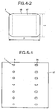
- Fig. 1-2 is a plan view for explaining a general configuration of a front surface (a light receiving surface) of the solar cell according to the first embodiment
- Fig. 1-3 is a plan view for explaining a general configuration of a back surface (a surface opposite to the light receiving surface) of the solar cell according to the first embodiment.
- Fig. 1-1 is a cross section taken along the line A-A of Fig. 1-3 .
- the solar cell according to the embodiment includes, as shown in Figs. 1-1 to 1-3 , a semiconductor layer 10 that is a photoelectric conversion layer including a p-type layer 11 that is a p-type silicon substrate as a semiconductor substrate, an n-type diffused layer 13 with a conductivity type inverse to that of the surface of the p-type layer 11, and a p+ layer (back surface field (BSF) layer) 14 containing a high concentration of impurity; an antireflective coating 15 provided on a light receiving surface of the semiconductor layer 10 to prevent the reflection of incident light; a front-surface silver electrode 21 that is a light receiving surface electrode provided on the light receiving surface of the semiconductor layer 10 substantially in the shape of a stick; an aluminum electrode 17 that is a back-surface electrode provided substantially all over the back surface of the semiconductor layer 10 to extract electric power and reflect the incident light; and a back-surface silver electrode 19 that is an extracting electrode that extracts the electric power from the aluminum electrode 17.
- a semiconductor layer 10 that is a
- the solar cell when sunlight irradiates the side of the light receiving surface (the side of the antireflective coating 15) of the solar cell and reaches a p-n junction surface (a junction surface of the p-type layer 11 and the n-type diffused layer 13) inside, a hole and electron pair on the p-n junction surface is separated.
- the separated electron moves toward the n-type diffused layer 13..
- the separated hole moves toward the p+ layer 14.
- Figs. 1-3 and 1-4 in the solar cell according to the embodiment, the aluminum electrode 17 and the back-surface silver electrode 19 are partially overlapped on the p+ layer 14.
- Fig. 1-4 is a schematic that depicts an enlargement of an area surrounding the back-surface silver electrode 19 shown in Fig. 1-3 , i.e., a schematic that depicts an enlargement of the partially overlapped area of the aluminum electrode 17 and the back-surface silver electrode 19 provided on the back surface of the solar cell.
- Fig. 1-5 is a schematic that depicts an enlargement of the area surrounding the back-surface silver electrode 19 shown in the cross section in Fig. 1-1 , i.e., a cross section of the surrounding area of a region B and a region C, where the aluminum electrode 17 and the back-surface silver electrode 19 are partially overlapped on the back surface of the solar cell.
- the back-surface silver electrode 19 presents a substantially square (rectangular) shape in the in-plane direction of the silicon substrate.
- the corners of the substantially square (rectangular) back-surface silver electrode 19 are curved.
- the back-surface silver electrode 19 is rounded off at the corners of the substantial square (rectangular) shape.
- the alloyed area 23 is reliably formed in the region B and the region C where the aluminum electrode 17 and the back-surface silver electrode 19 are partially overlapped, and also, the back-surface silver electrode 19 and the aluminum electrode 17 are reliably bonded even at the periphery of the back-surface silver electrode 19.
- the back-surface silver electrode 19 is of a substantially square (rectangular) shape in the in-plane direction of the silicon substrate, and the angle of each corner of the substantial square (rectangular) shape is substantially 90 degrees.
- the conventional solar cell also includes a region B' and a region C', where the aluminum electrode 17 and the back-surface silver electrode 19 are partially overlapped, as shown in Fig. 2 .
- the overlapped area is very fragile due to stress assumedly caused by difference in rate of thermal expansion between materials that occurs during rapid heating and cooling in firing of production process. Therefore, after the firing, in the region B' and the region C' where the aluminum electrode 17 and the back-surface silver electrode 19 are partially overlapped, the back-surface silver electrode 19 can separate from the aluminum electrode 17 at the corners of the back-surface silver electrode 19. The stress tends to concentrate at sharp corners of the back-surface silver electrode 19. Namely, the alloyed area 23 is not properly formed at the sharp corners of the back-surface silver electrode 19, and the separation of the back-surface silver electrode 19 tends to start from the 90-degree corner thereof.
- the corners are rounded off to remove sharp corners from the back-surface silver electrode 19 so that the stress does not concentrate on the corners of the back-surface silver electrode 19.
- the stress concentrated on the corners of the back-surface silver electrode 19 is eased, and the alloyed area 23 is reliably formed in the region B and the region C where the aluminum electrode 17 and the back-surface silver electrode 19 are partially overlapped as shown in Fig. 1-5 , which improves the bonding force between the aluminum electrode 17 and the back-surface silver electrode 19 and the substrate bonding force of the aluminum electrode 17 and the back-surface silver electrode 19. Therefore, according to the embodiment, a solar cell can be realized on which the back-surface silver electrode 19 is effectively prevented from separating from the aluminum electrode 17 by reliably bonding the back-surface silver electrode 19 and the aluminum electrode 17 even at the corners of the back-surface silver electrode 19.
- the warpage of the silicon substrate caused by different rates of thermal shrinkage between silicon and aluminum is larger compared with a thicker silicon substrate.
- the silicon substrate warps to a large extent, there is a problem that the silicon substrate cracks in the production process after the firing, resulting in a low production yield, or the production becomes impossible due to the crack in the silicon substrate.
- the back-surface silver electrode partially separates due to the different rates of thermal shrinkage between aluminum and silver depending on the materials combination.
- the back-surface silver electrode separates to a large extent, there is also a problem that the solar cell cracks due to stacking of the solar cells or the characteristics of the solar cell deteriorate, and thus the production yield decreases.
- the solar cell according to the embodiment it is possible to improve the bonding force between the aluminum electrode 17 and the back-surface silver electrode 19 and the bonding force of the aluminum electrode 17 and the back-surface silver electrode 19 with the silicon substrate, and thus the separation of the back-surface silver electrode 19 or the separation of the aluminum electrode 17 can be effectively prevented. This can ensure the bonding between the aluminum electrode 17 and the back-surface silver electrode 19 and the bonding of the aluminum electrode 17 and the back-surface silver electrode 19 with the substrate.
- the solar cell according to the embodiment does not cause many cracks on the silicon substrate differently from the conventional solar cell even when the thickness of the silicon substrate is reduced to lower the cost of the solar cell, and is applicable enough, whereby wider options and various types are available for the silver paste.
- the solar cell according to the embodiment has the back-surface silver electrode 19 rounded off at the sharp corners which exist in the back-surface silver electrode of the conventional solar cell, the area of the back-surface silver electrode 19 is smaller, and the amount of the silver paste used for the back-surface silver electrode 19 is reduced. Therefore, according to the embodiment, material costs can be reduced, and thus an inexpensive solar cell can be realized. Specific effects of the reduction of the silver paste will be described later.
- a method for producing the solar cell according to the embodiment configured as above is explained.
- a p-type silicon substrate 11' is sliced out of, for example, a p-type monocrystalline silicon ingot produced by the pulling method or a polycrystalline silicon ingot produced by the casting method.
- the silicon substrate 11' is etched by a thickness of about 10 to 20 micrometers using, for example, a few to 20 wt/% of sodium hydroxide or sodium carbonate, and a damaged layer and contamination produced on the silicon surface during slicing are removed.
- the silicon substrate 11' is washed using a mixed solution of hydrochloric acid and hydrogen peroxide to remove heavy metals such as iron attached on the surface of the substrate.
- An anisotropic etching is then performed using a solution made by adding isopropyl alcohol (IPA) to a similar low-concentrated alkaline solution to form a texture so that, for example, the surface of silicon (111) is exposed.
- IPA isopropyl alcohol
- an n-type diffused layer 13a is formed to form a p-n junction.
- phosphorus oxychloride (POCl 3 ) is used; a diffusion process is performed in a mixture gas atmosphere of nitrogen and oxygen at 800 to 900 degrees Celsius, and phosphorus is thermally diffused as shown in Fig. 3-2 to form the n-type diffused layer 13a with the inverse conductivity type all over the surface of the silicon substrate 11'.
- the sheet resistance of the n-type diffused layer 13a is, for example, several tens of (30 to 80) ohm/square, and the depth of the n-type diffused layer 13a is, for example, about 0.3 to 0.5 micrometer.
- n-type diffused layer 13a is formed on the back and side of the silicon substrate 11' by soaking the silicon substrate 11' in a solution of, for example, 20 wt/% potassium hydroxide for a few minutes. The resist is then removed by an organic solvent to obtain the silicon substrate 11' with the n-type diffused layer 13 formed all over the surface (light receiving surface) thereof as shown in Fig. 3-3 .
- the antireflective coating 15 made of a silicon oxide film, a silicon nitride film, or titanium oxide film is formed on the n-type diffused layer 13 in a uniform thickness.
- the antireflective coating 15 is formed by plasma CVD using silane (SiH 4 ) gas and ammonia (NH 3 ) gas as raw materials at a heating temperature equal to or higher than 300 degrees Celsius under reduced pressure.
- the refractive index is about 2.0 to 2.2
- the optimal thickness of the antireflective coating 15 is about 70 to 90 nanometers.
- the aluminum paste including glass is printed all over the back surface (the surface opposite to the light receiving surface) of the silicon substrate 11' using screen printing and dried as shown in Fig. 3-5 so that an aluminum paste layer 17a is formed all over the back surface of the silicon substrate 11'.
- the aluminum paste layer 17a has openings corresponding to the locations where the back-surface silver electrodes 19 are formed.
- the thickness of the applied aluminum paste can be adjusted according to the wire diameter that forms a screen mask, the thickness of emulsion, and the like.
- the silver paste for the back-surface silver electrodes 19 is printed on the back surface (the surface opposite to the light receiving surface) of the silicon substrate 11' on.which the aluminum electrode 17 is formed, and dried as shown in Fig. 3-6 so that a silver paste layer 19a is formed.
- the form of the silver paste layer 19a is a substantial square (rectangle) with the corners rounded off as shown in Fig. 1-3 .
- the silver paste can be printed using a screen mask with a pattern formed by an emulsion 27 on a mesh 25 as shown in Fig. 3-7 and Fig. 3-8 .
- the silver paste for the front-surface silver electrode 21 is printed on the front surface (the light receiving surface) of the silicon substrate 11' on which the antireflective coating 15 is formed, and dried so that a silver paste layer 21a is formed as shown in Fig. 3-9 .
- the thickness of the applied silver paste can also be adjusted according to the wire diameter of the mesh that forms a screen mask, the thickness of emulsion, and the like.
- the paste layers for the front and back electrodes are fired at the same time at 600 to 900 degrees Celsius for a few to a dozen minutes.
- the silver paste layer is fired to become the front-surface silver electrode 21 as shown in Fig. 3-10 ; at the same time, the silver material contacts the silicon in the silicon substrate 11' through the glass material included in the silver paste while the antireflective coating 15 is melting, and the antireflective coating 15 is solidified again. This secures the conductivity between the front-surface silver electrode 21 and the silicon.
- the process is generally called a fire-through process.
- the aluminum paste layer is fired to become the aluminum electrode 17 as shown in Fig. 3-10 , and the silver paste layer is burned to become the back-surface silver electrode 19 as shown in Fig. 3-10 .
- the aluminum in the aluminum paste reacts with the silicon in the silicon substrate 11' so that the p+ layer 14 is formed immediately below the aluminum electrode 17.
- the layer is generally called a back-surface field (BSF) layer, which contributes to the improvement of the energy conversion efficiency of the solar battery.
- BSF back-surface field
- an area between the n-type diffused layer 13 and the p+ layer 14 is made into the p-type layer 11.
- the silver paste reacts directly with the silicon in the silicon substrate 11' where the silver paste directly contacts the silicon substrate 11', and three metals including the silicon in the silicon substrate 11', the aluminum in the aluminum paste (the aluminum electrode 17), and the silver in the back-surface silver electrode 19 are partially alloyed where the silver paste contacts the aluminum paste.
- the cell is completed based on the method for producing the solar cell.
- a copper lead tab is provided on the silver electrode 3 to extract output power to the outside.
- the solar cell described above can be realized by changing only the shape of the back-surface silver electrode, that is, can be realized by changing only the shape of the mask to screen-print the silver paste for the back-surface silver electrode without changing existing equipment.
- Table 1 shows the reduced area of the back-surface silver electrode 19 and the reduction rate of the silver paste when the curvature radius R of the portion rounded off of the back-surface silver electrode 19 is changed from 1.0 millimeters to 3.0 millimeters in increments of 0.5 millimeters in the solar cell with the dimensions as described above.
- Table 1 Table 1 R (mm) Reduced area of back-surface silver electrode (mm 2 ) Reduction rate of silver paste (%) 3.0 7.7 10.1 2.5 5.4 7.0 2.0 3.4 4.5 1.5 1.9 2.5 1.0 0.9 1.1
- the embodiment of the present invention can reduce the amount of the silver paste for the back-surface silver electrode 19. Thereby, the cost of the materials can be reduced in the solar cell according to the embodiment, and an inexpensive solar cell can be realized.
- a solar cell according to another embodiment is explained in the chapter of a second embodiment.
- the second embodiment is not an embodiment of the present invention but helpful for understanding the present invention.
- the solar cell according to the second embodiment is configured basically in the same manner as the solar cell according to the first embodiment. Therefore, what are different between the solar cell according to the first embodiment and the solar cell according to the second embodiment are explained below.
- the components identical to those in the solar cell according to the first embodiment are denoted with the same reference numerals.
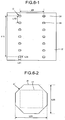
- Figs. 5-1 to 5-3 are schematics for explaining a general configuration of the solar cell according to the second embodiment.
- Fig. 5-1 corresponds to Fig. 1-3 , and is a plan view of the general configuration of the back surface (a surface opposite to the light receiving surface) of the solar cell according to the second embodiment.
- Fig. 5-2 corresponds to Fig. 1-4 , and is an enlarged schematic of the surrounding area of a back-surface silver electrode 31 shown in Fig. 5-1 , depicting the area where the aluminum electrode 17 provided on the back-surface of the solar cell and the back-surface silver electrode 31 are partially overlapped.
- Fig. 5-3 corresponds to Fig. 1-5 , and is an enlargement of the surrounding area of the back-surface silver electrode 31, depicting the cross section of the surrounding area of a region D and a region E, where the aluminum electrode 17 provided on the back surface of the solar cell and the back-surface silver electrode 31 are partially overlapped. Because the cross section and the light receiving surface (front surface) of the solar cell are configured identically to those in the first embodiment, Figs. 1-1 and 1-2 are referenced here.
- the back-surface silver electrode 31 according to the second embodiment corresponds to the back-surface silver electrode 19 according to the first embodiment; however, as shown in Figs. 5-1 and 5-2 , the back-surface silver electrode 31 is different in that the corners are chamfered instead of being rounded off.
- the back-surface silver electrode 31 presents a substantially square (rectangular) shape in the in-plane direction of the silicon substrate.
- the back-surface silver electrode 31 is chamfered at the corners of the substantially square (rectangular) shape.
- the shape of the corners of the back-surface silver electrode is different from that in the first embodiment, in the region D and the region E where the aluminum electrode 17 and the back-surface silver electrode 31 are partially overlapped, three metals of silicon in the p+ layer 14 of the silicon substrate, aluminum in the aluminum electrode 17, and silver in the back-surface silver electrode 31 are partially alloyed so that an alloyed area 33 is formed as shown in Figs. 5-2 and 5-3. While borders of the metals (the silicon, the aluminum, and the silver) in the region D and the region E are clearly defined in Fig. 5-3 , it is needless to say that the regions are partially alloyed and actually not clear.
- the alloyed area 33 is reliably formed in the region D and the region E where the aluminum electrode 17 and the back-surface silver electrode 31 are partially overlapped as shown in Fig. 5-3 , and the back-surface silver electrode 31 and the aluminum electrode 17 are reliably bonded at the edges of the back-surface silver electrode 31.
- the corners of the back-surface silver electrode 31 are chamfered to remove any sharp edges so that a stress is not concentrated on the corners of the back-surface silver electrode 31.
- This can relieve the stress concentrated at the corners of the back-surface silver electrode 31, ensures that the alloyed area 33 is formed in the region D and the region E where the aluminum electrode 17 and the back-surface silver electrode 31 are partially overlapped as shown in Fig. 5-3 , and thus increases the bonding force between the aluminum electrode 17 and the back-surface silver electrode 31 and the substrate bonding force of the aluminum electrode 17 and the back-surface silver electrode 31. Therefore, according to the embodiment, a solar cell can be realized that reliably bonds the back-surface silver electrode 19 and the aluminum electrode 17 at the corners of the back-surface silver electrode 19 to effectively prevent the separation of the back-surface silver electrode 19 from the aluminum electrode 17.
- a chamfered dimension C is larger than the alloyed area 33, a part of the alloyed area of the aluminum electrode 17 and the back-surface silver electrode 31 cannot be formed.
- Such an electrode is not suitable as the back-surface silver electrode 31.
- dimensions L21 and L23 where the aluminum electrode 17 and the back-surface silver electrode 31 are overlapped in the longitudinal direction of the back-surface silver electrode 31 and dimensions L25 and L27 where the aluminum electrode 17 and the back-surface silver electrode 31 are overlapped in the short-side direction of the back-surface silver electrode 31 that determine the dimension of the alloyed area 33 need to be determined so as to reliably form the alloyed area 33.
- the dimensions should be determined with consideration of the pattern misalignment of the aluminum paste and the silver paste at the time of screen printing.
- the solar cell according to the embodiment can also ensure the bonding between the aluminum electrode 17 and the back-surface silver electrode 31 and the bonding between the substrate and the aluminum electrode 17 as well as the back-surface silver electrode 31 as described above. Therefore, in the solar cell according to the embodiment, even when the thickness of the silicon substrate is reduced to lower the cost the solar cell, the silicon substrate will not have many cracks differently from the conventional solar cell, and wider options and various types are available for the silver paste.
- the solar cell according to the embodiment has the sharp corners of the back-surface silver electrode 31 chamfered, the area of the back-surface silver electrode 31 is smaller, which reduces the amount of the silver paste used for the back-surface silver electrode 31 compared to the conventional solar cell where such sharp corners exist in the back-surface silver electrode.
- the second embodiment it is also possible to reduce material costs, and thus realize an inexpensive solar cell.
- the solar cell according to the embodiment can be produced in the same process as in the first embodiment except that the silver paste is screen-printed in the substantially square (rectangular) shape with chamfered corners as shown in Fig. 5-1 .
- the solar cell according to the embodiment also can be realized by changing the shape of the back-surface silver electrode, namely by changing only the shape of the mask for screen-printing the back-surface silver electrode with the silver paste without modifying the existing facilities.
- Length L21 of the long side of the back-surface silver electrode 31 9.8 millimeters
- Table 2 depicts the reduced area of the back-surface silver electrode 31 and the reduction rate of the silver paste when the chamfered dimension C of the chamfered portion of the back-surface silver electrode 31 is changed from 1.0 millimeters to 3.0 millimeters in increments of 0.5 millimeters in the solar cell with the dimensions as described above.
- Table 2 Table 2 c (mm) Reduced area of back-surface silver electrode (mm 2 ) Reduction rate of silver paste (%) 3.0 18.0 23.5 2.5 12.5 16.4 2.0 8.0 10.5 1.5 4.5 5.9 1.0 2.0 2.6
- the embodiment of the present invention can reduce the amount of the silver paste for the back-surface silver electrode 31. Thereby, the cost of the material can be reduced in the solar cell according to the embodiment, and an inexpensive solar cell can be realized.
- the curvature radius or the chamfered dimension needs to be large to reduce more amount of the silver paste; however, too large curvature radius or chamfered dimension prevents forming the alloyed area of aluminum and silver.
- pattern misalignment that occurs on screen-printing the pastes for the aluminum electrode and the silver electrode should be considered so that the alloyed area is formed reliably.
- the solar cells according to the first embodiment is an example of the present invention.
- the present invention is not limited by the embodiments, but is susceptible to various changes and modifications without departing from the scope of the present invention.
- the solar cell according to the present invention is useful as a solar cell configured with an aluminum electrode and a silver electrode for extracting electric power partially overlapped with each other.
Priority Applications (1)
| Application Number | Priority Date | Filing Date | Title |
|---|---|---|---|
| EP10001436.4A EP2219227B1 (en) | 2005-11-28 | 2005-11-28 | Solar cell |
Applications Claiming Priority (1)
| Application Number | Priority Date | Filing Date | Title |
|---|---|---|---|
| PCT/JP2005/021782 WO2007060743A1 (ja) | 2005-11-28 | 2005-11-28 | 太陽電池セル |
Related Child Applications (2)
| Application Number | Title | Priority Date | Filing Date |
|---|---|---|---|
| EP10001436.4A Division-Into EP2219227B1 (en) | 2005-11-28 | 2005-11-28 | Solar cell |
| EP10001436.4A Division EP2219227B1 (en) | 2005-11-28 | 2005-11-28 | Solar cell |
Publications (3)
| Publication Number | Publication Date |
|---|---|
| EP1870942A1 EP1870942A1 (en) | 2007-12-26 |
| EP1870942A4 EP1870942A4 (en) | 2010-09-15 |
| EP1870942B1 true EP1870942B1 (en) | 2016-08-24 |
Family
ID=38066985
Family Applications (2)
| Application Number | Title | Priority Date | Filing Date |
|---|---|---|---|
| EP05809633.0A Expired - Fee Related EP1870942B1 (en) | 2005-11-28 | 2005-11-28 | Solar cell |
| EP10001436.4A Expired - Fee Related EP2219227B1 (en) | 2005-11-28 | 2005-11-28 | Solar cell |
Family Applications After (1)
| Application Number | Title | Priority Date | Filing Date |
|---|---|---|---|
| EP10001436.4A Expired - Fee Related EP2219227B1 (en) | 2005-11-28 | 2005-11-28 | Solar cell |
Country Status (6)
| Country | Link |
|---|---|
| US (2) | US20080105297A1 (un) |
| EP (2) | EP1870942B1 (un) |
| JP (1) | JP4343225B2 (un) |
| CN (1) | CN101088167B (un) |
| HK (1) | HK1111807A1 (un) |
| WO (1) | WO2007060743A1 (un) |
Families Citing this family (15)
| Publication number | Priority date | Publication date | Assignee | Title |
|---|---|---|---|---|
| EP1870942B1 (en) * | 2005-11-28 | 2016-08-24 | Mitsubishi Electric Corporation | Solar cell |
| EP2180522B1 (en) * | 2007-07-30 | 2018-02-07 | Kyocera Corporation | Solar cell module |
| WO2009122977A1 (ja) * | 2008-03-31 | 2009-10-08 | シャープ株式会社 | 太陽電池、太陽電池ストリングおよび太陽電池モジュール |
| WO2009139390A1 (ja) * | 2008-05-15 | 2009-11-19 | 株式会社アルバック | 薄膜太陽電池モジュール及びその製造方法 |
| EP2293349A4 (en) * | 2008-06-23 | 2014-10-22 | Mitsubishi Electric Corp | PHOTOVOLTAIC SYSTEM AND METHOD FOR MANUFACTURING THE SAME |
| JP5154516B2 (ja) * | 2009-05-22 | 2013-02-27 | シャープ株式会社 | 太陽電池モジュール及び太陽電池モジュールの製造方法 |
| CN102576776B (zh) * | 2009-07-22 | 2015-07-22 | 三菱电机株式会社 | 太阳能电池单元及其制造方法 |
| EP2500948A4 (en) * | 2009-11-13 | 2015-10-14 | Mitsubishi Electric Corp | SOLAR CELL |
| WO2012026358A1 (ja) * | 2010-08-24 | 2012-03-01 | 三洋電機株式会社 | 太陽電池及びその製造方法 |
| WO2012115006A1 (ja) * | 2011-02-21 | 2012-08-30 | シャープ株式会社 | スクリーンおよび太陽電池の製造方法 |
| DE102011001998A1 (de) | 2011-04-12 | 2012-10-18 | Schott Solar Ag | Solarzelle |
| DE102011001999A1 (de) | 2011-04-12 | 2012-10-18 | Schott Solar Ag | Solarzelle |
| EP2757591B1 (en) * | 2011-09-13 | 2017-08-23 | Kyocera Corporation | Solar cell module |
| DE102013212845A1 (de) * | 2013-07-02 | 2015-01-08 | Solarworld Industries Sachsen Gmbh | Photovoltaikmodul |
| DE102013107174B4 (de) * | 2013-07-08 | 2019-10-31 | Solarworld Industries Gmbh | Solarzelle und Solarzellenmodul |
Citations (3)
| Publication number | Priority date | Publication date | Assignee | Title |
|---|---|---|---|---|
| US5118362A (en) * | 1990-09-24 | 1992-06-02 | Mobil Solar Energy Corporation | Electrical contacts and methods of manufacturing same |
| JPH1134473A (ja) * | 1997-07-16 | 1999-02-09 | Sumitomo Kinzoku Erekutorodebaisu:Kk | パターン印刷方法 |
| JP2003273378A (ja) * | 2002-03-15 | 2003-09-26 | Kyocera Corp | 太陽電池素子 |
Family Cites Families (15)
| Publication number | Priority date | Publication date | Assignee | Title |
|---|---|---|---|---|
| US4127424A (en) * | 1976-12-06 | 1978-11-28 | Ses, Incorporated | Photovoltaic cell array |
| US4320251A (en) * | 1980-07-28 | 1982-03-16 | Solamat Inc. | Ohmic contacts for solar cells by arc plasma spraying |
| EP0542961B1 (en) | 1991-06-11 | 1998-04-01 | Ase Americas, Inc. | Improved solar cell and method of making same |
| US5320684A (en) * | 1992-05-27 | 1994-06-14 | Mobil Solar Energy Corporation | Solar cell and method of making same |
| TW387152B (en) * | 1996-07-24 | 2000-04-11 | Tdk Corp | Solar battery and manufacturing method thereof |
| JP3349370B2 (ja) * | 1996-11-12 | 2002-11-25 | シャープ株式会社 | 太陽電池セル |
| JPH10335267A (ja) * | 1997-05-30 | 1998-12-18 | Mitsubishi Electric Corp | 半導体装置の製造方法 |
| JP4026294B2 (ja) * | 2000-03-07 | 2007-12-26 | 豊田合成株式会社 | Iii族窒化物系化合物半導体素子の製造方法 |
| JP4979154B2 (ja) * | 2000-06-07 | 2012-07-18 | ルネサスエレクトロニクス株式会社 | 半導体装置 |
| JP3957461B2 (ja) * | 2001-01-22 | 2007-08-15 | シャープ株式会社 | 太陽電池セルおよびその製造方法 |
| JP2002289634A (ja) | 2001-03-23 | 2002-10-04 | Citizen Watch Co Ltd | 半導体装置およびその製造方法 |
| JP2003273379A (ja) * | 2002-03-15 | 2003-09-26 | Kyocera Corp | 太陽電池素子 |
| US6829134B2 (en) | 2002-07-09 | 2004-12-07 | Murata Manufacturing Co., Ltd. | Laminated ceramic electronic component and method for manufacturing the same |
| JP4401158B2 (ja) * | 2003-12-16 | 2010-01-20 | シャープ株式会社 | 太陽電池の製造方法 |
| EP1870942B1 (en) * | 2005-11-28 | 2016-08-24 | Mitsubishi Electric Corporation | Solar cell |
-
2005
- 2005-11-28 EP EP05809633.0A patent/EP1870942B1/en not_active Expired - Fee Related
- 2005-11-28 JP JP2006517869A patent/JP4343225B2/ja active Active
- 2005-11-28 CN CN2005800174534A patent/CN101088167B/zh active Active
- 2005-11-28 WO PCT/JP2005/021782 patent/WO2007060743A1/ja active Application Filing
- 2005-11-28 EP EP10001436.4A patent/EP2219227B1/en not_active Expired - Fee Related
- 2005-11-28 US US11/547,656 patent/US20080105297A1/en not_active Abandoned
-
2008
- 2008-03-05 HK HK08102548.5A patent/HK1111807A1/xx not_active IP Right Cessation
-
2010
- 2010-04-08 US US12/756,388 patent/US8173895B2/en not_active Expired - Fee Related
Patent Citations (3)
| Publication number | Priority date | Publication date | Assignee | Title |
|---|---|---|---|---|
| US5118362A (en) * | 1990-09-24 | 1992-06-02 | Mobil Solar Energy Corporation | Electrical contacts and methods of manufacturing same |
| JPH1134473A (ja) * | 1997-07-16 | 1999-02-09 | Sumitomo Kinzoku Erekutorodebaisu:Kk | パターン印刷方法 |
| JP2003273378A (ja) * | 2002-03-15 | 2003-09-26 | Kyocera Corp | 太陽電池素子 |
Also Published As
| Publication number | Publication date |
|---|---|
| JPWO2007060743A1 (ja) | 2009-05-07 |
| EP2219227A2 (en) | 2010-08-18 |
| CN101088167B (zh) | 2011-07-06 |
| CN101088167A (zh) | 2007-12-12 |
| EP1870942A1 (en) | 2007-12-26 |
| JP4343225B2 (ja) | 2009-10-14 |
| HK1111807A1 (en) | 2008-08-15 |
| EP1870942A4 (en) | 2010-09-15 |
| US8173895B2 (en) | 2012-05-08 |
| US20100193028A1 (en) | 2010-08-05 |
| US20080105297A1 (en) | 2008-05-08 |
| EP2219227B1 (en) | 2017-06-07 |
| EP2219227A3 (en) | 2010-12-08 |
| WO2007060743A1 (ja) | 2007-05-31 |
Similar Documents
| Publication | Publication Date | Title |
|---|---|---|
| EP1870942B1 (en) | Solar cell | |
| US8450602B2 (en) | Solar cell and manufacturing method thereof | |
| JP5174903B2 (ja) | 太陽電池セルの製造方法 | |
| US8106291B2 (en) | Solar battery and manufacturing method therefor | |
| KR101719949B1 (ko) | 태양전지 셀 및 그 제조 방법, 태양전지 모듈 | |
| JP4334455B2 (ja) | 太陽電池モジュール | |
| JP4656996B2 (ja) | 太陽電池 | |
| JPWO2008090718A1 (ja) | 太陽電池セル、太陽電池アレイおよび太陽電池モジュール | |
| JP2007266262A (ja) | インターコネクタ付き太陽電池、太陽電池モジュールおよび太陽電池モジュールの製造方法 | |
| WO2009081684A1 (ja) | 光電変換装置および光電変換装置の製造方法 | |
| JP2010135562A (ja) | 光電変換素子、光電変換素子モジュールおよび光電変換素子の製造方法 | |
| JP2009290235A (ja) | 太陽電池セルおよびその製造方法 | |
| JP2003224289A (ja) | 太陽電池、太陽電池の接続方法、及び太陽電池モジュール | |
| EP1826825A1 (en) | Solar cell structure comprising rear contacts and current collection by means of transistor effect and production method thereof | |
| JP4467337B2 (ja) | 太陽電池モジュール | |
| JP2005260157A (ja) | 太陽電池セルおよび太陽電池モジュール | |
| JP5029921B2 (ja) | 太陽電池セルの製造方法 | |
| JP5363666B2 (ja) | 太陽電池セルおよびその製造方法 | |
| WO2009150741A1 (ja) | 光起電力装置の製造方法 | |
| KR20190043291A (ko) | 분할셀 및 포일을 이용한 태양전지 모듈 | |
| JP2009071340A (ja) | 太陽電池モジュール | |
| JP2011003784A (ja) | 太陽電池セルおよびその製造方法 |
Legal Events
| Date | Code | Title | Description |
|---|---|---|---|
| PUAI | Public reference made under article 153(3) epc to a published international application that has entered the european phase |
Free format text: ORIGINAL CODE: 0009012 |
|
| 17P | Request for examination filed |
Effective date: 20061005 |
|
| AK | Designated contracting states |
Kind code of ref document: A1 Designated state(s): AT BE BG CH CY CZ DE DK EE ES FI FR GB GR HU IE IS IT LI LT LU LV MC NL PL PT RO SE SI SK TR |
|
| AX | Request for extension of the european patent |
Extension state: AL BA HR MK YU |
|
| RBV | Designated contracting states (corrected) |
Designated state(s): DE ES IT |
|
| DAX | Request for extension of the european patent (deleted) | ||
| A4 | Supplementary search report drawn up and despatched |
Effective date: 20100816 |
|
| 17Q | First examination report despatched |
Effective date: 20130801 |
|
| REG | Reference to a national code |
Ref country code: DE Ref legal event code: R079 Ref document number: 602005050084 Country of ref document: DE Free format text: PREVIOUS MAIN CLASS: H01L0031022400 Ipc: H01L0031050000 |
|
| GRAP | Despatch of communication of intention to grant a patent |
Free format text: ORIGINAL CODE: EPIDOSNIGR1 |
|
| RIC1 | Information provided on ipc code assigned before grant |
Ipc: H01L 31/05 20060101AFI20160304BHEP Ipc: H01L 31/0224 20060101ALI20160304BHEP |
|
| INTG | Intention to grant announced |
Effective date: 20160322 |
|
| GRAS | Grant fee paid |
Free format text: ORIGINAL CODE: EPIDOSNIGR3 |
|
| GRAA | (expected) grant |
Free format text: ORIGINAL CODE: 0009210 |
|
| RIN1 | Information on inventor provided before grant (corrected) |
Inventor name: KARAKIDA, SHOICHI Inventor name: NAKATANI, MITSUNORI Inventor name: NISHIDA, TAKAHIKO Inventor name: MORIKAWA, HIROAKI |
|
| AK | Designated contracting states |
Kind code of ref document: B1 Designated state(s): DE ES IT |
|
| REG | Reference to a national code |
Ref country code: DE Ref legal event code: R096 Ref document number: 602005050084 Country of ref document: DE |
|
| PG25 | Lapsed in a contracting state [announced via postgrant information from national office to epo] |
Ref country code: IT Free format text: LAPSE BECAUSE OF FAILURE TO SUBMIT A TRANSLATION OF THE DESCRIPTION OR TO PAY THE FEE WITHIN THE PRESCRIBED TIME-LIMIT Effective date: 20160824 |
|
| PG25 | Lapsed in a contracting state [announced via postgrant information from national office to epo] |
Ref country code: ES Free format text: LAPSE BECAUSE OF FAILURE TO SUBMIT A TRANSLATION OF THE DESCRIPTION OR TO PAY THE FEE WITHIN THE PRESCRIBED TIME-LIMIT Effective date: 20160824 |
|
| REG | Reference to a national code |
Ref country code: DE Ref legal event code: R097 Ref document number: 602005050084 Country of ref document: DE |
|
| PLBE | No opposition filed within time limit |
Free format text: ORIGINAL CODE: 0009261 |
|
| STAA | Information on the status of an ep patent application or granted ep patent |
Free format text: STATUS: NO OPPOSITION FILED WITHIN TIME LIMIT |
|
| 26N | No opposition filed |
Effective date: 20170526 |
|
| PGFP | Annual fee paid to national office [announced via postgrant information from national office to epo] |
Ref country code: DE Payment date: 20171121 Year of fee payment: 13 |
|
| REG | Reference to a national code |
Ref country code: DE Ref legal event code: R119 Ref document number: 602005050084 Country of ref document: DE |
|
| PG25 | Lapsed in a contracting state [announced via postgrant information from national office to epo] |
Ref country code: DE Free format text: LAPSE BECAUSE OF NON-PAYMENT OF DUE FEES Effective date: 20190601 |