EP1868250A2 - Photovoltaic module with integrated current collection and interconnection - Google Patents
Photovoltaic module with integrated current collection and interconnection Download PDFInfo
- Publication number
- EP1868250A2 EP1868250A2 EP07252359A EP07252359A EP1868250A2 EP 1868250 A2 EP1868250 A2 EP 1868250A2 EP 07252359 A EP07252359 A EP 07252359A EP 07252359 A EP07252359 A EP 07252359A EP 1868250 A2 EP1868250 A2 EP 1868250A2
- Authority
- EP
- European Patent Office
- Prior art keywords
- photovoltaic cell
- carrier
- conductor
- module
- sheet
- Prior art date
- Legal status (The legal status is an assumption and is not a legal conclusion. Google has not performed a legal analysis and makes no representation as to the accuracy of the status listed.)
- Granted
Links
- 239000004020 conductor Substances 0.000 claims abstract description 104
- 239000000463 material Substances 0.000 claims description 36
- 150000001336 alkenes Chemical class 0.000 claims description 23
- JRZJOMJEPLMPRA-UHFFFAOYSA-N olefin Natural products CCCCCCCC=C JRZJOMJEPLMPRA-UHFFFAOYSA-N 0.000 claims description 22
- 239000004033 plastic Substances 0.000 claims description 20
- 229920003023 plastic Polymers 0.000 claims description 20
- 238000000034 method Methods 0.000 claims description 8
- 239000012528 membrane Substances 0.000 claims description 7
- 229920000642 polymer Polymers 0.000 claims description 5
- 238000002161 passivation Methods 0.000 claims description 4
- 238000004519 manufacturing process Methods 0.000 claims description 2
- 239000010408 film Substances 0.000 description 34
- 229910017612 Cu(In,Ga)Se2 Inorganic materials 0.000 description 7
- 239000000853 adhesive Substances 0.000 description 7
- 230000001070 adhesive effect Effects 0.000 description 7
- 239000004065 semiconductor Substances 0.000 description 6
- 239000000758 substrate Substances 0.000 description 6
- 238000009434 installation Methods 0.000 description 5
- 239000002861 polymer material Substances 0.000 description 5
- 229910000679 solder Inorganic materials 0.000 description 5
- RYGMFSIKBFXOCR-UHFFFAOYSA-N Copper Chemical compound [Cu] RYGMFSIKBFXOCR-UHFFFAOYSA-N 0.000 description 4
- 229910052802 copper Inorganic materials 0.000 description 4
- 239000010949 copper Substances 0.000 description 4
- XUIMIQQOPSSXEZ-UHFFFAOYSA-N Silicon Chemical compound [Si] XUIMIQQOPSSXEZ-UHFFFAOYSA-N 0.000 description 3
- 229910045601 alloy Inorganic materials 0.000 description 3
- 239000000956 alloy Substances 0.000 description 3
- 229910052782 aluminium Inorganic materials 0.000 description 3
- XAGFODPZIPBFFR-UHFFFAOYSA-N aluminium Chemical compound [Al] XAGFODPZIPBFFR-UHFFFAOYSA-N 0.000 description 3
- 239000000969 carrier Substances 0.000 description 3
- 238000004049 embossing Methods 0.000 description 3
- 238000001125 extrusion Methods 0.000 description 3
- 239000011521 glass Substances 0.000 description 3
- 239000000976 ink Substances 0.000 description 3
- -1 polyethylene Polymers 0.000 description 3
- 229910052710 silicon Inorganic materials 0.000 description 3
- 239000010703 silicon Substances 0.000 description 3
- 239000010935 stainless steel Substances 0.000 description 3
- 229910001220 stainless steel Inorganic materials 0.000 description 3
- PXHVJJICTQNCMI-UHFFFAOYSA-N Nickel Chemical compound [Ni] PXHVJJICTQNCMI-UHFFFAOYSA-N 0.000 description 2
- BQCADISMDOOEFD-UHFFFAOYSA-N Silver Chemical compound [Ag] BQCADISMDOOEFD-UHFFFAOYSA-N 0.000 description 2
- XLOMVQKBTHCTTD-UHFFFAOYSA-N Zinc monoxide Chemical compound [Zn]=O XLOMVQKBTHCTTD-UHFFFAOYSA-N 0.000 description 2
- 239000010426 asphalt Substances 0.000 description 2
- 238000005520 cutting process Methods 0.000 description 2
- 239000011888 foil Substances 0.000 description 2
- 229910052751 metal Inorganic materials 0.000 description 2
- 239000002184 metal Substances 0.000 description 2
- 238000012986 modification Methods 0.000 description 2
- 230000004048 modification Effects 0.000 description 2
- 238000007747 plating Methods 0.000 description 2
- 239000011120 plywood Substances 0.000 description 2
- 238000007639 printing Methods 0.000 description 2
- 229910052709 silver Inorganic materials 0.000 description 2
- 239000004332 silver Substances 0.000 description 2
- 238000005476 soldering Methods 0.000 description 2
- 229920001169 thermoplastic Polymers 0.000 description 2
- OKTJSMMVPCPJKN-UHFFFAOYSA-N Carbon Chemical compound [C] OKTJSMMVPCPJKN-UHFFFAOYSA-N 0.000 description 1
- 229910004613 CdTe Inorganic materials 0.000 description 1
- 229910001218 Gallium arsenide Inorganic materials 0.000 description 1
- ZOKXTWBITQBERF-UHFFFAOYSA-N Molybdenum Chemical compound [Mo] ZOKXTWBITQBERF-UHFFFAOYSA-N 0.000 description 1
- 239000004698 Polyethylene Substances 0.000 description 1
- 239000004743 Polypropylene Substances 0.000 description 1
- 229910007116 SnPb Inorganic materials 0.000 description 1
- 229920006355 Tefzel Polymers 0.000 description 1
- NIXOWILDQLNWCW-UHFFFAOYSA-N acrylic acid group Chemical group C(C=C)(=O)O NIXOWILDQLNWCW-UHFFFAOYSA-N 0.000 description 1
- 229920006397 acrylic thermoplastic Polymers 0.000 description 1
- 229910021417 amorphous silicon Inorganic materials 0.000 description 1
- 229910052799 carbon Inorganic materials 0.000 description 1
- 230000015556 catabolic process Effects 0.000 description 1
- 229910010293 ceramic material Inorganic materials 0.000 description 1
- 229910017052 cobalt Inorganic materials 0.000 description 1
- 239000010941 cobalt Substances 0.000 description 1
- GUTLYIVDDKVIGB-UHFFFAOYSA-N cobalt atom Chemical compound [Co] GUTLYIVDDKVIGB-UHFFFAOYSA-N 0.000 description 1
- 229910021419 crystalline silicon Inorganic materials 0.000 description 1
- 230000007547 defect Effects 0.000 description 1
- 238000006731 degradation reaction Methods 0.000 description 1
- 230000008021 deposition Effects 0.000 description 1
- 239000000975 dye Substances 0.000 description 1
- 239000012777 electrically insulating material Substances 0.000 description 1
- 238000007772 electroless plating Methods 0.000 description 1
- 238000009713 electroplating Methods 0.000 description 1
- 238000005538 encapsulation Methods 0.000 description 1
- 230000006353 environmental stress Effects 0.000 description 1
- QHSJIZLJUFMIFP-UHFFFAOYSA-N ethene;1,1,2,2-tetrafluoroethene Chemical compound C=C.FC(F)=C(F)F QHSJIZLJUFMIFP-UHFFFAOYSA-N 0.000 description 1
- 229920002313 fluoropolymer Polymers 0.000 description 1
- 239000004811 fluoropolymer Substances 0.000 description 1
- 238000007646 gravure printing Methods 0.000 description 1
- AMGQUBHHOARCQH-UHFFFAOYSA-N indium;oxotin Chemical compound [In].[Sn]=O AMGQUBHHOARCQH-UHFFFAOYSA-N 0.000 description 1
- 239000011810 insulating material Substances 0.000 description 1
- 230000001788 irregular Effects 0.000 description 1
- 239000000203 mixture Substances 0.000 description 1
- 229910052750 molybdenum Inorganic materials 0.000 description 1
- 239000011733 molybdenum Substances 0.000 description 1
- 229910052759 nickel Inorganic materials 0.000 description 1
- 229920003229 poly(methyl methacrylate) Polymers 0.000 description 1
- 229920001748 polybutylene Polymers 0.000 description 1
- 229920000573 polyethylene Polymers 0.000 description 1
- 229920006254 polymer film Polymers 0.000 description 1
- 229920001155 polypropylene Polymers 0.000 description 1
- 229920001296 polysiloxane Polymers 0.000 description 1
- 229920002620 polyvinyl fluoride Polymers 0.000 description 1
- 238000004321 preservation Methods 0.000 description 1
- 238000003825 pressing Methods 0.000 description 1
- 229920005989 resin Polymers 0.000 description 1
- 239000011347 resin Substances 0.000 description 1
- 238000010022 rotary screen printing Methods 0.000 description 1
- 239000002904 solvent Substances 0.000 description 1
- 125000006850 spacer group Chemical group 0.000 description 1
- ISXSCDLOGDJUNJ-UHFFFAOYSA-N tert-butyl prop-2-enoate Chemical compound CC(C)(C)OC(=O)C=C ISXSCDLOGDJUNJ-UHFFFAOYSA-N 0.000 description 1
- 230000008646 thermal stress Effects 0.000 description 1
- 239000004416 thermosoftening plastic Substances 0.000 description 1
- 239000010409 thin film Substances 0.000 description 1
- 239000011787 zinc oxide Substances 0.000 description 1
Images


Classifications
-
- H—ELECTRICITY
- H01—ELECTRIC ELEMENTS
- H01L—SEMICONDUCTOR DEVICES NOT COVERED BY CLASS H10
- H01L31/00—Semiconductor devices sensitive to infrared radiation, light, electromagnetic radiation of shorter wavelength or corpuscular radiation and specially adapted either for the conversion of the energy of such radiation into electrical energy or for the control of electrical energy by such radiation; Processes or apparatus specially adapted for the manufacture or treatment thereof or of parts thereof; Details thereof
- H01L31/04—Semiconductor devices sensitive to infrared radiation, light, electromagnetic radiation of shorter wavelength or corpuscular radiation and specially adapted either for the conversion of the energy of such radiation into electrical energy or for the control of electrical energy by such radiation; Processes or apparatus specially adapted for the manufacture or treatment thereof or of parts thereof; Details thereof adapted as photovoltaic [PV] conversion devices
- H01L31/042—PV modules or arrays of single PV cells
- H01L31/05—Electrical interconnection means between PV cells inside the PV module, e.g. series connection of PV cells
- H01L31/0504—Electrical interconnection means between PV cells inside the PV module, e.g. series connection of PV cells specially adapted for series or parallel connection of solar cells in a module
- H01L31/0508—Electrical interconnection means between PV cells inside the PV module, e.g. series connection of PV cells specially adapted for series or parallel connection of solar cells in a module the interconnection means having a particular shape
-
- Y—GENERAL TAGGING OF NEW TECHNOLOGICAL DEVELOPMENTS; GENERAL TAGGING OF CROSS-SECTIONAL TECHNOLOGIES SPANNING OVER SEVERAL SECTIONS OF THE IPC; TECHNICAL SUBJECTS COVERED BY FORMER USPC CROSS-REFERENCE ART COLLECTIONS [XRACs] AND DIGESTS
- Y02—TECHNOLOGIES OR APPLICATIONS FOR MITIGATION OR ADAPTATION AGAINST CLIMATE CHANGE
- Y02E—REDUCTION OF GREENHOUSE GAS [GHG] EMISSIONS, RELATED TO ENERGY GENERATION, TRANSMISSION OR DISTRIBUTION
- Y02E10/00—Energy generation through renewable energy sources
- Y02E10/50—Photovoltaic [PV] energy
Definitions
- the present invention relates generally to a photovoltaic device and more particularly to photovoltaic modules having an integrated current collection and interconnection configuration.
- PV photovoltaic
- Alternative current collection methods involve conductive wires that are placed in contact with the cell.
- PV cells are interconnected by using the so-called "tab and string” technique of soldering two or three conductive ribbons between the front and back surfaces of adjacent cells.
- Alternative interconnect configurations include shingled interconnects with conductive adhesives.
- Some prior art PV devices also include embossing of an adhesive backed metal foil to enhance conductivity of the substrate of the device.
- One embodiment of the invention includes a photovoltaic module comprising a first photovoltaic cell, a second photovoltaic cell, and a collector-connector which is configured to collect current from the first photovoltaic cell and to electrically connect the first photovoltaic cell with the second photovoltaic cell.
- Another embodiment of the invention includes a photovoltaic module comprising a first photovoltaic cell, a second photovoltaic cell, and an interconnect comprising an electrically insulating carrier and at least one electrical conductor which electrically connects the first photovoltaic cell to the second photovoltaic cell.
- Another embodiment of the invention includes a photovoltaic module comprising a first thermal plastic olefin sheet, a second flexible membrane roofing sheet, a plurality photovoltaic cells located between the first and the second sheets, and a plurality of electrical conductors which electrically interconnect the plurality of photovoltaic cells.
- Figures 1-12B are schematic illustrations of the components of photovoltaic modules of the embodiments of the invention.
- Figures 1, 2A, 2B, 3C, 4B, 4C, 5B, 6C, 6E, 9B, 8A, 8B, 10, 11 and 12A are side cross sectional views.
- Figures 3A, 5A, 7A and 9A are three dimensional views.
- Figures 3B, 4A, 5C, 6A, 6B, 6D, 7B-7D and 12B are top views. The dimensions of the components in the Figures are not necessarily to scale.
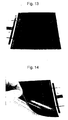
- FIGS 13 and 14 are photographs of photovoltaic cells according to the examples of the invention.
- One embodiment of the invention provides a photovoltaic module including at least two photovoltaic cells and a collector-connector.
- the term “module” includes an assembly of at least two, and preferably three or more electrically interconnected photovoltaic cells, which may also be referred to as "solar cells”.
- the "collector-connector” is a device that acts as both a current collector to collect current from at least one photovoltaic cell of the module, and as an interconnect which electrically interconnects the at least one photovoltaic cell with at least one other photovoltaic cell of the module.
- the collector-connector takes the current collected from each cell of the module and combines it to provide a useful current and voltage at the output connectors of the module.
- a photovoltaic module which includes an interconnect comprising an electrically insulating carrier and at least one electrical conductor which electrically connects one photovoltaic cell to at least one other photovoltaic cell of the module.
- this interconnect comprises the collector-connector which acts as both a current collector to collect current from at least one photovoltaic cell of the module and as an interconnect which electrically interconnects the at least one photovoltaic cell with at least one other photovoltaic cell of the module.
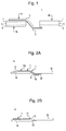
- FIG 1 schematically illustrates a module 1 of the first and second embodiments of the invention.
- the module 1 includes first and second photovoltaic cells 3a and 3b. It should be understood that the module 1 may contain three or more cells, such as 3-10,000 cells for example.
- the first 3a and the second 3b photovoltaic cells are plate shaped cells which are located adjacent to each other, as shown schematically in Figure 1.
- the cells may have a square, rectangular (including ribbon shape), hexagonal or other polygonal, circular, oval or irregular shape when viewed from the top.
- Each cell 3a, 3b includes a photovoltaic material 5, such as a semiconductor material.
- the photovoltaic semiconductor material may comprise a p-n or p-i-n junction in a Group IV semiconductor material, such as amorphous or crystalline silicon, a Group II-VI semiconductor material, such as CdTe or CdS, a Group I-III-VI semiconductor material, such as CuInSe 2 (CIS) or Cu(In,Ga)Se 2 (CIGS), and/or a Group III-V semiconductor material, such as GaAs or InGaP.
- the p-n junctions may comprise heterojunctions of different materials, such as CIGS/CdS heterojunction, for example.
- Each cell 3a, 3b also contains front and back side electrodes 7, 9.
- These electrodes 7, 9 can be designated as first and second polarity electrodes since electrodes have an opposite polarity.
- the front side electrode 7 may be electrically connected to an n-side of a p-n junction and the back side electrode may be electrically connected to a p-side of a p-n junction.
- the electrode 7 on the front surface of the cells may be an optically transparent front side electrode which is adapted to face the Sun, and may comprise a transparent conductive material such as indium tin oxide or aluminum doped zinc oxide.
- the electrode 9 on the back surface of the cells may be a back side electrode which is adapted to face away from the Sun, and may comprise one or more conductive materials such as copper, molybdenum, aluminum, stainless steel and/or alloys thereof. This electrode 9 may also comprise the substrate upon which the photovoltaic material 5 and the front electrode 7 are deposited during fabrication of the cells.
- the module also contains the collector-connector 11, which comprises an electrically insulating carrier 13 and at least one electrical conductor 15.
- the collector-connector 11 electrically contacts the first polarity electrode 7 of the first photovoltaic cell 3a in such a way as to collect current from the first photovoltaic cell.
- the electrical conductor 15 electrically contacts a major portion of a surface of the first polarity electrode 7 of the first photovoltaic cell 3a to collect current from cell 3a.
- the conductor 15 portion of the collector-connector 11 also electrically contacts the second polarity electrode 9 of the second photovoltaic cell 3b to electrically connect the first polarity electrode 7 of the first photovoltaic cell 3a to the second polarity electrode 9 of the second photovoltaic cell 3b.
- the carrier 13 comprises a flexible, electrically insulating polymer film having a sheet or ribbon shape, supporting at least one electrical conductor 15.
- suitable polymer materials include thermal polymer olefin (TPO).
- TPO includes any olefins which have thermoplastic properties, such as polyethylene, polypropylene, polybutylene, etc.
- the insulating carrier 13 may also comprise any other electrically insulating material, such as glass or ceramic materials.
- the carrier 13 may be a sheet or ribbon which is unrolled from a roll or spool and which is used to support conductor(s) 15 which interconnect three or more cells 3 in a module 1.
- the carrier 13 may also have other suitable shapes besides sheet or ribbon shape.
- the conductor 15 may comprise any electrically conductive trace or wire.
- the conductor 15 is applied to an insulating carrier 13 which acts as a substrate during deposition of the conductor.
- the collector-connector 11 is then applied in contact with the cells 3 such that the conductor 15 contacts one or more electrodes 7, 9 of the cells 3.
- the conductor 15 may comprise a trace, such as silver paste, for example a polymer-silver powder mixture paste, which is spread, such as screen printed, onto the carrier 13 to form a plurality of conductive traces on the carrier 13.
- the conductor 15 may also comprise a multilayer trace.
- the multilayer trace may comprise a seed layer and a plated layer.
- the seed layer may comprise any conductive material, such as a silver filled ink or a carbon filled ink which is printed on the carrier 13 in a desired pattern.
- the seed layer may be formed by high speed printing, such as rotary screen printing, flat bed printing, rotary gravure printing, etc.
- the plated layer may comprise any conductive material which can by formed by plating, such as copper, nickel, cobalt or their alloys.
- the plated layer may be formed by electroplating by selectively forming the plated layer on the seed layer which is used as one of the electrodes in a plating bath. Alternatively, the plated layer may be formed by electroless plating.
- the conductor 15 may comprise a plurality of metal wires, such as copper, aluminum, and/or their alloy wires, which are supported by or attached to the carrier 13.
- the wires or the traces 15 electrically contact a major portion of a surface of the first polarity electrode 7 of the first photovoltaic cell 3a to collect current from this cell 3a.
- the wires or the traces 15 also electrically contact at least a portion of the second polarity electrode 9 of the second photovoltaic cell 3b to electrically connect this electrode 9 of cell 3b to the first polarity electrode 7 of the first photovoltaic cell 3a.
- the wires or traces 15 may form a grid-like contact to the electrode 7.
- the wires or traces 15 may include thin gridlines as well as optional thick busbars or buslines, as will be described in more detail below. If busbars or buslines are present, then the gridlines may be arranged as thin "fingers" which extend from the busbars or buslines.
- the modules of the embodiments of the invention provide a current collection and interconnection configuration and method that is less expensive, more durable, and allows more light to strike the active area of the photovoltaic module than the prior art modules.
- the module provides collection of current from a photovoltaic ("PV") cell and the electrical interconnection of two or more PV cells for the purpose of transferring the current generated in one PV cell to adjacent cells and/or out of the photovoltaic module to the output connectors.
- the carrier is may be easily cut, formed, and manipulated.
- the embodiments of the invention allow for a better thermal expansion coefficient match between the interconnecting solders used and the solar cell than with traditional solder joints on silicon PV cells)
- the cells of the module may be interconnected without using soldered tab and string interconnection techniques of the prior art.
- soldering may be used if desired.
- FIGS 2A to 11 illustrate exemplary, non-limiting configurations of the modules of the embodiments of the invention.
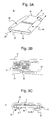
- FIGS 2A and 2B illustrate modules 1a and 1b, respectively, in which the carrier film 13 contains conductive traces 15 printed on one side.
- the traces 15 electrically contact the active surface of cell 3a (i.e., the front electrode 7 of cell 3a) collecting current generated on that cell 3a.
- a conductive interstitial material may be added between the conductive trace 15 and the cell 3a to improve the conduction and/or to stabilize the interface to environmental or thermal stresses.
- the interconnection to the second cell 3b is completed by a conductive tab 25 which contacts both the conductive trace 15 and the back side of cell 3b (i.e., the back side electrode 9 of cell 3b).
- the tab 25 may be continuous across the width of the cells or may comprise intermittent tabs connected to matching conductors on the cells.
- the electrical connection can be made with conductive interstitial material, conductive adhesive, solder, or by forcing the tab material 25 into direct intimate contact with the cell or conductive trace. Embossing the tab material 25 may improve the connection at this interface.
- the collector-connector 11 extends over the back side of the cell 3b and the tab 25 is located over the back side of cell 3b to make an electrical contact between the trace 15 and the back side electrode of cell 3b.
- the collector-connector 11 is located over the front side of the cell 3a and the tab 25 extends from the front side of cell 3a to the back side of cell 3b to electrically connect the trace 15 to the back side electrode of cell 3b.
- the conductor 15 is located on one side of the carrier film 13. At least a first part 13a of carrier 13 is located over a front surface of the first photovoltaic cell 3a such that the conductor 15 electrically contacts the first polarity electrode 7 on the front side of the first photovoltaic cell 3a to collect current from cell 3a.
- An electrically conductive tab 25 electrically connects the conductor 15 to the second polarity electrode 9 of the second photovoltaic cell 3b.
- a second part 13b of carrier 13 extends between the first photovoltaic cell 3a and the second photovoltaic cell 3b, such that an opposite side of the carrier 13 from the side containing the conductor 15 contacts a back side of the second photovoltaic cell 3b.
- FIGs 3A-3C illustrate module 1c having another configuration.
- the carrier film 13 contains the conductive traces 15 printed on one side of the film 13.
- the film 13 is applied such that the traces 15 contact the active surface of cell 3a collecting current generated on that cell 3a.
- the interconnection to the next cell 3b is completed by folding the carrier film 13 as shown in Figures 3A and 3C, at the dashed lines 23 shown in Figure 3B.
- the large busbars 35 on the side of the carrier film 13 contact the back side (i.e., the back side electrode) of the next cell 3b in the string forming the interconnection.
- module 1c While two cells are shown in the Figures 3A-3C, more than two cells may be incorporated into module 1c, with the carrier film 13 being folded over the cells lined up side by side. It should be noted that the module 1c is shown upside down in Figure 3A to illustrate the fold, and the front, Sun facing side of the module 1c faces down in Figure 3A.
- the carrier 13 comprises a sheet comprising a first part 33 which extends over front sides of the first and the second photovoltaic cells 3a, 3b, and a second part 43 which is folded over back sides of the first and the second photovoltaic cells.
- the conductor 15 includes a plurality of buses 35 which extend from the first part 33 of the carrier 33 to the second part 43 of the carrier 13 to electrically connect the first polarity electrode on the front side of the first photovoltaic cell to the second polarity electrode on the back side of the second photovoltaic cell.
- FIGs 4A-4C illustrate module 1d having another configuration.
- the carrier film 13 contains conductive traces 15 printed on one side.
- the collector-conductor 11 is applied such that the traces 15 contact the active surface 7 of cell 3a collecting current generated on that cell, as shown in Figures 4B and 4C.
- the interconnection to the next cell 3b is completed by folding the collector-connector (i.e., the carrier film 13 and conductive trace 15 assembly) on itself at the dashed line 33 such that the extensions of the busbar traces past the fold 34 make contact to the back side 9 of the next cell 3b in the string forming the interconnection.
- the conductor 15 is located on one side of the carrier 13.
- the carrier 13 is folded over such that an opposite side of the carrier is on an inside of a fold (i.e., such that the adhesive is located between two portions of the folded carrier 13).
- the conductor 15 electrically connects the first polarity electrode 7 on the front side of the first photovoltaic cell 3a to the second polarity electrode 9 on the back side of the second photovoltaic cell 3b.
- Figures 5A-5C illustrate module le having another configuration.
- the carrier film 13 also has the conductive traces 15 printed on one side, and the traces contact the active surface 7 of cell 3a collecting current generated on that cell.
- the interconnection to the next cell 3b is completed by piercing tabs 53 in the carrier film 13 and folding the tabs (with conductive trace 15 connected to the busbars 35) back against the underside (i.e., back side 9) of the adjacent cell 3b, thus making electrical contact between the trace 15 and the back side of the cell 3b.
- the conductive trace 15 on the tab 53 can be formed in such a way that it is printed with an insulating material in the region 54 to prevent possible shunting against the edge of the cell, and can be embossed in the region 55 (i.e., where the openings made by the removed tabs 53 in the film 13 are located) to improve electrical contact with the back side of the cell 3b.
- the conductive traces can be printed as shown in Figure 5C such that all of the required busbars and interconnects 36 for an entire module are printed on one side of the carrier film 13. The interconnect is made as discussed above with tabs 53.
- the traces 36 could plug directly into the junction box or other connector on the outside of the module 1e.
- the carrier 13 comprises a sheet comprising a plurality of tabs 53 extending out of a first side 13a of the sheet.
- the conductor 15 has a first part 15a which is located on the first side 13a of the sheet 13 and a second part 15b which is located on the side of the first tab 53a facing the first side 13a of the sheet 13 when in the folded-over position.
- the first photovoltaic cell 3a is located between the first side 13a of the sheet 13 and the first side of the first tab 53a.
- the second photovoltaic cell 3b is located between the first side 13a of the sheet 13 and a first side of a second tab 53b.
- the first part 15a of the conductor 15 electrically contacts the first polarity electrode 7 on the front side of the first photovoltaic cell 3a.
- the second part 15b of the conductor 15 electrically contacts the second polarity electrode 9 on the back side of the second photovoltaic cell 3b.
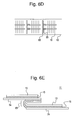
- FIGS 6A-6E illustrate module 1f having another configuration.
- full strings of interconnected cells can be fabricated by cutting slots (i.e., slits or other shaped openings) 63 into the carrier film 13 that allow the end of the cells 3 to pass through the slot 63.
- the cell 3a extends through the slot 63 with a part of the cell located above the carrier 13 and another part located below the carrier 13.
- the front and back side electrodes 7, 9 make electrical contact to the conductive traces 15a, 15b on upper and lower sides of the carrier 13.
- the electrical connection can be configured as shown in Figures 6A-6C, where the traces 15a, 15b are printed on both sides of the carrier film 13.
- the traces 15a and 15b are electrically contiguous from front to back of the carrier film 13 in region 64 (i.e., the conductor extends through the carrier 13 or around the edge of the carrier to connect traces 15a and 15b).
- the back side of the portion of the cell 3b that is inserted in the slot 63 makes contact with trace 15b there only.
- the interconnection can be made by using tabs 65, as shown in Figures 6D-6E.
- the traces 15 are printed on just one side of the carrier film 13.
- the tabs 65 located adjacent to the slots 63 in the carrier film can be folded back in the tab region such that contact is made between the front side of cell 3b collecting current generated on that cell and the back side of cell 3a, by the conductive trace 15 as the cells are inserted in the respective slots.
- the carrier 13 comprises a sheet containing a plurality of slots 63.
- the conductor 15 has a first part 15a located on a first side of the sheet 13 between a first slot 63a and a second slot 63b, and a second part 15b located on a second side of the sheet between the first slot and the second slot.
- the first photovoltaic cell 3a passes through the first slot 63a such that the first polarity electrode 7 on the front side of the first photovoltaic cell 3a electrically contacts the first part 15a of the conductor 15.
- the second photovoltaic cell 3b passes through the second slot 63b such that the second polarity electrode 9 on the back side of the second photovoltaic cell electrically contacts the second part 15b of the conductor 15.
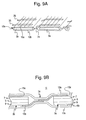
- Figures 7A-7D illustrate module lg having another configuration.
- the first and the second photovoltaic cells 3a, 3b comprise lateral type cells having electrodes 7, 9 of both polarities exposed on a same side of each cell.
- both electrodes 7, 9 are exposed in the front surface of the cells.
- the interconnection to the back contact 9 on the cells 3 can be made by selectively removing small regions of the photovoltaic film 5 from the front surface of the cells 3 thus exposing the back contact 9 in those regions.
- the carrier film 13 can have the conductive traces 15 printed on one side, and be applied such that the traces 15 contact the active surface (i.e., the front electrode 7) of cell 3a collecting current generated on that cell.
- the interconnection to the next cell 3b can be completed by extending the traces to the regions on the adjacent cells where the back contact 9 has been exposed. This can be done by connecting a bus portion 35 of the conductor 15 to a lip 9 on the front edge of the adjacent cell as shown in Figure 7B, to one or both sides of the adjacent cell as shown in Figure 7C or to alternate sides of adjacent cells as shown in Figure 7D.
- the carrier 13 may be in the shape of ribbon or sheet which is unrolled from a spool or roll.
- the first and the second photovoltaic cells 3a, 3b comprise lateral type cells having electrodes 7, 9 of both polarities exposed on a same side of each cell.
- the conductor 15, 35 is located on one side of the carrier 13.
- the conductor 15, 35 electrically connects the second polarity electrode 9 of the second photovoltaic cell 3b to the first polarity electrode 7 of the first photovoltaic cell 3a as shown in Figures 7B-7D.
- Figures 8A-8B illustrate module 1h having another configuration.
- the conductive trace 15 is formed on both sides of the carrier film 13.
- the conductive trace 15 is connected contiguously in selected regions to make contact to the front of one cell 3a and the back of adjacent cell 3b without folding, cutting, or twisting the carrier film 13. This can be done as shown in Figure 8A, where the trace 15 changes sides of the carrier film 13 underneath the adjacent cell 3b in region 74, or as shown in Figure 8B, where the trace switches sides on top of the cell 3a in region 76.
- the configuration in Figure 8B has the advantage of avoiding a possible shunt path at the edge of the cell.
- the region 74 or 76 may be located between the cells 3a, 3b, if desired.
- the conductive material 15 can be transferred to the opposite side of the cell by way of via holes, perforations made by laser or stamping techniques, or if the region 74, 76 of the carrier film 13 is permeable to the material that comprises the conductive trace, then the trace is permeated through the carrier film 13. In other words, the trace is switched from one side of the carrier film to the other side through a hole or a permeable region in the carrier 13.
- the conductor has a first part 15a which is located on one side of the carrier 13 and a second part 15b which is located on the opposite side of the carrier.
- One part of the carrier is located over a front surface of the first photovoltaic cell 3a such that the first part 15a of the conductor 15 electrically contacts the first polarity electrode 7 on a front side of the first photovoltaic cell 3a.
- Another part of carrier 13 extends between the first photovoltaic cell 3a and the second photovoltaic cell 3b and over a back side of the second photovoltaic cell 3b, such that the second part 15b of the conductor 15 electrically contacts the second polarity electrode 9 on a back side of the second photovoltaic cell 3b.
- the module 1h is illustrated with two cells, it should be understood that the module may have more than two cells with the carrier film being shaped as a sheet or ribbon which is unrolled from a spool or roll and then cut into portions or decals which connect two cells.
- FIGS 9A-9B illustrate module 1i having another configuration.
- the module contains two sheets or ribbons of carrier film 13a, 13b.
- Each carrier 13a, 13b is selectively printed with conductive traces (and/or supports wires) 15 that contact the front and back of each cell 3a, 3b such that the traces 15a that contact the front (i.e., the front electrode 7) of cell 3a collecting current generated on that cell, and the traces 15b that contact the back of cell 3b, make contact with each other in the region 74, as shown in Figure 9B.
- the connection in region 74 connects the traces 15a, 15b both electrically and mechanically.
- connection methods include direct physical contact (i.e., pressing the traces together), solder (such as SnBi or SnPb), conductive adhesive, embossing, mechanical connection means, solvent bonding or ultrasonic bonding.
- solder such as SnBi or SnPb
- conductive adhesive such as SnBi or SnPb
- embossing such as embossing
- mechanical connection means such as solvent bonding or ultrasonic bonding.
- the module 1i includes a collector-connector 11 which comprises a first flexible sheet or ribbon shaped, electrically insulating carrier 13a supporting a first conductor 15a, and a second flexible sheet or ribbon shaped, electrically insulating carrier 13b supporting a second conductor 15b.
- the first conductor 15a electrically contacts a major portion of a surface of the first polarity electrode 7 of the first photovoltaic cell 3a.
- the second conductor 15b electrically contacts the first conductor 15a and at least a portion of the second polarity electrode 9 of the second photovoltaic cell 3b.
- the first carrier 13a comprises a passivation material of the module 1i and the second carrier 13b comprises a back support material of the module.
- the top carrier film 13a is the upper layer of the module which acts as the passivation and protection film of the module.
- the bottom carrier film 13b is the back support film which supports the module over the installation location support, such as a roof of a building, vehicle roof (including wings of plane or tops of blimps) or other structure or a solar cell stand or platform (i.e., for free standing photovoltaic modules supported on a dedicated stand or platform).
- the bottom carrier film may also support auxiliary electronics for connection to junction boxes.
- the carriers 13 may comprise any suitable polymer materials
- the first carrier 13a comprises a thermal plastic olefin (TPO) sheet
- the second carrier 13b comprises a second thermal plastic olefin membrane roofing material sheet which is adapted to be mounted over a roof support structure.
- the photovoltaic module 1j shown in Figure 10 includes only three elements: the first thermal plastic olefin sheet 13a supporting the upper conductors 15a on its inner surface, a second thermal plastic olefin sheet 13b supporting the lower conductors 15b on its inner surface, and a plurality photovoltaic cells 3 located between the two thermal plastic olefin sheets 13a, 13b.
- the electrical conductors 15a, 15b electrically interconnect the plurality of photovoltaic cells 3 in the module, as shown in Figure 10.
- this module 1j is a building integrated photovoltaic (BIPV) module which can be used instead of a roof in a building (as opposed to being installed on a roof) as shown in Figure 10.
- the outer surface of the second thermal plastic olefin sheet 13b is attached to a roof support structure of a building, such as plywood or insulated roofing deck.
- the module 1j comprises a building integrated module which forms at least a portion of a roof of the building.
- an adhesive is provided on the back of the solar module 1j (i.e., on the outer surface of the bottom carrier sheet 13b) and the module is adhered directly to the roof support structure, such as plywood or insulated roofing deck.
- the module 1j can be adhered to the roof support structure with mechanical fasteners, such as clamps, bolts, staples, nails, etc.
- mechanical fasteners such as clamps, bolts, staples, nails, etc.
- most of the wiring can be integrated into the TPO back sheet 13b busbar print, resulting in a large area module with simplified wiring and installation.
- the module is simply installed in lieu of normal roofing, greatly reducing installation costs and installer markup on the labor and materials.
- FIG 10 illustrates two modules 1j installed on a roof or a roofing deck 85 of a residential building, such as a single family house or a townhouse.
- Each module 1j contains output leads 82 extending from a junction box 84 located on or adjacent to the back sheet 13b.
- the leads 82 can be simply plugged into existing building wiring 81, such as an inverter, using a simple plug-socket connection 83 or other simple electrical connection, as shown in a cut-away view in Figure 10.
- the junction box 84 may be located in the portion of the module 1j (such as the upper portion shown in Figure 10) which is located over the attic 86 to allow the electrical connection 83 to be made in an accessible attic, to allow an electrician or other service person or installer to install and/or service the junction box and the connection by coming up to the attic rather than by removing a portion of the module or the roof.
- the module 1j may comprise a flexible module in which the first thermal plastic olefin sheet 13a comprises a flexible top sheet of the module having an inner surface and an outer surface.
- the second thermal plastic olefin sheet 13b comprises a back sheet of the module having an inner surface and an outer surface.
- the plurality of photovoltaic cells 3 comprise a plurality of flexible photovoltaic cells located between the inner surface of the first thermal plastic olefin sheet 13a and the inner surface of the second thermal plastic olefin sheet 13b.
- the cells 3 may comprise CIGS type cells formed on flexible substrates comprising a conductive foil.
- the electrical conductors include flexible wires or traces 15a located on and supported by the inner surface of the first thermal plastic olefin sheet 13a, and a flexible wires or traces 15b located on and supported by the inner surface of the second thermal plastic olefin sheet 13b.
- the conductors 15 are adapted to collect current from the plurality of photovoltaic cells 3 during operation of the module and to interconnect the cells.
- TPO is described as one exemplary carrier 13 material
- one or both carriers 13a, 13b may be made of other insulating polymer or non-polymer materials, such as EVA and/or PET for example, or other polymers which can form a membrane roofing material.
- the top carrier 13a may comprise an acrylic material while the back carrier 13b may comprise PVC or asphalt material.
- the carriers 13 may be formed by extruding the resins to form single ply (or multi-ply if desired) membrane roofing and then rolled up into a roll.
- the grid lines 15 and busbars 35 are then printed on large rolls of clear TPO or other material which would form the top sheet of the solar module 1j.
- TPO could replace the need for EVA while doubling as a replacement for glass.
- a second sheet 13b of regular membrane roofing would be used as the back sheet, and can be a black or a white sheet for example.
- the second sheet 13b may be made of TPO or other roofing materials.
- the cells 3 are laminated between the two layers 13a, 13b of pre-printed polymer material, such as TPO.
- the top TPO sheet 13a can replace both glass and EVA top laminate of the prior art rigid modules, or it can replace the Tefzel/EVA encapsulation of the prior art flexible modules.
- the bottom TPO sheet 13b can replace the prior art EVA/Tedlar bottom laminate.
- the module 1j architecture would consist of TPO sheet 13a, conductor 15a, cells 3, conductor 15b and TPO sheet 13b, greatly reducing material costs and module assembly complexity.
- the modules lj can be made quite large in size and their installation is simplified. If desired, one or more luminescent dyes which convert shorter wavelength (i.e., blue or violet) portions of sunlight to longer wavelength (i.e., orange or red) light may be incorporated into the top TPO sheet 13a.
- the module 1k can contain PV cells 3 which are shaped as shingles to provide a conventional roofing material appearance, such as an asphalt shingle appearance, for a commercial or a residential building.
- a conventional roofing material appearance such as an asphalt shingle appearance
- This may be advantageous for buildings such as residential single family homes and townhouses located in communities that require a conventional roofing material appearance, such as in communities that contain a neighborhood association with an architectural control committee and/or strict house appearance covenants or regulations, or for commercial or residential buildings in historic preservation areas where the building codes or other similar type regulations require the roof to have a shingle type appearance.
- the cells 3 may be located in stepped rows on the back sheet 13b, as shown in Figure 11 (the optically transparent front sheet 13a is not shown for clarity) to give an appearance that the roof is covered with shingles.
- the back sheet 13b may have a stepped surface facing the cells 3.
- the cells in each row may partially overlap over the cells in the next lower row or the cells in adjacent rows may avoid overlapping as shown in Figure 11 to increase the available light receiving area of each cell.
- the layered look of shingles could be achieved in the factory along with greatly simplified in the field wiring requirements to lower module and installation costs.
- FIG 12A illustrates the side cross sectional view of a PV cell 3 according to another embodiment of the invention.
- This cell 3 may be used as a "drop-in" replacement for a non-functioning or malfunctioning cell in a module.
- the cell 3 may be included in an original module (i.e., in a new or originally constructed module).
- the cell 3 contains a carrier 13 with conductor portions 15a and 15b located on inner and outer surfaces of the carrier 13, respectively.
- the conductor portions 15a and 15b may be printed and/or plated on both sides of the carrier 13 and connected to each other through hole(s) or via(s) (not shown in Figure 12A for clarity) in the carrier.
- the conductor portion 15a on the inner side of the carrier 13 may comprise both thick buslines 35 and thin grid lines 15 which are used to collect current from the cell 3.
- the buslines 35 on the inner side of the carrier are electrically connected to the buslines 35 which make up the conductor portion 15b on the outer side of the carrier 13.
- the conductor portion 15b can be electrically connected to the next cell in the module using the conventional tab and string interconnect or other suitable interconnects.
- the conductor portion 15a is located on a inner side of insulating carrier 13 and facing the front side electrode 7 of the cell 3, such that the conductor portion 15a contacts the front side electrode 7 to collect current from the front side electrode.
- the other conductor portion 15b is located on an outer side of the insulating carrier 13 and is electrically connected to the first conductor portion 15a.
- An interconnect such as a tab and string or other interconnect can be electrically connected to the conductor portion 15b to electrically connect the front electrode 7 of the cell 3 to a back side electrode of another photovoltaic cell in a module.
- the cell 3 can be used in any type of module, such as a module in which the cells are interconnected using the conventional tab and string interconnects.
- the cell 3 may contain any suitable photovoltaic material 5 described above.
- a cell 3 with a CIGS photovoltaic material 5 may be used as a replacement for another CIGS PV material containing cell, while a cell with a silicon photovoltaic material 5 may be used as a replacement for another silicon PV material containing cell.
- Figures 13 and 14 are photographs of flexible CIGS PV cells formed on flexible stainless steel substrates.
- the collector-connector containing a flexible insulating carrier and conductive traces shown in Figure 2a and described above is formed over the top of the cells.
- the carrier comprises a PET/EVA co-extrusion and the conductor comprises electrolessly plated copper traces.
- Figure 14 illustrates the flexible nature of the cell, which is being lifted and bent by hand.
- Table I shows the electrical characteristics of three cells according to the specific embodiments of the invention.
- Table I Cell No. V oc I sc V pmax I pmax FF Power (mW) Efficiency 1 413 3.7 255 2.64 0.44 673.2 2.99 2 398 4.13 237 2.74 0.40 649.4 2.89 3 412 4.15 250 2.88 0.42 720.0 3.20
Abstract
Description
- The present invention relates generally to a photovoltaic device and more particularly to photovoltaic modules having an integrated current collection and interconnection configuration.
- Many current collection methods in photovoltaic ("PV") devices (which are also known as solar cell devices) use conductive inks that are screen printed on the surface of the PV cell. Alternative current collection methods involve conductive wires that are placed in contact with the cell.
- A large portion of prior art PV cells are interconnected by using the so-called "tab and string" technique of soldering two or three conductive ribbons between the front and back surfaces of adjacent cells. Alternative interconnect configurations include shingled interconnects with conductive adhesives. Some prior art PV devices also include embossing of an adhesive backed metal foil to enhance conductivity of the substrate of the device.
- However, the "tab and string" interconnection configuration suffers from poor yield and reliability due to solder joints that fail from thermal coefficient of expansion mismatches and defects, requires significant labor or capital equipment to assemble, and does not pack the cells in a PV module very closely. In addition, previous attempts at shingled interconnects have been plagued by reliability problems from degradation of the conductive adhesives used.
- One embodiment of the invention includes a photovoltaic module comprising a first photovoltaic cell, a second photovoltaic cell, and a collector-connector which is configured to collect current from the first photovoltaic cell and to electrically connect the first photovoltaic cell with the second photovoltaic cell.
- Another embodiment of the invention includes a photovoltaic module comprising a first photovoltaic cell, a second photovoltaic cell, and an interconnect comprising an electrically insulating carrier and at least one electrical conductor which electrically connects the first photovoltaic cell to the second photovoltaic cell.
- Another embodiment of the invention includes a photovoltaic module comprising a first thermal plastic olefin sheet, a second flexible membrane roofing sheet, a plurality photovoltaic cells located between the first and the second sheets, and a plurality of electrical conductors which electrically interconnect the plurality of photovoltaic cells.
- Figures 1-12B are schematic illustrations of the components of photovoltaic modules of the embodiments of the invention. Figures 1, 2A, 2B, 3C, 4B, 4C, 5B, 6C, 6E, 9B, 8A, 8B, 10, 11 and 12A are side cross sectional views. Figures 3A, 5A, 7A and 9A are three dimensional views. Figures 3B, 4A, 5C, 6A, 6B, 6D, 7B-7D and 12B are top views. The dimensions of the components in the Figures are not necessarily to scale.
- Figures 13 and 14 are photographs of photovoltaic cells according to the examples of the invention.
- One embodiment of the invention provides a photovoltaic module including at least two photovoltaic cells and a collector-connector. As used herein, the term "module" includes an assembly of at least two, and preferably three or more electrically interconnected photovoltaic cells, which may also be referred to as "solar cells". The "collector-connector" is a device that acts as both a current collector to collect current from at least one photovoltaic cell of the module, and as an interconnect which electrically interconnects the at least one photovoltaic cell with at least one other photovoltaic cell of the module. In general, the collector-connector takes the current collected from each cell of the module and combines it to provide a useful current and voltage at the output connectors of the module.
- Another embodiment of the invention provides a photovoltaic module which includes an interconnect comprising an electrically insulating carrier and at least one electrical conductor which electrically connects one photovoltaic cell to at least one other photovoltaic cell of the module. Preferably, but not necessarily, this interconnect comprises the collector-connector which acts as both a current collector to collect current from at least one photovoltaic cell of the module and as an interconnect which electrically interconnects the at least one photovoltaic cell with at least one other photovoltaic cell of the module.
- Figure 1 schematically illustrates a
module 1 of the first and second embodiments of the invention. Themodule 1 includes first and secondphotovoltaic cells module 1 may contain three or more cells, such as 3-10,000 cells for example. Preferably, the first 3a and the second 3b photovoltaic cells are plate shaped cells which are located adjacent to each other, as shown schematically in Figure 1. The cells may have a square, rectangular (including ribbon shape), hexagonal or other polygonal, circular, oval or irregular shape when viewed from the top. - Each
cell photovoltaic material 5, such as a semiconductor material. For example, the photovoltaic semiconductor material may comprise a p-n or p-i-n junction in a Group IV semiconductor material, such as amorphous or crystalline silicon, a Group II-VI semiconductor material, such as CdTe or CdS, a Group I-III-VI semiconductor material, such as CuInSe2 (CIS) or Cu(In,Ga)Se2 (CIGS), and/or a Group III-V semiconductor material, such as GaAs or InGaP. The p-n junctions may comprise heterojunctions of different materials, such as CIGS/CdS heterojunction, for example. Eachcell back side electrodes electrodes front side electrode 7 may be electrically connected to an n-side of a p-n junction and the back side electrode may be electrically connected to a p-side of a p-n junction. Theelectrode 7 on the front surface of the cells may be an optically transparent front side electrode which is adapted to face the Sun, and may comprise a transparent conductive material such as indium tin oxide or aluminum doped zinc oxide. Theelectrode 9 on the back surface of the cells may be a back side electrode which is adapted to face away from the Sun, and may comprise one or more conductive materials such as copper, molybdenum, aluminum, stainless steel and/or alloys thereof. Thiselectrode 9 may also comprise the substrate upon which thephotovoltaic material 5 and thefront electrode 7 are deposited during fabrication of the cells. - The module also contains the collector-
connector 11, which comprises an electricallyinsulating carrier 13 and at least oneelectrical conductor 15. The collector-connector 11 electrically contacts thefirst polarity electrode 7 of the firstphotovoltaic cell 3a in such a way as to collect current from the first photovoltaic cell. For example, theelectrical conductor 15 electrically contacts a major portion of a surface of thefirst polarity electrode 7 of the firstphotovoltaic cell 3a to collect current fromcell 3a. Theconductor 15 portion of the collector-connector 11 also electrically contacts thesecond polarity electrode 9 of the secondphotovoltaic cell 3b to electrically connect thefirst polarity electrode 7 of the firstphotovoltaic cell 3a to thesecond polarity electrode 9 of the secondphotovoltaic cell 3b. - Preferably, the
carrier 13 comprises a flexible, electrically insulating polymer film having a sheet or ribbon shape, supporting at least oneelectrical conductor 15. Examples of suitable polymer materials include thermal polymer olefin (TPO). TPO includes any olefins which have thermoplastic properties, such as polyethylene, polypropylene, polybutylene, etc. Other polymer materials which are not significantly degraded by sunlight, such as EVA, other non-olefin thermoplastic polymers, such as fluoropolymers, acrylics or silicones, as well as multilayer laminates and co-extrusions, such as PET/EVA laminates or co-extrusions, may also be used. Theinsulating carrier 13 may also comprise any other electrically insulating material, such as glass or ceramic materials. Thecarrier 13 may be a sheet or ribbon which is unrolled from a roll or spool and which is used to support conductor(s) 15 which interconnect three ormore cells 3 in amodule 1. Thecarrier 13 may also have other suitable shapes besides sheet or ribbon shape. - The
conductor 15 may comprise any electrically conductive trace or wire. Preferably, theconductor 15 is applied to aninsulating carrier 13 which acts as a substrate during deposition of the conductor. The collector-connector 11 is then applied in contact with thecells 3 such that theconductor 15 contacts one ormore electrodes cells 3. For example, theconductor 15 may comprise a trace, such as silver paste, for example a polymer-silver powder mixture paste, which is spread, such as screen printed, onto thecarrier 13 to form a plurality of conductive traces on thecarrier 13. Theconductor 15 may also comprise a multilayer trace. For example, the multilayer trace may comprise a seed layer and a plated layer. The seed layer may comprise any conductive material, such as a silver filled ink or a carbon filled ink which is printed on thecarrier 13 in a desired pattern. The seed layer may be formed by high speed printing, such as rotary screen printing, flat bed printing, rotary gravure printing, etc. The plated layer may comprise any conductive material which can by formed by plating, such as copper, nickel, cobalt or their alloys. The plated layer may be formed by electroplating by selectively forming the plated layer on the seed layer which is used as one of the electrodes in a plating bath. Alternatively, the plated layer may be formed by electroless plating. Alternatively, theconductor 15 may comprise a plurality of metal wires, such as copper, aluminum, and/or their alloy wires, which are supported by or attached to thecarrier 13. The wires or thetraces 15 electrically contact a major portion of a surface of thefirst polarity electrode 7 of the firstphotovoltaic cell 3a to collect current from thiscell 3a. The wires or thetraces 15 also electrically contact at least a portion of thesecond polarity electrode 9 of the secondphotovoltaic cell 3b to electrically connect thiselectrode 9 ofcell 3b to thefirst polarity electrode 7 of the firstphotovoltaic cell 3a. The wires or traces 15 may form a grid-like contact to theelectrode 7. The wires or traces 15 may include thin gridlines as well as optional thick busbars or buslines, as will be described in more detail below. If busbars or buslines are present, then the gridlines may be arranged as thin "fingers" which extend from the busbars or buslines. - The modules of the embodiments of the invention provide a current collection and interconnection configuration and method that is less expensive, more durable, and allows more light to strike the active area of the photovoltaic module than the prior art modules. The module provides collection of current from a photovoltaic ("PV") cell and the electrical interconnection of two or more PV cells for the purpose of transferring the current generated in one PV cell to adjacent cells and/or out of the photovoltaic module to the output connectors. In addition, the carrier is may be easily cut, formed, and manipulated. In addition, when interconnecting thin- film solar cells with a metallic substrate, such as stainless steel, the embodiments of the invention allow for a better thermal expansion coefficient match between the interconnecting solders used and the solar cell than with traditional solder joints on silicon PV cells) In particular, the cells of the module may be interconnected without using soldered tab and string interconnection techniques of the prior art. However, soldering may be used if desired.
- Figures 2A to 11 illustrate exemplary, non-limiting configurations of the modules of the embodiments of the invention.
- Figures 2A and 2B illustrate
modules carrier film 13 contains conductive traces 15 printed on one side. Thetraces 15 electrically contact the active surface ofcell 3a (i.e., thefront electrode 7 ofcell 3a) collecting current generated on thatcell 3a. A conductive interstitial material may be added between theconductive trace 15 and thecell 3a to improve the conduction and/or to stabilize the interface to environmental or thermal stresses. The interconnection to thesecond cell 3b is completed by aconductive tab 25 which contacts both theconductive trace 15 and the back side ofcell 3b (i.e., theback side electrode 9 ofcell 3b). Thetab 25 may be continuous across the width of the cells or may comprise intermittent tabs connected to matching conductors on the cells. The electrical connection can be made with conductive interstitial material, conductive adhesive, solder, or by forcing thetab material 25 into direct intimate contact with the cell or conductive trace. Embossing thetab material 25 may improve the connection at this interface. In the configuration shown in Figure 2A, the collector-connector 11 extends over the back side of thecell 3b and thetab 25 is located over the back side ofcell 3b to make an electrical contact between thetrace 15 and the back side electrode ofcell 3b. In the configuration of Figure 2B, the collector-connector 11 is located over the front side of thecell 3a and thetab 25 extends from the front side ofcell 3a to the back side ofcell 3b to electrically connect thetrace 15 to the back side electrode ofcell 3b. - In summary, in the module configuration of Figures 2A and 2B, the
conductor 15 is located on one side of thecarrier film 13. At least afirst part 13a ofcarrier 13 is located over a front surface of the firstphotovoltaic cell 3a such that theconductor 15 electrically contacts thefirst polarity electrode 7 on the front side of the firstphotovoltaic cell 3a to collect current fromcell 3a. An electricallyconductive tab 25 electrically connects theconductor 15 to thesecond polarity electrode 9 of the secondphotovoltaic cell 3b. Furthermore, in themodule 1a of Figure 2A, asecond part 13b ofcarrier 13 extends between the firstphotovoltaic cell 3a and the secondphotovoltaic cell 3b, such that an opposite side of thecarrier 13 from the side containing theconductor 15 contacts a back side of the secondphotovoltaic cell 3b. - Figures 3A-3C illustrate
module 1c having another configuration. As shown in Figure 3B, thecarrier film 13 contains the conductive traces 15 printed on one side of thefilm 13. Thefilm 13 is applied such that thetraces 15 contact the active surface ofcell 3a collecting current generated on thatcell 3a. The interconnection to thenext cell 3b is completed by folding thecarrier film 13 as shown in Figures 3A and 3C, at the dashedlines 23 shown in Figure 3B. Thelarge busbars 35 on the side of thecarrier film 13 contact the back side (i.e., the back side electrode) of thenext cell 3b in the string forming the interconnection. While two cells are shown in the Figures 3A-3C, more than two cells may be incorporated intomodule 1c, with thecarrier film 13 being folded over the cells lined up side by side. It should be noted that themodule 1c is shown upside down in Figure 3A to illustrate the fold, and the front, Sun facing side of themodule 1c faces down in Figure 3A. - In summary, in the
module 1c shown in Figures 3A-3C, thecarrier 13 comprises a sheet comprising afirst part 33 which extends over front sides of the first and the secondphotovoltaic cells second part 43 which is folded over back sides of the first and the second photovoltaic cells. Theconductor 15 includes a plurality ofbuses 35 which extend from thefirst part 33 of thecarrier 33 to thesecond part 43 of thecarrier 13 to electrically connect the first polarity electrode on the front side of the first photovoltaic cell to the second polarity electrode on the back side of the second photovoltaic cell. - Figures 4A-4C illustrate
module 1d having another configuration. Inmodule 1d, thecarrier film 13 contains conductive traces 15 printed on one side. The collector-conductor 11 is applied such that thetraces 15 contact theactive surface 7 ofcell 3a collecting current generated on that cell, as shown in Figures 4B and 4C. The interconnection to thenext cell 3b is completed by folding the collector-connector (i.e., thecarrier film 13 andconductive trace 15 assembly) on itself at the dashedline 33 such that the extensions of the busbar traces past thefold 34 make contact to theback side 9 of thenext cell 3b in the string forming the interconnection. This can be done in a shingled configuration where thecells cells - In summary, in
module 1d, theconductor 15 is located on one side of thecarrier 13. Thecarrier 13 is folded over such that an opposite side of the carrier is on an inside of a fold (i.e., such that the adhesive is located between two portions of the folded carrier 13). Theconductor 15 electrically connects thefirst polarity electrode 7 on the front side of the firstphotovoltaic cell 3a to thesecond polarity electrode 9 on the back side of the secondphotovoltaic cell 3b. - Figures 5A-5C illustrate module le having another configuration. In this configuration, the
carrier film 13 also has the conductive traces 15 printed on one side, and the traces contact theactive surface 7 ofcell 3a collecting current generated on that cell. The interconnection to thenext cell 3b is completed by piercingtabs 53 in thecarrier film 13 and folding the tabs (withconductive trace 15 connected to the busbars 35) back against the underside (i.e., back side 9) of theadjacent cell 3b, thus making electrical contact between thetrace 15 and the back side of thecell 3b. - The
conductive trace 15 on thetab 53 can be formed in such a way that it is printed with an insulating material in theregion 54 to prevent possible shunting against the edge of the cell, and can be embossed in the region 55 (i.e., where the openings made by the removedtabs 53 in thefilm 13 are located) to improve electrical contact with the back side of thecell 3b. In addition, the conductive traces can be printed as shown in Figure 5C such that all of the required busbars and interconnects 36 for an entire module are printed on one side of thecarrier film 13. The interconnect is made as discussed above withtabs 53. Thetraces 36 could plug directly into the junction box or other connector on the outside of themodule 1e. - In summary, in
module 1e, thecarrier 13 comprises a sheet comprising a plurality oftabs 53 extending out of afirst side 13a of the sheet. Theconductor 15 has afirst part 15a which is located on thefirst side 13a of thesheet 13 and asecond part 15b which is located on the side of thefirst tab 53a facing thefirst side 13a of thesheet 13 when in the folded-over position. The firstphotovoltaic cell 3a is located between thefirst side 13a of thesheet 13 and the first side of thefirst tab 53a. The secondphotovoltaic cell 3b is located between thefirst side 13a of thesheet 13 and a first side of asecond tab 53b. Thefirst part 15a of theconductor 15 electrically contacts thefirst polarity electrode 7 on the front side of the firstphotovoltaic cell 3a. Thesecond part 15b of theconductor 15 electrically contacts thesecond polarity electrode 9 on the back side of the secondphotovoltaic cell 3b. - Figures 6A-6E illustrate
module 1f having another configuration. In this configuration, full strings of interconnected cells (or modules for that matter) can be fabricated by cutting slots (i.e., slits or other shaped openings) 63 into thecarrier film 13 that allow the end of thecells 3 to pass through theslot 63. As shown in Figures 6B and 6C, thecell 3a extends through theslot 63 with a part of the cell located above thecarrier 13 and another part located below thecarrier 13. The front and backside electrodes conductive traces carrier 13. - The electrical connection can be configured as shown in Figures 6A-6C, where the
traces carrier film 13. Thetraces carrier film 13 in region 64 (i.e., the conductor extends through thecarrier 13 or around the edge of the carrier to connecttraces cell 3b that is inserted in theslot 63 makes contact withtrace 15b there only. - Alternatively, the interconnection can be made by using
tabs 65, as shown in Figures 6D-6E. In this configuration, thetraces 15 are printed on just one side of thecarrier film 13. Thetabs 65 located adjacent to theslots 63 in the carrier film can be folded back in the tab region such that contact is made between the front side ofcell 3b collecting current generated on that cell and the back side ofcell 3a, by theconductive trace 15 as the cells are inserted in the respective slots. - In summary, in the
module 1f, thecarrier 13 comprises a sheet containing a plurality ofslots 63. As shown in Figures 6B and 6C, theconductor 15 has afirst part 15a located on a first side of thesheet 13 between afirst slot 63a and asecond slot 63b, and asecond part 15b located on a second side of the sheet between the first slot and the second slot. The firstphotovoltaic cell 3a passes through thefirst slot 63a such that thefirst polarity electrode 7 on the front side of the firstphotovoltaic cell 3a electrically contacts thefirst part 15a of theconductor 15. The secondphotovoltaic cell 3b passes through thesecond slot 63b such that thesecond polarity electrode 9 on the back side of the second photovoltaic cell electrically contacts thesecond part 15b of theconductor 15. - Figures 7A-7D illustrate module lg having another configuration. In this configuration, the first and the second
photovoltaic cells cells having electrodes electrodes back contact 9 on thecells 3 can be made by selectively removing small regions of thephotovoltaic film 5 from the front surface of thecells 3 thus exposing theback contact 9 in those regions. - The
carrier film 13 can have the conductive traces 15 printed on one side, and be applied such that thetraces 15 contact the active surface (i.e., the front electrode 7) ofcell 3a collecting current generated on that cell. The interconnection to thenext cell 3b can be completed by extending the traces to the regions on the adjacent cells where theback contact 9 has been exposed. This can be done by connecting abus portion 35 of theconductor 15 to alip 9 on the front edge of the adjacent cell as shown in Figure 7B, to one or both sides of the adjacent cell as shown in Figure 7C or to alternate sides of adjacent cells as shown in Figure 7D. Thecarrier 13 may be in the shape of ribbon or sheet which is unrolled from a spool or roll. - In summary, in
module 1g, the first and the secondphotovoltaic cells cells having electrodes conductor carrier 13. Theconductor second polarity electrode 9 of the secondphotovoltaic cell 3b to thefirst polarity electrode 7 of the firstphotovoltaic cell 3a as shown in Figures 7B-7D. - Figures 8A-8B illustrate
module 1h having another configuration. In this configuration, theconductive trace 15 is formed on both sides of thecarrier film 13. Theconductive trace 15 is connected contiguously in selected regions to make contact to the front of onecell 3a and the back ofadjacent cell 3b without folding, cutting, or twisting thecarrier film 13. This can be done as shown in Figure 8A, where thetrace 15 changes sides of thecarrier film 13 underneath theadjacent cell 3b inregion 74, or as shown in Figure 8B, where the trace switches sides on top of thecell 3a inregion 76. The configuration in Figure 8B has the advantage of avoiding a possible shunt path at the edge of the cell. Theregion cells conductive material 15 can be transferred to the opposite side of the cell by way of via holes, perforations made by laser or stamping techniques, or if theregion carrier film 13 is permeable to the material that comprises the conductive trace, then the trace is permeated through thecarrier film 13. In other words, the trace is switched from one side of the carrier film to the other side through a hole or a permeable region in thecarrier 13. - In summary, in the
module 1h, the conductor has afirst part 15a which is located on one side of thecarrier 13 and asecond part 15b which is located on the opposite side of the carrier. One part of the carrier is located over a front surface of the firstphotovoltaic cell 3a such that thefirst part 15a of theconductor 15 electrically contacts thefirst polarity electrode 7 on a front side of the firstphotovoltaic cell 3a. Another part ofcarrier 13 extends between the firstphotovoltaic cell 3a and the secondphotovoltaic cell 3b and over a back side of the secondphotovoltaic cell 3b, such that thesecond part 15b of theconductor 15 electrically contacts thesecond polarity electrode 9 on a back side of the secondphotovoltaic cell 3b. While themodule 1h is illustrated with two cells, it should be understood that the module may have more than two cells with the carrier film being shaped as a sheet or ribbon which is unrolled from a spool or roll and then cut into portions or decals which connect two cells. - Figures 9A-9B illustrate
module 1i having another configuration. In this configuration, the module contains two sheets or ribbons ofcarrier film carrier cell traces 15a that contact the front (i.e., the front electrode 7) ofcell 3a collecting current generated on that cell, and thetraces 15b that contact the back ofcell 3b, make contact with each other in theregion 74, as shown in Figure 9B. The connection inregion 74 connects thetraces cells 3 may be covered with an insulating spacer to prevent thetraces 15 from short circuiting or shunting theopposite polarity electrodes - In summary, the
module 1i includes a collector-connector 11 which comprises a first flexible sheet or ribbon shaped, electrically insulatingcarrier 13a supporting afirst conductor 15a, and a second flexible sheet or ribbon shaped, electrically insulatingcarrier 13b supporting asecond conductor 15b. - The
first conductor 15a electrically contacts a major portion of a surface of thefirst polarity electrode 7 of the firstphotovoltaic cell 3a. Thesecond conductor 15b electrically contacts thefirst conductor 15a and at least a portion of thesecond polarity electrode 9 of the secondphotovoltaic cell 3b. - In another embodiment of the invention, the
first carrier 13a comprises a passivation material of themodule 1i and thesecond carrier 13b comprises a back support material of the module. In other words, thetop carrier film 13a is the upper layer of the module which acts as the passivation and protection film of the module. Thebottom carrier film 13b is the back support film which supports the module over the installation location support, such as a roof of a building, vehicle roof (including wings of plane or tops of blimps) or other structure or a solar cell stand or platform (i.e., for free standing photovoltaic modules supported on a dedicated stand or platform). The bottom carrier film may also support auxiliary electronics for connection to junction boxes. - While the
carriers 13 may comprise any suitable polymer materials, in one embodiment of the invention, thefirst carrier 13a comprises a thermal plastic olefin (TPO) sheet and thesecond carrier 13b comprises a second thermal plastic olefin membrane roofing material sheet which is adapted to be mounted over a roof support structure. Thus, in this aspect of the invention, the photovoltaic module 1j shown in Figure 10 includes only three elements: the first thermalplastic olefin sheet 13a supporting theupper conductors 15a on its inner surface, a second thermalplastic olefin sheet 13b supporting thelower conductors 15b on its inner surface, and a pluralityphotovoltaic cells 3 located between the two thermalplastic olefin sheets electrical conductors photovoltaic cells 3 in the module, as shown in Figure 10. - Preferably, this module 1j is a building integrated photovoltaic (BIPV) module which can be used instead of a roof in a building (as opposed to being installed on a roof) as shown in Figure 10. In this embodiment, the outer surface of the second thermal
plastic olefin sheet 13b is attached to a roof support structure of a building, such as plywood or insulated roofing deck. Thus, the module 1j comprises a building integrated module which forms at least a portion of a roof of the building. - If desired, an adhesive is provided on the back of the solar module 1j (i.e., on the outer surface of the
bottom carrier sheet 13b) and the module is adhered directly to the roof support structure, such as plywood or insulated roofing deck. Alternatively, the module 1j can be adhered to the roof support structure with mechanical fasteners, such as clamps, bolts, staples, nails, etc. As shown in Figure 10, most of the wiring can be integrated into the TPO backsheet 13b busbar print, resulting in a large area module with simplified wiring and installation. The module is simply installed in lieu of normal roofing, greatly reducing installation costs and installer markup on the labor and materials. For example, Figure 10 illustrates two modules 1j installed on a roof or aroofing deck 85 of a residential building, such as a single family house or a townhouse. Each module 1j contains output leads 82 extending from ajunction box 84 located on or adjacent to theback sheet 13b. The leads 82 can be simply plugged into existingbuilding wiring 81, such as an inverter, using a simple plug-socket connection 83 or other simple electrical connection, as shown in a cut-away view in Figure 10. For a house containing an attic 86 andeaves 87, thejunction box 84 may be located in the portion of the module 1j (such as the upper portion shown in Figure 10) which is located over the attic 86 to allow theelectrical connection 83 to be made in an accessible attic, to allow an electrician or other service person or installer to install and/or service the junction box and the connection by coming up to the attic rather than by removing a portion of the module or the roof. - In summary, the module 1j may comprise a flexible module in which the first thermal
plastic olefin sheet 13a comprises a flexible top sheet of the module having an inner surface and an outer surface. The second thermalplastic olefin sheet 13b comprises a back sheet of the module having an inner surface and an outer surface. The plurality ofphotovoltaic cells 3 comprise a plurality of flexible photovoltaic cells located between the inner surface of the first thermalplastic olefin sheet 13a and the inner surface of the second thermalplastic olefin sheet 13b. Thecells 3 may comprise CIGS type cells formed on flexible substrates comprising a conductive foil. The electrical conductors include flexible wires or traces 15a located on and supported by the inner surface of the first thermalplastic olefin sheet 13a, and a flexible wires or traces 15b located on and supported by the inner surface of the second thermalplastic olefin sheet 13b. As in the previous embodiments, theconductors 15 are adapted to collect current from the plurality ofphotovoltaic cells 3 during operation of the module and to interconnect the cells. While TPO is described as oneexemplary carrier 13 material, one or bothcarriers top carrier 13a may comprise an acrylic material while theback carrier 13b may comprise PVC or asphalt material. - The
carriers 13 may be formed by extruding the resins to form single ply (or multi-ply if desired) membrane roofing and then rolled up into a roll. The grid lines 15 andbusbars 35 are then printed on large rolls of clear TPO or other material which would form the top sheet of the solar module 1j. TPO could replace the need for EVA while doubling as a replacement for glass. Asecond sheet 13b of regular membrane roofing would be used as the back sheet, and can be a black or a white sheet for example. Thesecond sheet 13b may be made of TPO or other roofing materials. As shown in Figure 10, thecells 3 are laminated between the twolayers - The
top TPO sheet 13a can replace both glass and EVA top laminate of the prior art rigid modules, or it can replace the Tefzel/EVA encapsulation of the prior art flexible modules. Likewise, thebottom TPO sheet 13b can replace the prior art EVA/Tedlar bottom laminate. The module 1j architecture would consist ofTPO sheet 13a,conductor 15a,cells 3,conductor 15b andTPO sheet 13b, greatly reducing material costs and module assembly complexity. The modules lj can be made quite large in size and their installation is simplified. If desired, one or more luminescent dyes which convert shorter wavelength (i.e., blue or violet) portions of sunlight to longer wavelength (i.e., orange or red) light may be incorporated into thetop TPO sheet 13a. - In another embodiment shown in Figure 11, the module 1k can contain
PV cells 3 which are shaped as shingles to provide a conventional roofing material appearance, such as an asphalt shingle appearance, for a commercial or a residential building. This may be advantageous for buildings such as residential single family homes and townhouses located in communities that require a conventional roofing material appearance, such as in communities that contain a neighborhood association with an architectural control committee and/or strict house appearance covenants or regulations, or for commercial or residential buildings in historic preservation areas where the building codes or other similar type regulations require the roof to have a shingle type appearance. Thecells 3 may be located in stepped rows on theback sheet 13b, as shown in Figure 11 (the opticallytransparent front sheet 13a is not shown for clarity) to give an appearance that the roof is covered with shingles. Thus, theback sheet 13b may have a stepped surface facing thecells 3. The cells in each row may partially overlap over the cells in the next lower row or the cells in adjacent rows may avoid overlapping as shown in Figure 11 to increase the available light receiving area of each cell. The layered look of shingles could be achieved in the factory along with greatly simplified in the field wiring requirements to lower module and installation costs. - Figure 12A illustrates the side cross sectional view of a
PV cell 3 according to another embodiment of the invention. Thiscell 3 may be used as a "drop-in" replacement for a non-functioning or malfunctioning cell in a module. Alternatively, thecell 3 may be included in an original module (i.e., in a new or originally constructed module). Thecell 3 contains acarrier 13 withconductor portions carrier 13, respectively. For example, theconductor portions carrier 13 and connected to each other through hole(s) or via(s) (not shown in Figure 12A for clarity) in the carrier. Theconductor portion 15a on the inner side of thecarrier 13 may comprise boththick buslines 35 andthin grid lines 15 which are used to collect current from thecell 3. Thebuslines 35 on the inner side of the carrier are electrically connected to thebuslines 35 which make up theconductor portion 15b on the outer side of thecarrier 13. Theconductor portion 15b can be electrically connected to the next cell in the module using the conventional tab and string interconnect or other suitable interconnects. Thus, in summary, theconductor portion 15a is located on a inner side of insulatingcarrier 13 and facing thefront side electrode 7 of thecell 3, such that theconductor portion 15a contacts thefront side electrode 7 to collect current from the front side electrode. Theother conductor portion 15b is located on an outer side of the insulatingcarrier 13 and is electrically connected to thefirst conductor portion 15a. An interconnect, such as a tab and string or other interconnect can be electrically connected to theconductor portion 15b to electrically connect thefront electrode 7 of thecell 3 to a back side electrode of another photovoltaic cell in a module. Thus, thecell 3 can be used in any type of module, such as a module in which the cells are interconnected using the conventional tab and string interconnects. Furthermore, thecell 3 may contain any suitablephotovoltaic material 5 described above. Thus, acell 3 with a CIGSphotovoltaic material 5 may be used as a replacement for another CIGS PV material containing cell, while a cell with a siliconphotovoltaic material 5 may be used as a replacement for another silicon PV material containing cell. - Specific Examples
- The following specific examples are provided for illustration only and should not be considered limiting on the scope of the invention.
- Figures 13 and 14 are photographs of flexible CIGS PV cells formed on flexible stainless steel substrates. The collector-connector containing a flexible insulating carrier and conductive traces shown in Figure 2a and described above is formed over the top of the cells. The carrier comprises a PET/EVA co-extrusion and the conductor comprises electrolessly plated copper traces. Figure 14 illustrates the flexible nature of the cell, which is being lifted and bent by hand.
- Table I below shows the electrical characteristics of three cells according to the specific embodiments of the invention.
Table I Cell No. Voc Isc Vpmax Ipmax FF Power (mW) Efficiency 1 413 3.7 255 2.64 0.44 673.2 2.99 2 398 4.13 237 2.74 0.40 649.4 2.89 3 412 4.15 250 2.88 0.42 720.0 3.20 - Although the foregoing refers to particular preferred embodiments, it will be understood that the present invention is not so limited. It will occur to those of ordinary skill in the art that various modifications may be made to the disclosed embodiments and that such modifications are intended to be within the scope of the present invention. All of the publications, patent applications and patents cited herein are incorporated herein by reference in their entirety.
Claims (20)
- A photovoltaic module, comprising:a first photovoltaic cell;a second photovoltaic cell; anda collector-connector which is configured to collect current from the first photovoltaic cell and to electrically connect the first photovoltaic cell with the second photovoltaic cell.
- The module of claim 1, wherein:the collector-connector comprises an electrically insulating carrier and at least one electrical conductor;the collector-connector electrically contacts a first polarity electrode of the first photovoltaic cell in such a way as to collect current from the first photovoltaic cell; andthe collector-connector electrically contacts a second polarity electrode of the second photovoltaic cell to electrically connect the first polarity electrode of the first photovoltaic cell to the second polarity electrode of the second photovoltaic cell.
- The module of claim 2, wherein:the first and the second photovoltaic cells comprise plate shaped cells which are located adjacent to each other;the first polarity electrode of the first photovoltaic cell comprises an optically transparent front side electrode which is adapted to face the Sun;the second polarity electrode of the second photovoltaic cell comprises a back side electrode which is adapted to face away from the Sun;the carrier comprises a flexible sheet or ribbon;the at least one electrical conductor comprises a plurality of flexible, electrically conductive wires or traces supported by the carrier;the wires or the traces electrically contact a major portion of a surface of the first polarity electrode of the first photovoltaic cell; andthe wires or the traces electrically contact at least a portion of the second polarity electrode of the second photovoltaic cell to electrically connect it to the first polarity electrode of the first photovoltaic cell.
- The module of claim 3, wherein:the at least one electrical conductor comprises a conductor located on a first side of the carrier;at least a first part of carrier is located over a front surface of the first photovoltaic cell such that the conductor electrically contacts the first polarity electrode on the front side of the first photovoltaic cell; andan electrically conductive tab electrically connects the conductor to the second polarity electrode of the second photovoltaic cell.
- The module of claim 4, wherein a second part of carrier extends between the first photovoltaic cell and the second photovoltaic cell, such that a second side of the carrier contacts a back side of the second photovoltaic cell.
- The module of claim 3, wherein:the carrier comprises a sheet comprising a first part which extends over front sides of the first and the second photovoltaic cells, and a second part which is folded over back sides of the first and the second photovoltaic cells; andthe at least one electrical conductor comprises a plurality of buses which extend from the first part of the carrier to the second part of the carrier to electrically connect the first polarity electrode on the front side of the first photovoltaic cell to the second polarity electrode on the back side of the second photovoltaic cell.
- The module of claim 3, wherein:the at least one electrical conductor comprise a conductor located on a first side of the carrier; andthe carrier is folded over such that a second side of the carrier is on an inside of a fold, and such that the conductor electrically connects the first polarity electrode on the front side of the first photovoltaic cell to the second polarity electrode on the back side of the second photovoltaic cell.
- The module of claim 3, wherein:the carrier comprises a sheet comprising a plurality of tabs extending out of a first side of the sheet;the at least one electrical conductor comprises a conductor having a first part which is located on the first side of the sheet and a second part which is located on a first side of a first tab facing the first side of the sheet;the first photovoltaic cell is located between the first side of the sheet and the first side of the first tab;the second photovoltaic cell is located between the first side of the sheet and a first side of a second tab;the first part of the conductor electrically contacts the first polarity electrode on the front side of the first photovoltaic cell; andthe second part of the conductor electrically contacts to the second polarity electrode on the back side of the second photovoltaic cell.
- The module of claim 3, wherein:the carrier comprises a sheet containing a plurality of slots;the at least one electrical conductor comprises a conductor having a first part located on a first side of the sheet between a first slot and a second slot, and a second part located on a second side of the sheet between the first slot and the second slot;the first photovoltaic cell passes through the first slot such that the first polarity electrode on the front side of the first photovoltaic cell electrically contacts the first part of the conductor; andthe second photovoltaic cell passes through a second slot such that the second polarity electrode on the back side of the second photovoltaic cell electrically contacts the second part of the conductor.
- The module of claim 3, wherein:the first and the second photovoltaic cells comprise lateral type cells having electrodes of both polarities exposed on a same side of each cell;the at least one electrical conductor comprises a conductor located on a first side of the carrier; andthe conductor electrically connects the second polarity electrode of the second photovoltaic cell to the first polarity electrode of the first photovoltaic cell.
- The module of claim 2, wherein:the at least one electrical conductor comprises a conductor having a first part which is located on a first side of the carrier and a second part which is located on the second side of the carrier;a first part of carrier is located over a front surface of the first photovoltaic cell such that the first part of the conductor electrically contacts the first polarity electrode on a front side of the first photovoltaic cell; anda second part of carrier extends between the first photovoltaic cell and the second photovoltaic cell and over a back side of the second photovoltaic cell, such that the second part of the conductor electrically contacts the second polarity electrode on a back side of the second photovoltaic cell.
- The module of claim 2, wherein:the collector-connector comprises a first flexible sheet or ribbon shaped, electrically insulating carrier supporting a first conductor, and a second flexible sheet or ribbon shaped, electrically insulating carrier supporting a second conductor;the first and the second photovoltaic cells comprise plate shaped cells which are located adjacent to each other between the first carrier and the second carrier;the first polarity electrode of the first photovoltaic cell comprises an optically transparent front side electrode which is adapted to face the Sun;the second polarity electrode of the second photovoltaic cell comprises a back side electrode which is adapted to face away from the Sun;the first conductor comprises at least one flexible, electrically conductive wire or trace which electrically contacts a major portion of a surface of the first polarity electrode of the first photovoltaic cell; andthe second conductor comprises at least one flexible, electrically conductive wire or trace which electrically contacts the first conductor and at least a portion of the second polarity electrode of the second photovoltaic cell.
- The module of claim 2, wherein:the collector-connector comprises a first flexible sheet or ribbon shaped polymer carrier supporting a first conductor, and a second flexible sheet or ribbon shaped polymer carrier supporting a second conductor;the first and the second photovoltaic cells comprise plate shaped cells which are located adjacent to each other and are laminated between the first carrier and the second carrier;the first polarity electrode of the first photovoltaic cell comprises an optically transparent front side electrode which is adapted to face the Sun;the second polarity electrode of the second photovoltaic cell comprises a back side electrode which is adapted to face away from the Sun;the first carrier comprises a passivation material of the module; andthe second carrier comprises a back support material of the module.
- The module of claim 13, wherein:the first carrier comprises a first thermal plastic olefin (TPO) sheet; andthe second carrier comprises a second thermal plastic olefin membrane roofing material sheet which is adapted to be mounted over a roof support structure.
- The module of claim 1, further comprising:a first thermal plastic olefin sheet;a second flexible membrane roofing sheet; anda plurality photovoltaic cells located between the first and the second sheets.
- The module of claim 15, wherein:the module comprises a flexible module;the first sheet comprises an inner surface and an outer surface;the first sheet comprises a flexible top sheet of the module;the second sheet comprises a thermal plastic olefin sheet having an inner surface and an outer surface;the plurality of photovoltaic cells comprise a plurality of flexible photovoltaic cells located between the inner surface of the first thermal plastic olefin sheet and the inner surface of the second thermal plastic olefin sheet;the outer surface of the second thermal plastic olefin sheet is attached to a roof support structure of a building; andthe module comprises a building integrated module which forms at least a portion of a roof of the building.
- The module of claim 1, further comprising:a first passivation sheet;a second backing sheet;a plurality photovoltaic cells located between the first and the second sheets; anda plurality of electrical conductors which electrically interconnect the plurality of photovoltaic cells;wherein the plurality of photovoltaic cells are configured in stepped rows to appear as shingles.
- The module of claim 17, wherein:the outer surface of the second sheet is attached to a roof support structure of a building; andthe module comprises a building integrated module which forms at least a portion of a roof of the building.
- A method of making a photovoltaic cell, comprising:providing a photovoltaic material;providing a front side electrode;providing a back side electrode;providing an insulating carrier located over the front side electrode;providing a first conductor portion located on a inner side of insulating carrier and facing the front side electrode, such that the first conductor portion contacts the front side electrode to collect current from the front side electrode; andproviding a second conductor portion located on an outer side of the insulating carrier and electrically connected to the first conductor portion.
- The method of claim 19, further comprising providing an interconnect which is electrically connected to the second conductor portion and which is adapted to electrically connect the front electrode to a back side electrode of another photovoltaic cell.
Applications Claiming Priority (2)
| Application Number | Priority Date | Filing Date | Title |
|---|---|---|---|
| US11/451,604 US20070283996A1 (en) | 2006-06-13 | 2006-06-13 | Photovoltaic module with insulating interconnect carrier |
| US11/451,616 US20070283997A1 (en) | 2006-06-13 | 2006-06-13 | Photovoltaic module with integrated current collection and interconnection |
Publications (3)
| Publication Number | Publication Date |
|---|---|
| EP1868250A2 true EP1868250A2 (en) | 2007-12-19 |
| EP1868250A3 EP1868250A3 (en) | 2010-05-12 |
| EP1868250B1 EP1868250B1 (en) | 2012-01-25 |
Family
ID=38572542
Family Applications (1)
| Application Number | Title | Priority Date | Filing Date |
|---|---|---|---|
| EP07252359A Active EP1868250B1 (en) | 2006-06-13 | 2007-06-11 | Photovoltaic module with integrated current collection and interconnection |
Country Status (2)
| Country | Link |
|---|---|
| EP (1) | EP1868250B1 (en) |
| AT (1) | ATE543219T1 (en) |
Cited By (19)
| Publication number | Priority date | Publication date | Assignee | Title |
|---|---|---|---|---|
| DE102008050332A1 (en) * | 2008-10-07 | 2010-04-22 | Leonhard Kurz Stiftung & Co. Kg | Photovoltaic cell comprises a photovoltaic conversion layer, a lower electrode layer applied on a lower surface of the photovoltaic conversion layer, and a multilayer foil applied on an upper surface of the photovoltaic conversion layer |
| DE102010015942A1 (en) * | 2010-03-12 | 2011-09-15 | Q-Mo Solar Ag | Solar module for providing power in small electrical device, has strip guard exhibiting spacing, which is less than centre distance between solar cells, where electrical interconnection is implemented by strip guard |
| WO2012033657A3 (en) * | 2010-09-07 | 2012-11-08 | Dow Global Technologies Llc | Improved photovoltaic cell assembly |
| US8356640B1 (en) | 2010-01-14 | 2013-01-22 | Mia Solé | Apparatuses and methods for fabricating wire current collectors and interconnects for solar cells |
| EP2571060A3 (en) * | 2011-09-14 | 2014-07-16 | AU Optronics Corporation | Solar cell module |
| US8951824B1 (en) | 2011-04-08 | 2015-02-10 | Apollo Precision (Fujian) Limited | Adhesives for attaching wire network to photovoltaic cells |
| US9061344B1 (en) | 2010-05-26 | 2015-06-23 | Apollo Precision (Fujian) Limited | Apparatuses and methods for fabricating wire current collectors and interconnects for solar cells |
| EP2752888A4 (en) * | 2011-08-31 | 2015-11-04 | Sanyo Electric Co | Method for producing solar cell module and solar cell module |
| WO2016087330A1 (en) | 2014-12-03 | 2016-06-09 | Solibro Research Ab | A photovoltaic module and a method for producing the same |
| US9620660B2 (en) | 2008-03-20 | 2017-04-11 | Beijing Apollo Ding Rong Solar Technology Co., Ltd. | Interconnect assembly |
| WO2017198961A1 (en) * | 2016-05-20 | 2017-11-23 | S'tile | Array of photovoltaic cells |
| CN107681008A (en) * | 2017-09-20 | 2018-02-09 | 苏州宇邦新型材料股份有限公司 | A kind of photovoltaic module convergent belt |
| US10026859B2 (en) | 2010-10-04 | 2018-07-17 | Beijing Apollo Ding Rong Solar Technology Co., Ltd. | Small gauge wire solar cell interconnect |
| US10056521B2 (en) | 2008-03-20 | 2018-08-21 | Beijing Apollo Ding Rong Solar Technology Co., Ltd. | Wire network for interconnecting photovoltaic cells |
| CN111868937A (en) * | 2018-03-09 | 2020-10-30 | 弗劳恩霍夫应用研究促进协会 | Method for producing a photovoltaic solar cell, photovoltaic solar cell and photovoltaic module |
| CN112234120A (en) * | 2020-09-04 | 2021-01-15 | 英利能源(中国)有限公司 | Photovoltaic module laying method |
| EP3790060A4 (en) * | 2019-05-28 | 2021-03-10 | Zhejiang Jinko Solar Co., Ltd. | Photovoltaic cell array and photovoltaic assembly |
| CN112909110A (en) * | 2021-01-14 | 2021-06-04 | 航天科工空间工程发展有限公司 | Flexible solar cell array adaptive to roll type solar wing |
| EP4325585A1 (en) | 2022-08-16 | 2024-02-21 | Imec VZW | Method for continuous photovoltaic cell stringing and photovoltaic cell assembly |
Citations (11)
| Publication number | Priority date | Publication date | Assignee | Title |
|---|---|---|---|---|
| US3553030A (en) * | 1967-11-15 | 1971-01-05 | Philips Corp | Radiation-sensitive semiconductor device |
| DE2757301A1 (en) * | 1977-12-22 | 1979-07-05 | Leybold Heraeus Gmbh & Co Kg | Multiple element solar cell - has semiconductor elements enclosed between conductive and insulating layers with ends folded over and interlocked |
| JPS60128647A (en) * | 1983-12-16 | 1985-07-09 | Hitachi Ltd | Flexible film conductor lead and solar battery utilizing the same |
| US4652693A (en) * | 1985-08-30 | 1987-03-24 | The Standard Oil Company | Reformed front contact current collector grid and cell interconnect for a photovoltaic cell module |
| US5391235A (en) * | 1992-03-31 | 1995-02-21 | Canon Kabushiki Kaisha | Solar cell module and method of manufacturing the same |
| EP0949686A1 (en) * | 1998-04-08 | 1999-10-13 | Coöperatief Advies en Onderzoeksburo u.a. Ecofys | Device for supporting a solar panel on a slanting roof |
| CA2335159A1 (en) * | 1998-06-16 | 1999-12-23 | Wilco Johan Thomas Plantfeber | Roofing element comprising at least one solar cell |
| US6114046A (en) * | 1997-07-24 | 2000-09-05 | Evergreen Solar, Inc. | Encapsulant material for solar cell module and laminated glass applications |
| US6184457B1 (en) * | 1997-12-22 | 2001-02-06 | Canon Kabushiki Kaisha | Photovoltaic device module |
| DE10393252T5 (en) * | 2002-09-06 | 2005-09-08 | Dai Nippon Printing Co., Ltd. | Backside protective layer for a solar cell module and solar cell module using the same |
| US20060180195A1 (en) * | 1999-03-30 | 2006-08-17 | Daniel Luch | Substrate and collector grid structures for integrated photovoltaic arrays and process of manufacture of such arrays |
Family Cites Families (1)
| Publication number | Priority date | Publication date | Assignee | Title |
|---|---|---|---|---|
| JPS604270A (en) * | 1983-06-22 | 1985-01-10 | Hitachi Ltd | Manufacture of solar battery |
-
2007
- 2007-06-11 EP EP07252359A patent/EP1868250B1/en active Active
- 2007-06-11 AT AT07252359T patent/ATE543219T1/en active
Patent Citations (11)
| Publication number | Priority date | Publication date | Assignee | Title |
|---|---|---|---|---|
| US3553030A (en) * | 1967-11-15 | 1971-01-05 | Philips Corp | Radiation-sensitive semiconductor device |
| DE2757301A1 (en) * | 1977-12-22 | 1979-07-05 | Leybold Heraeus Gmbh & Co Kg | Multiple element solar cell - has semiconductor elements enclosed between conductive and insulating layers with ends folded over and interlocked |
| JPS60128647A (en) * | 1983-12-16 | 1985-07-09 | Hitachi Ltd | Flexible film conductor lead and solar battery utilizing the same |
| US4652693A (en) * | 1985-08-30 | 1987-03-24 | The Standard Oil Company | Reformed front contact current collector grid and cell interconnect for a photovoltaic cell module |
| US5391235A (en) * | 1992-03-31 | 1995-02-21 | Canon Kabushiki Kaisha | Solar cell module and method of manufacturing the same |
| US6114046A (en) * | 1997-07-24 | 2000-09-05 | Evergreen Solar, Inc. | Encapsulant material for solar cell module and laminated glass applications |
| US6184457B1 (en) * | 1997-12-22 | 2001-02-06 | Canon Kabushiki Kaisha | Photovoltaic device module |
| EP0949686A1 (en) * | 1998-04-08 | 1999-10-13 | Coöperatief Advies en Onderzoeksburo u.a. Ecofys | Device for supporting a solar panel on a slanting roof |
| CA2335159A1 (en) * | 1998-06-16 | 1999-12-23 | Wilco Johan Thomas Plantfeber | Roofing element comprising at least one solar cell |
| US20060180195A1 (en) * | 1999-03-30 | 2006-08-17 | Daniel Luch | Substrate and collector grid structures for integrated photovoltaic arrays and process of manufacture of such arrays |
| DE10393252T5 (en) * | 2002-09-06 | 2005-09-08 | Dai Nippon Printing Co., Ltd. | Backside protective layer for a solar cell module and solar cell module using the same |
Cited By (25)
| Publication number | Priority date | Publication date | Assignee | Title |
|---|---|---|---|---|
| US9620660B2 (en) | 2008-03-20 | 2017-04-11 | Beijing Apollo Ding Rong Solar Technology Co., Ltd. | Interconnect assembly |
| US10056521B2 (en) | 2008-03-20 | 2018-08-21 | Beijing Apollo Ding Rong Solar Technology Co., Ltd. | Wire network for interconnecting photovoltaic cells |
| DE102008050332A1 (en) * | 2008-10-07 | 2010-04-22 | Leonhard Kurz Stiftung & Co. Kg | Photovoltaic cell comprises a photovoltaic conversion layer, a lower electrode layer applied on a lower surface of the photovoltaic conversion layer, and a multilayer foil applied on an upper surface of the photovoltaic conversion layer |
| US8356640B1 (en) | 2010-01-14 | 2013-01-22 | Mia Solé | Apparatuses and methods for fabricating wire current collectors and interconnects for solar cells |
| DE102010015942A1 (en) * | 2010-03-12 | 2011-09-15 | Q-Mo Solar Ag | Solar module for providing power in small electrical device, has strip guard exhibiting spacing, which is less than centre distance between solar cells, where electrical interconnection is implemented by strip guard |
| US9061344B1 (en) | 2010-05-26 | 2015-06-23 | Apollo Precision (Fujian) Limited | Apparatuses and methods for fabricating wire current collectors and interconnects for solar cells |
| WO2012033657A3 (en) * | 2010-09-07 | 2012-11-08 | Dow Global Technologies Llc | Improved photovoltaic cell assembly |
| CN103180966A (en) * | 2010-09-07 | 2013-06-26 | 陶氏环球技术有限责任公司 | Improved photovoltaic cell assembly |
| US9147788B2 (en) | 2010-09-07 | 2015-09-29 | Dow Global Technologies Llc | Photovoltaic cell assembly |
| CN103180966B (en) * | 2010-09-07 | 2015-12-16 | 陶氏环球技术有限责任公司 | The photovoltaic cell component improved |
| US10026859B2 (en) | 2010-10-04 | 2018-07-17 | Beijing Apollo Ding Rong Solar Technology Co., Ltd. | Small gauge wire solar cell interconnect |
| US8951824B1 (en) | 2011-04-08 | 2015-02-10 | Apollo Precision (Fujian) Limited | Adhesives for attaching wire network to photovoltaic cells |
| US9647160B2 (en) | 2011-04-08 | 2017-05-09 | Beijing Apollo Ding Rong Solar Technology Co., Ltd. | Adhesives for attaching wire network to photovoltaic cells |
| EP2752888A4 (en) * | 2011-08-31 | 2015-11-04 | Sanyo Electric Co | Method for producing solar cell module and solar cell module |
| EP2571060A3 (en) * | 2011-09-14 | 2014-07-16 | AU Optronics Corporation | Solar cell module |
| WO2016087330A1 (en) | 2014-12-03 | 2016-06-09 | Solibro Research Ab | A photovoltaic module and a method for producing the same |
| WO2017198961A1 (en) * | 2016-05-20 | 2017-11-23 | S'tile | Array of photovoltaic cells |
| CN107681008B (en) * | 2017-09-20 | 2024-01-30 | 苏州宇邦新型材料股份有限公司 | Photovoltaic module is with converging area |
| CN107681008A (en) * | 2017-09-20 | 2018-02-09 | 苏州宇邦新型材料股份有限公司 | A kind of photovoltaic module convergent belt |
| CN111868937A (en) * | 2018-03-09 | 2020-10-30 | 弗劳恩霍夫应用研究促进协会 | Method for producing a photovoltaic solar cell, photovoltaic solar cell and photovoltaic module |
| EP3790060A4 (en) * | 2019-05-28 | 2021-03-10 | Zhejiang Jinko Solar Co., Ltd. | Photovoltaic cell array and photovoltaic assembly |
| CN112234120B (en) * | 2020-09-04 | 2022-07-01 | 英利能源(中国)有限公司 | Photovoltaic module laying method |
| CN112234120A (en) * | 2020-09-04 | 2021-01-15 | 英利能源(中国)有限公司 | Photovoltaic module laying method |
| CN112909110A (en) * | 2021-01-14 | 2021-06-04 | 航天科工空间工程发展有限公司 | Flexible solar cell array adaptive to roll type solar wing |
| EP4325585A1 (en) | 2022-08-16 | 2024-02-21 | Imec VZW | Method for continuous photovoltaic cell stringing and photovoltaic cell assembly |
Also Published As
| Publication number | Publication date |
|---|---|
| ATE543219T1 (en) | 2012-02-15 |
| EP1868250A3 (en) | 2010-05-12 |
| EP1868250B1 (en) | 2012-01-25 |
Similar Documents
| Publication | Publication Date | Title |
|---|---|---|
| EP1868250B1 (en) | Photovoltaic module with integrated current collection and interconnection | |
| US20160056319A1 (en) | Photovoltaic module with integrated current collection and interconnection | |
| US20070283996A1 (en) | Photovoltaic module with insulating interconnect carrier | |
| US20100018135A1 (en) | Rooftop photovoltaic systems | |
| US20100294339A1 (en) | photovoltaic device with a luminescent down-shifting material | |
| US8697980B2 (en) | Photovoltaic module utilizing an integrated flex circuit and incorporating a bypass diode | |
| US11595000B2 (en) | High efficiency configuration for solar cell string | |
| US20090014049A1 (en) | Photovoltaic module with integrated energy storage | |
| EP0807980B1 (en) | Photovoltaic device and process for the production thereof | |
| US20090199894A1 (en) | Photovoltaic devices protected from environment | |
| US20110108087A1 (en) | Photovoltaic Modules with Integrated Devices | |
| US20080142071A1 (en) | Protovoltaic module utilizing a flex circuit for reconfiguration | |
| US20110308563A1 (en) | Flexible photovoltaic modules in a continuous roll | |
| US20100319751A1 (en) | Series interconnected thin-film photovoltaic module and method for preparation thereof | |
| JP5901773B2 (en) | THIN FILM SOLAR MODULE INCLUDING SERIAL CONNECTION AND METHOD FOR SERIALLY CONNECTING A plurality of thin film solar cells | |
| JPH0621501A (en) | Solar cell module and manufacture thereof | |
| US20200006585A1 (en) | Partially Translucent Photovoltaic Modules and Methods for Manufacturing | |
| US20050133086A1 (en) | Solar cell module with conductor member and with bypass diode arranged on condcutor member, and method of producing same | |
| JP2008060374A (en) | Solar-battery module | |
| US20220271190A1 (en) | Shingled solar cell panel and method of manufacturing the same | |
| US20140339896A1 (en) | Photovoltaic module | |
| JP2670472B2 (en) | Solar cell and installation method of solar cell | |
| US20120240980A1 (en) | Interconnection Schemes for Photovoltaic Cells | |
| JP3006711B2 (en) | Solar cell module | |
| TW201214727A (en) | Photovoltaic module including transparent sheet with channel |
Legal Events
| Date | Code | Title | Description |
|---|---|---|---|
| PUAI | Public reference made under article 153(3) epc to a published international application that has entered the european phase |
Free format text: ORIGINAL CODE: 0009012 |
|
| AK | Designated contracting states |
Kind code of ref document: A2 Designated state(s): AT BE BG CH CY CZ DE DK EE ES FI FR GB GR HU IE IS IT LI LT LU LV MC MT NL PL PT RO SE SI SK TR |
|
| AX | Request for extension of the european patent |
Extension state: AL BA HR MK YU |
|
| PUAL | Search report despatched |
Free format text: ORIGINAL CODE: 0009013 |
|
| AK | Designated contracting states |
Kind code of ref document: A3 Designated state(s): AT BE BG CH CY CZ DE DK EE ES FI FR GB GR HU IE IS IT LI LT LU LV MC MT NL PL PT RO SE SI SK TR |
|
| AX | Request for extension of the european patent |
Extension state: AL BA HR MK RS |
|
| 17P | Request for examination filed |
Effective date: 20101111 |
|
| AKX | Designation fees paid |
Designated state(s): AT BE BG CH CY CZ DE DK EE ES FI FR GB GR HU IE IS IT LI LT LU LV MC MT NL PL PT RO SE SI SK TR |
|
| RIC1 | Information provided on ipc code assigned before grant |
Ipc: H01L 31/05 20060101AFI20110401BHEP |
|
| GRAP | Despatch of communication of intention to grant a patent |
Free format text: ORIGINAL CODE: EPIDOSNIGR1 |
|
| GRAS | Grant fee paid |
Free format text: ORIGINAL CODE: EPIDOSNIGR3 |
|
| GRAA | (expected) grant |
Free format text: ORIGINAL CODE: 0009210 |
|
| AK | Designated contracting states |
Kind code of ref document: B1 Designated state(s): AT BE BG CH CY CZ DE DK EE ES FI FR GB GR HU IE IS IT LI LT LU LV MC MT NL PL PT RO SE SI SK TR |
|
| REG | Reference to a national code |
Ref country code: GB Ref legal event code: FG4D |
|
| REG | Reference to a national code |
Ref country code: CH Ref legal event code: EP |
|
| REG | Reference to a national code |
Ref country code: AT Ref legal event code: REF Ref document number: 543219 Country of ref document: AT Kind code of ref document: T Effective date: 20120215 |
|
| REG | Reference to a national code |
Ref country code: IE Ref legal event code: FG4D |
|
| REG | Reference to a national code |
Ref country code: DE Ref legal event code: R096 Ref document number: 602007020211 Country of ref document: DE Effective date: 20120322 |
|
| REG | Reference to a national code |
Ref country code: NL Ref legal event code: VDEP Effective date: 20120125 |
|
| LTIE | Lt: invalidation of european patent or patent extension |
Effective date: 20120125 |
|
| PG25 | Lapsed in a contracting state [announced via postgrant information from national office to epo] |
Ref country code: IS Free format text: LAPSE BECAUSE OF FAILURE TO SUBMIT A TRANSLATION OF THE DESCRIPTION OR TO PAY THE FEE WITHIN THE PRESCRIBED TIME-LIMIT Effective date: 20120525 Ref country code: BG Free format text: LAPSE BECAUSE OF FAILURE TO SUBMIT A TRANSLATION OF THE DESCRIPTION OR TO PAY THE FEE WITHIN THE PRESCRIBED TIME-LIMIT Effective date: 20120425 Ref country code: BE Free format text: LAPSE BECAUSE OF FAILURE TO SUBMIT A TRANSLATION OF THE DESCRIPTION OR TO PAY THE FEE WITHIN THE PRESCRIBED TIME-LIMIT Effective date: 20120125 Ref country code: NL Free format text: LAPSE BECAUSE OF FAILURE TO SUBMIT A TRANSLATION OF THE DESCRIPTION OR TO PAY THE FEE WITHIN THE PRESCRIBED TIME-LIMIT Effective date: 20120125 Ref country code: LT Free format text: LAPSE BECAUSE OF FAILURE TO SUBMIT A TRANSLATION OF THE DESCRIPTION OR TO PAY THE FEE WITHIN THE PRESCRIBED TIME-LIMIT Effective date: 20120125 |
|
| PG25 | Lapsed in a contracting state [announced via postgrant information from national office to epo] |
Ref country code: LV Free format text: LAPSE BECAUSE OF FAILURE TO SUBMIT A TRANSLATION OF THE DESCRIPTION OR TO PAY THE FEE WITHIN THE PRESCRIBED TIME-LIMIT Effective date: 20120125 Ref country code: PT Free format text: LAPSE BECAUSE OF FAILURE TO SUBMIT A TRANSLATION OF THE DESCRIPTION OR TO PAY THE FEE WITHIN THE PRESCRIBED TIME-LIMIT Effective date: 20120525 Ref country code: FI Free format text: LAPSE BECAUSE OF FAILURE TO SUBMIT A TRANSLATION OF THE DESCRIPTION OR TO PAY THE FEE WITHIN THE PRESCRIBED TIME-LIMIT Effective date: 20120125 Ref country code: GR Free format text: LAPSE BECAUSE OF FAILURE TO SUBMIT A TRANSLATION OF THE DESCRIPTION OR TO PAY THE FEE WITHIN THE PRESCRIBED TIME-LIMIT Effective date: 20120426 Ref country code: PL Free format text: LAPSE BECAUSE OF FAILURE TO SUBMIT A TRANSLATION OF THE DESCRIPTION OR TO PAY THE FEE WITHIN THE PRESCRIBED TIME-LIMIT Effective date: 20120125 |
|
| REG | Reference to a national code |
Ref country code: AT Ref legal event code: MK05 Ref document number: 543219 Country of ref document: AT Kind code of ref document: T Effective date: 20120125 |
|
| PG25 | Lapsed in a contracting state [announced via postgrant information from national office to epo] |
Ref country code: CY Free format text: LAPSE BECAUSE OF FAILURE TO SUBMIT A TRANSLATION OF THE DESCRIPTION OR TO PAY THE FEE WITHIN THE PRESCRIBED TIME-LIMIT Effective date: 20120125 |
|
| PG25 | Lapsed in a contracting state [announced via postgrant information from national office to epo] |
Ref country code: SE Free format text: LAPSE BECAUSE OF FAILURE TO SUBMIT A TRANSLATION OF THE DESCRIPTION OR TO PAY THE FEE WITHIN THE PRESCRIBED TIME-LIMIT Effective date: 20120125 Ref country code: EE Free format text: LAPSE BECAUSE OF FAILURE TO SUBMIT A TRANSLATION OF THE DESCRIPTION OR TO PAY THE FEE WITHIN THE PRESCRIBED TIME-LIMIT Effective date: 20120125 Ref country code: SI Free format text: LAPSE BECAUSE OF FAILURE TO SUBMIT A TRANSLATION OF THE DESCRIPTION OR TO PAY THE FEE WITHIN THE PRESCRIBED TIME-LIMIT Effective date: 20120125 Ref country code: CZ Free format text: LAPSE BECAUSE OF FAILURE TO SUBMIT A TRANSLATION OF THE DESCRIPTION OR TO PAY THE FEE WITHIN THE PRESCRIBED TIME-LIMIT Effective date: 20120125 Ref country code: RO Free format text: LAPSE BECAUSE OF FAILURE TO SUBMIT A TRANSLATION OF THE DESCRIPTION OR TO PAY THE FEE WITHIN THE PRESCRIBED TIME-LIMIT Effective date: 20120125 Ref country code: DK Free format text: LAPSE BECAUSE OF FAILURE TO SUBMIT A TRANSLATION OF THE DESCRIPTION OR TO PAY THE FEE WITHIN THE PRESCRIBED TIME-LIMIT Effective date: 20120125 |
|
| PG25 | Lapsed in a contracting state [announced via postgrant information from national office to epo] |
Ref country code: SK Free format text: LAPSE BECAUSE OF FAILURE TO SUBMIT A TRANSLATION OF THE DESCRIPTION OR TO PAY THE FEE WITHIN THE PRESCRIBED TIME-LIMIT Effective date: 20120125 |
|
| PLBE | No opposition filed within time limit |
Free format text: ORIGINAL CODE: 0009261 |
|
| STAA | Information on the status of an ep patent application or granted ep patent |
Free format text: STATUS: NO OPPOSITION FILED WITHIN TIME LIMIT |
|
| 26N | No opposition filed |
Effective date: 20121026 |
|
| PG25 | Lapsed in a contracting state [announced via postgrant information from national office to epo] |
Ref country code: AT Free format text: LAPSE BECAUSE OF FAILURE TO SUBMIT A TRANSLATION OF THE DESCRIPTION OR TO PAY THE FEE WITHIN THE PRESCRIBED TIME-LIMIT Effective date: 20120125 Ref country code: MC Free format text: LAPSE BECAUSE OF NON-PAYMENT OF DUE FEES Effective date: 20120630 |
|
| REG | Reference to a national code |
Ref country code: CH Ref legal event code: PL |
|
| REG | Reference to a national code |
Ref country code: CH Ref legal event code: PL |
|
| REG | Reference to a national code |
Ref country code: DE Ref legal event code: R097 Ref document number: 602007020211 Country of ref document: DE Effective date: 20121026 |
|
| REG | Reference to a national code |
Ref country code: IE Ref legal event code: MM4A |
|
| PG25 | Lapsed in a contracting state [announced via postgrant information from national office to epo] |
Ref country code: CH Free format text: LAPSE BECAUSE OF NON-PAYMENT OF DUE FEES Effective date: 20120630 Ref country code: ES Free format text: LAPSE BECAUSE OF FAILURE TO SUBMIT A TRANSLATION OF THE DESCRIPTION OR TO PAY THE FEE WITHIN THE PRESCRIBED TIME-LIMIT Effective date: 20120506 Ref country code: IE Free format text: LAPSE BECAUSE OF NON-PAYMENT OF DUE FEES Effective date: 20120611 Ref country code: LI Free format text: LAPSE BECAUSE OF NON-PAYMENT OF DUE FEES Effective date: 20120630 |
|
| PG25 | Lapsed in a contracting state [announced via postgrant information from national office to epo] |
Ref country code: MT Free format text: LAPSE BECAUSE OF FAILURE TO SUBMIT A TRANSLATION OF THE DESCRIPTION OR TO PAY THE FEE WITHIN THE PRESCRIBED TIME-LIMIT Effective date: 20120125 |
|
| REG | Reference to a national code |
Ref country code: DE Ref legal event code: R082 Ref document number: 602007020211 Country of ref document: DE Representative=s name: MEISSNER & MEISSNER, DE |
|
| REG | Reference to a national code |
Ref country code: GB Ref legal event code: 732E Free format text: REGISTERED BETWEEN 20140206 AND 20140212 |
|
| REG | Reference to a national code |
Ref country code: DE Ref legal event code: R081 Ref document number: 602007020211 Country of ref document: DE Owner name: HANERGY HOLDING GROUP LTD., CN Free format text: FORMER OWNER: MIASOLE, SANTA CLARA, US Effective date: 20140212 Ref country code: DE Ref legal event code: R081 Ref document number: 602007020211 Country of ref document: DE Owner name: HANERGY HOLDING GROUP LTD., CN Free format text: FORMER OWNER: MIASOLE, SANTA CLARA, US Effective date: 20120130 Ref country code: DE Ref legal event code: R082 Ref document number: 602007020211 Country of ref document: DE Representative=s name: MEISSNER & MEISSNER, DE Effective date: 20140212 Ref country code: DE Ref legal event code: R081 Ref document number: 602007020211 Country of ref document: DE Owner name: APOLLO PRECISION FUJIAN LIMITED, QUANZHOU, CN Free format text: FORMER OWNER: MIASOLE, SANTA CLARA, CALIF., US Effective date: 20120130 Ref country code: DE Ref legal event code: R081 Ref document number: 602007020211 Country of ref document: DE Owner name: APOLLO PRECISION FUJIAN LIMITED, QUANZHOU, CN Free format text: FORMER OWNER: MIASOLE, SANTA CLARA, CALIF., US Effective date: 20140212 Ref country code: DE Ref legal event code: R082 Ref document number: 602007020211 Country of ref document: DE Representative=s name: ANWALTSKANZLEI MEISSNER & MEISSNER, DE Effective date: 20140212 Ref country code: DE Ref legal event code: R081 Ref document number: 602007020211 Country of ref document: DE Owner name: HANERGY HOLDING GROUP LTD., CN Free format text: FORMER OWNER: MIASOLE, SANTA CLARA, CALIF., US Effective date: 20140212 Ref country code: DE Ref legal event code: R081 Ref document number: 602007020211 Country of ref document: DE Owner name: HANERGY HOLDING GROUP LTD., CN Free format text: FORMER OWNER: MIASOLE, SANTA CLARA, CALIF., US Effective date: 20120130 Ref country code: DE Ref legal event code: R081 Ref document number: 602007020211 Country of ref document: DE Owner name: BEIJING APOLLO DING RONG SOLAR TECHNOLOGY CO.,, CN Free format text: FORMER OWNER: MIASOLE, SANTA CLARA, CALIF., US Effective date: 20140212 Ref country code: DE Ref legal event code: R081 Ref document number: 602007020211 Country of ref document: DE Owner name: BEIJING APOLLO DING RONG SOLAR TECHNOLOGY CO.,, CN Free format text: FORMER OWNER: MIASOLE, SANTA CLARA, CALIF., US Effective date: 20120130 |
|
| REG | Reference to a national code |
Ref country code: FR Ref legal event code: TP Owner name: HANERGY HOLDING GROUP LTD., CN Effective date: 20140313 |
|
| PG25 | Lapsed in a contracting state [announced via postgrant information from national office to epo] |
Ref country code: TR Free format text: LAPSE BECAUSE OF FAILURE TO SUBMIT A TRANSLATION OF THE DESCRIPTION OR TO PAY THE FEE WITHIN THE PRESCRIBED TIME-LIMIT Effective date: 20120125 |
|
| PG25 | Lapsed in a contracting state [announced via postgrant information from national office to epo] |
Ref country code: LU Free format text: LAPSE BECAUSE OF NON-PAYMENT OF DUE FEES Effective date: 20120611 |
|
| PG25 | Lapsed in a contracting state [announced via postgrant information from national office to epo] |
Ref country code: HU Free format text: LAPSE BECAUSE OF FAILURE TO SUBMIT A TRANSLATION OF THE DESCRIPTION OR TO PAY THE FEE WITHIN THE PRESCRIBED TIME-LIMIT Effective date: 20070611 |
|
| REG | Reference to a national code |
Ref country code: DE Ref legal event code: R082 Ref document number: 602007020211 Country of ref document: DE Representative=s name: MEISSNER & MEISSNER, DE |
|
| REG | Reference to a national code |
Ref country code: DE Ref legal event code: R081 Ref document number: 602007020211 Country of ref document: DE Owner name: APOLLO PRECISION FUJIAN LIMITED, QUANZHOU, CN Free format text: FORMER OWNER: HANERGY HOLDING GROUP LTD., BEIJING, CN Effective date: 20150224 Ref country code: DE Ref legal event code: R082 Ref document number: 602007020211 Country of ref document: DE Representative=s name: ANWALTSKANZLEI MEISSNER & MEISSNER, DE Effective date: 20150224 Ref country code: DE Ref legal event code: R081 Ref document number: 602007020211 Country of ref document: DE Owner name: BEIJING APOLLO DING RONG SOLAR TECHNOLOGY CO.,, CN Free format text: FORMER OWNER: HANERGY HOLDING GROUP LTD., BEIJING, CN Effective date: 20150224 |
|
| REG | Reference to a national code |
Ref country code: DE Ref legal event code: R082 Ref document number: 602007020211 Country of ref document: DE Representative=s name: ANWALTSKANZLEI MEISSNER & MEISSNER, DE Ref country code: DE Ref legal event code: R081 Ref document number: 602007020211 Country of ref document: DE Owner name: BEIJING APOLLO DING RONG SOLAR TECHNOLOGY CO.,, CN Free format text: FORMER OWNER: APOLLO PRECISION FUJIAN LIMITED, QUANZHOU, FUJIAN, CN |
|
| REG | Reference to a national code |
Ref country code: FR Ref legal event code: PLFP Year of fee payment: 10 |
|
| REG | Reference to a national code |
Ref country code: FR Ref legal event code: PLFP Year of fee payment: 11 |
|
| REG | Reference to a national code |
Ref country code: FR Ref legal event code: PLFP Year of fee payment: 12 |
|
| PGFP | Annual fee paid to national office [announced via postgrant information from national office to epo] |
Ref country code: IT Payment date: 20220608 Year of fee payment: 16 Ref country code: GB Payment date: 20220527 Year of fee payment: 16 Ref country code: FR Payment date: 20220527 Year of fee payment: 16 Ref country code: DE Payment date: 20220627 Year of fee payment: 16 |
|
| REG | Reference to a national code |
Ref country code: DE Ref legal event code: R119 Ref document number: 602007020211 Country of ref document: DE |
|
| GBPC | Gb: european patent ceased through non-payment of renewal fee |
Effective date: 20230611 |