EP1862195A1 - Active medical device such as an active implant or programmer for such an implant, comprising RF telemetry means - Google Patents
Active medical device such as an active implant or programmer for such an implant, comprising RF telemetry means Download PDFInfo
- Publication number
- EP1862195A1 EP1862195A1 EP07290674A EP07290674A EP1862195A1 EP 1862195 A1 EP1862195 A1 EP 1862195A1 EP 07290674 A EP07290674 A EP 07290674A EP 07290674 A EP07290674 A EP 07290674A EP 1862195 A1 EP1862195 A1 EP 1862195A1
- Authority
- EP
- European Patent Office
- Prior art keywords
- telemetry
- resonator
- chip
- transmitter
- receiver
- Prior art date
- Legal status (The legal status is an assumption and is not a legal conclusion. Google has not performed a legal analysis and makes no representation as to the accuracy of the status listed.)
- Granted
Links
- 239000007943 implant Substances 0.000 title claims description 26
- 230000005540 biological transmission Effects 0.000 claims description 16
- 238000010168 coupling process Methods 0.000 claims description 10
- 230000008878 coupling Effects 0.000 claims description 9
- 238000005859 coupling reaction Methods 0.000 claims description 9
- 238000002955 isolation Methods 0.000 claims description 4
- 239000002344 surface layer Substances 0.000 claims description 2
- 238000012545 processing Methods 0.000 abstract description 2
- 239000010410 layer Substances 0.000 description 20
- 238000000034 method Methods 0.000 description 16
- 238000010897 surface acoustic wave method Methods 0.000 description 15
- 239000000758 substrate Substances 0.000 description 12
- 238000004519 manufacturing process Methods 0.000 description 11
- 239000012528 membrane Substances 0.000 description 10
- 238000003780 insertion Methods 0.000 description 9
- 230000037431 insertion Effects 0.000 description 9
- 239000000463 material Substances 0.000 description 9
- 230000010354 integration Effects 0.000 description 7
- 230000008901 benefit Effects 0.000 description 5
- 238000004891 communication Methods 0.000 description 4
- 241001080024 Telles Species 0.000 description 3
- 238000013461 design Methods 0.000 description 3
- 230000000694 effects Effects 0.000 description 3
- 230000005284 excitation Effects 0.000 description 3
- 230000001939 inductive effect Effects 0.000 description 3
- 238000012546 transfer Methods 0.000 description 3
- ZOKXTWBITQBERF-UHFFFAOYSA-N Molybdenum Chemical compound [Mo] ZOKXTWBITQBERF-UHFFFAOYSA-N 0.000 description 2
- 229910052581 Si3N4 Inorganic materials 0.000 description 2
- 230000000747 cardiac effect Effects 0.000 description 2
- 239000004020 conductor Substances 0.000 description 2
- PMHQVHHXPFUNSP-UHFFFAOYSA-M copper(1+);methylsulfanylmethane;bromide Chemical compound Br[Cu].CSC PMHQVHHXPFUNSP-UHFFFAOYSA-M 0.000 description 2
- 229910052751 metal Inorganic materials 0.000 description 2
- 239000002184 metal Substances 0.000 description 2
- 238000005459 micromachining Methods 0.000 description 2
- 229910052750 molybdenum Inorganic materials 0.000 description 2
- 239000011733 molybdenum Substances 0.000 description 2
- 238000012544 monitoring process Methods 0.000 description 2
- 230000008569 process Effects 0.000 description 2
- HQVNEWCFYHHQES-UHFFFAOYSA-N silicon nitride Chemical compound N12[Si]34N5[Si]62N3[Si]51N64 HQVNEWCFYHHQES-UHFFFAOYSA-N 0.000 description 2
- 239000007787 solid Substances 0.000 description 2
- 239000010409 thin film Substances 0.000 description 2
- 241001644893 Entandrophragma utile Species 0.000 description 1
- 241000135309 Processus Species 0.000 description 1
- 229910004298 SiO 2 Inorganic materials 0.000 description 1
- XUIMIQQOPSSXEZ-UHFFFAOYSA-N Silicon Chemical compound [Si] XUIMIQQOPSSXEZ-UHFFFAOYSA-N 0.000 description 1
- 241000607479 Yersinia pestis Species 0.000 description 1
- 206010003119 arrhythmia Diseases 0.000 description 1
- 230000006793 arrhythmia Effects 0.000 description 1
- 230000002238 attenuated effect Effects 0.000 description 1
- 230000015572 biosynthetic process Effects 0.000 description 1
- 238000013194 cardioversion Methods 0.000 description 1
- 239000013078 crystal Substances 0.000 description 1
- 230000000593 degrading effect Effects 0.000 description 1
- 238000000151 deposition Methods 0.000 description 1
- 238000011161 development Methods 0.000 description 1
- 230000009977 dual effect Effects 0.000 description 1
- 229940082150 encore Drugs 0.000 description 1
- 238000005516 engineering process Methods 0.000 description 1
- 230000003628 erosive effect Effects 0.000 description 1
- 238000011156 evaluation Methods 0.000 description 1
- 238000001914 filtration Methods 0.000 description 1
- 230000036039 immunity Effects 0.000 description 1
- 238000002847 impedance measurement Methods 0.000 description 1
- 230000006698 induction Effects 0.000 description 1
- 238000010884 ion-beam technique Methods 0.000 description 1
- 238000001465 metallisation Methods 0.000 description 1
- 230000000926 neurological effect Effects 0.000 description 1
- 230000007935 neutral effect Effects 0.000 description 1
- 244000045947 parasite Species 0.000 description 1
- 230000003071 parasitic effect Effects 0.000 description 1
- 238000002161 passivation Methods 0.000 description 1
- 230000001902 propagating effect Effects 0.000 description 1
- 230000009467 reduction Effects 0.000 description 1
- 230000035945 sensitivity Effects 0.000 description 1
- 229910052710 silicon Inorganic materials 0.000 description 1
- 239000010703 silicon Substances 0.000 description 1
- 239000000126 substance Substances 0.000 description 1
- 238000009966 trimming Methods 0.000 description 1
- 239000002699 waste material Substances 0.000 description 1
Images


Classifications
-
- A—HUMAN NECESSITIES
- A61—MEDICAL OR VETERINARY SCIENCE; HYGIENE
- A61N—ELECTROTHERAPY; MAGNETOTHERAPY; RADIATION THERAPY; ULTRASOUND THERAPY
- A61N1/00—Electrotherapy; Circuits therefor
- A61N1/18—Applying electric currents by contact electrodes
- A61N1/32—Applying electric currents by contact electrodes alternating or intermittent currents
- A61N1/36—Applying electric currents by contact electrodes alternating or intermittent currents for stimulation
- A61N1/372—Arrangements in connection with the implantation of stimulators
- A61N1/37211—Means for communicating with stimulators
- A61N1/37252—Details of algorithms or data aspects of communication system, e.g. handshaking, transmitting specific data or segmenting data
- A61N1/37276—Details of algorithms or data aspects of communication system, e.g. handshaking, transmitting specific data or segmenting data characterised by means for reducing power consumption during telemetry
-
- A—HUMAN NECESSITIES
- A61—MEDICAL OR VETERINARY SCIENCE; HYGIENE
- A61N—ELECTROTHERAPY; MAGNETOTHERAPY; RADIATION THERAPY; ULTRASOUND THERAPY
- A61N1/00—Electrotherapy; Circuits therefor
- A61N1/18—Applying electric currents by contact electrodes
- A61N1/32—Applying electric currents by contact electrodes alternating or intermittent currents
- A61N1/36—Applying electric currents by contact electrodes alternating or intermittent currents for stimulation
- A61N1/372—Arrangements in connection with the implantation of stimulators
- A61N1/37211—Means for communicating with stimulators
- A61N1/37217—Means for communicating with stimulators characterised by the communication link, e.g. acoustic or tactile
- A61N1/37223—Circuits for electromagnetic coupling
-
- H—ELECTRICITY
- H03—ELECTRONIC CIRCUITRY
- H03H—IMPEDANCE NETWORKS, e.g. RESONANT CIRCUITS; RESONATORS
- H03H9/00—Networks comprising electromechanical or electro-acoustic devices; Electromechanical resonators
- H03H9/15—Constructional features of resonators consisting of piezoelectric or electrostrictive material
- H03H9/17—Constructional features of resonators consisting of piezoelectric or electrostrictive material having a single resonator
- H03H9/171—Constructional features of resonators consisting of piezoelectric or electrostrictive material having a single resonator implemented with thin-film techniques, i.e. of the film bulk acoustic resonator [FBAR] type
- H03H9/172—Means for mounting on a substrate, i.e. means constituting the material interface confining the waves to a volume
- H03H9/175—Acoustic mirrors
Definitions
- the invention relates to "active medical devices” as defined by Directive 93/42 / EC of 14 June 1993 of the Council of the European Communities, and in particular "active implantable medical devices” as defined by Council Directive 90 / 385 / EEC of 20 June 1990.
- This definition includes in particular the devices responsible for monitoring cardiac activity and generating pacing, resynchronization, defibrillation and / or cardioversion pulses in the event of arrhythmia detected by the device. It also includes neurological devices, medical substance delivery pumps, cochlear implants, implanted biological sensors, etc., as well as devices for measuring pH or intracorporeal impedance (such as trans-pulmonary impedance measurement or intracardiac impedance). It will also be noted that, while the invention applies particularly advantageously to implanted devices such as pacemakers, cardiovers or defibrillators, it can equally well be implemented with non-implanted medical devices, for example data loggers such as external Holter devices for ambulatory monitoring and recording of certain physiological parameters such as, for example, cardiac activity.
- data loggers such as external Holter devices for ambulatory monitoring and recording of certain physiological parameters such as, for example, cardiac activity.
- a "programmer” is an external device for verifying the setting of the device, read information recorded by it or therein register information, or update the internal software control device.
- This exchange of data between the medical device and the programmer is performed by telemetry, that is to say by a technique of remote transmission of information, without galvanic contact.
- the telemetry is operated by essentially inductive coupling between the coils of the implanted device and the programmer, a technique known as the "induction method".
- this technique has the disadvantage, because of the very low range of inductive coupling, to require the use of a "telemetry head" connected to the programmer and containing a coil that an operator places in the vicinity of the site where the device is implanted.
- RF telemetry allows programming or interrogating implants at distances greater than 3 m, and therefore allows the exchange of information without manipulation of a telemetry head, or even without the intervention of an operator external.
- a device comprising RF telemetry means, and its associated programmer, are for example described in FIG. US-A-6,868,288 (Thompson ).
- RF telemetry circuits The satisfactory operation of RF telemetry circuits involves the efficient removal of RF interference that can cause interference and disrupt data transmission. Indeed, unlike inductive techniques, which have good immunity to interference, the reception of RF signals is strongly disturbed by the electromagnetic environment, including radio, television and mobile telephony signals, not to mention the numerous industrial pests likely to be produced in the immediate environment of the implant wearer.
- RF telemetry circuits therefore require the use of very efficient bandpass filters, having a very abrupt band rejection characteristic.
- the acoustic wave filters have such properties, and the US-A-6,868,288
- the present invention specifically proposes to use in the RF telemetry circuit of an implant a Surface Acoustic Wave (SAW) surface acoustic wave resonator or a Thin-Film Bulk Acoustic Resonator (Thin Film Bulk Acoustic Resonator).
- SAW Surface Acoustic Wave
- Thin-Film Bulk Acoustic Resonator Thin-Film Bulk Acoustic Resonator
- the very high selectivity properties of these resonators are indeed known, moreover, for producing very efficient bandpass filters.
- SAW or FBAR resonator filters have a number of disadvantages, especially when used in implanted devices.
- the SAW resonators use, in principle, the propagation of a surface acoustic wave, which correlatively implies a relatively large component size.
- This disadvantage is particularly disabling with the implanted devices which, as is easily understood, require extensive miniaturization of the electronic circuit given the reduced space available inside the housing.
- the SAW resonators have excellent selectivity but introduce significant insertion losses in the circuits where they are used, thereby degrading the sensitivity of the telemetry receiver.
- FBAR resonators Unlike SAW resonators, FBAR resonators have a much smaller size and lower insertion losses.
- these FBAR resonators are much more delicate to produce, because they require the micromachining of a very thin mobile membrane, capable of being resonated (the structure of the FBAR resonators will be described in more detail with reference to FIGS. 2a and 2b).
- This micro-machining is difficult to implement, especially in a collective process, which introduces many rejects during the manufacture of components.
- the movement of the mobile membrane involves leaving a free space above and below it. Therefore, if dusts were deposited above the membrane during manufacture or later, the resonant frequency of the membrane would be modified, and it would be necessary to re-connect the filter. To overcome this drawback, once realized and adjusted in frequency, the component must be enclosed in a sealed volume, with formation an additional layer or carry a closing cap of the component.
- the problem of the invention is to provide an active medical device, and / or its associated programmer, comprising RF telemetry circuits devoid of FBAR resonators to overcome the above drawbacks, and which are adapted to the particular constraints of active implants which require further miniaturization of the electronic circuit given the reduced space available inside the implant housing.
- Another object of the invention is to propose an active device comprising RF telemetry circuits capable of operating in several frequency bands, such as the 402-405 MHz Medical Implants Communication System ( MICS ) band, or the ISM public unmarked bands.
- MICS Medical Implants Communication System
- ISM public unmarked bands such as the 402-405 MHz Medical Implants Communication System (MICS ) 863-870 MHz, 902-928 MHz and 2.4 GHz used by medical devices, or a UWB Ultra Wide Band transmission, which is a technique where the signals emitted are pulses of Dirac producing in the frequency domain a very broad spectrum (thus without filtering in the latter case).
- devices equipped with current RF telemetry functions are all devices only multichannel, that is to say, using several frequencies in the same band.
- an active medical device or its associated programmer, of the general type comprising, as disclosed by the US-A-6,868,288 aforementioned, at least one RF antenna and at least one RF telemetry transmitter / receiver with, for antenna coupling, an associated band rejection filter, which device is characterized, according to the invention, in that the filter tape rejector includes at least one acoustic wave BAW resonator of the SMR type with acoustic Bragg mirror isolation.
- the device of the invention comprises a plurality of RF telemetry transmitters / receivers operating in respective respective frequency bands, in particular at least two of the bands 402-405 MHz, 863-870 MHz, 902-928 MHz or 2.4 GHz, or a broadband transmission UWB type.
- Each transmitter / receiver includes a respective band rejection filter, at least one of which includes at least one acoustic wave BAW resonator of the SMR type with acoustic Bragg mirror isolation.
- the antenna of the device may be common to the different transmitters / receivers, and coupled thereto through the band rejection filters and impedance matching elements.
- These evaluation means can notably evaluate criteria among the signal level received in reception, the maximum data rate that can be transmitted, and the occupation of the different channels in the respective bands.
- Means may also be provided for switching in a low power mode the transmitter (s) / receiver (s) operating in the non-selected band (s).
- the device of the invention is typically realized with a hybrid circuit board and at least one monolithic circuit chip, carried on this board, integrating the said transmitter (s) / RF telemetry receiver (s). .
- the BAW resonator can then either be integrated directly into the chip on the surface thereof, or be in the form of a discrete component, distinct from the chip, carried on the surface thereof or on the surface of the circuit board. hybrid.
- the BAW resonator is a tunable resonator comprising a surface layer of erodable charge.
- the band rejection filter may be a differential input and output filter comprising a plurality of lattice-configured BAW resonators, or an asymmetric input and output filter comprising a plurality of ladder-configured BAW resonators.
- FIG. 1 schematically illustrates an RF telemetry transmitter / receiver circuit coupled to its associated antenna, in the case of a device of the prior art.
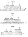
- FIGS. 2a and 2b illustrate the basic structure of a FBAR resonator with a micro-machined membrane, according to the two respective variants with a supported membrane or a cavity.
- Figure 3 illustrates the general configuration of a SMR resonator Bragg acoustic reflector.
- FIG. 4 illustrates the RF telemetry transmitter / receiver circuits and the way in which they are coupled to a common antenna, in an active dual-band device according to the invention.
- Figure 5 illustrates in more detail the structure of a BAW type SMR resonator with acoustic Bragg mirror.
- Figure 6 illustrates the structure of an asymmetric rejector filter made from a combination of scaled resonators.
- Figure 7 shows the structure of a symmetrical rejector filter made from a combination of lattice resonators.
- FIGS. 8, 9 and 10 illustrate three possible integration or transfer techniques of the SMR resonators on an RF telemetry circuit according to the invention.
- FIG. 1 schematically shows the configuration of an RF telemetry circuit of an active medical device according to the prior art.
- the main circuit 10 typically realized on a hybrid substrate, comprises an RF telemetry transmitter / receiver circuit 12 coupled to an antenna 14 incorporated in the device (for example in the region of the connection head of the implant).
- the rejection of the spurious signals is ensured by the interposition between the antenna 14 and the circuits 12 of a resonator 16 such as a SAW surface acoustic wave or BAW 16 acoustic wave resonator.
- impedance 18, 20 are provided as needed to ensure possible coupling and symmetrization as well as to reduce insertion losses.
- the component 22 comprises a layer 24 of piezoelectric material excited by conductive electrodes 26, 28. When it is stressed, this material transmits a fraction of its energy to a membrane 30 of non-piezoelectric material , micro-machined on a solid substrate 32. On the other hand, a portion 34 of this solid substrate 32 has been eliminated locally, so as to form a cavity 34 which may be excited by the vibration of the apparent portion 36 of the membrane .
- the substrate 32 is kept intact, and the cavity 34 is formed by reserving an air gap between the resonator 24 and the substrate 32.
- This interval is for example obtained in depositing a sacrificial layer between resonator and substrate so that once this layer removed the resonator 24 is suspended above the substrate.
- the starting point of the invention consists in choosing for the band rejection filter a resonator structure other than that of the FBAR resonator illustrated in FIGS. 2a and 2b.
- the invention proposes to use, in an RF telemetry circuit for an active medical device, in particular for an active implant, a resonator of the SMR ( Solidly Mounted Resonator ) type, which is a different configuration of piezoelectric resonator, related to substrate and not using any cavity or membrane.
- SMR Solidly Mounted Resonator
- FIG. 3 The general structure of a SMR type component is illustrated in FIG. 3.
- This component consists of a resonator 40 comprising a layer 24 of piezoelectric material, for example aluminum nitride AIN, placed between two metal layers 26, 28 forming excitation electrodes, for example in molybdenum.
- a resonator 40 comprising a layer 24 of piezoelectric material, for example aluminum nitride AIN, placed between two metal layers 26, 28 forming excitation electrodes, for example in molybdenum.
- the resonant structure is acoustically isolated from the substrate 32 by an interface composed of a stack 42 of quarter-wave layers of very different acoustic impedances. alternatively high and low, making it possible to produce an acoustic Bragg mirror.
- the layers constituting the stack 42 are, for example, alternating layers of silicon nitride SiN and silicon oxycarbide SiOC, and their number can be as high as ten, twelve or more.
- US-2004/0140869 we can refer to US-2004/0140869 above, which explains the theory and electrical performance of such a component.
- This resonator has the advantage of being able to be realized on a very large variety of substrates (the acoustic properties of the substrate being unimportant) and to be also integrable into the overall manufacturing process of the monolithic circuit with which the resonator will be associated.
- FIG. 4 illustrates the configuration of a dual-band RF telemetry circuit using such an SMR resonator, for example an RF telemetry circuit capable of operating indifferently in the 402-405 MHz and 2.4 GHz bands.
- the RF telemetry circuit 10 comprises two respective transmitter / receiver stages 12, 44 operating in each of the two bands concerned. These circuits have a similar structure, with a low noise amplifier LNA 46 receiving side and a PA 48 power amplifier transmitting side. These reception and transmission amplifiers 46, 48 are coupled to various mixer stages 50 and to a controlled oscillator. voltage VCO 52. The assembly is controlled by data input signals in phase E I and quadrature E Q and by a control signal of the frequency of the oscillator VCO, and outputs data signals by phase S l and in quadrature S Q.
- the two transmitting / receiving circuits 12, 44 are coupled to a common antenna 14, for example a doublet incorporated in the housing of the implant and connected by a symmetrical two-wire line to each of the two transmit / receive circuits.
- the circuit 12 operating in the band 402-405 MHz is, in a manner known per se, coupled to the antenna 14 by means of a rejector filter 16 comprising a surface acoustic wave resonator SAW, with elements appropriate 18, 20 impedance matching.
- the circuit 44 operating in the 2.4 GHz band is coupled to the antenna 14 via a rejector filter 54 comprising a BAW resonator type SMR, or a combination of several resonators of this type (see below) .
- the coupling of the filter 54 to the rest of the circuit is ensured by respective elements referenced 56 on the antenna side, 58 on the receiving side and 60 on the transmitting side.
- the search for the best band is performed, and data transmission is performed on the selected band.
- the electronic circuits of the band that has not been chosen are put in a low consumption mode, so as to reduce by the same energy consumed by the stack of the implant.
- Figure 5 further describes the SMR type BAW resonator used (alone or in combination) as a band rejection filter for the device of the invention.
- this resonator is formed during the same process as the RF telemetry transmitter / receiver circuit, that is to say that the RF chip is a monolithic chip integrating its own SMR resonator.
- the resonator 40 comprises a piezoelectric layer 24, for example aluminum nitride AIN, disposed between two metal excitation electrodes 26, 28, for example molybdenum.
- a piezoelectric layer for example aluminum nitride AIN
- metal excitation electrodes 26, 28, for example molybdenum When an RF signal is applied between these two electrodes, a mechanical deformation is created in the material and, for a predetermined frequency, the waves become stronger and the component resonates.
- the resonator is characterized by its natural frequency, its coupling coefficient (representative of insertion losses) and its quality factor.
- the natural frequency is determined by various parameters such as the acoustic velocity in the material, its Young's modulus and the thickness of the various layers of the component.
- this one must be isolated from the substrate 32 on which it is formed so that the resonance can be established with a good coupling coefficient.
- this isolation is achieved by a stack 42 of SiN / SiOC layers forming an acoustic Bragg reflector. The thickness of each layer depends on the natural frequency of the resonator (quarter wave) and the number of layers is calculated to optimize the final reflection, typically at least 99% of the acoustic signal being reflected.
- the layer 24 is dug, for example at 64, 66, 68, and coated with a metallization, until reaching the vias such as 70, 72 formed through the Bragg mirror stack 42, in end regions beyond the region of the piezoelectric layer 24 driven in vibration by electrically biasing the electrodes 26, 28.
- the resonator 40 comprises on its upper surface a charge layer 74, for example of SiO 2 , which is electrically neutral but whose effect is, because of its mass, to influence the natural frequency of the resonant structure.
- This layer allows, by selective controlled removal of material (eg laser or ion beam erosion) to gradually remove a reduced amount of material until the desired precise resonance frequency (trimming).
- a passivation layer 76 of silicon nitride SiN) protects the structure of the resonator once it is tuned to the chosen natural frequency.
- Figures 6 and 7 illustrate two examples of combinations of SMR type BAW resonators such as the one just described, to obtain a band rejection filter having the desired performance.
- FIG. 6 illustrates a band rejection filter 54 with asymmetric I / O input / output, the resonators being associated in a ladder arrangement, for example eight resonators, with four parallel resonators 78 and four 80 series resonators. parallel have resonance frequencies slightly offset, the bandwidth of the filter 54 being related to this shift, with a resonant frequency of parallel resonators corresponding to the antiresonance frequency of the series resonators to minimize insertion losses.
- FIG. 7 illustrates another possible combination of four parallel resonators 78 and four series resonators 80 in a lattice configuration, adapted to the production of a symmetrical filter, for differential circuits.
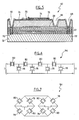
- FIGS. 8 to 10 illustrate several technological solutions for associating resonators 40, in particular combined with several to produce a band rejection filter, with the monolithic chip 44 of the RF telemetry / transmitter / receiver circuit, this chip being itself reported on a hybrid circuit board 82 supporting and interconnecting all the active and passive components of the medical device.
- the first solution illustrated in FIG. 8, consists in producing the various resonators 40 directly on the surface of the chip 44, in an integrated manner during the same process step.
- FR-A-2,853,473 describes an electronic component incorporating one or more associated resonators, made monolithically.
- the second solution illustrated in FIG. 9, consists in producing the resonators in the form of discrete autonomous components and then in transferring them to the chip 44, for example by a flip-chip technique or the like.
- the production efficiency can be increased by pre-sorting the resonators before they are transferred to chip 44.
- the third solution illustrated in FIG. 10, consists in also making the resonators 40 in the form of discrete components, and in transferring them no longer to the chip 44, but to the hybrid circuit board 82 receiving, moreover, the circuit chip 44. .
- the first two techniques are compatible with a stack of monolithic chips, where the chip of the RF telemetry / transmitter circuits is for example stacked on the chip of the signal processing microcontroller, instead of being arranged next to it.
- This configuration has the advantage of saving the space available for the electronic circuits inside the implant housing.
- the integration of the resonators above the RF telemetry chip, itself superimposed on the chip of the microcontroller, involves only an increase in overall thickness of the stack by a few tens of micrometers more, negligible on the clutter plan.
- Another advantage of this stacked configuration is that it greatly reduces impedances, in particular the distributed inductances of the connecting conductors, tracks, bonds, etc. and avoids having to re-connect the resonator of the rejection filter (or the different resonators combined to form this rejection filter) after transfer to the chip.
Abstract
Description
L'invention concerne les "dispositifs médicaux actifs" tels que définis par la directive 93/42/CE du 14 juin 1993 du Conseil des communautés européennes, et notamment les "dispositifs médicaux implantables actifs" tels que définis par la directive du Conseil 90/385/CEE du 20 juin 1990.The invention relates to "active medical devices" as defined by Directive 93/42 / EC of 14 June 1993 of the Council of the European Communities, and in particular "active implantable medical devices" as defined by Council Directive 90 / 385 / EEC of 20 June 1990.
Cette définition inclut en particulier les appareils chargés de surveiller l'activité cardiaque et de générer des impulsions de stimulation, de resynchronisation, de défibrillation et/ou de cardioversion en cas de trouble du rythme détecté par l'appareil. Elle inclut aussi les appareils neurologiques, les pompes de diffusion de substances médicales, les implants cochléaires, les capteurs biologiques implantés, etc., ainsi que les dispositifs de mesure de pH ou encore d'impédance intracorporelle (telle que mesure d'impédance transpulmonaire ou d'impédance intracardiaque). On notera également que, si l'invention s'applique de manière particulièrement avantageuse aux appareils implantés tels que stimulateurs, cardioverteurs ou défibrillateurs, elle peut tout aussi bien être mise en oeuvre avec des dispositifs médicaux non implantés, par exemple des enregistreurs de données comme les appareils Holter externes destinés à la surveillance et à l'enregistrement en ambulatoire de certains paramètres physiologiques tels que par exemple l'activité cardiaque.This definition includes in particular the devices responsible for monitoring cardiac activity and generating pacing, resynchronization, defibrillation and / or cardioversion pulses in the event of arrhythmia detected by the device. It also includes neurological devices, medical substance delivery pumps, cochlear implants, implanted biological sensors, etc., as well as devices for measuring pH or intracorporeal impedance (such as trans-pulmonary impedance measurement or intracardiac impedance). It will also be noted that, while the invention applies particularly advantageously to implanted devices such as pacemakers, cardiovers or defibrillators, it can equally well be implemented with non-implanted medical devices, for example data loggers such as external Holter devices for ambulatory monitoring and recording of certain physiological parameters such as, for example, cardiac activity.
De façon générale, la plupart des dispositifs médicaux actifs sont conçus pour permettre un échange de données avec un "programmateur", qui est un appareil externe permettant de vérifier le paramétrage du dispositif, de lire des informations enregistrées par celui-ci ou d'y inscrire des informations, ou encore de mettre à jour le logiciel interne de pilotage du dispositif.In general, most active medical devices are designed to allow a data exchange with a "programmer", which is an external device for verifying the setting of the device, read information recorded by it or therein register information, or update the internal software control device.
Cet échange de données entre le dispositif médical et le programmateur est effectué par télémétrie, c'est-à-dire par une technique de transmission à distance d'informations, sans contact galvanique.This exchange of data between the medical device and the programmer is performed by telemetry, that is to say by a technique of remote transmission of information, without galvanic contact.
Jusqu'à présent, la télémétrie est opérée par couplage essentiellement inductif entre des bobines du dispositif implanté et du programmateur, technique connue sous le nom de "procédé par induction". Cette technique présente cependant l'inconvénient, en raison de la très faible portée d'un couplage inductif, de nécessiter l'utilisation d'une "tête de télémétrie" reliée au programmateur et contenant une bobine qu'un opérateur place au voisinage du site où est implanté le dispositif.Until now, the telemetry is operated by essentially inductive coupling between the coils of the implanted device and the programmer, a technique known as the "induction method". However, this technique has the disadvantage, because of the very low range of inductive coupling, to require the use of a "telemetry head" connected to the programmer and containing a coil that an operator places in the vicinity of the site where the device is implanted.
Il a été récemment proposé de mettre en oeuvre une autre technique de couplage non galvanique, utilisant les deux composantes d'une onde électromagnétique produite par des circuits émetteurs/récepteurs opérant dans le domaine des radiofréquences (RF), typiquement des fréquences de l'ordre de plusieurs centaines de mégahertz.It has recently been proposed to implement another non-galvanic coupling technique, using the two components of an electromagnetic wave produced by transmitter / receiver circuits operating in the field of radio frequencies (RF), typically frequencies of the order several hundred megahertz.
Cette technique, dite de "télémétrie RF" permet de programmer ou interroger des implants à des distances supérieures à 3 m, et autorise donc l'échange d'informations sans manipulation d'une tête de télémétrie, voire même sans intervention d'un opérateur externe.This technique, called "RF telemetry" allows programming or interrogating implants at distances greater than 3 m, and therefore allows the exchange of information without manipulation of a telemetry head, or even without the intervention of an operator external.
Un dispositif comprenant des moyens de télémétrie RF, et son programmateur associé, sont par exemple décrits dans le
Le fonctionnement satisfaisant des circuits de télémétrie RF implique une élimination efficace des parasites RF susceptibles de produire des interférences et de perturber la transmission des données. En effet, à la différence des techniques par induction, qui présentent une bonne immunité aux parasites, la réception des signaux RF est fortement perturbée par l'environnement électromagnétique, notamment les signaux de radio, de télévision et de téléphonie mobile, sans compter les nombreux parasites industriels susceptibles d'être produits dans l'environnement immédiat du porteur de l'implant.The satisfactory operation of RF telemetry circuits involves the efficient removal of RF interference that can cause interference and disrupt data transmission. Indeed, unlike inductive techniques, which have good immunity to interference, the reception of RF signals is strongly disturbed by the electromagnetic environment, including radio, television and mobile telephony signals, not to mention the numerous industrial pests likely to be produced in the immediate environment of the implant wearer.
Les circuits de télémétrie RF nécessitent donc l'utilisation de filtres passe-bande très efficaces, présentant une caractéristique de réjection de bande très abrupte.RF telemetry circuits therefore require the use of very efficient bandpass filters, having a very abrupt band rejection characteristic.
Les filtres à ondes acoustiques présentent de telles propriétés, et le
Ces filtres à résonateur SAW ou FBAR présentent cependant un certain nombre d'inconvénients, tout particulièrement lorsqu'ils sont utilisés dans des dispositifs implantés.These SAW or FBAR resonator filters, however, have a number of disadvantages, especially when used in implanted devices.
Ainsi, les résonateurs SAW utilisent, par principe, la propagation d'une onde acoustique en surface, qui implique corrélativement une taille de composant relativement importante. Cet inconvénient est particulièrement handicapant avec les dispositifs implantés qui, comme on le comprend aisément, requièrent une miniaturisation poussée du circuit électronique compte tenu de la place réduite disponible à l'intérieur du boîtier.Thus, the SAW resonators use, in principle, the propagation of a surface acoustic wave, which correlatively implies a relatively large component size. This disadvantage is particularly disabling with the implanted devices which, as is easily understood, require extensive miniaturization of the electronic circuit given the reduced space available inside the housing.
D'autre part, du point de vue de la technologie, ces résonateurs SAW sont disponibles seulement sous forme de composants discrets, qui doivent donc être reportés sur le circuit électronique de l'implant, avec les inconvénients qui en découlent en termes notamment d'étapes de procédé supplémentaires et de coût supérieur.On the other hand, from the point of view of technology, these SAW resonators are available only in the form of discrete components, which must therefore be reported on the electronic circuit of the implant, with the resulting drawbacks in terms in particular of additional process steps and higher cost.
Enfin, sur le plan électrique, les résonateurs SAW présentent une excellente sélectivité mais introduisent des pertes d'insertion non négligeables dans les circuits où ils sont utilisés, dégradant d'autant la sensibilité du récepteur de télémétrie.Finally, in electrical terms, the SAW resonators have excellent selectivity but introduce significant insertion losses in the circuits where they are used, thereby degrading the sensitivity of the telemetry receiver.
A la différence des résonateurs SAW, les résonateurs FBAR présentent une taille beaucoup plus réduite et des pertes d'insertion moindres.Unlike SAW resonators, FBAR resonators have a much smaller size and lower insertion losses.
En revanche, ces résonateurs FBAR sont beaucoup plus délicats à réaliser, car ils nécessitent le micro-usinage d'une très fine membrane mobile, susceptible d'être mise en résonance (on décrira plus en détail la structure des résonateurs FBAR en référence aux figures 2a et 2b). Ce micro-usinage est délicat à mettre en oeuvre, notamment dans un processus collectif, ce qui introduit de nombreux rebuts lors de la fabrication des composants.On the other hand, these FBAR resonators are much more delicate to produce, because they require the micromachining of a very thin mobile membrane, capable of being resonated (the structure of the FBAR resonators will be described in more detail with reference to FIGS. 2a and 2b). This micro-machining is difficult to implement, especially in a collective process, which introduces many rejects during the manufacture of components.
De plus, le mouvement de la membrane mobile implique de laisser subsister un espace libre au-dessus et au-dessous de celle-ci. De ce fait, si des poussières venaient à se déposer au-dessus de la membrane en cours de fabrication ou postérieurement, la fréquence de résonance de la membrane se trouverait modifiée, et il serait nécessaire de réaccorder le filtre. Pour pallier cet inconvénient, une fois réalisé et ajusté en fréquence, le composant doit être enfermé dans un volume étanche, avec formation d'une couche supplémentaire ou report d'un capot de fermeture du composant.In addition, the movement of the mobile membrane involves leaving a free space above and below it. Therefore, if dusts were deposited above the membrane during manufacture or later, the resonant frequency of the membrane would be modified, and it would be necessary to re-connect the filter. To overcome this drawback, once realized and adjusted in frequency, the component must be enclosed in a sealed volume, with formation an additional layer or carry a closing cap of the component.
Du point de vue industriel, bien qu'il soit théoriquement possible d'intégrer le résonateur FBAR au cours du processus de fabrication du circuit auquel il est associé, une telle intégration se révèle difficile à mettre en oeuvre avec un rendement satisfaisant, de sorte que les résonateurs FBAR aujourd'hui disponibles le sont seulement sous forme de composants discrets. Le composant FBAR doit donc être reporté sur le circuit électronique ou sur la plaquette hybride par un procédé additionnel tel que wire-bonding ou flip-chip, ce qui, comme dans le cas du SAW, grève le coût de fabrication et réduit les performances électriques du fait de la présence des fils, pistes de liaison, etc.From the industrial point of view, although it is theoretically possible to integrate the FBAR resonator during the manufacturing process of the circuit with which it is associated, such integration proves difficult to implement with satisfactory performance, so that FBAR resonators available today are only in the form of discrete components. The FBAR component must therefore be transferred to the electronic circuit or the hybrid wafer by an additional method such as wire-bonding or flip-chip, which, as in the case of SAW, strike the manufacturing cost and reduces the electrical performance. because of the presence of wires, tracks, etc.
Enfin, outre la difficulté qu'il y a à trouver et maintenir l'accord d'un composant résonateur FBAR, celui-ci présente une caractéristique de réjection moins abrupte que celle d'un résonateur SAW, de sorte que pour obtenir une réjection satisfaisante, il est nécessaire de combiner entre eux plusieurs résonateurs FBAR. Cette multiplication des composants augmente d'autant le coût, l'encombrement, et les difficultés de mise au point du circuit final.Finally, in addition to the difficulty of finding and maintaining the tuning of a FBAR resonator component, it has a rejection characteristic less abrupt than that of a SAW resonator, so that to obtain a satisfactory rejection it is necessary to combine several FBAR resonators. This multiplication of components increases all the cost, congestion, and difficulties of development of the final circuit.
Le problème de l'invention est de réaliser un dispositif médical actif, et/ou son programmateur associé, comprenant des circuits de télémétrie RF dépourvus de résonateurs FBAR pour remédier aux inconvénients ci-dessus, et qui soient adaptés aux contraintes particulières des implants actifs qui requièrent une miniaturisation plus poussée du circuit électronique compte tenu de la place réduite disponible à l'intérieur du boîtier de l'implant.The problem of the invention is to provide an active medical device, and / or its associated programmer, comprising RF telemetry circuits devoid of FBAR resonators to overcome the above drawbacks, and which are adapted to the particular constraints of active implants which require further miniaturization of the electronic circuit given the reduced space available inside the implant housing.
L'invention a notamment pour but de réaliser un tel dispositif et/ou programmateur dont les circuits RF présentent les avantages suivants :
- coût de fabrication réduit ;
- filtre éventuellement intégrable, de manière à pouvoir obtenir un composant monolithique incluant la puce du circuit émetteur/récepteur RF avec son filtre réjecteur de bande associé. Une telle intégration présente de nombreux avantages : réduction du coût d'ensemble, diminution des pertes d'insertion et maximisation de la surface utile (pour miniaturiser les implants, on sait aujourd'hui empiler plusieurs puces monolithiques les unes sur les autres ;
- réalisation collective possible avec un bon rendement du processus de fabrication (moindres rebuts) ;
- réduction des impédances parasites, notamment des inductances (conducteurs de liaison, pistes, bondings, etc.), permettant de réduire les pertes d'insertion et éviter d'avoir à réaccorder le filtre après intégration ou report sur le circuit ;
- possibilité d'utilisation en nombre des résonateurs, permettant de concevoir des filtres performants combinant plusieurs résonateurs pour obtenir une caractéristique très abrupte.
- reduced manufacturing cost;
- optionally integrable filter, so as to obtain a monolithic component including the RF transmitter / receiver circuit chip with its associated band rejection filter. Such integration has many advantages: reducing the overall cost, reducing insertion losses and maximizing the usable area (for miniaturize implants, we know today stack several monolithic chips on top of each other;
- collective realization possible with a good efficiency of the manufacturing process (less scrap);
- reduction of parasitic impedances, in particular of inductances (connecting conductors, tracks, bonds, etc.), making it possible to reduce insertion losses and to avoid having to re-connect the filter after integration or transfer to the circuit;
- possibility of use in number of the resonators, allowing to design powerful filters combining several resonators to obtain a very abrupt characteristic.
Un autre but de l'invention est de proposer un dispositif actif comportant des circuits de télémétrie RF susceptibles de fonctionner dans plusieurs bandes de fréquences, telles que la bande MICS (Medical Implants Communication System) 402-405 MHz, ou les bandes banalisées publiques ISM (Industriel, Scientifique et Médical) 863-870 MHz, 902-928 MHz et 2,4 GHz utilisées par les dispositifs médicaux, ou encore une transmission de type Ultra Wide Band UWB, qui est une technique où les signaux émis sont des impulsions de Dirac produisant dans le domaine fréquentiel un très large spectre (donc sans filtrage dans ce dernier cas).Another object of the invention is to propose an active device comprising RF telemetry circuits capable of operating in several frequency bands, such as the 402-405 MHz Medical Implants Communication System ( MICS ) band, or the ISM public unmarked bands. (Industrial, Scientific and Medical) 863-870 MHz, 902-928 MHz and 2.4 GHz used by medical devices, or a UWB Ultra Wide Band transmission, which is a technique where the signals emitted are pulses of Dirac producing in the frequency domain a very broad spectrum (thus without filtering in the latter case).
En effet, les appareils dotés de fonctions de télémétrie RF actuels sont tous des appareils seulement multicanaux, c'est-à-dire utilisant plusieurs fréquences situées dans une même bande.Indeed, devices equipped with current RF telemetry functions are all devices only multichannel, that is to say, using several frequencies in the same band.
Or il serait particulièrement avantageux de disposer d'un appareil multi-bande (bibande, tribande, voire même quadribande), car :
- les bandes de fréquences autorisées ne sont pas forcément les mêmes selon les pays ;
- selon les circonstances, la propagation peut être meilleure dans telle ou telle bande, et il serait avantageux de pouvoir choisir celle qui assure la meilleure propagation de manière à optimiser la transmission des données ;
- l'occupation de la bande (le nombre de canaux utilisés) varie selon les bandes et, là encore, il pourrait être avantageux de choisir une bande présentant suffisamment de canaux libres.
- the authorized frequency bands are not necessarily the same according to the country;
- depending on the circumstances, the propagation may be better in this or that band, and it would be advantageous to be able to choose the one that ensures the best propagation so as to optimize the transmission of the data;
- the occupation of the band (the number of channels used) varies according to the bands and, again, it could be advantageous to choose a band having sufficient free channels.
Le problème de l'invention est résolu, et les différents buts précités sont atteints, par un dispositif médical actif, ou son programmateur associé, du type général comprenant, comme divulgué par le
Une telle structure de résonateur est décrite dans le
Très avantageusement, le dispositif de l'invention comprend une pluralité d'émetteurs/récepteurs de télémétrie RF opérant dans des bandes de fréquences respectives distinctes, notamment au moins deux des bandes 402-405 MHz, 863-870 MHz, 902-928 MHz ou 2,4 GHz, ou encore une transmission large bande de type UWB. Chaque émetteur/récepteur (sauf en UWB) comporte un filtre de réjection de bande respectif, dont l'un au moins inclut au moins un résonateur BAW à ondes acoustiques de volume du type SMR à isolement par miroir de Bragg acoustique.Very advantageously, the device of the invention comprises a plurality of RF telemetry transmitters / receivers operating in respective respective frequency bands, in particular at least two of the bands 402-405 MHz, 863-870 MHz, 902-928 MHz or 2.4 GHz, or a broadband transmission UWB type. Each transmitter / receiver (except UWB) includes a respective band rejection filter, at least one of which includes at least one acoustic wave BAW resonator of the SMR type with acoustic Bragg mirror isolation.
L'antenne du dispositif peut être commune aux différents émetteurs/récepteurs, et couplée à ces derniers par l'intermédiaire des filtres de réjection de bande et d'éléments d'adaptation d'impédance.The antenna of the device may be common to the different transmitters / receivers, and coupled thereto through the band rejection filters and impedance matching elements.
Il est avantageusement prévu des moyens d'évaluation de la performance des différentes bandes de fréquences, et des moyens de sélection de celui des émetteurs/récepteurs opérant dans celle de ces bandes et présentant la meilleure performance en termes de transmission des signaux de télémétrie RF. Ces moyens d'évaluation peuvent notamment évaluer des critères parmi le niveau de signal capté en réception, le débit maximal de données susceptible d'être transmis, et l'occupation des différents canaux dans les bandes respectives. Il peut être également prévu des moyens pour commuter en un mode de faible consommation le ou les émetteurs/récepteurs opérant dans la ou les bandes non sélectionnées.It is advantageously provided with means for evaluating the performance of the different frequency bands, and means for selecting the one of the transmitters / receivers operating in the one of these bands and having the best performance in terms of transmission of the RF telemetry signals. These evaluation means can notably evaluate criteria among the signal level received in reception, the maximum data rate that can be transmitted, and the occupation of the different channels in the respective bands. Means may also be provided for switching in a low power mode the transmitter (s) / receiver (s) operating in the non-selected band (s).
Le dispositif de l'invention est typiquement réalisé avec une plaquette de circuit hybride et au moins une puce de circuit monolithique, reportée sur cette plaquette, intégrant le(s)dit(s) émetteur(s)/récepteur(s) de télémétrie RF. Le résonateur BAW peut alors être soit directement intégré à la puce en surface de celle-ci, soit réalisé sous forme d'un composant discret, distinct de la puce, reporté en surface de celle-ci ou bien en surface de la plaquette de circuit hybride.The device of the invention is typically realized with a hybrid circuit board and at least one monolithic circuit chip, carried on this board, integrating the said transmitter (s) / RF telemetry receiver (s). . The BAW resonator can then either be integrated directly into the chip on the surface thereof, or be in the form of a discrete component, distinct from the chip, carried on the surface thereof or on the surface of the circuit board. hybrid.
Très avantageusement, le résonateur BAW est un résonateur accordable comprenant une couche superficielle de charge érodable.Very advantageously, the BAW resonator is a tunable resonator comprising a surface layer of erodable charge.
Le filtre de réjection de bande peut être un filtre à entrée et sortie différentielles comprenant une pluralité de résonateurs BAW configurés en treillis, ou bien un filtre à entrée et sortie asymétriques comprenant une pluralité de résonateurs BAW configurés en échelle.The band rejection filter may be a differential input and output filter comprising a plurality of lattice-configured BAW resonators, or an asymmetric input and output filter comprising a plurality of ladder-configured BAW resonators.
On va maintenant décrire un exemple de réalisation de l'invention, en référence aux dessins annexés où les mêmes références numériques désignent d'une figure à l'autre des éléments identiques ou fonctionnellement semblables.An embodiment of the invention will now be described with reference to the accompanying drawings, in which the same reference numerals designate identical or functionally similar elements from one figure to another.
La figure 1 illustre, de façon schématique, un circuit émetteur/récepteur de télémétrie RF couplé à son antenne associée, dans le cas d'un dispositif de l'art antérieur.FIG. 1 schematically illustrates an RF telemetry transmitter / receiver circuit coupled to its associated antenna, in the case of a device of the prior art.
Les figures 2a et 2b illustrent la structure de principe d'un résonateur de type FBAR à membrane micro-usinée, selon les deux variantes respectives à membrane supportée ou à cavité.FIGS. 2a and 2b illustrate the basic structure of a FBAR resonator with a micro-machined membrane, according to the two respective variants with a supported membrane or a cavity.
La figure 3 illustre la configuration générale d'un résonateur de type SMR à réflecteur acoustique de Bragg.Figure 3 illustrates the general configuration of a SMR resonator Bragg acoustic reflector.
La figure 4 illustre les circuits émetteurs/récepteurs de télémétrie RF et la manière dont ils sont couplés à une antenne commune, dans un dispositif actif de type bi-bande selon l'invention.FIG. 4 illustrates the RF telemetry transmitter / receiver circuits and the way in which they are coupled to a common antenna, in an active dual-band device according to the invention.
La figure 5 illustre de façon plus détaillée la structure d'un résonateur BAW de type SMR à miroir de Bragg acoustique.Figure 5 illustrates in more detail the structure of a BAW type SMR resonator with acoustic Bragg mirror.
La figure 6 illustre la structure d'un filtre réjecteur asymétrique réalisé à partir d'une combinaison de résonateurs montés en échelle.Figure 6 illustrates the structure of an asymmetric rejector filter made from a combination of scaled resonators.
La figure 7 montre la structure d'un filtre réjecteur symétrique, réalisé à partir d'une combinaison de résonateurs montés en treillis.Figure 7 shows the structure of a symmetrical rejector filter made from a combination of lattice resonators.
Les figures 8, 9 et 10 illustrent trois techniques possibles d'intégration ou de report des résonateurs SMR sur un circuit de télémétrie RF selon l'invention.FIGS. 8, 9 and 10 illustrate three possible integration or transfer techniques of the SMR resonators on an RF telemetry circuit according to the invention.
Sur la figure 1, on a représenté de façon schématique la configuration d'un circuit de télémétrie RF d'un dispositif médical actif selon la technique antérieure.FIG. 1 schematically shows the configuration of an RF telemetry circuit of an active medical device according to the prior art.
Le circuit principal 10, typiquement réalisé sur un substrat hybride, comprend un circuit émetteur/récepteur de télémétrie RF 12 couplé à une antenne 14 incorporée au dispositif (par exemple dans la région de la tête de connexion de l'implant).The
La réjection des signaux parasites est assurée par interposition entre l'antenne 14 et les circuits 12 d'un résonateur 16 tel qu'un résonateur à onde acoustique de surface SAW ou à onde acoustique de volume BAW 16. Des composants d'adaptation d'impédance 18, 20 sont prévus en tant que de besoin pour assurer le couplage et la symétrisation éventuelle ainsi que pour réduire les pertes d'insertion.The rejection of the spurious signals is ensured by the interposition between the
Lorsque les filtres de réjection des circuits de télémétrie RF des implants connus mettent en oeuvre des résonateurs BAW, ceux-ci sont des composants de type FBAR présentant l'une des deux structures illustrées figure 2a et 2b.When the RF telemetry circuit rejection filters of the known implants use BAW resonators, these are FBAR type components having one of the two structures illustrated in FIGS. 2a and 2b.
Dans la première structure, illustrée figure 2a, le composant 22 comprend une couche 24 de matériau piézoélectrique excité par des électrodes conductrices 26, 28. Lorsqu'il est sollicité, ce matériau transmet une fraction de son énergie à une membrane 30 en matériau non piézoélectrique, micro-usinée sur un substrat massif 32. D'autre part, une partie 34 de ce substrat massif 32 a été éliminée localement, de manière à former une cavité 34 qui pourra être excitée par la vibration de la partie apparente 36 de la membrane.In the first structure, illustrated in FIG. 2a, the
Dans la seconde variante, illustrée figure 2a, le substrat 32 est conservé intact, et la cavité 34 est formée en réservant un intervalle d'air entre le résonateur 24 et le substrat 32. Cet intervalle est par exemple obtenu en déposant une couche sacrificielle entre résonateur et substrat de sorte qu'une fois cette couche enlevée le résonateur 24 se trouve suspendu au-dessus du substrat.In the second variant, illustrated in FIG. 2a, the
Comme on le comprend aisément, ces structures sont délicates à réaliser et fragiles. De plus, l'ajustement de la fréquence de résonance du composant dépend très fortement des propriétés du matériau piézoélectrique, de l'épaisseur des couches, du dimensionnement de la cavité résonante et des diverses contraintes mécaniques exercées sur la membrane, qui a tendance à se déformer et à se déchirer aisément.As is easily understood, these structures are delicate to achieve and fragile. In addition, the adjustment of the resonant frequency of the component depends very strongly on the properties of the piezoelectric material, the thickness of the layers, the resonant cavity design and the various mechanical stresses exerted on the membrane, which tends to deform and tear easily.
Le point de départ de l'invention consiste à choisir pour le filtre de réjection de bande une structure de résonateur autre que celle du résonateur FBAR illustrée sur les figures 2a et 2b.The starting point of the invention consists in choosing for the band rejection filter a resonator structure other than that of the FBAR resonator illustrated in FIGS. 2a and 2b.
Plus précisément, l'invention propose d'utiliser, dans un circuit de télémétrie RF pour dispositif médical actif, notamment pour un implant actif, un résonateur de type SMR (Solidly Mounted Resonator), qui est une configuration différente de résonateur piézoélectrique, liée au substrat et ne mettant en oeuvre aucune cavité ni membrane.More specifically, the invention proposes to use, in an RF telemetry circuit for an active medical device, in particular for an active implant, a resonator of the SMR ( Solidly Mounted Resonator ) type, which is a different configuration of piezoelectric resonator, related to substrate and not using any cavity or membrane.
La structure générale d'un composant de type SMR est illustrée figure 3. Ce composant est constitué d'un résonateur 40 comprenant une couche 24 de matériau piézoélectrique, par exemple du nitrure d'aluminium AIN, disposée entre deux couches métalliques 26, 28 formant électrodes d'excitation, par exemple en molybdène.The general structure of a SMR type component is illustrated in FIG. 3. This component consists of a
Pour éviter que l'onde acoustique ne s'y propage et ne s'y atténue, la structure résonante est acoustiquement isolée du substrat 32 par une interface composée d'un empilement 42 de couches quart d'onde d'impédances acoustiques très différentes, alternativement élevées et faibles, permettant de réaliser un miroir de Bragg acoustique. Les couches constituant l'empilement 42 sont par exemple des couches alternées de nitrure de silicium SiN et oxycarbure de silicium SiOC, et leur nombre peut atteindre dix ou douze, voire plus. Pour plus de détails, on pourra se référer au
Ce résonateur présente l'avantage de pouvoir être réalisé sur une très grande variété de substrats (les propriétés acoustiques du substrat étant sans importance) et d'être également intégrable au processus global de fabrication du circuit monolithique auquel sera associé le résonateur.This resonator has the advantage of being able to be realized on a very large variety of substrates (the acoustic properties of the substrate being unimportant) and to be also integrable into the overall manufacturing process of the monolithic circuit with which the resonator will be associated.
La figure 4 illustre la configuration d'un circuit de télémétrie RF bibande utilisant un tel résonateur SMR, par exemple un circuit de télémétrie RF susceptible de fonctionner indifféremment dans les bandes 402-405 MHz et 2,4 GHz.FIG. 4 illustrates the configuration of a dual-band RF telemetry circuit using such an SMR resonator, for example an RF telemetry circuit capable of operating indifferently in the 402-405 MHz and 2.4 GHz bands.
Le circuit de télémétrie RF 10 comprend deux étages émetteur/récepteur respectifs 12, 44 fonctionnant dans chacune des deux bandes concernées. Ces circuits présentent une structure semblable, avec côté réception un amplificateur faible bruit LNA 46 et côté émission un amplificateur de puissance PA 48. Ces amplificateurs de réception et d'émission 46, 48 sont couplés à divers étages mélangeurs 50 et à un oscillateur commandé en tension VCO 52. L'ensemble est contrôlé par des signaux d'entrée de données en phase EI et en quadrature EQ et par un signal de commande de la fréquence de l'oscillateur VCO, et délivre en sortie des signaux de données en phase Sl et en quadrature SQ. Les deux circuits d'émission/réception 12, 44 sont couplés à une antenne commune 14, par exemple un doublet incorporé au boîtier de l'implant et relié par une ligne symétrique bifilaire à chacun des deux circuits d'émission/réception.The
Le circuit 12 opérant dans la bande 402-405 MHz est, de manière en elle-même connue, couplé à l'antenne 14 par l'intermédiaire d'un filtre réjecteur 16 comprenant un résonateur à ondes acoustiques de surface SAW, avec des éléments appropriés 18, 20 d'adaptation d'impédance. Le circuit 44 opérant dans la bande 2,4 GHz est couplé à l'antenne 14 par l'intermédiaire d'un filtre réjecteur 54 comprenant un résonateur BAW de type SMR, ou une combinaison de plusieurs résonateurs de ce type (voir plus bas). Le couplage du filtre 54 au reste du circuit est assuré par des éléments respectifs référencés 56 côté antenne, 58 côté réception et 60 côté émission.The
La liaison de télémétrie RF peut être établie indifféremment dans la bande 402-405 MHz ou dans la bande 2,4 GHz. Le choix de l'une ou l'autre bande pour la transmission des données peut être avantageusement effectué de façon automatique en fonction d'un ou plusieurs critères dont, notamment :
- le niveau de signal capté en réception RSSI (Received Signal Strength Indicator) des signaux RF reçus, dans l'une et l'autre bande, par l'implant (dans le sens de transmission programmateur → implant) et par le programmateur (dans le sens de transmission implant → programmateur)
- le débit maximal des données susceptibles d'être transmis dans l'une et l'autre bande, et/ou
- l'occupation des différents canaux dans l'une et l'autre bande, de manière à s'assurer de pouvoir disposer d'un canal de communication libre.
- level signal received in reception RSSI (Received Signal Strength Indicator) of the received RF signals in one and the other strip, for the implant (in the direction of transmission scheduler → implant) and the controller (in the direction of transmission implant → programmer)
- the maximum data rate that can be transmitted in either band, and / or
- the occupation of the different channels in the one and the other band, so as to ensure that a free communication channel is available.
Chaque fois qu'une communication de télémétrie RF est initiée, la recherche de la meilleure bande est opérée, et la transmission des données est effectuée sur la bande choisie. Avantageusement, les circuits électroniques de la bande qui n'a pas été choisie sont mis dans un mode de faible consommation, de manière à réduire d'autant l'énergie consommée par la pile de l'implant.Whenever RF telemetry communication is initiated, the search for the best band is performed, and data transmission is performed on the selected band. Advantageously, the electronic circuits of the band that has not been chosen are put in a low consumption mode, so as to reduce by the same energy consumed by the stack of the implant.
La figure 5 décrit plus en détail le résonateur BAW de type SMR utilisé (seul ou en combinaison) comme filtre de réjection de bande pour le dispositif de l'invention.Figure 5 further describes the SMR type BAW resonator used (alone or in combination) as a band rejection filter for the device of the invention.
Très avantageusement, ce résonateur est formé au cours du même processus que le circuit émetteur/récepteur de télémétrie RF, c'est-à-dire que la puce RF est une puce monolithique intégrant son propre résonateur SMR.Very advantageously, this resonator is formed during the same process as the RF telemetry transmitter / receiver circuit, that is to say that the RF chip is a monolithic chip integrating its own SMR resonator.
Comme on l'avait expliqué plus haut en référence à la figure 3, le résonateur 40 comprend une couche piézoélectrique 24, par exemple en nitrure d'aluminium AIN, disposée entre deux électrodes métalliques d'excitation 26, 28, par exemple en molybdène. Lorsqu'un signal RF est appliqué entre ces deux électrodes, une déformation mécanique est créée dans le matériau et, pour une fréquence prédéterminée, les ondes viennent se renforcer et le composant entre en résonance. Le résonateur est caractérisé par sa fréquence propre, son coefficient de couplage (représentatif des pertes d'insertion) et son facteur de qualité. La fréquence propre est déterminée par divers paramètres tels que la vitesse acoustique dans le matériau, son module d'Young et l'épaisseur des diverses couches du composant. Du fait du comportement mécanique du résonateur, celui-ci doit être isolé du substrat 32 sur lequel il est formé de manière que la résonance puisse s'établir avec un bon coefficient de couplage. Dans le cas d'un résonateur de type SMR, cet isolement est réalisé par un empilement 42 de couches SiN/SiOC formant réflecteur de Bragg acoustique. L'épaisseur de chaque couche dépend de la fréquence propre du résonateur (quart d'onde) et le nombre de couches est calculé pour optimiser la réflexion finale, typiquement au moins 99% du signal acoustique étant réfléchi. Pour assurer la liaison électrique entre les électrodes d'excitation du cristal piézoélectrique et les différents circuits de la puce, la couche 24 est creusée, par exemple en 64, 66, 68, et revêtue d'une métallisation, jusqu'à atteindre des vias tels que 70, 72 formés au travers de l'empilement 42 formant miroir de Bragg, dans des régions d'extrémité situées au-delà de la région de la couche piézoélectrique 24 entraînée en vibration par la sollicitation électrique des électrodes 26, 28.As explained above with reference to Figure 3, the
Très avantageusement, le résonateur 40 comprend à sa surface supérieure une couche de charge 74, par exemple en SiO2, qui est neutre sur le plan électrique mais qui a pour effet, du fait de sa masse, d'influer sur la fréquence propre de la structure résonante. Cette couche permet, par un enlèvement sélectif contrôlé de matière (par exemple érosion par laser ou par faisceau d'ions) d'enlever progressivement une quantité réduite de matière jusqu'à obtenir la fréquence précise de résonance souhaitée (trimming). Une couche de passivation 76 de nitrure de silicium SiN) protège la structure du résonateur une fois celui-ci accordé sur la fréquence propre choisie.Very advantageously, the
Les figures 6 et 7 illustrent deux exemples de combinaisons de résonateurs BAW de type SMR tel que celui que l'on vient de décrire, permettant d'obtenir un filtre de réjection de bande présentant les performances souhaitées.Figures 6 and 7 illustrate two examples of combinations of SMR type BAW resonators such as the one just described, to obtain a band rejection filter having the desired performance.
La figure 6 illustre un filtre de réjection de bande 54 avec entrée/sortie I/O asymétrique, les résonateurs étant associés suivant un montage en échelle, par exemple huit résonateurs, avec quatre résonateurs parallèle 78 et quatre résonateurs série 80. Les résonateurs série et parallèle ont des fréquences de résonance légèrement décalées, la bande passante du filtre 54 étant liée à ce décalage, avec une fréquence de résonance des résonateurs parallèle correspondant à la fréquence d'antirésonance des résonateurs série pour minimiser les pertes d'insertion.FIG. 6 illustrates a
La figure 7 illustre une autre combinaison possible de quatre résonateurs parallèle 78 et quatre résonateurs série 80 dans une configuration en treillis, adaptée à la réalisation d'un filtre symétrique, pour des circuits différentiels.FIG. 7 illustrates another possible combination of four
Le choix d'un SMR comme résonateur permet, compte tenu du rendement technologique élevé (peu de rebuts), de réaliser de façon monolithique un filtre de réjection de bande comprenant une pluralité de résonateurs associés, typiquement un filtre à quatre ou huit résonateurs. Compte tenu de la multiplication des résonateurs dans un même filtre, un taux de rebut trop élevé par résonateur (comme cela est le cas des FBAR) conduirait en effet à un déchet considérable pour un filtre comportant quatre ou huit de ces résonateurs, excluant une intégration poussée.The choice of an SMR as resonator makes it possible, given the high technological efficiency (few rejects), to monolithically produce a band rejection filter comprising a plurality of associated resonators, typically a filter with four or eight resonators. Given the multiplication of resonators in the same filter, a too high scrap rate per resonator (as is the case of FBAR) would indeed lead to a considerable waste for a filter comprising four or eight of these resonators, excluding integration thrust.
Les figures 8 à 10 illustrent plusieurs solutions technologiques pour associer des résonateurs 40, notamment combinés à plusieurs pour réaliser un filtre de réjection de bande, à la puce monolithique 44 du circuit émetteur/récepteur de télémétrie RF, cette puce étant elle-même reportée sur une plaquette de circuit hybride 82 supportant et interconnectant l'ensemble des composants, actifs et passifs, du dispositif médical.FIGS. 8 to 10 illustrate several technological solutions for associating
La première solution, illustrée figure 8, consiste à réaliser les divers résonateurs 40 directement en surface de la puce 44, de manière intégrée au cours de la même étape de processus. Pour plus de détails sur cette technique d'intégration, on pourra se référer au
La deuxième solution, illustrée figure 9, consiste à réaliser les résonateurs sous forme de composants discrets autonomes, puis à les reporter sur la puce 44, par exemple par une technique de type flip-chip ou analogue. Avec cette solution, le rendement de fabrication peut être augmenté par un tri préalable des résonateurs avant leur report sur la puce 44.The second solution, illustrated in FIG. 9, consists in producing the resonators in the form of discrete autonomous components and then in transferring them to the
La troisième solution, illustrée figure 10, consiste à réaliser également les résonateurs 40 sous forme de composants discrets, et à les reporter non plus sur la puce 44, mais sur la plaquette de circuit hybride 82 recevant, par ailleurs, la puce de circuit 44.The third solution, illustrated in FIG. 10, consists in also making the
On notera que les deux premières techniques sont compatibles avec un empilement des puces monolithiques, où la puce des circuits émetteurs/récepteurs de télémétrie RF est par exemple empilée sur la puce du microcontrôleur de traitement des signaux, au lieu d'être disposée à côté de celle-ci. Cette configuration présente l'avantage d'économiser la place disponible pour les circuits électroniques à l'intérieur du boîtier de l'implant. L'intégration des résonateurs au-dessus de la puce de télémétrie RF, elle-même superposée à la puce du microcontrôleur, n'implique qu'une augmentation d'épaisseur globale de l'empilement de quelques dizaines de micromètres supplémentaires, négligeable sur le plan de l'encombrement.It will be noted that the first two techniques are compatible with a stack of monolithic chips, where the chip of the RF telemetry / transmitter circuits is for example stacked on the chip of the signal processing microcontroller, instead of being arranged next to it. This configuration has the advantage of saving the space available for the electronic circuits inside the implant housing. The integration of the resonators above the RF telemetry chip, itself superimposed on the chip of the microcontroller, involves only an increase in overall thickness of the stack by a few tens of micrometers more, negligible on the clutter plan.
Un autre avantage de cette configuration empilée est qu'elle permet de réduire fortement les impédances, notamment les inductances réparties des conducteurs de liaison, pistes, bondings, etc. et évite d'avoir à réaccorder le résonateur du filtre de réjection (ou les différents résonateurs combinés pour former ce filtre de réjection) après report sur la puce.Another advantage of this stacked configuration is that it greatly reduces impedances, in particular the distributed inductances of the connecting conductors, tracks, bonds, etc. and avoids having to re-connect the resonator of the rejection filter (or the different resonators combined to form this rejection filter) after transfer to the chip.
Claims (13)
Applications Claiming Priority (1)
| Application Number | Priority Date | Filing Date | Title |
|---|---|---|---|
| FR0604933A FR2901708A1 (en) | 2006-06-02 | 2006-06-02 | ACTIVE MEDICAL DEVICE SUCH AS ACTIVE AMPLANT OR PROGRAMMER FOR SUCH AN IMPLANT, COMPRISING RF EMITTING MEANS |
Publications (2)
| Publication Number | Publication Date |
|---|---|
| EP1862195A1 true EP1862195A1 (en) | 2007-12-05 |
| EP1862195B1 EP1862195B1 (en) | 2009-07-22 |
Family
ID=37732018
Family Applications (1)
| Application Number | Title | Priority Date | Filing Date |
|---|---|---|---|
| EP07290674A Active EP1862195B1 (en) | 2006-06-02 | 2007-05-31 | Active medical device such as an active implant or programmer for such an implant, comprising RF telemetry means |
Country Status (4)
| Country | Link |
|---|---|
| US (1) | US7663451B2 (en) |
| EP (1) | EP1862195B1 (en) |
| DE (1) | DE602007001635D1 (en) |
| FR (1) | FR2901708A1 (en) |
Cited By (4)
| Publication number | Priority date | Publication date | Assignee | Title |
|---|---|---|---|---|
| EP2388043A1 (en) | 2010-05-19 | 2011-11-23 | Sorin CRM SAS | Method for searching and selecting an RF telemetry channel to establish a link with an active medical device |
| EP2541782A1 (en) | 2011-06-28 | 2013-01-02 | Sorin CRM SAS | RF telemetry receiver circuit for active medical implant |
| US9686022B2 (en) | 2011-10-06 | 2017-06-20 | Sorin Crm Sas | RF telemetry transmission between an active implantable medical device and a remote external receiver |
| CN114362710A (en) * | 2021-12-03 | 2022-04-15 | 中国科学院上海微系统与信息技术研究所 | Acoustic wave resonator |
Families Citing this family (9)
| Publication number | Priority date | Publication date | Assignee | Title |
|---|---|---|---|---|
| US8571678B2 (en) * | 2009-02-03 | 2013-10-29 | Medtronic, Inc. | Adaptation of modulation parameters for communications between an implantable medical device and an external instrument |
| EP2282404A1 (en) * | 2009-08-03 | 2011-02-09 | Nxp B.V. | Frequency selection and amplifying device |
| US8346190B2 (en) * | 2009-08-31 | 2013-01-01 | Medtronic, Inc. | Precompensating for undesired electrical responses of receiver components of an implantable medical device |
| US20120293278A1 (en) * | 2011-05-20 | 2012-11-22 | Avago Technologies Wireless Ip (Singapore) Pte. Ltd. | Stacked bulk acoustic resonator comprising distributed bragg reflector |
| US9154111B2 (en) | 2011-05-20 | 2015-10-06 | Avago Technologies General Ip (Singapore) Pte. Ltd. | Double bulk acoustic resonator comprising aluminum scandium nitride |
| US9917567B2 (en) | 2011-05-20 | 2018-03-13 | Avago Technologies General Ip (Singapore) Pte. Ltd. | Bulk acoustic resonator comprising aluminum scandium nitride |
| FR2988538B1 (en) * | 2012-03-20 | 2017-06-02 | Commissariat Energie Atomique | HBAR RESONATOR COMPRISING A STRUCTURE FOR AMPLIFYING THE AMPLITUDE OF AT LEAST ONE RESONANCE OF THE RESONATOR AND METHODS OF MAKING THE RESONATOR |
| CN104145429A (en) * | 2012-04-04 | 2014-11-12 | 株式会社村田制作所 | Communication device |
| FR3011337B1 (en) * | 2013-09-27 | 2015-10-23 | Centre Nat Rech Scient | MODE-HYBRIDIZED RADIO FREQUENCY ANTENNA SYSTEM FOR NUCLEAR MAGNETIC RESONANCE DEVICE |
Citations (8)
| Publication number | Priority date | Publication date | Assignee | Title |
|---|---|---|---|---|
| US5714917A (en) * | 1996-10-02 | 1998-02-03 | Nokia Mobile Phones Limited | Device incorporating a tunable thin film bulk acoustic resonator for performing amplitude and phase modulation |
| US5944659A (en) * | 1995-11-13 | 1999-08-31 | Vitalcom Inc. | Architecture for TDMA medical telemetry system |
| WO2001078831A2 (en) * | 2000-04-18 | 2001-10-25 | Motorolabunc. | Wireless system protocol for telemetry monitoring |
| US6659947B1 (en) * | 2000-07-13 | 2003-12-09 | Ge Medical Systems Information Technologies, Inc. | Wireless LAN architecture for integrated time-critical and non-time-critical services within medical facilities |
| US20040140869A1 (en) * | 2002-11-07 | 2004-07-22 | Stephan Marksteiner | Acoustic reflector for a BAW resonator |
| EP1484083A1 (en) * | 2003-06-02 | 2004-12-08 | CardioDynamics International Corporation | Physiologic stimulator tuning apparatus and method |
| US20050028336A1 (en) * | 2003-07-17 | 2005-02-10 | Commissariat A L'energie Atomique | Bulk acoustic resonator with matched resonance frequency and fabrication process |
| US6868288B2 (en) * | 2000-08-26 | 2005-03-15 | Medtronic, Inc. | Implanted medical device telemetry using integrated thin film bulk acoustic resonator filtering |
Family Cites Families (10)
| Publication number | Priority date | Publication date | Assignee | Title |
|---|---|---|---|---|
| FI118400B (en) * | 2001-08-21 | 2007-10-31 | Nokia Corp | Filter structure comprising piezoelectric resonators |
| US7194247B2 (en) * | 2001-09-26 | 2007-03-20 | Nokia Corporation | Dual-channel passband filtering system using acoustic resonators in lattice topology |
| DE10160617A1 (en) * | 2001-12-11 | 2003-06-12 | Epcos Ag | Acoustic mirror with improved reflection |
| US6657517B2 (en) * | 2001-12-20 | 2003-12-02 | Agere Systems, Inc. | Multi-frequency thin film resonators |
| US6670866B2 (en) * | 2002-01-09 | 2003-12-30 | Nokia Corporation | Bulk acoustic wave resonator with two piezoelectric layers as balun in filters and duplexers |
| DE10225202B4 (en) * | 2002-06-06 | 2017-06-01 | Epcos Ag | With acoustic waves working device with a matching network |
| FR2853473B1 (en) * | 2003-04-01 | 2005-07-01 | St Microelectronics Sa | ELECTRONIC COMPONENT COMPRISING A RESONATOR AND METHOD OF MANUFACTURING |
| JP2005260915A (en) * | 2004-02-09 | 2005-09-22 | Murata Mfg Co Ltd | Branching filter and communication device |
| US7126440B2 (en) * | 2004-07-26 | 2006-10-24 | Avago Technologies Wireless Ip (Singapore) Pte. Ltd. | Modular frequency division filter |
| US7274275B2 (en) * | 2005-06-10 | 2007-09-25 | Avago Technologies Wireless Ip (Singapore) Pte. Ltd. | Bandpass filter network and method for bandpass filtering signals using multiple acoustic resonators |
-
2006
- 2006-06-02 FR FR0604933A patent/FR2901708A1/en active Pending
-
2007
- 2007-05-31 EP EP07290674A patent/EP1862195B1/en active Active
- 2007-05-31 DE DE602007001635T patent/DE602007001635D1/en active Active
- 2007-06-01 US US11/757,252 patent/US7663451B2/en active Active
Patent Citations (8)
| Publication number | Priority date | Publication date | Assignee | Title |
|---|---|---|---|---|
| US5944659A (en) * | 1995-11-13 | 1999-08-31 | Vitalcom Inc. | Architecture for TDMA medical telemetry system |
| US5714917A (en) * | 1996-10-02 | 1998-02-03 | Nokia Mobile Phones Limited | Device incorporating a tunable thin film bulk acoustic resonator for performing amplitude and phase modulation |
| WO2001078831A2 (en) * | 2000-04-18 | 2001-10-25 | Motorolabunc. | Wireless system protocol for telemetry monitoring |
| US6659947B1 (en) * | 2000-07-13 | 2003-12-09 | Ge Medical Systems Information Technologies, Inc. | Wireless LAN architecture for integrated time-critical and non-time-critical services within medical facilities |
| US6868288B2 (en) * | 2000-08-26 | 2005-03-15 | Medtronic, Inc. | Implanted medical device telemetry using integrated thin film bulk acoustic resonator filtering |
| US20040140869A1 (en) * | 2002-11-07 | 2004-07-22 | Stephan Marksteiner | Acoustic reflector for a BAW resonator |
| EP1484083A1 (en) * | 2003-06-02 | 2004-12-08 | CardioDynamics International Corporation | Physiologic stimulator tuning apparatus and method |
| US20050028336A1 (en) * | 2003-07-17 | 2005-02-10 | Commissariat A L'energie Atomique | Bulk acoustic resonator with matched resonance frequency and fabrication process |
Cited By (8)
| Publication number | Priority date | Publication date | Assignee | Title |
|---|---|---|---|---|
| EP2388043A1 (en) | 2010-05-19 | 2011-11-23 | Sorin CRM SAS | Method for searching and selecting an RF telemetry channel to establish a link with an active medical device |
| US8823547B2 (en) | 2010-05-19 | 2014-09-02 | Sorin Crm S.A.S. | Apparatus and methods for searching and selecting an RF telemetry channel to establish a link with an active medical device |
| EP2541782A1 (en) | 2011-06-28 | 2013-01-02 | Sorin CRM SAS | RF telemetry receiver circuit for active medical implant |
| US8963737B2 (en) | 2011-06-28 | 2015-02-24 | Sorin Crm Sas | RF telemetry receiver circuit for active medical implants |
| US9748986B2 (en) | 2011-06-28 | 2017-08-29 | Sorin Crm Sas | RF telemetry receiver circuit for active medical implants |
| US9686022B2 (en) | 2011-10-06 | 2017-06-20 | Sorin Crm Sas | RF telemetry transmission between an active implantable medical device and a remote external receiver |
| CN114362710A (en) * | 2021-12-03 | 2022-04-15 | 中国科学院上海微系统与信息技术研究所 | Acoustic wave resonator |
| CN114362710B (en) * | 2021-12-03 | 2024-03-29 | 中国科学院上海微系统与信息技术研究所 | Acoustic wave resonator |
Also Published As
| Publication number | Publication date |
|---|---|
| DE602007001635D1 (en) | 2009-09-03 |
| US20070279149A1 (en) | 2007-12-06 |
| US7663451B2 (en) | 2010-02-16 |
| EP1862195B1 (en) | 2009-07-22 |
| FR2901708A1 (en) | 2007-12-07 |
Similar Documents
| Publication | Publication Date | Title |
|---|---|---|
| EP1862195B1 (en) | Active medical device such as an active implant or programmer for such an implant, comprising RF telemetry means | |
| JP5193051B2 (en) | Electroacoustic element | |
| US7310861B2 (en) | Method of producing a piezoelectric component | |
| US7233218B2 (en) | Air-gap type FBAR, and duplexer using the FBAR | |
| US7675154B2 (en) | RF module with multi-stack structure | |
| US10784838B2 (en) | Air-gap type film bulk acoustic resonator and method of manufacturing the same | |
| JP4108676B2 (en) | Duplexer manufactured using integrated FBAR and isolation part, and manufacturing method thereof | |
| EP2405574B1 (en) | Device for adapting the impedance of a component comprising a filter with adaptable impedance made of a material such as perovskite | |
| WO2012049174A1 (en) | Surface acoustic wave band-pass filter comprising integrated acoustic guiding with impedance and/or mode conversion | |
| KR20050098056A (en) | Film bulk acoustic resonator and the method thereof | |
| FR2905207A1 (en) | Switchable filter for signal transmission and/or reception device, has acoustic resonators with resonant layers respectively placed between electrodes, and acoustic insulation unit, where layers are made of electrostrictive material | |
| JP2005333642A (en) | Air gap type thin film bulk acoustic resonator and its manufacturing process | |
| EP2232218A1 (en) | Surface-wave passive sensor including an integrated antenna, and medical applications using such a type of passive sensor | |
| FR2883432A1 (en) | Band-pass filter for third generation UMTS mobile telephone, has two primary two-port networks, in which one network has two inductors, where electrodes of one inductor are respectively connected to electrode of varactor and input of filter | |
| WO2023047042A1 (en) | Surface-acoustic-wave filter employing resonant cavities | |
| JP2005117665A (en) | Air-gap type fbar, method of manufacturing the same, and filter and duplexer using the same | |
| JP2023503980A (en) | Energy Confinement in Acoustic Wave Devices | |
| JP4096888B2 (en) | Piezoelectric thin film filter, duplexer, communication device | |
| CN115021709A (en) | Thin film mechanical wave resonator and manufacturing method thereof | |
| CN113411065A (en) | Bulk acoustic wave resonator with Bragg reflection grating structure | |
| CN115360996B (en) | Resonator, filter, electronic equipment and preparation method of resonator | |
| EP0576340B1 (en) | Surface wave filter with reflective arrays | |
| WO2003088482A1 (en) | Module comprising acoustic wave interface components | |
| WO2008059138A2 (en) | Microcircuit card with antenna, particularly having small dimensions |
Legal Events
| Date | Code | Title | Description |
|---|---|---|---|
| PUAI | Public reference made under article 153(3) epc to a published international application that has entered the european phase |
Free format text: ORIGINAL CODE: 0009012 |
|
| AK | Designated contracting states |
Kind code of ref document: A1 Designated state(s): AT BE BG CH CY CZ DE DK EE ES FI FR GB GR HU IE IS IT LI LT LU LV MC MT NL PL PT RO SE SI SK TR |
|
| AX | Request for extension of the european patent |
Extension state: AL BA HR MK YU |
|
| 17P | Request for examination filed |
Effective date: 20080109 |
|
| 17Q | First examination report despatched |
Effective date: 20080303 |
|
| AKX | Designation fees paid |
Designated state(s): AT BE BG CH CY CZ DE DK EE ES FI FR GB GR HU IE IS IT LI LT LU LV MC MT NL PL PT RO SE SI SK TR |
|
| GRAP | Despatch of communication of intention to grant a patent |
Free format text: ORIGINAL CODE: EPIDOSNIGR1 |
|
| GRAS | Grant fee paid |
Free format text: ORIGINAL CODE: EPIDOSNIGR3 |
|
| GRAA | (expected) grant |
Free format text: ORIGINAL CODE: 0009210 |
|
| AK | Designated contracting states |
Kind code of ref document: B1 Designated state(s): AT BE BG CH CY CZ DE DK EE ES FI FR GB GR HU IE IS IT LI LT LU LV MC MT NL PL PT RO SE SI SK TR |
|
| REG | Reference to a national code |
Ref country code: GB Ref legal event code: FG4D Free format text: NOT ENGLISH |
|
| REG | Reference to a national code |
Ref country code: CH Ref legal event code: EP |
|
| REG | Reference to a national code |
Ref country code: IE Ref legal event code: FG4D |
|
| REF | Corresponds to: |
Ref document number: 602007001635 Country of ref document: DE Date of ref document: 20090903 Kind code of ref document: P |
|
| REG | Reference to a national code |
Ref country code: SE Ref legal event code: TRGR |
|
| NLV1 | Nl: lapsed or annulled due to failure to fulfill the requirements of art. 29p and 29m of the patents act | ||
| PG25 | Lapsed in a contracting state [announced via postgrant information from national office to epo] |
Ref country code: ES Free format text: LAPSE BECAUSE OF FAILURE TO SUBMIT A TRANSLATION OF THE DESCRIPTION OR TO PAY THE FEE WITHIN THE PRESCRIBED TIME-LIMIT Effective date: 20091102 Ref country code: LT Free format text: LAPSE BECAUSE OF FAILURE TO SUBMIT A TRANSLATION OF THE DESCRIPTION OR TO PAY THE FEE WITHIN THE PRESCRIBED TIME-LIMIT Effective date: 20090722 Ref country code: AT Free format text: LAPSE BECAUSE OF FAILURE TO SUBMIT A TRANSLATION OF THE DESCRIPTION OR TO PAY THE FEE WITHIN THE PRESCRIBED TIME-LIMIT Effective date: 20090722 Ref country code: FI Free format text: LAPSE BECAUSE OF FAILURE TO SUBMIT A TRANSLATION OF THE DESCRIPTION OR TO PAY THE FEE WITHIN THE PRESCRIBED TIME-LIMIT Effective date: 20090722 Ref country code: IS Free format text: LAPSE BECAUSE OF FAILURE TO SUBMIT A TRANSLATION OF THE DESCRIPTION OR TO PAY THE FEE WITHIN THE PRESCRIBED TIME-LIMIT Effective date: 20091122 |
|
| PG25 | Lapsed in a contracting state [announced via postgrant information from national office to epo] |
Ref country code: SI Free format text: LAPSE BECAUSE OF FAILURE TO SUBMIT A TRANSLATION OF THE DESCRIPTION OR TO PAY THE FEE WITHIN THE PRESCRIBED TIME-LIMIT Effective date: 20090722 Ref country code: LV Free format text: LAPSE BECAUSE OF FAILURE TO SUBMIT A TRANSLATION OF THE DESCRIPTION OR TO PAY THE FEE WITHIN THE PRESCRIBED TIME-LIMIT Effective date: 20090722 Ref country code: NL Free format text: LAPSE BECAUSE OF FAILURE TO SUBMIT A TRANSLATION OF THE DESCRIPTION OR TO PAY THE FEE WITHIN THE PRESCRIBED TIME-LIMIT Effective date: 20090722 Ref country code: PL Free format text: LAPSE BECAUSE OF FAILURE TO SUBMIT A TRANSLATION OF THE DESCRIPTION OR TO PAY THE FEE WITHIN THE PRESCRIBED TIME-LIMIT Effective date: 20090722 |
|
| PG25 | Lapsed in a contracting state [announced via postgrant information from national office to epo] |
Ref country code: PT Free format text: LAPSE BECAUSE OF FAILURE TO SUBMIT A TRANSLATION OF THE DESCRIPTION OR TO PAY THE FEE WITHIN THE PRESCRIBED TIME-LIMIT Effective date: 20091122 Ref country code: BG Free format text: LAPSE BECAUSE OF FAILURE TO SUBMIT A TRANSLATION OF THE DESCRIPTION OR TO PAY THE FEE WITHIN THE PRESCRIBED TIME-LIMIT Effective date: 20091022 |
|
| PG25 | Lapsed in a contracting state [announced via postgrant information from national office to epo] |
Ref country code: EE Free format text: LAPSE BECAUSE OF FAILURE TO SUBMIT A TRANSLATION OF THE DESCRIPTION OR TO PAY THE FEE WITHIN THE PRESCRIBED TIME-LIMIT Effective date: 20090722 Ref country code: DK Free format text: LAPSE BECAUSE OF FAILURE TO SUBMIT A TRANSLATION OF THE DESCRIPTION OR TO PAY THE FEE WITHIN THE PRESCRIBED TIME-LIMIT Effective date: 20090722 Ref country code: CZ Free format text: LAPSE BECAUSE OF FAILURE TO SUBMIT A TRANSLATION OF THE DESCRIPTION OR TO PAY THE FEE WITHIN THE PRESCRIBED TIME-LIMIT Effective date: 20090722 Ref country code: RO Free format text: LAPSE BECAUSE OF FAILURE TO SUBMIT A TRANSLATION OF THE DESCRIPTION OR TO PAY THE FEE WITHIN THE PRESCRIBED TIME-LIMIT Effective date: 20090722 |
|
| PLBE | No opposition filed within time limit |
Free format text: ORIGINAL CODE: 0009261 |
|
| STAA | Information on the status of an ep patent application or granted ep patent |
Free format text: STATUS: NO OPPOSITION FILED WITHIN TIME LIMIT |
|
| PG25 | Lapsed in a contracting state [announced via postgrant information from national office to epo] |
Ref country code: SK Free format text: LAPSE BECAUSE OF FAILURE TO SUBMIT A TRANSLATION OF THE DESCRIPTION OR TO PAY THE FEE WITHIN THE PRESCRIBED TIME-LIMIT Effective date: 20090722 |
|
| 26N | No opposition filed |
Effective date: 20100423 |
|
| PG25 | Lapsed in a contracting state [announced via postgrant information from national office to epo] |
Ref country code: GR Free format text: LAPSE BECAUSE OF FAILURE TO SUBMIT A TRANSLATION OF THE DESCRIPTION OR TO PAY THE FEE WITHIN THE PRESCRIBED TIME-LIMIT Effective date: 20091023 |
|
| BERE | Be: lapsed |
Owner name: ELA MEDICAL Effective date: 20100531 |
|
| PG25 | Lapsed in a contracting state [announced via postgrant information from national office to epo] |
Ref country code: MC Free format text: LAPSE BECAUSE OF NON-PAYMENT OF DUE FEES Effective date: 20100531 |
|
| PG25 | Lapsed in a contracting state [announced via postgrant information from national office to epo] |
Ref country code: IT Free format text: LAPSE BECAUSE OF NON-PAYMENT OF DUE FEES Effective date: 20100531 Ref country code: BE Free format text: LAPSE BECAUSE OF NON-PAYMENT OF DUE FEES Effective date: 20100531 |
|
| PG25 | Lapsed in a contracting state [announced via postgrant information from national office to epo] |
Ref country code: MT Free format text: LAPSE BECAUSE OF FAILURE TO SUBMIT A TRANSLATION OF THE DESCRIPTION OR TO PAY THE FEE WITHIN THE PRESCRIBED TIME-LIMIT Effective date: 20090722 |
|
| REG | Reference to a national code |
Ref country code: CH Ref legal event code: PL |
|
| PG25 | Lapsed in a contracting state [announced via postgrant information from national office to epo] |
Ref country code: LI Free format text: LAPSE BECAUSE OF NON-PAYMENT OF DUE FEES Effective date: 20110531 Ref country code: CH Free format text: LAPSE BECAUSE OF NON-PAYMENT OF DUE FEES Effective date: 20110531 |
|
| PGFP | Annual fee paid to national office [announced via postgrant information from national office to epo] |
Ref country code: IE Payment date: 20120510 Year of fee payment: 6 |
|
| PG25 | Lapsed in a contracting state [announced via postgrant information from national office to epo] |
Ref country code: CY Free format text: LAPSE BECAUSE OF FAILURE TO SUBMIT A TRANSLATION OF THE DESCRIPTION OR TO PAY THE FEE WITHIN THE PRESCRIBED TIME-LIMIT Effective date: 20090722 |
|
| PGFP | Annual fee paid to national office [announced via postgrant information from national office to epo] |
Ref country code: SE Payment date: 20120511 Year of fee payment: 6 |
|
| PG25 | Lapsed in a contracting state [announced via postgrant information from national office to epo] |
Ref country code: HU Free format text: LAPSE BECAUSE OF FAILURE TO SUBMIT A TRANSLATION OF THE DESCRIPTION OR TO PAY THE FEE WITHIN THE PRESCRIBED TIME-LIMIT Effective date: 20100123 Ref country code: LU Free format text: LAPSE BECAUSE OF NON-PAYMENT OF DUE FEES Effective date: 20100531 |
|
| PG25 | Lapsed in a contracting state [announced via postgrant information from national office to epo] |
Ref country code: TR Free format text: LAPSE BECAUSE OF FAILURE TO SUBMIT A TRANSLATION OF THE DESCRIPTION OR TO PAY THE FEE WITHIN THE PRESCRIBED TIME-LIMIT Effective date: 20090722 |
|
| PG25 | Lapsed in a contracting state [announced via postgrant information from national office to epo] |
Ref country code: SE Free format text: LAPSE BECAUSE OF NON-PAYMENT OF DUE FEES Effective date: 20130601 |
|
| REG | Reference to a national code |
Ref country code: SE Ref legal event code: EUG |
|
| REG | Reference to a national code |
Ref country code: IE Ref legal event code: MM4A |
|
| PG25 | Lapsed in a contracting state [announced via postgrant information from national office to epo] |
Ref country code: IE Free format text: LAPSE BECAUSE OF NON-PAYMENT OF DUE FEES Effective date: 20130531 |
|
| REG | Reference to a national code |
Ref country code: FR Ref legal event code: PLFP Year of fee payment: 10 |
|
| REG | Reference to a national code |
Ref country code: FR Ref legal event code: PLFP Year of fee payment: 11 |
|
| REG | Reference to a national code |
Ref country code: FR Ref legal event code: PLFP Year of fee payment: 12 |
|
| PGFP | Annual fee paid to national office [announced via postgrant information from national office to epo] |
Ref country code: IT Payment date: 20230517 Year of fee payment: 17 Ref country code: FR Payment date: 20230523 Year of fee payment: 17 Ref country code: DE Payment date: 20230510 Year of fee payment: 17 |
|
| P01 | Opt-out of the competence of the unified patent court (upc) registered |
Effective date: 20230714 |
|
| PGFP | Annual fee paid to national office [announced via postgrant information from national office to epo] |
Ref country code: GB Payment date: 20230519 Year of fee payment: 17 |