EP1855815B1 - Microreplicated article and method for the production thereof - Google Patents
Microreplicated article and method for the production thereof Download PDFInfo
- Publication number
- EP1855815B1 EP1855815B1 EP06737183A EP06737183A EP1855815B1 EP 1855815 B1 EP1855815 B1 EP 1855815B1 EP 06737183 A EP06737183 A EP 06737183A EP 06737183 A EP06737183 A EP 06737183A EP 1855815 B1 EP1855815 B1 EP 1855815B1
- Authority
- EP
- European Patent Office
- Prior art keywords
- web
- patterned roll
- opaque
- patterned
- curable material
- Prior art date
- Legal status (The legal status is an assumption and is not a legal conclusion. Google has not performed a legal analysis and makes no representation as to the accuracy of the status listed.)
- Not-in-force
Links
Images


Classifications
-
- B—PERFORMING OPERATIONS; TRANSPORTING
- B29—WORKING OF PLASTICS; WORKING OF SUBSTANCES IN A PLASTIC STATE IN GENERAL
- B29C—SHAPING OR JOINING OF PLASTICS; SHAPING OF MATERIAL IN A PLASTIC STATE, NOT OTHERWISE PROVIDED FOR; AFTER-TREATMENT OF THE SHAPED PRODUCTS, e.g. REPAIRING
- B29C35/00—Heating, cooling or curing, e.g. crosslinking or vulcanising; Apparatus therefor
- B29C35/02—Heating or curing, e.g. crosslinking or vulcanizing during moulding, e.g. in a mould
- B29C35/08—Heating or curing, e.g. crosslinking or vulcanizing during moulding, e.g. in a mould by wave energy or particle radiation
- B29C35/0888—Heating or curing, e.g. crosslinking or vulcanizing during moulding, e.g. in a mould by wave energy or particle radiation using transparant moulds
- B29C35/0894—Heating or curing, e.g. crosslinking or vulcanizing during moulding, e.g. in a mould by wave energy or particle radiation using transparant moulds provided with masks or diaphragms
-
- B—PERFORMING OPERATIONS; TRANSPORTING
- B29—WORKING OF PLASTICS; WORKING OF SUBSTANCES IN A PLASTIC STATE IN GENERAL
- B29C—SHAPING OR JOINING OF PLASTICS; SHAPING OF MATERIAL IN A PLASTIC STATE, NOT OTHERWISE PROVIDED FOR; AFTER-TREATMENT OF THE SHAPED PRODUCTS, e.g. REPAIRING
- B29C59/00—Surface shaping of articles, e.g. embossing; Apparatus therefor
- B29C59/02—Surface shaping of articles, e.g. embossing; Apparatus therefor by mechanical means, e.g. pressing
- B29C59/04—Surface shaping of articles, e.g. embossing; Apparatus therefor by mechanical means, e.g. pressing using rollers or endless belts
-
- B—PERFORMING OPERATIONS; TRANSPORTING
- B29—WORKING OF PLASTICS; WORKING OF SUBSTANCES IN A PLASTIC STATE IN GENERAL
- B29C—SHAPING OR JOINING OF PLASTICS; SHAPING OF MATERIAL IN A PLASTIC STATE, NOT OTHERWISE PROVIDED FOR; AFTER-TREATMENT OF THE SHAPED PRODUCTS, e.g. REPAIRING
- B29C35/00—Heating, cooling or curing, e.g. crosslinking or vulcanising; Apparatus therefor
- B29C35/02—Heating or curing, e.g. crosslinking or vulcanizing during moulding, e.g. in a mould
- B29C35/08—Heating or curing, e.g. crosslinking or vulcanizing during moulding, e.g. in a mould by wave energy or particle radiation
- B29C35/0888—Heating or curing, e.g. crosslinking or vulcanizing during moulding, e.g. in a mould by wave energy or particle radiation using transparant moulds
-
- B—PERFORMING OPERATIONS; TRANSPORTING
- B29—WORKING OF PLASTICS; WORKING OF SUBSTANCES IN A PLASTIC STATE IN GENERAL
- B29C—SHAPING OR JOINING OF PLASTICS; SHAPING OF MATERIAL IN A PLASTIC STATE, NOT OTHERWISE PROVIDED FOR; AFTER-TREATMENT OF THE SHAPED PRODUCTS, e.g. REPAIRING
- B29C35/00—Heating, cooling or curing, e.g. crosslinking or vulcanising; Apparatus therefor
- B29C35/02—Heating or curing, e.g. crosslinking or vulcanizing during moulding, e.g. in a mould
- B29C35/08—Heating or curing, e.g. crosslinking or vulcanizing during moulding, e.g. in a mould by wave energy or particle radiation
- B29C35/10—Heating or curing, e.g. crosslinking or vulcanizing during moulding, e.g. in a mould by wave energy or particle radiation for articles of indefinite length
-
- B—PERFORMING OPERATIONS; TRANSPORTING
- B29—WORKING OF PLASTICS; WORKING OF SUBSTANCES IN A PLASTIC STATE IN GENERAL
- B29C—SHAPING OR JOINING OF PLASTICS; SHAPING OF MATERIAL IN A PLASTIC STATE, NOT OTHERWISE PROVIDED FOR; AFTER-TREATMENT OF THE SHAPED PRODUCTS, e.g. REPAIRING
- B29C39/00—Shaping by casting, i.e. introducing the moulding material into a mould or between confining surfaces without significant moulding pressure; Apparatus therefor
- B29C39/14—Shaping by casting, i.e. introducing the moulding material into a mould or between confining surfaces without significant moulding pressure; Apparatus therefor for making articles of indefinite length
-
- B—PERFORMING OPERATIONS; TRANSPORTING
- B29—WORKING OF PLASTICS; WORKING OF SUBSTANCES IN A PLASTIC STATE IN GENERAL
- B29C—SHAPING OR JOINING OF PLASTICS; SHAPING OF MATERIAL IN A PLASTIC STATE, NOT OTHERWISE PROVIDED FOR; AFTER-TREATMENT OF THE SHAPED PRODUCTS, e.g. REPAIRING
- B29C59/00—Surface shaping of articles, e.g. embossing; Apparatus therefor
- B29C59/02—Surface shaping of articles, e.g. embossing; Apparatus therefor by mechanical means, e.g. pressing
- B29C59/04—Surface shaping of articles, e.g. embossing; Apparatus therefor by mechanical means, e.g. pressing using rollers or endless belts
- B29C59/046—Surface shaping of articles, e.g. embossing; Apparatus therefor by mechanical means, e.g. pressing using rollers or endless belts for layered or coated substantially flat surfaces
-
- G—PHYSICS
- G03—PHOTOGRAPHY; CINEMATOGRAPHY; ANALOGOUS TECHNIQUES USING WAVES OTHER THAN OPTICAL WAVES; ELECTROGRAPHY; HOLOGRAPHY
- G03F—PHOTOMECHANICAL PRODUCTION OF TEXTURED OR PATTERNED SURFACES, e.g. FOR PRINTING, FOR PROCESSING OF SEMICONDUCTOR DEVICES; MATERIALS THEREFOR; ORIGINALS THEREFOR; APPARATUS SPECIALLY ADAPTED THEREFOR
- G03F7/00—Photomechanical, e.g. photolithographic, production of textured or patterned surfaces, e.g. printing surfaces; Materials therefor, e.g. comprising photoresists; Apparatus specially adapted therefor
-
- H—ELECTRICITY
- H05—ELECTRIC TECHNIQUES NOT OTHERWISE PROVIDED FOR
- H05K—PRINTED CIRCUITS; CASINGS OR CONSTRUCTIONAL DETAILS OF ELECTRIC APPARATUS; MANUFACTURE OF ASSEMBLAGES OF ELECTRICAL COMPONENTS
- H05K3/00—Apparatus or processes for manufacturing printed circuits
- H05K3/0073—Masks not provided for in groups H05K3/02 - H05K3/46, e.g. for photomechanical production of patterned surfaces
- H05K3/0079—Masks not provided for in groups H05K3/02 - H05K3/46, e.g. for photomechanical production of patterned surfaces characterised by the method of application or removal of the mask
-
- H—ELECTRICITY
- H05—ELECTRIC TECHNIQUES NOT OTHERWISE PROVIDED FOR
- H05K—PRINTED CIRCUITS; CASINGS OR CONSTRUCTIONAL DETAILS OF ELECTRIC APPARATUS; MANUFACTURE OF ASSEMBLAGES OF ELECTRICAL COMPONENTS
- H05K3/00—Apparatus or processes for manufacturing printed circuits
- H05K3/10—Apparatus or processes for manufacturing printed circuits in which conductive material is applied to the insulating support in such a manner as to form the desired conductive pattern
- H05K3/101—Apparatus or processes for manufacturing printed circuits in which conductive material is applied to the insulating support in such a manner as to form the desired conductive pattern by casting or moulding of conductive material
-
- B—PERFORMING OPERATIONS; TRANSPORTING
- B29—WORKING OF PLASTICS; WORKING OF SUBSTANCES IN A PLASTIC STATE IN GENERAL
- B29C—SHAPING OR JOINING OF PLASTICS; SHAPING OF MATERIAL IN A PLASTIC STATE, NOT OTHERWISE PROVIDED FOR; AFTER-TREATMENT OF THE SHAPED PRODUCTS, e.g. REPAIRING
- B29C35/00—Heating, cooling or curing, e.g. crosslinking or vulcanising; Apparatus therefor
- B29C35/02—Heating or curing, e.g. crosslinking or vulcanizing during moulding, e.g. in a mould
- B29C35/08—Heating or curing, e.g. crosslinking or vulcanizing during moulding, e.g. in a mould by wave energy or particle radiation
- B29C35/0805—Heating or curing, e.g. crosslinking or vulcanizing during moulding, e.g. in a mould by wave energy or particle radiation using electromagnetic radiation
- B29C2035/0827—Heating or curing, e.g. crosslinking or vulcanizing during moulding, e.g. in a mould by wave energy or particle radiation using electromagnetic radiation using UV radiation
-
- B—PERFORMING OPERATIONS; TRANSPORTING
- B29—WORKING OF PLASTICS; WORKING OF SUBSTANCES IN A PLASTIC STATE IN GENERAL
- B29C—SHAPING OR JOINING OF PLASTICS; SHAPING OF MATERIAL IN A PLASTIC STATE, NOT OTHERWISE PROVIDED FOR; AFTER-TREATMENT OF THE SHAPED PRODUCTS, e.g. REPAIRING
- B29C43/00—Compression moulding, i.e. applying external pressure to flow the moulding material; Apparatus therefor
- B29C43/32—Component parts, details or accessories; Auxiliary operations
- B29C43/44—Compression means for making articles of indefinite length
- B29C43/46—Rollers
- B29C2043/461—Rollers the rollers having specific surface features
- B29C2043/463—Rollers the rollers having specific surface features corrugated, patterned or embossed surface
-
- H—ELECTRICITY
- H05—ELECTRIC TECHNIQUES NOT OTHERWISE PROVIDED FOR
- H05K—PRINTED CIRCUITS; CASINGS OR CONSTRUCTIONAL DETAILS OF ELECTRIC APPARATUS; MANUFACTURE OF ASSEMBLAGES OF ELECTRICAL COMPONENTS
- H05K1/00—Printed circuits
- H05K1/02—Details
- H05K1/03—Use of materials for the substrate
- H05K1/0393—Flexible materials
-
- H—ELECTRICITY
- H05—ELECTRIC TECHNIQUES NOT OTHERWISE PROVIDED FOR
- H05K—PRINTED CIRCUITS; CASINGS OR CONSTRUCTIONAL DETAILS OF ELECTRIC APPARATUS; MANUFACTURE OF ASSEMBLAGES OF ELECTRICAL COMPONENTS
- H05K2201/00—Indexing scheme relating to printed circuits covered by H05K1/00
- H05K2201/01—Dielectrics
- H05K2201/0104—Properties and characteristics in general
- H05K2201/0108—Transparent
-
- H—ELECTRICITY
- H05—ELECTRIC TECHNIQUES NOT OTHERWISE PROVIDED FOR
- H05K—PRINTED CIRCUITS; CASINGS OR CONSTRUCTIONAL DETAILS OF ELECTRIC APPARATUS; MANUFACTURE OF ASSEMBLAGES OF ELECTRICAL COMPONENTS
- H05K2203/00—Indexing scheme relating to apparatus or processes for manufacturing printed circuits covered by H05K3/00
- H05K2203/01—Tools for processing; Objects used during processing
- H05K2203/0104—Tools for processing; Objects used during processing for patterning or coating
- H05K2203/0113—Female die used for patterning or transferring, e.g. temporary substrate having recessed pattern
-
- H—ELECTRICITY
- H05—ELECTRIC TECHNIQUES NOT OTHERWISE PROVIDED FOR
- H05K—PRINTED CIRCUITS; CASINGS OR CONSTRUCTIONAL DETAILS OF ELECTRIC APPARATUS; MANUFACTURE OF ASSEMBLAGES OF ELECTRICAL COMPONENTS
- H05K2203/00—Indexing scheme relating to apparatus or processes for manufacturing printed circuits covered by H05K3/00
- H05K2203/01—Tools for processing; Objects used during processing
- H05K2203/0104—Tools for processing; Objects used during processing for patterning or coating
- H05K2203/0143—Using a roller; Specific shape thereof; Providing locally adhesive portions thereon
-
- H—ELECTRICITY
- H05—ELECTRIC TECHNIQUES NOT OTHERWISE PROVIDED FOR
- H05K—PRINTED CIRCUITS; CASINGS OR CONSTRUCTIONAL DETAILS OF ELECTRIC APPARATUS; MANUFACTURE OF ASSEMBLAGES OF ELECTRICAL COMPONENTS
- H05K2203/00—Indexing scheme relating to apparatus or processes for manufacturing printed circuits covered by H05K3/00
- H05K2203/15—Position of the PCB during processing
- H05K2203/1545—Continuous processing, i.e. involving rolls moving a band-like or solid carrier along a continuous production path
-
- H—ELECTRICITY
- H05—ELECTRIC TECHNIQUES NOT OTHERWISE PROVIDED FOR
- H05K—PRINTED CIRCUITS; CASINGS OR CONSTRUCTIONAL DETAILS OF ELECTRIC APPARATUS; MANUFACTURE OF ASSEMBLAGES OF ELECTRICAL COMPONENTS
- H05K2203/00—Indexing scheme relating to apparatus or processes for manufacturing printed circuits covered by H05K3/00
- H05K2203/15—Position of the PCB during processing
- H05K2203/1572—Processing both sides of a PCB by the same process; Providing a similar arrangement of components on both sides; Making interlayer connections from two sides
-
- H—ELECTRICITY
- H05—ELECTRIC TECHNIQUES NOT OTHERWISE PROVIDED FOR
- H05K—PRINTED CIRCUITS; CASINGS OR CONSTRUCTIONAL DETAILS OF ELECTRIC APPARATUS; MANUFACTURE OF ASSEMBLAGES OF ELECTRICAL COMPONENTS
- H05K3/00—Apparatus or processes for manufacturing printed circuits
- H05K3/0008—Apparatus or processes for manufacturing printed circuits for aligning or positioning of tools relative to the circuit board
Definitions
- Many articles can be manufactured by applying a material that is at least temporarily in liquid form to opposite sides of a substrate. It is often the case that the material applied to the substrate is applied in a predetermined pattern. It is common in such cases for there to be at least a minimum requirement for registration between the patterns on opposite sides of the substrate. In some cases, it is necessary for the patterns on either side of a substrate to be aligned within very small tolerances.
- the disclosure pertains generally to improved techniques and methods of reproducing closely registered microreplicated patterns on either side of a flexible, at least partially opaque web or substrate.
- the flexible opaque substrate is opaque to ultraviolet light In some cases, the flexible opaque substrate blocks at least 98 percent of ultraviolet light that is incident upon the flexible opaque substrate.
- the flexible opaque substrate may include a polymer such as a metallized polymer that is suitable for forming a flexible circuit board.
- the first and second coated microreplicated patterns may individually or in combination include a conductive polymer.
- the first and second coated microreplicated patterns may individually or in combination include a number of distinct elements where at least some of the distinct elements are discontinuous from other distinct elements, i.e., without lands.
- introducing curable material onto the web includes disposing curable material onto the first side of the web or first patterned roll prior to the first side of the web contacting the first patterned roll, and disposing curable material onto the second side of the web or second patterned roll prior to the second side of the web contacting the second patterned roll. In some cases, at least a portion of curing the curable material on the first side of the web occurs simultaneously with at least a portion of curing the curable material on the second side of the web.
- curing the curable material on the first side of the web includes subjecting the curable material to ultraviolet radiation that passes at least partially through the first patterned roll.
- Curing the curable material on the second side of the web may include subjecting the curable material to ultraviolet radiation that passes at least partially through the second patterned roll.
- web means a sheet of material having a fixed dimension in a first direction and either a predetermined or indeterminate length in a second direction that is orthogonal to the first direction
- continuous registration means that at all times during rotation of first and second patterned rolls the degree of registration between structures on the rolls is better than a specified limit
- microreplicated or “microreplication” means the production of a microstructured surface through a process where the structured surface features retain an individual feature fidelity during manufacture, from product-to-product, that varies no more than about 100 micrometers.
- a material may be described as "opaque to curing energy", meaning that the material blocks at least 95 percent of the curing energy (of a particular wavelength or band of wavelengths) incident upon the material.
- a material described as “opaque to ultraviolet energy” would block at least 95 percent of ultraviolet radiation incident upon the material.
- a material may be described as "transparent to curing energy", meaning that the material transmits or permits passage of at least 10 percent of the curing energy (of a particular wavelength or band of wavelengths) incident upon the material.
- a material described as “transparent to ultraviolet energy” would transmit or permit passage of at least 10 percent of ultraviolet radiation incident upon the material.
- the apparatus and methods discussed herein result in a web having a microreplicated structure on each opposing surface of the web that can be manufactured by continuously forming microreplicated structures on opposite surfaces of the web while keeping the microreplicated structures registered generally to within 100 micrometers of each other.
- the microreplicated structures may remain registered within 50 micrometers.
- the microreplicated structures may remain registered within 20 micrometers.
- the microreplicated structures may remain registered within 10 micrometers or even within 5 micrometers.
- microreplicated patterns onto either side of a flexible web or substrate that is opaque, particularly, opaque to curing energy it may be useful to provide microreplicated patterns onto either side of a flexible web or substrate that is transparent, particularly, transparent to curing energy.
- a patterned roll that is transparent to a particular curing energy or includes portions that are transparent to curing energy. In some cases, only one patterned roll is transparent.
- tie layer 104 Once tie layer 104 has been formed, subsequent materials may be added to patterned roll. While particular processing steps are illustrated in FIGS. 4-13 , and will be discussed in detail with respect to the Example, a variety of opaque materials may be applied to tie layer 104. Suitable opaque materials include metals such as chrome, copper or aluminum, and curable polymers such as silicone and epoxy. Suitable materials may be applied and patterned using any suitable technique, such as sputtering, etching, and the like.
- FIGS. 15A-15D illustrate another potential method of forming opaque features on a non-machinable transparent substrate 200 that includes adding a machinable layer.
- a transparent epoxy layer 210 may be added to the transparent substrate 200 to help protect the transparent substrate during subsequent machining.
- an opaque epoxy layer 212 has been added on top of the transparent epoxy layer 210.
- opaque epoxy layer 212 has been machined using any suitable technique to form transparent feature 214.
- a web 122 is provided to the casting apparatus 120 from a main unwind spool (not shown).
- the exact nature of web 122 can vary widely, depending on the product being produced.
- the casting apparatus 120 is capable of handling a web 122 that is both flexible and transparent and/or opaque, as discussed previously.
- the web 122 is directed around various rollers 126 into the casting apparatus 120.
- the web 122 has had a pattern applied to both sides.
- a peel roll 182 may be present to assist in removal of the web 122 from second patterned roll 174.
- the web tension into and out of the casting apparatus is nearly constant.
- shaft resonance Reduction or elimination of shaft resonance is important as this is a source of registration error allowing pattern position control within the specified limits.
- Using a coupling 740 between the motor 733 and shaft 750 that is larger than general sizing schedules specify will also reduce shaft resonance caused by more flexible couplings.
- Bearing assemblies 760 are located in various locations to provide rotational support for the motor arrangement.
- motor arrangement 900 includes a motor 910 including a primary encoder 930 and a drive shaft 920.
- Drive shaft 920 is coupled to a driven shaft 940 of patterned roll 960 through a coupling 930.
- a secondary, or load, encoder 950 is coupled to the driven shaft 940.
- Motor arrangement 900 communicates with a control arrangement 965 to allow precision control of the patterned roll 960.
- Control arrangement 965 includes a drive module 966 and a program module 975.
- the program module 975 communicates with the drive module 966 via a line 977, for example, a SERCOS fiber network.
- the program module 975 is used to input parameters, such as set points, to the drive module 966.
- Drive module 966 receives input 480 volt, 3-phase power 915, rectifies it to DC, and distributes it via a power connection 973 to control the motor 910.
- Motor encoder 912 feeds a position signal to control module 966 via line 972.
- the secondary encoder 950 on the patterned roll 960 also feeds a position signal back to the drive module 966 via to line 971.
- the drive module 966 uses the encoder signals to precisely position the patterned roll 960.
- the control design to achieve the degree of registration is described in detail below.
- each patterned roll is controlled by a dedicated control arrangement.
- Dedicated control arrangements cooperate to control the registration between first and second patterned rolls.
- Each drive module communicates with and controls its respective motor assembly.
- the coated material is an electrically conductive material or an electroplate mask.
- an additional washing step can remove uncured material from the microreplicated pattern to produce a microreplicated features having no land areas and separated from one another.
- article 1202 may include lands, i.e. coated material-remaining on opaque web 1202 between adjacent elements.
- a quartz cylinder 102 as seen in FIG. 4 was sputtered with a thin layer 104 of chrome, which acts as an adhesion layer between the quartz and the nickel layer to follow.
- a nickel metallization layer 110 was sputtered onto the chrome tie layer 104.
- a photoresist (SC Resists, Arch Semiconductor Photopolymers Company) layer 114 has been added on top of the copper layer 112.
- the height of the photoresist layer 114 ultimately sets the height of the features being formed on quartz cylinder 102.
- the photoresist layer 114 was formed to be 50 micrometers thick, and was softbaked at 115 degrees Celsius for 30 seconds prior to exposure.
- chrome sections 120 were plated onto the freshly exposed chrome layer 110, in between resist regions 116.
- Chrome sections 120 were plated using low current densities on the order of 1mA/17mm 2 . As the current density increases, even at levels as low as 20mA/17mm 2 , either internal stress was high, causing the chrome to peel off, or severe pitting occurred.
- the geometry of chrome sections 120 were determined by resist regions 116.
- the remaining cured photoresist, in resist regions 116 were removed using a basic solution.
- the remaining copper layer 112 was removed using a sodium persulfate bath as discussed above.
- the resulting patterned roll has opaque regions corresponding to nickel 110 and chrome sections 120, and transparent regions corresponding to where tie layer 104 is not covered by opaque material.
Abstract
Description
- The disclosure relates generally to the continuous casting of materials onto a web, and more specifically to the casting of articles having a high degree of registration between the patterns cast on opposite sides of the web. In particular, the disclosure relates to casting patterns onto opposite sides of an opaque web with a high degree of registration.
- Many articles can be manufactured by applying a material that is at least temporarily in liquid form to opposite sides of a substrate. It is often the case that the material applied to the substrate is applied in a predetermined pattern. It is common in such cases for there to be at least a minimum requirement for registration between the patterns on opposite sides of the substrate. In some cases, it is necessary for the patterns on either side of a substrate to be aligned within very small tolerances.
- A need remains, therefore, for improved techniques, apparatus and methods of .' producing two-sided substrates in which each side of the substrate bears a predetermined pattern in close registration with the predetermined pattern on the other side of the substrate. A need remains for improved techniques, apparatus and methods of reproducing closely registered microreplicated patterns on either side of a flexible, at least partially opaque web or substrate.
- The disclosure pertains generally to improved techniques and methods of reproducing closely registered microreplicated patterns on either side of a flexible, at least partially opaque web or substrate.
- Accordingly, an illustrative embodiment of the disclosure may be found in a microreplicated article that has a flexible opaque substrate. A first coated microreplicated pattern is disposed on a first surface of the flexible opaque substrate and a second microreplicated pattern is disposed on a second surface of the flexible opaque substrate. The first and second patterns are registered to within 100 micrometers. The flexible opaque substrate is opaque to the energy employed for curing the first and second patterns. In some instances, the first and second patterns may be registered to within 10 micrometers, or even to within 5 micrometers.
- In some instances, the flexible opaque substrate is opaque to ultraviolet light In some cases, the flexible opaque substrate blocks at least 98 percent of ultraviolet light that is incident upon the flexible opaque substrate. The flexible opaque substrate may include a polymer such as a metallized polymer that is suitable for forming a flexible circuit board.
- In some cases, the first and second coated microreplicated patterns may individually or in combination include a conductive polymer. The first and second coated microreplicated patterns may individually or in combination include a number of distinct elements where at least some of the distinct elements are discontinuous from other distinct elements, i.e., without lands.
- Another illustrative embodiment of the disclosure may be found in a method of making a microreplicated article that includes an opaque web substrate. The opaque web can be passed through a casting apparatus, and a first liquid may be coated onto a first surface of the opaque web or first patterned roll. The first liquid may be contacted with a first patterned roll and may be cured to create a first microreplicated pattern. A second liquid can be coated onto a second surface of the opaque web or second patterned roll. The second liquid may be contacted with a second patterned roll and may be cured to create a second microreplicated pattern. The first and second patterns can be registered to within 100 micrometers. The opaque web is opaque to a curing energy used for curing the first and/or second liquid. In some instances, at least one of the first and second liquids may include a photocurable acrylate resin solution or a photocurable conductive polymer solution.
- Another illustrative embodiment of the disclosure may be found in a method of making a microreplicated article that includes an opaque web. Curable material is disposed onto the web or patterned rolls. The opaque web is directed into contact with a first patterned roll including a number of opaque regions disposed on a transparent substrate. The curable material on a first side of the web is cured to form a first microreplicated pattern.
- The opaque web is directed into contact with a second patterned roll including a number of opaque regions disposed on a transparent substrate. The curable material on a second side of the web is cured to form a second microreplicated pattern. The opaque web is opaque to a curing energy used to cure the curable material. The first and second sides of the web are patterned while the web is in continuous motion such that the first and second patterns are maintained in continuous registration to within 100 micrometers, or in some cases to within 5 micrometers.
- In some instances, introducing curable material onto the web includes disposing curable material onto the first side of the web or first patterned roll prior to the first side of the web contacting the first patterned roll, and disposing curable material onto the second side of the web or second patterned roll prior to the second side of the web contacting the second patterned roll. In some cases, at least a portion of curing the curable material on the first side of the web occurs simultaneously with at least a portion of curing the curable material on the second side of the web.
- In some cases, curing the curable material on the first side of the web includes subjecting the curable material to ultraviolet radiation that passes at least partially through the first patterned roll. Curing the curable material on the second side of the web may include subjecting the curable material to ultraviolet radiation that passes at least partially through the second patterned roll.
- The above summary of the present disclosure is not intended to describe each disclosed embodiment or every implementation of the present disclosure. The Figures, Detailed Description and Examples which follow more particularly exemplify these embodiments.
- In the context of this disclosure, "registration," means the positioning of structures on one surface of the web in a defined relationship to other structures on the opposite side of the same web.
- In the context of this disclosure, "web" means a sheet of material having a fixed dimension in a first direction and either a predetermined or indeterminate length in a second direction that is orthogonal to the first direction
- In the context of this disclosure, "continuous registration," means that at all times during rotation of first and second patterned rolls the degree of registration between structures on the rolls is better than a specified limit
- In the context of this disclosure, "microreplicated" or "microreplication" means the production of a microstructured surface through a process where the structured surface features retain an individual feature fidelity during manufacture, from product-to-product, that varies no more than about 100 micrometers.
- In the context of this disclosure, "curing energy" refers to electromagnetic radiation having a particular wavelength or band of wavelengths suitable for curing a curable material. The phrase "curing energy" may be modified by a term identifying the wavelength or band of wavelengths. For example, "ultraviolet curing energy" refers to energy within a band of wavelengths that is considered to be ultraviolet and that is suitable for curing a particular material. The phrase "curable material", when used in conjunction with "curing energy", refers to a material that may be cured, polymerized or cross-linked when exposed to "curing energy".
- In the context of this disclosure, "opaque" refers to a material that blocks at least a significant amount of electromagnetic radiation of a particular wavelengths or band of wavelengths. A material may be considered to be opaque to energy of a first wavelength, but not be opaque to energy of a second wavelength. A material that is "opaque" to energy of a particular wavelength may block at least 95 percent of the energy of that particular wavelength that is incident upon the material. An "opaque" material may block 98 percent or even more than 99 percent of the energy of that particular wavelength that is incident upon the material.
- A material may be described as "opaque to curing energy", meaning that the material blocks at least 95 percent of the curing energy (of a particular wavelength or band of wavelengths) incident upon the material. A material described as "opaque to ultraviolet energy" would block at least 95 percent of ultraviolet radiation incident upon the material.
- A material such as a flexible web or substrate may be described as "opaque", meaning that the flexible web or substrate blocks at least 95 percent of the electromagnetic energy of a particular wavelength or band of wavelengths incident upon the flexible web or substrate. A flexible web or substrate may be described as described as "opaque to curing energy", meaning that the flexible web or substrate blocks at least 95 percent of the curing energy (of a particular wavelength or band of wavelengths) incident upon the flexible web or substrate. A flexible web or substrate described as "opaque to ultraviolet energy" would block at least 95 percent of ultraviolet radiation incident upon the flexible web or substrate.
- As used within the context of this disclosure, "transparent" refers to a material that transmits, or permits passage, of at least a significant amount of electromagnetic radiation of a particular wavelength or band of wavelengths. A material may be considered to be transparent to energy of a first wavelength, but not be transparent to energy of a second wavelength. A material that is "transparent" to energy of a particular wavelength may transmit or permit passage at least 10 percent of the energy of that particular wavelength that is incident upon the material. A "transparent" material may transmit or permit passage of 25 percent or even more than 50 percent of the energy of that particular wavelength that is incident upon the material.
- A material may be described as "transparent to curing energy", meaning that the material transmits or permits passage of at least 10 percent of the curing energy (of a particular wavelength or band of wavelengths) incident upon the material. A material described as "transparent to ultraviolet energy" would transmit or permit passage of at least 10 percent of ultraviolet radiation incident upon the material.
- The disclosure may be more completely understood in consideration of the following detailed description of various embodiments of the disclosure in connection with the accompanying drawings, in which:
-
FIG.1 is a schematic illustration of a casting apparatus; -
FIG. 2 is a schematic illustration of a portion of the casting apparatus shown inFIG.1 ; -
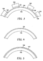
FIG. 3 is a partial illustration of a patterned roll; -
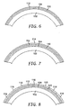
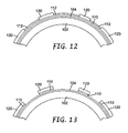
FIGS. 4-13 demonstrate an illustrative but non-limiting method of forming the patterned roll ofFIG. 3 in accordance with an embodiment of the disclosure; -
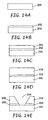
FIGS.14A-14E demonstrate an illustrative but non-limiting method of forming a patterned roll in accordance with an embodiment of the disclosure; -
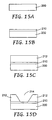
FIGS.15A-15D demonstrate an illustrative but non-limiting method of forming a patterned roll in accordance with an embodiment of the disclosure; -
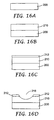
FIGS.16A-16D demonstrate an illustrative but non-limiting method of forming a patterned roll in accordance with an embodiment of the disclosure; -
FIGS.17A-17C demonstrate an illustrative but non-limiting method of forming a patterned roll in accordance with an embodiment of the disclosure; -
FIGS. 18A-18C demonstrate an illustrative but non-limiting method of forming a patterned roll in accordance with an embodiment of the disclosure; -
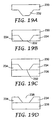
FIGS.19A-19D demonstrate an illustrative but non-limiting method of forming a patterned roll in accordance with an embodiment of the disclosure; -
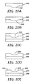
FIGS. 20A-20E demonstrate an illustrative but non-limiting method of forming a patterned roll in accordance with an embodiment of the disclosure; -
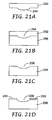
FIGS. 21A-21D demonstrate an illustrative but non-limiting method of forming a patterned roll in accordance with an embodiment of the disclosure; -
FIG. 22 is a perspective view of a microreplication assembly; -
FIG. 23 is a perspective view of a portion of the microreplication assembly ofFIG. 22 ; -
FIG. 24 is a perspective view of a portion of the microreplication assembly ofFIG. 22 ; -
FIG. 25 is a schematic illustration of a roll mounting arrangement; -
FIG. 26 is a schematic illustration of a mounting arrangement for a pair of patterned roll; -
FIG. 27 is a schematic illustration of a motor and roll arrangement to accordance; -
FIG. 28 is a schematic illustration of structure for controlling the registration between rolls; -
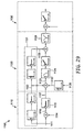
FIG. 29 is a schematic illustration of a control algorithm for controlling registration; and -
FIG. 30 is a diagrammatic cross-sectional view of an article made in accordance with an embodiment of the disclosure; - While the disclosure is amenable to various modifications and alternative forms, specifics thereof have been shown by way of example in the drawings and will be described in detail. It should be understood, however, that the intention is not to limit the disclosure to the particular embodiments described. On the contrary, the intention is to cover all modifications, equivalents, and alternatives falling within the scope of the disclosure:
- The casting assembly and apparatus described below do not fall under the wording of the claims.
- Generally, the present disclosure pertains to producing two-sided microreplicated structures having a first microreplicated pattern on a first surface of a web and a second microreplicated pattern on a second surface of the web. The system generally includes a first patterning assembly and a second patterning assembly. Each respective assembly creates a microreplicated pattern on either a first or second surface of the web. A first pattern can be created on the first surface of the web and a second pattern can be created on the second surface of the web.
- In some instances, the apparatus and methods discussed herein result in a web having a microreplicated structure on each opposing surface of the web that can be manufactured by continuously forming microreplicated structures on opposite surfaces of the web while keeping the microreplicated structures registered generally to within 100 micrometers of each other. In some instances, the microreplicated structures may remain registered within 50 micrometers. In some cases, the microreplicated structures may remain registered within 20 micrometers. In some instances, the microreplicated structures may remain registered within 10 micrometers or even within 5 micrometers.
- The following description should be read with reference to the drawings, in which like elements in different drawings are numbered in like fashion. The drawings, which are not necessarily to scale, depict selected embodiments and are not intended to limit the scope of the disclosure. Although examples of construction, dimensions, and materials are illustrated for the various elements, those skilled in the art will recognize that many of the examples provided have suitable alternatives that may be utilized.
-
FIG.1 illustrates anexample casting apparatus 10 for producing a two-sided web 12 that includes registered microreplicated structures on opposing surfaces. In some instances, thecasting apparatus 10 includes first and second coating means 16, 20, anip roller 14, and first and second patterned rolls 18, 24. In some instances, first coating means 16 may be a first extrusion die 16 while second coating means may be a second extrusion die 20. In the illustrated embodiment, the first and second curable liquid is disposed on the web surface prior to passing through the first and second patterned rolls, respectively. In other embodiments, the first curable liquid is disposed on the first patterned roll and the second curable liquid is disposed on the second patterned roll, which is then transferred to the web from the patterned rolls. -
Web 12 may be presented to the first extrusion die 16, which dispenses a first curableliquid layer coating 22 onto theweb 12. Niproller 14 presses first coating 22 into the first patternedroller 18. In some cases, niproller 14 can be a rubber covered roller. While on the firstpatterned roll 18, thecoating 22 is cured using anenergy source 26 adapted to provide suitable curing energy. In some instances,energy source 26 may be adapted to provide ultraviolet light. The term "ultraviolet light" refers to light having a wavelength in a range from 200 to 500 nanometers or from 200 to 400 nanometers. - A second
curable liquid layer 28 is coated on the opposite side of theweb 12 using a second side extrusion die 20. Thesecond layer 28 is pressed into the secondpatterned tool roller 24 and the curing process repeated for thesecond coating layer 28. Registration of the two coating patterns is achieved by maintaining thetool rollers -
FIG. 2 provides a closer view at first and second patterned rolls 44 and 46. First and second patterned rolls 44, 46 may be considered as particular embodiments of patternedrolls FIG. 1 . Other patterns are contemplated, as will be discussed in greater detail subsequently. First patternedroll 44 has afirst pattern 42 for forming a microreplicated surface. Second pattern roll 46 has a secondmicroreplicated pattern 50. In the illustrated embodiment, first andsecond patterns - As a
web 30 passes over the firstpatterned roll 44, a first curable liquid (not shown) on afirst surface 32 may be cured by curing energy provided by anenergy source 34 near afirst region 36 on the firstpatterned roll 44. A first microreplicatedpatterned structure 54 is formed on the first side 43 of theweb 30 after the liquid is cured. The firstpatterned structure 54 is a negative of thepattern 42 on the firstpatterned roll 44. After the firstpatterned structure 54 is formed, a secondcurable liquid 52 is dispensed onto asecond surface 38 of theweb 30. To insure that thesecond liquid 52 is not cured prematurely, thesecond liquid 52 is isolated from thefirst energy source 34, typically by locating thefirst energy source 34 so that energy emitted by thefirst energy source 34 does not fall on thesecond liquid 52. If desired, the curing sources can be located inside their respective patterned rolls. As such, the opaque nature ofweb 30 can aid in preventing undesired curing. - After the first
patterned structure 54 is formed, theweb 30 continues along thefirst roll 44 until it enters agap region 48 between the first and second patterned rolls 44, 46. The second liquid 52 then engages thesecond pattern 50 on the secondpatterned roll 46 and is shaped into a second microreplicated structure, which is then cured by curing energy emitted by asecond energy source 40. As theweb 30 passes into thegap 48 between first and second patterned rolls 44, 46, the first patterned structured 54, which is by this time substantially cured and bonded to theweb 30, restrains theweb 30 from slipping while theweb 30 begins moving into thegap 48 and around the second patternedroller 46. This removes web stretching and slippages as a source of registration error between the first and second patterned structures formed on the web. - By supporting the
web 30 on the firstpatterned roll 44 while thesecond liquid 52 comes into contact with the secondpatterned roll 46, the degree of registration between the first and secondmicroreplicated structures opposite sides web 30 becomes a function of controlling the positional relationship between the surfaces of the first and second patterned rolls 44, 46. The S-wrap of the web around the first and second patterned rolls 44, 46 and between thegap 48 formed by the rolls minimizes effects of tension, web strain changes, temperature, microslip caused by mechanics of nipping a web, and lateral position control. The S-wrap can maintain theweb 30 in contact with each roll over a wrap angle of 180 degrees, though the wrap angle can be more or less depending on the particular requirements. - In some instances, it may be useful to provide microreplicated patterns onto either side of a flexible web or substrate that is opaque, particularly, opaque to curing energy. In other instances, it may be useful to provide microreplicated patterns onto either side of a flexible web or substrate that is transparent, particularly, transparent to curing energy. When the web or substrate is opaque to the curing energy necessary to cure the materials applied to the web in liquid form, the materials cannot simply be cured by passing curing energy through the web or substrate to contact the liquid resin. In these cases, it may be useful to use a patterned roll that is transparent to a particular curing energy or includes portions that are transparent to curing energy. In some cases, only one patterned roll is transparent.
-
FIG. 3 is a partial illustration of an illustrative but non-limiting patterned roll and should not be considered as being to scale. Instead, the pattern has been exaggerated for clarity. Patterned roll can, as illustrated and as will be discussed in greater detail, may be formed by an additive method in which materials are deposited onto the surface of a transparent cylinder or other suitable shape. In some embodiments, it is believed that patterned roll may be formed using various subtractive methods in which material is removed from a transparent cylinder or other suitable shape. - Patterned roll includes a
transparent cylinder 102 that can be formed of any suitable material. In some instances,transparent cylinder 102 is formed of a material that is transparent to the curing energy that will cure the curable material that will be applied to patterned, roll. In some instances, as illustrated,transparent cylinder 102 can be made from a glass such as quartz. - As illustrated, in particular, patterned roll includes a
quartz cylinder 102.Quartz cylinder 102 may be of any suitable dimensions, although in somecases quartz cylinder 102 may have a length of 3 inches and a radius of 3 inches.Quartz cylinder 102 may be a substantially solid cylinder, or, as illustrated,quartz cylinder 102 may be a hollow cylinder. - In some cases, it may be useful to apply a
thin tie layer 104 to the surface of thequartz cylinder 102. This may assist subsequent materials in adhering or bonding to the quartz. In some instances,tie layer 104 is thin enough to not materially change the optical properties of thequartz cylinder 102. At a minimum,tie layer 104 can be thin enough to remain transparent to curing energy.Tie layer 104 may be formed of any suitable material and using any suitable application technique. In some instances,tie layer 104 includes or consists of titanium and is applied via sputtering. - Once
tie layer 104 has been formed, subsequent materials may be added to patterned roll. While particular processing steps are illustrated inFIGS. 4-13 , and will be discussed in detail with respect to the Example, a variety of opaque materials may be applied to tielayer 104. Suitable opaque materials include metals such as chrome, copper or aluminum, and curable polymers such as silicone and epoxy. Suitable materials may be applied and patterned using any suitable technique, such as sputtering, etching, and the like. - In the illustrated embodiment, the features of patterned roll have been formed in two steps. First, layers 106 have been deposited onto
tie layer 104 and subsequently patterned.Layers 108 have been formed and patterned on top oflayers 106.Layers 106 andlayers 108 may be formed of different materials or they may be formed of the same material. In some instances,layers 106 may be formed by sputtering a layer of chrome ontotie layer 104. In some instances,layers 108 may be formed by plating chrome ontolayers 106. - In
FIG. 3 , the opaque features of patterned roll stand above the surface ofquartz cylinder 102. In some contemplated embodiments, such as those discussed with respect toFIGS. 14-21 , the opaque features are actually closer to an outer surface of the substrate, while the transparent features actually penetrate the substrate. In either event, the opaque features may be considered as being farther from a radial center of patterned roll than are the transparent features. - In some instances, a patterned roll may be formed from either machinable or non-machinable transparent substrates. Several contemplated manufacturing techniques are described herein in
Figs. 14-21 . It should be noted that inFIGS.14-21 , only a very small part of a transparent substrate is shown, for ease of illustration. While only a single transparent feature is shown for each potential manufacturing technique, it should be noted that of course a patterned roll will include a number of features. Moreover, it should be noted that a patterned roll will be cylindrical, while for ease of illustration and because only a very small part of the roll is shown,FIGS. 14-21 appear rectangular. -
FIGS. 14A-14E illustrate a potential method of forming opaque features on a non-machinable transparent substrate that includes adding a machinable layer. InFIG. 14A, a non-machinable, transparent,substrate 200 is provided. Examples of non-machinable, transparent substrates include glasses such as quartz. As shown inFIG. 14B , atitanium tie layer 202 may be applied tosubstrate 200 using any suitable technique such as sputtering. Acopper seed layer 204 may be sputtered ontotitanium tie layer 202 as seen inFIG.14C . Additional copper may be plated ontocopper seed layer 204 to formcopper layer 206, as seen inFIG. 14D . -
FIG.14E shows thatcopper layer 206 could be machined in any suitable manner to provide atransparent feature 208 positioned withincopper layer 206, which is of course opaque. In some instances,transparent feature 208 could be formed simply by a machining process such as micromilling, laser ablation, diamond turning or EDM processing. In some cases, additional processing such as a brief chemical etch may be useful in exposingtransparent substrate 200 without damagingtransparent substrate 200. - In some instances, other materials may be used for the
machinable layer 206. For example,machinable layer 206 could be formed from an opaque epoxy or a machinable ceramic that could be coated in a "green" state and sintered after shaping. -
FIGS. 15A-15D illustrate another potential method of forming opaque features on a non-machinabletransparent substrate 200 that includes adding a machinable layer. InFIG.15B , atransparent epoxy layer 210 may be added to thetransparent substrate 200 to help protect the transparent substrate during subsequent machining. As seen inFIG. 15C , anopaque epoxy layer 212 has been added on top of thetransparent epoxy layer 210. InFIG. 15D ,opaque epoxy layer 212 has been machined using any suitable technique to formtransparent feature 214. -
FIGS. 16A-D illustrate another potential method of forming opaque features on a non-machinabletransparent substrate 200 that includes adding a machinable layer.Transparent substrate 200 is shown inFIG. 16A . InFIG. 16B , a relatively thickertransparent epoxy layer 210 has been added atoptransparent substrate 200. A relatively thinneropaque epoxy layer 212 has been added ontransparent epoxy layer 210 as shown inFIG. 16C . InFIG. 16D , theopaque epoxy layer 212 and thetransparent epoxy layer 210 have been machined using any suitable technique to formtransparent feature 216. As an alternate, it may be feasible to machinetransparent feature 216 into a transparent epoxy layer, then coat the tops of the transparent epoxy layer with an opaque epoxy layer. -
FIGS. 17A-17C illustrate a potential method of forming opaque features on a machinable transparent substrate.FIG. 17A shows a machinabletransparent substrate 220 that can be formed of a machinable transparent polymer. In some instances,substrate 220 can be formed from PMMA (poly methyl methacrylate). InFIG.17B , anopaque coating 222 such as sputtered aluminum or copper has been added ontotransparent substrate 220. Alternatively, it is contemplated thatopaque coating 222 could also be formed from an opaque epoxy or even an opaque filled epoxy. As shown inFIG.17C , atransparent feature 224 can be formed using any suitable machining technique. -
FIGS.18A-C illustrate another potential method of forming opaque features on machinabletransparent substrate 220. InFIG.18B ,transparent substrate 220 has been machined using any suitable technique to formtransparent feature 226. Subsequently, as shown inFIG.18C , the portions oftransparent substrate 220 beyondtransparent feature 226 may coated with anopaque coating 228. -
FIGS. 19A-19D illustrate a potential method of using a separately-created master mold to replicate raised features on a transparent substrate. The raised features can then be coated to be opaque. InFIG. 19A , amaster mold 230 can be cut from any suitable material using standard precision machining techniques.Master mold 230 can be seen to includeprotrusion 232, which will ultimately form a transparent feature. - As seen in
FIG.19B ,master mold 230 can be filled with anopaque epoxy material 234 and then is applied to the surface of a desiredsubstrate 236 such as quartz or PMMA as seen inFIG.19C . The epoxy can be allowed to cure, and thenmaster mold 230 may be removed, as seen inFIG. 19D , leavingsubstrate 236 having atransparent feature 238 with anopaque layer 234 on either side of thetransparent feature 238. -
FIGS. 20A-20E illustrate another potential method of using a separately-created master mold to replicate raised features on a transparent substrate. The raised features can then be coated to be opaque. InFIG. 20A , amaster mold 240 can be cut from any suitable material using standard precision machining techniques.Master mold 240 can be seen to includeprotrusion 242, which will ultimately form a transparent feature. - As seen in
FIG. 20B ,master mold 240 can be filled with a transparentepoxy material 244 and then is applied to the surface of a desiredsubstrate 246 such as quartz or PUMA as seen inFIG. 20C . The epoxy can be allowed to cure, and thenmaster mold 240 may be removed, as seen inFIG. 20D , leavingsubstrate 246 having atransparent feature 248. As seen inFIG. 20E , anopaque epoxy layer 250 can be applied totransparent epoxy layer 244 on either side of thetransparent feature 248. -
FIGS. 21A-21D illustrate another potential method of using a separately-created master mold to replicate raised features on a transparent substrate. The raised features can then be coated to be opaque. InFIG. 21A , amaster mold 252 can be cut from any suitable material using standard precision machining techniques.Master mold 252 can be seen to includeprotrusion 254, which will ultimately form a transparent feature. - As seen in
FIG. 21B ,master mold 252 has been imprinted directly into a machinabletransparent substrate 256. InFIG. 21C ,master mold 252 has been removed, leavingtransparent substrate 256 includingtransparent feature 258. As shown inFIG. 21D ,transparent substrate 256 can be coated with anopaque epoxy layer 258 on either side oftransparent feature 258. - Referring now to
FIGS. 22-23 , an example embodiment of asystem 110 including a roll to rollcasting apparatus 120 is illustrated. In the depictedcasting apparatus 120, a web 122 is provided to thecasting apparatus 120 from a main unwind spool (not shown). The exact nature of web 122 can vary widely, depending on the product being produced. However, thecasting apparatus 120 is capable of handling a web 122 that is both flexible and transparent and/or opaque, as discussed previously. The web 122 is directed around various rollers 126 into thecasting apparatus 120. - Accurate tension control of the web 122 is beneficial in achieving optimal results, so the web 122 may be directed over a tension-sensing device (not illustrated). If an optional liner web is used to protect the web 122, the liner web (not illustrated) can be separated at the unwind spool and directed onto a liner web wind-up spool (not shown). The web 122 can be directed via an idler roll to a dancer roller for precision tension control. Idler rollers can direct the web 122 to a position between nip roller 154 and first coating head 156.
- A variety of coating methods may be employed. In some embodiments, as illustrated, first coating head 156 is a die coating head. The web 122 then passes between the nip roll 154 and first patterned roll 160. The first patterned roll 160 has a patterned surface 162, and when the web 122 passes between the nip roller 154 and the first patterned roll 160 the material dispensed onto the web 122 by the first coating head 156 is shaped into a negative of patterned surface 162.
- While the web 122 is in contact with the first patterned roll 160, material is dispensed from second coating head 164 onto the other surface of web 122. In parallel with the discussion above with respect to the first coating head 156, the second coating head 164 is also a die coating arrangement including a second extruder (not shown) and a second coating die (not shown). In some embodiments, the material dispensed by the first coating head 156 is a composition including a polymer precursor and intended to be cured to solid polymer with the application of curing energy such as ultraviolet radiation.
- Material that has been dispensed onto web 122 by the second coating head 164 is then brought into contact with second patterned roll 174 with a second patterned surface 176. In parallel with the discussion above, in some embodiments, the material dispensed by the second coating head 164 is a composition including a polymer precursor and intended to be cured to solid polymer with the application of curing energy such as ultraviolet radiation.
- At this point, the web 122 has had a pattern applied to both sides. A peel roll 182 may be present to assist in removal of the web 122 from second patterned roll 174. In some instances, the web tension into and out of the casting apparatus is nearly constant.
- The web 122 having a two-sided microreplicated pattern is then directed to a wind-up spool (not shown) via various idler rolls. If an interleave film is desired to protect web 122, it may be provided from a secondary unwind spool (not shown) and the web and interleave film are wound together on the wind-up spool at an appropriate tension.
- Referring to
FIGS. 22-24 , first and second patterned rolls are coupled to first andsecond motor assemblies motor assemblies frame 230, either directly or indirectly. Themotor assemblies first motor assembly 210 is fixedly mounted toframe 230.Second motor assembly 220, which is placed into position when web 122 is threaded through thecasting apparatus 120, may need to be positioned repeatedly and therefore can be movable, both in the cross- and machine direction.Movable motor arrangement 220 may be coupled tolinear slides 222 to assist in repeated accurate positioning, for example, when switching between patterns on the rolls.Second motor arrangement 220 also includes a second mounting arrangement 225 on the backside of theframe 230 for positioning the second patterned roll 174 side-to-side relative to the first patterned roll 160. In some cases, second mounting arrangement 225 includes linear slides 223 allowing accurate positioning in the cross machine directions. - Referring to
FIG. 25 , a motor mounting arrangement is illustrated. Amotor 633 for driving a tool or patternedroll 662 is mounted to themachine frame 650 and connected through acoupling 640 to arotating shaft 601 of the patternedroller 662. Themotor 633 is coupled to aprimary encoder 630. A secondary encoder 651 is coupled to the tool to provide precise angular registration control of the patternedroll 662. Primary 630 and secondary 651 encoders cooperate to provide control of the patternedroll 662 to keep it in registration with a second patterned roll, as will be described further hereinafter. - Reduction or elimination of shaft resonance is important as this is a source of registration error allowing pattern position control within the specified limits. Using a
coupling 640 between themotor 633 andshaft 650 that is larger than general sizing schedules specify will also reduce shaft resonance caused by more flexible couplings.Bearing assemblies 660 are located in various locations to provide rotational support for the motor arrangement. - In the example embodiment shown, the
tool roller 662 diameter can be smaller than itsmotor 633 diameter. To accommodate this arrangement, tool rollers may be installed in pairs, arranged in mirror image. InFIG. 26 , twotool roller assemblies tool rollers FIG. 22 , the first motor arrangement is typically fixedly attached to the frame and the second motor arrangement is positioned using movable optical quality linear slides. -
Tool roller assembly 710 is quite similar totool roller assembly 610, and includes amotor 733 for driving a tool or patternedroll 762 is mounted to themachine frame 750 and connected through acoupling 740 to a rotating shaft 701 of the patternedroller 762. Themotor 733 is coupled to aprimary encoder 730. Asecondary encoder 751 is coupled to the tool to provide precise angular registration control of the patternedroll 762. Primary 730 and secondary 751 encoders cooperate to provide control of the patternedroll 762 to keep it in registration with a second patterned roll, as will be described further hereinafter. - Reduction or elimination of shaft resonance is important as this is a source of registration error allowing pattern position control within the specified limits. Using a
coupling 740 between themotor 733 andshaft 750 that is larger than general sizing schedules specify will also reduce shaft resonance caused by more flexible couplings.Bearing assemblies 760 are located in various locations to provide rotational support for the motor arrangement. - Because the feature sizes on the microreplicated structures on both surfaces of a web are desired to be within fine registration of one another, the patterned rolls should be controlled with a high degree of precision. Cross-web registration within the limits described herein can be accomplished by applying the techniques used in controlling machine-direction registration, as described hereinafter.
- For example, to achieve about 10 micrometers end-to-end feature placement on a 10-inch circumference patterned roller, each roller must be maintained within a rotational accuracy of ± 32 arc-seconds per revolution. Control of registration becomes more difficult as the speed the web travels through the system is increased.
- Applicants have built and demonstrated a system having 10-inch circular patterned rolls that can create a web having patterned features on opposite surfaces of the web that are registered to within 2.5 micrometers. Upon reading this disclosure and applying the principles taught herein, one of ordinary skill in the art will appreciate how to accomplish the degree of registration for other microreplicated surfaces.
- Referring to
FIG. 27 , a schematic of amotor arrangement 800 is illustrated.Motor arrangement 800 includes amotor 810 including aprimary encoder 830 and adrive shaft 820. Driveshaft 820 is coupled to a drivenshaft 840 of patternedroll 860 through acoupling 825. A secondary, or load,encoder 850 is coupled to the drivenshaft 840. Using two encoders in the motor arrangement described allows the position of the patterned roll to be measured more accurately by locating the measuring device (encoder) 850 near the patternedroll 860, thus reducing or eliminating effects of torque disturbances when themotor arrangement 800 is operating. - Referring to
FIG. 28 , a schematic of the motor arrangement ofFIG. 27 , is illustrated as attached to control components. In the example apparatus shown inFIGS. 1-3 , a similar set-up would control eachmotor arrangement motor arrangement 900 includes amotor 910 including aprimary encoder 930 and adrive shaft 920. Driveshaft 920 is coupled to a drivenshaft 940 of patternedroll 960 through acoupling 930. A secondary, or load,encoder 950 is coupled to the drivenshaft 940. -
Motor arrangement 900 communicates with acontrol arrangement 965 to allow precision control of the patternedroll 960.Control arrangement 965 includes adrive module 966 and aprogram module 975. Theprogram module 975 communicates with thedrive module 966 via aline 977, for example, a SERCOS fiber network. Theprogram module 975 is used to input parameters, such as set points, to thedrive module 966.Drive module 966 receives input 480 volt, 3-phase power 915, rectifies it to DC, and distributes it via apower connection 973 to control themotor 910.Motor encoder 912 feeds a position signal to controlmodule 966 vialine 972. Thesecondary encoder 950 on the patternedroll 960 also feeds a position signal back to thedrive module 966 via toline 971. Thedrive module 966 uses the encoder signals to precisely position the patternedroll 960. The control design to achieve the degree of registration is described in detail below. - In the illustrative embodiments shown, each patterned roll is controlled by a dedicated control arrangement. Dedicated control arrangements cooperate to control the registration between first and second patterned rolls. Each drive module communicates with and controls its respective motor assembly.
- The control arrangement in the system built and demonstrated by Applicants include the following. To drive each of the patterned rolls, a high performance, low cogging torque motor with a high-resolution sine encoder feedback (512 sine cycles x 4096 drive interpolation >> 2 million parts per revolution) was used, model MHD090B-035 NGO-LTN, available from Bosch-Rexroth (Indramat). Also the system included synchronous motors, model MHD090B-035-NGO-UN, available from Bosch-Rexroth (Indramat), but other types, such as induction motors could also be used.
- Each motor was directly coupled (without gearbox or mechanical reduction) through an extremely stiff bellows coupling, model BK5-300, available from R/W Corporation. Alternate coupling designs could be used, but bellows style generally combines stiffness while providing high rotational accuracy. Each coupling was sized so that a substantially larger coupling was selected than what the typical manufacturers specifications would recommend.
- Additionally, zero backlash collets or compressive style locking hubs between coupling and shafts are preferred. Each roller shaft was attached to an encoder through a hollow shaft load side encoder, model RON255C, available from Heidenhain Corp., Schaumburg, IL. Encoder selection should have the highest accuracy and resolution possible, typically greater than 32 arc-sec accuracy. Applicants' design, 18000 sine cycles per revolution were employed, which in conjunction with the 4096 bit resolution drive interpolation resulted in excess of 50 million parts per revolution resolution giving a resolution substantially higher than accuracy. The load side encoder had an accuracy of +/- 2 arc-sec; maximum deviation in the delivered units was less than +/- 1 arc-sec.
- In some instances, each shaft may be designed to be as large a diameter as possible and as short as possible to maximize stiffness, resulting in the highest possible resonant frequency. Precision alignment of all rotational components is desired to ensure minimum registration error due to this source of registration error.
- Referring to
FIG. 29 , identical position reference commands were presented to each axis simultaneously through a SERCOS fiber network at a 2 ms update rate. Each axis interpolates the position reference with a cubic spline, at the position loop update rate of 250 microsecond intervals. The interpolation method is not critical, as the constant velocity results in a simple constant times time interval path. The resolution is critical to eliminate any round off or numerical representation errors. Axis rollover is also addressed. In some cases, it is important that each axis' control cycle is synchronized at the current loop execution rate (62 microsecond intervals). - The
top path 1151 is the feed forward section of control. The control strategy includes aposition loop 1110, avelocity loop 1120, and acurrent loop 1130. Theposition reference 1111 is differentiated, once to generate the velocity feed forward terms 1152 and a second time to generate the acceleration feedforward term 1155. Thefeed forward path 1151 helps performance during line speed changes and dynamic correction. - The
position command 1111 is subtracted fromcurrent position 1114, generating anerror signal 1116. Theerror 1116 is applied to aproportional controller 1115, generating thevelocity command reference 1117. Thevelocity feedback 1167 is subtracted from thecommand 1117 to generate thevelocity error signal 1123, which is then applied to a PID controller. Thevelocity feedback 1167 is generated by differentiating the motorencoder position signal 1126. Due to differentiation and numerical resolution limits, a lowpass Butterworth filter 1124 is applied to remove high frequency noise components from theerror signal 1123. A narrow stop band (notch)filter 1129 is applied at the center of the motor - roller resonant frequency. This allows substantially higher gains to be applied to thevelocity controller 1120. Increased resolution of the motor encoder also would improve performance. The exact location of the filters in the control diagram is not critical; either the forward or reverse path are acceptable, although tuning parameters are dependent on the location. - A PID controller could also be used in the position loop, but the additional phase lag of the integrator makes stabilization more difficult. The current loop is a traditional PI controller; gains are established by the motor parameters. The highest bandwidth current loop possible will allow optimum performance. Also, minimum torque ripple is desired.
- Minimization of external disturbances is important to obtaining maximum registration. This includes motor construction and current loop commutation as previously discussed, but minimizing mechanical disturbances is also important. Examples include extremely smooth tension control in entering and exiting web span, uniform bearing and seal drag, minimizing tension upsets from web peel off from the roller, uniform rubber nip roller. In the current design a third axis geared to the tool rolls is provided as a pull roll to assist in removing the cured structure from the tool.
- The web material can be any suitable material on which a microreplicated patterned structure can be created. A number of different materials may be used, depending on the ultimate use of the microreplicated patterned structure. If, for example, the microreplicated patterned structure will form a flexible circuit board, the web material may be a metallized polymeric film such as metallized KAPTON.
- The liquid from which the microreplicated structures are created can be a curable photocurable material, such as acrylates curable by UV light. One of ordinary skill in the art will appreciate that other coating materials can be used, for example, polymerizable material, and selection of a material will depend on the particular characteristics desired for the microreplicated structures. For example, if a flexible circuit board is being made, the coating material may include a conductive or insulating polymer. In some embodiments, the coating material includes an electroplate masking material and/or nonconductive or insulating polymers.
- Examples of coating means that useful for delivering and controlling liquid to the web or patterned roll are, for example, die or knife coating, coupled with any suitable pump such as a syringe or peristaltic pump. One of ordinary skill in the art will appreciate that other coating means can be used, and selection of a particular means will depend on the particular characteristics of the liquid to be delivered to the web or patterned roll.
- Examples of curing energy sources are infrared radiation, ultraviolet radiation, visible light radiation, or microwave. One of ordinary skill in the art will appreciate that other curing sources can be used, and selection of a particular web material/curing source combination will depend on the particular article (having microreplicated structures in registration) to be created.
-
FIG. 30 schematically illustrates a contemplated coatedmicroreplicated article 1200 formed according to the methods and using the apparatus described herein.Article 1200 includes a flexibleopaque web 1202 and a number of schematic elements disposed on either side ofopaque web 1202.Element 1204 is disposedopposite element 1206. Similarly,element 1208,element 1212 andelement 1216 are disposedopposite element 1210,element 1214 andelement 1218, respectively. It should be noted that these elements can be considered as generically representing a number of different potential elements. These elements may be circuitry, for example. In some embodiments, the microreplicated pattern includes an electroplate mask that can pass through an additive circuit plating step. - In some embodiments, such as that illustrated, there may be little or no lands between adjacent elements. For example, there may be little or no coated material remaining on
opaque web 1202 betweenelement 1204 andelement 1208. This may have advantages if, for example, the coated material is an electrically conductive material or an electroplate mask. In some embodiments, an additional washing step can remove uncured material from the microreplicated pattern to produce a microreplicated features having no land areas and separated from one another. In other instances,article 1202 may include lands, i.e. coated material-remaining onopaque web 1202 between adjacent elements. -
FIGS. 4-13 illustrate an additive process for forming a patterned roll much like patterned roll ofFIG. 3 . Quartz tubes 3 inches long and 3 inches in radius were cleaned with water, acetone and methyl ethyl ketone (MEK), and were then placed under a UV lamp for 15 minutes. The quartz tubes were then mounted on a rotating table in a high vacuum sputter chamber, and the pressure within the chamber was slowly reduced to 1 x 10⁻⁶ Torr over a period of one hour. A strip of chrome plated steel previously mounted within the chamber was electrically connected to an arc welder. The arc welder passed a current through the metal strip and the metal strip was thus heated to red hot. The rotating quartz tubes were washed by the resulting IR radiation for 10 minutes. - Once the quartz tubes were cleaned, a
quartz cylinder 102 as seen inFIG. 4 was sputtered with athin layer 104 of chrome, which acts as an adhesion layer between the quartz and the nickel layer to follow. - Next, and as shown schematically in
FIG. 5 , anickel metallization layer 110 was sputtered onto thechrome tie layer 104. - Next, and as shown schematically in
FIG. 6 , aprotective copper layer 112 was applied over thenickel metallization layer 110. Thecopper layer 112 was a sacrificial layer that was intended to protect thenickel layer 110 from contamination and oxidation during subsequent processing steps. - Next, and as shown schematically in
FIG. 7 , a photoresist (SC Resists, Arch Semiconductor Photopolymers Company)layer 114 has been added on top of thecopper layer 112. The height of thephotoresist layer 114 ultimately sets the height of the features being formed onquartz cylinder 102. In the Example, thephotoresist layer 114 was formed to be 50 micrometers thick, and was softbaked at 115 degrees Celsius for 30 seconds prior to exposure. - Next, and as shown schematically in
FIG. 8 , thephotoresist layer 114 was patterned by shining light in a desired pattern onto thephotoresist layer 114. Consequently, thephotoresist layer 114 now hasportions 116 that will remain, andportions 118 that will be removed after developing. - Next, and as shown schematically in
FIG. 9 , the photoresist was developed. After sitting for at least 30 minutes, the photoresist was subjected to a post exposure bake at 115 degrees Celsius for 1 minute. The photoresist was then developed via exposure to developing solution for 30 to 60 seconds. Consequently, resistportions 116 remain oncopper layer 112 while resistportions 118 have been removed. - Next, and as shown schematically in
FIG.10 , the exposed portions ofcopper layer 112 were removed in an etching process. Sodium persulfate was used to remove the exposed copper because sodium persulfate reacts quickly with copper but slowly with the chrome underlying the copper, as it is desirable to keep the chrome layer as thick as possible. - Next, and as shown schematically in
FIG.11 ,chrome sections 120 were plated onto the freshly exposedchrome layer 110, in between resistregions 116.Chrome sections 120 were plated using low current densities on the order of 1mA/17mm2. As the current density increases, even at levels as low as 20mA/17mm2, either internal stress was high, causing the chrome to peel off, or severe pitting occurred. The geometry ofchrome sections 120 were determined by resistregions 116. - Next, and as shown schematically in
FIG. 12 , the remaining cured photoresist, in resistregions 116, were removed using a basic solution. Finally, and as shown schematically inFIG. 13 , the remainingcopper layer 112 was removed using a sodium persulfate bath as discussed above. The resulting patterned roll has opaque regions corresponding tonickel 110 andchrome sections 120, and transparent regions corresponding to wheretie layer 104 is not covered by opaque material. - The disclosure should not be considered limited to the particular examples described above, but rather should be understood to cover all aspects of the disclosure as set out in the attached claims. Various modifications, equivalent processes, as well as numerous structures to which the disclosure can be applicable will be readily apparent to those of skill in the art upon review of the instant specification.
Claims (23)
- A microreplicated article comprising: ..
a flexible opaque substrate having a first surface and a second surface;
a first coated microreplicated pattern on the first surface; and
a second coated microreplicated pattern on the second surface, wherein the first and second patterns are registered to within 100 micrometers; wherein the flexible opaque substrate is opaque to the energy employed for curing the first and second microreplicated patterns. - The article of claim 1, wherein the first and second patterns are registered to within 10 micrometers.
- The article of claim 1, wherein the first and second patterns are registered to within 5 micrometers.
- The article of claims 1 to 3, wherein the flexible opaque substrate is opaque to ultraviolet light.
- The article of claim 4, wherein the flexible opaque substrate blocks at least 98 percent of ultraviolet light that is incident upon the flexible opaque substrate.
- The article of claims 1 to 5, wherein the flexible opaque substrate comprises polymer suitable for forming a flexible circuit board.
- The article of claim 6, wherein the flexible opaque substrate comprises a metallized polymer.
- The article of claims 1 to 7, wherein the first coated microreplicated pattern comprises a photocurable polymer.
- The article of claims 1 to 8, wherein the second coated microreplicated pattern comprises a photocurable polymer.
- The article of claims 1 to 9, wherein the first coated microreplicated pattern comprises a plurality of distinct elements, and at least some of the distinct elements are discontinuous from other distinct elements.
- The article of claims 1 to 10, wherein the second coated microreplicated pattern comprises a plurality of distinct elements, and at least some of me distinct elements are discontinuous from other distinct clement.
- A method of making a microreplicated article including an opaque web having a first surface and an opposing second surface, the method comprising:passing an opaque web having a first surface and an opposing second surface through a casting apparatus having a first patterned roll and a second patterned roll;contacting a first liquid with the first patterned roll and the first surface;curing the first liquid to create a first microreplicated pattern;contacting a second liquid with the second patterned roll and the second surface while the first microreplicated pattern is in contact with the first pattern roll; andcuring the second liquid to create a second microreplicated pattern, wherein the first and second patterns are registered to within 100 micrometers; wherein the opaque web is opaque to a curing energy used for curing the first and/or second liquid.
- The method of claim 12, wherein contacting the first liquid comprises contacting a photocurable acrylate resin with the first patterned roll and the first surface.
- The method of claims 12 or 13, wherein contacting the second liquid comprises contacting a photocurable acrylate resin with the second patterned roll and the second surface.
- The method of claims 12 to 14, wherein contacting the first liquid comprises contacting a photocurable insulating polymer with the first patterned roll and the first surface.
- The method of claims 12 to 15, wherein contacting the second liquid comprises contacting a photocurable insulating polymer with the second patterned roll and the second surface.
- A method of making a microreplicated article comprising an opaque web having a first side and an opposing second side, the method comprising steps of:disposing curable material onto a web having a first side and an opposing second side, or onto a first patterned roll and second patterned roll;directing the opaque web into contact with the first patterned roll, the first patterned roll comprising a first plurality of opaque regions disposed on a transparent substrate;curing the curable material on the first side of the web to form a first microreplicated pattern;directing the opaque web into contact with the second patterned roll, the second patterned roll comprising a second plurality of opaque regions disposed on a transparent substrates; andcuring the curable material on the second side of the web to form a second microreplicated pattern;wherein the first and second sides of the web are patterned while the web is in continuous motion such that the first and second patterns are maintained in continuous registration to within 100 micrometers; wherein the opaque web is opaque to a curing energy used to cure the curable material.
- The method of claim 17, wherein the first and second patterns are transferred to first and second sides of the web in registration to within 5 micrometers.
- The method of claim 18, wherein disposing curable material onto the web comprises:disposing curable material onto the first side of the web prior to the first side of the web contacting the first patterned roll; anddisposing curable material onto the second side of the web prior to the second side of the web contacting the second patterned roll.
- The method of claims 18 or 19, wherein disposing curable material onto the first patterned roll and second patterned roll comprises:disposing curable material onto a first patterned roll prior to the first side of the web contacting the first patterned roll; anddisposing curable material onto the second patterned roll prior to the second side of the web contacting the second patterned roll.
- The method of claims 17 to 20, whereon at least a portion of curing the curable material on the first side of the web occurs simultaneously with at least a portion of curing the curable material on the second side of the web.
- The method of claims 17 to 21, wherein curing the curable material on the first side of the web comprises subjecting the curable material to ultraviolet radiation that passes at least partially through the first patterned roll.
- The method of claim 17 to 22, wherein curing the curable material on the second side of the web comprises subjecting the curable material to ultraviolet radiation that passes at least partially through the second patterned roll.
Applications Claiming Priority (2)
| Application Number | Priority Date | Filing Date | Title |
|---|---|---|---|
| US66143105P | 2005-03-09 | 2005-03-09 | |
| PCT/US2006/007975 WO2006098938A1 (en) | 2005-03-09 | 2006-03-06 | Microreplicated article and method for the production thereof |
Publications (2)
| Publication Number | Publication Date |
|---|---|
| EP1855815A1 EP1855815A1 (en) | 2007-11-21 |
| EP1855815B1 true EP1855815B1 (en) | 2011-03-02 |
Family
ID=36571982
Family Applications (1)
| Application Number | Title | Priority Date | Filing Date |
|---|---|---|---|
| EP06737183A Not-in-force EP1855815B1 (en) | 2005-03-09 | 2006-03-06 | Microreplicated article and method for the production thereof |
Country Status (10)
| Country | Link |
|---|---|
| US (1) | US7931841B2 (en) |
| EP (1) | EP1855815B1 (en) |
| JP (1) | JP4988698B2 (en) |
| KR (1) | KR101312140B1 (en) |
| CN (1) | CN101137449B (en) |
| AT (1) | ATE500001T1 (en) |
| BR (1) | BRPI0608701A2 (en) |
| DE (1) | DE602006020416D1 (en) |
| MX (1) | MX2007010907A (en) |
| WO (1) | WO2006098938A1 (en) |
Families Citing this family (20)
| Publication number | Priority date | Publication date | Assignee | Title |
|---|---|---|---|---|
| US7165959B2 (en) * | 2003-09-09 | 2007-01-23 | 3M Innovative Properties Company | Apparatus and method for producing two-sided patterned webs in registration |
| US7804649B2 (en) * | 2003-09-09 | 2010-09-28 | 3M Innovative Properties Company | Microreplicated achromatic lens |
| US7224529B2 (en) * | 2003-09-09 | 2007-05-29 | 3M Innovative Properties Company | Microreplicated article |
| US20050231809A1 (en) * | 2003-09-09 | 2005-10-20 | Carlson Daniel H | Microreplicated polarizing article |
| WO2006098958A1 (en) * | 2005-03-09 | 2006-09-21 | 3M Innovative Properties Company | Microreplicated article with defect-reducing surface |
| US7767273B2 (en) * | 2005-03-09 | 2010-08-03 | 3M Innovative Properties Company | Apparatus and method for producing two-sided patterned web in registration |
| BRPI0609284A2 (en) * | 2005-03-09 | 2010-09-08 | 3M Innovative Properties Co | microreplicated article, method of producing a microreplicated article, and optical monitor |
| EP1874524B1 (en) * | 2005-03-09 | 2009-03-11 | 3M Innovative Properties Company | Apparatus and method for making microreplicated article |
| US7976741B2 (en) * | 2007-02-12 | 2011-07-12 | Ichia Technologies, Inc. | Method of manufacturing light guide plate of keypad |
| US20100252961A1 (en) * | 2009-04-06 | 2010-10-07 | 3M Innovative Properties Company | Optical film replication on low thermal diffusivity tooling with conformal coating |
| WO2011161489A1 (en) | 2010-06-25 | 2011-12-29 | Nokia Corporation | User interfaces and associated apparatus and methods |
| TW201202008A (en) * | 2010-07-12 | 2012-01-16 | Hon Hai Prec Ind Co Ltd | Device and method for making optical film |
| KR20120067163A (en) * | 2010-12-15 | 2012-06-25 | 삼성모바일디스플레이주식회사 | Apparatus for thin layer deposition and method for manufacturing of organic light emitting display apparatus using the same |
| TWI552861B (en) * | 2012-02-08 | 2016-10-11 | 鴻海精密工業股份有限公司 | Apparatus and methods for fabricating a light guide film |
| CN103246006A (en) * | 2012-02-10 | 2013-08-14 | 鸿富锦精密工业(深圳)有限公司 | Manufacturing device and manufacturing method for light guide film |
| US9714083B2 (en) | 2015-05-06 | 2017-07-25 | The Boeing Company | Color applications for aerodynamic microstructures |
| US9751618B2 (en) | 2015-05-06 | 2017-09-05 | The Boeing Company | Optical effects for aerodynamic microstructures |
| US9868135B2 (en) | 2015-05-06 | 2018-01-16 | The Boeing Company | Aerodynamic microstructures having sub-microstructures |
| US10105877B2 (en) | 2016-07-08 | 2018-10-23 | The Boeing Company | Multilayer riblet applique and methods of producing the same |
| CN113692135B (en) * | 2021-10-26 | 2022-01-14 | 武汉大学 | Device and method for improving flatness of FPCB (field programmable gate array) in etching process |
Family Cites Families (113)
| Publication number | Priority date | Publication date | Assignee | Title |
|---|---|---|---|---|
| US3241429A (en) | 1962-05-14 | 1966-03-22 | Pid Corp | Pictorial parallax panoramagram units |
| US3374303A (en) | 1964-02-14 | 1968-03-19 | Crown Zellerbach Corp | Method for manufacturing imprinted plastic film |
| US3551544A (en) | 1965-12-06 | 1970-12-29 | Tenex Corp | Method of continuously forming an elongated cleated runner of plastic material |
| US3893795A (en) | 1970-08-20 | 1975-07-08 | Rowland Dev Corp | Embossing rolls with areas of differential hardness |
| US3917772A (en) | 1972-02-10 | 1975-11-04 | Grace W R & Co | Method for producing battery separator sheet |
| DE2632107C2 (en) | 1975-07-16 | 1986-01-09 | Ludwig Dr. Vacallo Tessin Eigenmann | Reflective unit for marking material for horizontal road marking |
| US4078416A (en) * | 1976-10-07 | 1978-03-14 | The Minster Machine Company | Method and apparatus for feeding strip stock into a machine |
| US4177304A (en) | 1977-03-17 | 1979-12-04 | Beloit Corporation | Method of coating both sides of a travelling web |
| US6630970B2 (en) | 2001-07-02 | 2003-10-07 | 3M Innovative Properties Company | Polarizers for use with liquid crystal displays |
| US4249878A (en) | 1979-05-10 | 1981-02-10 | K. R. Komarek, Inc. | Briquetting press |
| US4280978A (en) | 1979-05-23 | 1981-07-28 | Monsanto Company | Process of embossing and perforating thermoplastic film |
| US4420502A (en) | 1980-09-05 | 1983-12-13 | Conley Kenneth E | Apparatus and method for producing a flexible sheet material having a predetermined surface characteristic |
| US4414316A (en) | 1980-09-05 | 1983-11-08 | Rexham Corporation | Composite lenticular screen sheet |
| DE3279203D1 (en) | 1981-03-16 | 1988-12-15 | Heinz Georg Baus | Method for producing multi-layered plates |
| DE3206164C2 (en) | 1981-03-16 | 1985-02-21 | Heinz Georg Hünibach Thun Baus | Device for the production of multi-layer panels |
| EP0158085B1 (en) | 1984-03-08 | 1989-01-18 | Altura Leiden Holding B.V. | Apparatus for manufacturing sheets, and sheets manufactured by this apparatus |
| US4744936A (en) | 1986-01-30 | 1988-05-17 | Plastic Film Corporation Of America | Process for embossing thermoplastic material |
| DE3609090A1 (en) * | 1986-03-18 | 1987-09-24 | Gao Ges Automation Org | SECURITY PAPER WITH SECURED THREAD STORED IN IT AND METHOD FOR THE PRODUCTION THEREOF |
| US4836874A (en) | 1987-01-30 | 1989-06-06 | Foster Michael S | Method of mass producing damage-resistant compact discs |
| US5164227A (en) | 1987-06-19 | 1992-11-17 | Van Leer Metallized Products (Usa) Limited | Method for embossing a coated sheet with a diffraction or holographic pattern |
| US5028361A (en) * | 1987-11-09 | 1991-07-02 | Takeo Fujimoto | Method for molding a photosensitive composition |
| JP2692095B2 (en) * | 1987-12-16 | 1997-12-17 | ソニー株式会社 | Screen manufacturing method |
| EP0405898A3 (en) | 1989-06-26 | 1991-02-06 | Canon Kabushiki Kaisha | Apparatus for producing substrate sheet for optical recording mediums, and process for producing substrate sheet therefor making use of it |
| DE4001105C1 (en) | 1990-01-17 | 1991-08-08 | Hermann Berstorff Maschinenbau Gmbh, 3000 Hannover, De | |
| US6724536B2 (en) | 1990-05-18 | 2004-04-20 | University Of Arkansas | Directional image lenticular window sheet |
| US5177637A (en) | 1990-09-11 | 1993-01-05 | Nikon Corporation | Focusing screen including different height microlenses arranged in a cyclical pattern |
| JPH0580530A (en) | 1991-09-24 | 1993-04-02 | Hitachi Ltd | Production of thin film pattern |
| US5409772A (en) | 1991-09-27 | 1995-04-25 | Toppan Printing Co., Ltd. | Composite laminate |
| JP3322351B2 (en) * | 1992-04-22 | 2002-09-09 | 大日本印刷株式会社 | Double-sided relief pattern duplication method and apparatus |
| JP2756211B2 (en) * | 1992-06-17 | 1998-05-25 | ワイケイケイ株式会社 | Method and apparatus for manufacturing integrally molded surface fastener having engagement pieces on both sides |
| JP2833360B2 (en) * | 1992-07-29 | 1998-12-09 | 凸版印刷株式会社 | Embossing method by ionizing radiation irradiation |
| DE4226906A1 (en) | 1992-08-14 | 1994-02-17 | Basf Magnetics Gmbh | Anti-copy film or layer for documents |
| US5330799A (en) | 1992-09-15 | 1994-07-19 | The Phscologram Venture, Inc. | Press polymerization of lenticular images |
| KR0168879B1 (en) | 1992-12-25 | 1999-04-15 | 기따지마 요시또시 | Renticular lens, surface light source and liquid crystal display apparatus |
| US5448401A (en) | 1992-12-25 | 1995-09-05 | Sony Corporation | Screen of projection display |
| US5333072A (en) | 1992-12-31 | 1994-07-26 | Minnesota Mining And Manufacturing Company | Reflective liquid crystal display overhead projection system using a reflective linear polarizer and a fresnel lens |
| DE69405451T2 (en) | 1993-03-16 | 1998-03-12 | Koninkl Philips Electronics Nv | Method and device for producing a structured relief image from cross-linked photoresist on a flat substrate surface |
| EP0623440B1 (en) | 1993-03-16 | 1997-09-10 | Koninklijke Philips Electronics N.V. | Method of and device for providing a patterned relief of cured photoresist on a flat substrate surface |
| US5598280A (en) | 1993-03-23 | 1997-01-28 | Dai Nippon Printing Co., Ltd. | Film lens and a surface light source using the same |
| US5691846A (en) | 1993-10-20 | 1997-11-25 | Minnesota Mining And Manufacturing Company | Ultra-flexible retroreflective cube corner composite sheetings and methods of manufacture |
| US5579164A (en) | 1993-11-12 | 1996-11-26 | Pharos Technology Corporation | Spatially multiplexed image display system |
| US6025897A (en) | 1993-12-21 | 2000-02-15 | 3M Innovative Properties Co. | Display with reflective polarizer and randomizing cavity |
| US5759455A (en) * | 1994-07-08 | 1998-06-02 | Canon Kabushiki Kaisha | Roller-shaped stamper for fabricating optical scales |
| US5540147A (en) | 1994-12-02 | 1996-07-30 | Corning Incorporated | Method for forming a contoured planarizing layer for a color filter |
| EP0871923A1 (en) | 1995-06-26 | 1998-10-21 | Minnesota Mining And Manufacturing Company | Transflective displays with reflective polarizing transflector |
| US6130777A (en) | 1996-05-16 | 2000-10-10 | Dai Nippon Printing Co., Ltd. | Lenticular lens sheet with both a base sheet having lenticular elements and a surface diffusing part having elements of elementary shape smaller than lenticular elements |
| US5914760A (en) | 1996-06-21 | 1999-06-22 | Casio Computer Co., Ltd. | Surface light source device and liquid crystal display device using the same |
| US5800723A (en) | 1996-12-10 | 1998-09-01 | Motorola, Inc. | Process for fabricating flex circuits and product thereby |
| US6197397B1 (en) | 1996-12-31 | 2001-03-06 | 3M Innovative Properties Company | Adhesives having a microreplicated topography and methods of making and using same |
| JPH10211650A (en) * | 1997-01-31 | 1998-08-11 | Asahi Chem Ind Co Ltd | Synthetic resin sheet molding roll equipment |
| US5922238A (en) | 1997-02-14 | 1999-07-13 | Physical Optics Corporation | Method of making replicas and compositions for use therewith |
| US6280063B1 (en) | 1997-05-09 | 2001-08-28 | 3M Innovative Properties Company | Brightness enhancement article |
| DE19721170A1 (en) | 1997-05-21 | 1998-11-26 | Emtec Magnetics Gmbh | Method and device for producing a film or a layer with a surface structure on both sides |
| US6577358B1 (en) | 1997-06-25 | 2003-06-10 | Dai Nippon Printing Co., Ltd. | Lens film with conductive lens layer or conductive layer |
| CA2244324A1 (en) | 1997-08-04 | 1999-02-04 | Hsm Holographic Systems Munchen Gmbh | A method and an apparatus for fabricating a surface structure, particularly a holographic surface structure, on a substrate |
| US6074192A (en) | 1997-09-11 | 2000-06-13 | Mikkelsen; Oeystein | Lenticular pattern forming roll and method for making the roll |
| JP2001517329A (en) | 1997-12-16 | 2001-10-02 | ゴスダルストベンニ ナウチニ ツェントル ロシイスコイ フェデラツィイ“ニオピク”(ゲーエヌテーエス エルエフ“ニオピク”) | Polarizer and liquid crystal display device |
| US6024455A (en) | 1998-01-13 | 2000-02-15 | 3M Innovative Properties Company | Reflective article with concealed retroreflective pattern |
| CA2282853C (en) | 1998-01-30 | 2002-01-01 | James H. Stauffacher | Apparatus and method for embossing and printing elongated substrates |
| DE69939647D1 (en) | 1998-02-18 | 2008-11-13 | Minnesota Mining & Mfg | OPTICAL FILM |
| KR100604123B1 (en) | 1998-08-05 | 2006-07-25 | 미쯔비시 레이온 가부시끼가이샤 | Lens sheet and method for producing the same |
| US6149849A (en) | 1998-08-14 | 2000-11-21 | The Procter & Gamble Copmany | Process and apparatus for making papermaking belt |
| US6187250B1 (en) | 1998-08-19 | 2001-02-13 | James Champagne | Continuous gel casting method and apparatus |
| US6266476B1 (en) | 1998-08-25 | 2001-07-24 | Physical Optics Corporation | Optical element having an integral surface diffuser |
| JP3542329B2 (en) | 1998-09-16 | 2004-07-14 | 富士通株式会社 | Optical device and display device using the same |
| JP2000183253A (en) | 1998-12-14 | 2000-06-30 | Kyocera Corp | Package for housing semiconductor element |
| JP2000275406A (en) | 1999-03-29 | 2000-10-06 | Dainippon Printing Co Ltd | Lens sheet and its manufacture |
| US6272275B1 (en) | 1999-06-25 | 2001-08-07 | Corning Incorporated | Print-molding for process for planar waveguides |
| EP1141766A1 (en) | 1999-09-30 | 2001-10-10 | Koninklijke Philips Electronics N.V. | Lenticular device |
| US6845212B2 (en) | 1999-10-08 | 2005-01-18 | 3M Innovative Properties Company | Optical element having programmed optical structures |
| KR100647938B1 (en) | 1999-10-08 | 2006-11-17 | 스미토모 베이클리트 컴퍼니 리미티드 | Process for production of polymer sheet and optical polymer sheet |
| US6368682B1 (en) | 1999-10-22 | 2002-04-09 | 3M Innovative Properties Company | Composition and structures made therefrom |
| KR100343009B1 (en) * | 2000-06-15 | 2002-07-02 | 권수식 | Preparation of the high corrosion resistant and anti-black patina chromate solution and its film on hot dip galvanized steel |
| US6908295B2 (en) | 2000-06-16 | 2005-06-21 | Avery Dennison Corporation | Process and apparatus for embossing precise microstructures and embossing tool for making same |
| CA2413700C (en) | 2000-07-11 | 2007-01-09 | 3M Innovative Properties Company | Backlight with structured sufaces |
| US6373636B1 (en) | 2000-09-08 | 2002-04-16 | Kenneth E. Conley | Heat stabilized and dimensionally stable thin lenticular film |
| JP2002090889A (en) | 2000-09-14 | 2002-03-27 | Kuraray Co Ltd | Rear projection screen and its manufacture |
| JP2002113728A (en) * | 2000-10-06 | 2002-04-16 | Mitsubishi Rayon Co Ltd | Method for manufacturing lens sheet |
| JP2002113738A (en) | 2000-10-10 | 2002-04-16 | Nissha Printing Co Ltd | Method for manufacturing in-mold decorated molded product and in-mold decorating sheet using the same |
| JP2002210915A (en) | 2001-01-22 | 2002-07-31 | Tokyo Kikai Seisakusho Ltd | Multi-color printing lithographic printing press which drives split plate cylinder individually |
| WO2002063392A1 (en) | 2001-02-07 | 2002-08-15 | Corning Incorporated | Self-aligned aperture masks having high definition apertures |
| ITPS20010006A1 (en) | 2001-02-23 | 2002-08-23 | Canti & Figli Srl | PROCEDURE AND MACHINE FOR OBTAINING EMBOSSING ON PAINTED SURFACES OF PANELS OR COATING FILMS AND OBTAINED ELEMENTS |
| EP1248160B8 (en) | 2001-04-03 | 2009-11-04 | Sharp Kabushiki Kaisha | Developing device, charging method used therefor, and printing apparatus having the developing device |
| DE60228943D1 (en) | 2001-04-10 | 2008-10-30 | Harvard College | MICROLINS FOR PROJECTION SLITHOGRAPHY AND ITS PRODUCTION PROCESS |
| US6814901B2 (en) | 2001-04-20 | 2004-11-09 | Matsushita Electric Industrial Co., Ltd. | Method of manufacturing microlens array and microlens array |
| US7420005B2 (en) | 2001-06-28 | 2008-09-02 | Dai Nippon Printing Co., Ltd. | Photocurable resin composition, finely embossed pattern-forming sheet, finely embossed transfer sheet, optical article, stamper and method of forming finely embossed pattern |
| US6863107B2 (en) | 2001-10-02 | 2005-03-08 | Sca Hygiene Products Gmbh | Device for applying a spot embossing pattern to a web of multi-ply tissue paper |
| US6717749B2 (en) | 2001-11-01 | 2004-04-06 | Pentax Corporation | Cemented lens group |
| US20030108710A1 (en) | 2001-12-07 | 2003-06-12 | General Electric Company | Articles bearing patterned microstructures and method of making |
| WO2003078152A1 (en) | 2002-03-15 | 2003-09-25 | The Procter & Gamble Company | Elements for embossing and adhesive application |
| AT502319B1 (en) | 2002-04-11 | 2009-11-15 | Hueck Folien Gmbh | SUBSTRATES WITH PREFERABLY TRANSFERABLE LAYERS AND / OR SURFACE STRUCTURES, METHOD FOR THEIR PRODUCTION AND THEIR USE |
| US7140812B2 (en) | 2002-05-29 | 2006-11-28 | 3M Innovative Properties Company | Diamond tool with a multi-tipped diamond |
| DE10242441A1 (en) | 2002-09-11 | 2004-04-01 | Erco Leuchten Gmbh | lamp |
| CN100376924C (en) | 2002-09-19 | 2008-03-26 | 三菱电机株式会社 | Display unit and electronic apparatus equipped with display unit |
| US6963184B2 (en) | 2002-09-26 | 2005-11-08 | 3M Innovative Properties Company | Adaptable spatial notch filter |
| US7186004B2 (en) | 2002-12-31 | 2007-03-06 | Karlton David Powell | Homogenizing optical sheet, method of manufacture, and illumination system |
| US7070406B2 (en) | 2003-04-29 | 2006-07-04 | Hewlett-Packard Development Company, L.P. | Apparatus for embossing a flexible substrate with a pattern carried by an optically transparent compliant media |
| WO2004099823A2 (en) | 2003-05-02 | 2004-11-18 | Reflexite Corporation | Light-redirecting optical structures |
| JP4376128B2 (en) | 2003-05-23 | 2009-12-02 | 大日本印刷株式会社 | Optical sheet and manufacturing method thereof |
| WO2004103683A1 (en) | 2003-05-23 | 2004-12-02 | Dai Nippon Printing Co., Ltd. | Method for producing optical sheet and optical sheet |
| US20050008821A1 (en) | 2003-07-07 | 2005-01-13 | Pricone Robert M. | Process and apparatus for fabricating precise microstructures and polymeric molds for making same |
| US20050231809A1 (en) | 2003-09-09 | 2005-10-20 | Carlson Daniel H | Microreplicated polarizing article |
| US7224529B2 (en) | 2003-09-09 | 2007-05-29 | 3M Innovative Properties Company | Microreplicated article |
| US7165959B2 (en) | 2003-09-09 | 2007-01-23 | 3M Innovative Properties Company | Apparatus and method for producing two-sided patterned webs in registration |
| US7804649B2 (en) | 2003-09-09 | 2010-09-28 | 3M Innovative Properties Company | Microreplicated achromatic lens |
| US7106517B2 (en) | 2003-12-31 | 2006-09-12 | General Electric Company | Display optical films |
| US7808706B2 (en) | 2004-02-12 | 2010-10-05 | Tredegar Newco, Inc. | Light management films for displays |
| US20050224997A1 (en) | 2004-04-08 | 2005-10-13 | Tsung-Neng Liao | Method of fabricating optical substrate |
| WO2006098934A1 (en) | 2005-03-09 | 2006-09-21 | 3M Innovative Properties Company | Apparatus and method for making microreplicated article |
| US7767273B2 (en) | 2005-03-09 | 2010-08-03 | 3M Innovative Properties Company | Apparatus and method for producing two-sided patterned web in registration |
| WO2006098958A1 (en) | 2005-03-09 | 2006-09-21 | 3M Innovative Properties Company | Microreplicated article with defect-reducing surface |
| BRPI0609284A2 (en) | 2005-03-09 | 2010-09-08 | 3M Innovative Properties Co | microreplicated article, method of producing a microreplicated article, and optical monitor |
| EP1874524B1 (en) | 2005-03-09 | 2009-03-11 | 3M Innovative Properties Company | Apparatus and method for making microreplicated article |
-
2006
- 2006-03-06 CN CN2006800077191A patent/CN101137449B/en not_active Expired - Fee Related
- 2006-03-06 EP EP06737183A patent/EP1855815B1/en not_active Not-in-force
- 2006-03-06 WO PCT/US2006/007975 patent/WO2006098938A1/en active Application Filing
- 2006-03-06 MX MX2007010907A patent/MX2007010907A/en unknown
- 2006-03-06 DE DE602006020416T patent/DE602006020416D1/en active Active
- 2006-03-06 BR BRPI0608701-9A patent/BRPI0608701A2/en not_active Application Discontinuation
- 2006-03-06 US US11/369,372 patent/US7931841B2/en active Active
- 2006-03-06 JP JP2008500815A patent/JP4988698B2/en not_active Expired - Fee Related
- 2006-03-06 KR KR1020077020460A patent/KR101312140B1/en active IP Right Grant
- 2006-03-06 AT AT06737183T patent/ATE500001T1/en not_active IP Right Cessation
Also Published As
| Publication number | Publication date |
|---|---|
| US7931841B2 (en) | 2011-04-26 |
| JP4988698B2 (en) | 2012-08-01 |
| ATE500001T1 (en) | 2011-03-15 |
| CN101137449A (en) | 2008-03-05 |
| DE602006020416D1 (en) | 2011-04-14 |
| KR101312140B1 (en) | 2013-09-26 |
| WO2006098938A1 (en) | 2006-09-21 |
| BRPI0608701A2 (en) | 2010-01-19 |
| EP1855815A1 (en) | 2007-11-21 |
| MX2007010907A (en) | 2007-12-05 |
| CN101137449B (en) | 2012-08-29 |
| KR20070108234A (en) | 2007-11-08 |
| US20060251803A1 (en) | 2006-11-09 |
| JP2008532806A (en) | 2008-08-21 |
Similar Documents
| Publication | Publication Date | Title |
|---|---|---|
| US8968629B2 (en) | Apparatus and method for producing two-sided patterned web in registration | |
| EP1855815B1 (en) | Microreplicated article and method for the production thereof | |
| EP1663618B1 (en) | Apparatus and method for producing two-sided patterned webs in registration | |
| EP1874524B1 (en) | Apparatus and method for making microreplicated article | |
| KR20060116803A (en) | Microreplicated article | |
| KR20070111544A (en) | Apparatus and method for making microreplicated article |
Legal Events
| Date | Code | Title | Description |
|---|---|---|---|
| PUAI | Public reference made under article 153(3) epc to a published international application that has entered the european phase |
Free format text: ORIGINAL CODE: 0009012 |
|
| 17P | Request for examination filed |
Effective date: 20070919 |
|
| AK | Designated contracting states |
Kind code of ref document: A1 Designated state(s): AT BE BG CH CY CZ DE DK EE ES FI FR GB GR HU IE IS IT LI LT LU LV MC NL PL PT RO SE SI SK TR |
|
| 17Q | First examination report despatched |
Effective date: 20080111 |
|
| DAX | Request for extension of the european patent (deleted) | ||
| GRAP | Despatch of communication of intention to grant a patent |
Free format text: ORIGINAL CODE: EPIDOSNIGR1 |
|
| GRAS | Grant fee paid |
Free format text: ORIGINAL CODE: EPIDOSNIGR3 |
|
| GRAA | (expected) grant |
Free format text: ORIGINAL CODE: 0009210 |
|
| AK | Designated contracting states |
Kind code of ref document: B1 Designated state(s): AT BE BG CH CY CZ DE DK EE ES FI FR GB GR HU IE IS IT LI LT LU LV MC NL PL PT RO SE SI SK TR |
|
| REG | Reference to a national code |
Ref country code: GB Ref legal event code: FG4D |
|
| REG | Reference to a national code |
Ref country code: CH Ref legal event code: EP |
|
| REG | Reference to a national code |
Ref country code: IE Ref legal event code: FG4D |
|
| REF | Corresponds to: |
Ref document number: 602006020416 Country of ref document: DE Date of ref document: 20110414 Kind code of ref document: P |
|
| REG | Reference to a national code |
Ref country code: DE Ref legal event code: R096 Ref document number: 602006020416 Country of ref document: DE Effective date: 20110414 |
|
| REG | Reference to a national code |
Ref country code: NL Ref legal event code: VDEP Effective date: 20110302 |
|
| PG25 | Lapsed in a contracting state [announced via postgrant information from national office to epo] |
Ref country code: ES Free format text: LAPSE BECAUSE OF FAILURE TO SUBMIT A TRANSLATION OF THE DESCRIPTION OR TO PAY THE FEE WITHIN THE PRESCRIBED TIME-LIMIT Effective date: 20110613 Ref country code: LT Free format text: LAPSE BECAUSE OF FAILURE TO SUBMIT A TRANSLATION OF THE DESCRIPTION OR TO PAY THE FEE WITHIN THE PRESCRIBED TIME-LIMIT Effective date: 20110302 Ref country code: LV Free format text: LAPSE BECAUSE OF FAILURE TO SUBMIT A TRANSLATION OF THE DESCRIPTION OR TO PAY THE FEE WITHIN THE PRESCRIBED TIME-LIMIT Effective date: 20110302 Ref country code: GR Free format text: LAPSE BECAUSE OF FAILURE TO SUBMIT A TRANSLATION OF THE DESCRIPTION OR TO PAY THE FEE WITHIN THE PRESCRIBED TIME-LIMIT Effective date: 20110603 Ref country code: SE Free format text: LAPSE BECAUSE OF FAILURE TO SUBMIT A TRANSLATION OF THE DESCRIPTION OR TO PAY THE FEE WITHIN THE PRESCRIBED TIME-LIMIT Effective date: 20110302 |
|
| LTIE | Lt: invalidation of european patent or patent extension |
Effective date: 20110302 |
|
| PG25 | Lapsed in a contracting state [announced via postgrant information from national office to epo] |
Ref country code: NL Free format text: LAPSE BECAUSE OF FAILURE TO SUBMIT A TRANSLATION OF THE DESCRIPTION OR TO PAY THE FEE WITHIN THE PRESCRIBED TIME-LIMIT Effective date: 20110302 Ref country code: FI Free format text: LAPSE BECAUSE OF FAILURE TO SUBMIT A TRANSLATION OF THE DESCRIPTION OR TO PAY THE FEE WITHIN THE PRESCRIBED TIME-LIMIT Effective date: 20110302 Ref country code: SI Free format text: LAPSE BECAUSE OF FAILURE TO SUBMIT A TRANSLATION OF THE DESCRIPTION OR TO PAY THE FEE WITHIN THE PRESCRIBED TIME-LIMIT Effective date: 20110302 Ref country code: AT Free format text: LAPSE BECAUSE OF FAILURE TO SUBMIT A TRANSLATION OF THE DESCRIPTION OR TO PAY THE FEE WITHIN THE PRESCRIBED TIME-LIMIT Effective date: 20110302 Ref country code: CY Free format text: LAPSE BECAUSE OF FAILURE TO SUBMIT A TRANSLATION OF THE DESCRIPTION OR TO PAY THE FEE WITHIN THE PRESCRIBED TIME-LIMIT Effective date: 20110302 Ref country code: BG Free format text: LAPSE BECAUSE OF FAILURE TO SUBMIT A TRANSLATION OF THE DESCRIPTION OR TO PAY THE FEE WITHIN THE PRESCRIBED TIME-LIMIT Effective date: 20110602 |
|
| PG25 | Lapsed in a contracting state [announced via postgrant information from national office to epo] |
Ref country code: BE Free format text: LAPSE BECAUSE OF FAILURE TO SUBMIT A TRANSLATION OF THE DESCRIPTION OR TO PAY THE FEE WITHIN THE PRESCRIBED TIME-LIMIT Effective date: 20110302 |
|
| PG25 | Lapsed in a contracting state [announced via postgrant information from national office to epo] |
Ref country code: MC Free format text: LAPSE BECAUSE OF NON-PAYMENT OF DUE FEES Effective date: 20110331 Ref country code: EE Free format text: LAPSE BECAUSE OF FAILURE TO SUBMIT A TRANSLATION OF THE DESCRIPTION OR TO PAY THE FEE WITHIN THE PRESCRIBED TIME-LIMIT Effective date: 20110302 Ref country code: PT Free format text: LAPSE BECAUSE OF FAILURE TO SUBMIT A TRANSLATION OF THE DESCRIPTION OR TO PAY THE FEE WITHIN THE PRESCRIBED TIME-LIMIT Effective date: 20110704 |
|
| REG | Reference to a national code |
Ref country code: CH Ref legal event code: PL |
|
| PG25 | Lapsed in a contracting state [announced via postgrant information from national office to epo] |
Ref country code: CZ Free format text: LAPSE BECAUSE OF FAILURE TO SUBMIT A TRANSLATION OF THE DESCRIPTION OR TO PAY THE FEE WITHIN THE PRESCRIBED TIME-LIMIT Effective date: 20110302 Ref country code: SK Free format text: LAPSE BECAUSE OF FAILURE TO SUBMIT A TRANSLATION OF THE DESCRIPTION OR TO PAY THE FEE WITHIN THE PRESCRIBED TIME-LIMIT Effective date: 20110302 Ref country code: RO Free format text: LAPSE BECAUSE OF FAILURE TO SUBMIT A TRANSLATION OF THE DESCRIPTION OR TO PAY THE FEE WITHIN THE PRESCRIBED TIME-LIMIT Effective date: 20110302 Ref country code: IS Free format text: LAPSE BECAUSE OF FAILURE TO SUBMIT A TRANSLATION OF THE DESCRIPTION OR TO PAY THE FEE WITHIN THE PRESCRIBED TIME-LIMIT Effective date: 20110702 |
|
| REG | Reference to a national code |
Ref country code: IE Ref legal event code: MM4A |
|
| PLBE | No opposition filed within time limit |
Free format text: ORIGINAL CODE: 0009261 |
|
| STAA | Information on the status of an ep patent application or granted ep patent |
Free format text: STATUS: NO OPPOSITION FILED WITHIN TIME LIMIT |
|
| PG25 | Lapsed in a contracting state [announced via postgrant information from national office to epo] |
Ref country code: IE Free format text: LAPSE BECAUSE OF NON-PAYMENT OF DUE FEES Effective date: 20110306 Ref country code: LI Free format text: LAPSE BECAUSE OF NON-PAYMENT OF DUE FEES Effective date: 20110331 Ref country code: CH Free format text: LAPSE BECAUSE OF NON-PAYMENT OF DUE FEES Effective date: 20110331 |
|
| 26N | No opposition filed |
Effective date: 20111205 |
|
| GBPC | Gb: european patent ceased through non-payment of renewal fee |
Effective date: 20110602 |
|
| PG25 | Lapsed in a contracting state [announced via postgrant information from national office to epo] |
Ref country code: DK Free format text: LAPSE BECAUSE OF FAILURE TO SUBMIT A TRANSLATION OF THE DESCRIPTION OR TO PAY THE FEE WITHIN THE PRESCRIBED TIME-LIMIT Effective date: 20110302 Ref country code: PL Free format text: LAPSE BECAUSE OF FAILURE TO SUBMIT A TRANSLATION OF THE DESCRIPTION OR TO PAY THE FEE WITHIN THE PRESCRIBED TIME-LIMIT Effective date: 20110302 |
|
| REG | Reference to a national code |
Ref country code: FR Ref legal event code: ST Effective date: 20120210 |
|
| REG | Reference to a national code |
Ref country code: DE Ref legal event code: R097 Ref document number: 602006020416 Country of ref document: DE Effective date: 20111205 |
|
| PG25 | Lapsed in a contracting state [announced via postgrant information from national office to epo] |
Ref country code: FR Free format text: LAPSE BECAUSE OF NON-PAYMENT OF DUE FEES Effective date: 20110502 |
|
| PG25 | Lapsed in a contracting state [announced via postgrant information from national office to epo] |
Ref country code: IT Free format text: LAPSE BECAUSE OF FAILURE TO SUBMIT A TRANSLATION OF THE DESCRIPTION OR TO PAY THE FEE WITHIN THE PRESCRIBED TIME-LIMIT Effective date: 20110302 |
|
| PG25 | Lapsed in a contracting state [announced via postgrant information from national office to epo] |
Ref country code: GB Free format text: LAPSE BECAUSE OF NON-PAYMENT OF DUE FEES Effective date: 20110602 |
|
| PG25 | Lapsed in a contracting state [announced via postgrant information from national office to epo] |
Ref country code: LU Free format text: LAPSE BECAUSE OF NON-PAYMENT OF DUE FEES Effective date: 20110306 |
|
| PG25 | Lapsed in a contracting state [announced via postgrant information from national office to epo] |
Ref country code: TR Free format text: LAPSE BECAUSE OF FAILURE TO SUBMIT A TRANSLATION OF THE DESCRIPTION OR TO PAY THE FEE WITHIN THE PRESCRIBED TIME-LIMIT Effective date: 20110302 |
|
| PG25 | Lapsed in a contracting state [announced via postgrant information from national office to epo] |
Ref country code: HU Free format text: LAPSE BECAUSE OF FAILURE TO SUBMIT A TRANSLATION OF THE DESCRIPTION OR TO PAY THE FEE WITHIN THE PRESCRIBED TIME-LIMIT Effective date: 20110302 |
|
| PGFP | Annual fee paid to national office [announced via postgrant information from national office to epo] |
Ref country code: DE Payment date: 20210224 Year of fee payment: 16 |
|
| REG | Reference to a national code |
Ref country code: DE Ref legal event code: R119 Ref document number: 602006020416 Country of ref document: DE |
|
| PG25 | Lapsed in a contracting state [announced via postgrant information from national office to epo] |
Ref country code: DE Free format text: LAPSE BECAUSE OF NON-PAYMENT OF DUE FEES Effective date: 20221001 |