EP1843202A2 - Method and apparatus for performing dark field double dipole lithography - Google Patents
Method and apparatus for performing dark field double dipole lithography Download PDFInfo
- Publication number
- EP1843202A2 EP1843202A2 EP07251507A EP07251507A EP1843202A2 EP 1843202 A2 EP1843202 A2 EP 1843202A2 EP 07251507 A EP07251507 A EP 07251507A EP 07251507 A EP07251507 A EP 07251507A EP 1843202 A2 EP1843202 A2 EP 1843202A2
- Authority
- EP
- European Patent Office
- Prior art keywords
- mask
- horizontal
- vertical
- features
- dark field
- Prior art date
- Legal status (The legal status is an assumption and is not a legal conclusion. Google has not performed a legal analysis and makes no representation as to the accuracy of the status listed.)
- Granted
Links
- 238000000034 method Methods 0.000 title claims abstract description 91
- 238000001459 lithography Methods 0.000 title description 11
- 238000003384 imaging method Methods 0.000 claims abstract description 61
- 230000008569 process Effects 0.000 claims abstract description 49
- 230000000295 complement effect Effects 0.000 claims abstract description 12
- 239000000758 substrate Substances 0.000 claims description 26
- 230000005855 radiation Effects 0.000 claims description 19
- 238000004519 manufacturing process Methods 0.000 claims description 9
- 239000000463 material Substances 0.000 claims description 7
- 238000000059 patterning Methods 0.000 claims description 7
- 238000004590 computer program Methods 0.000 claims 1
- 238000005286 illumination Methods 0.000 description 33
- 239000011295 pitch Substances 0.000 description 19
- 238000013461 design Methods 0.000 description 15
- 235000012431 wafers Nutrition 0.000 description 15
- XUIMIQQOPSSXEZ-UHFFFAOYSA-N Silicon Chemical compound [Si] XUIMIQQOPSSXEZ-UHFFFAOYSA-N 0.000 description 7
- 230000003287 optical effect Effects 0.000 description 7
- 238000012545 processing Methods 0.000 description 7
- 229910052710 silicon Inorganic materials 0.000 description 7
- 239000010703 silicon Substances 0.000 description 7
- 210000001747 pupil Anatomy 0.000 description 6
- 238000007639 printing Methods 0.000 description 5
- 230000005540 biological transmission Effects 0.000 description 4
- 230000006870 function Effects 0.000 description 4
- 230000015654 memory Effects 0.000 description 4
- 230000010287 polarization Effects 0.000 description 4
- 239000002253 acid Substances 0.000 description 3
- 238000013459 approach Methods 0.000 description 3
- 238000006243 chemical reaction Methods 0.000 description 3
- 238000011960 computer-aided design Methods 0.000 description 3
- 229910052751 metal Inorganic materials 0.000 description 3
- 239000002184 metal Substances 0.000 description 3
- 238000005457 optimization Methods 0.000 description 3
- 238000000206 photolithography Methods 0.000 description 3
- 239000004065 semiconductor Substances 0.000 description 3
- 238000004088 simulation Methods 0.000 description 3
- VYZAMTAEIAYCRO-UHFFFAOYSA-N Chromium Chemical compound [Cr] VYZAMTAEIAYCRO-UHFFFAOYSA-N 0.000 description 2
- RYGMFSIKBFXOCR-UHFFFAOYSA-N Copper Chemical compound [Cu] RYGMFSIKBFXOCR-UHFFFAOYSA-N 0.000 description 2
- ZOKXTWBITQBERF-UHFFFAOYSA-N Molybdenum Chemical compound [Mo] ZOKXTWBITQBERF-UHFFFAOYSA-N 0.000 description 2
- 230000008859 change Effects 0.000 description 2
- 238000000354 decomposition reaction Methods 0.000 description 2
- 238000009826 distribution Methods 0.000 description 2
- 230000005672 electromagnetic field Effects 0.000 description 2
- 238000005516 engineering process Methods 0.000 description 2
- 238000007654 immersion Methods 0.000 description 2
- 230000010354 integration Effects 0.000 description 2
- 239000011159 matrix material Substances 0.000 description 2
- QSHDDOUJBYECFT-UHFFFAOYSA-N mercury Chemical compound [Hg] QSHDDOUJBYECFT-UHFFFAOYSA-N 0.000 description 2
- 229910052753 mercury Inorganic materials 0.000 description 2
- 229910052750 molybdenum Inorganic materials 0.000 description 2
- 239000011733 molybdenum Substances 0.000 description 2
- 238000012795 verification Methods 0.000 description 2
- YCKRFDGAMUMZLT-UHFFFAOYSA-N Fluorine atom Chemical compound [F] YCKRFDGAMUMZLT-UHFFFAOYSA-N 0.000 description 1
- 238000001015 X-ray lithography Methods 0.000 description 1
- 239000011358 absorbing material Substances 0.000 description 1
- 238000003491 array Methods 0.000 description 1
- 239000003990 capacitor Substances 0.000 description 1
- 239000011248 coating agent Substances 0.000 description 1
- 238000000576 coating method Methods 0.000 description 1
- 230000001427 coherent effect Effects 0.000 description 1
- 238000004891 communication Methods 0.000 description 1
- 230000003750 conditioning effect Effects 0.000 description 1
- 238000010276 construction Methods 0.000 description 1
- 229910052802 copper Inorganic materials 0.000 description 1
- 239000010949 copper Substances 0.000 description 1
- 238000012937 correction Methods 0.000 description 1
- 230000001186 cumulative effect Effects 0.000 description 1
- 238000001514 detection method Methods 0.000 description 1
- 238000011161 development Methods 0.000 description 1
- 230000000694 effects Effects 0.000 description 1
- 230000005670 electromagnetic radiation Effects 0.000 description 1
- 238000005530 etching Methods 0.000 description 1
- 238000001900 extreme ultraviolet lithography Methods 0.000 description 1
- 239000000835 fiber Substances 0.000 description 1
- 239000011737 fluorine Substances 0.000 description 1
- 229910052731 fluorine Inorganic materials 0.000 description 1
- 230000006872 improvement Effects 0.000 description 1
- 238000007689 inspection Methods 0.000 description 1
- 238000005468 ion implantation Methods 0.000 description 1
- 239000004973 liquid crystal related substance Substances 0.000 description 1
- 230000005381 magnetic domain Effects 0.000 description 1
- 238000005259 measurement Methods 0.000 description 1
- 238000001465 metallisation Methods 0.000 description 1
- 230000003647 oxidation Effects 0.000 description 1
- 238000007254 oxidation reaction Methods 0.000 description 1
- 229920002120 photoresistant polymer Polymers 0.000 description 1
- 238000005498 polishing Methods 0.000 description 1
- 230000037452 priming Effects 0.000 description 1
- 230000009467 reduction Effects 0.000 description 1
- 239000007787 solid Substances 0.000 description 1
- 238000003860 storage Methods 0.000 description 1
- 239000000126 substance Substances 0.000 description 1
- 238000012360 testing method Methods 0.000 description 1
- 239000010409 thin film Substances 0.000 description 1
Images


Classifications
-
- G—PHYSICS
- G03—PHOTOGRAPHY; CINEMATOGRAPHY; ANALOGOUS TECHNIQUES USING WAVES OTHER THAN OPTICAL WAVES; ELECTROGRAPHY; HOLOGRAPHY
- G03F—PHOTOMECHANICAL PRODUCTION OF TEXTURED OR PATTERNED SURFACES, e.g. FOR PRINTING, FOR PROCESSING OF SEMICONDUCTOR DEVICES; MATERIALS THEREFOR; ORIGINALS THEREFOR; APPARATUS SPECIALLY ADAPTED THEREFOR
- G03F1/00—Originals for photomechanical production of textured or patterned surfaces, e.g., masks, photo-masks, reticles; Mask blanks or pellicles therefor; Containers specially adapted therefor; Preparation thereof
- G03F1/36—Masks having proximity correction features; Preparation thereof, e.g. optical proximity correction [OPC] design processes
-
- G—PHYSICS
- G03—PHOTOGRAPHY; CINEMATOGRAPHY; ANALOGOUS TECHNIQUES USING WAVES OTHER THAN OPTICAL WAVES; ELECTROGRAPHY; HOLOGRAPHY
- G03F—PHOTOMECHANICAL PRODUCTION OF TEXTURED OR PATTERNED SURFACES, e.g. FOR PRINTING, FOR PROCESSING OF SEMICONDUCTOR DEVICES; MATERIALS THEREFOR; ORIGINALS THEREFOR; APPARATUS SPECIALLY ADAPTED THEREFOR
- G03F1/00—Originals for photomechanical production of textured or patterned surfaces, e.g., masks, photo-masks, reticles; Mask blanks or pellicles therefor; Containers specially adapted therefor; Preparation thereof
- G03F1/68—Preparation processes not covered by groups G03F1/20 - G03F1/50
- G03F1/70—Adapting basic layout or design of masks to lithographic process requirements, e.g., second iteration correction of mask patterns for imaging
-
- G—PHYSICS
- G03—PHOTOGRAPHY; CINEMATOGRAPHY; ANALOGOUS TECHNIQUES USING WAVES OTHER THAN OPTICAL WAVES; ELECTROGRAPHY; HOLOGRAPHY
- G03F—PHOTOMECHANICAL PRODUCTION OF TEXTURED OR PATTERNED SURFACES, e.g. FOR PRINTING, FOR PROCESSING OF SEMICONDUCTOR DEVICES; MATERIALS THEREFOR; ORIGINALS THEREFOR; APPARATUS SPECIALLY ADAPTED THEREFOR
- G03F7/00—Photomechanical, e.g. photolithographic, production of textured or patterned surfaces, e.g. printing surfaces; Materials therefor, e.g. comprising photoresists; Apparatus specially adapted therefor
- G03F7/70—Microphotolithographic exposure; Apparatus therefor
- G03F7/70058—Mask illumination systems
- G03F7/70125—Use of illumination settings tailored to particular mask patterns
-
- G—PHYSICS
- G03—PHOTOGRAPHY; CINEMATOGRAPHY; ANALOGOUS TECHNIQUES USING WAVES OTHER THAN OPTICAL WAVES; ELECTROGRAPHY; HOLOGRAPHY
- G03F—PHOTOMECHANICAL PRODUCTION OF TEXTURED OR PATTERNED SURFACES, e.g. FOR PRINTING, FOR PROCESSING OF SEMICONDUCTOR DEVICES; MATERIALS THEREFOR; ORIGINALS THEREFOR; APPARATUS SPECIALLY ADAPTED THEREFOR
- G03F7/00—Photomechanical, e.g. photolithographic, production of textured or patterned surfaces, e.g. printing surfaces; Materials therefor, e.g. comprising photoresists; Apparatus specially adapted therefor
- G03F7/70—Microphotolithographic exposure; Apparatus therefor
- G03F7/70425—Imaging strategies, e.g. for increasing throughput or resolution, printing product fields larger than the image field or compensating lithography- or non-lithography errors, e.g. proximity correction, mix-and-match, stitching or double patterning
- G03F7/70466—Multiple exposures, e.g. combination of fine and coarse exposures, double patterning or multiple exposures for printing a single feature
Definitions
- the present invention provides a novel process for forming masks for use in double dipole lithography, and more specifically, a method for forming masks for use in dark field double dipole lithography process.
- the present invention relates to a device manufacturing method using a lithographic apparatus comprising a radiation system for providing a projection beam of radiation; a mask table for holding a reticle, serving to pattern the projection beam; a substrate table for holding a substrate; and a projection system for projecting the patterned projection beam onto a target portion of the substrate.
- Lithographic projection apparatus can be used, for example, in the manufacture of integrated circuits (ICs).
- the mask contains a circuit pattern corresponding to an individual layer of the IC, and this pattern can be imaged onto a target portion (e.g. comprising one or more dies) on a substrate (silicon wafer) that has been coated with a layer of radiation-sensitive material (resist).
- a target portion e.g. comprising one or more dies
- a substrate silicon wafer
- a layer of radiation-sensitive material resist
- a single wafer will contain a whole network of adjacent target portions that are successively irradiated via the projection system, one at a time.
- each target portion is irradiated by exposing the entire mask pattern onto the target portion in one go; such an apparatus is commonly referred to as a wafer stepper.
- each target portion is irradiated by progressively scanning the mask pattern under the projection beam in a given reference direction (the "scanning" direction) while synchronously scanning the substrate table parallel or anti-parallel to this direction; since, in general, the projection system will have a magnification factor M (generally ⁇ 1), the speed V at which the substrate table is scanned will be a factor M times that at which the mask table is scanned.
- M magnification factor
- a mask pattern is imaged onto a substrate that is at least partially covered by a layer of radiation-sensitive material (resist).
- the substrate Prior to this imaging step, the substrate may undergo various procedures, such as priming, resist coating and a soft bake. After exposure, the substrate may be subjected to other procedures, such as a post-exposure bake (PEB), development, a hard bake and measurement/inspection of the imaged features.
- PEB post-exposure bake
- This array of procedures is used as a basis to pattern an individual layer of a device, e.g. an IC.
- Such a patterned layer may then undergo various processes such as etching, ion-implantation (doping), metallization, oxidation, chemo-mechanical polishing, etc., all intended to finish off an individual layer. If several layers are required, then the whole procedure, or a variant thereof, will have to be repeated for each new layer. Eventually, an array of devices will be present on the substrate (wafer). These devices are then separated from one another by a technique such as dicing or sawing. Thereafter, the individual devices can be mounted on a carrier, connected to pins, etc.
- the lithographic tool may be of a type having two or more substrate tables (and/or two or more mask tables). In such "multiple stage" devices the additional tables may be used in parallel, or preparatory steps may be carried out on one or more tables while one or more other tables are being used for exposures.
- Twin stage lithographic tools are described, for example, in US 5,969,441 and WO 98/40791 , and incorporated herein by reference.
- the photolithography masks referred to above comprise geometric patterns corresponding to the circuit components to be integrated onto a silicon wafer.
- the patterns used to create such masks are generated utilizing CAD (computer-aided design) programs, this process often being referred to as EDA (electronic design automation).
- CAD computer-aided design
- EDA electronic design automation
- Most CAD programs follow a set of predetermined design rules in order to create functional masks. These rules are set by processing and design limitations. For example, design rules define the space tolerance between circuit devices (such as gates, capacitors, etc.) or interconnect lines, so as to ensure that the circuit devices or lines do not interact with one another in an undesirable way.
- NA Numerical Aperture
- Current techniques utilizing dipole illumination typically encompass the use of a multiple exposure process in which a first exposure is utilized to image features oriented in a first direction (i.e., horizontally oriented features) and a second exposure is utilized to image features oriented in a second direction (i.e., vertically oriented features). This is accomplished by converting the target pattern into, for example, two masks having horizontal and vertical orientations, respectively. Once the target pattern is converted in this manner, a y-dipole exposure is utilized to image the horizontally oriented features, and a x-dipole exposure is utilized to image the vertically oriented features.
- a dark field in the imaging process it is possible to eliminate the issues associated with shielding previously imaged features when utilizing a clear field imaging process.
- the present invention relates to a method of generating complementary masks for use in a dark field double dipole imaging process.
- the method includes the steps of identifying a target pattern having a plurality of features, including horizontal and vertical features; generating a horizontal mask based on the target pattern, where the horizontal mask includes low contrast vertical features.
- the generation of the horizontal mask includes the steps of optimizing the bias of the low contrast vertical features contained in the horizontal mask; and applying scatter bars to the horizontal mask.
- the method further includes generating a vertical mask based on the target pattern, where the vertical mask contains low contrast horizontal features.
- the generation of the vertical mask includes the steps of optimizing the bias of low contrast horizontal features contained in the vertical mask; and applying scatter bars to the vertical mask.
- the present invention also relates to a computer readable medium configured to store program instructions for execution by a processor.
- the program instructions enable the processor to generate files corresponding to complementary masks for use in a dark field double dipole imaging process.
- the generation of the files includes the steps of identifying a target pattern having a plurality of features, including horizontal and vertical features; generating a horizontal mask based on the target pattern, where the horizontal mask includes low contrast vertical features.
- the generation of the horizontal mask includes the steps of optimizing the bias of the low contrast vertical features contained in the horizontal mask; and applying scatter bars to the horizontal mask.
- the generation of the files further includes generating a vertical mask based on the target pattern, where the vertical mask contains low contrast horizontal features.
- the generation of the vertical mask includes the steps of optimizing the bias of low contrast horizontal features contained in the vertical mask; and applying scatter bars to the vertical mask.
- the terms "radiation” and “beam” are used to encompass all types of electromagnetic radiation, including ultraviolet radiation (e.g. with a wavelength of 365, 248, 193, 157 or 126 nm) and EUV (extreme ultra-violet radiation, e.g. having a wavelength in the range 5-20 nm).
- ultraviolet radiation e.g. with a wavelength of 365, 248, 193, 157 or 126 nm
- EUV extreme ultra-violet radiation
- mask as employed in this text may be broadly interpreted as referring to generic patterning means that can be used to endow an incoming radiation beam with a patterned cross-section, corresponding to a pattern that is to be created in a target portion of the substrate; the term "light valve" can also be used in this context.
- classic mask transmissive or reflective; binary, phase-shifting, hybrid, etc.
- examples of other such patterning means include:
- the method of the present invention provides important advantages over the prior art. Most importantly, by utilizing a dark field mask in the double dipole imaging process, it is possible to eliminate the issues associated with shielding previously imaged features when utilizing a clear field imaging process.
- the preferred embodiment of the present invention provides a method and apparatus for performing dark field double dipole lithography "DDL". Specifically, the present invention provides a method for decomposing a target pattern into a first mask to be imaged utilizing a first dipole illumination (i.e., x-dipole) and a second mask to be imaged utilizing a second dipole illumination (i.e., y-dipole), where the mask utilize dark field imaging.
- a brief discussion of clear field and dark field imaging is provided prior to discussing the present invention.
- Clear field DDL which can be utilized with immersion and polarization, is a good resolution enhancement technique "RET" solution for various imaging tasks, such as imaging a poly-gate layer.
- Advantages associated with the clear field DDL techniques are, for example, that it resolves the scalability and printability problem for scattering bars (SB) or assist features (AF); allows printing devices using high contrast dipole illumination; and enables application of linear polarization for patterning device structures based on model based layout conversion methods.
- the metal 1 pitch of an IC design is often utilized as one of the fundamental measures for successive device generations because the metal 1 pitch of a given design typically defines the density of integration and is therefore the dimension that is driven the hardest from a pitch shrinking perspective.
- the back end metal interconnects processing typically utilizes a low-k dielectric with copper damascene integration scheme that requires printing small dimension trenches at very tight pitches. Due to the inherent high contrast associated with dipole illumination, it is a good illumination choice for imaging such dense trenches.
- NILS normalized image log slope
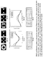
- Figs. 2a-2f in order to compare the impact of illumination on clear field and dark field imaging, three illumination modes were selected for comparison: (1) annular, (2) c-quad (cross-quad) and (3) dipole x, all with 0.93 NA immersion.
- the mask utilized to conduct the comparison was a binary intensity mask "BIM" with 70nm critical dimension (CD) at 175nm pitch.
- Figs. 2a and 2b show the diffraction pattern in the lens pupil for clear field (70nm chrome line, 105nm space) and dark field (70nm clear, 105nm chrome), respectively.
- the resulting first order diffraction pattern is the same, but the 0 th diffraction order amplitude is different for all three illuminations.
- FIG. 2c is the resulting aerial image intensity of the clear field mask for each of the illuminations
- Fig. 2d is the resulting aerial image intensity of the dark field mask for each of the illuminations
- Fig. 2e shows the corresponding NILS (normalized image log slope), minimum intensity (I min ) and the threshold value to print to 70nm line for each of the illuminations for the clear field mask
- Fig. 2f does the same for the dark field mask.
- the x-dipole illumination provides the best NILS and best I min in both the clear field and dark field cases.
- C-quad has the worst contrast and highest I min (in the clear field case, and lowest I min in the dark field case) which is due to the fact that only 25% of the first-order diffracted light is contributing to imaging while for the x-dipole, 50% of the 1 st order diffracted light is captured for imaging.
- the imaging threshold for all three illuminations is very close to 0.35 of intensity level, thus the dose required to print to the line CD target should be comparable.
- dipole gives the best image quality while c-quad is the worst of the three.
- Equation 3 the only difference between the clear field mask and the dark field mask is amplitude of the 0 th diffraction order.
- the 1 st diffractive order has the same amplitude with the opposite sign.
- the 0 th diffraction order amplitude for the clear field mask is 0.67
- the 0 th diffraction order amplitude is 0.33
- the magnitude of the diffraction order amplitude is the same for clear field and dark field mask with opposite signs.
- Fig. 4c and Fig. 4d illustrate the corresponding aerial images for clear field mask and dark field mask, respectively.
- Fig. 4e is the respective NILS, minimum or maximum intensity (I min /I max ), and the intensity threshold value to print to 70nm line (clear field) and space (dark field).
- I max minimum or maximum intensity
- the intensity threshold value to print to 70nm line (clear field) and space (dark field).
- the dark field mask has a higher mask error factor (MEF) which causes more difficulty for printing and applying OPC.
- MEF mask error factor
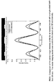
- Fig. 5 is an example illustrating the normalized energy captured by the lens pupil for a line and space for a feature (i.e., line or trench) having a CD of 70nm at 175nm pitch.
- Figs. 7b-7e illustrate simulated aerial images of a double dipole dark field imaging process in accordance with the present invention.
- Fig. 7a provides a simulated aerial image utilizing an annular illumination so as to provide a performance comparison with the dark field double dipole imaging process of the present invention.
- a trench having a width of 55nm and 210nm pitch is being imaged, and the intensity threshold level is set to be 34% in order to resolve the densest pitch.
- the conventional prior art approach for printing such small trenches is to apply a positive bias to the trench for better printability.
- the mask needs to be biased to 77nm; yet, the NILS value is only 0.82, which is too low to be manufacturable.
- the x-dipole i.e., labeled pass 1 in Fig. 7b
- the y-dipole exposing the horizontal mask (i.e., labeled as mask 2 bias in Fig. 7b) to resolve the trench in the horizontal direction.
- FIG. 7e illustrates the resulting aerial image of the combined (i.e., double dipole) imaging process.
- the resulting NILS is 1.83 at a threshold of 34%, which represents approximately 120% in NILS compared with the single, annular illumination process illustrated in Fig. 7a.
- the double exposure simulation result illustrated in Fig. 7b shows that the NILS (i.e., imaging performance) is not only a function of vertical trench size, but also as a function of the mask 2 bias. Indeed, variations in the mask 2 bias for the y-dipole exposure causes a significant change in the resulting overall NILS. As such, the combination of the bias from both masks can be used to optimize the overall NILS. This results from the fact that in the second exposure, it is possible to keep the vertical trench edge open to allow more light to pass through (see, Fig. 7d) to help optimize the NILS of the combined intensity.
- Figs 7c, 7d, and 7e illustrate an example of the optimization process.
- the vertical mask is biased to 65nm (see, Fig. 7c) and the vertical edge in the horizontal mask is negatively biased to 35nm.
- the NILS of the combined intensity is 1.83, which is about a 120% improvement in NILS, compared with the single exposure baseline.
- the bias associated with each mask can be adjusted in an effort to optimize the imaging performance.
- the NILS is utilized as the criteria defining imaging performance in the biasing optimization process, however, any other suitable criteria, such as, for example, DOF, MEF, ILS, NILS, contrast, etc., can be utilized.
- the optimization process it is also possible for the optimization process to be such that the bias of both masks are optimized simultaneously or in a serial manner.
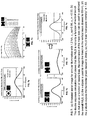
- Fig. 8 illustrates an exemplary flow chart of a process for decomposing a target pattern into vertical mask and a horizontal mask for use with dark field double dipole lithography in accordance with the present invention.
- Figs. 9a-9j illustrate an example of how the masks are generated utilizing the process of Fig. 8.
- the first step in the process (Step 90) is to obtain the desired target pattern to be imaged on a wafer or substrate.
- the target pattern may be represented in, for example, GDSII design data format, or any other suitable data format.
- Fig. 9a illustrates the exemplary target pattern utilized in the example.
- Steps 91, 93, 95 and 97 shown in Fig. 8 correspond to the generation of the horizontal mask or H-mask
- Steps 92, 94, 96 and 98 correspond to the generation of the vertical mask or V-mask.
- the bias for the low contrast feature of the given mask is optimized utilizing, for example, a suitable simulation model which operates to maximize a defined criteria, such as for example, but not limited to, DOF, MEF, NILS, ILS, contrast, etc.
- a suitable simulation model which operates to maximize a defined criteria, such as for example, but not limited to, DOF, MEF, NILS, ILS, contrast, etc.
- the bias of the vertical features i.e., low contrast features in the H-mask
- the bias of the horizontal features i.e., low contrast features in the V-mask
- Steps 93 and 94 the initial external scattering bars and internal scattering bars (which in the case of dark field masks are slots) are applied to the respective masks, and then the biasing of the low contrast feature of the respective mask is performed again so as to obtain the final biasing.
- Step 93 external and internal scattering bars are applied to the H-mask as required.
- the scattering bars can be applied utilizing any suitable rule based or model based method for applying scattering bars.
- the bias of the vertical features i.e., low contrast features in the H-mask
- Fig. 9d illustrates the H-mask after performing Step 93 in accordance with the given example.
- Step 94 external and internal scattering bars are applied to the V-mask as required, and then, with the scattering bars applied to the V-mask design, the bias of the horizontal features (i.e., low contrast features in the H-mask) are again optimized.
- Fig. 9e illustrates the V-mask after performing Step 94 in accordance with the given example.
- Step 95 the H-mask is subjected to a model OPC treatment (any suitable model OPC treatment may be utilized) and mask manufacturability verification.
- the resulting H-mask of the given example is illustrated in Fig. 9f.
- the H-mask is finalized (Step 97) and is ready to be utilized in the dark field double dipole imaging process.
- the H-mask is illuminated utilizing the y-dipole illumination shown in Fig. 9h.
- the V-mask is subjected to a model OPC treatment (any suitable model OPC treatment may be utilized) and mask manufacturability verification.
- the resulting V-mask of the given example is illustrated in Fig. 9g.
- the V-mask is finalized (Step 98) and is ready to be utilized in the dark field double dipole imaging process.
- the V-mask is illuminated utilizing the x-dipole illumination shown in Fig. 9i.
- Fig. 9j illustrates the resulting image of the double dipole process utilizing the dark field H-mask and V-mask process.
- Fig. 10 illustrates an actual example of the layout conversion method of the present invention and the resulting image.
- a 70nm trench at 140nm pitch comb target test pattern was decomposed into a H-mask and V-mask in accordance with the foregoing process, and the H-mask and V-mask were illuminated with the y-dipole and x-dipole illumination, respectively.
- the resulting image accurately reproduces the target pattern.
- the method of the present invention provides important advantages over the prior art. Most importantly, by utilizing a dark field mask in the double dipole imaging process, it is possible to eliminate the issues associated with shielding previously imaged features when utilizing a clear field imaging process.
- Fig. 11 illustrates an exemplary processing system for performing the decomposition process of the present invention.
- an exemplary processing system may contain a processor 1000 which receives input from an input 1003.
- Processor 1000 may be a conventional microprocessor or may be a specially designed processing unit, such as an EEPROM or EPROM or a fabricated integrated circuit.
- Input 1003 may be any type of electronic input device, such as a keyboard or a mouse, or may be a memory or internet connection.
- Processor 1000 preferably retrieves stored protocols from ROM 1002 and RAM 1001, such as protocols to implement the methods detailed above for decomposing customized DOEs in accordance with the present invention, and stores information on RAM 1001.
- the calculated results (e.g., DOE design) of processor 1000 may be displayed on display 1004 and may be provided to a mask fabrication device or manufacturer.
- the software functionalities of such a computer system involve programming, including executable code, may be used to implement the above described OPC method for placing scattering bars within a given target pattern.
- the software code is executable by the general-purpose computer.
- the code and possibly the associated data records are stored within a general-purpose computer platform.
- the software may be stored at other locations and/or transported for loading into the appropriate general-purpose computer systems.
- the embodiments discussed above involve one or more software products in the form of one or more modules of code carried by at least one machine-readable medium. Execution of such code by a processor of the computer system enables the platform to implement the catalog and/or software downloading functions, in essentially the manner performed in the embodiments discussed and illustrated herein.
- Non-volatile media include, for example, optical or magnetic disks, such as any of the storage devices in any computer(s) operating as one of the server platform, discussed above.
- Volatile media include dynamic memory, such as main memory of such a computer platform.
- Physical transmission media include coaxial cables; copper wire and fiber optics, including the wires that comprise a bus within a computer system.
- Carrier-wave transmission media can take the form of electric or electromagnetic signals, or acoustic or light waves such as those generated during radio frequency (RF) and infrared (IR) data communications.
- Common forms of computer-readable media therefore include, for example: a floppy disk, a flexible disk, hard disk, magnetic tape, any other magnetic medium, a CD-ROM, DVD, any other optical medium, less commonly used media such as punch cards, paper tape, any other physical medium with patterns of holes, a RAM, a PROM, and EPROM, a FLASH-EPROM, any other memory chip or cartridge, a carrier wave transporting data or instructions, cables or links transporting such a carrier wave, or any other medium from which a computer can read programming code and/or data.
- Many of these forms of computer readable media may be involved in carrying one or more sequences of one or more instructions to a processor for execution.
- Fig. 12 schematically depicts a lithographic projection apparatus suitable for use with the DOEs designed with the aid of the current invention.
- the apparatus comprises:
- the apparatus is of a transmissive type (i.e . has a transmissive mask). However, in general, it may also be of a reflective type, for example (with a reflective mask). Alternatively, the apparatus may employ another kind of patterning means as an alternative to the use of a mask; examples include a programmable mirror array or LCD matrix.
- the source LA (e.g . a mercury lamp, excimer laser or plasma discharge source) produces a beam of radiation.
- This beam is fed into an illumination system (illuminator) IL, either directly or after having traversed conditioning means, such as a beam expander Ex, for example.
- the illuminator IL may comprise adjusting means AM for setting the outer and/or inner radial extent (commonly referred to as ⁇ -outer and ⁇ -inner, respectively) of the intensity distribution in the beam.
- it will generally comprise various other components, such as an integrator IN and a condenser CO.
- the beam PB impinging on the mask MA has a desired uniformity and intensity distribution in its cross-section.
- the source LA and DOE may be within the housing of the lithographic projection apparatus (as is often the case when the source LA is a mercury lamp, for example), but that it may also be remote from the lithographic projection apparatus, the radiation beam that it produces being led into the apparatus (e.g. with the aid of suitable directing mirrors); this latter scenario is often the case when the source LA is an excimer laser (e.g. based on KrF, ArF or F 2 lasing).
- the current invention encompasses both of these scenarios.
- the beam PB subsequently intercepts the mask MA, which is held on a mask table MT. Having traversed the mask MA, the beam PB passes through the lens PL, which focuses the beam PB onto a target portion C of the substrate W. With the aid of the second positioning means (and interferometric measuring means IF), the substrate table WT can be moved accurately, e.g . so as to position different target portions C in the path of the beam PB. Similarly, the first positioning means can be used to accurately position the mask MA with respect to the path of the beam PB, e.g . after mechanical retrieval of the mask MA from a mask library, or during a scan.
- the mask table MT may just be connected to a short stroke actuator, or may be fixed.
- the depicted tool can be used in two different modes:
- the concepts disclosed herein may simulate or mathematically model any generic imaging system for imaging sub wavelength features, and may be especially useful with emerging imaging technologies capable of producing wavelengths of an increasingly smaller size.
- Emerging technologies already in use include EUV (extreme ultra violet) lithography that is capable of producing a 193nm wavelength with the use of a ArF laser, and even a 157nm wavelength with the use of a Fluorine laser.
- EUV lithography is capable of producing wavelengths within a range of 20-5nm by using a synchrotron or by hitting a material (either solid or a plasma) with high energy electrons in order to produce photons within this range.
- illumination may be produced by reflective mirrors with a multi-stack of Molybdenum and Silicon.
- the multi-stack mirror has a 40 layer pairs of Molybdenum and Silicon where the thickness of each layer is a quarter wavelength. Even smaller wavelengths may be produced with X-ray lithography.
- a synchrotron is used to produce an X-ray wavelength. Since most material is absorptive at x-ray wavelengths, a thin piece of absorbing material defines where features would print (positive resist) or not print (negative resist).
Abstract
Description
- The present invention provides a novel process for forming masks for use in double dipole lithography, and more specifically, a method for forming masks for use in dark field double dipole lithography process. In addition, the present invention relates to a device manufacturing method using a lithographic apparatus comprising a radiation system for providing a projection beam of radiation; a mask table for holding a reticle, serving to pattern the projection beam; a substrate table for holding a substrate; and a projection system for projecting the patterned projection beam onto a target portion of the substrate.
- Lithographic projection apparatus (tools) can be used, for example, in the manufacture of integrated circuits (ICs). In such a case, the mask contains a circuit pattern corresponding to an individual layer of the IC, and this pattern can be imaged onto a target portion (e.g. comprising one or more dies) on a substrate (silicon wafer) that has been coated with a layer of radiation-sensitive material (resist). In general, a single wafer will contain a whole network of adjacent target portions that are successively irradiated via the projection system, one at a time. In one type of lithographic projection apparatus, each target portion is irradiated by exposing the entire mask pattern onto the target portion in one go; such an apparatus is commonly referred to as a wafer stepper. In an alternative apparatus -commonly referred to as a step-and-scan apparatus - each target portion is irradiated by progressively scanning the mask pattern under the projection beam in a given reference direction (the "scanning" direction) while synchronously scanning the substrate table parallel or anti-parallel to this direction; since, in general, the projection system will have a magnification factor M (generally < 1), the speed V at which the substrate table is scanned will be a factor M times that at which the mask table is scanned. More information with regard to lithographic apparatus as here described can be gleaned, for example, from
US 6,046,792 , incorporated herein by reference. - In a manufacturing process using a lithographic projection apparatus, a mask pattern is imaged onto a substrate that is at least partially covered by a layer of radiation-sensitive material (resist). Prior to this imaging step, the substrate may undergo various procedures, such as priming, resist coating and a soft bake. After exposure, the substrate may be subjected to other procedures, such as a post-exposure bake (PEB), development, a hard bake and measurement/inspection of the imaged features. This array of procedures is used as a basis to pattern an individual layer of a device, e.g. an IC. Such a patterned layer may then undergo various processes such as etching, ion-implantation (doping), metallization, oxidation, chemo-mechanical polishing, etc., all intended to finish off an individual layer. If several layers are required, then the whole procedure, or a variant thereof, will have to be repeated for each new layer. Eventually, an array of devices will be present on the substrate (wafer). These devices are then separated from one another by a technique such as dicing or sawing. Thereafter, the individual devices can be mounted on a carrier, connected to pins, etc. Further information regarding such processes can be obtained, for example, from the book "Microchip Fabrication: A Practical Guide to Semiconductor Processing", Third Edition, by Peter van Zant, McGraw Hill Publishing Co., 1997, ISBN 0-07-067250-4, incorporated herein by reference.
- The lithographic tool may be of a type having two or more substrate tables (and/or two or more mask tables). In such "multiple stage" devices the additional tables may be used in parallel, or preparatory steps may be carried out on one or more tables while one or more other tables are being used for exposures. Twin stage lithographic tools are described, for example, in
US 5,969,441 andWO 98/40791 - The photolithography masks referred to above comprise geometric patterns corresponding to the circuit components to be integrated onto a silicon wafer. The patterns used to create such masks are generated utilizing CAD (computer-aided design) programs, this process often being referred to as EDA (electronic design automation). Most CAD programs follow a set of predetermined design rules in order to create functional masks. These rules are set by processing and design limitations. For example, design rules define the space tolerance between circuit devices (such as gates, capacitors, etc.) or interconnect lines, so as to ensure that the circuit devices or lines do not interact with one another in an undesirable way.
- Of course, one of the goals in integrated circuit fabrication is to faithfully reproduce the original circuit design on the wafer (via the mask). Another goal is to use as much of the semiconductor wafer real estate as possible. As the size of an integrated circuit is reduced and its density increases, however, the CD (critical dimension) of its corresponding mask pattern approaches the resolution limit of the optical exposure tool. The resolution for an exposure tool is defined as the minimum feature that the exposure tool can repeatedly expose on the wafer. The resolution value of present exposure equipment often constrains the CD for many advanced IC circuit designs.
- Furthermore, as the demand continues for even higher performance of semiconductor devices, the design rule shrink rate is outpacing the progress of both of the exposure wavelength reduction and the advancement of high Numerical Aperture (NA) lenses. This factor has presented a challenge to lithographers to push optical lithography beyond the limit that was thought possible a few years ago. As is known, Resolution Enhancement Techniques (RETs) have become indispensable in low k1 optical lithography. Strong Off-Axis Illumination (OAI), which uses 2-beam imaging with symmetrical 0th and 1st orders in the lens pupil, can greatly enhance resolution and contrast. Dipole illumination is the most extreme case of OAI, and is capable of providing better imaging contrast with improved process latitude for very low k1 imaging.
- Current techniques utilizing dipole illumination typically encompass the use of a multiple exposure process in which a first exposure is utilized to image features oriented in a first direction (i.e., horizontally oriented features) and a second exposure is utilized to image features oriented in a second direction (i.e., vertically oriented features). This is accomplished by converting the target pattern into, for example, two masks having horizontal and vertical orientations, respectively. Once the target pattern is converted in this manner, a y-dipole exposure is utilized to image the horizontally oriented features, and a x-dipole exposure is utilized to image the vertically oriented features.
- As known dipole imaging techniques utilize a clear field mask, one important aspect of double dipole illumination is that when imaging the horizontally oriented features, the vertically oriented features must be protected (i.e., shielded) so the vertically oriented features are not degraded. The opposite is true when vertically oriented features are imaged (i.e., the horizontally oriented features must be protected). This shielding requirement can lead to mask making complications as well as limit the overall performance of the imaging process.
- Accordingly, there exists a need for a method which allows for performing double dipole lithography utilizing a dark field mask so as to eliminate the complications that result from the shielding requirements necessary when utilizing clear field masks in a double dipole lithography process.
- In an effort to solve the foregoing needs, it is one object of the present invention to provide a method for performing dark field double dipole lithography. As noted above, by utilizing a dark field in the imaging process, it is possible to eliminate the issues associated with shielding previously imaged features when utilizing a clear field imaging process.
- More specifically, the present invention relates to a method of generating complementary masks for use in a dark field double dipole imaging process. The method includes the steps of identifying a target pattern having a plurality of features, including horizontal and vertical features; generating a horizontal mask based on the target pattern, where the horizontal mask includes low contrast vertical features. The generation of the horizontal mask includes the steps of optimizing the bias of the low contrast vertical features contained in the horizontal mask; and applying scatter bars to the horizontal mask. The method further includes generating a vertical mask based on the target pattern, where the vertical mask contains low contrast horizontal features. The generation of the vertical mask includes the steps of optimizing the bias of low contrast horizontal features contained in the vertical mask; and applying scatter bars to the vertical mask.
- The present invention also relates to a computer readable medium configured to store program instructions for execution by a processor. The program instructions enable the processor to generate files corresponding to complementary masks for use in a dark field double dipole imaging process. The generation of the files includes the steps of identifying a target pattern having a plurality of features, including horizontal and vertical features; generating a horizontal mask based on the target pattern, where the horizontal mask includes low contrast vertical features. The generation of the horizontal mask includes the steps of optimizing the bias of the low contrast vertical features contained in the horizontal mask; and applying scatter bars to the horizontal mask. The generation of the files further includes generating a vertical mask based on the target pattern, where the vertical mask contains low contrast horizontal features. The generation of the vertical mask includes the steps of optimizing the bias of low contrast horizontal features contained in the vertical mask; and applying scatter bars to the vertical mask.
- Although specific reference may be made in this text to the use of the invention in the manufacture ofICs, it should be explicitly understood that the invention has many other possible applications. For example, it may be employed in the manufacture of integrated optical systems, guidance and detection patterns for magnetic domain memories, liquid-crystal display panels, thin-film magnetic heads, etc. The skilled artisan will appreciate that, in the context of such alternative applications, any use of the terms "reticle", "wafer" or "die" in this text should be considered as being replaced by the more general terms "mask", "substrate" and "target portion", respectively.
- In the present document, the terms "radiation" and "beam" are used to encompass all types of electromagnetic radiation, including ultraviolet radiation (e.g. with a wavelength of 365, 248, 193, 157 or 126 nm) and EUV (extreme ultra-violet radiation, e.g. having a wavelength in the range 5-20 nm).
- The term mask as employed in this text may be broadly interpreted as referring to generic patterning means that can be used to endow an incoming radiation beam with a patterned cross-section, corresponding to a pattern that is to be created in a target portion of the substrate; the term "light valve" can also be used in this context. Besides the classic mask (transmissive or reflective; binary, phase-shifting, hybrid, etc.), examples of other such patterning means include:
- a) A programmable mirror array. An example of such a device is a matrix-addressable surface having a viscoelastic control layer and a reflective surface. The basic principle behind such an apparatus is that (for example) addressed areas of the reflective surface reflect incident light as diffracted light, whereas unaddressed areas reflect incident light as undiffracted light. Using an appropriate filter, the said undiffracted light can be filtered out of the reflected beam, leaving only the diffracted light behind; in this manner, the beam becomes patterned according to the addressing pattern of the matrix-addressable surface. The required matrix addressing can be performed using suitable electronic means. More information on such mirror arrays can be gleaned, for example, from
United States Patents US 5,296,891 andUS 5,523,193 , which are incorporated herein by reference. - b) A programmable LCD array. An example of such a construction is given in
United States Patent US 5,229,872 , which is incorporated herein by reference. - The method of the present invention provides important advantages over the prior art. Most importantly, by utilizing a dark field mask in the double dipole imaging process, it is possible to eliminate the issues associated with shielding previously imaged features when utilizing a clear field imaging process.
- Additional advantages of the present invention will become apparent to those skilled in the art from the following detailed description of exemplary embodiments of the present invention.
- The invention itself, together with further objects and advantages, can be better understood by reference to the following detailed description and the accompanying schematic drawings, in which
- Fig. 1 a illustrates normalized design rule requirements for the various components found in a typically IC design.
- Fig. 1b illustrates the resulting NILS for various illumination conditions for a 45nm half pitch where mask CD varies from 45nm to 100nm under different k1 conditions.
- Figs. 2a-2f compare the impact of illumination on clear field and dark field imaging.
- Fig. 3 illustrates an exemplary 1-dimensional mask grating.
- Figs. 4a and 4b illustrate exemplary the diffraction patterns associated with a 70nm line (i.e., clear field) and a 70nm space (dark field).
- Figs. 4c and Fig. 4d illustrate the corresponding aerial images for clear field mask and dark field mask associated with the 70nm line (i.e., clear field) and the 70nm space (dark field) of Fig. 4a and 4b, respectively.
- Fig. 4e is the respective NILS, minimum or maximum intensity (Imin/Imax), and the intensity threshold value to print to 70nm line (clear field) and space (dark field) associated with Fig. 4a and 4b, respectively.
- Fig. 5 is an example illustrating the normalized energy captured by the lens pupil for a line and space for a feature (i.e., line or trench) having a CD of 70nm at 175nm pitch.
- Fig. 6 illustrates a comparison of the resulting aerial image of an isolated trench with a single sided dark field SB slot for rigorous EMF versus a scalar model.
- Fig. 7a illustrates a simulated aerial image of a trench utilizing an annular illumination.
- Figs. 7b-7e illustrate simulated aerial images of a double dipole dark field imaging process in accordance with the present invention.
- Fig. 8 illustrates an exemplary flow chart of a process for decomposing a target pattern into vertical mask and a horizontal mask for use with dark field double dipole lithography in accordance with the present invention.
- Figs. 9a-9j illustrate an example of how the masks are generated utilizing the process of Fig. 8.
- Fig. 10 illustrates an actual example of the layout conversion method of the present invention and the resulting image.
- Fig. 11 illustrates an exemplary processing system for implementing the decomposition method of the present invention.
- Fig. 12 schematically depicts a lithographic projection apparatus suitable for use with the masks designed with the aid of the current invention.
- As explained in more detail below, the preferred embodiment of the present invention provides a method and apparatus for performing dark field double dipole lithography "DDL". Specifically, the present invention provides a method for decomposing a target pattern into a first mask to be imaged utilizing a first dipole illumination (i.e., x-dipole) and a second mask to be imaged utilizing a second dipole illumination (i.e., y-dipole), where the mask utilize dark field imaging. Prior to discussing the present invention, a brief discussion of clear field and dark field imaging is provided.
- Clear field DDL, which can be utilized with immersion and polarization, is a good resolution enhancement technique "RET" solution for various imaging tasks, such as imaging a poly-gate layer. Advantages associated with the clear field DDL techniques are, for example, that it resolves the scalability and printability problem for scattering bars (SB) or assist features (AF); allows printing devices using high contrast dipole illumination; and enables application of linear polarization for patterning device structures based on model based layout conversion methods.
- Referring to Fig. 1a, the
metal 1 pitch of an IC design is often utilized as one of the fundamental measures for successive device generations because themetal 1 pitch of a given design typically defines the density of integration and is therefore the dimension that is driven the hardest from a pitch shrinking perspective. Presently, the back end metal interconnects processing typically utilizes a low-k dielectric with copper damascene integration scheme that requires printing small dimension trenches at very tight pitches. Due to the inherent high contrast associated with dipole illumination, it is a good illumination choice for imaging such dense trenches. Fig. 1b shows the simulated normalized image log slope (NILS=CD*ILS) "NILS" for 45nm half pitch where mask CD varies from 45 to 100 nm versus different k1, where k1 = 0.5 pitch * NA/λ, where NA corresponds to the numerical aperture and λ corresponds to the exposure wavelength of the illumination device. The general trend of Fig. 1b shows that the lower the k1, the worse the resulting NILS. For the 45nm node, features CD on wafer are closer to a quarter of the exposure wavelength, which makes dark field imaging challenging. As such, dipole illumination is a good candidate to improve the NILS (higher NILS corresponds to higher contrast and therefore better imaging). It is noted that in Fig. 1b, for the 45nm node even with the most aggressive "hard" dipole setting with very small sigma delta between sigma in and sigma out, the NILS is still too low to achieve a robust imaging. Only when dipole imaging is combined with linear polarization is there sufficient contrast for imaging at k1 near 0.3. - Referring to Figs. 2a-2f, in order to compare the impact of illumination on clear field and dark field imaging, three illumination modes were selected for comparison: (1) annular, (2) c-quad (cross-quad) and (3) dipole x, all with 0.93 NA immersion. The mask utilized to conduct the comparison was a binary intensity mask "BIM" with 70nm critical dimension (CD) at 175nm pitch. Figs. 2a and 2b show the diffraction pattern in the lens pupil for clear field (70nm chrome line, 105nm space) and dark field (70nm clear, 105nm chrome), respectively. The resulting first order diffraction pattern is the same, but the 0th diffraction order amplitude is different for all three illuminations. Fig. 2c is the resulting aerial image intensity of the clear field mask for each of the illuminations, and Fig. 2d is the resulting aerial image intensity of the dark field mask for each of the illuminations. Fig. 2e shows the corresponding NILS (normalized image log slope), minimum intensity (Imin) and the threshold value to print to 70nm line for each of the illuminations for the clear field mask, while Fig. 2f does the same for the dark field mask.
- As is shown, the x-dipole illumination provides the best NILS and best Imin in both the clear field and dark field cases. C-quad has the worst contrast and highest Imin (in the clear field case, and lowest Imin in the dark field case) which is due to the fact that only 25% of the first-order diffracted light is contributing to imaging while for the x-dipole, 50% of the 1st order diffracted light is captured for imaging. It is noted that for the clear field case, the imaging threshold for all three illuminations is very close to 0.35 of intensity level, thus the dose required to print to the line CD target should be comparable. For both clear field and dark field cases, dipole gives the best image quality while c-quad is the worst of the three.
- In order to understand the fundamental difference between clear field and dark field imaging under dipole illumination, it is first necessary to understand the difference in the respective diffraction patterns. Consider a point on the source and a 1-D grating (see, Fig. 3) of width (w), pitch (p) and intensity transmission (T). This mask can be expressed as:


0th order,
± 1 orders,


- From
Equation 1, it is clear that for a dark field mask with a fixed trench CD, the larger the pitch, the smaller the 0th diffraction order. Babinet's principle states that the diffraction pattern of two complementary masks have the same diffraction pattern except the 0th order. Babinet's principle can be written as:
- From
Equation 3, the only difference between the clear field mask and the dark field mask is amplitude of the 0th diffraction order. The 1st diffractive order has the same amplitude with the opposite sign.

- From Equation 4, it is evident that for a clear field mask, the larger the pitch, the lower the 0th diffraction order. The above discussions only consider one point from the source, but it is useful to understand the example in Figs. 4a and 4b which illustrates the diffraction patterns for a 70nm line (i.e., clear field) and a 70nm space (dark field) at 1:1, 1:1.5, and 1:2 ratios, respectively. For 1:1 ratio (i.e., feature width-to-pitch), both clear and dark field cases are the same. From 1:1.5 to 1:2 ratios upward, there is a significant difference in the 0th diffraction order amplitude. For example, with the 1:2 ratio; the 0th diffraction order amplitude for the clear field mask is 0.67, while for the dark field mask the 0th diffraction order amplitude is 0.33. For the first and second diffraction orders, the magnitude of the diffraction order amplitude is the same for clear field and dark field mask with opposite signs.
- Fig. 4c and Fig. 4d illustrate the corresponding aerial images for clear field mask and dark field mask, respectively. In the given example, the illumination settings assume the use of an ASML scanner with 0.93NA and dipole x, 35 degree pole angle, the σ_out = 0.86 and σ_in=0.45. Fig. 4e is the respective NILS, minimum or maximum intensity (Imin/Imax), and the intensity threshold value to print to 70nm line (clear field) and space (dark field). As can be seen, not only does Imax change more drastically for the dark field mask, but the NILS is also 20-30% lower than the clear field complementary mask. Therefore, the dark field mask has a higher mask error factor (MEF) which causes more difficulty for printing and applying OPC.
- For dark field imaging, it is important to have sufficient energy to clear up the resist for patterning trenches which are mainly contributed by 0th diffraction order, even though the 0th diffraction order does not contribute to intensity modulation. For partial coherent imaging, the overlaps of each of the diffraction orders within the NA need to be considered and the energy captured by the lens pupil per diffraction order needs to be computed. Fig. 5 is an example illustrating the normalized energy captured by the lens pupil for a line and space for a feature (i.e., line or trench) having a CD of 70nm at 175nm pitch. Comparing the normalized energy captured by the pupil, it is clear that the energy that comes from the +/first order for line and trench are identical, but there is a 2X difference in 0th diffraction order energy. This is one of the reasons that the trench layers typically have a positive mask bias to allow more light/energy to pass through.
- When utilizing clear field DDL, it is typically necessary to use "full-sized" scattering bars (FSB) in order to achieve a robust through-pitch process window. Further, as noted above, the larger the pitch, the higher the 0th diffraction order, so it is necessary to add shielding for the critical features in the respective low contrast orientation. Further, in clear field DDL, the sum of the total exposure can trim away the FSB without leaving the print residues. This cannot be done in dark field DDL. However, in order to improve the depth of focus for a manufacturing-worthy process, "dark-field SB" slots, or sub-resolution assist slots can be added during the optical proximity correction "OPC" process.
- It can be problematic to apply the dark field SB slot for 45nm node and beyond. Specifically, as the width of a dark field SB slot on the 4X reticle becomes less than the exposure wavelength, Kirchhoff scalar diffraction theory starts to break down and it over predicts SB slot intensity level. Referring to Fig. 6, which compares the resulting aerial image of an isolated trench with a single sided dark field SB slot for rigorous EMF (i.e., the model considers the full electromagnetic field when determining the aerial image) versus scalar model (i.e., a more ideal model, which does not include effects of the full electromagnetic field), the EMF aerial image indicates that the dark-field SB slot is actually "smaller" than the scalar theory has predicted. This implies that the SB slots have less optical weight than the scalar theory predicted. Therefore, a larger sub-resolution dark-field SB slot is less likely to print. The risk of printing a dark field SB slot increases when the spacing between the main features is smaller. This limits when to start applying the SB effectively. Fortunately, both rigorous EMF models and scalar models predict the same position to apply dark-field SB slot. Therefore, it is possible to optimize the placement of the dark-field SB slot utilizing the less rigorous and time consuming scalar model. To achieve more accurate model OPC results, a quasi-rigorous approach such as a boundary layer method is required.
- Figs. 7b-7e illustrate simulated aerial images of a double dipole dark field imaging process in accordance with the present invention. Fig. 7a provides a simulated aerial image utilizing an annular illumination so as to provide a performance comparison with the dark field double dipole imaging process of the present invention. In the given example, a trench having a width of 55nm and 210nm pitch is being imaged, and the intensity threshold level is set to be 34% in order to resolve the densest pitch. The conventional prior art approach for printing such small trenches is to apply a positive bias to the trench for better printability. As noted, Fig. 7a provides the simulation result for annular illumination with 1.2 NA, σ_out=0.98, σ_in =0.53. In order to print the trench to the desired CD, the mask needs to be biased to 77nm; yet, the NILS value is only 0.82, which is too low to be manufacturable.
- For a double exposure process, relative intensity level from two exposures cannot be directly summed. However, the dose and photo-acid that is generated from the two exposures are cumulative. For chemical amplified resist, the photo-acid concentration is given by Eq. 6.

pass 1 in Fig. 7b) is used to image the trench in the vertical mask), followed by the y-dipole exposing the horizontal mask (i.e., labeled asmask 2 bias in Fig. 7b) to resolve the trench in the horizontal direction. Fig. 7e illustrates the resulting aerial image of the combined (i.e., double dipole) imaging process. As shown, the resulting NILS is 1.83 at a threshold of 34%, which represents approximately 120% in NILS compared with the single, annular illumination process illustrated in Fig. 7a. - Importantly, the double exposure simulation result illustrated in Fig. 7b shows that the NILS (i.e., imaging performance) is not only a function of vertical trench size, but also as a function of the
mask 2 bias. Indeed, variations in themask 2 bias for the y-dipole exposure causes a significant change in the resulting overall NILS. As such, the combination of the bias from both masks can be used to optimize the overall NILS. This results from the fact that in the second exposure, it is possible to keep the vertical trench edge open to allow more light to pass through (see, Fig. 7d) to help optimize the NILS of the combined intensity. Figs 7c, 7d, and 7e illustrate an example of the optimization process. In the above example, the vertical mask is biased to 65nm (see, Fig. 7c) and the vertical edge in the horizontal mask is negatively biased to 35nm. As noted, the NILS of the combined intensity is 1.83, which is about a 120% improvement in NILS, compared with the single exposure baseline. Thus, in accordance with the present invention the bias associated with each mask can be adjusted in an effort to optimize the imaging performance. It is noted that in the given example, the NILS is utilized as the criteria defining imaging performance in the biasing optimization process, however, any other suitable criteria, such as, for example, DOF, MEF, ILS, NILS, contrast, etc., can be utilized. Moreover, it is also possible for the optimization process to be such that the bias of both masks are optimized simultaneously or in a serial manner. - Fig. 8 illustrates an exemplary flow chart of a process for decomposing a target pattern into vertical mask and a horizontal mask for use with dark field double dipole lithography in accordance with the present invention. Figs. 9a-9j illustrate an example of how the masks are generated utilizing the process of Fig. 8. Referring to Fig. 8, the first step in the process (Step 90) is to obtain the desired target pattern to be imaged on a wafer or substrate. The target pattern may be represented in, for example, GDSII design data format, or any other suitable data format. Fig. 9a illustrates the exemplary target pattern utilized in the example. Once the target pattern is defined, it is decomposed into vertical and horizontal masks, where
Steps Steps - More specifically, in
Steps Step 91, as shown in Fig, 9b, the bias of the vertical features (i.e., low contrast features in the H-mask) are optimized in the H-mask. Similarly, inStep 92, as shown in Fig. 9c, the bias of the horizontal features (i.e., low contrast features in the V-mask) are optimized in the V-mask. Next, inSteps Step 93, external and internal scattering bars are applied to the H-mask as required. The scattering bars can be applied utilizing any suitable rule based or model based method for applying scattering bars. Then, with the scattering bars applied to the H-mask design, the bias of the vertical features (i.e., low contrast features in the H-mask) are again optimized. Fig. 9d illustrates the H-mask after performingStep 93 in accordance with the given example. Similarly, inStep 94, external and internal scattering bars are applied to the V-mask as required, and then, with the scattering bars applied to the V-mask design, the bias of the horizontal features (i.e., low contrast features in the H-mask) are again optimized. Fig. 9e illustrates the V-mask after performingStep 94 in accordance with the given example. Next, inStep 95, the H-mask is subjected to a model OPC treatment (any suitable model OPC treatment may be utilized) and mask manufacturability verification. The resulting H-mask of the given example is illustrated in Fig. 9f. After completion ofStep 95, the H-mask is finalized (Step 97) and is ready to be utilized in the dark field double dipole imaging process. The H-mask is illuminated utilizing the y-dipole illumination shown in Fig. 9h. Similarly, inStep 96, the V-mask is subjected to a model OPC treatment (any suitable model OPC treatment may be utilized) and mask manufacturability verification. The resulting V-mask of the given example is illustrated in Fig. 9g. After completion ofStep 96, the V-mask is finalized (Step 98) and is ready to be utilized in the dark field double dipole imaging process. The V-mask is illuminated utilizing the x-dipole illumination shown in Fig. 9i. Fig. 9j illustrates the resulting image of the double dipole process utilizing the dark field H-mask and V-mask process. - Fig. 10 illustrates an actual example of the layout conversion method of the present invention and the resulting image. Specifically, a 70nm trench at 140nm pitch comb target test pattern was decomposed into a H-mask and V-mask in accordance with the foregoing process, and the H-mask and V-mask were illuminated with the y-dipole and x-dipole illumination, respectively. As shown, the resulting image accurately reproduces the target pattern.
- The method of the present invention provides important advantages over the prior art. Most importantly, by utilizing a dark field mask in the double dipole imaging process, it is possible to eliminate the issues associated with shielding previously imaged features when utilizing a clear field imaging process.
- Fig. 11 illustrates an exemplary processing system for performing the decomposition process of the present invention. As illustrated in Fig. 11, an exemplary processing system may contain a
processor 1000 which receives input from aninput 1003.Processor 1000 may be a conventional microprocessor or may be a specially designed processing unit, such as an EEPROM or EPROM or a fabricated integrated circuit.Input 1003 may be any type of electronic input device, such as a keyboard or a mouse, or may be a memory or internet connection.Processor 1000 preferably retrieves stored protocols fromROM 1002 andRAM 1001, such as protocols to implement the methods detailed above for decomposing customized DOEs in accordance with the present invention, and stores information onRAM 1001. The calculated results (e.g., DOE design) ofprocessor 1000 may be displayed ondisplay 1004 and may be provided to a mask fabrication device or manufacturer. - The software functionalities of such a computer system involve programming, including executable code, may be used to implement the above described OPC method for placing scattering bars within a given target pattern. The software code is executable by the general-purpose computer. In operation, the code and possibly the associated data records are stored within a general-purpose computer platform. At other times, however, the software may be stored at other locations and/or transported for loading into the appropriate general-purpose computer systems. Hence, the embodiments discussed above involve one or more software products in the form of one or more modules of code carried by at least one machine-readable medium. Execution of such code by a processor of the computer system enables the platform to implement the catalog and/or software downloading functions, in essentially the manner performed in the embodiments discussed and illustrated herein.
- As used herein, terms such as computer or machine "readable medium" refer to any medium that participates in providing instructions to a processor for execution. Such a medium may take many forms, including but not limited to, non-volatile media, volatile media, and transmission media. Non-volatile media include, for example, optical or magnetic disks, such as any of the storage devices in any computer(s) operating as one of the server platform, discussed above. Volatile media include dynamic memory, such as main memory of such a computer platform. Physical transmission media include coaxial cables; copper wire and fiber optics, including the wires that comprise a bus within a computer system. Carrier-wave transmission media can take the form of electric or electromagnetic signals, or acoustic or light waves such as those generated during radio frequency (RF) and infrared (IR) data communications. Common forms of computer-readable media therefore include, for example: a floppy disk, a flexible disk, hard disk, magnetic tape, any other magnetic medium, a CD-ROM, DVD, any other optical medium, less commonly used media such as punch cards, paper tape, any other physical medium with patterns of holes, a RAM, a PROM, and EPROM, a FLASH-EPROM, any other memory chip or cartridge, a carrier wave transporting data or instructions, cables or links transporting such a carrier wave, or any other medium from which a computer can read programming code and/or data. Many of these forms of computer readable media may be involved in carrying one or more sequences of one or more instructions to a processor for execution.
- Fig. 12 schematically depicts a lithographic projection apparatus suitable for use with the DOEs designed with the aid of the current invention. The apparatus comprises:
- a radiation system Ex, IL, for supplying a projection beam PB of radiation. In this particular case, the radiation system also comprises a radiation source LA;
- a first object table (mask table) MT provided with a mask holder for holding a mask MA (e.g. a reticle), and connected to first positioning means for accurately positioning the mask with respect to item PL;
- a second object table (substrate table) WT provided with a substrate holder for holding a substrate W (e.g. a resist-coated silicon wafer), and connected to second positioning means for accurately positioning the substrate with respect to item PL;
- a projection system ("lens") PL (e.g. a refractive, catoptric or catadioptric optical system) for imaging an irradiated portion of the mask MA onto a target portion C (e.g. comprising one or more dies) of the substrate W.
- As depicted herein, the apparatus is of a transmissive type (i.e. has a transmissive mask). However, in general, it may also be of a reflective type, for example (with a reflective mask). Alternatively, the apparatus may employ another kind of patterning means as an alternative to the use of a mask; examples include a programmable mirror array or LCD matrix.
- The source LA (e.g. a mercury lamp, excimer laser or plasma discharge source) produces a beam of radiation. This beam is fed into an illumination system (illuminator) IL, either directly or after having traversed conditioning means, such as a beam expander Ex, for example. The illuminator IL may comprise adjusting means AM for setting the outer and/or inner radial extent (commonly referred to as σ-outer and σ-inner, respectively) of the intensity distribution in the beam. In addition, it will generally comprise various other components, such as an integrator IN and a condenser CO. In this way, the beam PB impinging on the mask MA has a desired uniformity and intensity distribution in its cross-section.
- It should be noted with regard to Fig. 12 that the source LA and DOE may be within the housing of the lithographic projection apparatus (as is often the case when the source LA is a mercury lamp, for example), but that it may also be remote from the lithographic projection apparatus, the radiation beam that it produces being led into the apparatus (e.g. with the aid of suitable directing mirrors); this latter scenario is often the case when the source LA is an excimer laser (e.g. based on KrF, ArF or F2 lasing). The current invention encompasses both of these scenarios.
- The beam PB subsequently intercepts the mask MA, which is held on a mask table MT. Having traversed the mask MA, the beam PB passes through the lens PL, which focuses the beam PB onto a target portion C of the substrate W. With the aid of the second positioning means (and interferometric measuring means IF), the substrate table WT can be moved accurately, e.g. so as to position different target portions C in the path of the beam PB. Similarly, the first positioning means can be used to accurately position the mask MA with respect to the path of the beam PB, e.g. after mechanical retrieval of the mask MA from a mask library, or during a scan. In general, movement of the object tables MT, WT will be realized with the aid of a long-stroke module (coarse positioning) and a short-stroke module (fine positioning), which are not explicitly depicted in Fig. 12. However, in the case of a wafer stepper (as opposed to a step-and-scan tool) the mask table MT may just be connected to a short stroke actuator, or may be fixed.
- The depicted tool can be used in two different modes:
- In step mode, the mask table MT is kept essentially stationary, and an entire mask image is projected in one go (i.e. a single "flash") onto a target portion C. The substrate table WT is then shifted in the x and/or y directions so that a different target portion C can be irradiated by the beam PB;
- In scan mode, essentially the same scenario applies, except that a given target portion C is not exposed in a single "flash". Instead, the mask table MT is movable in a given direction (the so-called "scan direction", e.g. the y direction) with a speed v, so that the projection beam PB is caused to scan over a mask image; concurrently, the substrate table WT is simultaneously moved in the same or opposite direction at a speed V = Mv, in which M is the magnification of the lens PL (typically, M= 1/4 or 1/5). In this manner, a relatively large target portion C can be exposed, without having to compromise on resolution.
- In addition, the concepts disclosed herein may simulate or mathematically model any generic imaging system for imaging sub wavelength features, and may be especially useful with emerging imaging technologies capable of producing wavelengths of an increasingly smaller size. Emerging technologies already in use include EUV (extreme ultra violet) lithography that is capable of producing a 193nm wavelength with the use of a ArF laser, and even a 157nm wavelength with the use of a Fluorine laser. Moreover, EUV lithography is capable of producing wavelengths within a range of 20-5nm by using a synchrotron or by hitting a material (either solid or a plasma) with high energy electrons in order to produce photons within this range. Because most materials are absorptive within this range, illumination may be produced by reflective mirrors with a multi-stack of Molybdenum and Silicon. The multi-stack mirror has a 40 layer pairs of Molybdenum and Silicon where the thickness of each layer is a quarter wavelength. Even smaller wavelengths may be produced with X-ray lithography. Typically, a synchrotron is used to produce an X-ray wavelength. Since most material is absorptive at x-ray wavelengths, a thin piece of absorbing material defines where features would print (positive resist) or not print (negative resist).
- It is also noted that while the concepts disclosed herein may be used for imaging on a substrate such as a silicon wafer, it shall be understood that the disclosed concepts may be used with any type of lithographic imaging systems, e.g., those used for imaging on substrates other than silicon wafers.
- Although certain specific embodiments of the present invention have been disclosed, it is noted that the present invention may be embodied in other forms without departing from the spirit or essential characteristics thereof. The present embodiments are therefore to be considered in all respects as illustrative and not restrictive, the scope of the invention being indicated by the appended claims.
- This patent application, and any patent(s) issuing therefrom, claims priority to
U.S. provisional patent application number 60/789,560, filed on April 6, 2006
Claims (9)
- A method of generating complementary masks for use in a dark field double dipole imaging process, said method comprising the steps of:identifying a target pattern having a plurality of features, said plurality of features comprising horizontal and vertical features,generating a horizontal mask based on said target pattern, said horizontal mask including low contrast features, said generation of said horizontal mask comprising the steps of:optimizing the bias of said low contrast features contained in said horizontal mask; andapplying scatter bars to said horizontal mask; andgenerating a vertical mask based on said target pattern, said vertical mask containing low contrast features, said generation of said vertical mask comprising the steps of:optimizing the bias of low contrast features contained in said vertical mask;applying scatter bars to said vertical mask.
- The method of generating complementary masks for use in a dark field double dipole imaging process according to claim 1, wherein said step of optimizing the bias of said low contrast features includes the step of adjusting the width of the vertical features contained in said horizontal mask so as to maximize a predefined criteria associated with imaging performance.
- The method of generating complementary masks for use in a dark field double dipole imaging process according to claim 1 or 2, wherein the step of generating a horizontal mask further includes the step of re-performing the step of optimizing the bias of said low contrast features after the step of applying said scattering bars to said horizontal mask.
- The method of generating complementary masks for use in a dark field double dipole imaging process according to claim 1, 2 or 3, wherein the step of generating a horizontal mask further includes the step of performing model OPC on said horizontal mask.
- The method of generating complementary masks for use in a dark field double dipole imaging process according to any one of the preceding claims, wherein said step of optimizing the bias of said low contrast features includes the step of adjusting the width of the horizontal features contained in said vertical mask so as to maximize a predefined criteria associated with imaging performance.
- The method of generating complementary masks for use in a dark field double dipole imaging process according to any one of the preceding claims, wherein the step of generating said vertical mask further includes the step of re-performing the step of optimizing the bias of said low contrast features after the step of applying said scattering bars to said vertical mask.
- The method of generating complementary masks for use in a dark field double dipole imaging process according to any one of the preceding claims, wherein the step of generating a vertical mask further includes the step of performing model OPC on said vertical mask.
- A computer program comprising instructions for execution by a processor, said instructions enabling the processor to perform a method according to any one of the preceding claims.
- A device manufacturing method comprising the steps of:(a) providing a substrate that is at least partially covered by a layer of radiation-sensitive material;(b) providing a projection beam of radiation using a radiation system;(c) using patterning means to endow the projection beam with a pattern in its cross-section;(d) projecting the patterned beam of radiation onto a target portion of the layer of radiation-sensitive material,wherein the patterning means of step (c) is generated using a method according to any one of claims 1 to 7.
Priority Applications (1)
| Application Number | Priority Date | Filing Date | Title |
|---|---|---|---|
| EP10181581A EP2267530A1 (en) | 2006-04-06 | 2007-04-05 | Method and apparatus for performing dark field double dipole lithography |
Applications Claiming Priority (1)
| Application Number | Priority Date | Filing Date | Title |
|---|---|---|---|
| US78956006P | 2006-04-06 | 2006-04-06 |
Related Child Applications (1)
| Application Number | Title | Priority Date | Filing Date |
|---|---|---|---|
| EP10181581A Division-Into EP2267530A1 (en) | 2006-04-06 | 2007-04-05 | Method and apparatus for performing dark field double dipole lithography |
Publications (3)
| Publication Number | Publication Date |
|---|---|
| EP1843202A2 true EP1843202A2 (en) | 2007-10-10 |
| EP1843202A3 EP1843202A3 (en) | 2007-12-12 |
| EP1843202B1 EP1843202B1 (en) | 2015-02-18 |
Family
ID=38283157
Family Applications (2)
| Application Number | Title | Priority Date | Filing Date |
|---|---|---|---|
| EP10181581A Withdrawn EP2267530A1 (en) | 2006-04-06 | 2007-04-05 | Method and apparatus for performing dark field double dipole lithography |
| EP07251507.5A Not-in-force EP1843202B1 (en) | 2006-04-06 | 2007-04-05 | Method for performing dark field double dipole lithography |
Family Applications Before (1)
| Application Number | Title | Priority Date | Filing Date |
|---|---|---|---|
| EP10181581A Withdrawn EP2267530A1 (en) | 2006-04-06 | 2007-04-05 | Method and apparatus for performing dark field double dipole lithography |
Country Status (7)
| Country | Link |
|---|---|
| US (3) | US7824826B2 (en) |
| EP (2) | EP2267530A1 (en) |
| JP (2) | JP4729527B2 (en) |
| KR (1) | KR100865768B1 (en) |
| CN (2) | CN102033422B (en) |
| SG (1) | SG136118A1 (en) |
| TW (1) | TWI349162B (en) |
Families Citing this family (21)
| Publication number | Priority date | Publication date | Assignee | Title |
|---|---|---|---|---|
| EP2267530A1 (en) * | 2006-04-06 | 2010-12-29 | ASML MaskTools B.V. | Method and apparatus for performing dark field double dipole lithography |
| US7966585B2 (en) * | 2006-12-13 | 2011-06-21 | Mentor Graphics Corporation | Selective shielding for multiple exposure masks |
| US7802226B2 (en) * | 2007-01-08 | 2010-09-21 | Mentor Graphics Corporation | Data preparation for multiple mask printing |
| US8713483B2 (en) | 2007-06-05 | 2014-04-29 | Mentor Graphics Corporation | IC layout parsing for multiple masks |
| US7945869B2 (en) * | 2007-08-20 | 2011-05-17 | Infineon Technologies Ag | Mask and method for patterning a semiconductor wafer |
| US9274438B1 (en) * | 2008-06-25 | 2016-03-01 | Western Digital (Fremont), Llc | Method and system for exposing photoresist in a microelectric device |
| US8250495B2 (en) * | 2009-01-16 | 2012-08-21 | Mentor Graphics Corporation | Mask decomposition for double dipole lithography |
| US8271910B2 (en) * | 2010-03-29 | 2012-09-18 | International Business Machines Corporation | EMF correction model calibration using asymmetry factor data obtained from aerial images or a patterned layer |
| US8234603B2 (en) * | 2010-07-14 | 2012-07-31 | International Business Machines Corporation | Method for fast estimation of lithographic binding patterns in an integrated circuit layout |
| JP6140616B2 (en) * | 2011-03-02 | 2017-05-31 | 日本テキサス・インスツルメンツ株式会社 | Pattern division decomposition strategy for double patterned lithography process |
| US8575020B2 (en) | 2011-03-02 | 2013-11-05 | Texas Instruments Incorporated | Pattern-split decomposition strategy for double-patterned lithography process |
| US8580675B2 (en) * | 2011-03-02 | 2013-11-12 | Texas Instruments Incorporated | Two-track cross-connect in double-patterned structure using rectangular via |
| NL2009168A (en) * | 2011-08-19 | 2013-02-21 | Asml Netherlands Bv | Lithographic apparatus and method. |
| EP2570854B1 (en) | 2011-09-16 | 2016-11-30 | Imec | Illumination-source shape definition in optical lithography |
| US8887106B2 (en) * | 2011-12-28 | 2014-11-11 | Taiwan Semiconductor Manufacturing Company, Ltd. | Method of generating a bias-adjusted layout design of a conductive feature and method of generating a simulation model of a predefined fabrication process |
| US8806391B2 (en) * | 2012-07-31 | 2014-08-12 | United Microelectronics Corp. | Method of optical proximity correction according to complexity of mask pattern |
| US8954898B2 (en) | 2013-03-15 | 2015-02-10 | International Business Machines Corporation | Source-mask optimization for a lithography process |
| US8993217B1 (en) | 2013-04-04 | 2015-03-31 | Western Digital (Fremont), Llc | Double exposure technique for high resolution disk imaging |
| JP5750476B2 (en) * | 2013-07-22 | 2015-07-22 | 東京応化工業株式会社 | Resist pattern forming method |
| CN111443576B (en) | 2015-04-07 | 2023-04-07 | 联华电子股份有限公司 | Illumination system and method of forming fin structure using the same |
| US9524361B2 (en) | 2015-04-20 | 2016-12-20 | United Microelectronics Corp. | Method for decomposing a layout of an integrated circuit |
Citations (7)
| Publication number | Priority date | Publication date | Assignee | Title |
|---|---|---|---|---|
| US5229872A (en) | 1992-01-21 | 1993-07-20 | Hughes Aircraft Company | Exposure device including an electrically aligned electronic mask for micropatterning |
| US5296891A (en) | 1990-05-02 | 1994-03-22 | Fraunhofer-Gesellschaft Zur Forderung Der Angewandten Forschung E.V. | Illumination device |
| US5523193A (en) | 1988-05-31 | 1996-06-04 | Texas Instruments Incorporated | Method and apparatus for patterning and imaging member |
| WO1998040791A1 (en) | 1997-03-10 | 1998-09-17 | Koninklijke Philips Electronics N.V. | Positioning device having two object holders |
| US5969441A (en) | 1996-12-24 | 1999-10-19 | Asm Lithography Bv | Two-dimensionally balanced positioning device with two object holders, and lithographic device provided with such a positioning device |
| US6046792A (en) | 1996-03-06 | 2000-04-04 | U.S. Philips Corporation | Differential interferometer system and lithographic step-and-scan apparatus provided with such a system |
| EP1308780A2 (en) | 2001-11-05 | 2003-05-07 | ASML Masktools B.V. | Method and apparatus for generating masks utilized in conjunction with dipole illumination techniques |
Family Cites Families (28)
| Publication number | Priority date | Publication date | Assignee | Title |
|---|---|---|---|---|
| EP1293833A1 (en) | 1991-08-22 | 2003-03-19 | Nikon Corporation | High resolution printing technique by using a mask pattern adapted to the technique |
| US5881125A (en) | 1992-09-25 | 1999-03-09 | Intel Corporation | Attenuated phase-shifted reticle using sub-resolution pattern |
| US5446521A (en) | 1993-06-30 | 1995-08-29 | Intel Corporation | Phase-shifted opaquing ring |
| US5841517A (en) | 1993-08-03 | 1998-11-24 | Noritsu Koki Co., Ltd. | Printer system for printing combined images on a same photosensitive sheet |
| JPH09288345A (en) | 1996-04-19 | 1997-11-04 | Sony Corp | Mask for projection print |
| US6106979A (en) | 1997-12-30 | 2000-08-22 | Micron Technology, Inc. | Use of attenuating phase-shifting mask for improved printability of clear-field patterns |
| US6077630A (en) | 1998-01-08 | 2000-06-20 | Micron Technology, Inc. | Subresolution grating for attenuated phase shifting mask fabrication |
| EP1091252A3 (en) | 1999-09-29 | 2004-08-11 | ASML Netherlands B.V. | Lithographic method and apparatus |
| US6671035B2 (en) | 1999-09-29 | 2003-12-30 | Asml Netherlands B.V. | Illuminator for a lithography apparatus, a lithography apparatus comprising such an illuminator, and a manufacturing method employing such a lithography apparatus |
| TW587199B (en) | 1999-09-29 | 2004-05-11 | Asml Netherlands Bv | Lithographic method and apparatus |
| JP2001203139A (en) * | 2000-01-19 | 2001-07-27 | Hitachi Ltd | Method for manufacturing semiconductor device |
| JP2001222097A (en) | 2000-02-09 | 2001-08-17 | Fujitsu Ltd | Phase shift mask, and method of manufacturing the same |
| TW457548B (en) * | 2000-02-10 | 2001-10-01 | Winbond Electronics Corp | A lithography process for reducing the dimension of the contact window openings |
| CN1191610C (en) * | 2000-02-25 | 2005-03-02 | 株式会社日立制作所 | Semiconductor integrated circuit device, and method for producing the same, and method of producing masks |
| TW512424B (en) | 2000-05-01 | 2002-12-01 | Asml Masktools Bv | Hybrid phase-shift mask |
| US6792591B2 (en) | 2001-02-28 | 2004-09-14 | Asml Masktools B.V. | Method of identifying an extreme interaction pitch region, methods of designing mask patterns and manufacturing masks, device manufacturing methods and computer programs |
| DE10143723B4 (en) | 2001-08-31 | 2006-09-28 | Infineon Technologies Ag | A method for optimizing a layout for a mask for use in semiconductor fabrication |
| EP1329771B1 (en) | 2001-10-09 | 2006-09-06 | ASML MaskTools B.V. | Method of two dimensional feature model calibration and optimization |
| JP4171647B2 (en) | 2001-11-28 | 2008-10-22 | エーエスエムエル マスクツールズ ビー.ブイ. | Method of removing assistive features used to improve process latitude |
| US7013439B2 (en) | 2002-01-31 | 2006-03-14 | Juan Andres Torres Robles | Contrast based resolution enhancing technology |
| US6915505B2 (en) * | 2002-03-25 | 2005-07-05 | Asml Masktools B.V. | Method and apparatus for performing rule-based gate shrink utilizing dipole illumination |
| SG125911A1 (en) | 2002-03-25 | 2006-10-30 | Asml Masktools Bv | Method and apparatus for decomposing semiconductordevice patterns into phase and chrome regions for chromeless phase lithography |
| US6807662B2 (en) | 2002-07-09 | 2004-10-19 | Mentor Graphics Corporation | Performance of integrated circuit components via a multiple exposure technique |
| SG120106A1 (en) | 2002-07-26 | 2006-03-28 | Asml Masktools Bv | Automatic optical proximity correction (OPC) rule generation |
| US7246342B2 (en) | 2002-07-26 | 2007-07-17 | Asml Masktools B.V. | Orientation dependent shielding for use with dipole illumination techniques |
| SG137657A1 (en) | 2002-11-12 | 2007-12-28 | Asml Masktools Bv | Method and apparatus for performing model-based layout conversion for use with dipole illumination |
| EP1712954B1 (en) | 2005-04-12 | 2010-05-19 | ASML MaskTools B.V. | A method and program product for performing double exposure lithography |
| EP2267530A1 (en) * | 2006-04-06 | 2010-12-29 | ASML MaskTools B.V. | Method and apparatus for performing dark field double dipole lithography |
-
2007
- 2007-04-05 EP EP10181581A patent/EP2267530A1/en not_active Withdrawn
- 2007-04-05 EP EP07251507.5A patent/EP1843202B1/en not_active Not-in-force
- 2007-04-06 KR KR1020070034402A patent/KR100865768B1/en not_active IP Right Cessation
- 2007-04-06 JP JP2007100108A patent/JP4729527B2/en not_active Expired - Fee Related
- 2007-04-06 CN CN201010529541.5A patent/CN102033422B/en not_active Expired - Fee Related
- 2007-04-06 CN CN2007101288552A patent/CN101135861B/en not_active Expired - Fee Related
- 2007-04-06 US US11/783,261 patent/US7824826B2/en not_active Expired - Fee Related
- 2007-04-09 TW TW096112353A patent/TWI349162B/en not_active IP Right Cessation
- 2007-04-09 SG SG200702599-2A patent/SG136118A1/en unknown
-
2010
- 2010-09-24 US US12/890,494 patent/US7981576B2/en not_active Expired - Fee Related
- 2010-12-24 JP JP2010287304A patent/JP5588853B2/en not_active Expired - Fee Related
-
2011
- 2011-06-07 US US13/155,259 patent/US8632930B2/en not_active Expired - Fee Related
Patent Citations (7)
| Publication number | Priority date | Publication date | Assignee | Title |
|---|---|---|---|---|
| US5523193A (en) | 1988-05-31 | 1996-06-04 | Texas Instruments Incorporated | Method and apparatus for patterning and imaging member |
| US5296891A (en) | 1990-05-02 | 1994-03-22 | Fraunhofer-Gesellschaft Zur Forderung Der Angewandten Forschung E.V. | Illumination device |
| US5229872A (en) | 1992-01-21 | 1993-07-20 | Hughes Aircraft Company | Exposure device including an electrically aligned electronic mask for micropatterning |
| US6046792A (en) | 1996-03-06 | 2000-04-04 | U.S. Philips Corporation | Differential interferometer system and lithographic step-and-scan apparatus provided with such a system |
| US5969441A (en) | 1996-12-24 | 1999-10-19 | Asm Lithography Bv | Two-dimensionally balanced positioning device with two object holders, and lithographic device provided with such a positioning device |
| WO1998040791A1 (en) | 1997-03-10 | 1998-09-17 | Koninklijke Philips Electronics N.V. | Positioning device having two object holders |
| EP1308780A2 (en) | 2001-11-05 | 2003-05-07 | ASML Masktools B.V. | Method and apparatus for generating masks utilized in conjunction with dipole illumination techniques |
Non-Patent Citations (2)
| Title |
|---|
| "Microchip Fabrication: A Practical Guide to Semiconductor Processing", 1997, MCGRAW HILL PUBLISHING CO. |
| JA TORRES ET AL.: "Model Assisted Double Dipole Decomposition", PROCEEDINGS OF THE 25 SPIE, vol. 4691, pages 407 - 417 |
Also Published As
| Publication number | Publication date |
|---|---|
| EP1843202A3 (en) | 2007-12-12 |
| KR20070100182A (en) | 2007-10-10 |
| TW200745739A (en) | 2007-12-16 |
| US20110236808A1 (en) | 2011-09-29 |
| TWI349162B (en) | 2011-09-21 |
| CN101135861A (en) | 2008-03-05 |
| JP4729527B2 (en) | 2011-07-20 |
| US7981576B2 (en) | 2011-07-19 |
| KR100865768B1 (en) | 2008-10-28 |
| JP2007328323A (en) | 2007-12-20 |
| US20110014552A1 (en) | 2011-01-20 |
| SG136118A1 (en) | 2007-10-29 |
| CN101135861B (en) | 2010-12-22 |
| US8632930B2 (en) | 2014-01-21 |
| US20080020296A1 (en) | 2008-01-24 |
| CN102033422A (en) | 2011-04-27 |
| EP2267530A1 (en) | 2010-12-29 |
| JP2011141544A (en) | 2011-07-21 |
| EP1843202B1 (en) | 2015-02-18 |
| JP5588853B2 (en) | 2014-09-10 |
| CN102033422B (en) | 2015-05-06 |
| US7824826B2 (en) | 2010-11-02 |
Similar Documents
| Publication | Publication Date | Title |
|---|---|---|
| EP1843202B1 (en) | Method for performing dark field double dipole lithography | |
| US7666554B2 (en) | Method and apparatus for performing model-based layout conversion for use with dipole illumination | |
| EP1712954B1 (en) | A method and program product for performing double exposure lithography | |
| US7774736B2 (en) | Method and apparatus for providing optical proximity features to a reticle pattern for deep sub-wavelength optical lithography | |
| US7349066B2 (en) | Apparatus, method and computer program product for performing a model based optical proximity correction factoring neighbor influence | |
| US7550235B2 (en) | Method and apparatus for performing model based placement of phase-balanced scattering bars for sub-wavelength optical lithography | |
| EP1439420A1 (en) | Simulation based method of optical proximity correction design for contact hole mask | |
| JP2004133427A (en) | Alignment dependent shield used with dipole illumination technology | |
| EP1530084B1 (en) | A method for performing transmission tuning of a mask pattern to improve process latitude | |
| US7804646B2 (en) | Method for decomposition of a customized DOE for use with a single exposure into a set of multiple exposures using standard DOEs with optimized exposure settings | |
| US7604909B2 (en) | Method for improved manufacturability and patterning of sub-wavelength contact hole mask | |
| US7614034B2 (en) | Method and apparatus for generating OPC rules for placement of scattering bar features utilizing interface mapping technology |
Legal Events
| Date | Code | Title | Description |
|---|---|---|---|
| PUAI | Public reference made under article 153(3) epc to a published international application that has entered the european phase |
Free format text: ORIGINAL CODE: 0009012 |
|
| AK | Designated contracting states |
Kind code of ref document: A2 Designated state(s): AT BE BG CH CY CZ DE DK EE ES FI FR GB GR HU IE IS IT LI LT LU LV MC MT NL PL PT RO SE SI SK TR |
|
| AX | Request for extension of the european patent |
Extension state: AL BA HR MK YU |
|
| PUAL | Search report despatched |
Free format text: ORIGINAL CODE: 0009013 |
|
| RIN1 | Information on inventor provided before grant (corrected) |
Inventor name: VAN DEN BROEKE, DOUGLAS Inventor name: CHEN, JANG FUNG Inventor name: HSU, DUAN-FU STEPHEN Inventor name: PARK, SANGBONG |
|
| AK | Designated contracting states |
Kind code of ref document: A3 Designated state(s): AT BE BG CH CY CZ DE DK EE ES FI FR GB GR HU IE IS IT LI LT LU LV MC MT NL PL PT RO SE SI SK TR |
|
| AX | Request for extension of the european patent |
Extension state: AL BA HR MK YU |
|
| 17P | Request for examination filed |
Effective date: 20080528 |
|
| 17Q | First examination report despatched |
Effective date: 20080716 |
|
| AKX | Designation fees paid |
Designated state(s): DE FR GB IT NL |
|
| REG | Reference to a national code |
Ref country code: DE Ref legal event code: R079 Ref document number: 602007040257 Country of ref document: DE Free format text: PREVIOUS MAIN CLASS: G03F0001140000 Ipc: G03F0007200000 |
|
| RIC1 | Information provided on ipc code assigned before grant |
Ipc: G03F 1/36 20120101ALI20140721BHEP Ipc: G03F 7/20 20060101AFI20140721BHEP |
|
| GRAP | Despatch of communication of intention to grant a patent |
Free format text: ORIGINAL CODE: EPIDOSNIGR1 |
|
| RAP1 | Party data changed (applicant data changed or rights of an application transferred) |
Owner name: ASML NETHERLANDS B.V. |
|
| INTG | Intention to grant announced |
Effective date: 20141009 |
|
| GRAS | Grant fee paid |
Free format text: ORIGINAL CODE: EPIDOSNIGR3 |
|
| GRAA | (expected) grant |
Free format text: ORIGINAL CODE: 0009210 |
|
| AK | Designated contracting states |
Kind code of ref document: B1 Designated state(s): DE FR GB IT NL |
|
| REG | Reference to a national code |
Ref country code: GB Ref legal event code: FG4D |
|
| REG | Reference to a national code |
Ref country code: DE Ref legal event code: R096 Ref document number: 602007040257 Country of ref document: DE Effective date: 20150402 |
|
| REG | Reference to a national code |
Ref country code: NL Ref legal event code: VDEP Effective date: 20150218 |
|
| PG25 | Lapsed in a contracting state [announced via postgrant information from national office to epo] |
Ref country code: NL Free format text: LAPSE BECAUSE OF FAILURE TO SUBMIT A TRANSLATION OF THE DESCRIPTION OR TO PAY THE FEE WITHIN THE PRESCRIBED TIME-LIMIT Effective date: 20150218 |
|
| REG | Reference to a national code |
Ref country code: DE Ref legal event code: R097 Ref document number: 602007040257 Country of ref document: DE |
|
| PLBE | No opposition filed within time limit |
Free format text: ORIGINAL CODE: 0009261 |
|
| STAA | Information on the status of an ep patent application or granted ep patent |
Free format text: STATUS: NO OPPOSITION FILED WITHIN TIME LIMIT |
|
| PG25 | Lapsed in a contracting state [announced via postgrant information from national office to epo] |
Ref country code: IT Free format text: LAPSE BECAUSE OF FAILURE TO SUBMIT A TRANSLATION OF THE DESCRIPTION OR TO PAY THE FEE WITHIN THE PRESCRIBED TIME-LIMIT Effective date: 20150218 |
|
| 26N | No opposition filed |
Effective date: 20151119 |
|
| GBPC | Gb: european patent ceased through non-payment of renewal fee |
Effective date: 20150518 |
|
| REG | Reference to a national code |
Ref country code: FR Ref legal event code: PLFP Year of fee payment: 10 |
|
| PG25 | Lapsed in a contracting state [announced via postgrant information from national office to epo] |
Ref country code: GB Free format text: LAPSE BECAUSE OF NON-PAYMENT OF DUE FEES Effective date: 20150518 |
|
| REG | Reference to a national code |
Ref country code: FR Ref legal event code: PLFP Year of fee payment: 11 |
|
| PGFP | Annual fee paid to national office [announced via postgrant information from national office to epo] |
Ref country code: FR Payment date: 20170419 Year of fee payment: 11 Ref country code: DE Payment date: 20170419 Year of fee payment: 11 |
|
| REG | Reference to a national code |
Ref country code: DE Ref legal event code: R119 Ref document number: 602007040257 Country of ref document: DE |
|
| PG25 | Lapsed in a contracting state [announced via postgrant information from national office to epo] |
Ref country code: DE Free format text: LAPSE BECAUSE OF NON-PAYMENT OF DUE FEES Effective date: 20181101 |
|
| PG25 | Lapsed in a contracting state [announced via postgrant information from national office to epo] |
Ref country code: FR Free format text: LAPSE BECAUSE OF NON-PAYMENT OF DUE FEES Effective date: 20180430 |