EP1814164A2 - Nitride semiconductor light generating device - Google Patents
Nitride semiconductor light generating device Download PDFInfo
- Publication number
- EP1814164A2 EP1814164A2 EP07001335A EP07001335A EP1814164A2 EP 1814164 A2 EP1814164 A2 EP 1814164A2 EP 07001335 A EP07001335 A EP 07001335A EP 07001335 A EP07001335 A EP 07001335A EP 1814164 A2 EP1814164 A2 EP 1814164A2
- Authority
- EP
- European Patent Office
- Prior art keywords
- layer
- quantum well
- generating device
- composition
- light generating
- Prior art date
- Legal status (The legal status is an assumption and is not a legal conclusion. Google has not performed a legal analysis and makes no representation as to the accuracy of the status listed.)
- Withdrawn
Links
Images


Classifications
-
- H—ELECTRICITY
- H01—ELECTRIC ELEMENTS
- H01L—SEMICONDUCTOR DEVICES NOT COVERED BY CLASS H10
- H01L33/00—Semiconductor devices with at least one potential-jump barrier or surface barrier specially adapted for light emission; Processes or apparatus specially adapted for the manufacture or treatment thereof or of parts thereof; Details thereof
- H01L33/02—Semiconductor devices with at least one potential-jump barrier or surface barrier specially adapted for light emission; Processes or apparatus specially adapted for the manufacture or treatment thereof or of parts thereof; Details thereof characterised by the semiconductor bodies
- H01L33/26—Materials of the light emitting region
- H01L33/30—Materials of the light emitting region containing only elements of group III and group V of the periodic system
- H01L33/32—Materials of the light emitting region containing only elements of group III and group V of the periodic system containing nitrogen
-
- B—PERFORMING OPERATIONS; TRANSPORTING
- B82—NANOTECHNOLOGY
- B82Y—SPECIFIC USES OR APPLICATIONS OF NANOSTRUCTURES; MEASUREMENT OR ANALYSIS OF NANOSTRUCTURES; MANUFACTURE OR TREATMENT OF NANOSTRUCTURES
- B82Y20/00—Nanooptics, e.g. quantum optics or photonic crystals
-
- H—ELECTRICITY
- H01—ELECTRIC ELEMENTS
- H01L—SEMICONDUCTOR DEVICES NOT COVERED BY CLASS H10
- H01L33/00—Semiconductor devices with at least one potential-jump barrier or surface barrier specially adapted for light emission; Processes or apparatus specially adapted for the manufacture or treatment thereof or of parts thereof; Details thereof
- H01L33/02—Semiconductor devices with at least one potential-jump barrier or surface barrier specially adapted for light emission; Processes or apparatus specially adapted for the manufacture or treatment thereof or of parts thereof; Details thereof characterised by the semiconductor bodies
- H01L33/04—Semiconductor devices with at least one potential-jump barrier or surface barrier specially adapted for light emission; Processes or apparatus specially adapted for the manufacture or treatment thereof or of parts thereof; Details thereof characterised by the semiconductor bodies with a quantum effect structure or superlattice, e.g. tunnel junction
- H01L33/06—Semiconductor devices with at least one potential-jump barrier or surface barrier specially adapted for light emission; Processes or apparatus specially adapted for the manufacture or treatment thereof or of parts thereof; Details thereof characterised by the semiconductor bodies with a quantum effect structure or superlattice, e.g. tunnel junction within the light emitting region, e.g. quantum confinement structure or tunnel barrier
-
- H—ELECTRICITY
- H01—ELECTRIC ELEMENTS
- H01L—SEMICONDUCTOR DEVICES NOT COVERED BY CLASS H10
- H01L33/00—Semiconductor devices with at least one potential-jump barrier or surface barrier specially adapted for light emission; Processes or apparatus specially adapted for the manufacture or treatment thereof or of parts thereof; Details thereof
- H01L33/02—Semiconductor devices with at least one potential-jump barrier or surface barrier specially adapted for light emission; Processes or apparatus specially adapted for the manufacture or treatment thereof or of parts thereof; Details thereof characterised by the semiconductor bodies
- H01L33/14—Semiconductor devices with at least one potential-jump barrier or surface barrier specially adapted for light emission; Processes or apparatus specially adapted for the manufacture or treatment thereof or of parts thereof; Details thereof characterised by the semiconductor bodies with a carrier transport control structure, e.g. highly-doped semiconductor layer or current-blocking structure
Definitions
- the present invention relates to a nitride semiconductor light generating device.
- Patent Publication 1 discloses a nitride semiconductor light generating device having an active region of a double heterostructure.
- the nitride semiconductor light generating device includes an active layer having the oxygen atom concentration of Qa (atoms/cm 3 ) and made of n-type InGaN of a multiple layer structure having primary and secondary layers the indium content of which are different from each other.
- the active layer is sandwiched by an n-type cladding layer of group III nitride semiconductor of an oxygen atom concentration Qc (atoms/cm 3 ) which is smaller than or equal to Qa, and a p-type cladding layer of group III nitride semiconductor of an oxygen atom concentration Qp (atoms/cm 3 ) which is greater than or equal to Qc and smaller than or equal to Qa.
- Patent Publication 1 In the nitride light generating device of Patent Publication 1, the active layer of the oxygen atom concentration Qa is sandwiched by the n-type cladding layer of the oxygen atom concentration Qc and the p-type cladding layer of the oxygen atom concentration Qp. Patent Publication 1 does not provide any teaching of the active layer including an InAlGaN semiconductor layer.
- a nitride semiconductor light generating device comprises: (a) an n-type gallium nitride based semiconductor layer; (b) a quantum well active layer including an In X1 Al Y1 Ga 1-X1-Y1 N (1>X1>0, 1>Y1>0) well layer and an In X2 Al Y2 Ga 1-X2-Y2 N (1>X2>0, 1>Y2>0) barrier layer; (c) an In X3 Al Y3 Ga 1-X3-Y3 N (1>X3>0, 1>Y3>0) layer provided between the quantum well active layer and the n-type gallium nitride based semiconductor layer, an indium composition X3 of the In X3 Al Y3 Ga 1-X3 - Y3 N layer being greater than an indium composition X1 of the In X1 Al Y1 Ga 1-X1-Y1 N well layer, an indium composition X3 of the In X3 Al Y
- the In X3 Al Y3 Ga 1-X3-Y3 N layer has an excellent buffering ability because the indium composition X3 of the In X3 Al Y3 Ga 1-X3-Y3 N layer is greater than the indium composition X1 of the In X1 Al Y1 Ga 1-X1-Y1 N well layer and is greater than the indium composition X2 of the In X2 Al Y2 Ga 1-X2-Y2 N barrier layer. Therefore, the light generating quantum well layer has an excellent crystalline quality.
- the indium composition X1 of the In X1 Al Y1 Ga 1-X1-Y1 N well layer is smaller than the indium composition X3 of the In X3 Al Y3 Ga 1-X3-Y3 N layer and the indium composition X2 of the In X2 Al Y2 Ga 1-X2-Y2 N barrier layer is smaller than the indium composition X3 of the In X3 Al Y3 Ga 1-X3-Y3 N layer
- the aluminum composition Y1 of the In X1 Al Y1 Ga 1-X1-Y1 N well layer 13a is decreased as compared to the aluminum composition Y3 of the In X3 Al Y3 Ga 1-X3-Y3 N layer.
- the aluminum composition Y2 of the In X2 Al Y2 Ga 1-X2-Y2 N barrier layer is decreased as compared to the aluminum composition Y3 of the In X3 Al Y3 Ga 1-X3-Y3 N layer to obtain the In X1 Al Y1 Ga 1-X1-Y1 N well layer and In X2 Al Y2 Ga 1-X2-Y2 N well layer each having the desired value of bandgap energy.
- the oxygen concentration of the quantum well active layer is lowered as compared to the oxygen concentration of the In X3 Al Y3 Ga 1-X3-Y3 N layer.
- an oxygen concentration of the In X3 Al Y3 Ga 1-X3-Y3 N layer be greater than or equal to 1 ⁇ 10 18 cm -3 .
- an oxygen concentration of the In X3 Al Y3 Ga 1-X3-Y3 N layer be greater than or equal to 1 ⁇ 10 18 cm -3 .
- an oxygen concentration of the In X3 Al Y3 Ga 1-X3-Y3 N layer be lower than or equal to 1 ⁇ 10 20 cm -3 . If this oxygen concentration is increased above 1 ⁇ 10 20 cm -3 , the crystalline quality of the In X3 Al Y3 Ga 1-X3-Y3 N layer is lowered and this lowering affects the crystalline quality of the quantum well active layer.
- an oxygen concentration of the quantum well active layer be lower than 1 ⁇ 10 18 cm -3 . If the well layer has an oxygen concentration greater than or equal to 1 ⁇ 10 18 cm -3 , this affects its crystalline quality and the electron leakage to the p-type AlGaN layer is increased.
- an oxygen concentration of the quantum well active layer be greater than or equal to 1 ⁇ 10 16 cm -3 .
- the growth temperature has to be raised to obtain the oxygen concentration lower than 1 ⁇ 10 16 cm -3 , and the indium concentration of the quantum well active layer is lowered thereby deteriorating the light generation efficiency.
- the nitride semiconductor light generating device further comprises a group III nitride substrate, and the n-type gallium nitride based semiconductor layer is provided between the In X3 Al Y3 Ga 1-X3-Y3 N layer and the group III nitride substrate.
- group III nitride substrate 21 gallium nitride based semiconductor having an excellent crystalline quality can be grown thereon.
- the group III nitride substrate include a gallium nitride substrate.
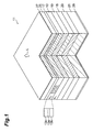
- Fig. 1 is a schematic view showing the structure of a nitride light generating device according to a first embodiment of the present invention
- Fig. 2 is a view showing fabrication steps for structures 1 and 2
- Fig. 3 is a view showing fabrication steps for structure 1
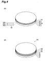
- Fig. 4 is a view showing fabrication steps for structure 2
- Fig. 5 is a schematic view showing a light emitting diode of the structure 1
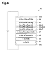
- Fig. 6 is a schematic view showing a light emitting diode of the structure 2
- Fig. 7 is a view showing the optical spectrums of the structure 1 measured at the temperatures of 300 K and 210K
- Fig. 8 is a view showing the optical spectrums of the structure 2 measured at the temperatures of 300 K and 210K
- Fig. 9 is a view showing a band diagram of the structure 1.
- Fig. 1 is a view showing the structure of a nitride semiconductor light generating device.
- the nitride semiconductor light generating device 11 comprises a quantum well active layer 13, an n-type gallium nitride based semiconductor 15, and a p-type AlGaN semiconductor layer 17.
- the quantum well active layer 13 includes an In X1 Al Y1 Ga 1-X1 - Y1 N (1>X1>0, 1>Y1>0) well layer 13a and an In X2 Al Y2 Ga 1-X2-Y2 N (1>X2>0, 1>Y2>0) barrier layer 13b.
- the nitride semiconductor light generating device 11 includes an InX 3 Al Y3 Ga 1-X3-Y3 N (1>X3>0, 1>Y3>0) layer 19.
- the In X3 Al Y3 Ga 1-X3-Y3 N (1>X3>0, 1>Y3>0) layer 19 is provided between the quantum well active layer 13 and the n-type gallium nitride based semiconductor layer 15.
- the p-type AlGaN layer 17 has the bandgap energy E CP greater than the bandgap energy E B of the In X2 Al Y2 Ga 1-X2-Y2 N barrier layer.13b.
- the quantum well active layer 13 is provided between the p-type AlGaN layer 17 and the In X3 Al Y3 Ga 1-X3-Y3 N layer 19.
- the indium composition X3 of the In X3 Al Y3 Ga 1-X3-Y3 N layer 19 is greater than the indium composition X1 of the In X1 Al Y1 Ga 1-X1-Y1 N well layer 13a.
- the indium composition X3 of the In X3 Al Y3 Ga 1-X3-Y3 N layer 19 is greater than the indium composition X2 of the In X2 Al Y2 Ga 1-X2-Y2 N barrier layer 13b.
- the aluminum composition Y1 of the In X1 Al Y1 Ga 1-X1-Y1 N well layer 13a is smaller than the aluminum composition Y3 of the In X3 Al Y3 Ga 1-X3-Y3 N layer 19.
- the aluminum composition Y2 of the In X2 Al Y2 Ga 1-X2-Y2 N barrier layer 13b is smaller than the aluminum composition Y3 of the In X3 Al Y3 Ga 1-X3-Y3 N layer 19.
- the oxygen concentration of the quantum well active layer 13 is lower than that of the In X3 Al Y3 Ga 1-X3-Y3 N layer 19.
- the In X3 Al Y3 Ga 1-X3-Y3 N layer 19 has an excellent buffering ability because the indium composition X3 of the In X3 Al Y3 Ga 1-X3-Y3 N layer 19 is greater than the indium composition X1 of the In X1 Al Y1 Ga 1-X1-Y1 N well layer 13a and the indium composition X3 of the In X3 Al Y3 Ga 1-X3-Y3 N layer 19 is greater than the indium composition X2 of the In X2 Al Y2 Ga 1-X2-Y2 N barrier layer 13b. Therefore, the optical performances and crystalline quality of the light generating quantum well layer 13 are improved.
- the indium composition X1 of the In X1 Al Y1 Ga 1-X1-Y1 N well layer 13a is smaller than the indium composition X3 of the In X3 Al Y3 Ga 1-X3-Y3 N layer 19 and the indium composition X2 of the In X2 Al Y2 Ga 1-X2-Y2 N barrier layer 13b is smaller than the indium composition X3 of the In X3 Al Y3 Ga 1-X3-Y3 N layer 19, the aluminum composition Y1 of the In X1 Al Y1 Ga 1-X1-Y1 N well layer 13a is decreased as compared to the aluminum composition Y3 of the In X3 Al Y3 Ga 1-X3-Y3 N layer 19, and the aluminum composition Y2 of the In X2 Al Y2 Ga 1-X2-Y2 N barrier layer 13b is decreased as compared to the aluminum composition Y3 of the In X3 Al Y3 Ga 1-X3-Y3 N layer 19, thereby providing the In X1 Al Y1 Ga 1-X1
- the aluminum composition Y1 of the In X1 Al Y1 Ga 1-X1-Y1 N well layer 13a and the aluminum composition Y2 of the In X2 Al Y2 Ga 1-X2-Y2 N barrier layer 13b are smaller than the aluminum composition Y3 of the In X3 Al Y3 Ga 1-X3-Y3 N layer 19, the oxygen concentration N 13 of the quantum well active layer 13 is lower than the oxygen concentration N 19 of the In X3 Al Y3 Ga 1-X3-Y3 N layer 19. Since the concentration of oxygen acting as n-type dopant is decreased in the quantum well active layer 13, electron leakage to the p-type AlGaN layer is reduced thereby enhancing the light emitting efficiency.
- the quantum well active layer 13 is provided to generate light in an ultraviolet wavelength region.
- the peak wavelength of the light is in the range of 260 nanometers to 360 nanometers. Since the quantum well active layer 13 has a quantum well structure, this quantum well structure is constituted to generate light of a desired wavelength in the ultraviolet wavelength region by adjusting bandgap energy widths and/or compositions of the well layer and barrier layer.
- the nitride semiconductor light generating device 11 further comprises a group III nitride substrate 21.
- the n-type gallium nitride based semiconductor 15 is provided between the In X3 Al Y3 Ga 1-X3-Y3 N layer 19 and the group III nitride substrate 21.
- group III nitride substrate 21 gallium nitride based semiconductor having an excellent crystalline quality is grown thereon.
- the group III nitride substrate 21 is an n-type gallium nitride substrate. Accordingly, the nitride semiconductor light generating device 11 is provided with a substrate having a low threading dislocation density.
- the nitride semiconductor light generating device 11 further comprises a buffer layer 23 provided on the group III nitride substrate 21.
- the buffer layer 23 is made of n-type gallium nitride based semiconductor.
- This n-type gallium nitride based semiconductor is, for example, n-type GaN or n-type AlGaN.
- the nitride semiconductor light generating device 11 further comprises a p-type gallium nitride based semiconductor layer 25 provided the p-type AlGaN layer 17.
- the p-type gallium nitride based semiconductor layer 25 has a bandgap energy smaller than that of the p-type AlGaN layer 17, and is made of, for example, p-type GaN or p-type AlGaN.
- the nitride semiconductor light generating device 11 further comprises a first electrode 27 provided the p-type gallium nitride based semiconductor layer 25, and a second electrode 29 provided on the back side of the group III nitride substrate 21.
- the first electrode 27 works as an anode electrode and the second electrode works as a cathode electrode.
- the oxygen concentration N 19 of the In X3 Al Y3 Ga 1-X3-Y3 N layer 19 be greater than or equal to 1 ⁇ 10 18 cm -3 .
- the oxygen concentration N 19 of the In X3 Al Y3 Ga 1-X3-Y3 N layer 19 be greater than or equal to 1 ⁇ 10 18 cm -3 .
- the oxygen concentration N 19 of the In X3 Al Y3 Ga 1-X3-Y3 N layer 19 be smaller than or equal to 1 ⁇ 10 20 cm -3 . If the oxygen concentration is greater than 1 ⁇ 10 20 cm -3 , the crystalline quality of the In X3 Al Y3 Ga 1-X3-Y3 N layer is deteriorated and this lowering affects the crystalline quality of the quantum well active layer 13.
- the oxygen concentration N 13 of the quantum well active layer 13 be smaller than 1 ⁇ 10 18 cm -3 . If the oxygen concentration of the quantum well active layer 13 is greater than or equal to 1 ⁇ 10 18 cm -3 , this affects the crystalline quality of the quantum well active layer 13 and also causes the increase of the electron leakage to the p-type AlGaN layer.
- the oxygen concentration N 13 of the quantum well active layer 13 be greater than or equal to 1 ⁇ 10 16 cm- 3 . If the oxygen concentration of the quantum well active layer 13 is lower than 1 ⁇ 10 16 cm -3 , the indium concentration is decreased and light generation efficiency is deteriorated.
- the oxygen concentration of the well layer 13a be lower than 1 ⁇ 10 18 cm -3 . If the well layer 13a has an oxygen concentration greater than or equal to 1 ⁇ 10 18 cm -3 , this affects the crystalline quality of the quantum well layer 13a and also causes the increase of the electron leakage to the p-type AlGaN layer.
- the oxygen concentration of the well layer 13a be greater than or equal to 1 ⁇ 10 16 cm -3 .
- the growth temperature has to be raised so that the oxygen concentration decreased below 1 ⁇ 10 16 cm -3 , and the indium concentration is lowered, thereby decreasing the light generation efficiency.
- the oxygen concentration of the barrier layer 13b be lower than 1 ⁇ 10 18 cm -3 . If the barrier layer 13b has an oxygen concentration greater than or equal to 1 ⁇ 10 18 cm -3 , this affects the crystalline quality of the barrier layer 13b and also causes the increase of the electron leakage to the p-type AlGaN layer.
- the oxygen concentration of the barrier layer 13b be greater than or equal to 1 ⁇ 10 16 cm -3 .
- the growth temperature has to be raised so that the oxygen concentration is decreased lower than 1 ⁇ 10 16 cm -3 , and the indium concentration of the barrier layer 13b is lowered, thereby decreasing the light generation efficiency.
- a gallium nitride wafer 31 is prepared.
- the gallium nitride wafer 31 has an electrical conductivity and is made of n-type GaN.
- the gallium nitride wafer 31 is set in an organo-metallic vapor phase epitaxy furnace, and a thermal cleaning of the gallium nitride wafer 31 is performed.
- the temperature of the organo-metallic vapor phase epitaxy furnace is set at the temperature of 1050 degrees Celsius.
- Gas containing ammonia and hydrogen (NH 3 + H 2 ) is supplied to the organo-metallic vapor phase epitaxy furnace to perform the thermal cleaning for ten minutes, for example.
- an n-type GaN film 33 is grown on the GaN wafer 31 using the organo-metallic vapor phase epitaxy furnace. This growth is performed at the temperature of 1150 degrees Celsius, for example, and the thickness of the n-type GaN film 33 is two micrometers, for example. Then, an n-type AlGaN film 35 is grown on the n-type GaN film 33. This growth is performed at the temperature of, for example, 1080 degrees Celsius.
- the composition of the n-type AlGaN film 35 is, for example, Al 0.18 Ga 0.82 N, and the thickness of the n-type AlGaN film 35 is, for example, 30 nanometers.
- an n-type InAlGaN buffer layer 37 (hereinafter referred to as the In X3 Al Y3 Ga 1-X3-Y3 N (1 > X3 >0, 1 > Y3 >0) as with the first embodiment) is grown on the n-type AlGaN film 35.
- the growth is performed at the temperature of 780 degrees Celsius, for example.
- the composition of the n-type InAlGaN buffer layer 37 is, for example, In 0.05 Al 0.24 Ga 0.71 N, and its thickness is, for example, 35 nanometers.
- a quantum well active region 39 for structure 1 is grown on the epitaxial wafer "B."
- the quantum well active region 39 includes a well layer 39a and a barrier layer 39b.
- the well layer 39a is an In U1 Al V1 Ga 1-U1-V1 N (1 > U1 >0, 1 > V1 >0).
- the barrier layer 39b is an In U2 Al V2 Ga 1-U2-V2 N (1 > U2 >0, 1 > V2 >0).
- the formation temperature of the quantum well active region 39 is substantially the same as the growth temperature of the InAlGaN buffering layer 37.
- the growth of the quantum well active region 39 is performed at the temperature of 780 degrees Celsius.
- the composition of the well layer 39a is In 0.06 Al 0.19 Ga 0.75 N and the composition of the barrier layer 39b is In 0.05 Al 0.24 Ga 0.71 N.
- the thickness of the In 0.06 Al 0.19 Ga 0.75 N well layer is 2.5 nanometers and the thickness of the In 0.05 Al 0.24 Ga 0.71 N barrier layer is 15 nanometers.
- a p-type AlGaN film 41 for blocking electrons is formed using the organo-metallic vapor phase epitaxy furnace. This growth is performed at the temperature of 1030 degrees Celsius, for example.
- the composition of the p-type AlGaN film 41 is, for example, Al 0.27 Ga 0.73 N and the thickness of the p-type AlGaN film 41 is, for example, 25 nanometers.
- a p-type AlGaN film 43 for forming an excellent ohmic contact is grown using the organo-metallic vapor phase epitaxy furnace. This growth is performed at the temperature of 1030 degrees Celsius.
- the composition of the p-type AlGaN film 43 is, for example, Al 0.18 Ga 0.82 N and the thickness of the p-type AlGaN film 43 is, for example, 60 nanometers. These steps provide an epitaxial wafer "B1."
- a quantum well active region 45 for structure 2 is grown on the epitaxial wafer "B."
- the quantum well active region 45 includes a well layer 45a and a barrier layer 45b.
- the well layer 45a is an In X1 Al Y1 Ga 1-X1-Y1 N (1 > X1 >0, 1 > Y1 >0).
- the barrier layer 45b is an In X2 Al Y2 Ga 1-X2-Y2 N (1 > X2 >0, 1 > Y2 >0).
- the formation temperature of the quantum well active region 45 is higher than the growth temperature of the InAlGaN buffering layer 37. In the present embodiment, the growth of the quantum well active region 45 is performed at the temperature of 830 degrees Celsius.
- the indium composition X3 of the In X3 Al Y3 Ga 1-X3 - Y3 N layer is greater than the indium composition X1 of the In X1 Al Y1 Ga 1-X1-Y1 N well layer, and the indium composition X3 of the In X3 Al Y3 Ga 1-X3 - Y3 N layer is greater than the indium composition X2 of the In X2 Al Y2 Ga 1 - X2-Y2 N barrier layer.
- the aluminum composition Y1 of the Inx 1 Al Y1 Ga 1-X1-Y1 N well layer is smaller than the aluminum composition Y3 of the In X3 Al Y3 Ga 1-X3-Y3 N layer
- the aluminum composition Y2 of the In X2 Al Y2 Ga 1-X2-Y2 N barrier layer is smaller than the aluminum composition Y3 of the In X3 Al Y3 Ga 1-X3-Y3 N layer.
- the composition of the well layer 45a is In 0.02 Al 0.09 Ga 0.81 N and the composition of the barrier layer 45b is In 0.02 Al 0.22 Ge 0.76 N.
- the thickness of the In 0.02 Al 0.09 Ga 0.81 N well layer is 2.7 nanometers and the thickness of the In 0.02 Al 0.22 Ga 0.76 N barrier layer is 15 nanometers.
- a p-type AlGaN film 47 is formed using the organo-metallic vapor phase epitaxy furnace. This growth is performed at the temperature of 1030 degrees Celsius, for example.
- the composition of the p-type AlGaN film 47 is, for example, Al 0.27 Ga 0.73 N and the thickness of the p-type AlGaN film 47 for blocking electrons is, for example, 25 nanometers.
- a p-type AlGaN film 49 for forming an excellent ohmic contact is grown using the organo-metallic vapor phase epitaxy furnace. This growth is performed at the temperature of 1030 degrees Celsius.
- composition of the p-type AlGaN film 49 is, for example, Al 1.18 Ga 0.82 N and the thickness of the p-type AIGaN film 49 is, for example, 60 nanometers. These steps provide an epitaxial wafer "B2.”
- the epitaxial substrates "B1" and “B2” are analyzed by SIMS method to estimate the oxygen concentrations of the quantum well active layers 39, 45.
- the oxygen concentrations of the quantum well active layer 39 and buffering layer in the epitaxial substrate “B1” both are about 1 ⁇ 10 18 cm -3 .
- the oxygen concentrations of the quantum well active layer 45 and buffering layer in the epitaxial substrate “B2” are about 5 ⁇ 10 17 cm -3 and about 1 ⁇ 10 18 cm -3 , respectively. This shows that the oxygen concentration is reduced by increase the growth temperature of AlInGaN. The reduction of oxygen concentrations provides the excellent crystal quality.
- An anode electrode 51 a such as Ni/Au
- a cathode electrode 51b such as Ti/Al
- An anode electrode 53a such as Ni/Au
- a cathode electrode 53b such as Ti/A1
- the above board signal in the emission spectrum of the LED structure "S1" comes from emission by the p-type AlGaN region.
- the efficiency of this emission is not strong at room temperature. But, as the temperature is lowered, this emission efficiency becomes high and the electrical characteristics of the p-type AlGaN region are deteriorated, thereby causing the leakage of electron from the quantum well active region.
- the emission from the leakage of electron appears in the emission spectrum of the LED structure "S 1."
- the emission spectrum of the LED structure "S2" does not have any board signal as above. That is, as shown in Fig.
- the leakage "E1" of electron is increased in the quantum well active layer having a high oxygen concentration, and this deteriorates the injection efficiency because oxygen acts as donor in the gallium nitride based semiconductor.
- the recombination of electrons "E1" and holes “H1" in the quantum well active layer generates light having a wavelength component of 350 nanometers (ultraviolet light).
- the recombination of electrons E2 and holes H2 in the quantum well active layer generates light having a wavelength component of 390 nanometers.
- This emission relates to deep acceptor level form magnesium (Mg) and appears as a board signal in the emission spectrum around 390 nanometers.
- the peak intensity of the LED structure "S2" is twice as high as that of the LED structure "S1.” This comes from the following:
Abstract
Description
- The present invention relates to a nitride semiconductor light generating device.
- Patent Publication 1 (
Japanese Patent Application Laid Open No. 2000-164925 - In the nitride light generating device of Patent Publication 1, the active layer of the oxygen atom concentration Qa is sandwiched by the n-type cladding layer of the oxygen atom concentration Qc and the p-type cladding layer of the oxygen atom concentration Qp. Patent Publication 1 does not provide any teaching of the active layer including an InAlGaN semiconductor layer.
- It is an object to provide a nitride semiconductor light generating device, which has a high carrier injection efficiency, including an active layer having an InAlGaN semiconductor layer.
- According to one aspect of the present invention, a nitride semiconductor light generating device comprises: (a) an n-type gallium nitride based semiconductor layer; (b) a quantum well active layer including an InX1AlY1Ga1-X1-Y1N (1>X1>0, 1>Y1>0) well layer and an InX2AlY2Ga1-X2-Y2N (1>X2>0, 1>Y2>0) barrier layer; (c) an InX3AlY3Ga1-X3-Y3N (1>X3>0, 1>Y3>0) layer provided between the quantum well active layer and the n-type gallium nitride based semiconductor layer, an indium composition X3 of the InX3AlY3Ga1-X3-Y3N layer being greater than an indium composition X1 of the InX1AlY1Ga1-X1-Y1N well layer, an indium composition X3 of the InX3AlY3Ga1-X3-Y3N layer being greater than an indium composition X2 of the InX2AlY2Ga1-X2-Y2N barrier layer, an aluminum composition Y1 of the InX1AlY1Ga1-X1-Y1N well layer being smaller than an aluminum composition Y3 of the InX3AlY3Ga1-X3-Y3N layer, an aluminum composition Y2 of the InX2AlY2Ga1-X2-Y2N barrier layer being smaller than an aluminum composition Y3 of the InX3AlY3Ga1-X3-Y3N layer, and an oxygen concentration of the quantum well active layer being lower than that of the InX3AlY3Ga1-X3-Y3N layer; and (d) a p-type AlGaN layer having a bandgap energy greater than that of the InX2AlY2Ga1-X2-Y2N barrier layer, the quantum well active layer being provided between the p-type AlGaN layer and the InX3AlY3Ga1-X3-Y3N layer.
- In the nitride semiconductor light generating device, the InX3AlY3Ga1-X3-Y3N layer has an excellent buffering ability because the indium composition X3 of the InX3AlY3Ga1-X3-Y3N layer is greater than the indium composition X1 of the InX1AlY1Ga1-X1-Y1N well layer and is greater than the indium composition X2 of the InX2AlY2Ga1-X2-Y2N barrier layer. Therefore, the light generating quantum well layer has an excellent crystalline quality.
- Further, since the indium composition X1 of the InX1AlY1Ga1-X1-Y1N well layer is smaller than the indium composition X3 of the InX3AlY3Ga1-X3-Y3N layer and the indium composition X2 of the InX2AlY2Ga1-X2-Y2N barrier layer is smaller than the indium composition X3 of the InX3AlY3Ga1-X3-Y3N layer, the aluminum composition Y1 of the InX1AlY1Ga1-X1-Y1
N well layer 13a is decreased as compared to the aluminum composition Y3 of the InX3AlY3Ga1-X3-Y3N layer. The aluminum composition Y2 of the InX2AlY2Ga1-X2-Y2N barrier layer is decreased as compared to the aluminum composition Y3 of the InX3AlY3Ga1-X3-Y3N layer to obtain the InX1AlY1Ga1-X1-Y1N well layer and InX2AlY2Ga1-X2-Y2N well layer each having the desired value of bandgap energy. - Furthermore, since the aluminum composition Y1 of the InX1AlY1Ga1-X1-Y1N well layer and the aluminum composition Y2 of the InX2AlY2Ga1-X2-Y2N barrier layer is smaller than the aluminum composition Y3 of the InX3AlY3Ga1-X3-Y3N layer, the oxygen concentration of the quantum well active layer is lowered as compared to the oxygen concentration of the InX3AlY3Ga1-X3-Y3N layer.
- Since the concentration of oxygen acting as n-type dopant is decreased, electron leakage to the p-type AlGaN layer is reduced, so that the light emitting efficiency is enhanced.
- In the nitride semiconductor light generating device according to the present invention, it is preferable that an oxygen concentration of the InX3AlY3Ga1-X3-Y3N layer be greater than or equal to 1 × 1018 cm-3. In order to lower the oxygen concentration below 1 × 1018 cm-3, it is necessary to raise the growth temperature to lower the indium concentration of the InX3AlY3Ga1-X3-Y3N layer, but if the indium concentration is lower that 1 × 1018 cm-3, the buffering ability of the InX3AlY3Ga1-X3-Y3N layer is deteriorated.
- In the nitride semiconductor light generating device according to the present invention, it is preferable that an oxygen concentration of the InX3AlY3Ga1-X3-Y3N layer be lower than or equal to 1 × 1020 cm-3. If this oxygen concentration is increased above 1 × 1020 cm-3, the crystalline quality of the InX3AlY3Ga1-X3-Y3N layer is lowered and this lowering affects the crystalline quality of the quantum well active layer.
- In the nitride semiconductor light generating device according to the present invention, it is preferable that an oxygen concentration of the quantum well active layer be lower than 1 × 1018 cm-3. If the well layer has an oxygen concentration greater than or equal to 1 × 1018 cm-3, this affects its crystalline quality and the electron leakage to the p-type AlGaN layer is increased.
- In the nitride semiconductor light generating device according to the present invention, it is preferable that an oxygen concentration of the quantum well active layer be greater than or equal to 1 × 1016 cm-3. The growth temperature has to be raised to obtain the oxygen concentration lower than 1 × 1016 cm-3, and the indium concentration of the quantum well active layer is lowered thereby deteriorating the light generation efficiency.
- The nitride semiconductor light generating device according to the present invention further comprises a group III nitride substrate, and the n-type gallium nitride based semiconductor layer is provided between the InX3AlY3Ga1-X3-Y3N layer and the group III nitride substrate. By use of the group III
nitride substrate 21, gallium nitride based semiconductor having an excellent crystalline quality can be grown thereon. - In the nitride semiconductor light generating device according to the present invention, it is preferable that the group III nitride substrate include a gallium nitride substrate.
- The above objects and other objects, features, and advantages of the present invention will be understood easily from the following detailed description of the preferred embodiments of the present invention with reference to the accompanying drawings.
- Fig. 1 is a schematic view showing the structure of a nitride light generating device according to a first embodiment of the present invention;
Fig. 2 is a view showing fabrication steps for structures 1 and 2;
Fig. 3 is a view showing fabrication steps for structure 1;
Fig. 4 is a view showing fabrication steps for structure 2;
Fig. 5 is a schematic view showing a light emitting diode of the structure 1;
Fig. 6 is a schematic view showing a light emitting diode of the structure 2;
Fig. 7 is a view showing the optical spectrums of the structure 1 measured at the temperatures of 300 K and 210K;
Fig. 8 is a view showing the optical spectrums of the structure 2 measured at the temperatures of 300 K and 210K; and
Fig. 9 is a view showing a band diagram of the structure 1. - The teachings of the present invention will readily be understood in view of the following detailed description with reference to the accompanying drawings illustrated by way of example. Referring to the accompanying drawings, embodiments of the present invention will be explained. When possible, parts identical to each other will be referred to with symbols identical to each other.
- Fig. 1 is a view showing the structure of a nitride semiconductor light generating device. The nitride semiconductor
light generating device 11 comprises a quantum wellactive layer 13, an n-type gallium nitride basedsemiconductor 15, and a p-typeAlGaN semiconductor layer 17. The quantum wellactive layer 13 includes an InX1AlY1Ga1-X1-Y1N (1>X1>0, 1>Y1>0)well layer 13a and an InX2AlY2Ga1-X2-Y2N (1>X2>0, 1>Y2>0)barrier layer 13b. The nitride semiconductorlight generating device 11 includes an InX3AlY3Ga1-X3-Y3N (1>X3>0, 1>Y3>0)layer 19. The InX3AlY3Ga1-X3-Y3N (1>X3>0, 1>Y3>0)layer 19 is provided between the quantum wellactive layer 13 and the n-type gallium nitride basedsemiconductor layer 15. The p-type AlGaN layer 17 has the bandgap energy ECP greater than the bandgap energy EB of the InX2AlY2Ga1-X2-Y2N barrier layer.13b. The quantum wellactive layer 13 is provided between the p-type AlGaN layer 17 and the InX3AlY3Ga1-X3-Y3N layer 19. The indium composition X3 of the InX3AlY3Ga1-X3-Y3N layer 19 is greater than the indium composition X1 of the InX1AlY1Ga1-X1-Y1N well layer 13a. The indium composition X3 of the InX3AlY3Ga1-X3-Y3N layer 19 is greater than the indium composition X2 of the InX2AlY2Ga1-X2-Y2N barrier layer 13b. The aluminum composition Y1 of the InX1AlY1Ga1-X1-Y1N well layer 13a is smaller than the aluminum composition Y3 of the InX3AlY3Ga1-X3-Y3N layer 19. The aluminum composition Y2 of the InX2AlY2Ga1-X2-Y2N barrier layer 13b is smaller than the aluminum composition Y3 of the InX3AlY3Ga1-X3-Y3N layer 19. The oxygen concentration of the quantum wellactive layer 13 is lower than that of the InX3AlY3Ga1-X3-Y3N layer 19. - In the nitride semiconductor
light generating device 11, the InX3AlY3Ga1-X3-Y3N layer 19 has an excellent buffering ability because the indium composition X3 of the InX3AlY3Ga1-X3-Y3N layer 19 is greater than the indium composition X1 of the InX1AlY1Ga1-X1-Y1N well layer 13a and the indium composition X3 of the InX3AlY3Ga1-X3-Y3N layer 19 is greater than the indium composition X2 of the InX2AlY2Ga1-X2-Y2N barrier layer 13b. Therefore, the optical performances and crystalline quality of the light generatingquantum well layer 13 are improved. - Since the indium composition X1 of the InX1AlY1Ga1-X1-Y1
N well layer 13a is smaller than the indium composition X3 of the InX3AlY3Ga1-X3-Y3N layer 19 and the indium composition X2 of the InX2AlY2Ga1-X2-Y2N barrier layer 13b is smaller than the indium composition X3 of the InX3AlY3Ga1-X3-Y3N layer 19, the aluminum composition Y1 of the InX1AlY1Ga1-X1-Y1N well layer 13a is decreased as compared to the aluminum composition Y3 of the InX3AlY3Ga1-X3-Y3N layer 19, and the aluminum composition Y2 of the InX2AlY2Ga1-X2-Y2N barrier layer 13b is decreased as compared to the aluminum composition Y3 of the InX3AlY3Ga1-X3-Y3N layer 19, thereby providing the InX1AlY1Ga1-X1-Y1N well layer 13a and the InX2AlY2Ga1-X2-Y2N welllayer 13b each having the desired value of bandgap energy. - Furthermore, since the aluminum composition Y1 of the InX1AlY1Ga1-X1-Y1
N well layer 13a and the aluminum composition Y2 of the InX2AlY2Ga1-X2-Y2N barrier layer 13b are smaller than the aluminum composition Y3 of the InX3AlY3Ga1-X3-Y3N layer 19, the oxygen concentration N13 of the quantum wellactive layer 13 is lower than the oxygen concentration N19 of the InX3AlY3Ga1-X3-Y3N layer 19. Since the concentration of oxygen acting as n-type dopant is decreased in the quantum wellactive layer 13, electron leakage to the p-type AlGaN layer is reduced thereby enhancing the light emitting efficiency. - In the nitride semiconductor
light generating device 11, the quantum wellactive layer 13 is provided to generate light in an ultraviolet wavelength region. Preferably, the peak wavelength of the light is in the range of 260 nanometers to 360 nanometers. Since the quantum wellactive layer 13 has a quantum well structure, this quantum well structure is constituted to generate light of a desired wavelength in the ultraviolet wavelength region by adjusting bandgap energy widths and/or compositions of the well layer and barrier layer. - The nitride semiconductor
light generating device 11 further comprises a group IIInitride substrate 21. The n-type gallium nitride basedsemiconductor 15 is provided between the InX3AlY3Ga1-X3-Y3N layer 19 and the groupIII nitride substrate 21. By using groupIII nitride substrate 21, gallium nitride based semiconductor having an excellent crystalline quality is grown thereon. Preferably, the groupIII nitride substrate 21 is an n-type gallium nitride substrate. Accordingly, the nitride semiconductorlight generating device 11 is provided with a substrate having a low threading dislocation density. - The nitride semiconductor
light generating device 11 further comprises abuffer layer 23 provided on the groupIII nitride substrate 21. Thebuffer layer 23 is made of n-type gallium nitride based semiconductor. This n-type gallium nitride based semiconductor is, for example, n-type GaN or n-type AlGaN. - The nitride semiconductor
light generating device 11 further comprises a p-type gallium nitride based semiconductor layer 25 provided the p-type AlGaN layer 17. The p-type gallium nitride based semiconductor layer 25 has a bandgap energy smaller than that of the p-type AlGaN layer 17, and is made of, for example, p-type GaN or p-type AlGaN. - The nitride semiconductor
light generating device 11 further comprises afirst electrode 27 provided the p-type gallium nitride based semiconductor layer 25, and asecond electrode 29 provided on the back side of the groupIII nitride substrate 21. Thefirst electrode 27 works as an anode electrode and the second electrode works as a cathode electrode. When voltage is applied across the anode electrode and the cathode electrode, then carries are injected into the quantum wellactive layer 13 to generate light "L" in response to the recombination of the carriers. - In the nitride semiconductor
light generating device 11, it is preferable that the oxygen concentration N19 of the InX3AlY3Ga1-X3-Y3N layer 19 be greater than or equal to 1 × 1018 cm-3. In order to lower the oxygen concentration below 1 × 1018 cm-3, it is necessary to raise the growth temperature, and this causes the decrease of the indium composition and the resulting deterioration of the buffering ability of the InX3AlY3Ga1-X3-Y3N layer 19. - In the nitride semiconductor
light generating device 11, it is preferable that the oxygen concentration N19 of the InX3AlY3Ga1-X3-Y3N layer 19 be smaller than or equal to 1 × 1020 cm-3. If the oxygen concentration is greater than 1 × 1020 cm-3, the crystalline quality of the InX3AlY3Ga1-X3-Y3N layer is deteriorated and this lowering affects the crystalline quality of the quantum wellactive layer 13. - In the nitride semiconductor
light generating device 11, it is preferable that that the oxygen concentration N13 of the quantum wellactive layer 13 be smaller than 1 × 1018 cm-3. If the oxygen concentration of the quantum wellactive layer 13 is greater than or equal to 1 × 1018 cm-3, this affects the crystalline quality of the quantum wellactive layer 13 and also causes the increase of the electron leakage to the p-type AlGaN layer. - In the nitride semiconductor
light generating device 11, it is preferable that the oxygen concentration N13 of the quantum wellactive layer 13 be greater than or equal to 1 × 1016 cm-3. If the oxygen concentration of the quantum wellactive layer 13 is lower than 1 × 1016 cm-3, the indium concentration is decreased and light generation efficiency is deteriorated. - Further, in the nitride semiconductor
light generating device 11, it is preferable that the oxygen concentration of thewell layer 13a be lower than 1 × 1018 cm-3. If thewell layer 13a has an oxygen concentration greater than or equal to 1 × 1018 cm-3, this affects the crystalline quality of thequantum well layer 13a and also causes the increase of the electron leakage to the p-type AlGaN layer. - In the nitride semiconductor
light generating device 11, it is preferable that that the oxygen concentration of thewell layer 13a be greater than or equal to 1 × 1016 cm-3. The growth temperature has to be raised so that the oxygen concentration decreased below 1 × 1016 cm-3, and the indium concentration is lowered, thereby decreasing the light generation efficiency. - Furthermore, in the nitride semiconductor
light generating device 11, it is preferable that the oxygen concentration of thebarrier layer 13b be lower than 1 × 1018 cm-3. If thebarrier layer 13b has an oxygen concentration greater than or equal to 1 × 1018 cm-3, this affects the crystalline quality of thebarrier layer 13b and also causes the increase of the electron leakage to the p-type AlGaN layer. - In the nitride semiconductor
light generating device 11, it is preferable that that the oxygen concentration of thebarrier layer 13b be greater than or equal to 1 × 1016 cm-3. The growth temperature has to be raised so that the oxygen concentration is decreased lower than 1 × 1016 cm-3, and the indium concentration of thebarrier layer 13b is lowered, thereby decreasing the light generation efficiency. - With reference to Parts (A) and (B) of Fig. 2 and Parts (A) and (B) of Fig. 3, a method of fabricating a nitride semiconductor light generating device will be explained. A
gallium nitride wafer 31 is prepared. Thegallium nitride wafer 31 has an electrical conductivity and is made of n-type GaN. Thegallium nitride wafer 31 is set in an organo-metallic vapor phase epitaxy furnace, and a thermal cleaning of thegallium nitride wafer 31 is performed. For this thermal cleaning, the temperature of the organo-metallic vapor phase epitaxy furnace is set at the temperature of 1050 degrees Celsius. Gas containing ammonia and hydrogen (NH3+ H2) is supplied to the organo-metallic vapor phase epitaxy furnace to perform the thermal cleaning for ten minutes, for example. - Thereafter, as shown in Part (A) of Fig. 2, an n-
type GaN film 33 is grown on theGaN wafer 31 using the organo-metallic vapor phase epitaxy furnace. This growth is performed at the temperature of 1150 degrees Celsius, for example, and the thickness of the n-type GaN film 33 is two micrometers, for example. Then, an n-type AlGaN film 35 is grown on the n-type GaN film 33. This growth is performed at the temperature of, for example, 1080 degrees Celsius. The composition of the n-type AlGaN film 35 is, for example, Al0.18Ga0.82N, and the thickness of the n-type AlGaN film 35 is, for example, 30 nanometers. - As shown in Part (B) of Fig. 2, an n-type InAlGaN buffer layer 37 (hereinafter referred to as the InX3AlY3Ga1-X3-Y3N (1 > X3 >0, 1 > Y3 >0) as with the first embodiment) is grown on the n-
type AlGaN film 35. The growth is performed at the temperature of 780 degrees Celsius, for example. The composition of the n-typeInAlGaN buffer layer 37 is, for example, In0.05Al0.24Ga0.71N, and its thickness is, for example, 35 nanometers. These steps provide an epitaxial wafer "B." - Next, with reference to Parts (A) and (B) of Fig. 3, the formation of a quantum well active region will be explained. First, a quantum well
active region 39 for structure 1 is grown on the epitaxial wafer "B." The quantum wellactive region 39 includes awell layer 39a and abarrier layer 39b. Thewell layer 39a is an InU1AlV1Ga1-U1-V1N (1 > U1 >0, 1 > V1 >0). Thebarrier layer 39b is an InU2AlV2Ga1-U2-V2N (1 > U2 >0, 1 > V2 >0). The formation temperature of the quantum wellactive region 39 is substantially the same as the growth temperature of theInAlGaN buffering layer 37. In the present embodiment, the growth of the quantum wellactive region 39 is performed at the temperature of 780 degrees Celsius. In one example, the composition of thewell layer 39a is In0.06Al0.19Ga0.75N and the composition of thebarrier layer 39b is In0.05Al0.24Ga0.71N. The thickness of the In0.06Al0.19Ga0.75N well layer is 2.5 nanometers and the thickness of the In0.05Al0.24Ga0.71N barrier layer is 15 nanometers. - As shown in Part (B) of Fig. 3, a p-
type AlGaN film 41 for blocking electrons is formed using the organo-metallic vapor phase epitaxy furnace. This growth is performed at the temperature of 1030 degrees Celsius, for example. The composition of the p-type AlGaN film 41 is, for example, Al0.27Ga0.73N and the thickness of the p-type AlGaN film 41 is, for example, 25 nanometers. Then, a p-type AlGaN film 43 for forming an excellent ohmic contact is grown using the organo-metallic vapor phase epitaxy furnace. This growth is performed at the temperature of 1030 degrees Celsius. The composition of the p-type AlGaN film 43 is, for example, Al0.18Ga0.82N and the thickness of the p-type AlGaN film 43 is, for example, 60 nanometers. These steps provide an epitaxial wafer "B1." - With reference to Parts (A) and (B) of Fig. 4, a quantum well
active region 45 for structure 2 is grown on the epitaxial wafer "B." The quantum wellactive region 45 includes awell layer 45a and abarrier layer 45b. Thewell layer 45a is an InX1AlY1Ga1-X1-Y1N (1 > X1 >0, 1 > Y1 >0). Thebarrier layer 45b is an InX2AlY2Ga1-X2-Y2N (1 > X2 >0, 1 > Y2 >0). The formation temperature of the quantum wellactive region 45 is higher than the growth temperature of theInAlGaN buffering layer 37. In the present embodiment, the growth of the quantum wellactive region 45 is performed at the temperature of 830 degrees Celsius. The indium composition X3 of the InX3AlY3Ga1-X3-Y3N layer is greater than the indium composition X1 of the InX1AlY1Ga1-X1-Y1N well layer, and the indium composition X3 of the InX3AlY3Ga1-X3-Y3N layer is greater than the indium composition X2 of the InX2AlY2Ga1-X2-Y2N barrier layer. The aluminum composition Y1 of the Inx1AlY1Ga1-X1-Y1N well layer is smaller than the aluminum composition Y3 of the InX3AlY3Ga1-X3-Y3N layer, and the aluminum composition Y2 of the InX2AlY2Ga1-X2-Y2N barrier layer is smaller than the aluminum composition Y3 of the InX3AlY3Ga1-X3-Y3N layer. In one example, the composition of thewell layer 45a is In0.02Al0.09Ga0.81N and the composition of thebarrier layer 45b is In0.02Al0.22Ge0.76N. The thickness of the In0.02Al0.09Ga0.81N well layer is 2.7 nanometers and the thickness of the In0.02Al0.22Ga0.76N barrier layer is 15 nanometers. - As shown in Part (B) of Fig. 4, a p-
type AlGaN film 47 is formed using the organo-metallic vapor phase epitaxy furnace. This growth is performed at the temperature of 1030 degrees Celsius, for example. The composition of the p-type AlGaN film 47 is, for example, Al0.27Ga0.73N and the thickness of the p-type AlGaN film 47 for blocking electrons is, for example, 25 nanometers. Then, a p-type AlGaN film 49 for forming an excellent ohmic contact is grown using the organo-metallic vapor phase epitaxy furnace. This growth is performed at the temperature of 1030 degrees Celsius. The composition of the p-type AlGaN film 49 is, for example, Al1.18Ga0.82N and the thickness of the p-type AIGaN film 49 is, for example, 60 nanometers. These steps provide an epitaxial wafer "B2." - The epitaxial substrates "B1" and "B2" are analyzed by SIMS method to estimate the oxygen concentrations of the quantum well
active layers active layer 39 and buffering layer in the epitaxial substrate "B1" both are about 1 × 1018 cm-3. The oxygen concentrations of the quantum wellactive layer 45 and buffering layer in the epitaxial substrate "B2" are about 5 × 1017 cm-3 and about 1 × 1018 cm-3, respectively. This shows that the oxygen concentration is reduced by increase the growth temperature of AlInGaN. The reduction of oxygen concentrations provides the excellent crystal quality. - An
anode electrode 51 a, such as Ni/Au, is formed on the p-type region of the epitaxial wafer B1 and acathode electrode 51b, such as Ti/Al, is formed on the backside of the GaN substrate in the epitaxial wafer "B1" to form an LED structure "S1" as shown in Fig. 5. Ananode electrode 53a, such as Ni/Au, is formed on the p-type region in the epitaxial wafer "B2" and acathode electrode 53b, such as Ti/A1, is formed on the backside of the GaN substrate in the epitaxial wafer "B2" to form an LED structure "S2" as shown in Fig. 6. - Voltages are applied to these LED structures "S1," "S2" to measure optical power. Parts (A) and (B) of Fig. 7 show emission spectrums of the LED structure "S1." Parts (A) and (B) of Fig. 8 show emission spectrums of the LED structure "S2." The emission spectrums in Parts (A) of Figs. 7 and 8 are measured at the temperature of 300 Kelvin and the emission spectrums in Parts (B) of Figs. 7 and 8 are measured at the temperature of 210 Kelvin. Each of the emission spectrums of the LED structures "S1" and "S2" has a single sharp peak. But, the emission spectrum of the LED structure "S1" has an additional board signal indicating another emission in wavelength region longer than the peak wavelength at the temperature of 210 Kelvin.
- It is thought that the above board signal in the emission spectrum of the LED structure "S1" comes from emission by the p-type AlGaN region. The efficiency of this emission is not strong at room temperature. But, as the temperature is lowered, this emission efficiency becomes high and the electrical characteristics of the p-type AlGaN region are deteriorated, thereby causing the leakage of electron from the quantum well active region. The emission from the leakage of electron appears in the emission spectrum of the LED structure "S 1." The emission spectrum of the LED structure "S2" does not have any board signal as above. That is, as shown in Fig. 9, the leakage "E1" of electron is increased in the quantum well active layer having a high oxygen concentration, and this deteriorates the injection efficiency because oxygen acts as donor in the gallium nitride based semiconductor. The recombination of electrons "E1" and holes "H1" in the quantum well active layer generates light having a wavelength component of 350 nanometers (ultraviolet light). The recombination of electrons E2 and holes H2 in the quantum well active layer generates light having a wavelength component of 390 nanometers. This emission relates to deep acceptor level form magnesium (Mg) and appears as a board signal in the emission spectrum around 390 nanometers.
- The peak intensity of the LED structure "S2" is twice as high as that of the LED structure "S1." This comes from the following:
- (1) When the growth temperatures of the well and barrier layers are raised, abruptness of the interface between the well and barrier layers becomes excellent.
- (2) When the growth temperatures of the well and barrier layers are raised, the quantity of oxygen taken therein is reduced, thereby improving the crystal quality of the quantum well active layer.
- (3) When the oxygen concentration is small, the carrier injection efficiency is improved.
Therefore, most of electrons E are recombined with holes H in the quantum well active layer and thus the intensity of light (ultraviolet) having a wavelength component of 350 nm becomes strong. Accordingly, The quantity of holes "H" and electrons "E" recombined in the p-type AIGaN region becomes small. - Having described and illustrated the principle of the invention in a preferred embodiment thereof, it is appreciated by those having skill in the art that the invention can be modified in arrangement and detail without departing from such principles. We therefore claim all modifications and variations coming within the spirit and scope of the following claims.
Claims (7)
- A nitride semiconductor light generating device comprising:an n-type gallium nitride based semiconductor layer;a quantum well active layer including an InX1AlY1,Ga1-X1-Y1N (1>X1>0, 1>Y1>0) well layer and an InX2AlY2Ga1-X2-Y2N (1>X2>0, 1>Y2>0) barrier layer;an InX3AlY3Ga1-X3-Y3N (1>X3>0, 1>Y3>0) layer provided between the quantum well active layer and the n-type gallium nitride based semiconductor layer, an indium composition X3 of the InX3AlY3Ga1-X3-Y3N layer being greater than an indium composition X1 of the InX1AlY1Ga1-X1-Y1N well layer, an indium composition X3 of the InX3AlY3Ga1-X3-Y3N layer being greater than an indium composition X2 of the InX2AlY2Ga1-X2-Y2N barrier layer, an aluminum composition Y1 of the InX1AlY1Ga1-X1-Y1N well layer being smaller than an aluminum composition Y3 of the InX3AlY3Ga1-X3-Y3N layer, an aluminum composition Y2 of the InX2AlY2Ga1-X2-Y2N barrier layer being smaller than an aluminum composition Y3 of the InX3AlY3Ga1-X3-Y3N layer, and an oxygen concentration of the quantum well active layer being lower than that of the InX3AlY3Ga1-X3-Y3N layer; anda p-type AlGaN layer having a bandgap energy greater than that of the InX2AlY2Ga1-X2-Y2N barrier layer, the quantum well active layer being provided between the p-type AlGaN layer and the InX3AlY3Ga1-X3-Y3N layer.
- The nitride semiconductor light generating device according to claim 1, wherein an oxygen concentration of the InX3AlY3Ga1-X3,Y3N layer is greater than or equal to 1 × 1018 cm-3.
- The nitride semiconductor light generating device according to claim 1 or claim 2, wherein an oxygen concentration of the InX3AlY3Ga1-X3-Y3N layer is lower than or equal to 1 × 1020 cm-3.
- The nitride semiconductor light generating device according to claim 1, claim 2 or claim 3, wherein an oxygen concentration of the quantum well active layer is lower than 1 × 1018 cm-3.
- The nitride semiconductor light generating device according to claim 1, claim 2, claim 3 or claim 4, wherein an oxygen concentration of the quantum well active layer is greater than or equal to 1 × 1016 cm-3.
- The nitride semiconductor light generating device according to claim 1, claim 2, claim 3, claim 4 or claim 5, further comprising a group III nitride substrate, the n-type gallium nitride based semiconductor layer being provided between the InX3AIY3Ga1-X3-Y3N layer and the group III nitride substrate.
- The nitride semiconductor light generating device according to claim 6, wherein the group III nitride substrate includes a gallium nitride substrate.
Applications Claiming Priority (1)
| Application Number | Priority Date | Filing Date | Title |
|---|---|---|---|
| JP2006018159A JP2007201195A (en) | 2006-01-26 | 2006-01-26 | Nitride semiconductor light emitting device |
Publications (2)
| Publication Number | Publication Date |
|---|---|
| EP1814164A2 true EP1814164A2 (en) | 2007-08-01 |
| EP1814164A3 EP1814164A3 (en) | 2008-11-05 |
Family
ID=37897738
Family Applications (1)
| Application Number | Title | Priority Date | Filing Date |
|---|---|---|---|
| EP07001335A Withdrawn EP1814164A3 (en) | 2006-01-26 | 2007-01-22 | Nitride semiconductor light generating device |
Country Status (6)
| Country | Link |
|---|---|
| US (1) | US7576351B2 (en) |
| EP (1) | EP1814164A3 (en) |
| JP (1) | JP2007201195A (en) |
| KR (1) | KR20070078382A (en) |
| CN (1) | CN100573942C (en) |
| TW (1) | TW200742129A (en) |
Cited By (3)
| Publication number | Priority date | Publication date | Assignee | Title |
|---|---|---|---|---|
| EP2352182A1 (en) * | 2008-10-20 | 2011-08-03 | Sumitomo Electric Industries, Ltd. | Method for manufacturing nitride semiconductor light emitting element and method for manufacturing epitaxial wafer |
| WO2011080144A3 (en) * | 2009-12-30 | 2011-12-22 | Osram Opto Semiconductors Gmbh | OPTOELECTRONIC SEMICONDUCTOR CHIP AND USE OF AN INTERMEDIATE LAYER BASED ON AlGaN |
| EP2472606A1 (en) * | 2009-07-15 | 2012-07-04 | Sumitomo Electric Industries, Ltd. | Group iii nitride semiconductor optical element |
Families Citing this family (14)
| Publication number | Priority date | Publication date | Assignee | Title |
|---|---|---|---|---|
| SG115549A1 (en) * | 2002-07-08 | 2005-10-28 | Sumitomo Chemical Co | Epitaxial substrate for compound semiconductor light emitting device, method for producing the same and light emitting device |
| CN102569557A (en) * | 2007-07-17 | 2012-07-11 | 住友电气工业株式会社 | Method for manufacturing electronic device, method for manufacturing epitaxial substrate, iii nitride semiconductor element and gallium nitride epitaxial substrate |
| KR101018088B1 (en) * | 2008-11-07 | 2011-02-25 | 삼성엘이디 주식회사 | Nitride Semiconductor Device |
| JP2010212651A (en) * | 2009-09-08 | 2010-09-24 | Sumitomo Electric Ind Ltd | Group-iii nitride semiconductor element, epitaxial substrate, and method of manufacturing group-iii nitride semiconductor element |
| KR101007087B1 (en) | 2009-10-26 | 2011-01-10 | 엘지이노텍 주식회사 | Light emitting device and fabrication method thereof |
| DE102009060747A1 (en) | 2009-12-30 | 2011-07-07 | OSRAM Opto Semiconductors GmbH, 93055 | Semiconductor chip |
| CN102280547A (en) * | 2011-08-31 | 2011-12-14 | 厦门大学 | GaN semiconductor luminotron with P-type active region |
| CN102368519B (en) * | 2011-10-27 | 2016-04-20 | 华灿光电股份有限公司 | A kind of method improving semiconductor diode multiple quantum well light emitting efficiency |
| CN102623596A (en) * | 2012-04-25 | 2012-08-01 | 华灿光电股份有限公司 | Gallium nitride semiconductor light-emitting diode with tilt quantum well structure |
| WO2014151264A1 (en) * | 2013-03-15 | 2014-09-25 | Crystal Is, Inc. | Planar contacts to pseudomorphic electronic and optoelectronic devices |
| KR102181482B1 (en) * | 2014-06-16 | 2020-11-23 | 엘지이노텍 주식회사 | Light emitting device, and lighting system |
| JP6721816B2 (en) * | 2015-06-29 | 2020-07-15 | 株式会社タムラ製作所 | Nitride semiconductor template and UV LED |
| JP6654596B2 (en) * | 2017-03-24 | 2020-02-26 | 日機装株式会社 | Semiconductor light emitting device and method of manufacturing semiconductor light emitting device |
| US10156335B1 (en) * | 2017-08-01 | 2018-12-18 | Epistar Corporation | Light-emitting device |
Citations (6)
| Publication number | Priority date | Publication date | Assignee | Title |
|---|---|---|---|---|
| JPH06164055A (en) * | 1992-11-25 | 1994-06-10 | Asahi Chem Ind Co Ltd | Quantum-well semiconductor laser |
| JPH10163566A (en) * | 1996-12-02 | 1998-06-19 | Nec Corp | Self-excited oscillating type semiconductor laser element |
| EP1128446A2 (en) * | 2000-02-23 | 2001-08-29 | Riken | InAIGaN emitting light in ultraviolet short-wavelenght region and process for preparing the same as well as ultraviolet light-emitting device using the same |
| US20020094003A1 (en) * | 1999-09-29 | 2002-07-18 | Xerox Corporation | Structure and method for index-guided buried heterostructure AlGalnN laser diodes |
| EP1536486A1 (en) * | 2002-07-16 | 2005-06-01 | Nitride Semiconductors Co., Ltd. | Gallium nitride-based compound semiconductor device |
| EP1772910A1 (en) * | 2005-05-26 | 2007-04-11 | Sumitomo Electric Industries, Ltd. | Nitride semiconductor light emitting device |
Family Cites Families (3)
| Publication number | Priority date | Publication date | Assignee | Title |
|---|---|---|---|---|
| JP3371828B2 (en) | 1998-11-24 | 2003-01-27 | 昭和電工株式会社 | Nitride semiconductor light emitting device |
| JP4903982B2 (en) * | 2003-12-04 | 2012-03-28 | 重弥 成塚 | Semiconductor device and manufacturing method thereof |
| JP5028640B2 (en) * | 2004-03-26 | 2012-09-19 | 日亜化学工業株式会社 | Nitride semiconductor laser device |
-
2006
- 2006-01-26 JP JP2006018159A patent/JP2007201195A/en active Pending
-
2007
- 2007-01-22 EP EP07001335A patent/EP1814164A3/en not_active Withdrawn
- 2007-01-24 KR KR1020070007525A patent/KR20070078382A/en active IP Right Grant
- 2007-01-26 US US11/698,093 patent/US7576351B2/en not_active Expired - Fee Related
- 2007-01-26 TW TW096102937A patent/TW200742129A/en unknown
- 2007-01-26 CN CNB2007100081672A patent/CN100573942C/en not_active Expired - Fee Related
Patent Citations (6)
| Publication number | Priority date | Publication date | Assignee | Title |
|---|---|---|---|---|
| JPH06164055A (en) * | 1992-11-25 | 1994-06-10 | Asahi Chem Ind Co Ltd | Quantum-well semiconductor laser |
| JPH10163566A (en) * | 1996-12-02 | 1998-06-19 | Nec Corp | Self-excited oscillating type semiconductor laser element |
| US20020094003A1 (en) * | 1999-09-29 | 2002-07-18 | Xerox Corporation | Structure and method for index-guided buried heterostructure AlGalnN laser diodes |
| EP1128446A2 (en) * | 2000-02-23 | 2001-08-29 | Riken | InAIGaN emitting light in ultraviolet short-wavelenght region and process for preparing the same as well as ultraviolet light-emitting device using the same |
| EP1536486A1 (en) * | 2002-07-16 | 2005-06-01 | Nitride Semiconductors Co., Ltd. | Gallium nitride-based compound semiconductor device |
| EP1772910A1 (en) * | 2005-05-26 | 2007-04-11 | Sumitomo Electric Industries, Ltd. | Nitride semiconductor light emitting device |
Non-Patent Citations (1)
| Title |
|---|
| HIRAYAMA H: "Quaternary InAlGaN-based high-efficiency UV light emitting diodes" J. APPLIED PHYSICS, vol. 97, no. 9, April 2005 (2005-04), page 91101, XP012071158 ISSN: 0021-8979 * |
Cited By (6)
| Publication number | Priority date | Publication date | Assignee | Title |
|---|---|---|---|---|
| EP2352182A1 (en) * | 2008-10-20 | 2011-08-03 | Sumitomo Electric Industries, Ltd. | Method for manufacturing nitride semiconductor light emitting element and method for manufacturing epitaxial wafer |
| EP2352182A4 (en) * | 2008-10-20 | 2015-02-11 | Sumitomo Electric Industries | Method for manufacturing nitride semiconductor light emitting element and method for manufacturing epitaxial wafer |
| EP2472606A1 (en) * | 2009-07-15 | 2012-07-04 | Sumitomo Electric Industries, Ltd. | Group iii nitride semiconductor optical element |
| EP2472606A4 (en) * | 2009-07-15 | 2015-01-07 | Sumitomo Electric Industries | Group iii nitride semiconductor optical element |
| WO2011080144A3 (en) * | 2009-12-30 | 2011-12-22 | Osram Opto Semiconductors Gmbh | OPTOELECTRONIC SEMICONDUCTOR CHIP AND USE OF AN INTERMEDIATE LAYER BASED ON AlGaN |
| US8592840B2 (en) | 2009-12-30 | 2013-11-26 | Osram Opto Semiconductors Gmbh | Optoelectronic semiconductor chip and use of an intermediate layer based on AlGaN |
Also Published As
| Publication number | Publication date |
|---|---|
| US7576351B2 (en) | 2009-08-18 |
| CN101009352A (en) | 2007-08-01 |
| TW200742129A (en) | 2007-11-01 |
| CN100573942C (en) | 2009-12-23 |
| US20070170459A1 (en) | 2007-07-26 |
| KR20070078382A (en) | 2007-07-31 |
| EP1814164A3 (en) | 2008-11-05 |
| JP2007201195A (en) | 2007-08-09 |
Similar Documents
| Publication | Publication Date | Title |
|---|---|---|
| US7576351B2 (en) | Nitride semiconductor light generating device | |
| JP4895587B2 (en) | Nitride semiconductor light emitting device | |
| US6720570B2 (en) | Gallium nitride-based semiconductor light emitting device | |
| KR101408610B1 (en) | Nitride semiconductor light-emitting element and method for manufacturing same | |
| US6998284B2 (en) | Semiconductor device having quantum well structure, and method of forming the same | |
| JP4341702B2 (en) | Group III nitride semiconductor light emitting device | |
| US20100133506A1 (en) | Nitride semiconductor light emitting element and method for manufacturing nitride semiconductor | |
| KR100714553B1 (en) | Nitride based semiconductor light emitting device | |
| US20070008998A1 (en) | Semiconductor light emitting device | |
| KR20070036073A (en) | Nitride semiconductor light-emitting device | |
| KR20130141945A (en) | Light emitting device having electron blocking layer | |
| JP2007227832A (en) | Nitride semiconductor element | |
| KR20090002199A (en) | Semiconductor light-emitting device and manufacturing method thereof | |
| JP5148885B2 (en) | Nitride semiconductor light emitting device | |
| CN111326622A (en) | Light-emitting diode based on hole adjusting layer | |
| JP3763701B2 (en) | Gallium nitride semiconductor light emitting device | |
| JP2004096077A (en) | Epitaxial wafer for compound semiconductor light-emitting element, method of manufacturing the same, and light-emitting element | |
| JP2005251922A (en) | Semiconductor light emitting device | |
| JP4854178B2 (en) | Semiconductor element | |
| Lin et al. | The beneficial effects of a p-type GaInN spacer layer on the efficiency of GaInN/GaN light-emitting diodes | |
| KR101414654B1 (en) | Nitride semiconductor light emitting device | |
| CN111326629A (en) | Light-emitting diode | |
| JP2010027708A (en) | Nitride semiconductor device |
Legal Events
| Date | Code | Title | Description |
|---|---|---|---|
| PUAI | Public reference made under article 153(3) epc to a published international application that has entered the european phase |
Free format text: ORIGINAL CODE: 0009012 |
|
| AK | Designated contracting states |
Kind code of ref document: A2 Designated state(s): AT BE BG CH CY CZ DE DK EE ES FI FR GB GR HU IE IS IT LI LT LU LV MC NL PL PT RO SE SI SK TR |
|
| AX | Request for extension of the european patent |
Extension state: AL BA HR MK RS |
|
| PUAL | Search report despatched |
Free format text: ORIGINAL CODE: 0009013 |
|
| AK | Designated contracting states |
Kind code of ref document: A3 Designated state(s): AT BE BG CH CY CZ DE DK EE ES FI FR GB GR HU IE IS IT LI LT LU LV MC NL PL PT RO SE SI SK TR |
|
| AX | Request for extension of the european patent |
Extension state: AL BA HR MK RS |
|
| 17P | Request for examination filed |
Effective date: 20081223 |
|
| 17Q | First examination report despatched |
Effective date: 20090206 |
|
| AKX | Designation fees paid |
Designated state(s): DE FR GB |
|
| STAA | Information on the status of an ep patent application or granted ep patent |
Free format text: STATUS: THE APPLICATION IS DEEMED TO BE WITHDRAWN |
|
| 18D | Application deemed to be withdrawn |
Effective date: 20130801 |