EP1791069A1 - Method for designing electronic component - Google Patents
Method for designing electronic component Download PDFInfo
- Publication number
- EP1791069A1 EP1791069A1 EP06731559A EP06731559A EP1791069A1 EP 1791069 A1 EP1791069 A1 EP 1791069A1 EP 06731559 A EP06731559 A EP 06731559A EP 06731559 A EP06731559 A EP 06731559A EP 1791069 A1 EP1791069 A1 EP 1791069A1
- Authority
- EP
- European Patent Office
- Prior art keywords
- electronic component
- electrical characteristic
- designing method
- database
- designing
- Prior art date
- Legal status (The legal status is an assumption and is not a legal conclusion. Google has not performed a legal analysis and makes no representation as to the accuracy of the status listed.)
- Withdrawn
Links
Images


Classifications
-
- G—PHYSICS
- G06—COMPUTING; CALCULATING OR COUNTING
- G06F—ELECTRIC DIGITAL DATA PROCESSING
- G06F30/00—Computer-aided design [CAD]
- G06F30/30—Circuit design
- G06F30/36—Circuit design at the analogue level
- G06F30/367—Design verification, e.g. using simulation, simulation program with integrated circuit emphasis [SPICE], direct methods or relaxation methods
-
- G—PHYSICS
- G06—COMPUTING; CALCULATING OR COUNTING
- G06F—ELECTRIC DIGITAL DATA PROCESSING
- G06F30/00—Computer-aided design [CAD]
- G06F30/30—Circuit design
- G06F30/39—Circuit design at the physical level
-
- H—ELECTRICITY
- H05—ELECTRIC TECHNIQUES NOT OTHERWISE PROVIDED FOR
- H05K—PRINTED CIRCUITS; CASINGS OR CONSTRUCTIONAL DETAILS OF ELECTRIC APPARATUS; MANUFACTURE OF ASSEMBLAGES OF ELECTRICAL COMPONENTS
- H05K3/00—Apparatus or processes for manufacturing printed circuits
- H05K3/0005—Apparatus or processes for manufacturing printed circuits for designing circuits by computer
-
- H—ELECTRICITY
- H05—ELECTRIC TECHNIQUES NOT OTHERWISE PROVIDED FOR
- H05K—PRINTED CIRCUITS; CASINGS OR CONSTRUCTIONAL DETAILS OF ELECTRIC APPARATUS; MANUFACTURE OF ASSEMBLAGES OF ELECTRICAL COMPONENTS
- H05K1/00—Printed circuits
- H05K1/02—Details
- H05K1/03—Use of materials for the substrate
- H05K1/0306—Inorganic insulating substrates, e.g. ceramic, glass
-
- H—ELECTRICITY
- H05—ELECTRIC TECHNIQUES NOT OTHERWISE PROVIDED FOR
- H05K—PRINTED CIRCUITS; CASINGS OR CONSTRUCTIONAL DETAILS OF ELECTRIC APPARATUS; MANUFACTURE OF ASSEMBLAGES OF ELECTRICAL COMPONENTS
- H05K1/00—Printed circuits
- H05K1/16—Printed circuits incorporating printed electric components, e.g. printed resistor, capacitor, inductor
- H05K1/162—Printed circuits incorporating printed electric components, e.g. printed resistor, capacitor, inductor incorporating printed capacitors
-
- H—ELECTRICITY
- H05—ELECTRIC TECHNIQUES NOT OTHERWISE PROVIDED FOR
- H05K—PRINTED CIRCUITS; CASINGS OR CONSTRUCTIONAL DETAILS OF ELECTRIC APPARATUS; MANUFACTURE OF ASSEMBLAGES OF ELECTRICAL COMPONENTS
- H05K1/00—Printed circuits
- H05K1/16—Printed circuits incorporating printed electric components, e.g. printed resistor, capacitor, inductor
- H05K1/165—Printed circuits incorporating printed electric components, e.g. printed resistor, capacitor, inductor incorporating printed inductors
-
- H—ELECTRICITY
- H05—ELECTRIC TECHNIQUES NOT OTHERWISE PROVIDED FOR
- H05K—PRINTED CIRCUITS; CASINGS OR CONSTRUCTIONAL DETAILS OF ELECTRIC APPARATUS; MANUFACTURE OF ASSEMBLAGES OF ELECTRICAL COMPONENTS
- H05K1/00—Printed circuits
- H05K1/16—Printed circuits incorporating printed electric components, e.g. printed resistor, capacitor, inductor
- H05K1/167—Printed circuits incorporating printed electric components, e.g. printed resistor, capacitor, inductor incorporating printed resistors
-
- H—ELECTRICITY
- H05—ELECTRIC TECHNIQUES NOT OTHERWISE PROVIDED FOR
- H05K—PRINTED CIRCUITS; CASINGS OR CONSTRUCTIONAL DETAILS OF ELECTRIC APPARATUS; MANUFACTURE OF ASSEMBLAGES OF ELECTRICAL COMPONENTS
- H05K3/00—Apparatus or processes for manufacturing printed circuits
- H05K3/46—Manufacturing multilayer circuits
- H05K3/4611—Manufacturing multilayer circuits by laminating two or more circuit boards
- H05K3/4626—Manufacturing multilayer circuits by laminating two or more circuit boards characterised by the insulating layers or materials
- H05K3/4629—Manufacturing multilayer circuits by laminating two or more circuit boards characterised by the insulating layers or materials laminating inorganic sheets comprising printed circuits, e.g. green ceramic sheets
Definitions
- the present invention relates to a designing method of an electronic component.
- Fig. 7 shows a designing method of an electronic component, especially a flowchart using a CAD (computer-aided design) system.
- a predetermined electrical characteristic is determined in step 101.
- electric constants of electrically equivalent circuits and the electronic components constituting them are determined by an electric circuit simulator or the like so that the electrical characteristic determined in step 101 satisfies a predetermined value.
- step 103 physical shapes and conductive metal patterns of the electronic components or the like for achieving the electric constants determined in step 102 are determined.
- step 104 based on the physical shapes of various electronic components determined in step 102, the electronic components or the like are laid out in a module, and wiring patterns between the electronic components and external terminals or the like are formed.
- step 105 an electrical characteristic is measured, and it is determined whether or not electrical characteristic matches with the predetermined electrical characteristic determined in step 101. When the predetermined electrical characteristic is not achieved, the process returns to step 103, and the processes of step 103 and later are repeated. When the predetermined electrical characteristic is achieved in step 105, all processes are completed.
- step 102 the determination of the pattern shape of step 103 and layout design of step 104 have not been yet completed at the time of the electric circuit simulation of step 102, so that the electric circuit simulation considering the layout cannot be performed. Therefore, in the measurement stage of the electrical characteristic of step 105, frequently, the measured electrical characteristic does not match with the predetermined electrical characteristic. The simulation must be therefore repeated many times, and hence it is not easy to increase the designing efficiency.
- the electric circuit simulation of step 102 is performed by the electric circuit simulator, and the other steps are performed by a CAD system, so that the designing efficiency is not increased against expectations.
- the present invention provides a designing method of an electronic component where the designing efficiency is increased.
- the designing method of the present invention additionally has a function of performing electric circuit simulation, and a step of performing the electric circuit simulation is added between the designing step of the layout and the measuring step of the electrical characteristic.
- a specific designing method of an electronic component of the present invention has the following steps:
- the three-dimensional shape information and electrical characteristic of the electronic component are stored in the database.
- the three-dimensional information of an allowance clearance is stored in the database.
- the allowance clearance defines the layout interval between the electronic component and another electronic component that is adjacent to it when the electronic components are laid out.
- the three-dimensional shape information about a wiring pattern and a via hole that connect the electronic component to other electronic components is stored in the database.
- the processes of the third step and later are performed after the fifth step.
- the processes of the second, third, fourth, and fifth steps are performed by the same CAD system.
- the electronic component is formed on a low-temperature fired ceramic substrate.
- the electronic component includes at least one of a capacitor, an inductor, and a resistor.
- the low-temperature fired ceramic substrate is a multilayer circuit board.
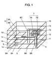
- Fig. 1 is a vision-through perspective view of a module using a low-temperature fired ceramic (hereinafter referred to as "LTCC") substrate that is employed as the electronic component.
- Fig. 1 illustrates a module employing four dielectric substrates 1a, 1b, 1c and 1d, for example.
- Conductive metal patterns made of copper or silver are formed between dielectric substrates 1a and 1b, between dielectric substrates 1b and 1c, and between dielectric substrates 1c and 1d.
- the number of dielectric substrates 1a through 1d is four, for example, five pattern forming layers 11, 12, 13, 14 and 15 defining a pattern can be formed.
- External terminal 3 for input is connected to capacitor unit region 6 having capacitor electrode units 6A and 6B through wiring pattern 9A and via hole 8A, and then connected to branched wiring pattern 9B.
- One side of branched wiring pattern 9B is connected to external terminal 4 for output through via hole 8B.
- the other side of branched wiring pattern 9B is connected to inductor unit region 7, and then connected to external terminal 5 for installation through via hole 8C.
- Fig. 2 is an expanded plan view of pattern forming layers 11, 12, 13, 14 and 15 of Fig. 1. Same elements used in Fig. 1 are denoted with the same reference marks.
- Pattern forming layers 11 has a pattern for the external terminal that is to be electrically connected to a terminal existing on a printed board mainly when the module is mounted to the printed board.
- Capacitor unit region 6 is formed of rectangular pattern 6B of pattern forming layer 12 and rectangular pattern 6A of pattern forming layer 13. In other words, rectangular patterns 6A and 6B are formed as electrode units of capacitor unit region 6.
- Inductor unit 7 is formed of spiral pattern 7B of pattern forming layer 13 and spiral pattern 7A of pattern forming layer 14. No pattern is formed in outermost pattern forming layer 15.
- a pattern for connection for allowing electric connection to the chip-shaped electronic component may be formed in pattern forming layer 15.
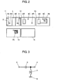
- Fig. 3 shows an electrically equivalent circuit formed based on the wiring information of Fig. 1 and Fig. 2.
- the configuration of the electric circuit of Fig. 3 has an electric circuit function as a high pass filer (so-called HPF).
- HPF high pass filer
- the high pass filer passes only power that has frequencies higher than a specific frequency, of power fed from external terminal 3 for input, to external terminal 4 for output.
- Fig. 4 is a flowchart used for designing the module employing such an LTCC substrate.
- a predetermined electrical characteristic as a target is firstly determined in step 21.
- the predetermined electrical characteristic may be a band width of a high-frequency filter or a cut-off frequency, for example.
- an electric constant of the module is determined by a first electric circuit simulation incorporated in CAD system 40.
- step 23 for achieving the electrical characteristic determined in step 22, thickness of the LTCC substrate and a pattern shape of the conductive metal are determined.
- step 24 layout design is performed.
- the pattern formation and the layout design are performed using a mechanical three-dimensional CAD, the designing efficiency of a multilayer circuit component formed by integrating electronic component regions in a three-dimensional space can be increased.
- the multilayer circuit component is a module using the LTCC substrate, for example.
- step 25 a second electric circuit simulation is performed in consideration of the number of via holes 8A, 8B and 8C and the length of wiring patterns 9A and 9B (Fig. 1).
- the second electric circuit simulation is also incorporated in CAD system 40.
- the result of the second electric circuit simulation does not match with a target electrical characteristic or largely separates from a predetermined range (characteristic NG1), for reducing these errors, the shape of the conductive metal pattern, the position of the electronic component region in the module, and the lengths and positions of the via holes and the wiring patterns are varied. For varying them, the process returns to step 23, and the processes of step 23 and later are performed.
- step 26 the electrical characteristic of an actually produced module is measured, and it is determined whether or not this electrical characteristic matches with the target electrical characteristic.
- the predetermined electrical characteristic is obtained in step 26 (characteristic OK2)
- the design of the electronic component is completed.
- the processes of step 23 and later are performed again.
- Electromagnetic coupling is apt to occur in the electronic component region such as capacitor unit region 6 or inductor unit region 7, between via holes 8A, 8B and 8C, and between wiring patterns 9A and 9B.
- an electromagnetic field simulator for solving a Maxwell equation based on the module configuration and electric boundary condition is used.
- the electromagnetic analysis problems occur that more electronic components are generally required and the calculation time sharply increases with increase in circuit scale, though the occurrence depends on the method of the analysis. Therefore, when the electromagnetic analysis is incorporated into the designing procedure of the whole module, sufficient designing efficiency cannot be obtained.
- the method of the present invention where the electromagnetic analysis is applied to only a single electronic component region having a certain three-dimensional shape does not take much time.
- the single electronic component region is capacitor unit region 6 or inductor unit region 7, for example. Therefore, the electrical characteristic corresponding to the electronic component region can be relatively easily obtained.
- the electrical characteristics of capacitor unit region 6 and inductor unit region 7 are not calculated as concentrated constants of the capacity and inductance itself, but are calculated using the electrical characteristic that is obtained by electromagnetically analyzing the single electronic component region having the three-dimensional shape.
- the electrical characteristic can be simulated in consideration of effects of various parasitic components such as parasitic inductor and parasitic capacity of capacitor unit region 6 and inductor unit region 7, and accurate prediction of the electrical characteristic is allowed.
- the result of the electromagnetic analysis of the certain single electronic component region can be stored as the three-dimensional shape information of the electronic component and a pair of electrical characteristic data corresponding to it.
- the three-dimensional shape information of the electronic component and electrical characteristic data corresponding to it can be produced.
- the efficiency of the pattern shape determining procedure of step 23 is largely increased.
- the efficiency of the layout designing procedure in step 24 can be largely increased by the following processes:
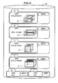
- Fig. 5 is a schematic diagram of a database for storing, as a pair of data, three-dimensional shape information 3DI of electronic components A through F and electrical characteristics of the electronic components that is obtained by electromagnetic analysis based on three-dimensional shape information 3DI.
- Fig. 5 shows database 50.
- Three-dimensional shape information 3DI and various electrical characteristics of each electronic component shown below are stored in database 50, for example.
- Electronic component A shown in the first stage from the top in Fig. 5 is a capacitor, for example.
- Three-dimensional shape information 3DI of the capacitor is shown using width (W), length (L), and height (H). They are 0.8 mm, 0.8 mm, and 0.4 mm.
- the size of an electrode is 0.6 mm ⁇ 0.6 mm.
- Electric characteristic 5EA of electronic component A is the characteristic of impedance ZA for frequency (f), for example, and is stored in database 50.
- Electronic component B shown in the second stage from the top in Fig. 5 is a capacitor similarly to electronic component A.
- Three-dimensional shape information 3DI of the capacitor of electronic component B is shown using width (W), length (L), and height (H). They are 1.4 mm, 1.2 mm, and 0.2 mm.
- the size of an electrode is 1.0 mm ⁇ 0.8 mm.
- Electric characteristic 5EB of electronic component B is the characteristic of impedance ZB for frequency (f).
- Electronic component B is selected so that its capacity is larger than that of the capacitor of electronic component A, for example. Impedance ZB of electronic component B is therefore smaller than that of electronic component A.
- Electronic component C shown in the third stage from the top in Fig. 5 is an inductor.
- Width (W), length (L), and height (H) of electronic component C are 1.0 mm, 1.0 mm, and 0.6 mm.
- a spiral inductor is formed on the outermost surface.
- Electric characteristic 5EC of electronic component C is the characteristic of impedance ZC for frequency (f), for example, similarly to electronic components A and B.
- Electronic component D shown in the fourth stage from the top in Fig. 5 is an inductor similarly to electronic component C.
- Width (W), length (L), and height (H) of electronic component D are 1.5 mm, 0.8 mm, and 0.6 mm.
- a spiral inductor is formed on the outermost surface.
- Electric characteristic 5ED of electronic component C is the characteristic of impedance ZD for frequency (f), for example, similarly to electronic components A, B and C, and its size is stored in database 50.
- Electronic component D is selected so that its inductance is larger than that of the inductor of electronic component C, for example. Impedance of electronic component D is therefore larger than that of electronic component C.
- Fig. 5 shows electrical characteristics 5EE and 5EF as three-dimensional shape information 3DI of electronic components E and F extremely schematically for convenience sake.
- Electronic components E and F may be capacitors, inductors, or the other electronic components such as resistors.
- Fig. 6 is a schematic diagram of the database additionally having an allowance clearance as an attribute in accordance with the exemplary embodiment.
- the allowance clearance that determines layout interval between each electronic component and another electronic component adjacent to it when the various electronic components are laid out on the LTCC substrate, for example, is stored as the three-dimensional shape information.
- electromagnetic analysis is performed based on three-dimensional shape information 3DI of each of electronic components A through F, and the interval between each electronic component and the adjacent electronic component at which the electric field strength is sufficiently small around the electronic components is determined as allowance clearance ACL, and is stored in the database.
- allowance clearances ACL, BCL, CCL and DCL of electronic components A, B, C and D are 0.05 mm, 0.1 mm, 0.15 mm and 0.05 mm, respectively. Allowance clearances ACL through DCL can be defined as interval S (shown by broken lines) between each of electronic components A through D and its adjacent electronic component (not shown) in Fig. 6. Interval S therefore corresponds to each allowance clearance. Allowance clearances as three-dimensional shape information 3DI of electronic components E and F are not shown for convenience sake.
- Fig. 6 schematically shows electrical characteristics 6EA, 6EB, 6EC, 6ED, 6EE and 6EF of electronic components A through F. These electrical characteristics may be impedance of electronic components as shown in Fig. 5, or may be other electrical characteristic such as a capacitance characteristic or an inductance characteristic.
- step 21 of Fig. 4 a target electrical characteristic is set.
- step 22 of step 22 electric constants C and L of capacitor unit region 6 and inductor unit region 7 (Fig. 1) are determined using the first electric circuit simulator incorporated in CAD system 40.
- step 23 a pattern shape for obtaining electric constants C and L and thickness of electronic component regions such as capacitor unit region 6 and inductor unit region 7 are determined.
- determining three-dimensional shape information 3DI of such electronic components an electronic component that has the electric constant closest to the electric constant such as C or L determined in step 22 is retrieved from database 50 shown in Fig. 5, and appropriate electronic components are selected.
- step 24 layout design of laying out and directing the selected electronic components in the three-dimensional space in a module is performed.
- a two-dimensional CAD or a printed board for creating a plan view is not useful.
- a three-dimensional CAD capable of effectively making effective use of the data is useful for layout design.
- a conventional layout design is performed based on designers' past experience, under various constraints that electromagnetic coupling is prevented between the electronic components and the volume of the module is minimized.
- the layout design can be performed while the electromagnetic coupling between the electronic components is minimized, so that the designing efficiency can be increased.
- the electronic components are electrically interconnected through via holes 8A, 8B and 8C and wiring patterns 9A and 9B (Fig. 1) based on the wiring information of the electrically equivalent circuits shown in Fig. 3.
- three-dimensional shape information 3DI responsive to via holes 8A, 8B and 8C and wiring patterns 9A and 9B, and electrical characteristics 6EA through 6EF corresponding to it, as well as the other electronic component region, are stored in database 60 shown in Fig. 6..
- the layout design can be advantageously performed while minimizing not only the electromagnetic coupling between the electronic components but also the electromagnetic coupling between the electronic component region, such as capacitor unit region 6 or inductor unit region 7, and via holes 8A, 8B and 8C or between the electronic component region and wiring patterns 9A and 9B.
- three-dimensional shape information 3DI such as electrical characteristics 5EA through 5EF (6EA through 6EF) of used electronic components A through F, the number of via holes 8A, 8B and 8C, and the length of wiring patterns 9A and 9B is determined. Therefore, the second electric circuit simulation considering them can be performed in step 25.
- the second electric circuit simulation is incorporated in CAD system 40.
- step 26 the electrical characteristic of the actually produced module is measured, and it is determined whether it matches with the predetermined electrical characteristic as the target.
- the second electric circuit simulation considering three-dimensional shape information 3DI can be performed in step 25 (Fig. 4). Therefore, an accurate electrical characteristic can be obtained, simulation does not need to be repeated many times, and hence the designing efficiency can be increased. Adding the electric circuit simulation function to CAD system 40 allows repetition of these procedures in the same system and hence increases the designing efficiency.
- step 24 when step 24 is performed using database 60 of Fig. 6, simulation does not need to be repeated many times, the design can be performed always considering the electromagnetic coupling, and hence the designing efficiency is increased
- the present embodiment has been described using an LTCC substrate as the substrate material, an HPF as the circuit, and frequency and impedance as the electrical characteristics.
- another dielectric material may be used as the substrate material, and another characteristic such as a band pass filter may be used as the electrical characteristic.
- a designing method of an electronic component of the present invention has an advantage of increasing the designing efficiency, and is useful especially in a CAD system for designing a multilayer circuit component. Its industrial applicability is therefore high.
Abstract
A designing method of an electronic component aiming at increase in designing efficiency is provided. The designing method has step (21) of setting a predetermined electrical characteristic, step (22) of determining an electric constant of the component with a first electric circuit simulation to satisfy the predetermined electrical characteristic, step (23) of determining a pattern shape for obtaining the electric constant, step (24) of retrieving and selecting an electronic component matching with the electric constant from a database, and performing layout design using the selected electronic component as a module, step (25) of performing a second electric circuit simulation, and step (26) of determining whether the electrical characteristic of the module matches with the predetermined electrical characteristic.
Description
- The present invention relates to a designing method of an electronic component.
- Fig. 7 shows a designing method of an electronic component, especially a flowchart using a CAD (computer-aided design) system. In starting the design of the electronic component, a predetermined electrical characteristic is determined in
step 101. Instep 102, electric constants of electrically equivalent circuits and the electronic components constituting them are determined by an electric circuit simulator or the like so that the electrical characteristic determined instep 101 satisfies a predetermined value. Instep 103, physical shapes and conductive metal patterns of the electronic components or the like for achieving the electric constants determined instep 102 are determined. - Then, in
step 104, based on the physical shapes of various electronic components determined instep 102, the electronic components or the like are laid out in a module, and wiring patterns between the electronic components and external terminals or the like are formed. Instep 105, an electrical characteristic is measured, and it is determined whether or not electrical characteristic matches with the predetermined electrical characteristic determined instep 101. When the predetermined electrical characteristic is not achieved, the process returns tostep 103, and the processes ofstep 103 and later are repeated. When the predetermined electrical characteristic is achieved instep 105, all processes are completed. - In the conventional example, however, the designing efficiency is low.
- In the conventional configuration, the determination of the pattern shape of
step 103 and layout design ofstep 104 have not been yet completed at the time of the electric circuit simulation ofstep 102, so that the electric circuit simulation considering the layout cannot be performed. Therefore, in the measurement stage of the electrical characteristic ofstep 105, frequently, the measured electrical characteristic does not match with the predetermined electrical characteristic. The simulation must be therefore repeated many times, and hence it is not easy to increase the designing efficiency. The electric circuit simulation ofstep 102 is performed by the electric circuit simulator, and the other steps are performed by a CAD system, so that the designing efficiency is not increased against expectations. - Conventional arts related to the present invention are disclosed in
Japanese Patent Unexamined Publication No. 2003-16133 Japanese Patent Unexamined Publication No. 2002-73718 - The present invention provides a designing method of an electronic component where the designing efficiency is increased. The designing method of the present invention additionally has a function of performing electric circuit simulation, and a step of performing the electric circuit simulation is added between the designing step of the layout and the measuring step of the electrical characteristic.
- An electric circuit simulation considering the layout can be performed in this method, so that the problem that the simulation must be performed again can be solved. Since the electric circuit simulation is used as a function in the system, processing between systems can be avoided and the designing efficiency can be increased.
- A specific designing method of an electronic component of the present invention has the following steps:
- a first step of setting a predetermined electrical characteristic;
- a second step of determining an electric constant of the electronic component with a first electric circuit simulation to satisfy the electrical characteristic;
- a third step of determining a physical pattern shape to obtain the electric constant of the electronic component;
- a fourth step of retrieving and selecting an electronic component having a predetermined electric constant from a database, and performing layout design using the selected electronic component as a module;
- a fifth step of performing a second electric circuit simulation after the fourth step of performing the layout design; and
- a sixth step of measuring the electrical characteristic of the module, and determining whether the measured electrical characteristic matches with the predetermined electrical characteristic.
- In the designing method of the electronic component of the present invention, the three-dimensional shape information and electrical characteristic of the electronic component are stored in the database.
- In the designing method of the electronic component of the present invention, the three-dimensional information of an allowance clearance is stored in the database. Here, the allowance clearance defines the layout interval between the electronic component and another electronic component that is adjacent to it when the electronic components are laid out.
- In the designing method of the electronic component of the present invention, the three-dimensional shape information about a wiring pattern and a via hole that connect the electronic component to other electronic components is stored in the database.
- In the designing method of the electronic component of the present invention, the processes of the third step and later are performed after the fifth step.
- In the designing method of the electronic component of the present invention, the processes of the third step and later are performed after the sixth step.
- In the designing method of the electronic component of the present invention, the processes of the second, third, fourth, and fifth steps are performed by the same CAD system.
- In the designing method of the electronic component of the present invention, the electronic component is formed on a low-temperature fired ceramic substrate.
- In the designing method of the electronic component of the present invention, the electronic component includes at least one of a capacitor, an inductor, and a resistor.
- In the designing method of the electronic component of the present invention, the low-temperature fired ceramic substrate is a multilayer circuit board.
-
- Fig. 1 is a vision-through perspective view of a multilayer circuit component module in accordance with an exemplary embodiment of the present invention.
- Fig. 2 is an expanded plan view of pattern forming layers in accordance with the exemplary embodiment.
- Fig. 3 is an electrically equivalent circuit diagram of the multilayer circuit component module in accordance with the exemplary embodiment.
- Fig. 4 is a flowchart showing a module designing procedure in accordance with the exemplary embodiment.
- Fig. 5 is a schematic diagram of a form of a database in accordance with the exemplary embodiment.
- Fig. 6 is a schematic diagram of the database additionally having an allowance clearance as an attribute in accordance with the exemplary embodiment.
- Fig. 7 is a flowchart showing a conventional module designing procedure.
-
- 1 dielectric substrate
- 3 external terminal for input
- 4 external terminal for output
- 5 external terminal for installation
- 6 capacitor unit region
- 6A, 6B rectangular patterns
- 7 inductor unit region
- 7A, 7B spiral patterns
- 8A, 8B, 8C via holes
- 9A, 9B wiring patterns
- 11, 12, 13, 14, 15 pattern forming layers
- A designing method of the electronic component using a CAD system in accordance with an exemplary embodiment of the present invention will be described hereinafter with reference to the drawings.
- Fig. 1 is a vision-through perspective view of a module using a low-temperature fired ceramic (hereinafter referred to as "LTCC") substrate that is employed as the electronic component. Fig. 1 illustrates a module employing four
dielectric substrates dielectric substrates dielectric substrates dielectric substrates dielectric substrates 1a through 1d is four, for example, fivepattern forming layers -
External terminal 3 for input is connected tocapacitor unit region 6 havingcapacitor electrode units wiring pattern 9A and viahole 8A, and then connected to branchedwiring pattern 9B. One side of branchedwiring pattern 9B is connected toexternal terminal 4 for output through viahole 8B. The other side of branchedwiring pattern 9B is connected toinductor unit region 7, and then connected toexternal terminal 5 for installation through viahole 8C. - Fig. 2 is an expanded plan view of
pattern forming layers Pattern forming layers 11 has a pattern for the external terminal that is to be electrically connected to a terminal existing on a printed board mainly when the module is mounted to the printed board.Capacitor unit region 6 is formed ofrectangular pattern 6B ofpattern forming layer 12 andrectangular pattern 6A ofpattern forming layer 13. In other words,rectangular patterns capacitor unit region 6. -
Inductor unit 7 is formed ofspiral pattern 7B ofpattern forming layer 13 andspiral pattern 7A ofpattern forming layer 14. No pattern is formed in outermostpattern forming layer 15. When a chip-shaped electronic component (not shown) is further mounted to the surface of the module, a pattern for connection for allowing electric connection to the chip-shaped electronic component may be formed inpattern forming layer 15. - Fig. 3 shows an electrically equivalent circuit formed based on the wiring information of Fig. 1 and Fig. 2. The configuration of the electric circuit of Fig. 3 has an electric circuit function as a high pass filer (so-called HPF). The high pass filer passes only power that has frequencies higher than a specific frequency, of power fed from
external terminal 3 for input, toexternal terminal 4 for output. - Fig. 4 is a flowchart used for designing the module employing such an LTCC substrate. In starting to design an electronic component, a predetermined electrical characteristic as a target is firstly determined in
step 21. Here, the predetermined electrical characteristic may be a band width of a high-frequency filter or a cut-off frequency, for example. Instep 22, for achieving the predetermined electrical characteristic, an electric constant of the module is determined by a first electric circuit simulation incorporated inCAD system 40. Instep 23, for achieving the electrical characteristic determined instep 22, thickness of the LTCC substrate and a pattern shape of the conductive metal are determined. - Then, in
step 24, layout design is performed. When the pattern formation and the layout design are performed using a mechanical three-dimensional CAD, the designing efficiency of a multilayer circuit component formed by integrating electronic component regions in a three-dimensional space can be increased. Here, the multilayer circuit component is a module using the LTCC substrate, for example. - In
step 25, a second electric circuit simulation is performed in consideration of the number of viaholes wiring patterns CAD system 40. When the result of the second electric circuit simulation (step 25) does not match with a target electrical characteristic or largely separates from a predetermined range (characteristic NG1), for reducing these errors, the shape of the conductive metal pattern, the position of the electronic component region in the module, and the lengths and positions of the via holes and the wiring patterns are varied. For varying them, the process returns to step 23, and the processes ofstep 23 and later are performed. When the result of the second electric circuit simulation substantially matches with the predetermined electrical characteristic and is allowable in design (characteristic OK1), the process goes to step 26. Instep 26, the electrical characteristic of an actually produced module is measured, and it is determined whether or not this electrical characteristic matches with the target electrical characteristic. When the predetermined electrical characteristic is obtained in step 26 (characteristic OK2), the design of the electronic component is completed. When the measured electrical characteristic is out of the predetermined allowance range, the processes ofstep 23 and later are performed again. - When the frequency band where the module employing the LTCC substrate is used is in a high frequency region, various parasitic components are apt to be added to
capacitor unit region 6 orinductor unit region 7. Electromagnetic coupling is apt to occur in the electronic component region such ascapacitor unit region 6 orinductor unit region 7, between viaholes wiring patterns - In the electromagnetic analysis, problems occur that more electronic components are generally required and the calculation time sharply increases with increase in circuit scale, though the occurrence depends on the method of the analysis. Therefore, when the electromagnetic analysis is incorporated into the designing procedure of the whole module, sufficient designing efficiency cannot be obtained. However, the method of the present invention where the electromagnetic analysis is applied to only a single electronic component region having a certain three-dimensional shape does not take much time. Here, the single electronic component region is
capacitor unit region 6 orinductor unit region 7, for example. Therefore, the electrical characteristic corresponding to the electronic component region can be relatively easily obtained. - In the second electric circuit simulation of
step 25, the electrical characteristics ofcapacitor unit region 6 andinductor unit region 7 are not calculated as concentrated constants of the capacity and inductance itself, but are calculated using the electrical characteristic that is obtained by electromagnetically analyzing the single electronic component region having the three-dimensional shape. Thus, the electrical characteristic can be simulated in consideration of effects of various parasitic components such as parasitic inductor and parasitic capacity ofcapacitor unit region 6 andinductor unit region 7, and accurate prediction of the electrical characteristic is allowed. - The result of the electromagnetic analysis of the certain single electronic component region can be stored as the three-dimensional shape information of the electronic component and a pair of electrical characteristic data corresponding to it. When such simulation is performed in various electronic component regions, the three-dimensional shape information of the electronic component and electrical characteristic data corresponding to it can be produced. In the stage of the first electric circuit simulation of
step 22, it has not been determined which pattern shape of electronic component region is used. However, when the pattern shape is determined instep 22, and the three-dimensional shape information of the electronic component region that has the electrical characteristic closest to the predetermined electrical characteristic is automatically extracted from the database, the efficiency of the pattern shape determining procedure ofstep 23 is largely increased. Further, the efficiency of the layout designing procedure instep 24 can be largely increased by the following processes: - automatically extracting, from the database, the three-dimensional shape information of the electronic component region that has the electrical characteristic closest to the electrical characteristic required for layout design in
step 24 ; and - automatically laying out the information in a three-dimensional space in the module under various constraints such as minimizing the volume of the module or minimizing the whole length of
wiring patterns - A specific embodiment of the present invention is described hereinafter with reference to Fig. 5 and Fig. 6. Fig. 5 is a schematic diagram of a database for storing, as a pair of data, three-dimensional shape information 3DI of electronic components A through F and electrical characteristics of the electronic components that is obtained by electromagnetic analysis based on three-dimensional shape information 3DI.
- Fig. 5 shows
database 50. Three-dimensional shape information 3DI and various electrical characteristics of each electronic component shown below are stored indatabase 50, for example. Electronic component A shown in the first stage from the top in Fig. 5 is a capacitor, for example. Three-dimensional shape information 3DI of the capacitor is shown using width (W), length (L), and height (H). They are 0.8 mm, 0.8 mm, and 0.4 mm. The size of an electrode is 0.6 mm × 0.6 mm. Electric characteristic 5EA of electronic component A is the characteristic of impedance ZA for frequency (f), for example, and is stored indatabase 50. - Electronic component B shown in the second stage from the top in Fig. 5 is a capacitor similarly to electronic component A. Three-dimensional shape information 3DI of the capacitor of electronic component B is shown using width (W), length (L), and height (H). They are 1.4 mm, 1.2 mm, and 0.2 mm. The size of an electrode is 1.0 mm × 0.8 mm. Electric characteristic 5EB of electronic component B is the characteristic of impedance ZB for frequency (f). Electronic component B is selected so that its capacity is larger than that of the capacitor of electronic component A, for example. Impedance ZB of electronic component B is therefore smaller than that of electronic component A.
- Electronic component C shown in the third stage from the top in Fig. 5 is an inductor. Width (W), length (L), and height (H) of electronic component C are 1.0 mm, 1.0 mm, and 0.6 mm. A spiral inductor is formed on the outermost surface. Electric characteristic 5EC of electronic component C is the characteristic of impedance ZC for frequency (f), for example, similarly to electronic components A and B.
- Electronic component D shown in the fourth stage from the top in Fig. 5 is an inductor similarly to electronic component C. Width (W), length (L), and height (H) of electronic component D are 1.5 mm, 0.8 mm, and 0.6 mm. A spiral inductor is formed on the outermost surface. Electric characteristic 5ED of electronic component C is the characteristic of impedance ZD for frequency (f), for example, similarly to electronic components A, B and C, and its size is stored in
database 50. - Electronic component D is selected so that its inductance is larger than that of the inductor of electronic component C, for example. Impedance of electronic component D is therefore larger than that of electronic component C.
- The lowest stage in Fig. 5 shows electrical characteristics 5EE and 5EF as three-dimensional shape information 3DI of electronic components E and F extremely schematically for convenience sake. Electronic components E and F may be capacitors, inductors, or the other electronic components such as resistors.
- Fig. 6 is a schematic diagram of the database additionally having an allowance clearance as an attribute in accordance with the exemplary embodiment. In Fig. 6, the allowance clearance that determines layout interval between each electronic component and another electronic component adjacent to it when the various electronic components are laid out on the LTCC substrate, for example, is stored as the three-dimensional shape information.
- Specifically, electromagnetic analysis is performed based on three-dimensional shape information 3DI of each of electronic components A through F, and the interval between each electronic component and the adjacent electronic component at which the electric field strength is sufficiently small around the electronic components is determined as allowance clearance ACL, and is stored in the database.
- In Fig. 6, allowance clearances ACL, BCL, CCL and DCL of electronic components A, B, C and D are 0.05 mm, 0.1 mm, 0.15 mm and 0.05 mm, respectively. Allowance clearances ACL through DCL can be defined as interval S (shown by broken lines) between each of electronic components A through D and its adjacent electronic component (not shown) in Fig. 6. Interval S therefore corresponds to each allowance clearance. Allowance clearances as three-dimensional shape information 3DI of electronic components E and F are not shown for convenience sake.
- Fig. 6 schematically shows electrical characteristics 6EA, 6EB, 6EC, 6ED, 6EE and 6EF of electronic components A through F. These electrical characteristics may be impedance of electronic components as shown in Fig. 5, or may be other electrical characteristic such as a capacitance characteristic or an inductance characteristic.
- A designing method of an electronic component of the present invention is described hereinafter with reference to Fig. 1 through Fig. 6. First, in
step 21 of Fig. 4, a target electrical characteristic is set. Then, instep 22, for achieving this electrical characteristic, electric constants C and L ofcapacitor unit region 6 and inductor unit region 7 (Fig. 1) are determined using the first electric circuit simulator incorporated inCAD system 40. - Then, in
step 23, a pattern shape for obtaining electric constants C and L and thickness of electronic component regions such ascapacitor unit region 6 andinductor unit region 7 are determined. In determining three-dimensional shape information 3DI of such electronic components, an electronic component that has the electric constant closest to the electric constant such as C or L determined instep 22 is retrieved fromdatabase 50 shown in Fig. 5, and appropriate electronic components are selected. - Then, in
step 24, layout design of laying out and directing the selected electronic components in the three-dimensional space in a module is performed. For laying out and directing the electronic components in the three-dimensional space, a two-dimensional CAD or a printed board for creating a plan view is not useful. When the three-dimensional shape information data used in the previously performed three-dimensional electric analysis is prepared for each electronic component, a three-dimensional CAD capable of effectively making effective use of the data is useful for layout design. A conventional layout design is performed based on designers' past experience, under various constraints that electromagnetic coupling is prevented between the electronic components and the volume of the module is minimized. - When
database 60 shown in Fig. 6 is used, however, the layout design can be performed while the electromagnetic coupling between the electronic components is minimized, so that the designing efficiency can be increased. After the layout design of the electronic components, the electronic components are electrically interconnected through viaholes wiring patterns holes wiring patterns database 60 shown in Fig. 6.. Thus, the layout design can be advantageously performed while minimizing not only the electromagnetic coupling between the electronic components but also the electromagnetic coupling between the electronic component region, such ascapacitor unit region 6 orinductor unit region 7, and viaholes wiring patterns - In the procedure discussed above, three-dimensional shape information 3DI such as electrical characteristics 5EA through 5EF (6EA through 6EF) of used electronic components A through F, the number of via
holes wiring patterns step 25. The second electric circuit simulation is incorporated inCAD system 40. - Finally, in
step 26, the electrical characteristic of the actually produced module is measured, and it is determined whether it matches with the predetermined electrical characteristic as the target. - In this designing method of the present invention, the second electric circuit simulation considering three-dimensional shape information 3DI can be performed in step 25 (Fig. 4). Therefore, an accurate electrical characteristic can be obtained, simulation does not need to be repeated many times, and hence the designing efficiency can be increased. Adding the electric circuit simulation function to
CAD system 40 allows repetition of these procedures in the same system and hence increases the designing efficiency. - Further, when
step 24 is performed usingdatabase 60 of Fig. 6, simulation does not need to be repeated many times, the design can be performed always considering the electromagnetic coupling, and hence the designing efficiency is increased - The present embodiment has been described using an LTCC substrate as the substrate material, an HPF as the circuit, and frequency and impedance as the electrical characteristics. However, another dielectric material may be used as the substrate material, and another characteristic such as a band pass filter may be used as the electrical characteristic.
- A designing method of an electronic component of the present invention has an advantage of increasing the designing efficiency, and is useful especially in a CAD system for designing a multilayer circuit component. Its industrial applicability is therefore high.
Claims (10)
- A designing method of an electronic component comprising:a first step of setting a predetermined electrical characteristic of the electronic component;a second step of determining an electric constant of the electronic component with a first electric circuit simulation so as to satisfy the electrical characteristic;a third step of determining a pattern shape for obtaining the electric constant;a fourth step of retrieving and selecting an electronic component matching with the electric constant from a database, and performing layout design using the selected electronic component as a module;a fifth step of performing a second electric circuit simulation after the fourth step of performing the layout design; anda sixth step of determining whether an electrical characteristic of the module matches with the predetermined electrical characteristic.
- The designing method of the electronic component of claim 1, wherein,
three-dimensional shape information of the electronic component and an electrical characteristic of the electronic component are stored in the database. - The designing method of the electronic component of claim 1, wherein,
three-dimensional information of an allowance clearance is stored in the database, the allowance clearance defining a layout interval between the electronic component and another electronic component that is adjacent to the electronic component when the electronic component is laid out. - The designing method of the electronic component of claim 2 or claim 3, wherein,
three-dimensional shape information of a wiring pattern and a via hole that couple the electronic component to another electronic component is stored in the database. - The designing method of the electronic component of claim 1, wherein,
processes of the third step and later are performed after a process of the fifth step is performed. - The designing method of the electronic component of claim 1, wherein,
processes of the third step and later are performed after a process of the sixth step is performed. - The designing method of the electronic component of claim 1, wherein,
processes of the second, third, fourth, and fifth steps are performed by the same CAD system. - The designing method of the electronic component of claim 1, wherein,
the electronic component is formed on a low-temperature fired ceramic substrate. - The designing method of the electronic component of claim 8, wherein,
the electronic component includes at least one of a capacitor, an inductor, and a resistor. - The designing method of the electronic component of claim 8, wherein,
the low-temperature fired ceramic substrate is a multilayer circuit board.
Applications Claiming Priority (2)
| Application Number | Priority Date | Filing Date | Title |
|---|---|---|---|
| JP2005114144A JP2006293726A (en) | 2005-04-12 | 2005-04-12 | Design method of electronic component |
| PCT/JP2006/307612 WO2006109785A1 (en) | 2005-04-12 | 2006-04-11 | Method for designing electronic component |
Publications (2)
| Publication Number | Publication Date |
|---|---|
| EP1791069A1 true EP1791069A1 (en) | 2007-05-30 |
| EP1791069A4 EP1791069A4 (en) | 2010-11-10 |
Family
ID=37087056
Family Applications (1)
| Application Number | Title | Priority Date | Filing Date |
|---|---|---|---|
| EP06731559A Withdrawn EP1791069A4 (en) | 2005-04-12 | 2006-04-11 | Method for designing electronic component |
Country Status (5)
| Country | Link |
|---|---|
| US (1) | US7496875B2 (en) |
| EP (1) | EP1791069A4 (en) |
| JP (1) | JP2006293726A (en) |
| CN (1) | CN101010675A (en) |
| WO (1) | WO2006109785A1 (en) |
Cited By (1)
| Publication number | Priority date | Publication date | Assignee | Title |
|---|---|---|---|---|
| EP2079290A3 (en) * | 2008-01-11 | 2010-03-17 | Northrop Grumman Systems Corporation | Multilayer passive circuit topology |
Families Citing this family (7)
| Publication number | Priority date | Publication date | Assignee | Title |
|---|---|---|---|---|
| JP2008293066A (en) * | 2007-05-22 | 2008-12-04 | Panasonic Corp | Library for electronic circuit simulation, library generating system, recording medium storing them, and method for manufacturing electronic apparatus using them |
| JP4856269B1 (en) * | 2010-09-06 | 2012-01-18 | 株式会社東芝 | Wiring design support apparatus and wiring design support method |
| US8775998B2 (en) * | 2010-12-09 | 2014-07-08 | Panasonic Corporation | Support device of three-dimensional integrated circuit and method thereof |
| CN103678814B (en) * | 2013-12-18 | 2016-06-29 | 北京航空航天大学 | The eccentricity prebias method for designing of critical inclination near-circular orbit |
| CN103853887B (en) * | 2014-03-05 | 2016-09-14 | 北京航空航天大学 | The satellite orbit of the eccentricity of a kind of Frozen Orbit determines method |
| CN108629103B (en) * | 2015-04-08 | 2022-02-11 | 上海望友信息科技有限公司 | SMT patch manufacturing and SMT screen plate manufacturing method and system |
| US10244873B2 (en) | 2015-10-01 | 2019-04-02 | Isee Store Innovations, Llc | Adjustable product display system and method |
Citations (4)
| Publication number | Priority date | Publication date | Assignee | Title |
|---|---|---|---|---|
| US5689600A (en) * | 1995-01-20 | 1997-11-18 | Minnesota Mining And Manufacturing Company | Electronic circuit structure |
| US6021050A (en) * | 1998-12-02 | 2000-02-01 | Bourns, Inc. | Printed circuit boards with integrated passive components and method for making same |
| US20030001839A1 (en) * | 2000-01-21 | 2003-01-02 | Tatsuhiro Matsuda | System for generating printed board three-dimensional shape data |
| JP2003216680A (en) * | 2002-01-17 | 2003-07-31 | Fujitsu Ltd | Clearance check method in cad for printed circuit board and computer program |
Family Cites Families (9)
| Publication number | Priority date | Publication date | Assignee | Title |
|---|---|---|---|---|
| US5544067A (en) * | 1990-04-06 | 1996-08-06 | Lsi Logic Corporation | Method and system for creating, deriving and validating structural description of electronic system from higher level, behavior-oriented description, including interactive schematic design and simulation |
| JP2898493B2 (en) * | 1992-11-26 | 1999-06-02 | 三菱電機株式会社 | Layout design method and layout design apparatus for millimeter-wave or microwave IC |
| JPH09204451A (en) * | 1996-01-24 | 1997-08-05 | Sony Corp | Board designing device |
| JPH1166122A (en) * | 1997-08-13 | 1999-03-09 | Fujitsu Ltd | Analytic model generating method and storage medium where program thereof is stored |
| JP2002073718A (en) * | 2000-09-04 | 2002-03-12 | Tdk Corp | Design system, designing method and manufacturing method for high-frequency electronic component |
| US6665854B2 (en) * | 2000-12-04 | 2003-12-16 | Matsushita Electric Industrial Co., Ltd. | Method and apparatus of checking mount quality of circuit board |
| JP2003016133A (en) | 2001-04-27 | 2003-01-17 | Tdk Corp | High-frequency electronic component and its designing method |
| JP2005026312A (en) | 2003-06-30 | 2005-01-27 | Hitachi Metals Ltd | High-frequency electronic part and its mounting method |
| US20060265677A1 (en) * | 2005-05-20 | 2006-11-23 | Cadence Design Systems, Inc. | Method and system for increased accuracy for extraction of electrical parameters |
-
2005
- 2005-04-12 JP JP2005114144A patent/JP2006293726A/en active Pending
-
2006
- 2006-04-11 US US11/629,909 patent/US7496875B2/en not_active Expired - Fee Related
- 2006-04-11 EP EP06731559A patent/EP1791069A4/en not_active Withdrawn
- 2006-04-11 CN CNA2006800006961A patent/CN101010675A/en active Pending
- 2006-04-11 WO PCT/JP2006/307612 patent/WO2006109785A1/en active Application Filing
Patent Citations (4)
| Publication number | Priority date | Publication date | Assignee | Title |
|---|---|---|---|---|
| US5689600A (en) * | 1995-01-20 | 1997-11-18 | Minnesota Mining And Manufacturing Company | Electronic circuit structure |
| US6021050A (en) * | 1998-12-02 | 2000-02-01 | Bourns, Inc. | Printed circuit boards with integrated passive components and method for making same |
| US20030001839A1 (en) * | 2000-01-21 | 2003-01-02 | Tatsuhiro Matsuda | System for generating printed board three-dimensional shape data |
| JP2003216680A (en) * | 2002-01-17 | 2003-07-31 | Fujitsu Ltd | Clearance check method in cad for printed circuit board and computer program |
Non-Patent Citations (3)
| Title |
|---|
| "IPC Land PAttern Generation Leaps Forward" IPC REVIEW,, vol. 46, no. 1, 1 January 2005 (2005-01-01), pages 14-17, XP007915130 * |
| BARBER M ET AL: "A multiple-perspective design advisory system for use in the layout design of printed circuit board assemblies" IEEE TRANSACTIONS ON ELECTRONICS PACKAGING MANUFACTURING, IEEE, PISCATAWAY, NY, US LNKD- DOI:10.1109/TEPM.2003.817721, vol. 26, no. 2, 1 April 2003 (2003-04-01), pages 115-122, XP011102083 ISSN: 1521-334X * |
| See also references of WO2006109785A1 * |
Cited By (1)
| Publication number | Priority date | Publication date | Assignee | Title |
|---|---|---|---|---|
| EP2079290A3 (en) * | 2008-01-11 | 2010-03-17 | Northrop Grumman Systems Corporation | Multilayer passive circuit topology |
Also Published As
| Publication number | Publication date |
|---|---|
| CN101010675A (en) | 2007-08-01 |
| EP1791069A4 (en) | 2010-11-10 |
| US20080028348A1 (en) | 2008-01-31 |
| JP2006293726A (en) | 2006-10-26 |
| WO2006109785A1 (en) | 2006-10-19 |
| US7496875B2 (en) | 2009-02-24 |
Similar Documents
| Publication | Publication Date | Title |
|---|---|---|
| EP1791069A1 (en) | Method for designing electronic component | |
| US7019959B2 (en) | Method for forming a printed circuit board and a printed circuit board formed thereby | |
| US6525622B1 (en) | Adding electrical resistance in series with bypass capacitors to achieve a desired value of electrical impedance between conducts of an electrical power distribution structure | |
| JP5074574B2 (en) | Wiring board design system, design data analysis method and analysis program | |
| US8650526B2 (en) | Method and program for creating equivalent circuit for three-terminal capacitor | |
| US7996806B2 (en) | Methods and apparatus for layout of multi-layer circuit substrates | |
| WO2011074105A1 (en) | Resonant via structures in multilayer substrates and filters based on these via structures | |
| Varner et al. | Removable EBG-based common-mode filter for high-speed signaling: Experimental validation of prototype design | |
| EP1045626A1 (en) | Method for high resolution trimming of PCB components | |
| JP2001257471A (en) | Multilayer wiring board and manufacturing method thereof | |
| EP1295516B1 (en) | Bypass capacitor methods for achieving a desired value of electrical impedance between parallel planar conductors of an electrical power distribution structure, and associated electrical power distribution structures | |
| US6727780B2 (en) | Adding electrical resistance in series with bypass capacitors using annular resistors | |
| US10652998B2 (en) | Multilayer ceramic electronic package with modulated mesh topology | |
| McDowell et al. | A compact implementation of parasitic inductance cancellation for shunt capacitor filters on multilayer PCBs | |
| JP2003016133A (en) | High-frequency electronic component and its designing method | |
| KR100669963B1 (en) | Multilayer PCB and the manufacturing method thereof | |
| O’Reilly et al. | Integrated passives in advanced printed wiring boards | |
| EP2364071A1 (en) | Via structure for multi-gigahertz signaling | |
| US20060217909A1 (en) | Method and device for electromagnetic field analysis of circuit board, and circuit board and its design method | |
| CN111478677A (en) | 670MHz low-pass filter based on L TCC and design method | |
| JP2010114738A (en) | Printed circuit board mounted part | |
| CN105025663B (en) | Encapsulating structure and its manufacturing method with circuit type electronic component | |
| O'Reilly et al. | Characterisation of embedded filters in advanced printed wiring boards | |
| JP2005032154A (en) | Printed circuit board manufacturing method, printed circuit board, and device, method, and program for characteristic impedance calculation | |
| Fathy et al. | Low temperature co-fired ceramic on metal (LTCC-M) packaging technology |
Legal Events
| Date | Code | Title | Description |
|---|---|---|---|
| PUAI | Public reference made under article 153(3) epc to a published international application that has entered the european phase |
Free format text: ORIGINAL CODE: 0009012 |
|
| 17P | Request for examination filed |
Effective date: 20061222 |
|
| AK | Designated contracting states |
Kind code of ref document: A1 Designated state(s): DE FR GB |
|
| DAX | Request for extension of the european patent (deleted) | ||
| RBV | Designated contracting states (corrected) |
Designated state(s): DE FR GB |
|
| RAP1 | Party data changed (applicant data changed or rights of an application transferred) |
Owner name: PANASONIC CORPORATION |
|
| A4 | Supplementary search report drawn up and despatched |
Effective date: 20101007 |
|
| STAA | Information on the status of an ep patent application or granted ep patent |
Free format text: STATUS: THE APPLICATION HAS BEEN WITHDRAWN |
|
| 18W | Application withdrawn |
Effective date: 20141031 |