EP1788511A1 - Card-type device - Google Patents
Card-type device Download PDFInfo
- Publication number
- EP1788511A1 EP1788511A1 EP05765750A EP05765750A EP1788511A1 EP 1788511 A1 EP1788511 A1 EP 1788511A1 EP 05765750 A EP05765750 A EP 05765750A EP 05765750 A EP05765750 A EP 05765750A EP 1788511 A1 EP1788511 A1 EP 1788511A1
- Authority
- EP
- European Patent Office
- Prior art keywords
- memory card
- card
- section
- circuit substrate
- flat portion
- Prior art date
- Legal status (The legal status is an assumption and is not a legal conclusion. Google has not performed a legal analysis and makes no representation as to the accuracy of the status listed.)
- Granted
Links
Images

Classifications
-
- G—PHYSICS
- G06—COMPUTING; CALCULATING OR COUNTING
- G06K—GRAPHICAL DATA READING; PRESENTATION OF DATA; RECORD CARRIERS; HANDLING RECORD CARRIERS
- G06K19/00—Record carriers for use with machines and with at least a part designed to carry digital markings
- G06K19/06—Record carriers for use with machines and with at least a part designed to carry digital markings characterised by the kind of the digital marking, e.g. shape, nature, code
- G06K19/067—Record carriers with conductive marks, printed circuits or semiconductor circuit elements, e.g. credit or identity cards also with resonating or responding marks without active components
- G06K19/07—Record carriers with conductive marks, printed circuits or semiconductor circuit elements, e.g. credit or identity cards also with resonating or responding marks without active components with integrated circuit chips
- G06K19/077—Constructional details, e.g. mounting of circuits in the carrier
-
- G—PHYSICS
- G06—COMPUTING; CALCULATING OR COUNTING
- G06K—GRAPHICAL DATA READING; PRESENTATION OF DATA; RECORD CARRIERS; HANDLING RECORD CARRIERS
- G06K7/00—Methods or arrangements for sensing record carriers, e.g. for reading patterns
- G06K7/0013—Methods or arrangements for sensing record carriers, e.g. for reading patterns by galvanic contacts, e.g. card connectors for ISO-7816 compliant smart cards or memory cards, e.g. SD card readers
- G06K7/0021—Methods or arrangements for sensing record carriers, e.g. for reading patterns by galvanic contacts, e.g. card connectors for ISO-7816 compliant smart cards or memory cards, e.g. SD card readers for reading/sensing record carriers having surface contacts
- G06K7/003—Methods or arrangements for sensing record carriers, e.g. for reading patterns by galvanic contacts, e.g. card connectors for ISO-7816 compliant smart cards or memory cards, e.g. SD card readers for reading/sensing record carriers having surface contacts means for pressing the connector contacts in the direction of the card contacts to assure trustworthy electrical connection between card and connector
-
- B—PERFORMING OPERATIONS; TRANSPORTING
- B42—BOOKBINDING; ALBUMS; FILES; SPECIAL PRINTED MATTER
- B42D—BOOKS; BOOK COVERS; LOOSE LEAVES; PRINTED MATTER CHARACTERISED BY IDENTIFICATION OR SECURITY FEATURES; PRINTED MATTER OF SPECIAL FORMAT OR STYLE NOT OTHERWISE PROVIDED FOR; DEVICES FOR USE THEREWITH AND NOT OTHERWISE PROVIDED FOR; MOVABLE-STRIP WRITING OR READING APPARATUS
- B42D25/00—Information-bearing cards or sheet-like structures characterised by identification or security features; Manufacture thereof
- B42D25/30—Identification or security features, e.g. for preventing forgery
- B42D25/305—Associated digital information
-
- G—PHYSICS
- G06—COMPUTING; CALCULATING OR COUNTING
- G06K—GRAPHICAL DATA READING; PRESENTATION OF DATA; RECORD CARRIERS; HANDLING RECORD CARRIERS
- G06K19/00—Record carriers for use with machines and with at least a part designed to carry digital markings
- G06K19/06—Record carriers for use with machines and with at least a part designed to carry digital markings characterised by the kind of the digital marking, e.g. shape, nature, code
- G06K19/067—Record carriers with conductive marks, printed circuits or semiconductor circuit elements, e.g. credit or identity cards also with resonating or responding marks without active components
- G06K19/07—Record carriers with conductive marks, printed circuits or semiconductor circuit elements, e.g. credit or identity cards also with resonating or responding marks without active components with integrated circuit chips
- G06K19/077—Constructional details, e.g. mounting of circuits in the carrier
- G06K19/07737—Constructional details, e.g. mounting of circuits in the carrier the record carrier consisting of two or more mechanically separable parts
- G06K19/07741—Constructional details, e.g. mounting of circuits in the carrier the record carrier consisting of two or more mechanically separable parts comprising a first part operating as a regular record carrier and a second attachable part that changes the functional appearance of said record carrier, e.g. a contact-based smart card with an adapter part which, when attached to the contact card makes the contact card function as a non-contact card
-
- G—PHYSICS
- G06—COMPUTING; CALCULATING OR COUNTING
- G06K—GRAPHICAL DATA READING; PRESENTATION OF DATA; RECORD CARRIERS; HANDLING RECORD CARRIERS
- G06K7/00—Methods or arrangements for sensing record carriers, e.g. for reading patterns
- G06K7/0013—Methods or arrangements for sensing record carriers, e.g. for reading patterns by galvanic contacts, e.g. card connectors for ISO-7816 compliant smart cards or memory cards, e.g. SD card readers
- G06K7/0021—Methods or arrangements for sensing record carriers, e.g. for reading patterns by galvanic contacts, e.g. card connectors for ISO-7816 compliant smart cards or memory cards, e.g. SD card readers for reading/sensing record carriers having surface contacts
Definitions
- the present invention relates to a card-type apparatus, such as a CF card, on which a memory card, such as a subscriber identity module (SIM) card, can be attached.
- a card-type apparatus such as a CF card
- a memory card such as a subscriber identity module (SIM) card
- SIM subscriber identity module
- CF Compact Flash
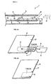
- FIG. 7a is a schematic perspective view of an example of a card-type apparatus.
- Fig. 7b is a schematic cross-sectional view taken along line A-A in Fig. 7a.
- a card-type apparatus 1 is, for example, a PC card or a CF card and includes a circuit substrate 2 and a card-type case 3 accommodating the circuit substrate 2.
- the card-type apparatus 1 is capable of detachably storing a memory card 5, such as a SIM card, in a manner such that the memory card 5 is inserted into the card-type case 3 through a memory card slot 4 formed at one end of a side surface of the card-type case 3, as shown by a dotted line in Fig. 7a.
- the card-type case 3 includes a flat portion 6 disposed on the front substrate surface of the circuit substrate 2 stored in the card-type case 3 with a gap space between the flat portion 6 and the front substrate surface.
- a memory card accommodating space section 8 Part of the gap space between the flat portion 6 and the circuit substrate 2 is a memory card accommodating space section 8 provided for accommodating the memory card 5.
- Terminals 12 are provided in the memory card accommodating space section 8 on the side of the circuit substrate 2, as shown in the schematic cross-sectional view in Fig. 7c, so that when the memory card 5 is stored in the memory card accommodating space section 8, the terminals 12 oppose the memory card 5.
- electrodes 10 for electrically connecting the circuit embedded in the memory card 5 to the outside are provided.
- the terminals 12 are provided so that the terminals 12 correspond to the electrodes 10.
- the terminals 12 contact and connect with the electrodes 10 of the memory card 5 so as to electrically connect the circuits in the memory card 5 with the circuits in the circuit substrate 2.
- the terminals 12 are disposed on the circuit substrate 2 in a manner such that the terminals 12 are disposed on a connector unit 13.
- the terminals 12 are disposed on the upper surface of the connector unit 13.
- the gap space between the terminals 12 and the flat portion 6 may be wider than the thickness d of the memory card 5.
- the memory card 5 if the memory card 5 is inserted and stored in the memory card accommodating space section 8 between the circuit substrate 2 and the flat portion 6, the memory card 5 may be too loose inside the memory card accommodating space section 8.
- the electrodes 10 of the memory card 5 cannot be stably contact and connected with the terminals 12 of the circuit substrate 2.
- the electrical connection between the circuit of the memory card 5 and the circuits of the circuit substrate 2 becomes unstable.
- the card-type apparatus includes a circuit substrate and a card-type case for accommodating the circuit substrate including a flat portion, wherein the flat portion being disposed opposite to one of a front side and a back side of a substrate surface of the circuit substrate with a gap space between the circuit substrate and the flat portion, wherein a part of a gap space between the flat portion of the card-type case and the opposite circuit substrate surface defines a memory card accommodating space section, wherein the memory card is detachably inserted into the memory card accommodating space section from a memory card slot communicating with the memory card accommodating space section along the circuit substrate surface, wherein a terminal for electrically connecting the memory card with the circuit of the circuit substrate is provided on a region of the circuit substrate disposed in the memory card accommodating space section, wherein a plate section for adjusting a gap space between the circuit substrate and the flat portion is disposed at a position opposing the memory card inserted into the memory card accommodating space section
- a plate section for adjusting the gap space is disposed at a position opposing the memory card stored in the memory card accommodating space section.
- the plate section has a protrusion.
- the memory card can be stored inside the memory card accommodating space section while the memory card is contacted with pressure to the terminal of the circuit substrate by the plate section for adjusting the gap space and protrusion on the plate section.
- the simple configuration of providing the plate section for adjusting the gap space and providing the protrusion on the plate section enables the memory card stored in the memory card accommodating space section to be electrically connected to the terminal of the circuit substrate stably by a suitable contact pressure.
- material cost and production cost can be significantly reduced, and stability of the electrical connection between the memory card and the terminals of the circuit substrate can be improved while preventing a reduction in the circuit configuration area.
- the configuration according the present invention is a configuration in which the memory card is connected with contact pressure to the terminals of the circuit substrate by simply providing the plate section for adjusting the gap space and providing the protrusions on the plate section enables the memory card to be electrically connected with contact pressure to the terminal of the circuit substrate.
- the configuration according the present invention does not include an operation mechanism for connecting the memory card to the terminals of the circuit substrate with contact pressure. Therefore, failure of the components for connecting the memory card to the terminals of the circuit substrate with contact pressure hardly occur.
- a card-type apparatus 1 Similar to the card-type apparatus 1 shown in Fig. 7a, a card-type apparatus 1 according to the first embodiment includes a circuit substrate 2 and a card-type case 3 accommodating the circuit substrate 2.
- the card-type apparatus 1 is configured such that a memory card 5 inserted along the substrate surface of the circuit substrate 2 from a memory card slot 4 formed at a side surface of the card-type case 3 is detachably stored in a memory card accommodating space section 8 inside the card-type case 3.
- Fig. 1 is a schematic cross-sectional view illustrating the characteristic components according to the first embodiment.
- Fig. 1 is a cross-sectional view of the card-type apparatus 1 taken along a line positioned at the same position as the line A-A in Fig. 7a is positioned.
- latching units configured to latch the circuit substrate 2 are provided inside the card-type case 3 so as to hold the circuit substrate 2 in the center of the thickness direction of the card-type case 3.
- a plate section 15 for adjusting the gap space between the flat portion 6 and the circuit substrate 2 is provided on a flat portion 6 of the card-type case 3 disposed opposite to the surface of the circuit substrate 2 with a gap space.
- the position of the plate section 15 for adjusting the gap space on the flat portion 6 is a position opposing the memory card 5 inserted in the memory card accommodating space section 8.
- the plate section 15 has protrusions 16 extruded towards the circuit substrate 2 formed by, for example, extruding.
- the components of the card-type apparatus 1 except for the configuration related to the plate section 15 for adjusting the gap space and the protrusions 16 are the same as those of the card-type apparatus 1 shown in Fig. 7a.
- a configuration for ejecting the memory card 5 inserted inside the memory card accommodating space section 8 of the card-type apparatus 1 outside the card-type apparatus 1 is provided in the card-type apparatus 1.
- the configuration is not limited and various configurations may be used. Descriptions of the configurations are omitted here.
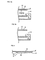
- the flat portion 6 of the card-type case 3 is constituted of a plate member 17 that is composed of, for example, metal, as shown in the schematic perspective view in Fig. 2b.
- the plate member 17, as shown in Fig. 2a, includes a protruding section 17A that protrudes in the removal direction ⁇ of the memory card 5 further than the edge of the card-type case on the inserting end 5s of the memory card 5.
- the base end side of the protrusion of the protruding section 17A is folded inwards to form the plate section 15 for adjusting the gap space.
- the size of the plate section 15 for adjusting the gap space may be the same size as the memory card 5 or may be a size large enough to oppose all of the terminals 12.
- a folded portion K on the base end side of the protruding section 17A constitutes part of an open end of the memory card slot 4, as shown in the schematic cross-sectional view in Fig. 3a.
- the end surface (i.e., a cut surface) of the plate member 17 constitutes part of an open end of the memory card slot 4.
- the end surface of the plate member 17 has minute burrs caused by, for example, cutting. Therefore, for example, when removing or attaching the memory card 5, a person's finger may come into contact with the end surface of the plate member 17 and there is a danger of hurting the finger.
- the folded portion K on the base end side of the protruding section 17A forms part of the open end of the memory card slot 4, and the end (the cut surface) of the protruding section 17A is positioned inside the card-type case 3. Therefore, the end surface of the plate member 17 is most likely prevented from being in contact with a person's finger. In this way, danger caused by the end surface of the plate member 17 can be mostly reduced.
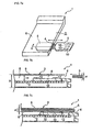
- the protrusions 16 provided on the plate section 15 for adjusting the gap space have a rib configuration extending in the insertion direction ⁇ of the memory card 5 inserted into the memory card accommodating space section 8 from the memory card slot 4.
- a plurality of protrusions 16 is disposed parallel to each other with gap spaces between the protrusions 16.
- the protrusions 16 are provided so as to increase the contact pressure between memory card 5 and the terminals 12 by pushing the memory card 5 stored in the memory card accommodating space section 8 against the terminals 12.
- the terminals 12 are configured so that the terminals 12 apply an urging force to the memory card 5 by elastically deforming due to the pressure from the memory card 5.
- the protrusions 16 are not directly provided on the flat portion 6 but are provided on the plate section 15 for adjusting the gap space that is purposely disposed on the flat portion 6. This is because of the following reason.
- the protrusions 16 are formed by extruding. Therefore, if the protrusions 16 are directly provided on the flat portion 6, depressions caused by the protrusions 16 will be formed on the outer surface of the flat portion 6, causing bad the appearance to be unattractive.
- the plate section 15 for adjusting the gap space is disposed on the back side of the flat portion 6 and cannot be seen from the outer side, by provided the protrusions 16 on the plate section 15 for adjusting the gap space, the problem of unattractive appearance can be prevented.
- the plate section 15 for adjusting the gap space is configured by folding the protruding section 17A provided on the plate member 17 constituting the flat portion 6. Therefore, since both the flat portion 6 and the plate section 15 for adjusting the gap space are composed of the same plate member 17, when the thickness of the flat portion 6 is determined, inevitably, the thickness of the plate section 15 for adjusting the gap space is also determined. In other words, since there is an advantage in that production is facilitated, there is also a disadvantage in that the flexibility (i.e., the flexibility in designing the gap space between the position of the terminals 12 and the plate section 15 for adjusting the gap space) in the design of the gap spaces between the positions of the terminals 12 and the plate section 15 for adjusting the gap space is low.
- the protrusions 16 are provided on the plate section 15 for adjusting the gap space, and there are substantially not limitations for the protrusion height of the protrusions 16, and the flexibility in the design of the protrusions 16 is high. Therefore, by variably adjusting the protrusion height of the protrusions 16, the height of the memory card accommodating space section 8 can be adjusted so that the contact pressure between the memory card 5 and the terminals 12 is suitable for obtaining a reliable electrical connection.
- the protrusions 16 provided on the plate section 15 for adjusting the gap space have a rib configuration extending in the insertion direction ⁇ of the memory card 5 inserted into the memory card accommodating space section 8 from the memory card slot 4. Therefore, when the memory card 5 is moving forward while being inserted into the memory card accommodating space section 8, the memory card 5 will not be caught by the protrusions 16 and can move smoothly forward toward the back side of the memory card accommodating space section 8. In other words, degradation of the insertability of the memory card 5 caused by the protrusions 16 can be prevented.
- the flat portion 6 of the card-type case 3 includes a plate member 17, wherein the plate member 17 includes a protruding section 17A protruding in the removal direction of the memory card 5 further than the edge of the card-type case 3 on the inserting end of the memory card 5, and the base end side of the protrusion of the protruding section 17A is folded inwards to form the plate section 15 for adjusting the gap space. Since the plate section 15 for adjusting the gap space can be easily formed by simply folding the protruding section 17A formed on the plate member 15 of the flat portion 6 inwards to the card-type case 3 at the base end side of the protrusion, the production process can be prevented from becoming complicated.
- the protrusion height of the protrusions 16 provided on the plate section 15 for adjusting the gap space is gradually increased from the memory card slot 4 toward the back side of the memory card accommodating space section 8.
- Other configurations are the same as those according to the first embodiment.
- the protrusion height of the protrusions 16 of the plate section 15 for adjusting the gap space is gradually increased from the memory card slot 4 toward the back side of the memory card accommodating space section 8. Therefore, the following advantage effects can be obtained. More specifically, the protrusion height of the protrusions 16 on the side of the memory card slot 4 is decreased so that the memory card 5 is easily inserted into the memory card accommodating space section 8 from the memory card slot 4. At the same time, the height of the terminals 12 on the side of the memory card accommodating space section 8 causes the memory card 5 to be pressed against the terminals 12 of the circuit substrate 2 so that the contact pressure between the memory card 5 and the terminals 12 of the circuit substrate 2 is increased. In this way, it is easy to achieve both an improvement in the insertability of the memory card 5 and an improvement in the stability of the contact connection between the memory card 5 and the terminals 12.
- the protrusions 16 have a rib configuration extending along the insertion direction ⁇ of the memory card 5.
- the configuration of the protrusions 16 may be, for example, a rib configuration extending in a diagonal direction intersecting the insertion direction ⁇ of the memory card 5, as shown in the plan view in Fig. 5.
- the protrusions 16 may not be linear configuration but may be a point-like configuration or planar configuration.
- the configuration of the protrusions 16 is not limited so long as the contact pressure between the memory card 5 and the terminals 12 can be increased by pressing the memory card 5 against the terminals 12.
- point-like protrusions 16 are provided, for example, the point-like protrusions 16 are disposed at intervals on the plate section 15 for adjusting the gap space. In another example, a plurality of point-like protrusions 16 may be aligned along at least one imaginary line with a space between each other.
- the protrusions 16 are provided only at positions opposite to the memory card 5 stored in the memory card accommodating space section 8.
- the protrusions 16 may be configured so that the protrusions 16 wrap around to the front surface of the flat portion 6 through the open end of the memory card slot 4 from the portion opposing the memory card 5 inserted into the memory card accommodating space section 8. Part of the portion constituting the open end of the memory card slot 4 at the end portion of the flat portion 6 is free to move since it is neither supported nor fixed. Therefore, the mechanical strength is low.
- the protrusions (ribs) 16 are, as shown in the example in Fig.
- the strength of the end portion is improved.
- the protrusions 16 are wrapped around to the front surface of the flat portion 6, as shown in the cross-sectional view in Fig. 6b, similar to the second embodiment, the protrusion height of the protrusions 16 may be increased from the memory card slot 4 toward the back side of the memory card accommodating space section 8.
- the terminals 12 are mounted on the circuit substrate 2 while being mounted on the connector unit 13.
- the terminals 12 may be directly disposed on the substrate surface of the circuit substrate 2.
- the protrusions 16 were formed by extruding.
- the protrusions 16, for example, may be formed by a method other than extruding.
- the plate section 15 for adjusting the gap space is formed by folding back the protruding section 17A provided on the plate member 17 constituting the flat portion 6.
- the plate section 15 for adjusting the gap space may be constituted of a plate member separate from the plate member 17, and then the plate section 15 for adjusting the gap space may be attached to the flat portion 6 (plate member 17) with, for example, an adhesive.
- the thickness of the plate section 15 for adjusting the gap space can be set without being limited by the thickness of the flat portion 6 (plate member 17), and the flexibility of the design can be increased.
- the present invention can be applied to a card-type apparatus having a function for accommodating a memory card.
- the structure of the apparatus is prevented from becoming complicated, and, at the same time, stability of the electrical connection between the memory card and the circuit of the circuit substrate can be obtained. Therefore, the present invention is effective for a card-type apparatus that is required to be compact and low-profile and further provide highly reliable electrical performance while the memory card is inserted in the apparatus.
Abstract
Description
- The present invention relates to a card-type apparatus, such as a CF card, on which a memory card, such as a subscriber identity module (SIM) card, can be attached. Compact Flash (CF) is a trademark registered at the Japanese Patent Office.
- Fig. 7a is a schematic perspective view of an example of a card-type apparatus. Fig. 7b is a schematic cross-sectional view taken along line A-A in Fig. 7a. A card-type apparatus 1 is, for example, a PC card or a CF card and includes a
circuit substrate 2 and a card-type case 3 accommodating thecircuit substrate 2. The card-type apparatus 1 is capable of detachably storing amemory card 5, such as a SIM card, in a manner such that thememory card 5 is inserted into the card-type case 3 through amemory card slot 4 formed at one end of a side surface of the card-type case 3, as shown by a dotted line in Fig. 7a. - More specifically, according to the configuration of the card-type apparatus 1, the card-
type case 3 includes aflat portion 6 disposed on the front substrate surface of thecircuit substrate 2 stored in the card-type case 3 with a gap space between theflat portion 6 and the front substrate surface. Part of the gap space between theflat portion 6 and thecircuit substrate 2 is a memory card accommodatingspace section 8 provided for accommodating thememory card 5.Terminals 12 are provided in the memory card accommodatingspace section 8 on the side of thecircuit substrate 2, as shown in the schematic cross-sectional view in Fig. 7c, so that when thememory card 5 is stored in the memory card accommodatingspace section 8, theterminals 12 oppose thememory card 5. On the card surface of the memory card 5 (the back side of thememory card 5 in Fig. 7a),electrodes 10 for electrically connecting the circuit embedded in thememory card 5 to the outside are provided. Theterminals 12 are provided so that theterminals 12 correspond to theelectrodes 10. When thememory card 5 is stored inside the memory card accommodatingspace section 8, theterminals 12 contact and connect with theelectrodes 10 of thememory card 5 so as to electrically connect the circuits in thememory card 5 with the circuits in thecircuit substrate 2. In the example illustrated in Figs. 7b and 7c, theterminals 12 are disposed on thecircuit substrate 2 in a manner such that theterminals 12 are disposed on aconnector unit 13. - [Patent Document 1]
Japanese Unexamined Patent Application Publication No. 2002-298092 - [Patent Document 2]
Japanese Unexamined Patent Application Publication No. 9-17493 - [Patent Document 3]
Japanese Unexamined Patent Application Publication No. 10-172659 - The thickness D of the card-
type case 3, for example, conforms to a standard. For this reason, when the thickness of thecircuit substrate 2, the height of components for the circuitry mounted on the circuit substrate 2 (especially the height of tall components), and the thickness of theflat portion 6 of the card-type case 3 are taken into consideration, the gap space H between the substrate surface of thecircuit substrate 2 and theflat portion 6 of the card-type case 3 is inevitably determined. The thickness d of thememory card 5, for example, also conforms to a standard. - According to the example illustrated in Fig. 7b, the
terminals 12 are disposed on the upper surface of theconnector unit 13. In some cases, the gap space between theterminals 12 and theflat portion 6 may be wider than the thickness d of thememory card 5. In such a case, if thememory card 5 is inserted and stored in the memory card accommodatingspace section 8 between thecircuit substrate 2 and theflat portion 6, thememory card 5 may be too loose inside the memory card accommodatingspace section 8. In such a case, theelectrodes 10 of thememory card 5 cannot be stably contact and connected with theterminals 12 of thecircuit substrate 2. As a result, the electrical connection between the circuit of thememory card 5 and the circuits of thecircuit substrate 2 becomes unstable. - Accordingly, to prevent such a problem, various configurations for stably and electrically contact connecting the
electrodes 10 of thememory card 5 with theterminals 12 on the side of thecircuit substrate 2 have been proposed. However, the proposed configurations had problems such that they include a large number of components and/or have complicated structures, a circuit configuration area is reduced due to an increase in a area used for the proposed configuration in the card-type case 3, or they have a high production cost causing a difficulty in reducing the cost for the card-type apparatus 1. None of the configurations were satisfactory. - The configuration according to the present invention described below is provided to solve the above-identified problems. More specifically, the card-type apparatus according to the present invention includes a circuit substrate and a card-type case for accommodating the circuit substrate including a flat portion, wherein the flat portion being disposed opposite to one of a front side and a back side of a substrate surface of the circuit substrate with a gap space between the circuit substrate and the flat portion, wherein a part of a gap space between the flat portion of the card-type case and the opposite circuit substrate surface defines a memory card accommodating space section, wherein the memory card is detachably inserted into the memory card accommodating space section from a memory card slot communicating with the memory card accommodating space section along the circuit substrate surface, wherein a terminal for electrically connecting the memory card with the circuit of the circuit substrate is provided on a region of the circuit substrate disposed in the memory card accommodating space section, wherein a plate section for adjusting a gap space between the circuit substrate and the flat portion is disposed at a position opposing the memory card inserted into the memory card accommodating space section on the flat portion of the card-type case, and wherein a protrusion for increasing the contact pressure between the memory card and the terminal by pressing the memory card stored in the memory card accommodating space section against the terminal of the circuit substrate is provided on the plate section.
- According to the present invention, in the flat portion of the card-type case, a plate section for adjusting the gap space is disposed at a position opposing the memory card stored in the memory card accommodating space section. The plate section has a protrusion. According to this configuration, even if the gap space between the flat portion of the card-type case and the circuit substrate stored in the card-type case is determined based on various limitations, the gap space (the height of the memory card accommodating space section) where the memory card is inserted can be adjusted by simply adjusting the thickness of the plate section for adjusting the gap space or the height of the protrusion on the plate section. Accordingly, even if the gap space between the positions of the terminals of the circuit substrate and the flat portion of the card-type case is too wide in comparison with a thickness of the memory card, the memory card can be stored inside the memory card accommodating space section while the memory card is contacted with pressure to the terminal of the circuit substrate by the plate section for adjusting the gap space and protrusion on the plate section.
- In other words, the simple configuration of providing the plate section for adjusting the gap space and providing the protrusion on the plate section enables the memory card stored in the memory card accommodating space section to be electrically connected to the terminal of the circuit substrate stably by a suitable contact pressure. In this way, material cost and production cost can be significantly reduced, and stability of the electrical connection between the memory card and the terminals of the circuit substrate can be improved while preventing a reduction in the circuit configuration area.
- The configuration according the present invention is a configuration in which the memory card is connected with contact pressure to the terminals of the circuit substrate by simply providing the plate section for adjusting the gap space and providing the protrusions on the plate section enables the memory card to be electrically connected with contact pressure to the terminal of the circuit substrate. The configuration according the present invention does not include an operation mechanism for connecting the memory card to the terminals of the circuit substrate with contact pressure. Therefore, failure of the components for connecting the memory card to the terminals of the circuit substrate with contact pressure hardly occur.
-
- Fig. 1 is a cross-sectional view of the characteristic components in a card-type apparatus according to a first embodiment.
- Fig. 2a is a schematic view illustrating, together with Fig. 2b, an exemplary configuration of a flat portion of a card-type case constituting the card-type apparatus according to the first embodiment.
- Fig. 2b is a schematic view illustrating, together with Fig. 2a, an exemplary configuration of a flat portion of a card-type case constituting the card-type apparatus according to the first embodiment.
- Fig. 3a is a schematic view illustrating, together with Fig. 3b, one of the advantages of the configuration according to the first embodiment.
- Fig. 3b is a schematic view illustrating, together with Fig. 3a, one of the advantages of the configuration according to the first embodiment.
- Fig. 4 is a schematic view of the characteristic components in a card-type apparatus according to a second embodiment.
- Fig. 5 is a schematic plan view of protrusions provided on a plate section for adjusting a gap space according to another embodiment.
- Fig. 6a illustrates protrusions according to another embodiment.
- Fig. 6b illustrates protrusions according to another embodiment.
- Fig. 7a is schematic perspective view of an example card-type apparatus.
- Fig. 7b is a schematic cross-sectional view taken along line A-A in Fig. 7a.
- Fig. 7c is a schematic cross-sectional view taken along line A-A in Fig. 7a illustrating a state in which a memory card is stored in a memory card accommodating space section.
-
- 1
- card-type apparatus
- 2
- circuit substrate
- 3
- card-type case
- 4
- memory card slot
- 5
- memory card
- 6
- flat portion
- 8
- memory card accommodating space section
- 12
- terminals
- 15
- plate section for adjusting a gap space
- 16
- protrusions
- Embodiments of the present invention will be described below with reference to the drawings. In the description on the embodiments below, the components that are the same as those of the card-type apparatus 1 shown in Figs. 7a to 7c are represented by the same reference numerals and common parts are not described.
- Similar to the card-type apparatus 1 shown in Fig. 7a, a card-type apparatus 1 according to the first embodiment includes a
circuit substrate 2 and a card-type case 3 accommodating thecircuit substrate 2. The card-type apparatus 1 is configured such that amemory card 5 inserted along the substrate surface of thecircuit substrate 2 from amemory card slot 4 formed at a side surface of the card-type case 3 is detachably stored in a memory card accommodatingspace section 8 inside the card-type case 3. Fig. 1 is a schematic cross-sectional view illustrating the characteristic components according to the first embodiment. Fig. 1 is a cross-sectional view of the card-type apparatus 1 taken along a line positioned at the same position as the line A-A in Fig. 7a is positioned. According to the first embodiment, although not shown in the drawings, latching units configured to latch thecircuit substrate 2 are provided inside the card-type case 3 so as to hold thecircuit substrate 2 in the center of the thickness direction of the card-type case 3. - According to the first embodiment, a
plate section 15 for adjusting the gap space between theflat portion 6 and thecircuit substrate 2 is provided on aflat portion 6 of the card-type case 3 disposed opposite to the surface of thecircuit substrate 2 with a gap space. The position of theplate section 15 for adjusting the gap space on theflat portion 6 is a position opposing thememory card 5 inserted in the memory card accommodatingspace section 8. Theplate section 15 hasprotrusions 16 extruded towards thecircuit substrate 2 formed by, for example, extruding. According to the first embodiment, the components of the card-type apparatus 1 except for the configuration related to theplate section 15 for adjusting the gap space and theprotrusions 16 are the same as those of the card-type apparatus 1 shown in Fig. 7a. A configuration for ejecting thememory card 5 inserted inside the memory card accommodatingspace section 8 of the card-type apparatus 1 outside the card-type apparatus 1 is provided in the card-type apparatus 1. The configuration is not limited and various configurations may be used. Descriptions of the configurations are omitted here. - According to the first embodiment, the
flat portion 6 of the card-type case 3 is constituted of aplate member 17 that is composed of, for example, metal, as shown in the schematic perspective view in Fig. 2b. Theplate member 17, as shown in Fig. 2a, includes a protrudingsection 17A that protrudes in the removal direction α of thememory card 5 further than the edge of the card-type case on the inserting end 5s of thememory card 5. The base end side of the protrusion of the protrudingsection 17A is folded inwards to form theplate section 15 for adjusting the gap space. The size of theplate section 15 for adjusting the gap space may be the same size as thememory card 5 or may be a size large enough to oppose all of theterminals 12. - According to the first embodiment, a folded portion K on the base end side of the protruding
section 17A constitutes part of an open end of thememory card slot 4, as shown in the schematic cross-sectional view in Fig. 3a. On the other hand, conventionally, in some cases, for example, as shown in the diagram in Fig. 3b, the end surface (i.e., a cut surface) of theplate member 17 constitutes part of an open end of thememory card slot 4. The end surface of theplate member 17 has minute burrs caused by, for example, cutting. Therefore, for example, when removing or attaching thememory card 5, a person's finger may come into contact with the end surface of theplate member 17 and there is a danger of hurting the finger. On the other hand, according to the first embodiment, the folded portion K on the base end side of the protrudingsection 17A forms part of the open end of thememory card slot 4, and the end (the cut surface) of the protrudingsection 17A is positioned inside the card-type case 3. Therefore, the end surface of theplate member 17 is most likely prevented from being in contact with a person's finger. In this way, danger caused by the end surface of theplate member 17 can be mostly reduced. - The
protrusions 16 provided on theplate section 15 for adjusting the gap space have a rib configuration extending in the insertion direction α of thememory card 5 inserted into the memory card accommodatingspace section 8 from thememory card slot 4. According to the first embodiment, a plurality ofprotrusions 16 is disposed parallel to each other with gap spaces between theprotrusions 16. Theprotrusions 16 are provided so as to increase the contact pressure betweenmemory card 5 and theterminals 12 by pushing thememory card 5 stored in the memory card accommodatingspace section 8 against theterminals 12. According to the first embodiment, theterminals 12 are configured so that theterminals 12 apply an urging force to thememory card 5 by elastically deforming due to the pressure from thememory card 5. - According to the first embodiment, the
protrusions 16 are not directly provided on theflat portion 6 but are provided on theplate section 15 for adjusting the gap space that is purposely disposed on theflat portion 6. This is because of the following reason. Theprotrusions 16 are formed by extruding. Therefore, if theprotrusions 16 are directly provided on theflat portion 6, depressions caused by theprotrusions 16 will be formed on the outer surface of theflat portion 6, causing bad the appearance to be unattractive. On the other hand, since theplate section 15 for adjusting the gap space is disposed on the back side of theflat portion 6 and cannot be seen from the outer side, by provided theprotrusions 16 on theplate section 15 for adjusting the gap space, the problem of unattractive appearance can be prevented. - According to the first embodiment, the
plate section 15 for adjusting the gap space is configured by folding the protrudingsection 17A provided on theplate member 17 constituting theflat portion 6. Therefore, since both theflat portion 6 and theplate section 15 for adjusting the gap space are composed of thesame plate member 17, when the thickness of theflat portion 6 is determined, inevitably, the thickness of theplate section 15 for adjusting the gap space is also determined. In other words, since there is an advantage in that production is facilitated, there is also a disadvantage in that the flexibility (i.e., the flexibility in designing the gap space between the position of theterminals 12 and theplate section 15 for adjusting the gap space) in the design of the gap spaces between the positions of theterminals 12 and theplate section 15 for adjusting the gap space is low. On the other hand, according to the first embodiment, theprotrusions 16 are provided on theplate section 15 for adjusting the gap space, and there are substantially not limitations for the protrusion height of theprotrusions 16, and the flexibility in the design of theprotrusions 16 is high. Therefore, by variably adjusting the protrusion height of theprotrusions 16, the height of the memory card accommodatingspace section 8 can be adjusted so that the contact pressure between thememory card 5 and theterminals 12 is suitable for obtaining a reliable electrical connection. - According to the first embodiment, the
protrusions 16 provided on theplate section 15 for adjusting the gap space have a rib configuration extending in the insertion direction α of thememory card 5 inserted into the memory card accommodatingspace section 8 from thememory card slot 4. Therefore, when thememory card 5 is moving forward while being inserted into the memory card accommodatingspace section 8, thememory card 5 will not be caught by theprotrusions 16 and can move smoothly forward toward the back side of the memory card accommodatingspace section 8. In other words, degradation of the insertability of thememory card 5 caused by theprotrusions 16 can be prevented. - Moreover, according to the first embodiment, the
flat portion 6 of the card-type case 3 includes aplate member 17, wherein theplate member 17 includes a protrudingsection 17A protruding in the removal direction of thememory card 5 further than the edge of the card-type case 3 on the inserting end of thememory card 5, and the base end side of the protrusion of the protrudingsection 17A is folded inwards to form theplate section 15 for adjusting the gap space. Since theplate section 15 for adjusting the gap space can be easily formed by simply folding the protrudingsection 17A formed on theplate member 15 of theflat portion 6 inwards to the card-type case 3 at the base end side of the protrusion, the production process can be prevented from becoming complicated. - A second embodiment will be described below. In the description for the second embodiment, the components that are the same as those according to the first embodiment are represented by the same reference numerals and the common parts are not described.
- According to the second embodiment, as shown in the schematic cross-sectional view in Fig. 4, the protrusion height of the
protrusions 16 provided on theplate section 15 for adjusting the gap space is gradually increased from thememory card slot 4 toward the back side of the memory card accommodatingspace section 8. Other configurations are the same as those according to the first embodiment. - According to the second embodiment, the protrusion height of the
protrusions 16 of theplate section 15 for adjusting the gap space is gradually increased from thememory card slot 4 toward the back side of the memory card accommodatingspace section 8. Therefore, the following advantage effects can be obtained. More specifically, the protrusion height of theprotrusions 16 on the side of thememory card slot 4 is decreased so that thememory card 5 is easily inserted into the memory card accommodatingspace section 8 from thememory card slot 4. At the same time, the height of theterminals 12 on the side of the memory card accommodatingspace section 8 causes thememory card 5 to be pressed against theterminals 12 of thecircuit substrate 2 so that the contact pressure between thememory card 5 and theterminals 12 of thecircuit substrate 2 is increased. In this way, it is easy to achieve both an improvement in the insertability of thememory card 5 and an improvement in the stability of the contact connection between thememory card 5 and theterminals 12. - The present invention is not limited to the first and second embodiments and may be applied as various different embodiments. For example, according to the first and second embodiments, the
protrusions 16 have a rib configuration extending along the insertion direction α of thememory card 5. However, the configuration of theprotrusions 16 may be, for example, a rib configuration extending in a diagonal direction intersecting the insertion direction α of thememory card 5, as shown in the plan view in Fig. 5. Moreover, theprotrusions 16 may not be linear configuration but may be a point-like configuration or planar configuration. The configuration of theprotrusions 16 is not limited so long as the contact pressure between thememory card 5 and theterminals 12 can be increased by pressing thememory card 5 against theterminals 12. When point-like protrusions 16 are provided, for example, the point-like protrusions 16 are disposed at intervals on theplate section 15 for adjusting the gap space. In another example, a plurality of point-like protrusions 16 may be aligned along at least one imaginary line with a space between each other. - According to the first and second embodiments, the
protrusions 16 are provided only at positions opposite to thememory card 5 stored in the memory card accommodatingspace section 8. However, for example, as shown in the cross-sectional view in Fig. 6a, theprotrusions 16 may be configured so that theprotrusions 16 wrap around to the front surface of theflat portion 6 through the open end of thememory card slot 4 from the portion opposing thememory card 5 inserted into the memory card accommodatingspace section 8. Part of the portion constituting the open end of thememory card slot 4 at the end portion of theflat portion 6 is free to move since it is neither supported nor fixed. Therefore, the mechanical strength is low. However, since the protrusions (ribs) 16 are, as shown in the example in Fig. 6a wrapped around to the outer side of the card from the inner side of the card at the end portion along the end surface, the strength of the end portion is improved. When theprotrusions 16 are wrapped around to the front surface of theflat portion 6, as shown in the cross-sectional view in Fig. 6b, similar to the second embodiment, the protrusion height of theprotrusions 16 may be increased from thememory card slot 4 toward the back side of the memory card accommodatingspace section 8. - According to the first and second embodiments, the
terminals 12 are mounted on thecircuit substrate 2 while being mounted on theconnector unit 13. However, theterminals 12 may be directly disposed on the substrate surface of thecircuit substrate 2. Moreover, according to the first and second embodiments, theprotrusions 16 were formed by extruding. However, theprotrusions 16, for example, may be formed by a method other than extruding. - According to the first and second embodiments, the
plate section 15 for adjusting the gap space is formed by folding back the protrudingsection 17A provided on theplate member 17 constituting theflat portion 6. However, theplate section 15 for adjusting the gap space may be constituted of a plate member separate from theplate member 17, and then theplate section 15 for adjusting the gap space may be attached to the flat portion 6 (plate member 17) with, for example, an adhesive. In such a case, the thickness of theplate section 15 for adjusting the gap space can be set without being limited by the thickness of the flat portion 6 (plate member 17), and the flexibility of the design can be increased. - The present invention can be applied to a card-type apparatus having a function for accommodating a memory card. According to the present invention, the structure of the apparatus is prevented from becoming complicated, and, at the same time, stability of the electrical connection between the memory card and the circuit of the circuit substrate can be obtained. Therefore, the present invention is effective for a card-type apparatus that is required to be compact and low-profile and further provide highly reliable electrical performance while the memory card is inserted in the apparatus.
Claims (6)
- A card-type apparatus comprising:a circuit substrate; anda card-type case for accommodating the circuit substrate including a flat portion, the flat portion being disposed opposite to one of a front side and a back side of a substrate surface of the circuit substrate with a gap space between the circuit substrate and the flat portion,wherein a part of a gap space between the flat portion of the card-type case and the opposite circuit substrate surface defines a memory card accommodating space section,
wherein the memory card is detachably inserted into the memory card accommodating space section from a memory card slot communicating with the memory card accommodating space section along the circuit substrate surface,
wherein a terminal for electrically connecting the memory card with the circuit of the circuit substrate is provided on a region of the circuit substrate in the memory card accommodating space section,
wherein a plate section for adjusting a gap space between the circuit substrate and the flat portion is disposed at a position opposing the memory card inserted into the memory card accommodating space section on the flat portion of the card-type case, and
wherein a protrusion for increasing the contact pressure between the memory card and the terminal by pressing the memory card stored in the memory card accommodating space section against the terminal of the circuit substrate is provided on the plate section. - The card-type apparatus according to Claim 1, wherein the protrusion provided on the plate section for adjusting the gap space have a rib configuration extending in the insertion direction of the memory card inserted into the memory card accommodating space section from the memory card slot.
- The card-type apparatus according to Claim 2, wherein the protrusion height of the protrusion provided on the plate section for adjusting the gap space is gradually increased from the memory card slot toward the deeper end of the memory card accommodating space section.
- The card-type apparatus according to Claim 1,
wherein the flat portion of the card-type case comprises a plate member,
wherein the plate member includes a protruding section protruding in the removal direction of the memory card further than the edge of the card-type case on the inserting end of the memory card, and
wherein the base end side of the protrusion of the protruding section is folded inwards to form the plate section for adjusting the gap space. - The card-type apparatus according to Claim 2,
wherein the flat portion of the card-type case comprises a plate member,
wherein the plate member includes a protruding section protruding in the removal direction of the memory card further than the edge of the card-type case on the inserting end of the memory card, and
wherein the base end side of the protrusion of the protruding section is folded inwards to form the plate section for adjusting the gap space. - The card-type apparatus according to Claim 3,
wherein the flat portion of the card-type case comprises a plate member,
wherein the plate member includes a protruding section protruding in the removal direction of the memory card further than the edge of the card-type case on the inserting end of the memory card, and
wherein the base end side of the protrusion of the protruding section is folded inwards to form the plate section for adjusting the gap space.
Applications Claiming Priority (2)
| Application Number | Priority Date | Filing Date | Title |
|---|---|---|---|
| JP2004264176 | 2004-09-10 | ||
| PCT/JP2005/012945 WO2006027896A1 (en) | 2004-09-10 | 2005-07-13 | Card-type device |
Publications (3)
| Publication Number | Publication Date |
|---|---|
| EP1788511A1 true EP1788511A1 (en) | 2007-05-23 |
| EP1788511A4 EP1788511A4 (en) | 2008-06-11 |
| EP1788511B1 EP1788511B1 (en) | 2012-10-24 |
Family
ID=36036190
Family Applications (1)
| Application Number | Title | Priority Date | Filing Date |
|---|---|---|---|
| EP05765750A Not-in-force EP1788511B1 (en) | 2004-09-10 | 2005-07-13 | Card-type device |
Country Status (7)
| Country | Link |
|---|---|
| US (1) | US7435127B2 (en) |
| EP (1) | EP1788511B1 (en) |
| JP (1) | JP4310470B2 (en) |
| KR (1) | KR100859415B1 (en) |
| CN (1) | CN100565560C (en) |
| TW (1) | TWI316713B (en) |
| WO (1) | WO2006027896A1 (en) |
Families Citing this family (3)
| Publication number | Priority date | Publication date | Assignee | Title |
|---|---|---|---|---|
| US8762640B2 (en) * | 2007-06-27 | 2014-06-24 | Sandisk Il Ltd. | Method for operating a memory interface with SIM functions |
| EP2339502A1 (en) * | 2009-12-21 | 2011-06-29 | Nxp B.V. | Identification card for identifying a user and communication arrangement |
| CN108764382B (en) * | 2018-05-23 | 2021-06-25 | 福建工程学院 | Highway card taking device and working method thereof |
Citations (4)
| Publication number | Priority date | Publication date | Assignee | Title |
|---|---|---|---|---|
| GB2226192A (en) * | 1988-11-09 | 1990-06-20 | Sagem | Chip card receiver |
| EP0704813A2 (en) * | 1994-09-29 | 1996-04-03 | Kabushiki Kaisha Toshiba | Ic card information processing apparatus |
| US5877488A (en) * | 1996-04-22 | 1999-03-02 | Stocko Metallwarenfabriken Henkels Und Sohn Gmbh | Combination chip card reader |
| US6069795A (en) * | 1995-04-01 | 2000-05-30 | Stocko Metallwarenfabriken | PCMCIA card for receiving and contacting a chip card |
Family Cites Families (7)
| Publication number | Priority date | Publication date | Assignee | Title |
|---|---|---|---|---|
| JP3121747B2 (en) | 1995-06-27 | 2001-01-09 | ヒロセ電機株式会社 | Card connector with surface contacts |
| EP0803834A3 (en) * | 1996-04-25 | 2000-06-28 | Olympus Optical Co., Ltd. | Memory card installing device |
| JPH10172659A (en) | 1996-12-06 | 1998-06-26 | Japan Aviation Electron Ind Ltd | Ejector housing type card connector equipped with stopper |
| JP2002298092A (en) | 2001-03-30 | 2002-10-11 | Matsushita Electric Ind Co Ltd | Pc card |
| JP3812939B2 (en) * | 2002-04-09 | 2006-08-23 | 日本航空電子工業株式会社 | Card connector |
| JP2003331223A (en) | 2002-05-13 | 2003-11-21 | Infotrust Inc | Card reader, battery pack and portable terminal |
| US6951472B2 (en) * | 2003-11-17 | 2005-10-04 | P-Two Industries Inc. | Lift-cover memory card connector |
-
2005
- 2005-07-11 TW TW094123358A patent/TWI316713B/en not_active IP Right Cessation
- 2005-07-13 EP EP05765750A patent/EP1788511B1/en not_active Not-in-force
- 2005-07-13 US US11/574,650 patent/US7435127B2/en not_active Expired - Fee Related
- 2005-07-13 WO PCT/JP2005/012945 patent/WO2006027896A1/en active Application Filing
- 2005-07-13 CN CNB200580029777XA patent/CN100565560C/en not_active Expired - Fee Related
- 2005-07-13 JP JP2006535063A patent/JP4310470B2/en not_active Expired - Fee Related
- 2005-07-13 KR KR1020077005332A patent/KR100859415B1/en not_active IP Right Cessation
Patent Citations (4)
| Publication number | Priority date | Publication date | Assignee | Title |
|---|---|---|---|---|
| GB2226192A (en) * | 1988-11-09 | 1990-06-20 | Sagem | Chip card receiver |
| EP0704813A2 (en) * | 1994-09-29 | 1996-04-03 | Kabushiki Kaisha Toshiba | Ic card information processing apparatus |
| US6069795A (en) * | 1995-04-01 | 2000-05-30 | Stocko Metallwarenfabriken | PCMCIA card for receiving and contacting a chip card |
| US5877488A (en) * | 1996-04-22 | 1999-03-02 | Stocko Metallwarenfabriken Henkels Und Sohn Gmbh | Combination chip card reader |
Non-Patent Citations (1)
| Title |
|---|
| See also references of WO2006027896A1 * |
Also Published As
| Publication number | Publication date |
|---|---|
| US20080009174A1 (en) | 2008-01-10 |
| EP1788511B1 (en) | 2012-10-24 |
| CN101010680A (en) | 2007-08-01 |
| WO2006027896A1 (en) | 2006-03-16 |
| EP1788511A4 (en) | 2008-06-11 |
| TWI316713B (en) | 2009-11-01 |
| KR100859415B1 (en) | 2008-09-22 |
| KR20070051303A (en) | 2007-05-17 |
| US7435127B2 (en) | 2008-10-14 |
| JPWO2006027896A1 (en) | 2008-05-08 |
| CN100565560C (en) | 2009-12-02 |
| JP4310470B2 (en) | 2009-08-12 |
| TW200627464A (en) | 2006-08-01 |
Similar Documents
| Publication | Publication Date | Title |
|---|---|---|
| US8113872B2 (en) | Flat-cable connector, production process thereof, and locking device | |
| US7056146B2 (en) | Insulation displacement contact and electric connector using the same | |
| US6947767B2 (en) | Card holding structure and portable terminal apparatus having the same | |
| US7527532B2 (en) | Battery contact | |
| JP5852056B2 (en) | Card connectors and contacts | |
| US20070275601A1 (en) | Card Connector And Method For Producing Housing Assembly | |
| US7744421B2 (en) | Card connector and method of assembling same | |
| JP2007234472A (en) | Card connector | |
| JPH07326416A (en) | Terminal and connector | |
| CN100536239C (en) | Card connector | |
| EP1788511A1 (en) | Card-type device | |
| EP1381116B1 (en) | Sprung electrical terminal | |
| JP4851667B2 (en) | Card connector | |
| JP4571028B2 (en) | Card connector | |
| KR100519462B1 (en) | Contact Pin and SIM Slide Connector with Them | |
| CN111244656A (en) | Miniature terminal assembly | |
| KR102066957B1 (en) | Connector for card | |
| WO2019108530A1 (en) | Card socket | |
| JP2003331975A (en) | Fixing structure of card connector | |
| CN211320377U (en) | Miniature terminal assembly | |
| JP2017045678A (en) | Card connector | |
| KR101969381B1 (en) | Card connector | |
| JP2004152541A (en) | Memory card connector | |
| JP2008204847A (en) | Card connector device | |
| JP2002373736A (en) | Electric connector |
Legal Events
| Date | Code | Title | Description |
|---|---|---|---|
| PUAI | Public reference made under article 153(3) epc to a published international application that has entered the european phase |
Free format text: ORIGINAL CODE: 0009012 |
|
| 17P | Request for examination filed |
Effective date: 20070105 |
|
| AK | Designated contracting states |
Kind code of ref document: A1 Designated state(s): AT BE BG CH CY CZ DE DK EE ES FI FR GB GR HU IE IS IT LI LT LU LV MC NL PL PT RO SE SI SK TR |
|
| DAX | Request for extension of the european patent (deleted) | ||
| A4 | Supplementary search report drawn up and despatched |
Effective date: 20080514 |
|
| 17Q | First examination report despatched |
Effective date: 20080715 |
|
| GRAP | Despatch of communication of intention to grant a patent |
Free format text: ORIGINAL CODE: EPIDOSNIGR1 |
|
| RIC1 | Information provided on ipc code assigned before grant |
Ipc: G06K 7/00 20060101ALI20120416BHEP Ipc: G06K 19/077 20060101ALI20120416BHEP Ipc: B42D 15/10 20060101ALI20120416BHEP Ipc: G06K 17/00 20060101AFI20120416BHEP |
|
| GRAS | Grant fee paid |
Free format text: ORIGINAL CODE: EPIDOSNIGR3 |
|
| GRAA | (expected) grant |
Free format text: ORIGINAL CODE: 0009210 |
|
| AK | Designated contracting states |
Kind code of ref document: B1 Designated state(s): AT BE BG CH CY CZ DE DK EE ES FI FR GB GR HU IE IS IT LI LT LU LV MC NL PL PT RO SE SI SK TR |
|
| REG | Reference to a national code |
Ref country code: GB Ref legal event code: FG4D |
|
| REG | Reference to a national code |
Ref country code: CH Ref legal event code: EP |
|
| REG | Reference to a national code |
Ref country code: AT Ref legal event code: REF Ref document number: 581264 Country of ref document: AT Kind code of ref document: T Effective date: 20121115 |
|
| REG | Reference to a national code |
Ref country code: IE Ref legal event code: FG4D |
|
| REG | Reference to a national code |
Ref country code: DE Ref legal event code: R096 Ref document number: 602005036702 Country of ref document: DE Effective date: 20121220 |
|
| REG | Reference to a national code |
Ref country code: AT Ref legal event code: MK05 Ref document number: 581264 Country of ref document: AT Kind code of ref document: T Effective date: 20121024 |
|
| REG | Reference to a national code |
Ref country code: NL Ref legal event code: VDEP Effective date: 20121024 |
|
| PG25 | Lapsed in a contracting state [announced via postgrant information from national office to epo] |
Ref country code: FI Free format text: LAPSE BECAUSE OF FAILURE TO SUBMIT A TRANSLATION OF THE DESCRIPTION OR TO PAY THE FEE WITHIN THE PRESCRIBED TIME-LIMIT Effective date: 20121024 Ref country code: SE Free format text: LAPSE BECAUSE OF FAILURE TO SUBMIT A TRANSLATION OF THE DESCRIPTION OR TO PAY THE FEE WITHIN THE PRESCRIBED TIME-LIMIT Effective date: 20121024 Ref country code: NL Free format text: LAPSE BECAUSE OF FAILURE TO SUBMIT A TRANSLATION OF THE DESCRIPTION OR TO PAY THE FEE WITHIN THE PRESCRIBED TIME-LIMIT Effective date: 20121024 Ref country code: ES Free format text: LAPSE BECAUSE OF FAILURE TO SUBMIT A TRANSLATION OF THE DESCRIPTION OR TO PAY THE FEE WITHIN THE PRESCRIBED TIME-LIMIT Effective date: 20130204 Ref country code: IS Free format text: LAPSE BECAUSE OF FAILURE TO SUBMIT A TRANSLATION OF THE DESCRIPTION OR TO PAY THE FEE WITHIN THE PRESCRIBED TIME-LIMIT Effective date: 20130224 |
|
| PG25 | Lapsed in a contracting state [announced via postgrant information from national office to epo] |
Ref country code: PL Free format text: LAPSE BECAUSE OF FAILURE TO SUBMIT A TRANSLATION OF THE DESCRIPTION OR TO PAY THE FEE WITHIN THE PRESCRIBED TIME-LIMIT Effective date: 20121024 Ref country code: SI Free format text: LAPSE BECAUSE OF FAILURE TO SUBMIT A TRANSLATION OF THE DESCRIPTION OR TO PAY THE FEE WITHIN THE PRESCRIBED TIME-LIMIT Effective date: 20121024 Ref country code: PT Free format text: LAPSE BECAUSE OF FAILURE TO SUBMIT A TRANSLATION OF THE DESCRIPTION OR TO PAY THE FEE WITHIN THE PRESCRIBED TIME-LIMIT Effective date: 20130225 Ref country code: LV Free format text: LAPSE BECAUSE OF FAILURE TO SUBMIT A TRANSLATION OF THE DESCRIPTION OR TO PAY THE FEE WITHIN THE PRESCRIBED TIME-LIMIT Effective date: 20121024 Ref country code: BE Free format text: LAPSE BECAUSE OF FAILURE TO SUBMIT A TRANSLATION OF THE DESCRIPTION OR TO PAY THE FEE WITHIN THE PRESCRIBED TIME-LIMIT Effective date: 20121024 Ref country code: CY Free format text: LAPSE BECAUSE OF FAILURE TO SUBMIT A TRANSLATION OF THE DESCRIPTION OR TO PAY THE FEE WITHIN THE PRESCRIBED TIME-LIMIT Effective date: 20121024 Ref country code: GR Free format text: LAPSE BECAUSE OF FAILURE TO SUBMIT A TRANSLATION OF THE DESCRIPTION OR TO PAY THE FEE WITHIN THE PRESCRIBED TIME-LIMIT Effective date: 20130125 |
|
| PG25 | Lapsed in a contracting state [announced via postgrant information from national office to epo] |
Ref country code: AT Free format text: LAPSE BECAUSE OF FAILURE TO SUBMIT A TRANSLATION OF THE DESCRIPTION OR TO PAY THE FEE WITHIN THE PRESCRIBED TIME-LIMIT Effective date: 20121024 |
|
| PG25 | Lapsed in a contracting state [announced via postgrant information from national office to epo] |
Ref country code: BG Free format text: LAPSE BECAUSE OF FAILURE TO SUBMIT A TRANSLATION OF THE DESCRIPTION OR TO PAY THE FEE WITHIN THE PRESCRIBED TIME-LIMIT Effective date: 20130124 Ref country code: DK Free format text: LAPSE BECAUSE OF FAILURE TO SUBMIT A TRANSLATION OF THE DESCRIPTION OR TO PAY THE FEE WITHIN THE PRESCRIBED TIME-LIMIT Effective date: 20121024 Ref country code: SK Free format text: LAPSE BECAUSE OF FAILURE TO SUBMIT A TRANSLATION OF THE DESCRIPTION OR TO PAY THE FEE WITHIN THE PRESCRIBED TIME-LIMIT Effective date: 20121024 Ref country code: EE Free format text: LAPSE BECAUSE OF FAILURE TO SUBMIT A TRANSLATION OF THE DESCRIPTION OR TO PAY THE FEE WITHIN THE PRESCRIBED TIME-LIMIT Effective date: 20121024 Ref country code: CZ Free format text: LAPSE BECAUSE OF FAILURE TO SUBMIT A TRANSLATION OF THE DESCRIPTION OR TO PAY THE FEE WITHIN THE PRESCRIBED TIME-LIMIT Effective date: 20121024 |
|
| PG25 | Lapsed in a contracting state [announced via postgrant information from national office to epo] |
Ref country code: RO Free format text: LAPSE BECAUSE OF FAILURE TO SUBMIT A TRANSLATION OF THE DESCRIPTION OR TO PAY THE FEE WITHIN THE PRESCRIBED TIME-LIMIT Effective date: 20121024 Ref country code: IT Free format text: LAPSE BECAUSE OF FAILURE TO SUBMIT A TRANSLATION OF THE DESCRIPTION OR TO PAY THE FEE WITHIN THE PRESCRIBED TIME-LIMIT Effective date: 20121024 |
|
| PLBE | No opposition filed within time limit |
Free format text: ORIGINAL CODE: 0009261 |
|
| STAA | Information on the status of an ep patent application or granted ep patent |
Free format text: STATUS: NO OPPOSITION FILED WITHIN TIME LIMIT |
|
| 26N | No opposition filed |
Effective date: 20130725 |
|
| REG | Reference to a national code |
Ref country code: DE Ref legal event code: R097 Ref document number: 602005036702 Country of ref document: DE Effective date: 20130725 |
|
| PG25 | Lapsed in a contracting state [announced via postgrant information from national office to epo] |
Ref country code: MC Free format text: LAPSE BECAUSE OF FAILURE TO SUBMIT A TRANSLATION OF THE DESCRIPTION OR TO PAY THE FEE WITHIN THE PRESCRIBED TIME-LIMIT Effective date: 20121024 |
|
| REG | Reference to a national code |
Ref country code: CH Ref legal event code: PL |
|
| REG | Reference to a national code |
Ref country code: IE Ref legal event code: MM4A |
|
| PG25 | Lapsed in a contracting state [announced via postgrant information from national office to epo] |
Ref country code: CH Free format text: LAPSE BECAUSE OF NON-PAYMENT OF DUE FEES Effective date: 20130731 Ref country code: LI Free format text: LAPSE BECAUSE OF NON-PAYMENT OF DUE FEES Effective date: 20130731 |
|
| PG25 | Lapsed in a contracting state [announced via postgrant information from national office to epo] |
Ref country code: LT Free format text: LAPSE BECAUSE OF FAILURE TO SUBMIT A TRANSLATION OF THE DESCRIPTION OR TO PAY THE FEE WITHIN THE PRESCRIBED TIME-LIMIT Effective date: 20121024 Ref country code: IE Free format text: LAPSE BECAUSE OF NON-PAYMENT OF DUE FEES Effective date: 20130713 |
|
| PGFP | Annual fee paid to national office [announced via postgrant information from national office to epo] |
Ref country code: DE Payment date: 20140709 Year of fee payment: 10 |
|
| PGFP | Annual fee paid to national office [announced via postgrant information from national office to epo] |
Ref country code: GB Payment date: 20140709 Year of fee payment: 10 Ref country code: FR Payment date: 20140708 Year of fee payment: 10 |
|
| PG25 | Lapsed in a contracting state [announced via postgrant information from national office to epo] |
Ref country code: TR Free format text: LAPSE BECAUSE OF FAILURE TO SUBMIT A TRANSLATION OF THE DESCRIPTION OR TO PAY THE FEE WITHIN THE PRESCRIBED TIME-LIMIT Effective date: 20121024 |
|
| PG25 | Lapsed in a contracting state [announced via postgrant information from national office to epo] |
Ref country code: LU Free format text: LAPSE BECAUSE OF NON-PAYMENT OF DUE FEES Effective date: 20130713 Ref country code: HU Free format text: LAPSE BECAUSE OF FAILURE TO SUBMIT A TRANSLATION OF THE DESCRIPTION OR TO PAY THE FEE WITHIN THE PRESCRIBED TIME-LIMIT; INVALID AB INITIO Effective date: 20050713 |
|
| REG | Reference to a national code |
Ref country code: DE Ref legal event code: R119 Ref document number: 602005036702 Country of ref document: DE |
|
| GBPC | Gb: european patent ceased through non-payment of renewal fee |
Effective date: 20150713 |
|
| PG25 | Lapsed in a contracting state [announced via postgrant information from national office to epo] |
Ref country code: DE Free format text: LAPSE BECAUSE OF NON-PAYMENT OF DUE FEES Effective date: 20160202 Ref country code: GB Free format text: LAPSE BECAUSE OF NON-PAYMENT OF DUE FEES Effective date: 20150713 |
|
| REG | Reference to a national code |
Ref country code: FR Ref legal event code: ST Effective date: 20160331 |
|
| PG25 | Lapsed in a contracting state [announced via postgrant information from national office to epo] |
Ref country code: FR Free format text: LAPSE BECAUSE OF NON-PAYMENT OF DUE FEES Effective date: 20150731 |