EP1764343A2 - Method for etching a structured cavity with a single mask - Google Patents
Method for etching a structured cavity with a single mask Download PDFInfo
- Publication number
- EP1764343A2 EP1764343A2 EP06120739A EP06120739A EP1764343A2 EP 1764343 A2 EP1764343 A2 EP 1764343A2 EP 06120739 A EP06120739 A EP 06120739A EP 06120739 A EP06120739 A EP 06120739A EP 1764343 A2 EP1764343 A2 EP 1764343A2
- Authority
- EP
- European Patent Office
- Prior art keywords
- mask
- substrate
- cavity
- etch
- pattern
- Prior art date
- Legal status (The legal status is an assumption and is not a legal conclusion. Google has not performed a legal analysis and makes no representation as to the accuracy of the status listed.)
- Withdrawn
Links
- 238000000034 method Methods 0.000 title claims description 56
- 238000005530 etching Methods 0.000 title claims description 27
- 239000000758 substrate Substances 0.000 claims abstract description 65
- 239000012528 membrane Substances 0.000 claims abstract description 12
- 238000004519 manufacturing process Methods 0.000 claims abstract description 7
- 238000000708 deep reactive-ion etching Methods 0.000 claims description 26
- 229920002120 photoresistant polymer Polymers 0.000 claims description 15
- SFZCNBIFKDRMGX-UHFFFAOYSA-N sulfur hexafluoride Chemical compound FS(F)(F)(F)(F)F SFZCNBIFKDRMGX-UHFFFAOYSA-N 0.000 claims description 11
- 238000009616 inductively coupled plasma Methods 0.000 claims description 9
- VYPSYNLAJGMNEJ-UHFFFAOYSA-N Silicium dioxide Chemical compound O=[Si]=O VYPSYNLAJGMNEJ-UHFFFAOYSA-N 0.000 claims description 7
- 229910052814 silicon oxide Inorganic materials 0.000 claims description 7
- 229910052710 silicon Inorganic materials 0.000 claims description 4
- 239000010703 silicon Substances 0.000 claims description 4
- 239000000463 material Substances 0.000 claims description 3
- 229910052581 Si3N4 Inorganic materials 0.000 claims description 2
- 238000001312 dry etching Methods 0.000 claims description 2
- 150000002500 ions Chemical class 0.000 claims description 2
- HQVNEWCFYHHQES-UHFFFAOYSA-N silicon nitride Chemical compound N12[Si]34N5[Si]62N3[Si]51N64 HQVNEWCFYHHQES-UHFFFAOYSA-N 0.000 claims description 2
- 229960000909 sulfur hexafluoride Drugs 0.000 claims description 2
- 238000010586 diagram Methods 0.000 description 21
- 238000001878 scanning electron micrograph Methods 0.000 description 11
- 239000002184 metal Substances 0.000 description 8
- 229910052751 metal Inorganic materials 0.000 description 8
- 238000012545 processing Methods 0.000 description 7
- 238000002161 passivation Methods 0.000 description 6
- 238000000206 photolithography Methods 0.000 description 6
- 239000010410 layer Substances 0.000 description 5
- XUIMIQQOPSSXEZ-UHFFFAOYSA-N Silicon Chemical compound [Si] XUIMIQQOPSSXEZ-UHFFFAOYSA-N 0.000 description 4
- 230000003628 erosive effect Effects 0.000 description 3
- 238000001020 plasma etching Methods 0.000 description 3
- 238000013459 approach Methods 0.000 description 2
- 238000001816 cooling Methods 0.000 description 2
- 230000000694 effects Effects 0.000 description 2
- 229910052731 fluorine Inorganic materials 0.000 description 2
- 239000011737 fluorine Substances 0.000 description 2
- 238000000227 grinding Methods 0.000 description 2
- 239000007788 liquid Substances 0.000 description 2
- 239000007921 spray Substances 0.000 description 2
- 238000005507 spraying Methods 0.000 description 2
- WGTYBPLFGIVFAS-UHFFFAOYSA-M tetramethylammonium hydroxide Chemical compound [OH-].C[N+](C)(C)C WGTYBPLFGIVFAS-UHFFFAOYSA-M 0.000 description 2
- 238000009623 Bosch process Methods 0.000 description 1
- YCKRFDGAMUMZLT-UHFFFAOYSA-N Fluorine atom Chemical compound [F] YCKRFDGAMUMZLT-UHFFFAOYSA-N 0.000 description 1
- -1 Fluorine ions Chemical class 0.000 description 1
- 239000003990 capacitor Substances 0.000 description 1
- 239000011248 coating agent Substances 0.000 description 1
- 238000000576 coating method Methods 0.000 description 1
- 238000013461 design Methods 0.000 description 1
- 238000005516 engineering process Methods 0.000 description 1
- 239000007789 gas Substances 0.000 description 1
- 239000011521 glass Substances 0.000 description 1
- 239000001307 helium Substances 0.000 description 1
- 229910052734 helium Inorganic materials 0.000 description 1
- SWQJXJOGLNCZEY-UHFFFAOYSA-N helium atom Chemical compound [He] SWQJXJOGLNCZEY-UHFFFAOYSA-N 0.000 description 1
- 238000011065 in-situ storage Methods 0.000 description 1
- 239000011261 inert gas Substances 0.000 description 1
- 230000007774 longterm Effects 0.000 description 1
- 230000003071 parasitic effect Effects 0.000 description 1
- 238000000059 patterning Methods 0.000 description 1
- 230000000704 physical effect Effects 0.000 description 1
- 230000001681 protective effect Effects 0.000 description 1
- 239000011241 protective layer Substances 0.000 description 1
- 238000004544 sputter deposition Methods 0.000 description 1
- 238000010561 standard procedure Methods 0.000 description 1
Images


Classifications
-
- B—PERFORMING OPERATIONS; TRANSPORTING
- B81—MICROSTRUCTURAL TECHNOLOGY
- B81C—PROCESSES OR APPARATUS SPECIALLY ADAPTED FOR THE MANUFACTURE OR TREATMENT OF MICROSTRUCTURAL DEVICES OR SYSTEMS
- B81C1/00—Manufacture or treatment of devices or systems in or on a substrate
- B81C1/00015—Manufacture or treatment of devices or systems in or on a substrate for manufacturing microsystems
- B81C1/00023—Manufacture or treatment of devices or systems in or on a substrate for manufacturing microsystems without movable or flexible elements
- B81C1/00119—Arrangement of basic structures like cavities or channels, e.g. suitable for microfluidic systems
-
- B—PERFORMING OPERATIONS; TRANSPORTING
- B81—MICROSTRUCTURAL TECHNOLOGY
- B81B—MICROSTRUCTURAL DEVICES OR SYSTEMS, e.g. MICROMECHANICAL DEVICES
- B81B2201/00—Specific applications of microelectromechanical systems
- B81B2201/02—Sensors
- B81B2201/0257—Microphones or microspeakers
-
- B—PERFORMING OPERATIONS; TRANSPORTING
- B81—MICROSTRUCTURAL TECHNOLOGY
- B81B—MICROSTRUCTURAL DEVICES OR SYSTEMS, e.g. MICROMECHANICAL DEVICES
- B81B2203/00—Basic microelectromechanical structures
- B81B2203/01—Suspended structures, i.e. structures allowing a movement
- B81B2203/0127—Diaphragms, i.e. structures separating two media that can control the passage from one medium to another; Membranes, i.e. diaphragms with filtering function
-
- B—PERFORMING OPERATIONS; TRANSPORTING
- B81—MICROSTRUCTURAL TECHNOLOGY
- B81B—MICROSTRUCTURAL DEVICES OR SYSTEMS, e.g. MICROMECHANICAL DEVICES
- B81B2203/00—Basic microelectromechanical structures
- B81B2203/03—Static structures
- B81B2203/0315—Cavities
-
- B—PERFORMING OPERATIONS; TRANSPORTING
- B81—MICROSTRUCTURAL TECHNOLOGY
- B81B—MICROSTRUCTURAL DEVICES OR SYSTEMS, e.g. MICROMECHANICAL DEVICES
- B81B2203/00—Basic microelectromechanical structures
- B81B2203/03—Static structures
- B81B2203/0353—Holes
Definitions
- This invention relates to the field of MEM (microelectromechanical) devices, and in particular to a method of making an etched structure in such devices.
- MEM microelectromechanical
- micro microphone as a microelectomechanical systems (MEMS) device
- MEMS microelectomechanical systems
- a simple way to create this structure is to etch deep holes through the metal grid, flip the substrate up side down and etch the cavity, (or vice-versa).
- ICP Inductively Coupled Plasma
- DRIE Deep Reactive Ion Etching
- the main disadvantage with this approach lies in the step where the metal is exposed to the plasma when etching through the metal grid because metal sputtering can impair the properties of the ICP reactor. This causes a long-term drift of the etching characteristics as the metal is sputtered on the chamber walls. The coating of the chamber walls with the sputtered metal causes a parasitic capacitor that changes the impedance of the chamber. This parameter is essential for a good control of the etch profiles.
- Isotropic and anisotropic plasma etching is widely used to fabricate micro-machined structures and devices. They are generally used separately to remove or define some geometry in a specific layer. The geometries are generally defined with photolithography technique that leaves the image of the photolithographic mask in a photoresist. This pattern is then duplicated by etching one or a few layers under it using different etching techniques.
- MEMS processes generally use deep reactive ion etching (DRIE) to form structures with high aspect ratios.
- DRIE deep reactive ion etching
- the geometries are generally critical in such systems, and non-conventional approaches are often utilised to get the desired shape.
- Different anisotropic techniques were previously invented using different shrewdness to accomplish etch shapes with high aspect ratios. This is either done by carefully adjust etching and passivation species, by switching etching and passivation species alternatively or by using physical bombardment or intrinsic physical properties of the substrate to create a directionality [e.g. TMAH etching].
- One object of the present invention is to form an etched pattern in the bottom of a cavity.
- Various techniques were considered.
- One such technique is wafer bonding.
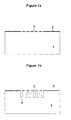
- Figs. 1a to Fig. 1f summarize the process.
- This solution is expensive since two substrates are needed and the cavity substrate often needs to be back grinded to get the desired thickness or to open the cavity. The later leads into a depth of the cavity difficult to control and leads to large variation across the wafer.
- a second technique uses the spray coating technique. It starts first with an anisotropic or isotropic etch to create the desire cavity (Fig. 2a to 2b), then is followed by the removal of the etching mask (Fig.2c). Then, a spray coater is used to coat the walls and the bottom of the cavity with photoresist (Fig. 2d). A photolithography mask aligner able to project the photolithography mask image in the bottom of the cavity without distortion (with a large depth of field) is then used to create the pattern in the bottom of the cavity (Fig.2e). Finally, DRIE (Deep Reactive Ion Etch) is used to imprint the pattern in the bottom of the cavity (fig.2f). This technique is greatly limited in the depth of the cavity. Greater the depth of the cavity worse is the resolution of the pattern in the bottom of the cavity.
- DRIE Deep Reactive Ion Etch
- a third technique is possible when the pattern in the bottom of the cavity is extended throughout the whole substrate. This can be accomplished by creating the cavity on one side of the substrate with the desired depth (Fig.2d), and then the substrate is flipped over and a second mask is patterned on the other side (aligned with the first one: Fig.3a). Finally, the DRIE is used to etch the pattern and reach the cavity (Fig. 3b). Either the cavity or the pattern can be done first. This solution implies handling of the two side of the wafer and the thickness of the substrate need to be very uniform. Furthermore, when etching the second side (either the cavity or the pattern), at the point where the cavity depth reach the "bottom" of the etched pattern or vice versa, lost of dimensions is generally seen.
- a second wafer substrate is needed, with optional back grinding if a specific thickness is needed.
- the invention provides a method of forming a micro-machined structure in a substrate, by etching a cavity in the substrate under a protective mask and etching the pattern of the mask in the bottom of the cavity using dry plasma etching technique.
- This uses a single mask to form both a cavity and the etched structures imprinted in the bottom of the cavity.
- the method includes optionally forming at least one micro-machined structure, in which a mask with the necessary minimum strain is used to etch the substrate and create a cavity under the mask.
- the pattern of the mask is then duplicated in the bottom of the cavity using the DRIE. This leaves a suspended membrane on top of the cavity, which can be optionally stripped away with a selective, etch.
- the present invention provides a method of making an etch structure in a substrate comprising providing a mask on the substrate with a pattern that leaves at least one opening exposing the substrate to the ambient; performing an isotropic or quasi-isotropic etch through the mask to create a cavity under the mask, which mask is left behind as a suspended membrane above the cavity; and performing a subsequent anisotropic etch that etches anisotropically a pattern of holes corrsponding to the pattern of the mask in the bottom of the cavity.
- the method according to the present invention has an advantage over the related art that creates pattern in the bottom of the cavity since only one patterned mask is necessary.
- the method intended in the present invention contains three main steps.
- the mask can be removed by selective stripping.
- the shape of the cavity is determined by the desired pattern in the bottom of the cavity. Also the sharpness of the sidewalls of the pattern in the bottom of the cavity is more difficult to obtain as with standard DRIE processes, so the process needs to be well tuned in order to minimize diversion of enchants during DRIE etching. Otherwise, enlargement of the structure is seen in the reproduced etch pattern.
- the invention is particularly applicable to the manufacture of micro microphones, but one skilled in the art will appreciate that it can be applied to the fabrication of other like structures.
- Figure 1 a is a diagram of the openings made in a photoresist mask on the first substrate
- Figure 1b is a diagram of the substrate in Fig. 1a after DRIE etching of the pattern
- Figure 1c is a diagram of the 2nd substrate with openings for the cavity mask
- Figure 1d is a diagram of the 2nd substrate after etching of the cavity
- Figure 1e is a diagram of the bonding of the two substrates shown in Fig. 1d and 1b;
- Figure If is a diagram of the two bonded substratew after back grinding
- Figure 2a is a diagram of the substrate with openings in a photoresist mask (the cavity mask);
- Figure 2b is a diagram of the substrate after etching of the cavity
- Figure 2c is a diagram of the substrate after stripping of the resist
- Figure 2d is a diagram of the substrate after spray coating photoresist
- Figure 2e is a diagram of the substrate after exposing and developing of the spray coated photoresist
- Figure 2f is a diagram of the substrate after DRIE etching of the pattern in Fig 2e;
- Figure 3a is a diagram of the substrate shown in 2b after flip out-side-down and photolithography on the backside;
- Figure 3b is a diagram of the substrate shown in 3a after DRIE etching of the pattern in Fig.3a;
- Figure4 is a diagram of the substrate covered with the mask film (Cross section and Top view);
- Figure 5 is a diagram of the openings made in the mask. (Cross section and Top view);
- Figure 6a is a diagram of isotropic etch of the bulk substrate
- Figure 6b is a diagram of the cavity etched under the mask (Cross section and Top view);
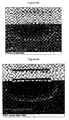
- Figure 6c is a SEM image of a cavity etched under a photoresist mask
- Figure 6d is a SEM image of a cavity etched under a silicon oxide mask
- Figure 7a is a diagram of the etched structure created by DRIE in the bottom of the cavity
- Figure 7b is a SEM image of an etched pattern in the bottom of the cavity using photoresist mask
- Figure 7c is a SEM image of an etched pattern in the bottom of the cavity using silicon oxide mask
- Figure 7d is a SEM image of an etched pattern in the bottom of the cavity using silicon oxide mask
- Figure 8a is a diagram of the micro-machined structure after stripping of the mask layer
- Figure 8b is a SEM image of a micro-machined structure after stripping
- Fig. 9a is a diagram of the micro-machined structure with an etch stop layer.
- Fig. 9b is a SEM image of a micro-machined structure with an etch stop layer.
- Fig.4 shows a silicon substrate 1 covered with a photoresist mask 2.
- the photoresist is then exposed and developed with photolithography technique to produce a patterned mask 3 shown in Fig 5.
- the patterned mask presented here is photoresist but this material could be any patterned material that is chemically non reactive with the processing gases used to create the cavity.
- the mask needs to show enough strain to hold as a cantilever membrane above the intended cavity.
- commonly used masks are silicon oxide, silicon nitride, metal and spin on glass. They are usually patterned using photolithography and selective stripping. It then leaves the film as the patterned mask 3 in Fig 5.
- Another way to form a mask is to etch throughout the whole depth of a first substrate (not shown).
- Pattern mask that can hold in tension above the cavity, and which the intrinsic nature is etched at a slower rate than the substrate. Furthermore, the initial thickness needs to be larger than the thickness involuntary etched during the whole process.
- the substrate is then exposed to a spontaneously reacting enchants species that tend to etch isotropicaly. This is shown in Fig.6a.
- the cavities etched under each opening of the mask 3 will rapidly joint to form a large cavity 4, shown in Fig.6b.
- a dry etching technique it is preferable to use a dry etching technique.
- liquid etching techniques would require special handlings to prevent membrane breaking, membrane stiction or in order to prevent liquid to be trapped in the cavity 4.
- any possible residues need to be avoided in order to process the next step of the invention.
- the cavity was produced using fluorine - rich plasma. Fluorine ions easily react with silicon to form volatile species.
- Fig. 6c and Fig.6d show Scanning Electron Microscopy (SEM) images of cavities formed under a photoresist mask and a silicon oxide mask respectively.
- the thick photoresist mask with a square above the oxide in Fig. 6d is not necessary for the invention. It was used for other purposes.
- These cavities were produced using the ICP system ASE HRM from Surface Technology System (STS), with a radio-frequency power (RF power) on the coil only (at 3000W and 2000W for Fig. 6c and 6d respectively and, no power applied on the substrate holder), a flow of sulphur hexafluoride; SF6, (500sccm and 350sccm for Fig.
- SEM Scanning Electron Microscopy
- a DRIE technique is used to create etched structures 5 into the bottom of the cavity that respects the image of the suspended mask.
- the DRIE technique needs to be capable of high aspect ratios since the aspect ratios that need to be aimed are the total depth 6 over the mask opening dimension 3 rather than, only the depth of the pattern 5 over the mask opening 3.
- Many DRIE techniques can be used as shown in the literature ( U.S.Pat. 5,501,893 , and 6,127,273 ). This is generally done in an inductively coupled plasma (ICP) system.
- ICP inductively coupled plasma
- Fig. 7b, 7c and 7d show three SEM micrographs of patterns in the bottom of a cavity under a photoresist and 2 oxide masks.
- the cavity and the etched pattern were done sequentially in the ICP system ASE HRM STS.
- the anisotropic etch was performed using the technique described in U.S.Pat. 5,501,893 , and 6,127,273 known as the "Bosch" technique.
- the mask can optionally be selectively stripped to show a final cavity with pattern in the bottom without membrane.
- Fig. 8b shows a SEM micrograph of a real device.
- FIG. 9a illustrates the usage of an etch stop 7.
- Fig. 9b shows a SEM image of a device made in Dalsa (Bromont, Canada) (silicon oxide is the etch stop in this case).
- This etch stop is deposited or grown on the other face of the substrate.
- This etch stop 7 is necessary since the back side of the substrate usually needs to be cooled with an inert gas (generally helium) that keep the temperature of the substrate stable during DRIE etching. Losing cooling when pinching through would cause loss of dimensions and erosion of the back face.
- an inert gas generally helium
- cavity etching and DRIE patterning can be done in situ within the same piece of equipment. However, it could be done in two pieces of equipments if desired. Using one mask and one etching equipment leads higher throughputs.
Abstract


Description
- This invention relates to the field of MEM (microelectromechanical) devices, and in particular to a method of making an etched structure in such devices.
- One way of making a micro microphone as a microelectomechanical systems (MEMS) device is to produce required vent holes below a metal grid, which is above a resonance cavity. A simple way to create this structure is to etch deep holes through the metal grid, flip the substrate up side down and etch the cavity, (or vice-versa). This uses and Inductively Coupled Plasma (ICP) to etch straight wall holes with Deep Reactive Ion Etching (DRIE) technique. More specifically, one can use the process desribed in
U.S. Pat. 5,501,893 , or6,127,273 , called Bosch process to produce both processing steps. - However, the main disadvantage with this approach lies in the step where the metal is exposed to the plasma when etching through the metal grid because metal sputtering can impair the properties of the ICP reactor. This causes a long-term drift of the etching characteristics as the metal is sputtered on the chamber walls. The coating of the chamber walls with the sputtered metal causes a parasitic capacitor that changes the impedance of the chamber. This parameter is essential for a good control of the etch profiles.
- Other methods were explored as described in the next section; however, they all result in more processing steps and higher costs. Furthermore, standard techniques would require the utilisation of, at least, two masks and two etching steps while the present invention utilizes only one mask to create holes in the bottom of a cavity.
- Isotropic and anisotropic plasma etching is widely used to fabricate micro-machined structures and devices. They are generally used separately to remove or define some geometry in a specific layer. The geometries are generally defined with photolithography technique that leaves the image of the photolithographic mask in a photoresist. This pattern is then duplicated by etching one or a few layers under it using different etching techniques.
- More specifically, MEMS processes generally use deep reactive ion etching (DRIE) to form structures with high aspect ratios. The geometries are generally critical in such systems, and non-conventional approaches are often utilised to get the desired shape. Different anisotropic techniques were previously invented using different shrewdness to accomplish etch shapes with high aspect ratios. This is either done by carefully adjust etching and passivation species, by switching etching and passivation species alternatively or by using physical bombardment or intrinsic physical properties of the substrate to create a directionality [e.g. TMAH etching].
- One object of the present invention is to form an etched pattern in the bottom of a cavity. Various techniques were considered. One such technique is wafer bonding. Figs. 1a to Fig. 1f summarize the process. One would etch a pattern in a substrate (Fig.1b), etch a cavity in a second substrate (Fig. 1d) and then, create a permanent contact bonding between the two substrates with a prior alignment to fix the cavity at the desire position relative to the pattern. This solution is expensive since two substrates are needed and the cavity substrate often needs to be back grinded to get the desired thickness or to open the cavity. The later leads into a depth of the cavity difficult to control and leads to large variation across the wafer.
- A second technique uses the spray coating technique. It starts first with an anisotropic or isotropic etch to create the desire cavity (Fig. 2a to 2b), then is followed by the removal of the etching mask (Fig.2c). Then, a spray coater is used to coat the walls and the bottom of the cavity with photoresist (Fig. 2d). A photolithography mask aligner able to project the photolithography mask image in the bottom of the cavity without distortion (with a large depth of field) is then used to create the pattern in the bottom of the cavity (Fig.2e). Finally, DRIE (Deep Reactive Ion Etch) is used to imprint the pattern in the bottom of the cavity (fig.2f). This technique is greatly limited in the depth of the cavity. Greater the depth of the cavity worse is the resolution of the pattern in the bottom of the cavity.
- A third technique is possible when the pattern in the bottom of the cavity is extended throughout the whole substrate. This can be accomplished by creating the cavity on one side of the substrate with the desired depth (Fig.2d), and then the substrate is flipped over and a second mask is patterned on the other side (aligned with the first one: Fig.3a). Finally, the DRIE is used to etch the pattern and reach the cavity (Fig. 3b). Either the cavity or the pattern can be done first. This solution implies handling of the two side of the wafer and the thickness of the substrate need to be very uniform. Furthermore, when etching the second side (either the cavity or the pattern), at the point where the cavity depth reach the "bottom" of the etched pattern or vice versa, lost of dimensions is generally seen. This can be due to lost of the backside cooling if using DRIE. It leads to erosion of the pattern. When etching the cavity in second, sidewall passivation of the pattern (left over by DRIE or protective layer to preserve the dimensions) can create micro-masking leading to unwanted re-entrant contour walls in the cavity. This is explained in
U.S. Pat. 6,500,348 and6,685,844 where they propose solution to minimize this effect. - If the patterned holes do not need to breakthrough the wafer, a second wafer substrate is needed, with optional back grinding if a specific thickness is needed.
- All above techniques need many processing steps to create etched patterns in the bottom of a cavity. This leads to high costs and pour throughput for the overall process.
- The invention provides a method of forming a micro-machined structure in a substrate, by etching a cavity in the substrate under a protective mask and etching the pattern of the mask in the bottom of the cavity using dry plasma etching technique. This uses a single mask to form both a cavity and the etched structures imprinted in the bottom of the cavity. The method includes optionally forming at least one micro-machined structure, in which a mask with the necessary minimum strain is used to etch the substrate and create a cavity under the mask. The pattern of the mask is then duplicated in the bottom of the cavity using the DRIE. This leaves a suspended membrane on top of the cavity, which can be optionally stripped away with a selective, etch.
- Accordingly the present invention provides a method of making an etch structure in a substrate comprising providing a mask on the substrate with a pattern that leaves at least one opening exposing the substrate to the ambient; performing an isotropic or quasi-isotropic etch through the mask to create a cavity under the mask, which mask is left behind as a suspended membrane above the cavity; and performing a subsequent anisotropic etch that etches anisotropically a pattern of holes corrsponding to the pattern of the mask in the bottom of the cavity.
- . With the present invention, only one patterned mask is needed to create the cavity and the pattern and that, in one single piece of equipment. This is a great advantage over other methods, reducing processing time and processing cost.
- The method according to the present invention has an advantage over the related art that creates pattern in the bottom of the cavity since only one patterned mask is necessary.
- The method intended in the present invention contains three main steps. First, a hard mask is form leaving the substrate exposed at the desired regions. Second, an inductively coupled plasma (ICP) DRIE system or equivalent dry plasma etching technique is used to expose the surface with species that react spontaneously with the substrate. This etches the substrate isotropicaly or quasi-isotropicaly creating a cavity under each opening. This cavity can be further etched such that the surrounded cavities under surrounded openings will merge to generate a large cavity under the mask, which further becomes a membrane above a cavity. Third, within the same equipment (or in another one if desired), which is capable to etch large aspect ratio holes, the process conditions are switch into an anisotropic etching (this is usually done in an ICP DRIE system). Then creating an etch pattern, identical to the pattern in the mask but with higher aspect ratio. This leaves a pattern in the bottom of the cavity. Optionally, the mask can be removed by selective stripping.
- In the invention the shape of the cavity is determined by the desired pattern in the bottom of the cavity. Also the sharpness of the sidewalls of the pattern in the bottom of the cavity is more difficult to obtain as with standard DRIE processes, so the process needs to be well tuned in order to minimize diversion of enchants during DRIE etching. Otherwise, enlargement of the structure is seen in the reproduced etch pattern.
- The invention is particularly applicable to the manufacture of micro microphones, but one skilled in the art will appreciate that it can be applied to the fabrication of other like structures.
- The invention will now be described in more detail, by way of example only, with reference to the accompanying drawings, in which:
- Figure 1 a is a diagram of the openings made in a photoresist mask on the first substrate;
- Figure 1b is a diagram of the substrate in Fig. 1a after DRIE etching of the pattern;
- Figure 1c is a diagram of the 2nd substrate with openings for the cavity mask;
- Figure 1d is a diagram of the 2nd substrate after etching of the cavity;
- Figure 1e is a diagram of the bonding of the two substrates shown in Fig. 1d and 1b;
- Figure If is a diagram of the two bonded substratew after back grinding;
- Figure 2a is a diagram of the substrate with openings in a photoresist mask (the cavity mask);
- Figure 2b is a diagram of the substrate after etching of the cavity;
- Figure 2c is a diagram of the substrate after stripping of the resist;
- Figure 2d is a diagram of the substrate after spray coating photoresist;
- Figure 2e is a diagram of the substrate after exposing and developing of the spray coated photoresist;
- Figure 2f is a diagram of the substrate after DRIE etching of the pattern in Fig 2e;
- Figure 3a is a diagram of the substrate shown in 2b after flip out-side-down and photolithography on the backside;
- Figure 3b is a diagram of the substrate shown in 3a after DRIE etching of the pattern in Fig.3a;
- Figure4 is a diagram of the substrate covered with the mask film (Cross section and Top view);
- Figure 5 is a diagram of the openings made in the mask. (Cross section and Top view);
- Figure 6a is a diagram of isotropic etch of the bulk substrate;
- Figure 6b is a diagram of the cavity etched under the mask (Cross section and Top view);
- Figure 6c is a SEM image of a cavity etched under a photoresist mask;
- Figure 6d is a SEM image of a cavity etched under a silicon oxide mask;
- Figure 7a is a diagram of the etched structure created by DRIE in the bottom of the cavity;
- Figure 7b is a SEM image of an etched pattern in the bottom of the cavity using photoresist mask;
- Figure 7c is a SEM image of an etched pattern in the bottom of the cavity using silicon oxide mask;
- Figure 7d is a SEM image of an etched pattern in the bottom of the cavity using silicon oxide mask;
- Figure 8a is a diagram of the micro-machined structure after stripping of the mask layer;
- Figure 8b is a SEM image of a micro-machined structure after stripping;
- Fig. 9a is a diagram of the micro-machined structure with an etch stop layer; and
- Fig. 9b is a SEM image of a micro-machined structure with an etch stop layer.
- Starting with a silicon wafer substrate, Fig.4 shows a
silicon substrate 1 covered with aphotoresist mask 2. The photoresist is then exposed and developed with photolithography technique to produce apatterned mask 3 shown in Fig 5. The patterned mask presented here is photoresist but this material could be any patterned material that is chemically non reactive with the processing gases used to create the cavity. The mask needs to show enough strain to hold as a cantilever membrane above the intended cavity. For example, commonly used masks are silicon oxide, silicon nitride, metal and spin on glass. They are usually patterned using photolithography and selective stripping. It then leaves the film as thepatterned mask 3 in Fig 5. Another way to form a mask is to etch throughout the whole depth of a first substrate (not shown). This substrate is then bonded to another substrate. The criteria for the masks are always the same: Pattern mask that can hold in tension above the cavity, and which the intrinsic nature is etched at a slower rate than the substrate. Furthermore, the initial thickness needs to be larger than the thickness involuntary etched during the whole process. - After the mask has been created above the substrate, the substrate is then exposed to a spontaneously reacting enchants species that tend to etch isotropicaly. This is shown in Fig.6a. The cavities etched under each opening of the
mask 3 will rapidly joint to form alarge cavity 4, shown in Fig.6b. To create this cavity, it is preferable to use a dry etching technique. Using liquid etching techniques would require special handlings to prevent membrane breaking, membrane stiction or in order to prevent liquid to be trapped in thecavity 4. Furthermore, any possible residues need to be avoided in order to process the next step of the invention. In the present work, the cavity was produced using fluorine - rich plasma. Fluorine ions easily react with silicon to form volatile species. It is then pumped away out of the processing chamber and the etching is quasi-isotropic. Many other techniques can be used to create a cavity under a mask. To mention a second example of aways to form a cavity under a mask, reference is made toU.S.Pat. 6,712,983 , the contents of which are herein incorporated by reference. - Fig. 6c and Fig.6d show Scanning Electron Microscopy (SEM) images of cavities formed under a photoresist mask and a silicon oxide mask respectively. The thick photoresist mask with a square above the oxide in Fig. 6d is not necessary for the invention. It was used for other purposes. These cavities were produced using the ICP system ASEHRM from Surface Technology System (STS), with a radio-frequency power (RF power) on the coil only (at 3000W and 2000W for Fig. 6c and 6d respectively and, no power applied on the substrate holder), a flow of sulphur hexafluoride; SF6, (500sccm and 350sccm for Fig. 6c and 6d respectively) at a pressure of 60mTorrs and 40mTorrs for Fig. 6c and 6d respectively. In Fig. 6c, the parameters were: (Coil power= 3000W, SF6= 500sccm, Pressure= 60 mTorrs, during 36min); In Fig. 6d, the parameters were: (Coil power= 2000W, SF6= 350sccm, Pressure= 40 mTorrs, during 50min).
- Finally, as shown in Fig. 7a, a DRIE technique is used to create
etched structures 5 into the bottom of the cavity that respects the image of the suspended mask. The DRIE technique needs to be capable of high aspect ratios since the aspect ratios that need to be aimed are thetotal depth 6 over themask opening dimension 3 rather than, only the depth of thepattern 5 over themask opening 3. Many DRIE techniques can be used as shown in the literature (U.S.Pat. 5,501,893 , and6,127,273 ). This is generally done in an inductively coupled plasma (ICP) system. - Fig. 7b, 7c and 7d show three SEM micrographs of patterns in the bottom of a cavity under a photoresist and 2 oxide masks. The cavity and the etched pattern were done sequentially in the ICP system ASEHRM STS. The anisotropic etch was performed using the technique described in
U.S.Pat. 5,501,893 , and6,127,273 known as the "Bosch" technique. In Fig. 7b, the parameters were: (Isotropic etch during 53min 30sec: Coil power= 2000W, SF6= 350sccm, Pressure= 40 mTorrs, followed by a switched "Bosch" recipe 30min of: Etch [2.5sec Coil= 1750W, Platen= 65W, SF6= 450 sccm, O2= 45sccm] / Passivation [2.0sec Coil= 1100W, Platen= 0W, C4F8= 125 sccm]); In Fig. 7c, the parameters were: (Isotropic etch during 39min: Coil power= 2000W, SF6= 350sccm, Pressure= 40 mTorrs, followed by a switched "Bosch" recipe 34min 30sec of: Etch [2.5sec Coil= 1750W, Platen= 65W, SF6= 450 seem, O2= 45sccm] / Passivation [2.0sec Coil= 1100W, Platen= 0W, C4F8= 125 sccm]); In Fig. 7d, the parameters were: (Isotropic etch during 56min: Coil power= 2000W, SF6= 350sccm, Pressure= 40 mTorrs, followed by a switched "Bosch" recipe 19min 30sec of: Etch [2.5sec Coil= 1750W, Platen= 65W, SF6= 450 seem, O2= 45sccm] / Passivation [2.0sec Coil= 1100W, Platen= 0W, C4F8= 125 sccm]). - As shown in Fig.8a, the mask can optionally be selectively stripped to show a final cavity with pattern in the bottom without membrane. Fig. 8b shows a SEM micrograph of a real device.
- When through the wafer vias are needed, Fig. 9a illustrate the usage of an
etch stop 7. Fig. 9b shows a SEM image of a device made in Dalsa (Bromont, Canada) (silicon oxide is the etch stop in this case). This etch stop is deposited or grown on the other face of the substrate. Thisetch stop 7, is necessary since the back side of the substrate usually needs to be cooled with an inert gas (generally helium) that keep the temperature of the substrate stable during DRIE etching. Losing cooling when pinching through would cause loss of dimensions and erosion of the back face. - When selecting the proper mask for its selectivity and thickness, one should consider fast erosion of the mask in the region suspended above the cavity. This is due to the loss of the thermal an electrical conduction for this region.
Chase et al. (U.S. Pat. 6,500,348 B2 ) andRich et al. (U.S. Pat 6,685,844 B2 ) explain how the pattern etch in a membrane by DRIE can be rapidly eroded. Analogically the mask membrane above a cavity is etched faster than the mask in contact with the substrate. This effect can be minimized by improving thermal and electrical conductance of the mask as explained inU.S. Pat. 6,500,348 B2 and6,685,844 . This technique is sometimes not wanted for the design and simply having a thicker mask will bypass this disadvantage. - An important feature of the invention is that cavity etching and DRIE patterning can be done in situ within the same piece of equipment. However, it could be done in two pieces of equipments if desired. Using one mask and one etching equipment leads higher throughputs.
Claims (19)
- A method of making an etch structure in a substrate comprising:a. providing a mask on the substrate with a pattern that leaves at least one opening exposing the substrate to the ambient;b. performing an isotropic or quasi-isotropic etch through the mask to create a cavity under the mask, which mask is left behind as a suspended membrane above the cavity; andc. performing a subsequent anisotropic etch that etches anisotropically a pattern of holes corrsponding to the pattern of the mask in the bottom of the cavity.
- The method of claim 1, wherein the anisotropic etch is carried out to etch at least the minimum aspect ratio defined as the depth of the cavity over the opening of the mask.
- The method according to claim 2, wherein the anisotropic etch is carried out by Deep Reactive Ion Etching (DRIE).
- The method according to claim 3, wherein the Deep Reactive Ion Etching uses an inductively coupled plasma system.
- The method according to any one of the preceding claims, wherein step b employs a dry etching method.
- The method according to any one of claims 1 to 4, wherein step b uses a plasma that contains at least sulphur hexafluoride.
- The method according to any one of claims 1 to 4, wherein step b uses an inductively coupled source in an inductively coupled plasma system, the substrate is mounted in a holder, and no power is applied to the holder.
- The method according to any one of the preceding claims, wherein the substrate is silicon.
- The method according to any one of the preceding claims, wherein the mask is photoresist.
- The mask according to claim 9, wherein the mask has a strength such that it can support itself above the cavity after all steps a, b and c have been carried out.
- The method according to any one of the preceding claims, wherein the mask is made of a material selected from the group consisting of: silicon oxide and silicon nitride.
- The method according to any one of the preceding claims, further comprising stripping the mask after performing step c.
- The method according to any one of the preceding claims, wherein the substrate includes an etch stop layer that acts as an etch stopper at the desired total depth of each hole forming the pattern.
- The method according to any one of the preceding claims, wherein the etch stop layer is formed on a back side of the substrate.
- The method according to any one of the preceding claims, wherein the mask is deposited on the substrate.
- The method according to any one of the preceding claims, wherein the mask is formed by etching through another substrate and bonding said another substrate to said first-mentioned substrate.
- A method of making a micro microphone component comprising:a. providing a mask on a substrate with a pattern that leaves at least one opening exposing the substrate to the ambient;b. performing an isotropic or quasi-isotropic etch through the mask to create a cavity under the mask, which mask is left behind as a suspended membrane above the cavity; andc. performing a subsequent anisotropic etch that etches anisotropically a pattern of vent holes in the bottom of the cavity corresponding to the pattern of the mask; andd. stripping away the mask.
- The method as claimed in claim 17, wherein step b is carried out in the presence of a plasma.
- The method as claimed in claim 18, wherein step c is carried out using a deep reactive ion etch.
Applications Claiming Priority (1)
| Application Number | Priority Date | Filing Date | Title |
|---|---|---|---|
| US11/227,065 US7439093B2 (en) | 2005-09-16 | 2005-09-16 | Method of making a MEMS device containing a cavity with isotropic etch followed by anisotropic etch |
Publications (2)
| Publication Number | Publication Date |
|---|---|
| EP1764343A2 true EP1764343A2 (en) | 2007-03-21 |
| EP1764343A3 EP1764343A3 (en) | 2008-05-28 |
Family
ID=37561007
Family Applications (1)
| Application Number | Title | Priority Date | Filing Date |
|---|---|---|---|
| EP06120739A Withdrawn EP1764343A3 (en) | 2005-09-16 | 2006-09-15 | Method for etching a structured cavity with a single mask |
Country Status (2)
| Country | Link |
|---|---|
| US (1) | US7439093B2 (en) |
| EP (1) | EP1764343A3 (en) |
Cited By (4)
| Publication number | Priority date | Publication date | Assignee | Title |
|---|---|---|---|---|
| WO2010124909A1 (en) * | 2009-04-29 | 2010-11-04 | Epcos Ag | Mems microphone |
| CN103578965B (en) * | 2012-07-31 | 2016-08-03 | 无锡华润上华半导体有限公司 | The once-forming method of two kinds of corrosion depths |
| WO2017075766A1 (en) * | 2015-11-03 | 2017-05-11 | Goertek. Inc | Mems microphone chip trimming method, apparatus, manufacturing method and microphone |
| CN110013999A (en) * | 2019-05-17 | 2019-07-16 | 电子科技大学 | A kind of tritium pollution lossless minimizing technology of optical film based on inert ion beam etching |
Families Citing this family (11)
| Publication number | Priority date | Publication date | Assignee | Title |
|---|---|---|---|---|
| NL1034489C2 (en) * | 2007-10-09 | 2009-04-14 | Micronit Microfluidics Bv | Methods for manufacturing a microstructure. |
| DE102008040597A1 (en) * | 2008-07-22 | 2010-01-28 | Robert Bosch Gmbh | Micromechanical component with back volume |
| US7951636B2 (en) * | 2008-09-22 | 2011-05-31 | Solid State System Co. Ltd. | Method for fabricating micro-electro-mechanical system (MEMS) device |
| US8963262B2 (en) * | 2009-08-07 | 2015-02-24 | Massachusettes Institute Of Technology | Method and apparatus for forming MEMS device |
| US8739390B2 (en) | 2008-12-16 | 2014-06-03 | Massachusetts Institute Of Technology | Method for microcontact printing of MEMS |
| US10570005B2 (en) | 2008-12-16 | 2020-02-25 | Massachusetts Institute Of Technology | Method and apparatus for release-assisted microcontact printing of MEMS |
| US8603848B2 (en) * | 2009-08-25 | 2013-12-10 | Electronics And Telecommunications Research Institute | Three-dimensional MEMS structure and method of manufacturing the same |
| CN102530831B (en) | 2010-12-27 | 2014-05-21 | 上海丽恒光微电子科技有限公司 | Manufacture method for MEMS (Micro-electromechanical Systems) device |
| US8643140B2 (en) | 2011-07-11 | 2014-02-04 | United Microelectronics Corp. | Suspended beam for use in MEMS device |
| US10858241B2 (en) | 2015-04-09 | 2020-12-08 | Rensselaer Polytechnic Institute | Enhanced control of shuttle mass motion in MEMS devices |
| US11190868B2 (en) | 2017-04-18 | 2021-11-30 | Massachusetts Institute Of Technology | Electrostatic acoustic transducer utilized in a headphone device or an earbud |
Citations (7)
| Publication number | Priority date | Publication date | Assignee | Title |
|---|---|---|---|---|
| US6500348B2 (en) | 2001-02-14 | 2002-12-31 | Delphi Technologies, Inc. | Deep reactive ion etching process and microelectromechanical devices formed thereby |
| US20030210799A1 (en) | 2002-05-10 | 2003-11-13 | Gabriel Kaigham J. | Multiple membrane structure and method of manufacture |
| US6685844B2 (en) | 2001-02-14 | 2004-02-03 | Delphi Technologies, Inc. | Deep reactive ion etching process and microelectromechanical devices formed thereby |
| US6712983B2 (en) | 2001-04-12 | 2004-03-30 | Memsic, Inc. | Method of etching a deep trench in a substrate and method of fabricating on-chip devices and micro-machined structures using the same |
| US6767614B1 (en) * | 2000-12-19 | 2004-07-27 | Wolfgang M. J. Hofmann | Multiple-level actuators and clamping devices |
| EP1441561A2 (en) | 2003-01-23 | 2004-07-28 | Akustica Inc. | Process for forming and acoustically connecting structures on a substrate |
| EP1529753A2 (en) | 2003-11-05 | 2005-05-11 | Akustica Inc. | Fabrication of ultrathin form factor mems microphones and microspeakers |
Family Cites Families (4)
| Publication number | Priority date | Publication date | Assignee | Title |
|---|---|---|---|---|
| DE4241045C1 (en) | 1992-12-05 | 1994-05-26 | Bosch Gmbh Robert | Process for anisotropic etching of silicon |
| DE19641288A1 (en) | 1996-10-07 | 1998-04-09 | Bosch Gmbh Robert | Process for anisotropic plasma etching of various substrates |
| DE60106577T8 (en) * | 2001-05-31 | 2006-04-27 | Alcatel | Removable umbrella device for plasma reactors |
| WO2004023644A1 (en) * | 2002-09-04 | 2004-03-18 | Mitsubishi Denki Kabushiki Kaisha | Silicon substrate device and its manufacturing method |
-
2005
- 2005-09-16 US US11/227,065 patent/US7439093B2/en not_active Expired - Fee Related
-
2006
- 2006-09-15 EP EP06120739A patent/EP1764343A3/en not_active Withdrawn
Patent Citations (7)
| Publication number | Priority date | Publication date | Assignee | Title |
|---|---|---|---|---|
| US6767614B1 (en) * | 2000-12-19 | 2004-07-27 | Wolfgang M. J. Hofmann | Multiple-level actuators and clamping devices |
| US6500348B2 (en) | 2001-02-14 | 2002-12-31 | Delphi Technologies, Inc. | Deep reactive ion etching process and microelectromechanical devices formed thereby |
| US6685844B2 (en) | 2001-02-14 | 2004-02-03 | Delphi Technologies, Inc. | Deep reactive ion etching process and microelectromechanical devices formed thereby |
| US6712983B2 (en) | 2001-04-12 | 2004-03-30 | Memsic, Inc. | Method of etching a deep trench in a substrate and method of fabricating on-chip devices and micro-machined structures using the same |
| US20030210799A1 (en) | 2002-05-10 | 2003-11-13 | Gabriel Kaigham J. | Multiple membrane structure and method of manufacture |
| EP1441561A2 (en) | 2003-01-23 | 2004-07-28 | Akustica Inc. | Process for forming and acoustically connecting structures on a substrate |
| EP1529753A2 (en) | 2003-11-05 | 2005-05-11 | Akustica Inc. | Fabrication of ultrathin form factor mems microphones and microspeakers |
Cited By (6)
| Publication number | Priority date | Publication date | Assignee | Title |
|---|---|---|---|---|
| WO2010124909A1 (en) * | 2009-04-29 | 2010-11-04 | Epcos Ag | Mems microphone |
| US8571239B2 (en) | 2009-04-29 | 2013-10-29 | Epcos Ag | MEMS microphone |
| CN103578965B (en) * | 2012-07-31 | 2016-08-03 | 无锡华润上华半导体有限公司 | The once-forming method of two kinds of corrosion depths |
| WO2017075766A1 (en) * | 2015-11-03 | 2017-05-11 | Goertek. Inc | Mems microphone chip trimming method, apparatus, manufacturing method and microphone |
| CN110013999A (en) * | 2019-05-17 | 2019-07-16 | 电子科技大学 | A kind of tritium pollution lossless minimizing technology of optical film based on inert ion beam etching |
| CN110013999B (en) * | 2019-05-17 | 2021-06-29 | 电子科技大学 | Tritium-polluted optical film nondestructive removal method based on inert ion beam etching |
Also Published As
| Publication number | Publication date |
|---|---|
| US7439093B2 (en) | 2008-10-21 |
| US20070065967A1 (en) | 2007-03-22 |
| EP1764343A3 (en) | 2008-05-28 |
Similar Documents
| Publication | Publication Date | Title |
|---|---|---|
| US7439093B2 (en) | Method of making a MEMS device containing a cavity with isotropic etch followed by anisotropic etch | |
| Li et al. | Direct three-dimensional patterning using nanoimprint lithography | |
| US5426070A (en) | Microstructures and high temperature isolation process for fabrication thereof | |
| US7476951B2 (en) | Selective isotropic etch for titanium-based materials | |
| US7049051B2 (en) | Process for forming and acoustically connecting structures on a substrate | |
| USRE36305E (en) | Method for fabrication of close-tolerance lines and sharp emission tips on a semiconductor wafer | |
| WO2009154173A1 (en) | Method for manufacturing multistep substrate | |
| DE112010006130B3 (en) | Method for generating a MEMS structure | |
| TW200806567A (en) | Method of deep etching | |
| CN103094095B (en) | Manufacture the method for semiconductor device | |
| US9070699B2 (en) | Micromachined structures | |
| EP1955346B1 (en) | Contact configurations for mems relays and mems switches and method for making same | |
| US6544863B1 (en) | Method of fabricating semiconductor wafers having multiple height subsurface layers | |
| Zhang et al. | Fabrication of submicron high-aspect-ratio GaAs actuators | |
| CN109151690A (en) | microphone and its manufacturing method | |
| JP4264417B2 (en) | Method for producing a micromachining type device, in particular a micromachining type swivel mirror device | |
| JP5341579B2 (en) | Manufacturing method of fine structure | |
| US6472332B1 (en) | Surface micromachined structure fabrication methods for a fluid ejection device | |
| Kuehl et al. | Advanced silicon trench etching in MEMS applications | |
| CN101121499B (en) | Deeply etching method | |
| KR20090063131A (en) | Method for manufacturing semiconductor device | |
| JP4384844B2 (en) | Membrane structure for microelements, microelements including film structures, and methods for making film structures | |
| JP2008264951A (en) | Machining method of inclined shape | |
| TWI229377B (en) | Method for forming cavities having different aspect ratios | |
| WO2007072247A2 (en) | An improved lift-off technique suitable for nanometer-scale patterning of metal layers |
Legal Events
| Date | Code | Title | Description |
|---|---|---|---|
| PUAI | Public reference made under article 153(3) epc to a published international application that has entered the european phase |
Free format text: ORIGINAL CODE: 0009012 |
|
| AK | Designated contracting states |
Kind code of ref document: A2 Designated state(s): AT BE BG CH CY CZ DE DK EE ES FI FR GB GR HU IE IS IT LI LT LU LV MC NL PL PT RO SE SI SK TR |
|
| AX | Request for extension of the european patent |
Extension state: AL BA HR MK YU |
|
| PUAL | Search report despatched |
Free format text: ORIGINAL CODE: 0009013 |
|
| AK | Designated contracting states |
Kind code of ref document: A3 Designated state(s): AT BE BG CH CY CZ DE DK EE ES FI FR GB GR HU IE IS IT LI LT LU LV MC NL PL PT RO SE SI SK TR |
|
| AX | Request for extension of the european patent |
Extension state: AL BA HR MK RS |
|
| 17P | Request for examination filed |
Effective date: 20081002 |
|
| 17Q | First examination report despatched |
Effective date: 20081106 |
|
| AKX | Designation fees paid |
Designated state(s): DE FR GB |
|
| RAP1 | Party data changed (applicant data changed or rights of an application transferred) |
Owner name: TELEDYNE DALSA SEMICONDUCTOR INC. |
|
| STAA | Information on the status of an ep patent application or granted ep patent |
Free format text: STATUS: THE APPLICATION IS DEEMED TO BE WITHDRAWN |
|
| 18D | Application deemed to be withdrawn |
Effective date: 20121211 |