EP1763069A1 - Semiconductor heterostructure and method for forming a semiconductor heterostructure - Google Patents
Semiconductor heterostructure and method for forming a semiconductor heterostructure Download PDFInfo
- Publication number
- EP1763069A1 EP1763069A1 EP05291841A EP05291841A EP1763069A1 EP 1763069 A1 EP1763069 A1 EP 1763069A1 EP 05291841 A EP05291841 A EP 05291841A EP 05291841 A EP05291841 A EP 05291841A EP 1763069 A1 EP1763069 A1 EP 1763069A1
- Authority
- EP
- European Patent Office
- Prior art keywords
- layer
- semiconductor heterostructure
- silicon
- additional
- buffer layer
- Prior art date
- Legal status (The legal status is an assumption and is not a legal conclusion. Google has not performed a legal analysis and makes no representation as to the accuracy of the status listed.)
- Granted
Links
- 239000004065 semiconductor Substances 0.000 title claims abstract description 70
- 238000000034 method Methods 0.000 title claims abstract description 42
- 239000000758 substrate Substances 0.000 claims abstract description 60
- 230000003746 surface roughness Effects 0.000 claims abstract description 38
- XUIMIQQOPSSXEZ-UHFFFAOYSA-N Silicon Chemical compound [Si] XUIMIQQOPSSXEZ-UHFFFAOYSA-N 0.000 claims description 54
- 229910052710 silicon Inorganic materials 0.000 claims description 54
- 239000010703 silicon Substances 0.000 claims description 54
- 229910000577 Silicon-germanium Inorganic materials 0.000 claims description 28
- 229910006990 Si1-xGex Inorganic materials 0.000 claims description 27
- 229910007020 Si1−xGex Inorganic materials 0.000 claims description 27
- 239000000203 mixture Substances 0.000 claims description 27
- 239000000463 material Substances 0.000 claims description 26
- 229910052732 germanium Inorganic materials 0.000 claims description 24
- GNPVGFCGXDBREM-UHFFFAOYSA-N germanium atom Chemical compound [Ge] GNPVGFCGXDBREM-UHFFFAOYSA-N 0.000 claims description 23
- 230000008569 process Effects 0.000 claims description 22
- LEVVHYCKPQWKOP-UHFFFAOYSA-N [Si].[Ge] Chemical compound [Si].[Ge] LEVVHYCKPQWKOP-UHFFFAOYSA-N 0.000 claims description 20
- 150000001875 compounds Chemical class 0.000 claims description 15
- 230000007547 defect Effects 0.000 claims description 13
- 239000012212 insulator Substances 0.000 claims description 12
- 238000004519 manufacturing process Methods 0.000 claims description 11
- 235000012431 wafers Nutrition 0.000 description 25
- 238000000151 deposition Methods 0.000 description 15
- 235000019592 roughness Nutrition 0.000 description 15
- 239000002243 precursor Substances 0.000 description 14
- 230000008021 deposition Effects 0.000 description 12
- 230000000694 effects Effects 0.000 description 7
- 125000004429 atom Chemical group 0.000 description 4
- 238000005530 etching Methods 0.000 description 4
- 239000007789 gas Substances 0.000 description 4
- JBRZTFJDHDCESZ-UHFFFAOYSA-N AsGa Chemical compound [As]#[Ga] JBRZTFJDHDCESZ-UHFFFAOYSA-N 0.000 description 3
- 229910006113 GeCl4 Inorganic materials 0.000 description 3
- BLRPTPMANUNPDV-UHFFFAOYSA-N Silane Chemical compound [SiH4] BLRPTPMANUNPDV-UHFFFAOYSA-N 0.000 description 3
- 230000008901 benefit Effects 0.000 description 3
- QUZPNFFHZPRKJD-UHFFFAOYSA-N germane Chemical compound [GeH4] QUZPNFFHZPRKJD-UHFFFAOYSA-N 0.000 description 3
- 229910052986 germanium hydride Inorganic materials 0.000 description 3
- 238000009499 grossing Methods 0.000 description 3
- 238000004381 surface treatment Methods 0.000 description 3
- IEXRMSFAVATTJX-UHFFFAOYSA-N tetrachlorogermane Chemical compound Cl[Ge](Cl)(Cl)Cl IEXRMSFAVATTJX-UHFFFAOYSA-N 0.000 description 3
- KRHYYFGTRYWZRS-UHFFFAOYSA-N Fluorane Chemical compound F KRHYYFGTRYWZRS-UHFFFAOYSA-N 0.000 description 2
- 229910001218 Gallium arsenide Inorganic materials 0.000 description 2
- 229910005926 GexSi1-x Inorganic materials 0.000 description 2
- 229910003811 SiGeC Inorganic materials 0.000 description 2
- 229910003818 SiH2Cl2 Inorganic materials 0.000 description 2
- VYPSYNLAJGMNEJ-UHFFFAOYSA-N Silicium dioxide Chemical compound O=[Si]=O VYPSYNLAJGMNEJ-UHFFFAOYSA-N 0.000 description 2
- 229940125810 compound 20 Drugs 0.000 description 2
- 238000000354 decomposition reaction Methods 0.000 description 2
- PZPGRFITIJYNEJ-UHFFFAOYSA-N disilane Chemical compound [SiH3][SiH3] PZPGRFITIJYNEJ-UHFFFAOYSA-N 0.000 description 2
- JAXFJECJQZDFJS-XHEPKHHKSA-N gtpl8555 Chemical compound OC(=O)C[C@H](N)C(=O)N[C@@H](CCC(O)=O)C(=O)N[C@@H](C(C)C)C(=O)N[C@@H](C(C)C)C(=O)N1CCC[C@@H]1C(=O)N[C@H](B1O[C@@]2(C)[C@H]3C[C@H](C3(C)C)C[C@H]2O1)CCC1=CC=C(F)C=C1 JAXFJECJQZDFJS-XHEPKHHKSA-N 0.000 description 2
- 150000004820 halides Chemical class 0.000 description 2
- 229910052739 hydrogen Inorganic materials 0.000 description 2
- 239000001257 hydrogen Substances 0.000 description 2
- 238000002513 implantation Methods 0.000 description 2
- 230000006911 nucleation Effects 0.000 description 2
- 238000010899 nucleation Methods 0.000 description 2
- 238000005498 polishing Methods 0.000 description 2
- 239000000126 substance Substances 0.000 description 2
- 229910007264 Si2H6 Inorganic materials 0.000 description 1
- 229910005096 Si3H8 Inorganic materials 0.000 description 1
- 229910003822 SiHCl3 Inorganic materials 0.000 description 1
- 238000010420 art technique Methods 0.000 description 1
- 230000015572 biosynthetic process Effects 0.000 description 1
- 239000012159 carrier gas Substances 0.000 description 1
- 230000008859 change Effects 0.000 description 1
- 238000005229 chemical vapour deposition Methods 0.000 description 1
- 229910052681 coesite Inorganic materials 0.000 description 1
- 229910052906 cristobalite Inorganic materials 0.000 description 1
- 239000002178 crystalline material Substances 0.000 description 1
- 238000005137 deposition process Methods 0.000 description 1
- 230000001627 detrimental effect Effects 0.000 description 1
- 238000010586 diagram Methods 0.000 description 1
- 239000002019 doping agent Substances 0.000 description 1
- 229910000078 germane Inorganic materials 0.000 description 1
- 125000004435 hydrogen atom Chemical class [H]* 0.000 description 1
- -1 hydrogen ions Chemical class 0.000 description 1
- 230000006872 improvement Effects 0.000 description 1
- 239000011261 inert gas Substances 0.000 description 1
- 238000001451 molecular beam epitaxy Methods 0.000 description 1
- 230000003287 optical effect Effects 0.000 description 1
- 230000001590 oxidative effect Effects 0.000 description 1
- 238000002360 preparation method Methods 0.000 description 1
- 230000009467 reduction Effects 0.000 description 1
- 238000007788 roughening Methods 0.000 description 1
- 229910000077 silane Inorganic materials 0.000 description 1
- 239000000377 silicon dioxide Substances 0.000 description 1
- 239000010421 standard material Substances 0.000 description 1
- 229910052682 stishovite Inorganic materials 0.000 description 1
- 238000011282 treatment Methods 0.000 description 1
- 229910052905 tridymite Inorganic materials 0.000 description 1
Images

Classifications
-
- H—ELECTRICITY
- H01—ELECTRIC ELEMENTS
- H01L—SEMICONDUCTOR DEVICES NOT COVERED BY CLASS H10
- H01L21/00—Processes or apparatus adapted for the manufacture or treatment of semiconductor or solid state devices or of parts thereof
- H01L21/70—Manufacture or treatment of devices consisting of a plurality of solid state components formed in or on a common substrate or of parts thereof; Manufacture of integrated circuit devices or of parts thereof
- H01L21/71—Manufacture of specific parts of devices defined in group H01L21/70
- H01L21/76—Making of isolation regions between components
- H01L21/762—Dielectric regions, e.g. EPIC dielectric isolation, LOCOS; Trench refilling techniques, SOI technology, use of channel stoppers
- H01L21/7624—Dielectric regions, e.g. EPIC dielectric isolation, LOCOS; Trench refilling techniques, SOI technology, use of channel stoppers using semiconductor on insulator [SOI] technology
- H01L21/76251—Dielectric regions, e.g. EPIC dielectric isolation, LOCOS; Trench refilling techniques, SOI technology, use of channel stoppers using semiconductor on insulator [SOI] technology using bonding techniques
- H01L21/76254—Dielectric regions, e.g. EPIC dielectric isolation, LOCOS; Trench refilling techniques, SOI technology, use of channel stoppers using semiconductor on insulator [SOI] technology using bonding techniques with separation/delamination along an ion implanted layer, e.g. Smart-cut, Unibond
-
- H—ELECTRICITY
- H01—ELECTRIC ELEMENTS
- H01L—SEMICONDUCTOR DEVICES NOT COVERED BY CLASS H10
- H01L29/00—Semiconductor devices adapted for rectifying, amplifying, oscillating or switching, or capacitors or resistors with at least one potential-jump barrier or surface barrier, e.g. PN junction depletion layer or carrier concentration layer; Details of semiconductor bodies or of electrodes thereof ; Multistep manufacturing processes therefor
- H01L29/02—Semiconductor bodies ; Multistep manufacturing processes therefor
- H01L29/12—Semiconductor bodies ; Multistep manufacturing processes therefor characterised by the materials of which they are formed
- H01L29/16—Semiconductor bodies ; Multistep manufacturing processes therefor characterised by the materials of which they are formed including, apart from doping materials or other impurities, only elements of Group IV of the Periodic System
- H01L29/161—Semiconductor bodies ; Multistep manufacturing processes therefor characterised by the materials of which they are formed including, apart from doping materials or other impurities, only elements of Group IV of the Periodic System including two or more of the elements provided for in group H01L29/16, e.g. alloys
-
- H—ELECTRICITY
- H01—ELECTRIC ELEMENTS
- H01L—SEMICONDUCTOR DEVICES NOT COVERED BY CLASS H10
- H01L21/00—Processes or apparatus adapted for the manufacture or treatment of semiconductor or solid state devices or of parts thereof
- H01L21/02—Manufacture or treatment of semiconductor devices or of parts thereof
- H01L21/02104—Forming layers
- H01L21/02365—Forming inorganic semiconducting materials on a substrate
- H01L21/02367—Substrates
- H01L21/0237—Materials
- H01L21/02373—Group 14 semiconducting materials
- H01L21/02381—Silicon, silicon germanium, germanium
-
- H—ELECTRICITY
- H01—ELECTRIC ELEMENTS
- H01L—SEMICONDUCTOR DEVICES NOT COVERED BY CLASS H10
- H01L21/00—Processes or apparatus adapted for the manufacture or treatment of semiconductor or solid state devices or of parts thereof
- H01L21/02—Manufacture or treatment of semiconductor devices or of parts thereof
- H01L21/02104—Forming layers
- H01L21/02365—Forming inorganic semiconducting materials on a substrate
- H01L21/02436—Intermediate layers between substrates and deposited layers
- H01L21/02439—Materials
- H01L21/02441—Group 14 semiconducting materials
- H01L21/0245—Silicon, silicon germanium, germanium
-
- H—ELECTRICITY
- H01—ELECTRIC ELEMENTS
- H01L—SEMICONDUCTOR DEVICES NOT COVERED BY CLASS H10
- H01L21/00—Processes or apparatus adapted for the manufacture or treatment of semiconductor or solid state devices or of parts thereof
- H01L21/02—Manufacture or treatment of semiconductor devices or of parts thereof
- H01L21/02104—Forming layers
- H01L21/02365—Forming inorganic semiconducting materials on a substrate
- H01L21/02436—Intermediate layers between substrates and deposited layers
- H01L21/02494—Structure
- H01L21/02496—Layer structure
- H01L21/02502—Layer structure consisting of two layers
-
- H—ELECTRICITY
- H01—ELECTRIC ELEMENTS
- H01L—SEMICONDUCTOR DEVICES NOT COVERED BY CLASS H10
- H01L21/00—Processes or apparatus adapted for the manufacture or treatment of semiconductor or solid state devices or of parts thereof
- H01L21/02—Manufacture or treatment of semiconductor devices or of parts thereof
- H01L21/02104—Forming layers
- H01L21/02365—Forming inorganic semiconducting materials on a substrate
- H01L21/02436—Intermediate layers between substrates and deposited layers
- H01L21/02494—Structure
- H01L21/02496—Layer structure
- H01L21/0251—Graded layers
-
- H—ELECTRICITY
- H01—ELECTRIC ELEMENTS
- H01L—SEMICONDUCTOR DEVICES NOT COVERED BY CLASS H10
- H01L21/00—Processes or apparatus adapted for the manufacture or treatment of semiconductor or solid state devices or of parts thereof
- H01L21/02—Manufacture or treatment of semiconductor devices or of parts thereof
- H01L21/02104—Forming layers
- H01L21/02365—Forming inorganic semiconducting materials on a substrate
- H01L21/02518—Deposited layers
- H01L21/02521—Materials
- H01L21/02524—Group 14 semiconducting materials
- H01L21/02532—Silicon, silicon germanium, germanium
-
- H—ELECTRICITY
- H01—ELECTRIC ELEMENTS
- H01L—SEMICONDUCTOR DEVICES NOT COVERED BY CLASS H10
- H01L21/00—Processes or apparatus adapted for the manufacture or treatment of semiconductor or solid state devices or of parts thereof
- H01L21/02—Manufacture or treatment of semiconductor devices or of parts thereof
- H01L21/02104—Forming layers
- H01L21/02365—Forming inorganic semiconducting materials on a substrate
- H01L21/02518—Deposited layers
- H01L21/02587—Structure
-
- H—ELECTRICITY
- H01—ELECTRIC ELEMENTS
- H01L—SEMICONDUCTOR DEVICES NOT COVERED BY CLASS H10
- H01L21/00—Processes or apparatus adapted for the manufacture or treatment of semiconductor or solid state devices or of parts thereof
- H01L21/02—Manufacture or treatment of semiconductor devices or of parts thereof
- H01L21/02104—Forming layers
- H01L21/02365—Forming inorganic semiconducting materials on a substrate
- H01L21/02612—Formation types
- H01L21/02617—Deposition types
- H01L21/0262—Reduction or decomposition of gaseous compounds, e.g. CVD
-
- H—ELECTRICITY
- H01—ELECTRIC ELEMENTS
- H01L—SEMICONDUCTOR DEVICES NOT COVERED BY CLASS H10
- H01L29/00—Semiconductor devices adapted for rectifying, amplifying, oscillating or switching, or capacitors or resistors with at least one potential-jump barrier or surface barrier, e.g. PN junction depletion layer or carrier concentration layer; Details of semiconductor bodies or of electrodes thereof ; Multistep manufacturing processes therefor
- H01L29/02—Semiconductor bodies ; Multistep manufacturing processes therefor
- H01L29/12—Semiconductor bodies ; Multistep manufacturing processes therefor characterised by the materials of which they are formed
- H01L29/20—Semiconductor bodies ; Multistep manufacturing processes therefor characterised by the materials of which they are formed including, apart from doping materials or other impurities, only AIIIBV compounds
- H01L29/201—Semiconductor bodies ; Multistep manufacturing processes therefor characterised by the materials of which they are formed including, apart from doping materials or other impurities, only AIIIBV compounds including two or more compounds, e.g. alloys
- H01L29/205—Semiconductor bodies ; Multistep manufacturing processes therefor characterised by the materials of which they are formed including, apart from doping materials or other impurities, only AIIIBV compounds including two or more compounds, e.g. alloys in different semiconductor regions, e.g. heterojunctions
-
- H—ELECTRICITY
- H01—ELECTRIC ELEMENTS
- H01L—SEMICONDUCTOR DEVICES NOT COVERED BY CLASS H10
- H01L29/00—Semiconductor devices adapted for rectifying, amplifying, oscillating or switching, or capacitors or resistors with at least one potential-jump barrier or surface barrier, e.g. PN junction depletion layer or carrier concentration layer; Details of semiconductor bodies or of electrodes thereof ; Multistep manufacturing processes therefor
- H01L29/02—Semiconductor bodies ; Multistep manufacturing processes therefor
- H01L29/12—Semiconductor bodies ; Multistep manufacturing processes therefor characterised by the materials of which they are formed
- H01L29/22—Semiconductor bodies ; Multistep manufacturing processes therefor characterised by the materials of which they are formed including, apart from doping materials or other impurities, only AIIBVI compounds
- H01L29/221—Semiconductor bodies ; Multistep manufacturing processes therefor characterised by the materials of which they are formed including, apart from doping materials or other impurities, only AIIBVI compounds including two or more compounds, e.g. alloys
- H01L29/225—Semiconductor bodies ; Multistep manufacturing processes therefor characterised by the materials of which they are formed including, apart from doping materials or other impurities, only AIIBVI compounds including two or more compounds, e.g. alloys in different semiconductor regions, e.g. heterojunctions
Definitions
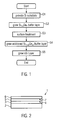
- Fig. 1 is a block diagram illustrating a first embodiment of the inventive method for forming a semiconductor heterostructure.
- a silicon substrate is provided. Silicon substrates are readily available with different sizes and different crystalline surfaces.
- a buffer layer of Si 1-x Ge x is grown, preferably epitaxially, on the silicon substrate.
- the buffer layer can be a graded buffer layer, thus the concentration of the two compounds: silicon and germanium changes over the thickness of the buffer layer.
- the germanium concentration can grow until approximately 20%, thereby the in-plane lattice parameter becomes larger. It should be noted, however, that the final germanium concentration can be freely chosen, for instance 30% or 40%, and could even reach 100%.
- the deposition could be carried out by molecular beam epitaxy.
- Table 2 Si precursor Ge precursor deposition temperature SiH 4 GeH 4 800°C - 900°C SiH 2 Cl 2 GeH 4 800°C - 950°C SiH 2 Cl 2 GeCl 4 1000°C-1100°C SiHCl 3 GeCl 4 1050°C-1150°C
- a strained silicon (sSi) layer is epitaxially deposited on the additional buffer layer using state of the art layer deposition methods.
- a second embodiment of the inventive method for forming a semiconductor heterostructure comprises steps S1 to S3 and S5 of the first embodiment. Their description will not repeated again, but is incorporated herewith by reference.
- the difference with respect to the first embodiment lies in the fact that during the growth of the additional layer (step S4) a growth temperature is used which is lower than the growth temperature used during formation of the buffer layer 3.
- the growth temperature for the additional Si 1-x Ge x layer is chosen to be about 50°C to about 500°C lower than the growth temperature of the graded buffer layer.
Abstract
Description
- The invention relates to a method for forming a semiconductor heterostructure comprising providing a substrate with a first in-plane lattice parameter a1, providing a buffer layer with a second in-plane lattice parameter a2, providing a top layer over the buffer layer. The invention furthermore relates to a corresponding semiconductor heterostructure and to semiconductor devices comprising such a semiconductor heterostructure.
- Semiconductor heterostructures like this are known from
US 5,442,205 disclosing semiconductor heterostructure devices with strained semiconductor layers. The known heterostructure includes a strained epitaxial layer of silicon or germanium which is located over a silicon substrate with a spatially graded GexSi1-x epitaxial layer, which in turn is overlaid by an ungraded capping layer Gex0Si1-x0, intervening between the silicon substrate and the strained layer. The graded layer and the capping layer therein play the role of the buffer layer and the strained layer the role of the top layer. Such heterostructures can serve, for instance, as a foundation for surface emitting LEDs or MOS FETs. - The spatially graded GexSi1-x layer of the buffer layer is used to adapt the lattice parameter between the underlying substrate and the deposited relaxed material, while trying to minimize the density of defects. Usually the additional capping layer of SiGe with constant Ge concentration corresponding to the concentration obtained at the top of the graded layer is provided as a relaxed layer to improve the crystalline quality of the structure.
- The structure obtained usually has a surface morphology which is not suitable for further use.
US2003/0216990 , which is preoccupied by preventing interdiffusion of dopants in semiconductor heterostructures, proposes a planarization step, in particular a Chemical Mechanical Polishing (CMP) step, before growing any further layer, Here it is the role of CMP to provide a polished smooth surface, which is typically of about 2 Å. Following CMP, the substrate needs to be further treated to prepare the subsequent layer deposition. Such treatments include treating the surface using a HF solution and furthermore a bake to remove any oxide. ThenUS2003/0215990 proposes the epitaxial deposition of further layers like silicon germanium or strained silicon layers. - It appears, however, that the achieved surface properties for the semiconductor heterostructures are unsatisfying, when applying the above described prior art processes. Indeed, due to the bake prior to the deposition of the further layers, a roughening of the silicon germanium surface occurs. During the subsequent growth of, e.g., the strained silicon layer, the surface roughness tends to diminish again the final roughness, but nevertheless stays considerably higher than the roughness of the graded GeSi layer surface or of the capping layer, if present, after the CMP process, as the thickness of the strained silicon layer cannot exceed the critical thickness, beyond which defects would nucleate within the layer or at the interface of the strained and the underlying layers, Therefore the overall thickness of the strained silicon layer is too thin, so that no additional CMP can be carried out for flattening out the surface of the strained silicon layer to the desired values. In addition to the thickness aspect allowing a partial improvement of the surface roughness,
US2003/0215990 also proposes to control the temperature at which the layers are grown after planarization, but still only final surface roughness values of the order of 5 Å are achieved. - Furthermore the buried interface between the top layer, e.g. the strained layer, and the underlying layer have even a higher roughness, due to the bake after CMP of the buffer layer. This buried interface can, however, become a top free surface in case the strained layer is transferred onto a handle substrate to create a strained silicon on insulator type semiconductor heterostructure. This can, for example, be achieved using a SmartCut technology based process. Again also here, no additional CMP can be carried out for flattening out the surface.
- The surface roughness is critical for the substrate quality, as a rough surface on the heterostructure will in turn lead to a rough final structure for electronic devices developed thereon and is furthermore detrimental for the electrical behavior of the formed devices. It is therefore the object of the present invention to provide a method for forming a heterostructure and a corresponding semiconductor heterostructure which has better surface roughness properties and/or better buried interface roughness properties.
- This object is achieved with the methods for forming a semiconductor heterostructure according to claims 1.
- It is the surprising finding of this invention that by providing an additional layer, in particular after the planarization and bake steps, between the buffer layer and the top layer, wherein the value of the in-plane lattice parameter of the additional layer is chosen such that it is in between the value of the first and second lattice parameter, the surface roughness of the additional layer is reduced compared to the surface roughness of the underlying buffer layer. As a consequence the surface roughness of the heterostructure is reduced in comparison to the state of the art heterostructures. This is due to the fact that the top layer grows on a already smoother surface. In addition, in the case the top layer gets transferred onto a handle substrate and the buried interface between the additional and the top layer actually becomes the new free surface, also an improved surface roughness will be observed, as the surface of the additional layer is smoother than the surface of the underlying buffer layer.
- In this context the term "in-plane lattice parameter" corresponds to a lattice parameter of the various layers in a direction essentially parallel to the interfaces between the various layers and to lattice parameters which the layers would show in an relaxed state. It is, in fact, known that the lattice parameter depends on the material used, but also on the nature of the underlying material on which it is deposited. To be able to compare lattice parameter values of different layers in the following, it is always referred to values as if the layers were in a relaxed state, and not in the strained state under heteroepitaxial conditions, which is also known under the terms pseudomorphic or commensurate growth. As an interface may be characterized by two lattice parameters, the above-mentioned condition can either be satisfied for both lattice parameters or for only one. Furthermore like mentioned above, the buffer layer can comprise a plurality of layers, e.g. a composition graded layer with or without a capping layer. In the wording of claim 1 the subsequent layer of the substrate is the buffer layer and the subsequent layer of the buffer layer is the additional layer. In addition, the top layer of the heterostructure is not necessarily the final layer, further layers strained or relaxed can be provided thereon.
- According to a preferred embodiment the additional layer and/or the top layer can be grown with a growth temperature lower than the growth temperature of the buffer layer. It is another surprising observation that, in addition to the intermediate in plane lattice parameter of the additional layer, a reducing of the growth temperature for the additional and/or the top layer compared to the growth temperature of the buffer layer, the surface roughness of the semiconductor heterostructure is further improved in comparison to what is achieved according to the prior art. Thus by combining the two roughness reducing methods the overall reduction in surface roughness can be further enhanced.
- Advantageously the growth temperature is chosen to be about 50°C to about 500°C lower than the growth temperature used for forming the buffer layer. The exact choice of the temperature depends e.g. on the precursors used during CVD type deposition of the layers. In this range best results have been achieved for numerous materials.
- According to an advantageous embodiment the thickness of the additional layer can be less than the critical thickness, above which defects occur, in particular less than 1000 Å, more in particular a thickness of about 200 Å to 800 Å, even more in particular of about 600 Å. It should be noted, that the critical thickness depends on the material choice for the additional layer and the underlying layer, but is also a function of deposition temperature. However, for the above mentioned values improved surface roughness values have been obtained. To keep the additional layer thin has the advantage of preventing defects on its surface and furthermore is advantageous with respect to production, as throughput can be kept high.
- Advantageously the buffer layer and the additional layer can comprise at least two compounds A and B and have a different composition A1-xa2Bxa2 and A1-xa3Bxa3 with respect to each other. For example, the buffer layer can be a gradient layer of a binary material, such that starting from the substrate the lattice parameter increases (or diminishes) towards the interface with the top layer and for the additional layer the composition of the binary material can be chosen such that a step back (or increase) in lattice parameter is observed. In fact, by changing the composition usually the lattice parameters change in turn. By using the same compounds, the buffer layer and the additional layer can be grown under similar process conditions and only the supply of the compounds needs to be adapted to realize the different compositions and thus different lattice parameters.
- Preferably the difference in composition Δx = xa2-xa3 is approximately 0.5% to 8%, in particular 2% to 5%, more in particular 2.5%. For those changes in composition, optimized surface roughness values have been achieved for the surface of the top layer. For Δx less than 0.5% the desired flattening effect is not sufficient and for Δx larger than 8% the maximum thickness of the additional layer would be limited to much due to a reduced critical thickness.
- Preferably the top layer can be a strained layer of a relaxed layer, in particular one out of strained silicon (sSi), silicon germanium (Si1-xGex), germanium (Ge) and gallium arsenide (GaAs). These materials are playing an important role in modem electronics and therefore with improved semiconductor heterostructures of these materials optimized electronic properties can be achieved. Advantageously the substrate can be silicon and/or the buffer layer can be silicon germanium (Si1-xa2Gexa2). The silicon as a standard material is readily available and allows to keep fabrication costs low and furthermore with respect to silicon germanium the buffer layer deposition process is well established so that high quality graded layers or layers with a stepped composition can be achieved by playing with the supply of the silicon and germanium precursors respectively. According to a preferred embodiment the additional layer can be silicon germanium (Si1-xa3Gexa3) . Thus to grow the additional layer one only has to adapt the process already used for the buffer layer to grow the desired layer.
- According to a preferred embodiment, starting from a Si substrate, the lattice parameter of the buffer layer increases. The resulting surface roughness after CMP and bake of the buffer layer can be attributed to a surface topology having peaks and valleys, wherein the lattice parameter of the crystalline material tends to be larger on the peak, compared to the nominal lattice parameter, and tends to be smaller in the valleys. By now growing the additional layer with a smaller nominal lattice parameter, the growth speed of the layer in the valleys shall be higher than for the peaks, as a better match of lattice parameters is observed. Thereby leading to the desired surface flattening effect.
- Preferably the growth temperature of silicon germanium when used for the top layer and/or the additional layer can be chosen to be:
Table 1: layer material growth temperature [°C] Si1-xGex, xε[0,20] 650 - 750 Si1-xGex,xε[20,40] 600 - 700 Si1-xGex,xε[40,60] 550 - 650 Si1-xGex,xε[60,80] 500 - 600 Si1-xGex,xε[80,90] < 600 Si1-xGex,xε[90,100] < 550 - Preferably the precursor for the additional layer can be selected such that they do not incorporate an halide element. For GeSi, this would lead for instance to a germane and silane or disilane precursor. The presence of an halide in the precursor creates the risk to have crystalline defects revealed, e.g. due to preferential etching at the location of a crystalline defect, which could be present in a GeSi material, and which would lead to an increase in the size of the defect and deteriorate the quality of the layer.
- The invention also relates to a semiconductor heterostructure according to
claim 12. As explained above such a semiconductor heterostructure benefits from improved surface roughness values. - Semiconductor heterostructure according to
claim 12, wherein the surface roughness of the top layer is less than 1.8 Å RMS, in particular less than 1.5 Å RMS, even more in particular less than 1.3 Å RMS. Such low surface roughness values are advantageous as actually the electrical behavior of devices formed thereon heavily depends on the roughness of the initial substrate. - Semiconductor heterostructure according to claim 12 or 13, wherein the interface roughness at the interface between the additional layer and the top layer is less than 2.5 Å RMS, in particular less than 2.0 Å RMS, even more in particular less than 1.8 Å RMS. Depending on the use of the semiconductor heterostructure the buried interface between the additional layer and the top layer can become a free surface again and in this case an improved surface roughness is advantageous as in particular electronic properties depend heavily on the surface roughness.
- According to a variant, the buffer layer and the additional layer can comprise at least two compounds A and B and have a different composition A1-xa2Bxa2 and A1-xa3Bxa3 with respect to each other. By changing the composition of the layers desired lattice parameters can be easily achieved by changing the growth conditions
- According to a variant, the difference in composition Δx = xa2-xa3 is approximately 0,5 to 8%, in particular 2% to 5%, more in particular 2.5%, as previously stated. For these values optimized surface roughness values have been observed. For Δx less than 0.5% the desired flattening effect is not sufficient and for Δx larger than 8% the maximum thickness of the additional layer would be limited to much due to a reduced critical thickness.
- Preferably the thickness of the additional layer and/or the top layer is less than the critical thickness above which defects occur, in particular less than 1000 Å, more in particular of about 200 Å to 800 Å, even more in particular of about 600 Å. To keep the additional layer thin has the advantage of preventing defects on its surface and furthermore is advantageous with respect to production, as throughput can be kept high. Furthermore the creation of dislocations is prevented. It has been observed that the surface roughness tends to become better after the growth of the top layer material, which would actually incite one to grow thicker layers to provide minimal layer roughness. This advantageous effect of the thickness is, however, limited by the critical thickness as in crystalline structures grown on underlying layers with different crystalline parameters, growing stress leads to defects like dislocations, which in turn deteriorate the quality of the substrate.
- Preferably the top layer can be one out of strained silicon, silicon germanium and germanium and the substrate can be silicon and the buffer layer can be silicon germanium.
- The invention furthermore relates to the use of the semiconductor heterostructure as described above, as a substrate in the fabrication process of the semiconductor devices. With the optimized surface roughness, the electrical behavior of the semiconductor devices fabricated on the semiconductor heterostructure according to the invention will be superior to devices formed on state of the art semiconductor heterostructures.
- The invention furthermore relates to the use of a semiconductor heterostructure as described above as a substrate in the fabrication process of a semiconductor device. In addition the semiconductor heterostructure as disclosed above can advantageously used in the fabrication process of a strained layer on insulator wafer, in particular a strained silicon on insulator wafer. With the improved surface roughness of the inventive semiconductor heterostructure electronic devices with improved properties and engineered substrates with improved properties are achievable. In particular substrates comprising strained layers, like strained silicon, become more and more important they are at the basis of faster semiconductor devices.
- Preferably the semiconductor heterostructure as disclosed above can be used in a SmartCut type fabrication process, wherein the semiconductor heterostructure is used as a donor substrate. Typically a SmartCut type process comprises the steps of providing a handle substrate, e.g. a silicon wafer, forming a predetermined splitting area in a donor substrate, attaching the donor substrate to the handle substrate and detaching the donor substrate at the predetermined splitting area to thereby transfer a layer of the donor substrate onto the handle substrate to create a compound material wafer. By forming the predetermined splitting area in the additional layer or at the buried interface between additional layer and top layer, the buried interface will become the free surface of the compound material wafer following an etching step, to remove remaining material of the additional layer. As the buried interface has improved surface roughness when using a semiconductor heterostructure according to the invention the final quality of the engineered wafer obtained by the SmartCut process is improved, as far as the final etching step is controlled so that it does not deteriorate the final surface roughness.
- The invention also relates to a semiconductor device comprising a semiconductor heterostructure as described above. As mentioned above, the semiconductor device will show superior electrical behavior compared to a similar semiconductor device comprising a state of the art heterostructure substrate.
- The invention also relates to a strained silicon on insulator wafer (sSOI) comprising a wafer, in particular a Si wafer, and on one surface thereof a strained Si layer having been transferred onto the wafer from a semiconductor heterostructure as disclosed above, wherein the top layer is a strained silicon layer and wherein the originally buried interface between the strained silicon layer and the additional layer corresponds to the free surface of the sSOI wafer. This sSOI wafer distinguishes itself from the prior art by the fact that its surface roughness qualities are improved with respect to prior art sSOI wafers.
- Advantageous embodiments of the invention will be described in the following with respect to the figures:
- Fig. 1 illustrates a first embodiment of the inventive method for forming a semiconductor heterostructure,
- Fig. 2 illustrates a corresponding inventive semiconductor heterostructure, and
- Figs. 3a to 3f illustrate a SmartCut type process using the semiconductor heterostructure according to the invention.
- The following embodiments will be described using a silicon substrate, a silicon germanium buffer layer and a strained silicon layer. This does, however, not represent a limitation of the invention to those materials. Indeed, the invention can also be applied to other suitable materials, like strained SiGe, SiGeC, Ge or GaAs.
- Fig. 1 is a block diagram illustrating a first embodiment of the inventive method for forming a semiconductor heterostructure. In step S1 a silicon substrate is provided. Silicon substrates are readily available with different sizes and different crystalline surfaces. Then in step S2 a buffer layer of Si1-xGex is grown, preferably epitaxially, on the silicon substrate. The buffer layer can be a graded buffer layer, thus the concentration of the two compounds: silicon and germanium changes over the thickness of the buffer layer. By doing so the lattice parameter in the graded buffer slowly changes. For example, one can start with x=0 at the interface towards the silicon substrate, so that the lattice parameter corresponds to the one of the underlying Si substrate. Then the germanium concentration can grow until approximately 20%, thereby the in-plane lattice parameter becomes larger. It should be noted, however, that the final germanium concentration can be freely chosen, for instance 30% or 40%, and could even reach 100%.
- The growth of the buffer layer can be achieved using state of the art techniques, for example chemical vapor deposition in an epitaxial equipment using standard process conditions. Suitable precursor gases for the deposition of silicon germanium include for example SiH4, Si3H8, Si2H6, DCS or TCS and GeH4, GeH3Cl, GeH2Cl2, GeHCl3 or GeCl4 together with H2 as a carrier gas. Depending on the precursor gases and their decomposition temperature the deposition temperature is chosen, as can be seen from Table 2, which represents some possible examples suitable for the growth of Si1-xa2Gexa2 with a germanium content of up to about 20%. The composition gradient is achieved by adapting the amount of the Si and/or Ge precursor. Alternatively the deposition could be carried out by molecular beam epitaxy.
Table 2: Si precursor Ge precursor deposition temperature SiH4 GeH4 800°C - 900°C SiH2Cl2 GeH4 800°C - 950°C SiH2Cl2 GeCl4 1000°C-1100°C SiHCl3 GeCl4 1050°C-1150°C - Then in step S3 a surface treatment is carried out which comprises chemical mechanical polishing (CMP) to obtain a surface on the Si1-xa2Gexa2 layer having a roughness of about 1.3 Å RMS, obtained for a scan window of 2µm*2µm. Then the achieved structure undergoes a bake step, e.g. is emerged in hydrofluoric acid HF and heated in hydrogen H2 for about three minutes in a temperature range of about 800 to 850°C. This step is used to remove oxide from the surface of the buffer layer, but the bake step leads to an increased surface roughness of about 2.6 Å RMS.
- Following the surface treatment, in step S4, an additional layer is grown on the buffer layer. This additional layer is grown with a constant composition of the same compounds silicon and germanium, but with a composition Si1-xa3Gexa3 different to the composition of the final layer of the buffer layer. Having the same compounds, essentially the same growth conditions can be chosen, except for the amount of precursor gas provided for each compound. The total thickness of the additional layer and all further layers that are not lattice matched with the buffer layer should be less than the critical thickness, to prevent the nucleation of dislocations or other defects which would occur above this thickness. The value of the critical thickness depends on the difference in Ge concentration between buffer layer and additional layer, and also depends on deposition temperature. Best results have been achieved for thicknesses of less than 1000 Å, in particular for a thickness in a range of about 200 Å to 600 Å, more in particular of about 600 Å for the additional layer. The composition of the second layer is chosen such that the in-plane lattice parameter is smaller than the in-plane lattice parameter of the final layer of the first buffer layer. With the germanium composition of 20% on top of the buffer layer, in this example, suitable percentages for the additional layer are of 12 to 19.5%, in particular 17.5% of germanium. For 40% Ge in the buffer layer, Ge concentration in the additional layer is between 35% and 39.5%.
- Then in step S5 a strained silicon (sSi) layer is epitaxially deposited on the additional buffer layer using state of the art layer deposition methods.
- Fig. 2 illustrates the result obtained after that the inventive process has been carried out as described above. The semiconductor heterostructure 1 according to this embodiment thus comprises a
silicon substrate 2 with a first in-plane lattice parameter a1, a graded Si1-xa2Gexa2 buffer layer 3 having a germanium percentage of 0% at the interface with thesubstrate 2 and having a germanium percentage of about 20% at itsupper surface 4. Within thebuffer layer 3 the in plane lattice parameter a2 increases as the amount of Ge increases. The graded buffer layer is essentially relaxed. On the gradedbuffer layer 3 an additional, epitaxial Si1-xa3Gexa3 layer 5 is provided, which as described above has been formed after CMPing and baking thebuffer layer 3. The additional layer has a germanium percentage which is in a range of about 12 to 19.5%, in particular 17,5%. So that its nominal, thus relaxed, in-plane lattice parameter a3 is less than a2 on top of thebuffer layer 3. However, as the thickness is less than the critical thickness theadditional layer 5 is strained meaning that its in-plane lattice parameter is larger than the nominal value. Finally on top of theadditional layer 5 thestrained silicon layer 6 as top layer is present. - For a
strained silicon layer 6 with a thickness of about 200Å, surface roughness values of less than 1.8 Å RMS, in particular less than 1.3 Å RMS, have been achieved with a post-bake roughness of thebuffer layer 3 being of the order of about 2.6 Å RMS. Up to now, with the state of the art processes, only surface roughnesses exceeding 1.8 Å RMS have been observed. - It should be noted that already the buried
interface 7 between theadditional layer 5 and thestrained silicon layer 6 has already a roughness of less than 2.5 Å RMS, in particular less than 2.0 Å RMS, even more in particular of less than 1.8 Å RMS. The buried interface roughness is thus improved with respect tointerface 4 having a roughness of the order of 2.6 Å after CMP and bake. - The first embodiment of the invention has been explained for a graded
buffer layer 3. However, it is also possible to provide a buffer layer having a different composition structure. - IFor example, a capping layer could be provided on the graded
layer 3 prior to CMP and bake, or the buffer layer could comprise a stack of bi-layers, in particular three to five bi-layers, wherein one bi-layer has a graded composition and the second bi-layer a constant composition. A buffer layer being composed of a plurality of layers with constant germanium composition but with a growing composition from layer to layer represents a further alternative. In addition, it is also possible to provide one or more further additional layers, also called capping or relaxed layers, in between theadditional layer 5 and thefinal layer 6. For example, another SiGe layer may be deposited onto the additional buffer layer with a different SiGe composition. - Instead of a silicon germanium buffer layer, other compound materials may be used to slowly increase the lattice parameter starting from the silicon substrate towards the desired value.
- According to a further variant, a germanium Ge,Si1-yGey or SiGeC layer may be grown as a final layer, instead of the
strained silicon layer 6. - A second embodiment of the inventive method for forming a semiconductor heterostructure comprises steps S1 to S3 and S5 of the first embodiment. Their description will not repeated again, but is incorporated herewith by reference. The difference with respect to the first embodiment lies in the fact that during the growth of the additional layer (step S4) a growth temperature is used which is lower than the growth temperature used during formation of the
buffer layer 3. The growth temperature for the additional Si1-xGex layer is chosen to be about 50°C to about 500°C lower than the growth temperature of the graded buffer layer. During growth of the buffer lower one typically looks for a high deposition temperature to ensure high growth rates but by choosing a lower growth temperature for the additional layer, even though growth speed will lower, it is possible to preferably deposit material in the valleys of the surface of the Si1-xGex buffer layer rather than on the peak. As a consequence a smoothing effect occurs this effect adds to the already advantageous effect of having a smaller in-plane lattice parameter applied in the first embodiment. Thus, a further improved smoothing of the surface ofadditional layer 5 and thus also of thetop layer 6, here the strained Silicon layer, will occur. - Indeed, when the growth temperature is high, the total thermal energy of the arriving atoms is high and the surface energy, which is the energy of the surface on which the atoms are deposited, becomes negligible, so that it cannot have a positive impact on smoothening. If, however, the thermal energy is relatively low, like here, the surface energy can have a positive impact, as by depositing atoms into the valleys, the overall surface becomes smaller and an energy gain is observed. Thus, in this case a smoothing of the surface will occur. If, however, the temperature is too low, the thermal energy will not be sufficient for the arriving atoms to move to the preferred nucleation sites in the valleys to reduce the surface energy.
- The semiconductor heterostructure obtained according to the second embodiment corresponds to the one of the first embodiment as shown in Fig. 2, the description of its features is incorporated herewith by reference. Also the additional variants can be applied to the second embodiment. The only difference is that the surface roughness properties are even better both at the buried
interface 7 and on the surface of thetop layer 6. For astrained silicon layer 6 with a thickness of about 200Å, surface roughness values of less than 1.15 Å RMS has been achieved with a post-bake roughness of thebuffer layer 3 being of the order of about 2.6 Å RMS. Also the buriedInterface 7 between theadditional layer 5 and thestrained silicon layer 6 has improved roughness values of less than 1.8 Å RMS, and as low as 1Å RMS. - The advantageous temperature range actually used depends on the material of the layer, e.g. for a Si1-xGex layer on the Germanium content, the precursor gases used, and the layer thickness. Table 3 illustrates the preferred temperature range for the
additional layer 5 as a function of the Germanium percentage in Si1-xGex.Table 3: layer material typical growth temperature buffer layer 3 [°C] growth temperature additional layer 5 [°C] Si1-xGex, xε[0,20] 800 - 900 650 - 750 Si1-xGex,xε[20,40] 750 - 850 600-700 Si1-xGex,xε[40,60] 700 - 800 550 - 650 Si1-xGex,xε[60,80] 650 - 750 500 - 600 Si1-xGex,xε[80,90] 600 - 700 < 600 Si1-xGex,xε[90,100] 550 - 650 < 550 - For CVD layer deposition of the additional layer the precursors have to be chosen such that they have a decomposition temperature which is lower or at least close to the temperature range indicated in table 3 used are chosen. As a consequence it may occur that the growth of the additional layer 5 a different precursor is used or needs to be used than for the
buffer layer 3. - Figs. 3a to 3f illustrate a third embodiment according to the invention, namely a SmartCut type fabrication process using a semiconductor heterostructure according to the first or second embodiment to fabricate a strained layer on insulator wafer, here a strained silicon on insulator wafer (sSOI).
- Fig. 3a illustrate the semiconductor heterostructure 1 comprising the
strained silicon layer 6 and theadditional layer 5, which has been fabricated according to the first or second embodiment described above. The semiconductor heterostructure is used as an initial donor substrate. On the stainedlayer 6 an isolatinglayer 10 is provided. Thislayer 10 is e.g. achieved by thermally oxidizing thestrained layer 6. The heterostructure 1 together with the isolatinglayer 10 builds up adonor substrate 12. - Fig. 3b illustrates a
handle substrate 14, typically a standard wafer, e.g. a Si wafer. The surface of the handle substrate can either be with or without the native or a grown isolating layer, e.g. the native SiO2 layer the case of a Si wafer. - Fig. 3c illustrates the process to create a predetermined splitting area 16 in the initial donor substrate 1. This is achieved by implanting
atomic species 18, like for example hydrogen ions or other inert gases, with a predetermined dose and energy. Due to the implantation the predetermined splitting area 16 is created inside thedonor substrate 12. The implantation conditions are chosen such that the predetermined splitting area 16 is positioned in theadditional layer 5 or close to the buriedinterface 7 towards thetop layer 6. - Fig. 3d illustrates the next step in the process which consists in attaching the
initial donor substrate 12 to thehandle substrate 14 by bonding the free surface of the insulatinglayer 10 of thedonor substrate 12 onto thehandle substrate 14 to thereby form a donor-handle compound 20. Prior to bonding eventually a surface preparation step is carried out. - The donor-handle compound 20 is then placed into a furnace (not shown) and heated such that the predetermined splitting area 16 is fragilized which finally leads to a detachment of the
remainder 22 of thedonor substrate 12. Instead of providing thermal energy, the fragilization and detachment may also be achieved by providing additional energy in any form, for instance mechanical energy or a combination of thermal and mechanical energy. - Fig. 3e illustrates the result of the detachment step. A
compound material wafer 24 is achieved comprising the insulatinglayer 10, thetop layer 6 and a part of theadditional layer 5 in this order on thehandle substrate 14. - The
compound material wafer 24 then undergoes a further surface treatment to remove the remaining part of theadditional layer 5. This can for example be achieved by an etching step. As a consequence the buriedinterface 7 of the original semiconductor heterostructure 1 now becomes the free surface. The final strained silicon oninsulator substrate 26 is illustrated in Fig. 3f. It comprises thehandle substrate 14, the isolatinglayer 10 and thetop layer 6, thus the strained silicon layer. As due to the provision of theadditional layer 5 the buriedinterface 7, now being the free surface, has superior surface roughness properties, the strained silicon wafer according to this embodiment is improved compared to the prior art. Instead of a strained silicon on insulator wafer also other types oftop layers 6 could be transferred including the above mentioned SiGe, Ge or GaAs. - In addition to the sSOI wafer, a SiGe on inulator (SiGeOI) wafer could be produced, for instance by using SiGe as
top layer 6, like mentioned above, or by depositing a relaxed layer of SiGe on thetop layer 6, thus a layer which is lattice matched with the buffer layer. - The semiconductor heterostructures according to the first and second embodiment as well as the strained layer on insulator wafers according to the third embodiment are advantageously used in semiconductor devices, as improved electrical or optical properties can be achieved with the substrates having improved surface roughness properties.
Claims (23)
- Method for forming a semiconductor heterostructure comprising:- providing a substrate (2) with a first in-plane lattice parameter a1,- providing a buffer layer (3) with a second in-plane lattice parameter a2,- providing a top layer (6) over the buffer layer (3)characterized in that
an additional layer (5) is provided in between the buffer layer (3) and the top layer (6), said additional layer (5) having a third in-plane lattice parameter a3 which is in between the first and second lattice parameter a1, a2 to thereby improve the surface roughness of the top layer (6), and wherein the lattice parameters of the substrate and the buffer layer correspond to lattice parameter values in a relaxed state respectively and are the lattice parameters at the interface towards the subsequent layer. - Method according to claim 1, wherein the additional layer (5) and/or the top layer (6) is grown with a growth temperature lower than the growth temperature of the buffer layer (3).
- Method according to claim 2, wherein the growth temperature of the additional layer (5) and/or the top layer (6) is chosen to be about 50°C to about 500°C lower than the growth temperature of the buffer layer (3).
- Method according to claim 1 to 3, wherein the thickness of the additional layer (5) is less than the critical thickness above which defects occur, in particular less than 1000 Å, more in particular a thickness of about 200 Å to 800 Å, even more in particular of about 600 Å.
- Method according to one of claims 1 to 4, wherein the buffer layer (3, 13) and the additional layer (5) are comprising at least two compounds A and B and have a different composition A1-xa2Bxa2 and A1-xa3Bxa3 with respect to each other.
- Method according to claim 5, wherein the difference in composition Δx = xa2-xa3 is approximately 0.5% to 8%, in particular 2% - 5%, more in particular 2.5%.
- Method according to one of claims 1 to 6, wherein the top layer (6) is a strained layer or a relaxed layer, in particular one out of silicon (sSi), silicon germanium (Si1-xGex) and germanium (Ge).
- Method according to one of claims 1 to 7, wherein the substrate (12) is silicon and/or the buffer layer (3, 13) is silicon germanium (Si1-xa2Gexa2).
- Method according to one of claims 1 to 8,wherein the additional layer (5) is silicon germanium (Si1-xa3Gexa3).
- Method according to one of claims 7 to 9, wherein the growth temperature of silicon germanium (Si1-xGex) when used for the top layer (6) and/or the additional layer (5) is according depending on the germanium percentage:
layer material growth temperature [°C] Si1-xGex,xε[0,20] 650 - 750 Si1-xGex,xε[20,40] 600 - 700 Si1-xGex,xε[40,60] 550 - 650 Si1-xGex,xε[60,80] 500 - 600 Si1-xGex,xε[80,90] < 600 Si1-xGex,xε[90,100] < 550 - Method according to one of claims 6 to 10, wherein the growth temperature of silicon when used for the top layer (6), is chosen to be less than 600°C, in particular less than 550°C to 700°C, or wherein the growth temperature of germanium when used for the top layer (6), is chosen to be less than 500°C.
- Semiconductor heterostructure comprising:- a substrate (2) with a first in-plane lattice parameter a1,- a buffer layer (3) with a second in-plane lattice parameter a2,- a top layer (6) over the buffer layer (3)characterized in that
an additional layer (5) is in between the buffer layer (3) and the top layer (6), said additional layer (5) having a third in-plane lattice parameter a3 which is in between the first and second lattice parameter, wherein the lattice parameters of the layers correspond to lattice parameter values in a relaxed state respectively and are the lattice parameters at the interface towards the subsequent layer. - Semiconductor heterostructure according to claim 12, wherein the surface roughness of the top layer (6) is less than 1.8 Å RMS, in particular less than 1.5 Å RMS, even more in particular less than 1.3 Å RMS.
- Semiconductor heterostructure according to claim 12 or 13, wherein the interface roughness at the interface between the additional layer (5) and the top layer (6) is less than 2.5 Å RMS, in particular less than 2.0 Å RMS, even more in particular less than 1.8 Å RMS.
- Semiconductor heterostructure according to one of claims 12 to 14, wherein the buffer layer (3) and the additional layer (5) are comprising at least two compounds A and B and have a different composition A1-xa2Bxa2 and A1-xa3Bxa3 with respect to each other.
- Semiconductor heterostructure according to claim 15, wherein the difference in composition Δx = xa2-xa3 is approximately 0,5% to 8%, in particular 2% to 5%, more in particular 2.5%.
- Semiconductor heterostructure according to one of claims 12 to 16, wherein the thickness of the additional layer (5) and/or the top layer is less than the critical thickness above which defects occur, in particular less than 1000 Å, more in particular a thickness of about 200 Å to 800 Å, even more in particular of about 600 Å.
- Semiconductor heterostructure according to one of claims 12 to 17, wherein the substrate (2, 12) is silicon and/or the buffer layer (3, 13) is silicon germanium (Si1-xa2Gexa2) and/or the top layer (5) is a strained layer or a relaxed layer, in particular one out of strained silicon (sSi), silicon germanium (Si1-xGex) and germanium (Ge), and/or the additional layer is silicon germanium (Si1-xa3Gexa3).
- Use of a semiconductor heterostructure according to one of claims 12 to 18, as a substrate in the fabrication process of a semiconductor device.
- Use of a semiconductor heterostructure according to one of claims 12 to 18 in the fabrication process of a strained layer on insulator wafer, in particular a strained silicon on insulator wafer.
- Use of a semiconductor heterostructure according to claim 19, wherein the fabrication process is a SmartCut type process and the semiconductor heterostructure according to one of claims 12 to 18 is used as a donor substrate.
- Semiconductor device comprising a semiconductor heterostructure according to one of claims 12 to 18.
- Strained silicon on insulator wafer (sSOI) comprising a wafer, in particular a Si wafer, and on one surface thereof a strained Si layer having been transferred onto the wafer from a semiconductor heterostructure according to one of claims 12 to 18, wherein the top layer (6) is a strained silicon layer and wherein the originally buried interface (7) between the strained silicon layer (6) and the additional layer (5) corresponds to the free surface of the sSOI wafer.
Priority Applications (9)
| Application Number | Priority Date | Filing Date | Title |
|---|---|---|---|
| EP05291841.4A EP1763069B1 (en) | 2005-09-07 | 2005-09-07 | Method for forming a semiconductor heterostructure |
| US11/267,494 US7772127B2 (en) | 2005-09-07 | 2005-11-03 | Semiconductor heterostructure and method for forming same |
| TW095128555A TWI343650B (en) | 2005-09-07 | 2006-08-03 | Semiconductor heterostructure and method for forming a semiconductor heterostructure |
| JP2006218649A JP4907256B2 (en) | 2005-09-07 | 2006-08-10 | Semiconductor heterostructure and method for forming a semiconductor heterostructure |
| SG200605904-2A SG131023A1 (en) | 2005-09-07 | 2006-08-29 | Semiconductor heterostructure and method for forming a semiconductor heterostructure |
| SG200901502-5A SG150571A1 (en) | 2005-09-07 | 2006-08-29 | Semiconductor heterostructure and method for forming a semiconductor heterostructure |
| KR1020060084767A KR100832152B1 (en) | 2005-09-07 | 2006-09-04 | semiconductor heterostructure, method for forming the semiconductor heterostructure and strained silicon on insulataor wafersSOI comprising the semiconductor heterostructure |
| CN2006101289688A CN101140864B (en) | 2005-09-07 | 2006-09-05 | Semiconductor heterostructure and method for forming a semiconductor heterostructure |
| US12/827,135 US8084784B2 (en) | 2005-09-07 | 2010-06-30 | Semiconductor heterostructure and method for forming same |
Applications Claiming Priority (1)
| Application Number | Priority Date | Filing Date | Title |
|---|---|---|---|
| EP05291841.4A EP1763069B1 (en) | 2005-09-07 | 2005-09-07 | Method for forming a semiconductor heterostructure |
Publications (2)
| Publication Number | Publication Date |
|---|---|
| EP1763069A1 true EP1763069A1 (en) | 2007-03-14 |
| EP1763069B1 EP1763069B1 (en) | 2016-04-13 |
Family
ID=35130550
Family Applications (1)
| Application Number | Title | Priority Date | Filing Date |
|---|---|---|---|
| EP05291841.4A Active EP1763069B1 (en) | 2005-09-07 | 2005-09-07 | Method for forming a semiconductor heterostructure |
Country Status (7)
| Country | Link |
|---|---|
| US (2) | US7772127B2 (en) |
| EP (1) | EP1763069B1 (en) |
| JP (1) | JP4907256B2 (en) |
| KR (1) | KR100832152B1 (en) |
| CN (1) | CN101140864B (en) |
| SG (2) | SG150571A1 (en) |
| TW (1) | TWI343650B (en) |
Cited By (4)
| Publication number | Priority date | Publication date | Assignee | Title |
|---|---|---|---|---|
| GB2467935A (en) * | 2009-02-19 | 2010-08-25 | Iqe Silicon Compounds Ltd | A method of forming a film of GaAs and germanium materials |
| WO2011082079A1 (en) * | 2009-12-30 | 2011-07-07 | Memc Electronic Materials, Inc. | Method for the preparation of a multi-layered crystalline structure |
| KR20190098308A (en) * | 2018-02-13 | 2019-08-22 | 삼성디스플레이 주식회사 | Method for fabricating thin film transistor substrate |
| JP2021527954A (en) * | 2018-06-21 | 2021-10-14 | ソイテックSoitec | Front image sensor and method for manufacturing such an image sensor |
Families Citing this family (21)
| Publication number | Priority date | Publication date | Assignee | Title |
|---|---|---|---|---|
| US7785995B2 (en) * | 2006-05-09 | 2010-08-31 | Asm America, Inc. | Semiconductor buffer structures |
| JP5380794B2 (en) * | 2007-06-22 | 2014-01-08 | 富士通セミコンダクター株式会社 | Method for manufacturing semiconductor device and method for forming semiconductor layer |
| FR2918793B1 (en) * | 2007-07-11 | 2009-10-09 | Commissariat Energie Atomique | PROCESS FOR PRODUCING A SEMICONDUCTOR-SUR-INSULATING SUBSTRATE FOR MICROELECTRONICS AND OPTOELECTRONICS |
| KR100873299B1 (en) * | 2007-08-20 | 2008-12-11 | 주식회사 실트론 | Manufacturing method for ssoi wafer |
| US7791063B2 (en) * | 2007-08-30 | 2010-09-07 | Intel Corporation | High hole mobility p-channel Ge transistor structure on Si substrate |
| CN102315246B (en) * | 2010-06-30 | 2013-03-13 | 中国科学院上海硅酸盐研究所 | Relaxation SiGe virtual substrate and preparation method thereof |
| CN102122636B (en) * | 2010-12-08 | 2013-06-19 | 中国科学院上海微系统与信息技术研究所 | Preparation method of three-dimensional resistance conversion memory chip |
| FR2972567B1 (en) * | 2011-03-09 | 2013-03-22 | Soitec Silicon On Insulator | METHOD OF FORMING A STRUCTURE OF GE ON III / V ON INSULATION |
| CN102738327A (en) * | 2011-04-13 | 2012-10-17 | 展晶科技(深圳)有限公司 | Semiconductor epitaxial structure and manufacturing method thereof |
| FR2977260B1 (en) | 2011-06-30 | 2013-07-19 | Soitec Silicon On Insulator | PROCESS FOR PRODUCING A THICK EPITAXIAL LAYER OF GALLIUM NITRIDE ON A SILICON SUBSTRATE OR THE LIKE AND LAYER OBTAINED BY SAID METHOD |
| US9127345B2 (en) | 2012-03-06 | 2015-09-08 | Asm America, Inc. | Methods for depositing an epitaxial silicon germanium layer having a germanium to silicon ratio greater than 1:1 using silylgermane and a diluent |
| US9171715B2 (en) | 2012-09-05 | 2015-10-27 | Asm Ip Holding B.V. | Atomic layer deposition of GeO2 |
| FR2995447B1 (en) | 2012-09-07 | 2014-09-05 | Soitec Silicon On Insulator | METHOD FOR SEPARATING AT LEAST TWO SUBSTRATES ACCORDING TO A CHOSEN INTERFACE |
| US9583364B2 (en) * | 2012-12-31 | 2017-02-28 | Sunedison Semiconductor Limited (Uen201334164H) | Processes and apparatus for preparing heterostructures with reduced strain by radial compression |
| US9218963B2 (en) | 2013-12-19 | 2015-12-22 | Asm Ip Holding B.V. | Cyclical deposition of germanium |
| US9611133B2 (en) * | 2014-09-11 | 2017-04-04 | Invensense, Inc. | Film induced interface roughening and method of producing the same |
| US9490123B2 (en) * | 2014-10-24 | 2016-11-08 | Globalfoundries Inc. | Methods of forming strained epitaxial semiconductor material(S) above a strain-relaxed buffer layer |
| US10923344B2 (en) * | 2017-10-30 | 2021-02-16 | Asm Ip Holding B.V. | Methods for forming a semiconductor structure and related semiconductor structures |
| US10355105B2 (en) | 2017-10-31 | 2019-07-16 | Taiwan Semiconductor Manufacturing Company, Ltd. | Fin field-effect transistors and methods of forming the same |
| US20220389560A1 (en) * | 2019-11-07 | 2022-12-08 | Oerikon Surface Solutions AG, Pfäffikon | Method for Producing a Coating |
| CN112927758A (en) * | 2019-12-05 | 2021-06-08 | 有研工程技术研究院有限公司 | Rapid and effective heterogeneous interface modeling method |
Citations (6)
| Publication number | Priority date | Publication date | Assignee | Title |
|---|---|---|---|---|
| US5442205A (en) | 1991-04-24 | 1995-08-15 | At&T Corp. | Semiconductor heterostructure devices with strained semiconductor layers |
| US20030203600A1 (en) * | 2002-02-11 | 2003-10-30 | International Business Machines Corporation | Strained Si based layer made by UHV-CVD, and devices therein |
| US20030215990A1 (en) | 2002-03-14 | 2003-11-20 | Eugene Fitzgerald | Methods for fabricating strained layers on semiconductor substrates |
| EP1439570A1 (en) * | 2003-01-14 | 2004-07-21 | Interuniversitair Microelektronica Centrum ( Imec) | SiGe strain relaxed buffer for high mobility devices and a method of fabricating it |
| EP1447839A1 (en) * | 2001-08-06 | 2004-08-18 | Sumitomo Mitsubishi Silicon Corporation | SEMICONDUCTOR SUBSTRATE, FIELD−EFFCT TRANSISTOR, AND THEIR MANUFACTURING METHODS |
| US20050179028A1 (en) * | 2004-02-17 | 2005-08-18 | Pang-Shiu Chen | Construction of thin strain-relaxed SiGe layers and method for fabricating the same |
Family Cites Families (18)
| Publication number | Priority date | Publication date | Assignee | Title |
|---|---|---|---|---|
| JPH08264552A (en) * | 1995-03-24 | 1996-10-11 | Toshiba Ceramics Co Ltd | Production of silicon wafer |
| US6154475A (en) * | 1997-12-04 | 2000-11-28 | The United States Of America As Represented By The Secretary Of The Air Force | Silicon-based strain-symmetrized GE-SI quantum lasers |
| US6350993B1 (en) * | 1999-03-12 | 2002-02-26 | International Business Machines Corporation | High speed composite p-channel Si/SiGe heterostructure for field effect devices |
| JP3393602B2 (en) * | 2000-01-13 | 2003-04-07 | 松下電器産業株式会社 | Semiconductor device |
| JP3985519B2 (en) * | 2001-12-27 | 2007-10-03 | 株式会社Sumco | Semiconductor substrate, field effect transistor, and manufacturing method thereof |
| US6562703B1 (en) * | 2002-03-13 | 2003-05-13 | Sharp Laboratories Of America, Inc. | Molecular hydrogen implantation method for forming a relaxed silicon germanium layer with high germanium content |
| JP3719998B2 (en) | 2002-04-01 | 2005-11-24 | 松下電器産業株式会社 | Manufacturing method of semiconductor device |
| KR100460201B1 (en) * | 2002-04-08 | 2004-12-08 | 한국전자통신연구원 | Manufacturing method of a virtual substrate for SiGe/Si hetero-junction field-effect transistor |
| JP2003347229A (en) * | 2002-05-31 | 2003-12-05 | Renesas Technology Corp | Method of manufacturing semiconductor device and semiconductor device |
| US6995430B2 (en) * | 2002-06-07 | 2006-02-07 | Amberwave Systems Corporation | Strained-semiconductor-on-insulator device structures |
| AU2003274922A1 (en) * | 2002-08-23 | 2004-03-11 | Amberwave Systems Corporation | Semiconductor heterostructures having reduced dislocation pile-ups and related methods |
| KR100605504B1 (en) * | 2003-07-30 | 2006-07-28 | 삼성전자주식회사 | semiconductor device comprising epitaxial layer with low dislocation density and fabricating method of the semiconductor device |
| EP1709671B1 (en) * | 2004-01-16 | 2012-04-04 | International Business Machines Corporation | Method of forming thin sgoi wafers with high relaxation and low stacking fault defect density |
| US6995078B2 (en) * | 2004-01-23 | 2006-02-07 | Chartered Semiconductor Manufacturing Ltd. | Method of forming a relaxed semiconductor buffer layer on a substrate with a large lattice mismatch |
| WO2005119762A1 (en) * | 2004-05-27 | 2005-12-15 | Massachusetts Institute Of Technology | Single metal gate material cmos using strained si-silicon germanium heterojunction layered substrate |
| US20060151787A1 (en) * | 2005-01-12 | 2006-07-13 | International Business Machines Corporation | LOW CONCENTRATION SiGe BUFFER DURING STRAINED Si GROWTH OF SSGOI MATERIAL FOR DOPANT DIFFUSION CONTROL AND DEFECT REDUCTION |
| EP1705697A1 (en) * | 2005-03-21 | 2006-09-27 | S.O.I. Tec Silicon on Insulator Technologies S.A. | Composition graded layer structure and method for forming the same |
| EP1933384B1 (en) * | 2006-12-15 | 2013-02-13 | Soitec | Semiconductor heterostructure |
-
2005
- 2005-09-07 EP EP05291841.4A patent/EP1763069B1/en active Active
- 2005-11-03 US US11/267,494 patent/US7772127B2/en active Active
-
2006
- 2006-08-03 TW TW095128555A patent/TWI343650B/en active
- 2006-08-10 JP JP2006218649A patent/JP4907256B2/en active Active
- 2006-08-29 SG SG200901502-5A patent/SG150571A1/en unknown
- 2006-08-29 SG SG200605904-2A patent/SG131023A1/en unknown
- 2006-09-04 KR KR1020060084767A patent/KR100832152B1/en active IP Right Grant
- 2006-09-05 CN CN2006101289688A patent/CN101140864B/en active Active
-
2010
- 2010-06-30 US US12/827,135 patent/US8084784B2/en active Active
Patent Citations (6)
| Publication number | Priority date | Publication date | Assignee | Title |
|---|---|---|---|---|
| US5442205A (en) | 1991-04-24 | 1995-08-15 | At&T Corp. | Semiconductor heterostructure devices with strained semiconductor layers |
| EP1447839A1 (en) * | 2001-08-06 | 2004-08-18 | Sumitomo Mitsubishi Silicon Corporation | SEMICONDUCTOR SUBSTRATE, FIELD−EFFCT TRANSISTOR, AND THEIR MANUFACTURING METHODS |
| US20030203600A1 (en) * | 2002-02-11 | 2003-10-30 | International Business Machines Corporation | Strained Si based layer made by UHV-CVD, and devices therein |
| US20030215990A1 (en) | 2002-03-14 | 2003-11-20 | Eugene Fitzgerald | Methods for fabricating strained layers on semiconductor substrates |
| EP1439570A1 (en) * | 2003-01-14 | 2004-07-21 | Interuniversitair Microelektronica Centrum ( Imec) | SiGe strain relaxed buffer for high mobility devices and a method of fabricating it |
| US20050179028A1 (en) * | 2004-02-17 | 2005-08-18 | Pang-Shiu Chen | Construction of thin strain-relaxed SiGe layers and method for fabricating the same |
Cited By (7)
| Publication number | Priority date | Publication date | Assignee | Title |
|---|---|---|---|---|
| GB2467935A (en) * | 2009-02-19 | 2010-08-25 | Iqe Silicon Compounds Ltd | A method of forming a film of GaAs and germanium materials |
| GB2467935B (en) * | 2009-02-19 | 2013-10-30 | Iqe Silicon Compounds Ltd | Formation of thin layers of GaAs and germanium materials |
| US9048289B2 (en) | 2009-02-19 | 2015-06-02 | Iqe Silicon Compounds Limited | Formation of thin layers of semiconductor materials |
| WO2011082079A1 (en) * | 2009-12-30 | 2011-07-07 | Memc Electronic Materials, Inc. | Method for the preparation of a multi-layered crystalline structure |
| US8367519B2 (en) | 2009-12-30 | 2013-02-05 | Memc Electronic Materials, Inc. | Method for the preparation of a multi-layered crystalline structure |
| KR20190098308A (en) * | 2018-02-13 | 2019-08-22 | 삼성디스플레이 주식회사 | Method for fabricating thin film transistor substrate |
| JP2021527954A (en) * | 2018-06-21 | 2021-10-14 | ソイテックSoitec | Front image sensor and method for manufacturing such an image sensor |
Also Published As
| Publication number | Publication date |
|---|---|
| CN101140864B (en) | 2011-03-02 |
| KR100832152B1 (en) | 2008-05-27 |
| TW200735348A (en) | 2007-09-16 |
| JP2007096274A (en) | 2007-04-12 |
| CN101140864A (en) | 2008-03-12 |
| TWI343650B (en) | 2011-06-11 |
| SG131023A1 (en) | 2007-04-26 |
| EP1763069B1 (en) | 2016-04-13 |
| US7772127B2 (en) | 2010-08-10 |
| US8084784B2 (en) | 2011-12-27 |
| SG150571A1 (en) | 2009-03-30 |
| JP4907256B2 (en) | 2012-03-28 |
| US20070051975A1 (en) | 2007-03-08 |
| KR20070028234A (en) | 2007-03-12 |
| US20100264463A1 (en) | 2010-10-21 |
Similar Documents
| Publication | Publication Date | Title |
|---|---|---|
| EP1763069B1 (en) | Method for forming a semiconductor heterostructure | |
| US7459374B2 (en) | Method of manufacturing a semiconductor heterostructure | |
| EP1933384B1 (en) | Semiconductor heterostructure | |
| EP1482549B1 (en) | Method of fabrication of a heteroepitaxial microstructure | |
| EP1709671B1 (en) | Method of forming thin sgoi wafers with high relaxation and low stacking fault defect density | |
| US6927147B2 (en) | Coplanar integration of lattice-mismatched semiconductor with silicon via wafer bonding virtual substrates | |
| JP2008141206A6 (en) | Method for fabricating a semiconductor heterostructure | |
| EP1509949B1 (en) | Formation of lattice-tuning semiconductor substrates | |
| JP6737983B2 (en) | Amorphous SiO2 intermediate layer that relieves stress | |
| US20070134901A1 (en) | Growth of GaAs expitaxial layers on Si substrate by using a novel GeSi buffer layer | |
| KR100611108B1 (en) | Method of manufacturing a thin film layer |
Legal Events
| Date | Code | Title | Description |
|---|---|---|---|
| PUAI | Public reference made under article 153(3) epc to a published international application that has entered the european phase |
Free format text: ORIGINAL CODE: 0009012 |
|
| 17P | Request for examination filed |
Effective date: 20060921 |
|
| AK | Designated contracting states |
Kind code of ref document: A1 Designated state(s): AT BE BG CH CY CZ DE DK EE ES FI FR GB GR HU IE IS IT LI LT LU LV MC NL PL PT RO SE SI SK TR |
|
| AX | Request for extension of the european patent |
Extension state: AL BA HR MK YU |
|
| RIN1 | Information on inventor provided before grant (corrected) |
Inventor name: FIGUET, CHRISTOPHE Inventor name: KENNARD |
|
| AKX | Designation fees paid |
Designated state(s): AT BE BG CH CY CZ DE DK EE ES FI FR GB GR HU IE IS IT LI LT LU LV MC NL PL PT RO SE SI SK TR |
|
| 17Q | First examination report despatched |
Effective date: 20090612 |
|
| RAP1 | Party data changed (applicant data changed or rights of an application transferred) |
Owner name: SOITEC |
|
| GRAP | Despatch of communication of intention to grant a patent |
Free format text: ORIGINAL CODE: EPIDOSNIGR1 |
|
| INTG | Intention to grant announced |
Effective date: 20151120 |
|
| RIN1 | Information on inventor provided before grant (corrected) |
Inventor name: FIGUET, CHRISTOPHE Inventor name: KENNARD, MARK |
|
| GRAS | Grant fee paid |
Free format text: ORIGINAL CODE: EPIDOSNIGR3 |
|
| GRAA | (expected) grant |
Free format text: ORIGINAL CODE: 0009210 |
|
| AK | Designated contracting states |
Kind code of ref document: B1 Designated state(s): AT BE BG CH CY CZ DE DK EE ES FI FR GB GR HU IE IS IT LI LT LU LV MC NL PL PT RO SE SI SK TR |
|
| REG | Reference to a national code |
Ref country code: GB Ref legal event code: FG4D |
|
| REG | Reference to a national code |
Ref country code: AT Ref legal event code: REF Ref document number: 790955 Country of ref document: AT Kind code of ref document: T Effective date: 20160415 Ref country code: CH Ref legal event code: EP |
|
| REG | Reference to a national code |
Ref country code: IE Ref legal event code: FG4D |
|
| REG | Reference to a national code |
Ref country code: DE Ref legal event code: R096 Ref document number: 602005048944 Country of ref document: DE |
|
| REG | Reference to a national code |
Ref country code: LT Ref legal event code: MG4D |
|
| REG | Reference to a national code |
Ref country code: FR Ref legal event code: PLFP Year of fee payment: 12 |
|
| REG | Reference to a national code |
Ref country code: AT Ref legal event code: MK05 Ref document number: 790955 Country of ref document: AT Kind code of ref document: T Effective date: 20160413 |
|
| REG | Reference to a national code |
Ref country code: NL Ref legal event code: MP Effective date: 20160413 |
|
| PG25 | Lapsed in a contracting state [announced via postgrant information from national office to epo] |
Ref country code: PL Free format text: LAPSE BECAUSE OF FAILURE TO SUBMIT A TRANSLATION OF THE DESCRIPTION OR TO PAY THE FEE WITHIN THE PRESCRIBED TIME-LIMIT Effective date: 20160413 Ref country code: NL Free format text: LAPSE BECAUSE OF FAILURE TO SUBMIT A TRANSLATION OF THE DESCRIPTION OR TO PAY THE FEE WITHIN THE PRESCRIBED TIME-LIMIT Effective date: 20160413 Ref country code: LT Free format text: LAPSE BECAUSE OF FAILURE TO SUBMIT A TRANSLATION OF THE DESCRIPTION OR TO PAY THE FEE WITHIN THE PRESCRIBED TIME-LIMIT Effective date: 20160413 Ref country code: FI Free format text: LAPSE BECAUSE OF FAILURE TO SUBMIT A TRANSLATION OF THE DESCRIPTION OR TO PAY THE FEE WITHIN THE PRESCRIBED TIME-LIMIT Effective date: 20160413 |
|
| PG25 | Lapsed in a contracting state [announced via postgrant information from national office to epo] |
Ref country code: SE Free format text: LAPSE BECAUSE OF FAILURE TO SUBMIT A TRANSLATION OF THE DESCRIPTION OR TO PAY THE FEE WITHIN THE PRESCRIBED TIME-LIMIT Effective date: 20160413 Ref country code: PT Free format text: LAPSE BECAUSE OF FAILURE TO SUBMIT A TRANSLATION OF THE DESCRIPTION OR TO PAY THE FEE WITHIN THE PRESCRIBED TIME-LIMIT Effective date: 20160816 Ref country code: AT Free format text: LAPSE BECAUSE OF FAILURE TO SUBMIT A TRANSLATION OF THE DESCRIPTION OR TO PAY THE FEE WITHIN THE PRESCRIBED TIME-LIMIT Effective date: 20160413 Ref country code: LV Free format text: LAPSE BECAUSE OF FAILURE TO SUBMIT A TRANSLATION OF THE DESCRIPTION OR TO PAY THE FEE WITHIN THE PRESCRIBED TIME-LIMIT Effective date: 20160413 Ref country code: GR Free format text: LAPSE BECAUSE OF FAILURE TO SUBMIT A TRANSLATION OF THE DESCRIPTION OR TO PAY THE FEE WITHIN THE PRESCRIBED TIME-LIMIT Effective date: 20160714 Ref country code: ES Free format text: LAPSE BECAUSE OF FAILURE TO SUBMIT A TRANSLATION OF THE DESCRIPTION OR TO PAY THE FEE WITHIN THE PRESCRIBED TIME-LIMIT Effective date: 20160413 |
|
| PG25 | Lapsed in a contracting state [announced via postgrant information from national office to epo] |
Ref country code: BE Free format text: LAPSE BECAUSE OF FAILURE TO SUBMIT A TRANSLATION OF THE DESCRIPTION OR TO PAY THE FEE WITHIN THE PRESCRIBED TIME-LIMIT Effective date: 20160413 Ref country code: IT Free format text: LAPSE BECAUSE OF FAILURE TO SUBMIT A TRANSLATION OF THE DESCRIPTION OR TO PAY THE FEE WITHIN THE PRESCRIBED TIME-LIMIT Effective date: 20160413 |
|
| REG | Reference to a national code |
Ref country code: DE Ref legal event code: R097 Ref document number: 602005048944 Country of ref document: DE |
|
| PG25 | Lapsed in a contracting state [announced via postgrant information from national office to epo] |
Ref country code: EE Free format text: LAPSE BECAUSE OF FAILURE TO SUBMIT A TRANSLATION OF THE DESCRIPTION OR TO PAY THE FEE WITHIN THE PRESCRIBED TIME-LIMIT Effective date: 20160413 Ref country code: SK Free format text: LAPSE BECAUSE OF FAILURE TO SUBMIT A TRANSLATION OF THE DESCRIPTION OR TO PAY THE FEE WITHIN THE PRESCRIBED TIME-LIMIT Effective date: 20160413 Ref country code: CZ Free format text: LAPSE BECAUSE OF FAILURE TO SUBMIT A TRANSLATION OF THE DESCRIPTION OR TO PAY THE FEE WITHIN THE PRESCRIBED TIME-LIMIT Effective date: 20160413 Ref country code: DK Free format text: LAPSE BECAUSE OF FAILURE TO SUBMIT A TRANSLATION OF THE DESCRIPTION OR TO PAY THE FEE WITHIN THE PRESCRIBED TIME-LIMIT Effective date: 20160413 Ref country code: RO Free format text: LAPSE BECAUSE OF FAILURE TO SUBMIT A TRANSLATION OF THE DESCRIPTION OR TO PAY THE FEE WITHIN THE PRESCRIBED TIME-LIMIT Effective date: 20160413 |
|
| PLBE | No opposition filed within time limit |
Free format text: ORIGINAL CODE: 0009261 |
|
| STAA | Information on the status of an ep patent application or granted ep patent |
Free format text: STATUS: NO OPPOSITION FILED WITHIN TIME LIMIT |
|
| 26N | No opposition filed |
Effective date: 20170116 |
|
| PG25 | Lapsed in a contracting state [announced via postgrant information from national office to epo] |
Ref country code: MC Free format text: LAPSE BECAUSE OF FAILURE TO SUBMIT A TRANSLATION OF THE DESCRIPTION OR TO PAY THE FEE WITHIN THE PRESCRIBED TIME-LIMIT Effective date: 20160413 |
|
| REG | Reference to a national code |
Ref country code: CH Ref legal event code: PL |
|
| GBPC | Gb: european patent ceased through non-payment of renewal fee |
Effective date: 20160907 |
|
| PG25 | Lapsed in a contracting state [announced via postgrant information from national office to epo] |
Ref country code: SI Free format text: LAPSE BECAUSE OF FAILURE TO SUBMIT A TRANSLATION OF THE DESCRIPTION OR TO PAY THE FEE WITHIN THE PRESCRIBED TIME-LIMIT Effective date: 20160413 |
|
| REG | Reference to a national code |
Ref country code: IE Ref legal event code: MM4A |
|
| PG25 | Lapsed in a contracting state [announced via postgrant information from national office to epo] |
Ref country code: GB Free format text: LAPSE BECAUSE OF NON-PAYMENT OF DUE FEES Effective date: 20160907 Ref country code: CH Free format text: LAPSE BECAUSE OF NON-PAYMENT OF DUE FEES Effective date: 20160930 Ref country code: IE Free format text: LAPSE BECAUSE OF NON-PAYMENT OF DUE FEES Effective date: 20160907 Ref country code: LI Free format text: LAPSE BECAUSE OF NON-PAYMENT OF DUE FEES Effective date: 20160930 |
|
| REG | Reference to a national code |
Ref country code: FR Ref legal event code: PLFP Year of fee payment: 13 |
|
| PG25 | Lapsed in a contracting state [announced via postgrant information from national office to epo] |
Ref country code: LU Free format text: LAPSE BECAUSE OF NON-PAYMENT OF DUE FEES Effective date: 20160907 |
|
| PG25 | Lapsed in a contracting state [announced via postgrant information from national office to epo] |
Ref country code: HU Free format text: LAPSE BECAUSE OF FAILURE TO SUBMIT A TRANSLATION OF THE DESCRIPTION OR TO PAY THE FEE WITHIN THE PRESCRIBED TIME-LIMIT; INVALID AB INITIO Effective date: 20050907 Ref country code: CY Free format text: LAPSE BECAUSE OF FAILURE TO SUBMIT A TRANSLATION OF THE DESCRIPTION OR TO PAY THE FEE WITHIN THE PRESCRIBED TIME-LIMIT Effective date: 20160413 |
|
| PG25 | Lapsed in a contracting state [announced via postgrant information from national office to epo] |
Ref country code: TR Free format text: LAPSE BECAUSE OF FAILURE TO SUBMIT A TRANSLATION OF THE DESCRIPTION OR TO PAY THE FEE WITHIN THE PRESCRIBED TIME-LIMIT Effective date: 20160413 Ref country code: IS Free format text: LAPSE BECAUSE OF FAILURE TO SUBMIT A TRANSLATION OF THE DESCRIPTION OR TO PAY THE FEE WITHIN THE PRESCRIBED TIME-LIMIT Effective date: 20160413 |
|
| PG25 | Lapsed in a contracting state [announced via postgrant information from national office to epo] |
Ref country code: BG Free format text: LAPSE BECAUSE OF FAILURE TO SUBMIT A TRANSLATION OF THE DESCRIPTION OR TO PAY THE FEE WITHIN THE PRESCRIBED TIME-LIMIT Effective date: 20160413 |
|
| REG | Reference to a national code |
Ref country code: FR Ref legal event code: PLFP Year of fee payment: 14 |
|
| PGFP | Annual fee paid to national office [announced via postgrant information from national office to epo] |
Ref country code: FR Payment date: 20230821 Year of fee payment: 19 Ref country code: DE Payment date: 20230802 Year of fee payment: 19 |