EP1763014A1 - Organic electro luminescence display (OELD), OELD motherboard and testing method - Google Patents
Organic electro luminescence display (OELD), OELD motherboard and testing method Download PDFInfo
- Publication number
- EP1763014A1 EP1763014A1 EP06254542A EP06254542A EP1763014A1 EP 1763014 A1 EP1763014 A1 EP 1763014A1 EP 06254542 A EP06254542 A EP 06254542A EP 06254542 A EP06254542 A EP 06254542A EP 1763014 A1 EP1763014 A1 EP 1763014A1
- Authority
- EP
- European Patent Office
- Prior art keywords
- wire
- test
- power supply
- supply voltage
- signals
- Prior art date
- Legal status (The legal status is an assumption and is not a legal conclusion. Google has not performed a legal analysis and makes no representation as to the accuracy of the status listed.)
- Granted
Links
- 238000012360 testing method Methods 0.000 title claims abstract description 282
- 238000005401 electroluminescence Methods 0.000 title claims abstract description 10
- 230000007547 defect Effects 0.000 claims abstract description 8
- 230000005540 biological transmission Effects 0.000 claims description 19
- 230000032683 aging Effects 0.000 claims description 12
- 238000000034 method Methods 0.000 claims description 10
- 238000010998 test method Methods 0.000 claims description 7
- 239000003990 capacitor Substances 0.000 description 9
- 238000010586 diagram Methods 0.000 description 6
- 239000013256 coordination polymer Substances 0.000 description 4
- 238000004519 manufacturing process Methods 0.000 description 2
- 230000000750 progressive effect Effects 0.000 description 2
- 230000002459 sustained effect Effects 0.000 description 2
- 238000009924 canning Methods 0.000 description 1
- 230000005611 electricity Effects 0.000 description 1
- 238000012986 modification Methods 0.000 description 1
- 230000004048 modification Effects 0.000 description 1
- 230000003068 static effect Effects 0.000 description 1
- 239000000758 substrate Substances 0.000 description 1
Images


Classifications
-
- G—PHYSICS
- G09—EDUCATION; CRYPTOGRAPHY; DISPLAY; ADVERTISING; SEALS
- G09G—ARRANGEMENTS OR CIRCUITS FOR CONTROL OF INDICATING DEVICES USING STATIC MEANS TO PRESENT VARIABLE INFORMATION
- G09G3/00—Control arrangements or circuits, of interest only in connection with visual indicators other than cathode-ray tubes
- G09G3/20—Control arrangements or circuits, of interest only in connection with visual indicators other than cathode-ray tubes for presentation of an assembly of a number of characters, e.g. a page, by composing the assembly by combination of individual elements arranged in a matrix no fixed position being assigned to or needed to be assigned to the individual characters or partial characters
- G09G3/22—Control arrangements or circuits, of interest only in connection with visual indicators other than cathode-ray tubes for presentation of an assembly of a number of characters, e.g. a page, by composing the assembly by combination of individual elements arranged in a matrix no fixed position being assigned to or needed to be assigned to the individual characters or partial characters using controlled light sources
- G09G3/30—Control arrangements or circuits, of interest only in connection with visual indicators other than cathode-ray tubes for presentation of an assembly of a number of characters, e.g. a page, by composing the assembly by combination of individual elements arranged in a matrix no fixed position being assigned to or needed to be assigned to the individual characters or partial characters using controlled light sources using electroluminescent panels
- G09G3/32—Control arrangements or circuits, of interest only in connection with visual indicators other than cathode-ray tubes for presentation of an assembly of a number of characters, e.g. a page, by composing the assembly by combination of individual elements arranged in a matrix no fixed position being assigned to or needed to be assigned to the individual characters or partial characters using controlled light sources using electroluminescent panels semiconductive, e.g. using light-emitting diodes [LED]
- G09G3/3208—Control arrangements or circuits, of interest only in connection with visual indicators other than cathode-ray tubes for presentation of an assembly of a number of characters, e.g. a page, by composing the assembly by combination of individual elements arranged in a matrix no fixed position being assigned to or needed to be assigned to the individual characters or partial characters using controlled light sources using electroluminescent panels semiconductive, e.g. using light-emitting diodes [LED] organic, e.g. using organic light-emitting diodes [OLED]
- G09G3/3225—Control arrangements or circuits, of interest only in connection with visual indicators other than cathode-ray tubes for presentation of an assembly of a number of characters, e.g. a page, by composing the assembly by combination of individual elements arranged in a matrix no fixed position being assigned to or needed to be assigned to the individual characters or partial characters using controlled light sources using electroluminescent panels semiconductive, e.g. using light-emitting diodes [LED] organic, e.g. using organic light-emitting diodes [OLED] using an active matrix
- G09G3/3233—Control arrangements or circuits, of interest only in connection with visual indicators other than cathode-ray tubes for presentation of an assembly of a number of characters, e.g. a page, by composing the assembly by combination of individual elements arranged in a matrix no fixed position being assigned to or needed to be assigned to the individual characters or partial characters using controlled light sources using electroluminescent panels semiconductive, e.g. using light-emitting diodes [LED] organic, e.g. using organic light-emitting diodes [OLED] using an active matrix with pixel circuitry controlling the current through the light-emitting element
-
- H—ELECTRICITY
- H05—ELECTRIC TECHNIQUES NOT OTHERWISE PROVIDED FOR
- H05B—ELECTRIC HEATING; ELECTRIC LIGHT SOURCES NOT OTHERWISE PROVIDED FOR; CIRCUIT ARRANGEMENTS FOR ELECTRIC LIGHT SOURCES, IN GENERAL
- H05B33/00—Electroluminescent light sources
- H05B33/10—Apparatus or processes specially adapted to the manufacture of electroluminescent light sources
-
- G—PHYSICS
- G09—EDUCATION; CRYPTOGRAPHY; DISPLAY; ADVERTISING; SEALS
- G09G—ARRANGEMENTS OR CIRCUITS FOR CONTROL OF INDICATING DEVICES USING STATIC MEANS TO PRESENT VARIABLE INFORMATION
- G09G3/00—Control arrangements or circuits, of interest only in connection with visual indicators other than cathode-ray tubes
- G09G3/006—Electronic inspection or testing of displays and display drivers, e.g. of LED or LCD displays
-
- G—PHYSICS
- G09—EDUCATION; CRYPTOGRAPHY; DISPLAY; ADVERTISING; SEALS
- G09G—ARRANGEMENTS OR CIRCUITS FOR CONTROL OF INDICATING DEVICES USING STATIC MEANS TO PRESENT VARIABLE INFORMATION
- G09G2300/00—Aspects of the constitution of display devices
- G09G2300/08—Active matrix structure, i.e. with use of active elements, inclusive of non-linear two terminal elements, in the pixels together with light emitting or modulating elements
- G09G2300/0809—Several active elements per pixel in active matrix panels
- G09G2300/0819—Several active elements per pixel in active matrix panels used for counteracting undesired variations, e.g. feedback or autozeroing
-
- G—PHYSICS
- G09—EDUCATION; CRYPTOGRAPHY; DISPLAY; ADVERTISING; SEALS
- G09G—ARRANGEMENTS OR CIRCUITS FOR CONTROL OF INDICATING DEVICES USING STATIC MEANS TO PRESENT VARIABLE INFORMATION
- G09G2300/00—Aspects of the constitution of display devices
- G09G2300/08—Active matrix structure, i.e. with use of active elements, inclusive of non-linear two terminal elements, in the pixels together with light emitting or modulating elements
- G09G2300/0809—Several active elements per pixel in active matrix panels
- G09G2300/0842—Several active elements per pixel in active matrix panels forming a memory circuit, e.g. a dynamic memory with one capacitor
-
- G—PHYSICS
- G09—EDUCATION; CRYPTOGRAPHY; DISPLAY; ADVERTISING; SEALS
- G09G—ARRANGEMENTS OR CIRCUITS FOR CONTROL OF INDICATING DEVICES USING STATIC MEANS TO PRESENT VARIABLE INFORMATION
- G09G2320/00—Control of display operating conditions
- G09G2320/04—Maintaining the quality of display appearance
- G09G2320/043—Preventing or counteracting the effects of ageing
-
- H—ELECTRICITY
- H10—SEMICONDUCTOR DEVICES; ELECTRIC SOLID-STATE DEVICES NOT OTHERWISE PROVIDED FOR
- H10K—ORGANIC ELECTRIC SOLID-STATE DEVICES
- H10K71/00—Manufacture or treatment specially adapted for the organic devices covered by this subclass
Abstract
Description
- The present invention relates to an Organic Electro Luminescence Display (OELD), an OELD motherboard and a method of testing one or more OELDs. Particularly, but not exclusively, the invention relates to an OELD which can be subjected to a sheet unit test.
- Generally, during manufacture, a plurality of OELDs are formed on one motherboard, and then scribed, so as to divide them into separate OELDs. Tests are conducted separately on the OELDs whose scribing has been completed.
- An OELD typically has a scan driving unit, a data driving unit, a data distribution unit and a pixel unit.
- The scan driving unit generates scanning signals. The scanning signals generated in the scan driving unit are sequentially supplied to scanning lines.
- The data driving unit generates data signals. The data signals generated in the data driving unit are sequentially supplied to output lines.
- The data distribution unit supplies the data signals supplied from each output line of the data driving unit to at least two data lines.
- The pixel unit is composed of a plurality of pixels formed from organic light emitting diodes. Such a pixel unit displays images which correspond to the scanning signals supplied from the scan driving unit and the data signals supplied from the data distribution unit.
- There arises a problem in that such OELDs are conventionally tested on an individual basis. Consequently, if circuit wires constituting the OELD are changed, or the size of the OELD is varied, then the test equipment needs to be changed, or the jig required for the test needs to changed. Also, the efficiency of the test is reduced due to the extended test time and the cost is increased.
- Accordingly, it is an object of the present invention to provide an Organic Electro Luminescence Display (OELD) which can be subjected to a sheet unit test operated on a plurality of the OELDs formed in a motherboard, and a testing method for the OELD.
- A first aspect of the invention provides an Organic Electro Luminescence Display (OELD) comprising: a pixel unit including a plurality of pixels adapted to receive a first power supply voltage, a second power supply voltage and scanning signals and to emit light; a scan driving unit adapted to supply the scanning signals to the pixel unit; a test unit adapted to test whether or not a defect in the pixel unit is present; a first wire group arranged in a first direction and having a floating end; and a second wire group arranged in a second direction and having a floating end.
- The first wire group and the second wire group are preferably respectively electrically isolated from the pixel unit, the scan driving unit and the test unit.
- The OELD preferably further includes a data driving unit adapted to supply data signals corresponding to externally supplied data to the pixel unit. The OELD preferably further includes a data distribution unit adapted to supply the data signals supplied from the data driving unit to at least two pixels of the pixel unit, the data signals supplied from the data driving unit corresponding to at least two of the selected signals.
- The data distribution unit is preferably electrically isolated from the first wire group and the second wire group.
- A second aspect of the present invention provides a method of testing at least one of a plurality of OELDs arranged on a motherboard, to determine whether or not there are any defects in any of the plurality of OELDs, the method including: commonly connecting each of a first wire group and a second wire group to OELDs aligned in a first direction and a second direction with respect to the plurality of OELDs on the motherboard: connecting at least one wire included in either the first wire group or the second wire group to each of the plurality of OELDs to supply respectively a first power supply voltage and a second power supply voltage; supplying a first driving signal to at least one of the plurality of OELDs by wires of the first wire group, and supplying a second driving signal to at least one of the plurality of OELDs by wires of the second wire group; and testing at least one of the plurality of OELDs in response to at least one of the first and the second power supply voltages, the first driving signal and the second driving signal.
- At least one of the first wire group and the second wire group preferably further supplies a third power supply voltage and a fourth power supply voltage to drive scan driving units arranged in each of the plurality of OELDs; and at least one of the first driving signal and the second driving signal preferably includes either a scan control signal or a test control signal, and a test signal to control the scan driving unit.
- The scan control signal preferably includes at least one of clock signals, output enable signals and start pulses of the scan driving units arranged in each of the plurality of OELDs.
- The test signal preferably initiates at least one of a lighting test, an aging test and a leakage current test.
- Conducting a test on at least one of the plurality of OELDs preferably further includes: generating scanning signals to correspond to the third power supply voltage, the fourth power supply voltage and the scan control signal; supplying the scanning signals to a pixel unit arranged in at least one of the plurality of OELDs; supplying the test signals to the pixel unit in response to the test control signals; and displaying images on the pixel unit which correspond to the scanning signal and the test signal.
- The method preferably further includes supplying the test signals to a plurality of pixels provided in the pixel unit to correspond to a plurality of the selected signals included in at least one of the first driving signals and the second driving signals.
- The second driving signal preferably further includes control signals to control whether or not at least one of the first power supply voltage, the second power supply voltage, the third power supply voltage, the fourth power supply voltage and the first driving signals, are supplied to the plurality of OELDs from the first wire group.
- The test is preferably conducted on at least one of the plurality of OELDs receiving the first power supply voltage, the second power supply voltage, the third power supply voltage, the fourth power supply voltage, the first driving signals and the second driving signals to correspond to the control signals.
- A third aspect of the present invention provides an Organic Electro Luminescence Display (OELD), motherboard comprising: a plurality of OELDs, each of which includes a pixel unit having a plurality of pixels adapted to receive a first power supply voltage, a second power supply voltage, scanning signals and test signals and to emit light; a scan driving unit adapted to supply the scanning signals to the pixel unit; a test unit adapted to supply the test signals to the pixel unit by data lines; and a data distribution unit adapted to supply the test signals connected between the test unit and the data lines to a plurality of the data lines, the test signals connected between the test unit and the data lines being supplied to output lines of separate test units; the said motherboard further comprising a first wire group connected to OELDs of the plurality of the OELDs aligned in a first direction; and a second wire group connected to the OELDs of the plurality of the OELDs aligned in a second direction; wherein at least one of the first and the second wire groups supplies predetermined test signals and predetermined power supply voltages to self-connected separate OELDs.
- At least one of the wires included in the second wire group is preferably electrically connected to at least one of the wires included in the first wire group. The first wire group preferably includes: a first wire adapted to receive the first power supply voltage; a seventh wire adapted to receive the second power supply voltage; a fourth wire adapted to receive a third power supply voltage to drive the scan driving unit; and a fifth wire adapted to receive a fourth power supply voltage to drive the scan driving unit, and the second wire group preferably includes: an eleventh wire adapted to receive the first power supply voltage; a seventeenth wire adapted to receive the second power supply voltage; a fourteenth wire adapted to receive the third power supply voltage to drive the scan driving unit; and a fifteenth wire adapted to receive the fourth power supply voltage to drive the scan driving unit. The first wire and the eleventh wire; the seventh wire and the seventeenth wire; the fourth wire and the fourteenth wire; and the fifth wire and the fifteenth wire are preferably connected to each other. The scan driving unit is preferably adapted to receive the third power supply voltage from the fourteenth wire, and to receive the fourth power supply voltage from the fifteenth wire. The fourteenth wire, the fifteenth wire and an electrical node of the scan driving unit are preferably arranged outside of a scribing line of an OELD, so that they are electrically isolated therefrom after the motherboard is scribed. The pixel unit is preferably adapted to receive the first power supply voltage from the eleventh wire, and to receive the second power supply voltage from the seventeenth wire. The eleventh wire, the seventeenth wire and an electrical node of the pixel unit are preferably arranged outside of a scribing line of an OELD so that they are electrically isolated therefrom after the motherboard is scribed. The eleventh wire and the seventeenth wire are preferably arranged in alternate rows. The pixel unit is preferably adapted to receive the first power supply voltage from the eleventh wire, and to receive the second power supply voltage from the seventh wire included in the first wire group. The eleventh wire, the seventh wire and an electrical node of the pixel unit are preferably arranged outside of a scribing line of an OELD, so that they are electrically isolated therefrom after the motherboard is scribed. The fourteenth wire and the fifteenth wire are preferably arranged in alternate rows. The scan driving unit is preferably adapted to receive the third power supply voltage from the fourteenth wire, and to receive the fourth power supply voltage from the fifth wire included in the first wire group. The fourteenth wire, the fifth wire and an electrical node of the scan driving unit are preferably arranged outside of a scribing line of the OELD, so that they are electrically isolated therefrom after the motherboard is scribed.
- Either the first wire group preferably further includes: second wires adapted to receive at least two selected signals supplied to the data distribution unit; third wires adapted to receive the test control signals and the test signals supplied to the test unit; and sixth wires adapted to receive the scan control signals supplied to the scan driving unit; or the second wire group further includes: twelfth wires adapted to receive the at least two selected signals supplied to the data distribution unit; thirteenth wires adapted to receive the test signals supplied to the test unit; and sixteenth wires adapted to receive the scan control signals supplied to the scan driving unit.
- Each second wire is preferably connected to one of the twelfth wires; each third wire is preferably connected to one of the thirteenth wires; and each sixth wire is preferably connected to one of the sixteenth wires. The data distribution unit is preferably connected to one of the second wires and the twelfth wires by the first electrical node; the test unit is preferably connected to one of the third wires and the thirteenth wires by the second electrical node; and the scan driving unit is preferably connected to one of the sixth wires and the sixteenth wires by the third electrical node.
- The first electrical node, the second electrical node and the third electrical node are preferably arranged outside of a scribing line of an OELD so that they are electrically isolated therefrom after the motherboard is scribed.
- The motherboard preferably further includes a transmission gate adapted to connect at least one of the wires included in the first wire group to each OELD to control supplies of at least one of the signals and the power supply voltages supplied to the OELD from the connected wires. The motherboard preferably further includes an eighteenth wire and a nineteenth wire included in the second wire group, the eighteenth wire and the nineteenth wire connected to gate terminals of the transmission gate to supply the control signals to control turn-on/off of the transmission gate. The first wire group preferably includes second wires adapted to receive at least two selected signals supplied to the data distribution unit, and sixth wires adapted to receive the scan control signals supplied to the scan driving unit, and the second wire group includes thirteenth wires adapted to receive the test signals supplied to the test unit.
- The data distribution unit is preferably connected to the second wires by the first electrical node; the scan driving unit is preferably connected to the sixth wires by the second electrical node; and the test unit is preferably connected to the thirteenth wires by the third electrical node.
- The first electrical node, the second electrical node and the third electrical node are preferably arranged outside of a scribing line of the OELD so that they are electrically isolated therefrom after the motherboard is scribed.
- The test signal is preferably adapted to initiate at least one of a lighting test, an aging test and a leakage current test.
- A more complete appreciation of the present invention and many of the attendant advantages thereof, will be readily apparent as the present invention becomes better understood by reference to the following detailed description when considered in conjunction with the accompanying drawings in which like reference symbols indicate the same or similar components, wherein:
- FIG. 1 is a view of an Organic Electro Luminescence Display (OELD) whose scribing has been completed;
- FIG. 2 is a view of a motherboard in which an OELD according to an embodiment of the present invention is formed;
- FIG. 3 is a view of the first embodiment of the OELD and the wire groups of FIG. 2;
- FIG. 4 is a view of the second embodiment of the OELD and the wire groups of FIG. 2;
- FIG. 5 is a view of the third embodiment of the OELD and the wire groups of FIG. 2;
- FIG. 6 is a view of the fourth embodiment of the OELD and the wire groups of FIG. 2;
- FIG. 7 is a circuit diagram of an example of the test units of FIGs. 2 to 6;
- FIG. 8 is a circuit diagram of an example of the test units and the data distribution unit of FIGs. 2 to 6;
- FIG. 9 is a circuit diagram of an example of a pixel used to explain a lighting test;
- FIG. 10A are waveforms of control signals for controlling a pixel circuit when the pixels of FIG. 9 is operated normally;
- FIG. 10B are waveforms of control signals for controlling the pixel circuit of FIG. 9 when the lighting test is conducted;
- FIG. 11 is a view of an embodiment where the sheet unit test is conducted on the motherboard of the OELD; and
- FIG. 12 is a view of another embodiment where the sheet unit test is conducted on the motherboard of the OELD.
- FIG. 1 is a view of an Organic Electro Luminescence Display (OELD) whose scribing has been completed.
- Referring to FIG. 1, the
OELD 110 has ascan driving unit 120, adata driving unit 130, adata distribution unit 140 and apixel unit 150. - The
scan driving unit 120 generates scanning signals. The scanning signals generated by thescan driving unit 120 are sequentially supplied to scanning lines (S 1 to Sn). - The
data driving unit 130 generates data signals. The data signals generated by thedata driving unit 130 are sequentially supplied to output lines (O1 to Om). - The
data distribution unit 140 supplies the data signals to at least two data lines (D), the data signals being supplied from the output lines (O1 to Om) of thedata driving unit 130. - The
pixel unit 150 is composed of a plurality of pixels (not shown) including organic light emitting diodes. Such apixel unit 150 displays images corresponding to the scanning signals supplied from thescan driving unit 120 and the data signals supplied from thedata distribution unit 140. - Hereinafter, exemplary embodiments of the present invention are described with reference to the accompanying FIGs. 2 to 12.
- FIG. 2 is a view of a motherboard in which an OELD according to an embodiment of the present invention is formed.
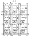
- Referring to FIG. 2, the
motherboard 200 of the OELD according to an embodiment of the present invention has a plurality ofOELDs 210. EachOELD 210 has ascan driving unit 220, atest unit 230, adata distribution unit 240, apixel unit 250, afirst wire group 260 and asecond wire group 270. - The
first wire group 260 is formed in a vertical direction (the first direction), and commonly connected to theOELDs 210 positioned in the same column on themotherboard 200. Thesecond wire group 270 is formed in a lateral direction (the second direction), and commonly connected to theOELDs 210 positioned in the same row on themotherboard 200. The first and second wire groups, 260 and 270, supply the power supply voltages and the signals for the sheet unit test to at least one of thescan driving units 220,test units 230,data distribution units 240 andpixel units 250, which are formed on each of theOELDs 210. - The
scan driving unit 220 receives the scan control signals, the third power supply voltage (VDD) and the fourth power supply voltage (VSS) from thefirst wire group 260 and/or thesecond wire group 270. Thescan driving unit 220 generates the scanning signals in response to the scan control signal, the third power supply voltage (VDD) and the fourth power supply voltage (VSS). The scanning signals generated by thescan driving unit 220 are supplied to thepixel unit 250. - The
test unit 230 receives the test control signal and test signals from thefirst wire group 260 and/or thesecond wire group 270. The test signals, which test whether or not defects in the OELD are present, can include, for example, lighting test signals, aging test signals and leakage current test signals and other test signals of the pixels included in thepixel unit 250. Thetest unit 230 supplies the test signals to thedata distribution unit 240 in response to the test control signals. - The
data distribution unit 240 receives at least two selected signals from thefirst wire group 260 and/or thesecond wire group 270. Thedata distribution unit 240 receiving the selected signals supplies the test signals, which are supplied to the output lines of eachtest unit 230, to at least two data lines. Thedata distribution unit 240 supplies the data signals, which are supplied to the output lines of each data driving unit, to at least two data lines in response to at least two selected signals supplied from the outside when the data driving unit (not shown) is inserted. Hereinafter, for convenience of description, it will be assumed that thedata distribution unit 240 supplied the test signals, which are supplied to only one output line, to three data lines. - The
pixel unit 250 is composed of a plurality of pixels (not shown) including the organic light emitting diodes. One pixel has red, green and blue subpixels, and can further include a white subpixel. Thepixel unit 250 receives the first power supply voltage (ELVDD) and the second power supply voltage (ELVSS) supplied from thefirst wire group 260 and/or thesecond wire group 270; the scanning signals supplied from thescan driving unit 220; and the test signals supplied from thedata distribution unit 240, and then displays corresponding images. - The
OELD 210 can further include the data driving unit. The data driving unit generates the data signals in response to the data supplied from the outside, after eachOELD 210 has been scribed from themotherboard 200. The data signals generated by the data driving unit are supplied to thedata distribution unit 240. As an example, the data driving unit can be mounted to overlap with thetest unit 230. - The
motherboard 200 of such an OELD can supply the power supply voltages and the signals for their tests to a plurality of theOELDs 210 formed on themotherboard 200 via thefirst wire group 260 and thesecond wire group 270. Therefore, sheet unit tests can be conducted without scribing eachOELD 210. Accordingly, this improves the efficiency of the tests by reducing the test time and lowering the cost. Also, if the circuit wires are changed, or the size of theOELD 210 is varied, the test can still be conducted without changing the test equipment or jig if the sizes of the circuit wires of thefirst wire group 260 and thesecond wire group 270, and themotherboard 200 are not changed. - Each
OELD 210, which is formed on themotherboard 200, is scribed after the sheet unit tests have been completed. The scribing lines 280 are arranged so that thescan driving unit 220, thetest unit 230, thedata distribution unit 240 and thepixel unit 250 are electrically isolated from thefirst wire group 260 and thesecond wire group 270 after theOELD 210 has been scribed. That is to say, electrical nodes between thefirst wire group 260 and thesecond wire group 270; and thescan driving unit 220, thetest unit 230, thedata driving unit 240 and thepixel unit 250 are positioned outside of the scribing line of theOELD 210. Therefore, noise, such as static electricity, which is input to thefirst wire group 260 and thesecond wire group 270 from the outside is not supplied to thescan driving unit 220, thetest unit 230, thedata distribution unit 240 and thepixel unit 250. - FIG. 3 is a view of the first embodiment of the OELD and the wire groups of FIG. 2. The same parts as those of FIG. 2 have the same reference numerals, and their descriptions have been omitted below.
- Referring to FIG. 3, the
OELD 210 according to the first embodiment has thefirst wire group 260 and thesecond wire group 270 which include a plurality of wires. - The
first wire group 260 includes afirst wire 261 for receiving the first power supply voltage (ELVDD),second wires 262 for receiving at least two selected signals,third wires 263 for receiving the test control signals and the test signals, afourth wire 264 for receiving the third power supply voltage (VDD), afifth wire 265 for receiving the fourth power supply voltage(VSS),sixth wires 266 for receiving the scan control signals, and aseventh wire 267 for receiving the second power supply voltage (ELVSS). - The
first wire 261 supplies the first power supply voltage (ELVDD), which is supplied during the sheet unit test, to thepixel units 250 formed in eachOELD 210. The first power supply voltage (ELVDD) supplied to thepixel unit 250 is supplied to the pixels formed in thepixel unit 250. - The
second wires 262 supply at least two selected signals to thedata distribution unit 240 so that the test signals supplied to each output line (O1 to Om) of thetest unit 230 can be supplied to at least two data lines (D). Thedata distribution unit 240 receives three selected signals since thedata distribution unit 240 supplies the test signal, which is supplied to one output line (O), to three data lines (D). For this purpose, thesecond wires 262 each are composed of three wires. - The
third wires 263 receive the test control signals and the test signals from the outside, and then supply them to thetest unit 230 formed in eachOELD 210. For this purpose, thethird wires 263 each are composed of two wires. - The
fourth wire 264 supplies the third power supply voltage (VDD), which is supplied during the sheet unit test, to thescan driving units 220 formed in eachOELD 210. - The
fifth wire 265 supplies the fourth power supply voltage (VSS), which is supplied during the sheet unit test, to thescan driving units 220 formed in eachOELD 210. - The
sixth wires 266 receives the scan control signals from the outside, and then supply them into thescan driving units 220 formed in eachOELD 210. Clock signals, output enable signals and start pulses of thescan driving unit 220 can be included in the scan control signals. Actually, the number of scan control signals supplied to thescan driving unit 220 can be set to a wide range depending on the circuit configuration of thescan driving unit 220. Accordingly, the number of the wires included in thesixth wires 266 is determined depending on the circuit configuration of thescan driving unit 220. - Hereinafter, for convenience of description, it is assumed that three wires are included in the
sixth wires 266. - The
seventh wire 267 supplies the second power supply voltage (ELVSS), which is supplied during the sheet unit test, to thepixel units 250 formed in eachOELD 210. The second power supply voltage (ELVSS) supplied to thepixel unit 250 is supplied to the pixels formed in thepixel unit 250. - The
second wire group 270 includes aneleventh wire 271 for receiving the first power supply voltage (ELVDD),twelfth wires 272 for receiving at least two selected signals,thirteenth wires 273 for receiving the test control signals and the test signals, afourteenth wire 274 for receiving the third power supply voltage(VDD), afifteenth wire 275 for receiving the fourth power supply voltage(VSS),sixteenth wires 276 for receiving the scan control signals, and aseventeenth wire 277 for receiving the second power supply voltage (ELVSS). - The
eleventh wire 271 supplies the first power supply voltage (ELVDD), which is supplied during the sheet unit test, to thepixel unit 250 formed in eachOELD 210. For this purpose, theeleventh wire 271 is electrically connected to thefirst wire 261. The first power supply voltage(ELVDD) supplied to thepixel unit 250 is supplied to the pixels formed in thepixel unit 250. - The
twelfth wires 272 supply three selected signals to thedata distribution units 240 so that the test signals supplied to each output line (O1 to Om) of thetest unit 230 can be supplied to three data lines (D). For this purpose, thetwelfth wires 272 are electrically connected to thesecond wires 262. That is to say, thetwelfth wires 272 are each composed of three wires which are identical to the number ofsecond wires 262, and each of thetwelfth wires 272 is electrically connected to one of thesecond wires 262. - The
thirteenth wires 273 receive the test control signals and the test signals from the outside, and then supply them to thetest unit 230 formed in eachOELD 210. For this purpose, thethirteenth wires 273 are electrically connected to thethird wires 263. That is to say, thethirteenth wires 273 each are composed of two wires which are identical to the number ofthird wires 263, and each of thethirteenth wires 273 is electrically connected to one of thethird wires 263. - The
fourteenth wire 274 supplies the third power supply voltage (VDD), which is supplied during the sheet unit test, to thescan driving unit 220 formed in eachOELD 210. For this purpose, thefourteenth wire 274 is electrically connected to thefourth wire 264. - The
fifteenth wire 275 supplies the fourth power supply voltage (VSS), which is supplied during the sheet unit test, to thescan driving unit 220 formed in eachOELD 210. For this purpose, thefifteenth wire 275 is electrically connected to thefifth wire 265. - The
sixteenth wires 276 receive the scan control signals from the outside, and then supply them to thescan driving unit 220 formed in eachOELD 210. For this purpose, thesixteenth wires 276 are electrically connected to thesixth wires 266. That is to say, thesixteenth wires 276 are each composed of three wires which are identical to the number ofsixth wires 266, and each of thesixteenth wires 276 is electrically connected to one of thesixth wires 266. - The
seventeenth wire 277 supplies the second power supply voltage (ELVSS), which is supplied during the sheet unit test, to thepixel unit 250 formed in eachOELD 210. For this purpose, theseventeenth wire 277 is electrically connected to theseventh wire 267. The second power supply voltage (ELVSS) supplied to thepixel unit 250 is supplied to the pixels formed in thepixel unit 250. - The numbers of the wires included in the
second wires 262, thethird wires 263, thesixth wires 266, thetwelfth wires 272, thethirteenth wires 273 and thesixteenth wires 276 are not limited to those of the embodiments of the present invention. That is to say, the number of wires can be set to a wide range to correspond to the kind of the test, the number of distributed data lines and the circuit configuration of thescan driving unit 220. - In such a first embodiment of the present invention, the
scan driving unit 220, thetest unit 230, thedata distribution unit 240 and thepixel unit 250 receive the power supply voltages and the signals from the wires included in thesecond wire group 270. The electrical nodes of thesecond wire group 270 are arranged so that the electrical nodes are electrically isolated from thescan driving unit 220, thetest unit 230, thedata distribution unit 240 and thepixel unit 250 after theOELD 210 has been scribed. Accordingly, the noise input from the outside after scribing is not transmitted to thescan driving unit 220, thetest unit 230, thedata distribution unit 240 and thepixel unit 250. - As described above, the first to seventh wires (261 to 267) and the eleventh to
seventeenth wires 271 to 277 of the first embodiment are arranged in a mesh configuration to electrically connect the wires receiving the same power supply voltages or signals. Therefore, the sheet unit test can be conducted according to themotherboard 200 of the OELD according to the first embodiment of the present invention. Also, a voltage drop (IR drop), a signal delay (RC delay) and other problems can be minimized by forming the power supply voltage lines and the signal lines all in the mesh configuration so that the power supply voltage lines and the signal lines can be included in thefirst wire group 260 and thesecond wire group 270. - FIG. 4 is a view of the second embodiment of the OELD and the wire groups of FIG. 2. The same parts as in FIG. 2 have the same reference numerals, and therefore their descriptions have been omitted below.
- Referring to FIG. 4, the
OELD 210 according to the second embodiment has thefirst wire group 260 and thesecond wire group 270 which include a plurality of wires. - The
first wire group 260 includes afirst wire 261 for receiving the first power supply voltage (ELVDD),second wires 262 for receiving at least two selected signals,third wires 263 for receiving the test control signals and the test signals, afourth wire 264 for receiving the third power supply voltage (VDD), afifth wire 265 for receiving the fourth power supply voltage (VSS),sixth wires 266 for receiving the scan control signals, and aseventh wire 267 for receiving the second power supply voltage (ELVSS). The signals or the power supply voltages supplied to such afirst wire group 260 are identical to those of FIG. 3, and therefore their descriptions have been omitted below. - The
second wire group 270 has aneleventh wire 271 for receiving the first power supply voltage (ELVDD), afourteenth wire 274 for receiving the third power supply voltage (VDD), afifteenth wire 275 for receiving the fourth power supply voltage (VSS), and aseventeenth wire 277 for receiving the second power supply voltage (ELVSS). - The
eleventh wire 271 supplies the first power supply voltage (ELVDD), which is supplied during the sheet unit test, to thepixel unit 250 formed in eachOELD 210. For this purpose, the eleventh wire 271is electrically connected to thefirst wire 261. The first power supply voltage (ELVDD) supplied to thepixel unit 250 is supplied to the pixels formed in thepixel unit 250. - The
fourteenth wire 274 supplies the third power supply voltage (VDD), which is supplied during the sheet unit test, to thescan driving unit 220 formed in eachOELD 210. For this purpose, thefourteenth wire 274 is electrically connected to thefourth wire 264. - The
fifteenth wire 275 supplies the fourth power supply voltage (VSS), which is supplied during the sheet unit test, to thescan driving unit 220 formed in eachOELD 210. For this purpose, thefifteenth wire 275 is electrically connected to thefifth wire 265. - The
seventeenth wire 277 supplies the second power supply voltage (ELVSS), which is supplied during the sheet unit test, to thepixel unit 250 formed in eachOELD 210. For this purpose, theseventeenth wire 277 is electrically connected to theseventh wire 267. The second power supply voltage (ELVSS) supplied to thepixel unit 250 is supplied to the pixels formed in thepixel unit 250. - The
eleventh wire 271 and thefourteenth wire 274 on the one hand; and thefifteenth wire 275 and theseventeenth wire 277 on the other hand are positioned in alternate rows, so as to arrange the power supply voltage lines more easily and to use spaces in which the power supply voltage lines are arranged more effectively. For example, theeleventh wire 271 and thefourteenth wire 274 can be arranged in the odd-numbered rows, and thefifteenth wire 275 and theseventeenth wire 277 can be arranged in the even-numbered rows. Also, theeleventh wire 271 and thefourteenth wire 274 can be arranged in the even-numbered rows, and thefifteenth wire 275 and theseventeenth wire 277 can be arranged in the odd-numbered rows. - In the second embodiment of the present invention, the
scan driving unit 220 receives the fourth power supply voltage (VSS) and the scan control signals from thefifth wires 265 and thesixth wires 266 out of thefirst wire group 260. Thescan driving unit 220 receives the third power supply voltage (VDD) from thefourteenth wire 274 out of thesecond wire group 270. - The
test unit 230 receives the test control signals and the test signals from thethird wires 263 out of thefirst wire group 260. - The
data distribution unit 240 receives the selected signals from thesecond wires 262 out of thefirst wire group 260. - The
pixel unit 250 receives the second power supply voltage (ELVSS) from theseventh wire 267 out of thefirst wire group 260, and receives the first power supply voltage (ELVDD) from theeleventh wire 271 out of the second wire group. - The electrical nodes of the
first wire group 260 and/or thesecond wire group 270 and thefirst wire group 260 are arranged outside a scribing line of theOELD 210 so that the electrical nodes are electrically isolated from thescan driving unit 220, thetest unit 230, thedata distribution unit 240 and thepixel unit 250 after theOELD 210 has been scribed. - As described above, in the second embodiment, the signal lines (namely, the
second wires 262, thethird wires 263 and the sixth wires 266) are included only in thefirst wire group 260. The power supply voltage lines (namely, thefirst wire 261, thefourth wire 264, thefifth wire 265, theseventh wire 267, theeleventh wire 271, thefourteenth wire 274, thefifteenth wire 275 and the seventeenth wire 277) are formed in a mesh configuration so that they can be included in both thefirst wire group 260 and thesecond wire group 270. - Actually, the signals can normally drive the
scan driving unit 220, thetest unit 230 and thedata distribution unit 240, though the voltage drop (IR drop) and other drops occur, if only a certain level of voltage is sustained. Accordingly, in this embodiment, the signal lines are included only in thefirst wire group 260. Therefore, the manufacturing cost and dead space are reduced, and also effectiveness of the design is secured since the number of wires included in thesecond wire group 270 is reduced compared to that of the first embodiment of FIG. 3. Also, theOELDs 210 can be tested in the unit of columns since the signal lines are formed only in one direction (namely, the first direction). That is to say, a predetermined test can be conducted only on theOELDs 210 positioned in certain columns by supplying the signals to the signal lines positioned in the certain columns. - If a voltage drop (IR drop) occurs in the power supply voltages supplied to both the
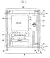
first wire group 260 and thesecond wire group 270, then there arises a problem in that desired images are not displayed. Accordingly, in this embodiment, desired images can be displayed by arranging the power supply voltage lines in both the first direction and the second direction in a mesh configuration. The power supply voltage lines can be more easily arranged and the space in which the power supply voltage lines are arranged can be utilized more effectively by alternating theeleventh wire 271 and thefourteenth wire 274; and thefifteenth wire 275 and theseventeenth wire 277 in different rows. - FIG. 5 is a view of a third embodiment of the OELD and the wire groups of FIG. 2. In the description of FIG. 5, the descriptions of the same parts as in FIG. 4 have been omitted below.
- Referring to FIG. 5, the
OELD 210 according to the third embodiment of the present invention has atransmission gate 275 connected to at least one of the wires included in thefirst wire group 260, and aneighteenth wire 278 and anineteenth wire 279 included in thesecond wire group 270 to drive thetransmission gate 275. - In the third embodiment of the present invention, the
transmission gate 275 is connected to one of the wires included in thefirst wire group 260 to control whether or not the signals (or the power supply voltages)are supplied to theOELD 210 from the connected wires. For example, thetransmission gate 275 can be positioned in any one of thesixth wires 266 for supplying the scan control signals. As described above, it is possible to conduct the test on the certain OELD in themotherboard 200 if thetransmission gate 275 is connected to one of thesixth wires 266 to control whether or not the scan control signals are supplied. That is to say, turn-on/off of thetransmission gate 275 can be controlled to select theOELD 210 in the unit of row since the scanning signals are not generated in thescan driving unit 220 which does not receive the scan control signals. Although thetransmission gate 275 is connected to one of the wires included in thefirst wire group 260 for illustration purposes, thetransmission gate 275 can actually be connected to any one or all of the wires included in thefirst wire group 260. - The
eighteenth wire 278 and thenineteenth wire 279 are included in thesecond wire group 270, and connected to the gate terminal of thetransmission gate 275 to supply control signals (CP, /CP) for controlling turn-on/off of thetransmission gate 275. - The test procedure on the
certain OELD 210 is described in detail as follows. At first, the power supply voltages are supplied to themotherboard 200. The control signals (CP, /CP) are supplied to theeighteenth wire 278 and thenineteenth wire 279 which are positioned in the certain rows, and simultaneously the signals are supplied only to the signal lines (namely, thesecond wires 262, thethird wires 263 and the sixth wires 266) positioned in the certain columns. Then, a predetermined test is performed only on theOELD 210 positioned in the points where the certain rows and the certain columns cross over. That is to say, in the third embodiment of the present invention, the test on the certain OELD can be conducted on themotherboard 200 by installing at least onetransmission gate 275 to be connected to at least one of the wires included in thefirst wire group 260. - In the third embodiment, the
scan driving unit 220 receives the fourth power supply voltage (VSS) and the scan control signals from thefifth wire 265 and thesixth wires 266 out of thefirst wire group 260. Thescan driving unit 220 receives the third power supply voltage (VDD) from thefourteenth wire 274 out of thesecond wire group 270. - The
test unit 230 receives the test control signals and the test signals from thethird wires 263 out of thefirst wire group 260. - The
data distribution unit 240 receives the selected signals from thesecond wires 262 out of thefirst wire group 260. - The
pixel unit 250 receives the second power supply voltage (ELVSS) from theseventh wire 267 out of thefirst wire group 260, and receives the first power supply voltage (ELVDD) from theeleventh wire 271 out of thesecond wire group 270. - At least one of the
scan driving unit 220, thetest unit 230, thedata distribution unit 240 and thepixel unit 250 controls whether or not the signals (or the power supply voltages) are supplied using thetransmission gate 275. - The electrical nodes of the
second wire group 260 are arranged outside a scribing line of theOELD 210 so that the electrical nodes are electrically isolated from thescan driving unit 220, thetest unit 230, thedata distribution unit 240 and thepixel unit 250 after theOELD 210 has been scribed. - As described above, in the third embodiment of the present invention, the test on the
certain OELD 210 can be conducted on themotherboard 200 by having at least onetransmission gate 275 connected to at least one of the wires included in thefirst wire group 260. - FIG. 6 is a view of a fourth embodiment of the OELD and the wire groups of FIG. 2.
- Referring to FIG. 6, the
OELD 210 according to the fourth embodiment of the present invention has thefirst wire group 260 and thesecond wire group 270 which include a plurality of wires. - The
first wire group 260 has afirst wire 261 for receiving the first power supply voltage (ELVDD),second wires 262 for receiving at least two selected signals, afourth wire 264 for receiving the third power supply voltage (VDD), afifth wire 265 for receiving the fourth power supply voltage (VSS),sixth wires 266 for receiving the scan control signals, and aseventh wire 267 for receiving the second power supply voltage (ELVSS). - The
first wire 261 supplies the first power supply voltage (ELVDD), which is supplied during the sheet unit test, to thepixel unit 250 formed in eachOELD 210. The first power supply voltage (ELVDD) supplied to thepixel unit 250 is supplied to the pixels formed in thepixel unit 250. - The
second wires 262 supply at least two selected signals to thedata distribution unit 240 so that the test signals supplied to each output line (O1 to Om) of thetest unit 230 can be supplied to at least two data lines (D). Thedata distribution unit 240 receives three selected signals because the test signal supplied to one output line (O) is supplied to three data lines (D). For this purpose, thesecond wires 262 each are composed of three wires. - The
fourth wire 264 supplies the third power supply voltage (VDD), which is supplied during the sheet unit test, to thescan driving unit 220 formed in eachOELD 210. - The
fifth wire 265 supplies the fourth power supply voltage (VSS), which is supplied during the sheet unit test, to thescan driving unit 220 formed in eachOELD 210. - The
sixth wires 266 receive the scan control signals from the outside, and then supply them to thescan driving unit 220 formed in eachOELD 210. Clock signals, output enable signals and start pulses of thescan driving unit 220 can be included in the scan control signals. Actually, the number of scan control signals supplied to thescan driving unit 220 can be set to a wide range depending on the circuit configuration of thescan driving unit 220. Accordingly, the number of wires included in thesixth wires 266 is determined depending on the circuit configuration of thescan driving unit 220. - In the present invention, it is assumed that three wires are included in the
sixth wires 266 for convenience of description. - The
seventh wire 267 supplies the second power supply voltage (ELVSS), which is supplied during the sheet unit test, to thepixel unit 250 formed in eachOELD 210. The second power supply voltage (ELVSS) supplied to thepixel unit 250 is supplied to the pixels formed in thepixel unit 250. - The
second wire group 270 has aneleventh wire 271 for receiving the first power supply voltage (ELVDD),thirteenth wires 273 for receiving the test control signals and the test signals, afourteenth wire 274 for receiving the third power supply voltage (VDD), afifteenth wire 275 for receiving the fourth power supply voltage (VSS), and aseventeenth wire 277 for receiving the second power supply voltage (ELVSS). - The
eleventh wire 271 supplies the first power supply voltage (ELVDD), which is supplied during the sheet unit test, to thepixel unit 250 formed in eachOELD 210. For this purpose, theeleventh wire 271 is electrically connected to thefirst wire 261. The first power supply voltage (ELVDD) supplied to thepixel unit 250 is supplied to the pixels formed in thepixel unit 250. - The
thirteenth wires 273 receive the test control signals and the test signals from the outside, and then supply them to thetest unit 230 formed in eachOELD 210. For this purpose, thethirteenth wires 273 are each composed of two wires. - The
fourteenth wire 274 supplies the third power supply voltage (VDD), which is supplied during the sheet unit test, to thescan driving unit 220 formed in eachOELD 210. For this purpose, thefourteenth wire 274 is electrically connected to thefourth wire 264. - The
fifteenth wire 275 supplies the fourth power supply voltage (VSS), which is supplied during the sheet unit test, to thescan driving unit 220 formed in eachOELD 210. For this purpose, thefifteenth wire 275 is electrically connected to thefifth wire 265. - The
seventeenth wire 277 supplies the second power supply voltage (ELVSS), which is supplied during the sheet unit test, to thepixel unit 250 formed in eachOELD 210. For this purpose, theseventeenth wire 277 is electrically connected to theseventh wire 267. The second power supply voltage (ELVSS) supplied to thepixel unit 250 is supplied to the pixels formed in thepixel unit 250. - The
eleventh wire 271 and thefourteenth wire 274; and thefifteenth wire 275 and theseventeenth wire 277 are alternately positioned in different rows so as to arrange the power supply voltage lines more easily and to effectively use spaces in which the power supply voltage lines are arranged. For example, theeleventh wire 271 and thefourteenth wire 274 can be arranged in the odd-numbered rows, and thefifteenth wire 275 and theseventeenth wire 277 can be arranged in the even-numbered rows. Also, theeleventh wire 271 and thefourteenth wire 274 can be arranged in the even-numbered rows, and thefifteenth wire 275 and theseventeenth wire 277 can be arranged in the odd-numbered rows. - In the fourth embodiment, the
scan driving unit 220 receives the fourth power supply voltage (VSS) and the scan control signals from thefifth wire 265 and thesixth wires 266 out of thefirst wire group 260. Thescan driving unit 220 receives the third power supply voltage (VDD) from thefourteenth wire 274 out of thesecond wire group 270. - The
test unit 230 receives the test control signals and the test signals from thethirteenth wires 273 out of thesecond wire group 270. - The
data distribution unit 240 receives the selected signals from thesecond wires 262 out of thefirst wire group 260. - The
pixel unit 250 receives the second power supply voltage (ELVSS) from theseventh wire 267 out of thefirst wire group 260, and receives the first power supply voltage (ELVDD) from theeleventh wire 271 out of thesecond wire group 270. - The electrical nodes of the
first wire group 260 and/or thesecond wire group 270 are arranged outside a scribing line of theOELD 210 so that the electrical nodes are electrically isolated from thescan driving unit 220, thetest unit 230, thedata distribution unit 240 and thepixel unit 250 after theOELD 210 has been scribed. - As described above, each of the power supply voltage lines included in the
first wire group 260 is electrically connected to one of the power supply voltage lines included in thesecond wire group 270 in the fourth embodiment of the present invention. That is to say, the power supply voltage lines are formed in both of the first direction and the second direction in a mesh configuration. Therefore, a desired pattern of images can be displayed. - In the fourth embodiment of the present invention, the
thirteenth wires 273, which are the signal lines out of thesecond wire group 270, are not connected to the wires included in thefirst wire group 260. As a result, the test on acertain OELD 210 can be conducted on themotherboard 200 without adding wires. - In accordance with the invention, a test procedure on a
certain OELD 210 is conducted as follows. At first, the power supply voltages are supplied to themotherboard 200. The test control signals and the test signals are supplied to thethirteenth wires 273 positioned in certain rows, and simultaneously the signals are supplied only in the signal lines (namely, thesecond wires 262 and the sixth wires 266) positioned in certain columns. Then, a predetermined test is performed only on theOELD 210 positioned on the points where the certain rows and the certain columns cross over. - FIG. 7 is a circuit diagram of an example of the test units of FIGs. 2 to 6.
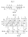
- Referring to FIG. 7, the
test unit 230 has a plurality of transistors (M 1 to Mm). They are shown in FIG. 7 as PMOS transistors. However, the present invention is not limited thereto. - The gate electrodes of the plurality of transistors (M1 to Mm) are connected to test
control signal lines 263a included in the third wires 263 (or, the thirteenth wire 273). The first electrodes of the plurality of transistors (M1 to Mm) are connected to testsignal lines 263b included in the third wires 263 (or, the thirteenth wire 273), and the second electrodes of the plurality of transistors (M1 to Mm) are connected to output lines (O1 to Om). - The test procedure is described in detail as follows. At first, the third power supply voltage (VDD), the fourth power supply voltage (VSS) and the scan control signals are supplied to the
scan driving unit 220 from the fourth wire 264 (or the fourteenth wire 274), the fifth wire 265 (or the fifteenth wire 275) and the sixth wire 266 (or the sixteenth wire 276), respectively. Thescan driving unit 220 then generates the scanning signals and supplies them to thepixel unit 250. - The test control signals (TEST_GATE) (a low level) are supplied to the transistors (M1 to Mm) from the test
control signal line 263a to turn on the transistors (M1 to Mm). - If the transistors (M1 to Mm) turned on, then the test signals (TEST_DATA) supplied to the
test signal line 263b are supplied to the output lines (O1 to Om). - Subsequently, the test signals (TEST_DATA) supplied to the output lines (O1 to Om) are supplied to the data lines (D1 to D3m) via the
data distribution unit 240 to correspond to three selected signals. - The pixels, which are included in each
OELD 210 to receive the scanning signals and the test signals (TEST_DATA) then emit light in a predetermined form to correspond to the test signals (TEST_DATA). For example, the pixels emit light to correspond to lighting test signals if the lighting test signals are supplied as the test signals (TEST_DATA). Some pixels may not emit light in a desired form. As a result, it can be confirmed whether or not hot pixels are present. Also, the white valance of the pixels can be measured and progressive defects can be also sensed since the same lighting test signals are supplied to the pixels. - Aging test signals are also supplied as the test signals (TEST_DATA). The aging test signals, which supply a high bias voltage or bias current to the data lines (D1 to D3m), detect the progressive defects of the organic light emitting diode. Also, it may be confirmed whether or not the organic light emitting diodes operate normally during changes in the temperature by setting a
substrate 200 to the level of low temperature or high temperature, followed by supplying the lighting test signals. - Leakage current test signals can also be supplied as the test signals (TEST_DATA). The leakage current test is conducted by measuring the currents flowing into the first wire 261 (or the eleventh wire 271) and the seventh wire 267 (or the seventeenth wire 277) when the first power supply voltage (ELVDD) and the second power supply voltage (ELVSS) remain to be supplied to the pixels. That is to say, when the first power supply voltage (ELVDD) and the second power supply voltage (ELVSS) remain to be supplied, the leakage current can be measured by measuring the currents flowing into the first wire 261 (or the eleventh wire 271) and the seventh wire 267 (or the seventeenth wire 277) after the
test unit 230 is turned off as a whole. - FIG. 8 is a circuit diagram of an example of the test unit and the data distribution unit of FIGs. 2 to 6.
- Referring to FIG. 8, the
data distribution unit 240 includes transistor groups (G1 to Gm) respectively connected to output lines (O1 to Om) of eachtest unit 230. - The transistor groups (G1 to Gm) each include three transistors, and each transistor is connected to one of the red, green and blue pixels. That is to say, each of three data lines connected to three transistors is respectively connected to each of the red, green and blue pixels.
- Each of the transistor groups (G1 to Gm) has the first transistors (M11, M21, ..., Mm1) connected to the red-selected
signal lines 262a included in thesecond wires 262; the second transistors (M12, M22 ..., Mm2) connected to the green-selectedsignal lines 262b included in thesecond wires 262; and the third transistors (M13, M23 ..., Mm3) connected to the blue-selectedsignal lines 262c included in thesecond wires 262. - Each of the first transistors (M11, M21, ..., Mm1) is turned on to supply the test signals, which are supplied from the output lines (O1 to Om) of the test unit, to the red pixels connected to the data lines (D3, D6, ..., D3m) when red-selected signals (SLRs) are supplied from the red-selected
signal lines 262a. - Each of the second transistors (M12, M22, ..., Mm2) is turned on to supply the test signals, which are supplied from the output lines (O1 to Om) of the test unit, to the green pixels connected to the data lines (D2, D5, ..., D3m-1) when the green-selected signals (SLGs) are supplied from the green-selected
signal lines 262b. - Each of the third transistors (M13, M23, ..., Mm3) is turned on to supply the test signals, which are supplied from the output lines (O1 to Om) of the test unit, to the blue pixels connected to the data lines (D1, D4, ..., D3m-2) when the blue-selected signals (SLBs) are supplied from the blue-selected
signal lines 262c. - The red-selected signals (SLRs), the green-selected signals (SLGs) and the blue-selected signals (SLBs) are supplied at different times. As described above, if the red-selected signals (SLRs), the green-selected signals (SLGs) and the blue-selected signals (SLBs) are supplied at different times, then the test signals supplied to each output line (O) can be divided and supplied to three data lines (D).
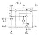
- FIG. 9 is a circuit diagram of an example of a pixel used to explain a lighting test. For convenience, FIG. 9 shows the pixels connected to the nth scanning line, the nth light emitting control line and the mth data line.
- Referring to FIG. 9, the pixels each have an organic light emitting diode; and
pixel circuits 910 connected to the n-1st scanning line (Sn-1), the nth scanning line (Sn), the nth light emitting control line (Emn), the mth data lines (Dm), the first power supply voltage (ELVDD), the reset power supply voltage (Vinit) and the organic light emitting diode. - The first electrode of the organic light emitting diode is connected to the
pixel circuit 910, and the second electrode is connected to the second power supply voltage (ELVSS). The organic light emitting diode generates a predetermined light corresponding to the current supplied to thepixel circuit 910. - The
pixel circuit 910 has first to sixth transistors (T1 to T6) and a first capacitor (C1). - The gate electrode of the first transistor (T1) is connected to the first node (N1). The first electrode of the first transistor (T1) is connected to the second node (N2), and the second electrode is connected to the third node (N3). The first transistor (T1) controls the currents flowing into the third node (N3) from the second node (N2) to correspond to the voltages supplied to its gate electrode.
- The gate electrode of the second transistor (T2) is connected to the nth scanning line (Sn). The first electrode of the second transistor (T2) is connected to the mth data lines (Dm), and the second electrode is connected to the second node (N2). The second transistor (T2) is turned on to supply the data signals, which are supplied to the mth data lines (Dm), to the second node (N2) when the scanning signals are supplied to the nth scanning lines (Sn).
- The gate electrode of the third transistor (T3) is connected to the nth scanning line (Sn). The first electrode of the third transistor (T3) is connected to the third node (N3), and the second electrode is connected to the first node (N1). The third transistor (T3) is turned on to connect the first transistor (T1) as a diode when the scanning signals are supplied to the nth scanning line (Sn).
- The gate electrode of the fourth transistor (T4) is connected to the n-1st scanning line (Sn-1). The first electrode of the fourth transistor (T4) is connected to the reset power supply voltage (Vinit), and the second electrode is connected to the first node (N1). The fourth transistor (T4) is turned on to supply the voltage of the reset power supply voltage (Vinit) to the first node (N1) when the scanning signals are supplied to the n-1st scanning line (Sn-1).
- The gate electrode of the fifth transistor (T5) is connected to the nth light emitting control line (Emn). The first electrode of the fifth transistor (T5) is connected to the fourth node (N4), and the second electrode is connected to the second node (N2). The fifth transistor (T5) is turned on to supply the first power supply voltage (ELVDD) to the second node (N2) when the light emitting control signals are not supplied to the nth light emitting control line (Emn) (That is to say, when low levels of signals are input to the nth light emitting control line (Emn)).
- The gate electrode of the sixth transistor (T6) is connected to the nth light emitting control line (Emn). The first electrode of the sixth transistor (T6) is connected to the third node (N3), and the second electrode is connected to an anode electrode of the organic light emitting diode. The sixth transistor (T6) is turned on to electrically connect the organic light emitting diode to the third node (N3) when the light emitting control signals are not supplied to the nth light emitting control line (Emn).
- One side terminal of the first capacitor (C1) is connected to the fourth node (N4), and the other side terminal is connected to the first node (N1). The first capacitor (C1) charges to voltages corresponding to the data signals and a threshold voltage (Vth) of the first transistor (T1), and sustains the charged voltages during one frame when the scanning signals are supplied to the nth canning line (Sn).
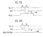
- FIG. 10A is a waveform of control signals for controlling a pixel circuit when the pixels of FIG. 9 are normally operated. FIG. 10B is a waveform of control signals for controlling the pixel circuit shown in FIG. 9 when the lighting test is conducted. Hereinafter, an operation mode of the pixel of FIG. 9 will described in detail in combination with FIG. 9 and FIGs. 10A and 10B.
- Referring to FIG. 10A, the scanning signals (SSs) are first supplied to the n-1st scanning line (Sn-1), and the light emitting control signals (EMIs) are first supplied to the nth light emitting control line (Emn) during a T1 period. If the light emitting control signals (EMIs) are supplied to the nth light emitting control line (Emn), then the fifth and sixth transistors (T5, T6) are turned off. If the scanning signals (SSs) are supplied to the n-1st scanning line (Sn-1), then the fourth transistor (T4) is turned on. If the fourth transistor (T4) is turned on, then a voltage of the first node (N1) is changed to a reset power supply voltage (Vinit). The reset power supply voltage (Vinit) is set to have a lower voltage value than a voltage value of the data signal.
- Subsequently, the scanning signals (SSs) are supplied to the nth scanning line (Sn) during a T2 period. If the scanning signals (SSs) are supplied to the nth scanning line (Sn), then the second and third transistors (T2, T3) are turned on.
- If the third transistor (T3) is turned on, then the first transistor (T1) is connected as a diode.
- If the second transistor (T2) is turned on, then the data signals supplied to the mth data line (Dm) are supplied to the second node (N2). The first transistor (T1) is turned on since a voltage value of the first node (N1) is changed to a voltage value of the reset power supply voltage (Vinit) (That is to say, the first node (N1) is set to have a lower voltage than a voltage of the second node (N2)). If the first transistor (T1) is turned on, then the data signals, which are supplied to the second node (N2), are supplied to the first node (N1) via the first transistor (T1) and the third transistor (T3). The first capacitor (C1) charges to a voltage corresponding to a voltage difference between the first node (N1) and the fourth node (N4) (namely, the first power supply voltage (ELVDD)).
- A voltage value of the first node (N1) is set to a value obtained by subtracting a threshold voltage of the first transistor (T1) from the data signals since the data signals are supplied to the first node (N1) via the first transistor (T1) and the third transistor (T3). Accordingly, the first capacitor (C1) is charged to voltages corresponding to the threshold voltages of the first transistor (T1) and data signals.
- Subsequently, if the light emitting control signals (EMIs) are not supplied to the nth light emitting control line (Emn), then the fifth and sixth transistors (T5, T6) are turned on. If the fifth transistor (T5) is turned on, then the first power supply voltage (ELVDD) is supplied to the second node (N2) via the fifth transistor (T5). If the sixth transistor (T6) is turned on, then the current supplied from the first transistor (T1) is supplied to the organic light emitting diode to correspond to a voltage charged by the first capacitor (C1). Accordingly, light corresponding to the data signals are generated by the organic light emitting diode regardless of the threshold voltage of the first transistor (T1).
- Referring to FIG. 10B, the scanning signals (SSs) are first supplied to the n-1st scanning line (Sn-1), and the light emitting control signals (EMIs) are supplied to the nth light emitting control line (Emn) during a T1 period. If the light emitting control signals (EMIs) are supplied to the nth light emitting control line (Emn), then the fifth and sixth transistors (T5, T6) are turned off. If the scanning signals (SSs) are supplied to the n-1st scanning line (Sn-1), then the fourth transistor (T4) is turned on. If the fourth transistor (T4) is turned on, then a voltage of the first node (N1) is changed to the reset power supply voltage (Vinit). The reset power supply voltage (Vinit) is set to have a lower voltage value than a voltage value of the data signals.
- Subsequently, the scanning signals (SSs) are supplied to the nth scanning line (Sn) during T2 period. If the scanning signals (SSs) are supplied to the nth scanning line (Sn), then the second and third transistors (T2, T3) are turned on. If the third transistor (T3) is turned on, then the first transistor (T1) is connected as a diode.
- If the second transistor (T2) is turned on, then the data signals supplied to the mth data lines (Dm) are supplied to the second node (N2). The first transistor (T1) is turned on since a voltage value of the first node (N1) is changed to the reset power supply voltage (Vinit) (That is to say, the first node (N1) is set to have a lower voltage than a voltage of the second node (N2)). If the first transistor (T1) is turned on, then the data signals, which are supplied to the second node (N2), are supplied to the first node (N1) via the first transistor (T1) and the third transistor (T3). The first capacitor (C1) charges to a voltage corresponding to a difference between the first node (N1) and the fourth node (N4) (namely, the first power supply voltage (ELVDD)).
- A voltage value of the first node (N1) is set to a value obtained by subtracting a threshold voltage of the first transistor (T1) from the data signals since the data signals are supplied to the first node (N1) via the first transistor (T1) and the third transistor (T3). Accordingly, the first capacitor (C1) is charged to voltages corresponding to the threshold voltages of the data signals and the first transistor (T1).
- The light emitting control signals (EMIs) continue to be supplied to the nth light emitting control line (Emn) to conduct the lighting test. Voltages corresponding to the data signals are then saved in the first capacitor (C1) during a T2 period, but the sixth transistor (T6) is turned off, and then the organic light emitting diode does not emit light. In this case, all pixels included in the
pixel unit 250 of each OELD 210 should be sustained in a turned-off state. Accordingly, the lighting test of theOELD 210 can be conducted by testing whether the pixels included in thepixel unit 250 are turned on or turned off. - FIG. 11 is a view of an embodiment where the sheet unit test is conducted on the motherboard of the OELD. Each of the OELDs of the motherboard of FIG. 11 is an OELD according to the fourth embodiment of the invention, as illustrated in FIG. 6.
- Referring to FIG. 11, the first power supply voltage (ELVDD) and the second power supply voltage (ELVSS) are first supplied to the first wire 261 (and/or the eleventh wire 271) and the
seventh wire 267 connected to thecertain OELD 300 formed in themotherboard 200. The power supply voltages and the signals are supplied to thesecond wires 262, the fourth wire 264 (and/or the fourteenth wire 274), thefifth wire 265, thesixth wires 266 and thethirteenth wires 273, which are respectively connected to thecertain OELD 300. The test is then conducted only on thecertain OELD 300, but the test is not conducted on theother OELDs 210. - The test procedure is described in detail as follows. At first, the first power supply voltage and the second power supply voltage are supplied to the first wire 261 (and/or the eleventh wire 271) and the
seventh wire 267 connected to thecertain OELD 300. The third power supply voltage (VDD), the fourth power supply voltage (VSS) and the scan control signals are supplied from the fourth wire 264 (and/or the fourteenth wire 274), thefifth wire 265 and thesixth wires 266 which are respectively connected to thecertain OELD 300. Thescan driving unit 220, which is provided in thecertain OELD 300, then generates the scanning signals and/or the light emitting control signals. Thetest unit 230, which is provided in thecertain OELD 300, receives the test control signals (TEST_GATE) and the test signals (TEST_DATA) from thethirteenth wire 273. Thetest unit 230 then supplies the test signal (TEST_DATA) to thedata distribution unit 240 to correspond to the test control signals (TEST_GATE). Thedata distribution unit 240 supplies the test signals (TEST_DATA), which are supplied from thetest unit 230, to thepixel unit 250 via the data lines (D1 to Dm) to correspond to the red-selected signals (SLRs), the green-selected signals (SLGs) and the blue-selected signals (SLBs) which are respectively supplied from thesecond wires 262. If the aging test signals, the leakage current test signals, the lighting test signals and other test signals are supplied as the test signals (TEST_DATA), then the aging test, the leakage current test and the lighting test can be sequentially conducted on thecertain OELD 300. in addition, various tests on the selectedOELD 300 can be conducted, and the order of the tests can be changed. - In the present invention, the test can also be conducted on the at least two
OELDs 210 formed in themotherboard 200. In this case, the power supply voltages and the signals are supplied to the first wire (and/or the eleventh wire 271), thesecond wires 262, the fourth wire 264 (and/or the fourteenth wire 274), thefifth wire 265, thesixth wires 266, theseventh wire 267 and thethirteenth wires 273 which are respectively connected to at least two OELDs 210. - FIG. 12 is a view of another embodiment where the sheet unit test is conducted on the motherboard of the OELD. Each of the OELDs of the motherboard of FIG. 12 is an OELD according to the fourth embodiment of the invention illustrated in FIG. 6.
- Referring to FIG. 12, the power supply voltages and the signals are supplied to a plurality of the first wires (and/or the eleventh wires 271), the
second wires 262, the fourth wires 264 (and/or the fourteenth wires 274), thefifth wires 265, thesixth wires 266, theseventh wires 267 and thethirteenth wires 273, which each are respectively connected to the OELD arranged in the first row and column, the OELD arranged in the second row and column, and the OELD arranged in the third row and column on themotherboard 200. - The signal for the lighting test is supplied to the OELD arranged in the first row and column as the test signal (TEST_DATA). The lighting test is then conducted on the OELD arranged in the first row and column.
- The signal for the leakage current test is supplied to the OELD arranged in the second row and column as the test signal (TEST_DATA). The leakage current test is then conducted on the OELD arranged in the second row and column.
- The signal for the aging test is supplied to the OELD arranged in the third row and column as the test signal (TEST_DATA). The aging test is then conducted on the OELD arranged in the third row and column.
- The lighting test, the leakage current test and the aging test can be conducted at the same time and sequentially. If the tests on the selected OELDs have been completed, then the tests of FIG. 12 are shifted by one column or by one row and then conducted again. Such a test is performed until the tests on all of the OELDs formed on the
motherboard 200 have been completed. - Thought technical ideas of the present invention have been described in detail with reference to the exemplary embodiments, the embodiments mentioned herein are just examples for the purpose of illustration only, and are not intended to limit the scope of the present invention. Also, it should be understood that various modifications could be made thereto without departing from the scope of the present invention, which is as set out in the appended Claims.
- As described above, the OELD and the testing method using the OELD according to the present invention can supply the power supply voltages and the signals for its tests to a plurality of the OELDs formed on the motherboard since there is a first wire group and a second wire group. Therefore, the sheet unit test can be conducted without scribing each OELD. Accordingly, it can be useful to increase the efficiency of the test, for example, the test time can be shortened and the cost can be reduced. Only the test on the certain OELD can be conducted. Also, even if the circuit wires constituting the OELD, or a size of the OELD are changed, the test can still be conducted without changing the test equipment or the jig if the circuit wires of the first wire group, the circuit wires of the second wire group, and the motherboard are not changed in their sizes.
Claims (37)
- An Organic Electro Luminescence Display (OELD) comprising:a pixel unit including a plurality of pixels adapted to receive a first power supply voltage, a second power supply voltage and scanning signals and to emit light;a scan driving unit adapted to supply the scanning signals to the pixel unit;a test unit adapted to test whether or not a defect in the pixel unit is present;a first wire group arranged in a first direction and having a floating end; anda second wire group arranged in a second direction and having a floating end.
- An OELD according to claim 1, wherein the first wire group and the second wire group are respectively electrically isolated from the pixel unit, the scan driving unit and the test unit.
- An OELD according to claim 1 or 2, further comprising a data driving unit adapted to supply data signals corresponding to externally supplied data to the pixel unit.
- An OELD according to claim 3, further comprising a data distribution unit adapted to supply the data signals supplied from the data driving unit to at least two pixels of the pixel unit, the data signals supplied from the data driving unit corresponding to at least two of the selected signals.
- An OELD according to claim 4, wherein the data distribution unit is electrically isolated from the first wire group and the second wire group.
- A method of testing at least one of a plurality of OELDs arranged on a motherboard, to determine whether or not there are any defects in any of the plurality of OELDs, the method comprising:commonly connecting each of a first wire group and a second wire group to OELDs aligned in a first direction and a second direction with respect to the plurality of OELDs on the motherboard:connecting at least one wire included in either the first wire group or the second wire group to each of the plurality of OELDs to supply a first power supply voltage and a second power supply voltage;supplying a first driving signal to at least one of the plurality of OELDs by wires of the first wire group, and supplying a second driving signal to at least one of the plurality of OELDs by wires of the second wire group; andtesting at least one of the plurality of OELDs in response to at least one of the first and the second power supply voltages, the first driving signal and the second driving signal.
- A method according to claim 6,
wherein at least one of the first wire group and the second wire group further supplies a third power supply voltage and a fourth power supply voltage to drive scan driving units arranged in each of the plurality of OELDs; and
wherein at least one of the first driving signal and the second driving signal comprises either a scan control signal or a test control signal, and a test signal to control the scan driving unit. - A method according to claim 7, wherein the scan control signal comprises at least one of clock signals, output enable signals and start pulses of the scan driving units arranged in each of the plurality of OELDs.
- A method according to claim 7 or 8, wherein the test signal initiates at least one of a lighting test, an aging test and a leakage current test.
- A method according to claim 7, wherein conducting a test on at least one of the plurality of OELDs further comprises:generating scanning signals to correspond to the third power supply voltage, the fourth power supply voltage and the scan control signal;supplying the scanning signals to a pixel unit arranged in at least one of the plurality of OELDs;supplying the test signals to the pixel unit in response to the test control signals; anddisplaying images on the pixel unit with correspond to the scanning signal and the test signal.
- A method according to claim 10, further comprising supplying the test signals to a plurality of pixels provided in the pixel unit to correspond to a plurality of the selected signals included in at least one of the first driving signals and the second driving signals.
- A method according to claim 7, wherein the second driving signal further comprises control signals to control whether or not at least one of the first power supply voltage, the second power supply voltage, the third power supply voltage, the fourth power supply voltage and the first driving signals, are supplied to the plurality of OELDs from the first wire group.
- A method according to claim 12, wherein the test is conducted in at least one of the plurality of OELDs receiving the first power supply voltage, the second power supply voltage, the third power supply voltage, the fourth power supply voltage, the first driving signals and the second driving signals to correspond to the control signals.
- An Organic Electro Luminescence Display (OELD), motherboard comprising:a plurality of OELDs each of which includes a pixel unit having a plurality of pixels adapted to receive a first power supply voltage, a second power supply voltage, scanning signals and test signals and to emit light; a scan driving unit adapted to supply the scanning signals to the pixel unit; a test unit adapted to supply the test signals to the pixel unit by data lines; and a data distribution unit adapted to supply the test signals connected between the test unit and the data lines to a plurality of the data lines, the test signals connected between the test unit and the data lines being supplied to output lines of separate test units;a first wire group connected to OELDs of the plurality of the OELDs aligned in a first direction; anda second wire group connected to the OELDs of the plurality of the OELDs aligned in a second direction;wherein at least one of the first and the second wire groups supplies predetermined test signals and predetermined power supply voltages to self-connected separate OELDs.
- A motherboard according to claim 14, wherein at least one of the wires included in the second wire group is electrically connected to at least one of the wires included in the first wire group.
- A motherboard according to claim 14 or 15, wherein the first wire group comprises:a first wire adapted to receive the first power supply voltage;a seventh wire adapted to receive the second power supply voltage;a fourth wire adapted to receive a third power supply voltage to drive the scan driving unit; anda fifth wire adapted to receive a fourth power supply voltage to drive the scan driving unit, andwherein the second wire group comprises:an eleventh wire adapted to receive the first power supply voltage;a seventeenth wire adapted to receive the second power supply voltage;a fourteenth wire adapted to receive the third power supply voltage to drive the scan driving unit; anda fifteenth wire adapted to receive the fourth power supply voltage to drive the scan driving unit.
- A motherboard according to claim 16, wherein the first wire and the eleventh wire; the seventh wire and the seventeenth wire; the fourth wire and the fourteenth wire; and the fifth wire and the fifteenth wire are connected to each other.
- A motherboard according to claim 17, wherein the scan driving unit is adapted to receive the third power supply voltage from the fourteenth wire, and to receive the fourth power supply voltage from the fifteenth wire.
- A motherboard according to claim 18, wherein the fourteenth wire and the fifteenth wire, and an electrical node of the scan driving unit are arranged outside of a scribing line of an OELD so that they are electrically isolated therefrom after the motherboard is scribed.
- A motherboard according to claim 17, 18 or 19 wherein the pixel unit is adapted to receive the first power supply voltage from the eleventh wire, and to receive the second power supply voltage from the seventeenth wire.
- A motherboard according to claim 20, wherein the eleventh wire, the seventeenth wire and an electrical node of the pixel unit are arranged outside of a scribing line of an OELD, so that they are electrically isolated therefrom after the motherboard is scribed.
- A motherboard according to claim 16, wherein the eleventh wire and the seventeenth wire are arranged in alternate rows.
- A motherboard according to claim 22, wherein the pixel unit is adapted to receive the first power supply voltage from the eleventh wire, and to receive the second power supply voltage from the seventh wire included in the first wire group.
- A motherboard according to claim 23, wherein the eleventh wire, and the seventh wire and an electrical node of the pixel unit are arranged outside of a scribing line of an OELD, so that they are electrically isolated therefrom after the motherboard is scribed.
- A motherboard according to one of Claims 16 to 24, wherein the fourteenth wire and the fifteenth wire arranged in alternate rows.
- A motherboard according to claim 25, wherein the scan driving unit is adapted to receive the third power supply voltage from the fourteenth wire, and to receive the fourth power supply voltage from the fifth wire included in the first wire group.
- A motherboard according to claim 26, wherein the fourteenth wire, the fifth wire and an electrical node of the scan driving unit are arranged outside of a scribing line of the OELD, so that they are electrically isolated therefrom after the motherboard is scribed.
- A motherboard according to claim 14, wherein either the first wire group further comprises:second wires adapted to receive at least two selected signals supplied to the data distribution unit;third wires adapted to receive the test control signals and the test signals supplied to the test unit; andsixth wires adapted to receive the scan control signals supplied to the scan driving unit; orwherein the second wire group further comprises:twelfth wires adapted to receive the at least two selected signals supplied to the data distribution unit;thirteenth wires adapted to receive the test signals supplied to the test unit; andsixteenth wires adapted to receive the scan control signals supplied to the scan driving unit.
- A motherboard according to claim 28, wherein:each second wire is connected to one of the twelfth wires;each third wire is connected to one of the thirteenth wires; andeach sixth wire is connected to one of the sixteenth wires.
- A motherboard according to claim 28, wherein:the data distribution unit is connected to one of the second wires and the twelfth wires by the first electrical node;the test unit is connected to one of the third wires and the thirteenth wires by the second electrical node; andthe scan driving unit is connected to one of the sixth wires and the sixteenth wires by the third electrical node.
- A motherboard according to claim 30, wherein the first electrical node, the second electrical node and the third electrical node are arranged outside of a scribing line of an OELD so that they are electrically isolated therefrom after the motherboard is scribed.
- A motherboard according to claim 28, 29, 30 or 31 further comprising a transmission gate adapted to connect at least one of the wires included in the first wire group to each OELD to control supplies of at least one of the signals and the power supply voltages supplied to the OELD from the connected wires.
- A motherboard according to claim 32, further comprising an eighteenth wire and a nineteenth wire included in the second wire group, the eighteenth wire and the nineteenth wire connected to gate terminals of the transmission gate to supply the control signals to control turn-on/off of the transmission gate.
- A motherboard according to claim 14, wherein the first wire group comprises second wires adapted to receive at least two selected signals supplied to the data distribution unit, and sixth wires adapted to receive the scan control signals supplied to the scan driving unit, and wherein the second wire group comprises thirteenth wires adapted to receive the test signals supplied to the test unit.
- A motherboard according to claim 34, wherein:the data distribution unit is connected to the second wires by the first electrical node;the scan driving unit is connected to the sixth wires by the second electrical node; andthe test unit is connected to the thirteenth wires by the third electrical node.
- A motherboard according to claim 35, wherein the first electrical node, the second electrical node and the third electrical node are arranged outside of a scribing line of the OELD so that they are electrically isolated therefrom after the motherboard is scribed.
- A motherboard according to one of Claims 14 to 36, wherein the test signal is adapted to initiate at least one of a lighting test, an aging test and a leakage current test.
Applications Claiming Priority (1)
| Application Number | Priority Date | Filing Date | Title |
|---|---|---|---|
| KR1020050080994A KR100636502B1 (en) | 2005-08-31 | 2005-08-31 | Organic electro luminescence display for performing sheet unit test and testing method using the same |
Publications (2)
| Publication Number | Publication Date |
|---|---|
| EP1763014A1 true EP1763014A1 (en) | 2007-03-14 |
| EP1763014B1 EP1763014B1 (en) | 2014-05-21 |
Family
ID=37560853
Family Applications (1)
| Application Number | Title | Priority Date | Filing Date |
|---|---|---|---|
| EP06254542.1A Active EP1763014B1 (en) | 2005-08-31 | 2006-08-31 | Organic electro-luminescent display (OELD) manufacturing method |
Country Status (5)
| Country | Link |
|---|---|
| US (1) | US7605599B2 (en) |
| EP (1) | EP1763014B1 (en) |
| JP (1) | JP4887027B2 (en) |
| KR (1) | KR100636502B1 (en) |
| CN (1) | CN100557666C (en) |
Cited By (3)
| Publication number | Priority date | Publication date | Assignee | Title |
|---|---|---|---|---|
| EP1843318A2 (en) * | 2006-04-07 | 2007-10-10 | Samsung SDI Co., Ltd. | Organic light emitting display device and testing method thereof |
| WO2008148263A1 (en) * | 2007-06-08 | 2008-12-11 | Truly Semiconductors Ltd. | Wiring method for checking wirings of an organic electroluminescent display |
| US8742784B2 (en) | 2009-09-02 | 2014-06-03 | Samsung Display Co., Ltd. | Organic light emitting display device |
Families Citing this family (31)
| Publication number | Priority date | Publication date | Assignee | Title |
|---|---|---|---|---|
| KR100793558B1 (en) * | 2006-09-18 | 2008-01-14 | 삼성에스디아이 주식회사 | Organic light emitting display devices and mother substrate of the same and method for fabricating the organic light emitting display device |
| JP4368908B2 (en) | 2007-01-03 | 2009-11-18 | 三星モバイルディスプレイ株式會社 | Method for manufacturing organic electroluminescent display device |
| KR100786465B1 (en) | 2007-01-03 | 2007-12-17 | 삼성에스디아이 주식회사 | Method for manufacturing organic light-emitting display device |
| US20080218495A1 (en) * | 2007-03-08 | 2008-09-11 | Wintek Corporation | Circuit capable of selectively operating in either an inspecting mode or a driving mode for a display |
| KR101076446B1 (en) * | 2007-04-13 | 2011-10-25 | 엘지디스플레이 주식회사 | Thin film transistor substrate and flat panel display comprising the same |
| CN100508675C (en) * | 2007-06-08 | 2009-07-01 | 信利半导体有限公司 | Anti-static method of organic EL display |
| JP2009211039A (en) * | 2008-03-04 | 2009-09-17 | Samsung Mobile Display Co Ltd | Organic light emitting display device |
| KR100924142B1 (en) * | 2008-04-01 | 2009-10-28 | 삼성모바일디스플레이주식회사 | Flat Panel Display device, Aging method and Lighting test method of the same |
| KR100916914B1 (en) * | 2008-04-25 | 2009-09-09 | 삼성모바일디스플레이주식회사 | Organic light emitting display device |
| JP2009271333A (en) * | 2008-05-08 | 2009-11-19 | Toshiba Mobile Display Co Ltd | El display device |
| KR101018832B1 (en) | 2008-12-03 | 2011-03-04 | 네오뷰코오롱 주식회사 | Organic electro luminescence display array substrate for examnining in sheet unit by individual electric power sources and method thereof |
| JP5433309B2 (en) | 2009-06-03 | 2014-03-05 | 株式会社ジャパンディスプレイ | Display device |
| KR101064466B1 (en) * | 2009-07-29 | 2011-09-16 | 삼성모바일디스플레이주식회사 | Organic Light Emitting Display Device |
| US8259095B2 (en) | 2009-08-20 | 2012-09-04 | Global Oled Technology Llc | Optically testing chiplets in display device |
| KR101094289B1 (en) * | 2009-10-14 | 2011-12-19 | 삼성모바일디스플레이주식회사 | One sheet test device and test method |
| KR101039338B1 (en) * | 2010-01-25 | 2011-06-08 | 주식회사 코디에스 | Probe unit testing micro pitch array |
| KR20120002069A (en) | 2010-06-30 | 2012-01-05 | 삼성모바일디스플레이주식회사 | Organic light emitting display device and driving method thereof |
| KR101843360B1 (en) | 2010-12-24 | 2018-03-30 | 삼성디스플레이 주식회사 | Array substrate, display apparatus and method of operating the display apparatus |
| KR101985921B1 (en) * | 2012-06-13 | 2019-06-05 | 삼성디스플레이 주식회사 | Organic light emitting diode display |
| KR101987434B1 (en) * | 2013-01-15 | 2019-10-01 | 삼성디스플레이 주식회사 | Organic light emitting diode display device and test method thereof |
| KR102057288B1 (en) * | 2013-02-21 | 2019-12-19 | 삼성디스플레이 주식회사 | Organic Light Emitting Display and Driving Method Thereof |
| KR102047005B1 (en) * | 2013-05-31 | 2019-11-21 | 삼성디스플레이 주식회사 | Organic Light Emitting Display Panel |
| CN103474026B (en) * | 2013-09-06 | 2015-08-19 | 京东方科技集团股份有限公司 | A kind of image element circuit and display |
| CN103474025B (en) * | 2013-09-06 | 2015-07-01 | 京东方科技集团股份有限公司 | Pixel circuit and displayer |
| CN104167170B (en) * | 2014-07-10 | 2016-08-31 | 京东方科技集团股份有限公司 | Image element circuit and driving method thereof and display device |
| CN105788510A (en) * | 2014-12-17 | 2016-07-20 | 昆山国显光电有限公司 | OLED display device and aging method thereof |
| KR102290483B1 (en) | 2015-04-28 | 2021-08-17 | 삼성디스플레이 주식회사 | Organic light emitting diode display and driving method thereof |
| CN105632383B (en) * | 2016-01-11 | 2018-09-11 | 京东方科技集团股份有限公司 | A kind of test circuit, test method, display panel and display device |
| KR102492735B1 (en) | 2017-09-12 | 2023-01-27 | 삼성디스플레이 주식회사 | Display device |
| CN108257541A (en) * | 2018-03-23 | 2018-07-06 | 京东方科技集团股份有限公司 | Display base plate, display panel and display device |
| CN113160744B (en) * | 2021-03-18 | 2023-01-31 | 京东方科技集团股份有限公司 | Display panel, driving method thereof and display device |
Citations (7)
| Publication number | Priority date | Publication date | Assignee | Title |
|---|---|---|---|---|
| US5053700A (en) * | 1989-02-14 | 1991-10-01 | Amber Engineering, Inc. | Method for wafer scale testing of redundant integrated circuit dies |
| US5608335A (en) * | 1992-12-31 | 1997-03-04 | Sgs-Thomson Microelectronics, S.A. | Method for the testing of integrated circuit chips and corresponding integrated circuit device |
| JP2000200053A (en) * | 1999-01-07 | 2000-07-18 | Futaba Corp | Production of substrate for display element and substrate for display element |
| US20030067319A1 (en) * | 2001-08-16 | 2003-04-10 | Kwang-Bo Cho | On-chip ADC test for image sensors |
| JP2004063407A (en) * | 2002-07-31 | 2004-02-26 | Nippon Seiki Co Ltd | Multiple arrangement substrate and its manufacturing method |
| US20040191963A1 (en) * | 2003-03-31 | 2004-09-30 | Osram Opto Semiconductors Gmbh | Encapsulation of thin-film electronic devices |
| EP1496495A2 (en) * | 2003-07-07 | 2005-01-12 | Samsung SDI Co., Ltd. | Organic light emitting device pixel circuit with self-compensation of threshold voltage and driving method therefor |
Family Cites Families (24)
| Publication number | Priority date | Publication date | Assignee | Title |
|---|---|---|---|---|
| JPH05183032A (en) * | 1991-12-30 | 1993-07-23 | Hitachi Ltd | Aging method of semiconductor integrated circuit device |
| JPH07326645A (en) * | 1994-05-31 | 1995-12-12 | Citizen Watch Co Ltd | Semiconductor integrated circuit and its measuring method |
| US6734925B1 (en) * | 1998-12-07 | 2004-05-11 | Samsung Electronics Co., Ltd. | Multiple testing bars for testing liquid crystal display and method thereof |
| US6265889B1 (en) * | 1997-09-30 | 2001-07-24 | Kabushiki Kaisha Toshiba | Semiconductor test circuit and a method for testing a semiconductor liquid crystal display circuit |
| JP2000269278A (en) * | 1999-03-15 | 2000-09-29 | Nec Corp | Burn-in device and semiconductor wafer |
| US7112115B1 (en) * | 1999-11-09 | 2006-09-26 | Semiconductor Energy Laboratory Co., Ltd. | Light emitting device and method of manufacturing the same |
| US6762735B2 (en) * | 2000-05-12 | 2004-07-13 | Semiconductor Energy Laboratory Co., Ltd. | Electro luminescence display device and method of testing the same |
| KR100643562B1 (en) * | 2000-11-28 | 2006-11-10 | 엘지.필립스 엘시디 주식회사 | Manufacturing Process of Liquid Crystal Cell for a Small Size Liquid Crystal Display Device |
| JP2004520624A (en) * | 2001-05-15 | 2004-07-08 | コーニンクレッカ フィリップス エレクトロニクス エヌ ヴィ | Display device having a plurality of LEDs |
| US6437431B1 (en) * | 2001-08-07 | 2002-08-20 | Lsi Logic Corporation | Die power distribution system |
| JP3548553B2 (en) * | 2001-10-10 | 2004-07-28 | Necマイクロシステム株式会社 | Semiconductor device and power supply wiring method between internal power supply terminals thereof |
| JP2003228302A (en) * | 2002-02-04 | 2003-08-15 | Toshiba Electronic Engineering Corp | Display device and manufacturing method therefor |
| JP4255683B2 (en) * | 2002-03-25 | 2009-04-15 | シャープ株式会社 | Glass wiring board connection structure and display device |
| US7125307B2 (en) * | 2002-07-15 | 2006-10-24 | Rohm Co., Ltd. | Method of bonding seal caps to a substrate of organic electroluminescent elements |
| EP1383103B1 (en) * | 2002-07-19 | 2012-03-21 | St Microelectronics S.A. | Automatic adaptation of the supply voltage of an electroluminescent panel depending on the desired luminance |
| KR100504473B1 (en) | 2002-09-30 | 2005-08-01 | 엘지전자 주식회사 | production method of organic EL display panel using glass seal-cover |
| JP2004170787A (en) * | 2002-11-21 | 2004-06-17 | Toshiba Corp | Display apparatus and its driving method |
| JP4051562B2 (en) | 2003-07-22 | 2008-02-27 | 統寶光電股▲分▼有限公司 | Lighting aging test system for flat panel display |
| KR100601368B1 (en) | 2003-09-08 | 2006-07-13 | 삼성에스디아이 주식회사 | Characteristic valuation means for electro luminescence display |
| JP2005149769A (en) * | 2003-11-11 | 2005-06-09 | Shimadzu Corp | Inspection method and inspection device of tft array |
| KR100578914B1 (en) * | 2003-11-27 | 2006-05-11 | 삼성에스디아이 주식회사 | Display device using demultiplexer |
| JP4480989B2 (en) * | 2003-11-28 | 2010-06-16 | オプトレックス株式会社 | Organic EL display device |
| TWI229199B (en) * | 2004-01-02 | 2005-03-11 | Au Optronics Corp | Testing apparatus of flat display |
| JP2005195854A (en) * | 2004-01-07 | 2005-07-21 | Mitsubishi Electric Corp | Image display apparatus and method for inspecting the same |
-
2005
- 2005-08-31 KR KR1020050080994A patent/KR100636502B1/en active IP Right Grant
- 2005-10-31 JP JP2005316711A patent/JP4887027B2/en active Active
-
2006
- 2006-08-09 US US11/501,033 patent/US7605599B2/en active Active
- 2006-08-31 EP EP06254542.1A patent/EP1763014B1/en active Active
- 2006-08-31 CN CNB2006101123663A patent/CN100557666C/en active Active
Patent Citations (7)
| Publication number | Priority date | Publication date | Assignee | Title |
|---|---|---|---|---|
| US5053700A (en) * | 1989-02-14 | 1991-10-01 | Amber Engineering, Inc. | Method for wafer scale testing of redundant integrated circuit dies |
| US5608335A (en) * | 1992-12-31 | 1997-03-04 | Sgs-Thomson Microelectronics, S.A. | Method for the testing of integrated circuit chips and corresponding integrated circuit device |
| JP2000200053A (en) * | 1999-01-07 | 2000-07-18 | Futaba Corp | Production of substrate for display element and substrate for display element |
| US20030067319A1 (en) * | 2001-08-16 | 2003-04-10 | Kwang-Bo Cho | On-chip ADC test for image sensors |
| JP2004063407A (en) * | 2002-07-31 | 2004-02-26 | Nippon Seiki Co Ltd | Multiple arrangement substrate and its manufacturing method |
| US20040191963A1 (en) * | 2003-03-31 | 2004-09-30 | Osram Opto Semiconductors Gmbh | Encapsulation of thin-film electronic devices |
| EP1496495A2 (en) * | 2003-07-07 | 2005-01-12 | Samsung SDI Co., Ltd. | Organic light emitting device pixel circuit with self-compensation of threshold voltage and driving method therefor |
Cited By (5)
| Publication number | Priority date | Publication date | Assignee | Title |
|---|---|---|---|---|
| EP1843318A2 (en) * | 2006-04-07 | 2007-10-10 | Samsung SDI Co., Ltd. | Organic light emitting display device and testing method thereof |
| US8018402B2 (en) | 2006-04-07 | 2011-09-13 | Samsung Mobile Display Co., Ltd. | Organic light emitting display device and testing method thereof |
| WO2008148263A1 (en) * | 2007-06-08 | 2008-12-11 | Truly Semiconductors Ltd. | Wiring method for checking wirings of an organic electroluminescent display |
| US8257125B2 (en) | 2007-06-08 | 2012-09-04 | Truly Industry Limited | Wiring method for checking wirings of an organic electroluminescent display |
| US8742784B2 (en) | 2009-09-02 | 2014-06-03 | Samsung Display Co., Ltd. | Organic light emitting display device |
Also Published As
| Publication number | Publication date |
|---|---|
| CN100557666C (en) | 2009-11-04 |
| KR100636502B1 (en) | 2006-10-18 |
| US7605599B2 (en) | 2009-10-20 |
| CN1924963A (en) | 2007-03-07 |
| JP4887027B2 (en) | 2012-02-29 |
| JP2007065606A (en) | 2007-03-15 |
| EP1763014B1 (en) | 2014-05-21 |
| US20070046581A1 (en) | 2007-03-01 |
Similar Documents
| Publication | Publication Date | Title |
|---|---|---|
| US7605599B2 (en) | Organic electro luminescence display (OELD) to perform sheet unit test and testing method using the OELD | |
| KR100754140B1 (en) | Organic Light Emitting Display and Mother Substrate for Performing Sheet Unit Test and Testing Method Using the Same | |
| US7995011B2 (en) | Organic light emitting display device and mother substrate of the same | |
| US9767767B2 (en) | Pixel, display device including the pixel, and method of driving the display device | |
| JP4537356B2 (en) | Organic electroluminescence display device and inspection method thereof | |
| TWI546792B (en) | Mother substrate of organic light emitting displays capable of sheet unit testing and method of sheet unit testing | |
| KR100941834B1 (en) | Mother Substrate of Organic Light Emitting Display Devices and Aging Method Thereof | |
| US9595213B2 (en) | Organic light-emitting display panel | |
| JP5770451B2 (en) | Pixel and organic light emitting display using the same | |
| US11605355B2 (en) | Organic light emitting display device and method of testing the same | |
| CN110634433A (en) | Display panel | |
| CN108109589B (en) | Display device and method for sensing element characteristics thereof | |
| US20070001711A1 (en) | Organic light emitting display array substrate and method of performing test using the same | |
| US20210241682A1 (en) | Led based display panel including common led driving circuit and display apparatus including the same | |
| CN101859529B (en) | Display apparatus and driving method for display apparatus | |
| KR20190004717A (en) | A display having a redundant light emitting device | |
| KR20160043616A (en) | Organic Light Emitting Display Panel and Test Method | |
| KR101968117B1 (en) | organic light-emitting dIODE DISPLAY device AND DRIVING METHOD OF THE SAME | |
| KR20170018126A (en) | Apparatus for array test and method for the array test | |
| KR20190043372A (en) | Organic light emitting display device and driving method | |
| KR20200113089A (en) | Display panel and method of testing display panel | |
| CN114267274A (en) | Array substrate, detection method thereof, light-emitting panel and display device | |
| KR100812058B1 (en) | Organic light emitting display |
Legal Events
| Date | Code | Title | Description |
|---|---|---|---|
| PUAI | Public reference made under article 153(3) epc to a published international application that has entered the european phase |
Free format text: ORIGINAL CODE: 0009012 |
|
| 17P | Request for examination filed |
Effective date: 20060906 |
|
| AK | Designated contracting states |
Kind code of ref document: A1 Designated state(s): AT BE BG CH CY CZ DE DK EE ES FI FR GB GR HU IE IS IT LI LT LU LV MC NL PL PT RO SE SI SK TR |
|
| AX | Request for extension of the european patent |
Extension state: AL BA HR MK YU |
|
| AKX | Designation fees paid |
Designated state(s): DE FR GB |
|
| 17Q | First examination report despatched |
Effective date: 20071128 |
|
| RAP1 | Party data changed (applicant data changed or rights of an application transferred) |
Owner name: SAMSUNG MOBILE DISPLAY CO., LTD. |
|
| RAP1 | Party data changed (applicant data changed or rights of an application transferred) |
Owner name: SAMSUNG DISPLAY CO., LTD. |
|
| GRAP | Despatch of communication of intention to grant a patent |
Free format text: ORIGINAL CODE: EPIDOSNIGR1 |
|
| INTG | Intention to grant announced |
Effective date: 20131125 |
|
| GRAS | Grant fee paid |
Free format text: ORIGINAL CODE: EPIDOSNIGR3 |
|
| GRAA | (expected) grant |
Free format text: ORIGINAL CODE: 0009210 |
|
| RIN1 | Information on inventor provided before grant (corrected) |
Inventor name: JEONG, JIN TAE Inventor name: KWAK, WON KYU |
|
| AK | Designated contracting states |
Kind code of ref document: B1 Designated state(s): DE FR GB |
|
| REG | Reference to a national code |
Ref country code: GB Ref legal event code: FG4D |
|
| REG | Reference to a national code |
Ref country code: DE Ref legal event code: R096 Ref document number: 602006041655 Country of ref document: DE Effective date: 20140626 |
|
| REG | Reference to a national code |
Ref country code: DE Ref legal event code: R097 Ref document number: 602006041655 Country of ref document: DE |
|
| PLBE | No opposition filed within time limit |
Free format text: ORIGINAL CODE: 0009261 |
|
| STAA | Information on the status of an ep patent application or granted ep patent |
Free format text: STATUS: NO OPPOSITION FILED WITHIN TIME LIMIT |
|
| 26N | No opposition filed |
Effective date: 20150224 |
|
| REG | Reference to a national code |
Ref country code: DE Ref legal event code: R097 Ref document number: 602006041655 Country of ref document: DE Effective date: 20150224 |
|
| REG | Reference to a national code |
Ref country code: FR Ref legal event code: PLFP Year of fee payment: 11 |
|
| REG | Reference to a national code |
Ref country code: FR Ref legal event code: PLFP Year of fee payment: 12 |
|
| REG | Reference to a national code |
Ref country code: FR Ref legal event code: PLFP Year of fee payment: 13 |
|
| P01 | Opt-out of the competence of the unified patent court (upc) registered |
Effective date: 20230515 |
|
| PGFP | Annual fee paid to national office [announced via postgrant information from national office to epo] |
Ref country code: GB Payment date: 20230720 Year of fee payment: 18 |
|
| PGFP | Annual fee paid to national office [announced via postgrant information from national office to epo] |
Ref country code: FR Payment date: 20230725 Year of fee payment: 18 Ref country code: DE Payment date: 20230720 Year of fee payment: 18 |