EP1760900A1 - Radio tag and radio tag communication distance modification method - Google Patents
Radio tag and radio tag communication distance modification method Download PDFInfo
- Publication number
- EP1760900A1 EP1760900A1 EP05750723A EP05750723A EP1760900A1 EP 1760900 A1 EP1760900 A1 EP 1760900A1 EP 05750723 A EP05750723 A EP 05750723A EP 05750723 A EP05750723 A EP 05750723A EP 1760900 A1 EP1760900 A1 EP 1760900A1
- Authority
- EP
- European Patent Office
- Prior art keywords
- antenna
- rfid tag
- output power
- data
- value
- Prior art date
- Legal status (The legal status is an assumption and is not a legal conclusion. Google has not performed a legal analysis and makes no representation as to the accuracy of the status listed.)
- Granted
Links
Images


Classifications
-
- G—PHYSICS
- G06—COMPUTING; CALCULATING OR COUNTING
- G06K—GRAPHICAL DATA READING; PRESENTATION OF DATA; RECORD CARRIERS; HANDLING RECORD CARRIERS
- G06K19/00—Record carriers for use with machines and with at least a part designed to carry digital markings
- G06K19/06—Record carriers for use with machines and with at least a part designed to carry digital markings characterised by the kind of the digital marking, e.g. shape, nature, code
- G06K19/067—Record carriers with conductive marks, printed circuits or semiconductor circuit elements, e.g. credit or identity cards also with resonating or responding marks without active components
- G06K19/07—Record carriers with conductive marks, printed circuits or semiconductor circuit elements, e.g. credit or identity cards also with resonating or responding marks without active components with integrated circuit chips
- G06K19/073—Special arrangements for circuits, e.g. for protecting identification code in memory
- G06K19/07309—Means for preventing undesired reading or writing from or onto record carriers
- G06K19/07345—Means for preventing undesired reading or writing from or onto record carriers by activating or deactivating at least a part of the circuit on the record carrier, e.g. ON/OFF switches
-
- G—PHYSICS
- G06—COMPUTING; CALCULATING OR COUNTING
- G06K—GRAPHICAL DATA READING; PRESENTATION OF DATA; RECORD CARRIERS; HANDLING RECORD CARRIERS
- G06K19/00—Record carriers for use with machines and with at least a part designed to carry digital markings
- G06K19/06—Record carriers for use with machines and with at least a part designed to carry digital markings characterised by the kind of the digital marking, e.g. shape, nature, code
- G06K19/067—Record carriers with conductive marks, printed circuits or semiconductor circuit elements, e.g. credit or identity cards also with resonating or responding marks without active components
- G06K19/07—Record carriers with conductive marks, printed circuits or semiconductor circuit elements, e.g. credit or identity cards also with resonating or responding marks without active components with integrated circuit chips
- G06K19/0723—Record carriers with conductive marks, printed circuits or semiconductor circuit elements, e.g. credit or identity cards also with resonating or responding marks without active components with integrated circuit chips the record carrier comprising an arrangement for non-contact communication, e.g. wireless communication circuits on transponder cards, non-contact smart cards or RFIDs
-
- G—PHYSICS
- G06—COMPUTING; CALCULATING OR COUNTING
- G06K—GRAPHICAL DATA READING; PRESENTATION OF DATA; RECORD CARRIERS; HANDLING RECORD CARRIERS
- G06K19/00—Record carriers for use with machines and with at least a part designed to carry digital markings
- G06K19/06—Record carriers for use with machines and with at least a part designed to carry digital markings characterised by the kind of the digital marking, e.g. shape, nature, code
- G06K19/067—Record carriers with conductive marks, printed circuits or semiconductor circuit elements, e.g. credit or identity cards also with resonating or responding marks without active components
- G06K19/07—Record carriers with conductive marks, printed circuits or semiconductor circuit elements, e.g. credit or identity cards also with resonating or responding marks without active components with integrated circuit chips
- G06K19/073—Special arrangements for circuits, e.g. for protecting identification code in memory
-
- G—PHYSICS
- G06—COMPUTING; CALCULATING OR COUNTING
- G06K—GRAPHICAL DATA READING; PRESENTATION OF DATA; RECORD CARRIERS; HANDLING RECORD CARRIERS
- G06K19/00—Record carriers for use with machines and with at least a part designed to carry digital markings
- G06K19/06—Record carriers for use with machines and with at least a part designed to carry digital markings characterised by the kind of the digital marking, e.g. shape, nature, code
- G06K19/067—Record carriers with conductive marks, printed circuits or semiconductor circuit elements, e.g. credit or identity cards also with resonating or responding marks without active components
- G06K19/07—Record carriers with conductive marks, printed circuits or semiconductor circuit elements, e.g. credit or identity cards also with resonating or responding marks without active components with integrated circuit chips
- G06K19/077—Constructional details, e.g. mounting of circuits in the carrier
- G06K19/07749—Constructional details, e.g. mounting of circuits in the carrier the record carrier being capable of non-contact communication, e.g. constructional details of the antenna of a non-contact smart card
- G06K19/0775—Constructional details, e.g. mounting of circuits in the carrier the record carrier being capable of non-contact communication, e.g. constructional details of the antenna of a non-contact smart card arrangements for connecting the integrated circuit to the antenna
- G06K19/07756—Constructional details, e.g. mounting of circuits in the carrier the record carrier being capable of non-contact communication, e.g. constructional details of the antenna of a non-contact smart card arrangements for connecting the integrated circuit to the antenna the connection being non-galvanic, e.g. capacitive
-
- G—PHYSICS
- G06—COMPUTING; CALCULATING OR COUNTING
- G06K—GRAPHICAL DATA READING; PRESENTATION OF DATA; RECORD CARRIERS; HANDLING RECORD CARRIERS
- G06K19/00—Record carriers for use with machines and with at least a part designed to carry digital markings
- G06K19/06—Record carriers for use with machines and with at least a part designed to carry digital markings characterised by the kind of the digital marking, e.g. shape, nature, code
- G06K19/067—Record carriers with conductive marks, printed circuits or semiconductor circuit elements, e.g. credit or identity cards also with resonating or responding marks without active components
- G06K19/07—Record carriers with conductive marks, printed circuits or semiconductor circuit elements, e.g. credit or identity cards also with resonating or responding marks without active components with integrated circuit chips
- G06K19/077—Constructional details, e.g. mounting of circuits in the carrier
- G06K19/07749—Constructional details, e.g. mounting of circuits in the carrier the record carrier being capable of non-contact communication, e.g. constructional details of the antenna of a non-contact smart card
- G06K19/07766—Constructional details, e.g. mounting of circuits in the carrier the record carrier being capable of non-contact communication, e.g. constructional details of the antenna of a non-contact smart card comprising at least a second communication arrangement in addition to a first non-contact communication arrangement
- G06K19/07767—Constructional details, e.g. mounting of circuits in the carrier the record carrier being capable of non-contact communication, e.g. constructional details of the antenna of a non-contact smart card comprising at least a second communication arrangement in addition to a first non-contact communication arrangement the first and second communication means being two different antennas types, e.g. dipole and coil type, or two antennas of the same kind but operating at different frequencies
Definitions
- the present invention relates to RFID tags which are attachable to products, cards, etc.
- RFID tags have been proposed.
- One proposal is, for example, to attach radio tags to products so that inventory control and distribution management can be done without a need of personnel.
- Utilizing RFID tags for controlling food in a home refrigerator has also been proposed.
- Patent Document 1 proposes a method for protecting information in a tag by varying communication distance of an active tag.
- An active tag disclosed in Patent Document 1 includes a battery for powering the various electronic circuits, amplifying means, a demodulator for demodulating incoming signals and a data processing unit.
- the demodulator includes validating means for validating the data included in the incoming signals.
- the data processing unit includes a circuit for controlling maximum communication distance between the tag that transmits signals at a predetermined power and a reader. This circuit transmits signals for varying a gain of the amplifying means or a reference voltage of the validating means to control the maximum communication distance.
- Patent Document 1 Japanese Patent Laid-open No. 2001-358611
- Patent Document 1 is directed to active tags, and the communication distance between the tag and the reader is controlled by varying the gain of the incoming signals based on the signals transmitted from the circuit. Such a configuration cannot be applied to passive tags. In other words, a configuration for varying the communication distance between a passive tag and a reader/writer is not proposed in Patent Document 1. Also, because an active tag requires a battery and an amplifying means, the tag itself will be high in costs.
- the active tag according to the aforementioned invention controls the gain of the incoming signals according to an operating mode. Therefore, a reader may not receive necessary data, which the reader is supposed to receive from a tag, from the tag when shortening the communication distance between the tag and the reader/writer.
- a first invention provides an RFID tag that stores data.
- This RFID tag comprises the following elements:
- the emission control means is configured to selectively use a plurality of resistors, to selectively use a plurality of antennas, or to turn provision of data to the first antenna on and off. Also, by forming a broken line for chipping a part of a coil antenna printed on a film, the output power of the first antenna will be zero when the film is torn along the broken line to destroy the first antenna. In either case, the output power of the first antenna can be adjusted for both an active tag and a passive tag.
- An RFID tag having such a configuration can shorten the transmission distance of the transmitted radio waves from the first antenna, for example, by attenuating the output power, thus an unauthorized read-out of the data from a remote place is prevented.
- the received radio waves may be provided to receiving means via the emission control means.
- the receiving means has a function for obtaining received data by demodulating the radio waves. An unauthorized write-in from a remote place using powerful radio waves will thus be prevented by controlling power of received radio waves.
- a second invention provides the RFID tag according to the first invention, wherein the emission control means has the following means:
- the attenuation means may be, for example, a plurality of resistors or a variable resistor.
- the attenuation control means selects or switches between the resistors, or adjusts the resistance value of the variable resistor.
- reflected waves of the radio waves from a reader are used for transmitting data from the tag to the reader.
- a passive tag employing a backscattering method can attenuate the output power by adjusting a resistance value of a resistor connected in parallel with the first antenna to adjust a match/mismatch of impedance.
- a third invention provides the RFID tag according to the second invention wherein the attenuation means includes a plurality of resistors.
- the attenuation control means connects the transmission means and the first antenna via at least one of the plurality of resistors.
- a passive tag employing the backscattering method can attenuate the output power of the first antenna by adjusting the resistance value of the resistor connected in parallel with the first antenna to adjust the match/mismatch of impedance.
- the transmission distance of the radio waves can be shortened by selecting a resistor R1 with a small impedance mismatch to reduce the reflected waves.
- the transmission distance of the radio waves can be extended by selecting a resistor R2 with a large impedance mismatch to increase the reflected waves. Therefore, an unauthorized read-out of data from a remote place will be prevented by selecting a resistor to attenuate the output power of the first antenna.
- a fourth invention provides the RFID tag according to the second invention wherein the attenuation means includes a variable resistor connected between the transmission means and the first antenna.
- the attenuation control means adjusts the resistance value of the variable resistor.
- a passive tag employing the backscattering method can attenuate the output power of the first antenna by adjusting the resistance value of the resistor connected in parallel with the first antenna to adjust the match/mismatch of impedance. For example, the reflected waves will be reduced and thus the transmission distance of the radio waves can be shortened by adjusting the resistance value of the variable resistor to R1 which reduces the impedance mismatch. On the other hand, the reflected waves will be increased and thus the transmission distance of the radio waves can be extended by adjusting the resistance value of the variable resistor to R2 which increases the impedance mismatch. Therefore, an unauthorized read-out of data from a remote place will be prevented by adjusting the resistance value to attenuate the output power of the first antenna.
- a fifth invention provides the RFID tag according to the first invention wherein the emission control means has connection control means for disconnecting a connection between the antenna and the transmission means.
- Provision of data to the antenna can be stopped, for example, by using switching means such as a switch. Also, by forming a broken line between an IC chip printed on a film and a coil antenna, a connection between the transmission means included in the IC chip and the antenna will be disconnected when the film is torn along the broken line.
- a sixth invention provides the RFID tag according to the fifth invention wherein the connection control means includes switching means for switching the connection between the transmission means and the antenna ON and OFF.
- Such a switch can connect or disconnect the transmission means and the antenna. As a result, flexibility of adjusting the output power will be enhanced.
- a seventh invention provides the RFID tag according to the fifth or sixth invention, and the RFID tag further comprises a second antenna for transmitting radio waves at an output power different from the output power of the first antenna, the second antenna being connected to the transmission means via the emission control means.
- This RFID tag can prevent an unauthorized read-out of data from a remote place by choosing between the antennas. For example, by using a switch as the connection control means, provision of data to at least one antenna will be stopped. Of course, there may be cases where provision of data to all the antennas is stopped. An unauthorized write-in from a remote place will thus be prevented by choosing between the antennas to select not only the power of transmitted radio waves but also the power of received radio waves.
- connection control means may have the following configuration.
- a premise is that the RFID tag comprises a first antenna electrically connected to an IC chip including the transmission means, and a second antenna magnetically coupled to the first antenna.
- the IC chip, the first antenna and the second antenna are formed on a film, and a broken line is formed between the first antenna and the second antenna. By tearing the film along the broken line, the second antenna is removed from the RFID tag so that the connection between the IC chip and the second antenna is disconnected.
- Such a configuration that enables removal of the second antenna may be one example of other configuration examples of the connection control means.
- a specific example of the first antenna may be an on-chip coil that is electrically connected to the IC chip.
- a specific example of the second antenna may be a coil antenna that is magnetically coupled to the on-chip coil therearound. Because such a film type RFID tag is usually adhered to an article, it would be easier to tear the second antenna off by applying different adhesiveness on the back side of the portion to be torn off from the rest of the tag.
- An eighth invention provides the RFID tag according to the first invention, the RFID tag further comprising determination means for determining the value of the output power of the first antenna.
- the emission control means controls the output power of the first antenna based on the value determined by the determination means.
- the determination means may read out the value of the output power stored in storage means or determine the value in accordance with a predetermined event. For example, the value of the output power may be set in accordance with an authentication result by the RFID tag that authenticates the reader. Conceivably, the determination means may determine the value of the output power based on whether or not a tag ID is included in data that the RFID tag receives or based on importance of data to be transmitted. In the case of determining the value of the output power based on the stored values of output power, the value of the output power may be written into the storage means externally. For example, the value of the output power may be written into the RFID tag from a writer provided at a gate for a predetermined area. A CPU included in the IC chip of the RFID tag makes it possible to determine the value of the output power in various ways thus enabling flexible control of the output power.
- a ninth invention provides the RFID tag according to the eighth invention, the RFID tag further comprising storage means for storing values of output powers of the first antenna.
- the determination means determines the output power based on the values stored in the storage means.
- a tenth invention provides the RFID tag according to the eighth invention, the RFID tag further comprising authentication means for authenticating an external device to which the radio waves from the first antenna are transmitted.
- the determination means determines the value of the output power according to an authentication result determined by the authentication means.
- radio waves may be increased for the authenticated reader and reduced for the unauthenticated reader.
- the determination means limits the value of the output powerto "low” in the case of an unauthenticated reader. Thereby, an electromotive force in the RFID tag will increase and start an authentication circuit in the tag.
- the determination means changes the value of the output power to "high” when the authentication circuit authenticate s the reader. Thereby, a flexible processing using the RFID tag becomes possible by securing long communication distance after the authentication, as well as making it much harder for an unauthenticated reader at a remote place to illegally read out authentication information.
- An eleventh invention provides the RFID tag wherein the determination means determines the value of the output power according to an attribute of the data.
- the value of the output power may be set to "low” when transmitting highly confidential information, and "high” when transmitting information with low confidentiality.
- an unauthorized read-out of important information will be prevented.
- an unauthorized write-in to important data from a remote place will be prevented by adjusting the received emission level in accordance with the kind of data to be received.
- attributes of data such as degree of confidentiality, expiration date, a degree of openness are correlated with the data and stored.
- a twelfth invention provides the RFID tag according to the eighth invention wherein the first antenna further receives radio waves.
- This RFID tag further comprises receiving means for obtaining received data by demodulating the radio waves received by the first antenna. Also in this tag, the determination means determines the value of the output power based on the received data.
- the determination means decides the value of the output power to be "low”.
- the determination means decides the value of the output power to be "high”.
- the reader whose tag ID is recognized is considered to be an authorized external device.
- a thirteenth invention provides the RFID tag according to the eighth invention that further comprises setting-receiving means for receiving settings of the values of the output power from the external device.
- the determination means determines the value of the output power based on the received settings of the values.
- the settings of emission level may be received externally and the value of the output power may be determined based on them.
- the first antenna is a UHF-band antenna for a long distance and the second antenna is a 13.5 MHz-band antenna for a short distance.
- the determination means receives from an external device settings regarding ON/OFF of the first antenna for a long distance, and switches the first antenna on or off. Before switching the first antenna on or off, the external device may be authenticated and the first antenna may be switched on or off based on an authentication result.
- the RFID tag is attached to a student's bag and the reader/writer is set up at a school entrance.
- the RFID tag authenticates the reader/writer and switches the first antenna for a long distance on in accordance with the settings from the reader/writer.
- the RFID tag authenticates the reader/writer and switches the first antenna for a long distance off according to the settings from the reader/writer.
- the RFID tag of the present invention is capable of preventing an unauthorized read-out of data from a remote place by controlling the emission level. Also, this configuration can be applied to both active and passive tags.
- Fig. 1 is a block diagram of an RFID tag according to the first embodiment of the present invention.
- An RFID tag 1 has an antenna (corresponding to the first antenna), a receiving unit (corresponding to the receiving means and the setting-receiving means), a transmission unit (corresponding to the transmission means), a storage unit (corresponding to the storage means), an authentication unit (corresponding to the authentication means), a control unit (corresponding to the determination means) and an emission control unit (corresponding to the emission control means) .
- the receiving unit, the transmission unit and the storage unit may be collectively called a control block.
- the antenna is achieved by an on-chip coil or a coil
- the control block and the authentication unit is achieved by an electric circuit such as an IC chip having a CPU.
- the antenna transmits and receives radio waves.
- the receiving unit obtains received data by demodulating a signal received by the antenna, and provides it with the control unit.
- the transmission unit generates a transmission signal by modulating data read from the storage unit ortransmission data such as a processing result of the received data, and provides the transmission signal to the antenna 11 via the emission control unit.
- the storage unit stores various data such as a tag ID that identifies an RFID tag, product information and user information.
- the stored data may include attributes of data, for example, data kind, degree of importance, confidentiality and openness, and expiration date, etc.
- the storage unit may also store settings of emission levels to control the output power of the antenna. By adjusting the output power of the antenna based on the settings stored in the tag, it will be easier to prevent important information in the tag from being illegally read out from a remote place.
- the settings of levels in the storage unit may be prestored therein or may be written into from a reader/writer outside the tag. For example, the settings of emission levels may be written into the storage unit of the RFID tag from a writer set up at a gate of a given area.
- the authentication unit authenticates a reader/writer of the RFID tag based on the received data.
- the control unit writes data into the storage unit in accordance with a command included in the received data or reads out data from the storage unit and passes it to the transmission unit.
- the control unit may also determine the value of the output power of the antenna and notify it to the emission control unit.
- a method for determining the value of the output power in other words the value of the emission level, is not particularly limited.
- the control unit may read out a value of output power stored in the storage unit and decide it to be the value of the output power, or determine the value of the output power according to a predetermined event.
- One example of determining the emission level according to a predetermined event is to set the emission level according to an authentication result from the authentication unit authenticating a reader/writer.
- the emission level is determined according to whether or not a tag ID is included in data that the RFID tag receives, or attribute information of data to be transmitted.
- the control unit may also update values of emission levels stored in the storage unit using the aforementioned methods. Flexible control of the emission level becomes possible by determining the value of the output power by various methods performed by the control unit. Methods for determining the emission level will be described more in detail below (see (3) Determining the emission level).
- the emission control unit is connected to the antenna and the transmission unit, and controls the output power of the antenna.
- the emission control unit may have a configuration in which the output power of the antenna is controlled by an external operation, or may control the output power of the antenna based on the value of the output power that the control unit determined.
- the emission control unit is configured to selectively use a plurality of resistors or to turn provision of the transmission signal to the first antenna on and off. In either case, the output power of the antenna can be adjusted and the transmission distance can be shortened for both an active tag and a passive tag. As a result, an unauthorized read-out of data from a remote place will be prevented. Specific configurations of the emission control unit will be described more in detail below.
- Fig. 2 is an explanatory diagram showing one specific configuration example of an emission control unit.
- the elements in Fig. 2 that are identical to the elements shown in Fig. 1 are identified by the same reference numerals.
- An emission control unit 17 has a connection control unit 171 for disconnecting the connection between the antenna and the transmission unit. As shown in Fig. 1, the transmission unit is included in the control block.
- the connection control unit 171 includes a switch SW.
- the connection control unit 171 provides or stops providing the transmission signal to the antenna by opening and closing the switch based on an instruction from the control unit.
- the switch SW may be replaced with the following configuration.
- a broken line may be formed between the IC chip and the antenna as the connection control unit 171. By manually tearing the film along the broken line, the connection between the transmission means in the IC chip and the antenna is disconnected. If the broken line is formed in a way that a part of the antenna is chipped by tearing the film along the line, the emission level will be zero with the antenna being destroyed.
- connection control unit 171 can be applied to both active tags and passive tags.
- configurations of the connection control unit 171 are not limited to the aforementioned examples.
- Fig. 3 is an explanatory diagram showing another configuration example of the emission control unit.
- the elements in Fig. 3 that are identical to the elements shown in Fig. 1 are identified by the same reference numerals.
- the emission control unit 17 has an attenuation unit 172 for attenuating the output power of the antenna and attenuation control unit 173 for controlling attenuation of the output power by the attenuation unit 172.
- the attenuation unit 172 in this example includes a plurality of resistors R1 and R2 that are connected to the control block and the antenna in parallel.
- the attenuation control unit 173 in this example includes a switch SW.
- the attenuation control unit 173 connects the transmission unit and the antenna via at least one of the resistors R1 or R2.
- the attenuation control unit 173 selects or switches between the resistors in accordance with the value of the output power instructed by the control unit.
- This configuration may be applied to active tags but preferably applied to passive tags.
- load modulation using the reflected waves of radio waves from the reader is employed when transmitting data from the RFID tag to the reader.
- a passive tag employing the load modulation method can attenuate the emission level by selecting or switching between the resistors R1 or R2 connected in parallel to the antenna to adjust the match/mismatch of impedance. The same effect may be achieved by selecting or switching between the resistive loads used for the load modulation instead of selecting or switching between the resistors connected in parallel to the antenna.
- the impedance mismatch between the antenna and the control block is smaller when using the resistor R2 than when using the resistor R1.
- the attenuation control unit 173 selecting the resistor R2 the reflected waves will be reduced thus shortening the transmission distance of radio waves.
- electricity for starting up the authentication unit may be retained by selecting the resistor R2.
- the attenuation control unit 173 selecting the resistor R1 the reflected waves will be increased thus extending the transmission distance of radio waves.
- electricity may be used for transmitting the data by selecting the resistor R1. Note that the number of resistors and resistance values are adjustable as necessary.
- a variable resistor connected between the transmission unit and the antenna in parallel may be used as the attenuation unit 172 instead of using a plurality of resistors.
- the attenuation control unit 173 adjusts the resistance value of the variable resistor in accordance with an instruction of the control unit. Adjusting the resistance value of the variable resistor will have the same effect as using the plurality of resistors R1 and R2.
- the control unit may determine the value of the output power based on the settings. By adjusting the output power of the antenna 11 based on the stored values of output powers, important information in the tag will advantageously be prevented from being illegally read out from a remote place.
- the control unit may determine the output power of the antenna in accordance with an authentication result by the authentication unit authenticating an external reader/writer. For example, the control unit may set the value of the output power of the antenna to be high for an authenticated reader and low for an unauthenticated reader. With this configuration, an unauthorized read-out of data will be prevented while ensuring communication of necessary data.
- the control unit may first set the value of the output power to the reader to "low”. Thereby, an electromotive force in the RFID tag will increase and starts an authentication unit in the tag.
- the control unit changes the value of the output power to "high” when the reader is authenticated by the authentication unit.
- a flexible and secure communication using the RFID tag becomes possible while preventing authentication information from being illegally read out by an unauthorized reader from a remote place as well as securing long communication distance after the authentication.
- the control unit may determine the value of the output power of the antenna according to the attributes of transmission data. Take an example where degree of confidentiality of data in the storage unit is correlated with the data and stored therein. When transmitting highly confidential data, the control unit sets the value of the output power to "low”. When transmitting data with low confidentiality, the control unit sets the value of the output power to "high”. Thereby, an unauthorized read-out of important information will be prevented.
- the control unit may set the value of the output power to "low” when transmitting the user information and "high” when transmitting the product information. In this way, an unauthorized read-out of data relating to the privacy of user from a remote place will be prevented.
- the output power of the antenna can be changed flexibly according to the transmission data.
- the control unit may determine the value of the output power of the antenna 11 basedon the received data received by the receiving unit. For example, in the case where the receiving unit receives a command that does not include a tag ID from a reader, the control unit may determine the value of the output power to be "low” because the reader is possibly unauthorized. On the other hand, in the case where the receiving unit receives a command that includes a tag ID from a reader, the control unit may determine the value of the output power to be "high". In other words, the reader whose tag ID is recognized will be considered as an authorized reader. In this way, data is prevented from being read out by a possibly unauthorized external device from a remote place without limiting the communication distance to an authorized reader.
- the output power of the antenna can flexibly be changed depending on the received data by interpreting the received data in accordance with the needs.
- the output power of the antenna may be changed in accordance with the kind of command to be received or a source of command.
- the output power of the antenna may also be changed in accordance with various data values indicating the surrounding environment such as temperature, illuminance, humidity, precipitation, density, pollen level and dust level.
- the control unit may determine the value of the output power of the antenna based on the received emission level.
- the receiving unit 12 receives setting commands indicating the value of the output power or ON/OFF of the antenna from the external reader/writer.
- the control unit changes the output power or switches between ON and OFF of the antenna when the reader/writer is authenticated by the authentication unit.
- a configuration in which the setting commands include a tag ID of the RFID tag may also be possible.
- the RFID tag is attached to a student's bag and the reader/writer is set up at a school entrance.
- the RFID tag authenticates the reader/writer and switches the antenna on in accordance with the settings from the reader/writer.
- the RFID tag authenticates the reader/writer and switches the first antenna off according to the settings from the reader/writer.
- the student's location on the school premises can be known using the student's RFID tag.
- the student's RFID tag is prevented from being illegally read out or written in outside the school.
- settings of the power of received radio waves may be accepted and the radio waves may be received in accordance with the settings.
- Fig. 4 is a flow chart showing a processing example performed by an RFID tag 1 shown in Fig. 1.
- the value of output power of the antenna 11 is determined according to an authentication result of the authentication unit 15, but a method for determining the value of output power of an antenna 11 is not limited to this example. It has already been stated above that the emission level of the antenna 11 can be controlled by the external operation.
- Step S1 A control unit 16 waits for receipt of any data via a receiving unit 12. Upon the receipt of data, the control unit 16 judges whether or not the data includes a data transmission request command to the RFID tag 1. When the transmission request command is received, the flow moves to step S2. If the transmission request command is not received, the flow moves back to step S1 and waits for receipt of the transmission request command.
- Step S2-S3 The control unit 16 passes the received data to the authentication unit 15 and instructs authentication of a request source reader. Further, the control unit 16 obtains a determination result from the authentication unit 15. If the request source reader is authenticated (S2), the control unit 16 instructs an emission control unit 17 to set the value of output power of the antenna 11 to "high" (S3). Upon this instruction, the emission control unit 17 performs a control such as closing a switch, selecting a resistor or switching between the resistors.
- Step S4 If the request source reader is not authenticated (S3), the control unit 16 instructs the emission control unit 17 to set the value of the output power to "low” (S4). Upon this instruction, the emission control unit 17 performs a control such as opening the switch, selecting a resistor or switching between the resistors.
- Step S5 The control unit 16 reads out the requested data from a storage unit 14 and transmits the data from the antenna 11 via a transmission unit 13 and the emission control unit 17.
- An unauthorized read-out of data by an unauthenticated reader will thus be prevented by changing, in accordance with the authentication result of a reader, the output power of the antenna used for transmitting data.
- Fig. 5 is a flow chart showing another processing example performed by the RFID tag 1 shown in Fig. 1.
- the value of the output power of the antenna 11 is determined according to the attributes of transmission data.
- degree of "confidentiality" is considered as an attribute of transmission data.
- Step S11 A control unit 16 waits for receipt of any data via the receiving unit 12. Upon the receipt of data, the control unit 16 judges whether or not the data includes a data transmission request command to the RFID tag 1. When the transmission request command is received, the flow moves to step S12. If the transmission request command is not received, the flow moves back to step S11 and waits for receipt of the transmission request command.
- Step S12-S13 The control unit 16 passes the received data to the authentication unit 15 and instructs to authenticate a request source reader. Further, the control unit 16 obtains a determination result from the authentication unit 15. If the request source reader is authenticated (S12), the control unit 16 reads out the requested data and its degree of confidentiality from the storage unit 14, and determines whether or not the degree of confidentiality of the requested data is high (S13).
- Step S14 When the degree of confidentiality of the requested data is high, the control unit 16 instructs the emission control unit 17 to set the value of the output power to "high". Upon this instruction, the emission control unit 17 performs a control such as closing a switch, selecting a resistor or switching between the resistors.
- Step S15 When the degree of confidentiality of the requested data is low, the control unit 16 instructs the emission control unit 17 to set the value of the output power to "low". Upon this instruction, the emission control unit 17 performs a control such as opening the switch, selecting a resistor or switching between the resistors.
- Step S16 The control 16 transmits the data from the antenna 11 via the transmission unit 13 and the emission control unit 17.
- data can be transmitted depending on a security level required by the data and the security for data can thus be guaranteed by changing the output power of the antenna used for transmitting data in accordance with the attributes of data to be transmitted.
- the RFID tag according to the first embodiment attenuates the transmission signal of the antenna using the resistors, or turns provision of the transmission signal to the antenna on and off by using a means such as a switch. Therefore, the emission level, i.e. the output power of the antenna, can be adjusted regardless of active tags or passive tags.
- a broken line may be used as the emission control unit 17 for disconnecting a connection between the antenna and the IC chip.
- the output power of the antenna can thus be adjusted externally.
- Fig. 6 is a block diagram showing a configuration of an RFID tag according to the second embodiment.
- a configuration of an RFID tag 1' is identical with that of the first embodiment except that it has a plurality of antennas 11a and 11b (corresponding to a first antenna and a second antenna).
- the elements in Fig. 6 having the same function as those in Fig. 1 are identified by the same reference numerals.
- An emission control unit 17' may have a disconnection unit 174 for disconnecting a connection between at least one antenna and a transmission unit 13.
- Fig. 7 is a configuration example of the disconnection unit 174.
- the disconnection unit 174 includes switches SW1 and SW2. The switches SW1 and SW2 connect or disconnect the first antenna 11a and the transmission unit 13, or the second antenna 11b and the transmission unit 13. By selecting the switch SW1 or the switch SW2, the disconnection unit 174 can stop providing data to at least one antenna. Of course, there may be cases where provision of data to all the antennas is stopped.
- the RFID tag thus configured controls the output power of the antennas by selectively using the plurality of antennas 11a and 11b and prevents data from being illegally read out from a remote place.
- the emission control unit 17' Similar to the RFID tag in Fig. 1, it is possible to provide the emission control unit 17' with the attenuation unit 172 including a plurality of resistors and switches, and the attenuation control unit 173 so that some or all of the output power of the plurality of antennas is attenuated. Note that a configuration in which the emission control unit 17' controls the output power of the antennas in accordance with the external operation or the instruction from the control unit 16 is the same as that of the first embodiment.
- Fig. 8 is an explanatory diagram showing one example of the output power control using an RFID tag having a plurality of antennas.
- settings of the emission level are received externally, and the emission control unit determines the emission level based on the settings.
- the RFID tag is attached to a student's bag and a reader/writer is set up at a school entrance. Between the two antennas of the RFID tag, one is a UHF-band antenna for a long distance and the other is a 13.5 MHz-band antenna for a short distance.
- the RFID tag receives the settings from the reader/writer using the antenna for a short distance and switches the antenna for a long distance on.
- the RFID tag When the student leaves the school, the RFID tag switches the antenna for a long distance off according to the settings from the reader/writer. With this configuration, the student's RFID tag is prevented from being illegally read out or written in from a remote place when the student is outside the school. On the other hand, when the student is on the school premises, the student's presence can be detected using the antenna for a long distance.
- the RFID tag may authenticate the reader before switching the antenna for a long distance on or off, and switch between the settings in accordance with an authentication result.
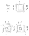
- Fig. 9 is an explanatory diagram showing another example of a control of the output power using the RFID tag having a plurality of antennas.
- Fig. 9 (a) shows a configuration of the RFID tag 1.
- the RFID tag 1 comprises, on a film body, an IC chip 30 including elements other than the antenna, a first antenna 11a electrically connected to the IC chip 30 and a second antenna 11b magnetically coupled to the first antenna 11a.
- Figs. 9(b) and 9(c) show that the second antenna 11b can be removed from the IC chip 30 by tearing the film along the perforated line 175.
- a connection between the second antenna 11b and the transmission unit 13 can be disconnected.
- a specific example of the first antenna 11b may be an on-chip coil.
- a specific example of the second antenna 11b may be a coil antenna. Because such a film type RFID tag 1 is usually adhered to an article, it would be easier to remove the second antenna from the article by applying different adhesiveness on the back side of the portion to be torn off from the rest of the tag.
- Fig. 10 is an explanatory diagram showing that the output power of the RFID tag 1 as a whole is controlled by tearing, along the perforated line, only the second antenna 11b off the film type RFID tag 1 adhered on the article.
- a position of the perforated line 175 as the emission control unit 17' for controlling the output power of the antenna is not limited to the position shown in Fig. 9(a).
- Fig. 9(d) shows another example of position of the perforated line 175 for controlling the output power of the RFID tag 1.
- the perforated line 175 may be formed at such a position that at least one side of the antenna 11b is broken by tearing the film along the line.
- FIG. 11 shows a configuration example of the RFID tag 1 of Fig. 1 in which the antenna 11 and the receiving unit 12 are connected via the emission control unit 17. With this configuration, a distance of the radio waves that the antenna 11 receives can be adjusted.
- a configuration example of the emission control unit 17 may be the emission control unit 171 shown in Fig. 2.
- Fig. 12 shows a configuration example of the RFID tag 1' of Fig. 6 in which the antennas 11a and 11b, and the receiving unit 12 are connected via the emission control unit 17'. With this configuration, a distance of the radio waves that the antennas 11a and 11b receive can be adjusted.
- a configuration example of the emission control unit 17' may be the configuration shown in Fig. 7.
- the reception distance can be adjusted by selecting or switching between antennas in the aforementioned manner thus preventing an unauthorized write-in into the RFID tags 1 or 1' from a remote place.
- the present invention can be applied to both active tags and passive tags.
Abstract
Description
- The present invention relates to RFID tags which are attachable to products, cards, etc.
- Recently, various usages of RFID tags have been proposed. One proposal is, for example, to attach radio tags to products so that inventory control and distribution management can be done without a need of personnel. Utilizing RFID tags for controlling food in a home refrigerator has also been proposed.
- Meanwhile, as usage of RFID tags diversifies, problems associated with it have arisen. A privacy issue discussed below is pointed out as one of such problems. Namely, because information in a RFID tag can be read from places apart from the tag, it is possible that what is inside one's bag is known by a third party or one's behavior is tracked based on information that the tag transmits. In order to solve the aforementioned problem,
Patent Document 1, for example, proposes a method for protecting information in a tag by varying communication distance of an active tag. - An active tag disclosed in
Patent Document 1 includes a battery for powering the various electronic circuits, amplifying means, a demodulator for demodulating incoming signals and a data processing unit. The demodulator includes validating means for validating the data included in the incoming signals. The data processing unit includes a circuit for controlling maximum communication distance between the tag that transmits signals at a predetermined power and a reader. This circuit transmits signals for varying a gain of the amplifying means or a reference voltage of the validating means to control the maximum communication distance.
Patent Document 1:Japanese Patent Laid-open No. 2001-358611 - However, the invention disclosed in
Patent Document 1 is directed to active tags, and the communication distance between the tag and the reader is controlled by varying the gain of the incoming signals based on the signals transmitted from the circuit. Such a configuration cannot be applied to passive tags. In other words, a configuration for varying the communication distance between a passive tag and a reader/writer is not proposed inPatent Document 1. Also, because an active tag requires a battery and an amplifying means, the tag itself will be high in costs. - The active tag according to the aforementioned invention controls the gain of the incoming signals according to an operating mode. Therefore, a reader may not receive necessary data, which the reader is supposed to receive from a tag, from the tag when shortening the communication distance between the tag and the reader/writer.
- It is an object of the present invention to provide a technology enabling adjustment of the communication distance between both an active tag and a passive tag, and a reader/writer.
- It is another object of the present invention to provide a technology whereby reliability of communication between a tag and a reader/writer is guaranteed while controlling the communication distance.
- In order to solve the aforementioned problems, a first invention provides an RFID tag that stores data. This RFID tag comprises the following elements:
- * a first antenna for transmitting radio waves;
- * transmission means for generating a transmission signal by modulating the data, and providing the transmission signal to the first antenna; and
- * emission control means for controlling an output power of the first antenna in order to transmit the transmission signal, the emission control means being connected to the first antenna and the transmission means.
- Conceivably, the emission control means is configured to selectively use a plurality of resistors, to selectively use a plurality of antennas, or to turn provision of data to the first antenna on and off. Also, by forming a broken line for chipping a part of a coil antenna printed on a film, the output power of the first antenna will be zero when the film is torn along the broken line to destroy the first antenna. In either case, the output power of the first antenna can be adjusted for both an active tag and a passive tag.
- An RFID tag having such a configuration can shorten the transmission distance of the transmitted radio waves from the first antenna, for example, by attenuating the output power, thus an unauthorized read-out of the data from a remote place is prevented.
- When the first antenna receives the radio waves, the received radio waves may be provided to receiving means via the emission control means. Here, the receiving means has a function for obtaining received data by demodulating the radio waves. An unauthorized write-in from a remote place using powerful radio waves will thus be prevented by controlling power of received radio waves.
- A second invention provides the RFID tag according to the first invention, wherein the emission control means has the following means:
- * attenuation means for attenuating the output power of the first antenna; and
- * attenuation control means for controlling attenuation of the output power by the attenuation means.
- The attenuation means may be, for example, a plurality of resistors or a variable resistor. In accordance with the output power of the first antenna, the attenuation control means selects or switches between the resistors, or adjusts the resistance value of the variable resistor. For a passive tag, reflected waves of the radio waves from a reader are used for transmitting data from the tag to the reader. A passive tag employing a backscattering method can attenuate the output power by adjusting a resistance value of a resistor connected in parallel with the first antenna to adjust a match/mismatch of impedance.
- A third invention provides the RFID tag according to the second invention wherein the attenuation means includes a plurality of resistors. In such an RFID tag, the attenuation control means connects the transmission means and the first antenna via at least one of the plurality of resistors.
- A passive tag employing the backscattering method can attenuate the output power of the first antenna by adjusting the resistance value of the resistor connected in parallel with the first antenna to adjust the match/mismatch of impedance. For example, the transmission distance of the radio waves can be shortened by selecting a resistor R1 with a small impedance mismatch to reduce the reflected waves. On the other hand, the transmission distance of the radio waves can be extended by selecting a resistor R2 with a large impedance mismatch to increase the reflected waves. Therefore, an unauthorized read-out of data from a remote place will be prevented by selecting a resistor to attenuate the output power of the first antenna.
- A fourth invention provides the RFID tag according to the second invention wherein the attenuation means includes a variable resistor connected between the transmission means and the first antenna. In such an RFID tag, the attenuation control means adjusts the resistance value of the variable resistor.
- A passive tag employing the backscattering method can attenuate the output power of the first antenna by adjusting the resistance value of the resistor connected in parallel with the first antenna to adjust the match/mismatch of impedance. For example, the reflected waves will be reduced and thus the transmission distance of the radio waves can be shortened by adjusting the resistance value of the variable resistor to R1 which reduces the impedance mismatch. On the other hand, the reflected waves will be increased and thus the transmission distance of the radio waves can be extended by adjusting the resistance value of the variable resistor to R2 which increases the impedance mismatch. Therefore, an unauthorized read-out of data from a remote place will be prevented by adjusting the resistance value to attenuate the output power of the first antenna.
- A fifth invention provides the RFID tag according to the first invention wherein the emission control means has connection control means for disconnecting a connection between the antenna and the transmission means.
- Provision of data to the antenna can be stopped, for example, by using switching means such as a switch. Also, by forming a broken line between an IC chip printed on a film and a coil antenna, a connection between the transmission means included in the IC chip and the antenna will be disconnected when the film is torn along the broken line.
- A sixth invention provides the RFID tag according to the fifth invention wherein the connection control means includes switching means for switching the connection between the transmission means and the antenna ON and OFF.
- Such a switch can connect or disconnect the transmission means and the antenna. As a result, flexibility of adjusting the output power will be enhanced.
- A seventh invention provides the RFID tag according to the fifth or sixth invention, and the RFID tag further comprises a second antenna for transmitting radio waves at an output power different from the output power of the first antenna, the second antenna being connected to the transmission means via the emission control means.
- This RFID tag can prevent an unauthorized read-out of data from a remote place by choosing between the antennas. For example, by using a switch as the connection control means, provision of data to at least one antenna will be stopped. Of course, there may be cases where provision of data to all the antennas is stopped. An unauthorized write-in from a remote place will thus be prevented by choosing between the antennas to select not only the power of transmitted radio waves but also the power of received radio waves.
- Another example of the connection control means may have the following configuration. A premise is that the RFID tag comprises a first antenna electrically connected to an IC chip including the transmission means, and a second antenna magnetically coupled to the first antenna. The IC chip, the first antenna and the second antenna are formed on a film, and a broken line is formed between the first antenna and the second antenna. By tearing the film along the broken line, the second antenna is removed from the RFID tag so that the connection between the IC chip and the second antenna is disconnected. Such a configuration that enables removal of the second antenna may be one example of other configuration examples of the connection control means.
- A specific example of the first antenna may be an on-chip coil that is electrically connected to the IC chip. A specific example of the second antenna may be a coil antenna that is magnetically coupled to the on-chip coil therearound. Because such a film type RFID tag is usually adhered to an article, it would be easier to tear the second antenna off by applying different adhesiveness on the back side of the portion to be torn off from the rest of the tag.
- An eighth invention provides the RFID tag according to the first invention, the RFID tag further comprising determination means for determining the value of the output power of the first antenna. In this RFID tag, the emission control means controls the output power of the first antenna based on the value determined by the determination means.
- The determination means may read out the value of the output power stored in storage means or determine the value in accordance with a predetermined event. For example, the value of the output power may be set in accordance with an authentication result by the RFID tag that authenticates the reader. Conceivably, the determination means may determine the value of the output power based on whether or not a tag ID is included in data that the RFID tag receives or based on importance of data to be transmitted. In the case of determining the value of the output power based on the stored values of output power, the value of the output power may be written into the storage means externally. For example, the value of the output power may be written into the RFID tag from a writer provided at a gate for a predetermined area. A CPU included in the IC chip of the RFID tag makes it possible to determine the value of the output power in various ways thus enabling flexible control of the output power.
- A ninth invention provides the RFID tag according to the eighth invention, the RFID tag further comprising storage means for storing values of output powers of the first antenna. In this RFID tag, the determination means determines the output power based on the values stored in the storage means.
- It will become easier to protect important information in the tag from being illegally read out from a remote place by adjusting the output power of the antenna based on the values stored in the tag.
- A tenth invention provides the RFID tag according to the eighth invention, the RFID tag further comprising authentication means for authenticating an external device to which the radio waves from the first antenna are transmitted. In this RFID tag, the determination means determines the value of the output power according to an authentication result determined by the authentication means.
- For example, radio waves may be increased for the authenticated reader and reduced for the unauthenticated reader. With this configuration, an unauthorized read-out of data will be prevented while ensuring communication of necessary data.
- More specifically, the determination means limits the value of the output powerto "low" in the case of an unauthenticated reader. Thereby, an electromotive force in the RFID tag will increase and start an authentication circuit in the tag. The determination means changes the value of the output power to "high" when the authentication circuit authenticate s the reader. Thereby, a flexible processing using the RFID tag becomes possible by securing long communication distance after the authentication, as well as making it much harder for an unauthenticated reader at a remote place to illegally read out authentication information.
- Let us assume that the aforementioned configuration is applied to a bracelet type tag. An authentication is performed by contacting the tag to a reader. When an authentication result is "OK", the reader detects a login. As long as the authenticated reader detects the tag in a given area, it maintains the login. When the tag is no longer detected, it is assumed that the tag has logged out.
- An eleventh invention provides the RFID tag wherein the determination means determines the value of the output power according to an attribute of the data.
- For example, the value of the output power may be set to "low" when transmitting highly confidential information, and "high" when transmitting information with low confidentiality. Thus, an unauthorized read-out of important information will be prevented. Similarly, an unauthorized write-in to important data from a remote place will be prevented by adjusting the received emission level in accordance with the kind of data to be received. In performing this processing, attributes of data such as degree of confidentiality, expiration date, a degree of openness are correlated with the data and stored.
- A twelfth invention provides the RFID tag according to the eighth invention wherein the first antenna further receives radio waves. This RFID tag further comprises receiving means for obtaining received data by demodulating the radio waves received by the first antenna. Also in this tag, the determination means determines the value of the output power based on the received data.
- For example, when the RFID tag receives a command transmitted by a reader whose tag ID is not recognized, the determination means decides the value of the output power to be "low". On the other hand, when the RFID tag receives a command including specification of tag ID, the determination means decides the value of the output power to be "high". In other words, the reader whose tag ID is recognized is considered to be an authorized external device. With this configuration, the communication distance to a possibly unauthorized external device can be limited without limiting the communication distance to the authorized external device.
- A thirteenth invention provides the RFID tag according to the eighth invention that further comprises setting-receiving means for receiving settings of the values of the output power from the external device. In this tag, the determination means determines the value of the output power based on the received settings of the values.
- The settings of emission level may be received externally and the value of the output power may be determined based on them. For example, the first antenna is a UHF-band antenna for a long distance and the second antenna is a 13.5 MHz-band antenna for a short distance. The determination means receives from an external device settings regarding ON/OFF of the first antenna for a long distance, and switches the first antenna on or off. Before switching the first antenna on or off, the external device may be authenticated and the first antenna may be switched on or off based on an authentication result.
- The following application example is given. The RFID tag is attached to a student's bag and the reader/writer is set up at a school entrance. When the student arrives at the school, the RFID tag authenticates the reader/writer and switches the first antenna for a long distance on in accordance with the settings from the reader/writer. When the student leaves the school, the RFID tag authenticates the reader/writer and switches the first antenna for a long distance off according to the settings from the reader/writer. With this configuration, the student's RFID tag is prevented from being illegally read out or written in from a remote place.
- The RFID tag of the present invention is capable of preventing an unauthorized read-out of data from a remote place by controlling the emission level. Also, this configuration can be applied to both active and passive tags.
-
- Fig. 1 is a block diagram of an RFID tag according to the first embodiment.
- Fig. 2 is an explanatory diagram showing a configuration example of an emission control unit of Fig. 1.
- Fig. 3 is an explanatory diagram of another configuration example of the emission control unit of Fig. 1.
- Fig. 4 is a flow chart showing a processing example performed by the RFID tag shown in Fig. 1.
- Fig. 5 is a flow chart showing another processing example performed by the RFID tag shown in Fig. 1.
- Fig. 6 is a block diagram of a configuration of an RFID tag according to the second embodiment.
- Fig. 7 is a configuration example of a connection-disconnecting unit included in an emission control unit of Fig. 6.
- Fig. 8 is an explanatory diagram showing one example of a control of transmitted emission using an RFID tag having a plurality of antennas.
- Fig. 9 is an explanatory diagram showing another example of a control of transmitted emission using the RFID tag having a plurality of antennas.
- Fig. 10 is an explanatory diagram showing one example of an emission control of an RFID tag.
- Fig. 11 shows a configuration example of an RFID tag that controls reception distance.
- Fig. 12 shows another configuration example of the RFID tag that controls reception distance.
- Fig. 1 is a block diagram of an RFID tag according to the first embodiment of the present invention. An
RFID tag 1 has an antenna (corresponding to the first antenna), a receiving unit (corresponding to the receiving means and the setting-receiving means), a transmission unit (corresponding to the transmission means), a storage unit (corresponding to the storage means), an authentication unit (corresponding to the authentication means), a control unit (corresponding to the determination means) and an emission control unit (corresponding to the emission control means) . Hereinafter, the receiving unit, the transmission unit and the storage unit may be collectively called a control block. The antenna is achieved by an on-chip coil or a coil, and the control block and the authentication unit is achieved by an electric circuit such as an IC chip having a CPU. - The antenna transmits and receives radio waves.
- The receiving unit obtains received data by demodulating a signal received by the antenna, and provides it with the control unit.
- The transmission unit generates a transmission signal by modulating data read from the storage unit ortransmission data such as a processing result of the received data, and provides the transmission signal to the
antenna 11 via the emission control unit. - The storage unit stores various data such as a tag ID that identifies an RFID tag, product information and user information. The stored data may include attributes of data, for example, data kind, degree of importance, confidentiality and openness, and expiration date, etc. The storage unit may also store settings of emission levels to control the output power of the antenna. By adjusting the output power of the antenna based on the settings stored in the tag, it will be easier to prevent important information in the tag from being illegally read out from a remote place. The settings of levels in the storage unit may be prestored therein or may be written into from a reader/writer outside the tag. For example, the settings of emission levels may be written into the storage unit of the RFID tag from a writer set up at a gate of a given area.
- The authentication unit authenticates a reader/writer of the RFID tag based on the received data.
- The control unit writes data into the storage unit in accordance with a command included in the received data or reads out data from the storage unit and passes it to the transmission unit. The control unit may also determine the value of the output power of the antenna and notify it to the emission control unit. Note that a method for determining the value of the output power, in other words the value of the emission level, is not particularly limited. Specifically, the control unit may read out a value of output power stored in the storage unit and decide it to be the value of the output power, or determine the value of the output power according to a predetermined event. One example of determining the emission level according to a predetermined event is to set the emission level according to an authentication result from the authentication unit authenticating a reader/writer. Another example is that the emission level is determined according to whether or not a tag ID is included in data that the RFID tag receives, or attribute information of data to be transmitted. The control unit may also update values of emission levels stored in the storage unit using the aforementioned methods. Flexible control of the emission level becomes possible by determining the value of the output power by various methods performed by the control unit. Methods for determining the emission level will be described more in detail below (see (3) Determining the emission level).
- The emission control unit is connected to the antenna and the transmission unit, and controls the output power of the antenna. The emission control unit may have a configuration in which the output power of the antenna is controlled by an external operation, or may control the output power of the antenna based on the value of the output power that the control unit determined. Conceivably, the emission control unit is configured to selectively use a plurality of resistors or to turn provision of the transmission signal to the first antenna on and off. In either case, the output power of the antenna can be adjusted and the transmission distance can be shortened for both an active tag and a passive tag. As a result, an unauthorized read-out of data from a remote place will be prevented. Specific configurations of the emission control unit will be described more in detail below.
- Fig. 2 is an explanatory diagram showing one specific configuration example of an emission control unit. The elements in Fig. 2 that are identical to the elements shown in Fig. 1 are identified by the same reference numerals.
- An
emission control unit 17 has aconnection control unit 171 for disconnecting the connection between the antenna and the transmission unit. As shown in Fig. 1, the transmission unit is included in the control block. In this example, theconnection control unit 171 includes a switch SW. For example, theconnection control unit 171 provides or stops providing the transmission signal to the antenna by opening and closing the switch based on an instruction from the control unit. - The switch SW may be replaced with the following configuration. In the case of a film type RFID tag on which an IC chip including an element other than the antenna is mounted, and the antenna is printed, a broken line may be formed between the IC chip and the antenna as the
connection control unit 171. By manually tearing the film along the broken line, the connection between the transmission means in the IC chip and the antenna is disconnected. If the broken line is formed in a way that a part of the antenna is chipped by tearing the film along the line, the emission level will be zero with the antenna being destroyed. - The aforementioned
connection control unit 171 can be applied to both active tags and passive tags. Of course, configurations of theconnection control unit 171 are not limited to the aforementioned examples. - Fig. 3 is an explanatory diagram showing another configuration example of the emission control unit. The elements in Fig. 3 that are identical to the elements shown in Fig. 1 are identified by the same reference numerals.
- The
emission control unit 17 has anattenuation unit 172 for attenuating the output power of the antenna andattenuation control unit 173 for controlling attenuation of the output power by theattenuation unit 172. - The
attenuation unit 172 in this example includes a plurality of resistors R1 and R2 that are connected to the control block and the antenna in parallel. Theattenuation control unit 173 in this example includes a switch SW. Theattenuation control unit 173 connects the transmission unit and the antenna via at least one of the resistors R1 or R2. Theattenuation control unit 173 selects or switches between the resistors in accordance with the value of the output power instructed by the control unit. - This configuration may be applied to active tags but preferably applied to passive tags. For passive tags, load modulation using the reflected waves of radio waves from the reader is employed when transmitting data from the RFID tag to the reader. A passive tag employing the load modulation method can attenuate the emission level by selecting or switching between the resistors R1 or R2 connected in parallel to the antenna to adjust the match/mismatch of impedance. The same effect may be achieved by selecting or switching between the resistive loads used for the load modulation instead of selecting or switching between the resistors connected in parallel to the antenna.
- For example, let us assume that the impedance mismatch between the antenna and the control block is smaller when using the resistor R2 than when using the resistor R1. In this case, by the
attenuation control unit 173 selecting the resistor R2, the reflected waves will be reduced thus shortening the transmission distance of radio waves. Thus, as shown in Fig. 3(a), when authenticating a reader/writer outside the tag, electricity for starting up the authentication unit may be retained by selecting the resistor R2. On the other hand, by theattenuation control unit 173 selecting the resistor R1, the reflected waves will be increased thus extending the transmission distance of radio waves. Thus, as shown in Fig. 3(b), when authentication is not necessary, electricity may be used for transmitting the data by selecting the resistor R1. Note that the number of resistors and resistance values are adjustable as necessary. - A variable resistor connected between the transmission unit and the antenna in parallel may be used as the
attenuation unit 172 instead of using a plurality of resistors. In this case, theattenuation control unit 173 adjusts the resistance value of the variable resistor in accordance with an instruction of the control unit. Adjusting the resistance value of the variable resistor will have the same effect as using the plurality of resistors R1 and R2. - In the case where the storage unit stores settings for the value of output powers, the control unit may determine the value of the output power based on the settings. By adjusting the output power of the
antenna 11 based on the stored values of output powers, important information in the tag will advantageously be prevented from being illegally read out from a remote place. - The control unit may determine the output power of the antenna in accordance with an authentication result by the authentication unit authenticating an external reader/writer. For example, the control unit may set the value of the output power of the antenna to be high for an authenticated reader and low for an unauthenticated reader. With this configuration, an unauthorized read-out of data will be prevented while ensuring communication of necessary data.
- When the RFID tag is a passive tag, the control unit may first set the value of the output power to the reader to "low". Thereby, an electromotive force in the RFID tag will increase and starts an authentication unit in the tag. The control unit changes the value of the output power to "high" when the reader is authenticated by the authentication unit. Thereby, a flexible and secure communication using the RFID tag becomes possible while preventing authentication information from being illegally read out by an unauthorized reader from a remote place as well as securing long communication distance after the authentication.
- Let us assume that the aforementioned configuration is applied to a bracelet type RFID tag that a user can wear. An authentication process for a reader is performed near the RFID tag and if the reader is authenticated, the RFID tag will log in a given area that the reader is set up. As far as the authenticated RFID tag is detecting the RFID tag, the log-in of the RFID tag is maintained in that area. When the RFID tag is no longer detected by the reader, it is assumed that the tag has logged out. With this configuration, smooth log-ins and log-outs by the RFID tag can be achieved while preventing a leakage of authentication information used for the authentication process.
- Note, with regard to power of the received radio waves, that powerful received radio waves may be received from the authenticated external reader/writer. Thereby, a write-in of unauthorized data from a remote place will be prevented.
- The control unit may determine the value of the output power of the antenna according to the attributes of transmission data. Take an example where degree of confidentiality of data in the storage unit is correlated with the data and stored therein. When transmitting highly confidential data, the control unit sets the value of the output power to "low". When transmitting data with low confidentiality, the control unit sets the value of the output power to "high". Thereby, an unauthorized read-out of important information will be prevented.
- Take another example where data and its kind are correlated and stored in the storage unit. Examples of data kind include "product information" and "user information". The control unit may set the value of the output power to "low" when transmitting the user information and "high" when transmitting the product information. In this way, an unauthorized read-out of data relating to the privacy of user from a remote place will be prevented. By using data attributes as needed, the output power of the antenna can be changed flexibly according to the transmission data.
- The control unit may determine the value of the output power of the
antenna 11 basedon the received data received by the receiving unit. For example, in the case where the receiving unit receives a command that does not include a tag ID from a reader, the control unit may determine the value of the output power to be "low" because the reader is possibly unauthorized. On the other hand, in the case where the receiving unit receives a command that includes a tag ID from a reader, the control unit may determine the value of the output power to be "high". In other words, the reader whose tag ID is recognized will be considered as an authorized reader. In this way, data is prevented from being read out by a possibly unauthorized external device from a remote place without limiting the communication distance to an authorized reader. - Other than the aforementioned configuration, the output power of the antenna can flexibly be changed depending on the received data by interpreting the received data in accordance with the needs. For example, the output power of the antenna may be changed in accordance with the kind of command to be received or a source of command. The output power of the antenna may also be changed in accordance with various data values indicating the surrounding environment such as temperature, illuminance, humidity, precipitation, density, pollen level and dust level.
- There are cases where the receiving unit receives settings of the values of output power from an external reader/writer. In such cases, the control unit may determine the value of the output power of the antenna based on the received emission level. For example, the receiving
unit 12 receives setting commands indicating the value of the output power or ON/OFF of the antenna from the external reader/writer. Preferably, the control unit changes the output power or switches between ON and OFF of the antenna when the reader/writer is authenticated by the authentication unit. Instead of the aforementioned configuration in which the authentication unit performs authentication, a configuration in which the setting commands include a tag ID of the RFID tag may also be possible. - The following application example is given. The RFID tag is attached to a student's bag and the reader/writer is set up at a school entrance. When the student arrives at the school, the RFID tag authenticates the reader/writer and switches the antenna on in accordance with the settings from the reader/writer. When the student leaves the school, the RFID tag authenticates the reader/writer and switches the first antenna off according to the settings from the reader/writer. With this configuration, for example, the student's location on the school premises can be known using the student's RFID tag. On the other hand, the student's RFID tag is prevented from being illegally read out or written in outside the school.
- Similarly, settings of the power of received radio waves may be accepted and the radio waves may be received in accordance with the settings.
- Fig. 4 is a flow chart showing a processing example performed by an
RFID tag 1 shown in Fig. 1. In order to facilitate the explanation, an example is taken where the value of output power of theantenna 11 is determined according to an authentication result of theauthentication unit 15, but a method for determining the value of output power of anantenna 11 is not limited to this example. It has already been stated above that the emission level of theantenna 11 can be controlled by the external operation. - Step S1: A
control unit 16 waits for receipt of any data via a receivingunit 12. Upon the receipt of data, thecontrol unit 16 judges whether or not the data includes a data transmission request command to theRFID tag 1. When the transmission request command is received, the flow moves to step S2. If the transmission request command is not received, the flow moves back to step S1 and waits for receipt of the transmission request command. - Step S2-S3: The
control unit 16 passes the received data to theauthentication unit 15 and instructs authentication of a request source reader. Further, thecontrol unit 16 obtains a determination result from theauthentication unit 15. If the request source reader is authenticated (S2), thecontrol unit 16 instructs anemission control unit 17 to set the value of output power of theantenna 11 to "high" (S3). Upon this instruction, theemission control unit 17 performs a control such as closing a switch, selecting a resistor or switching between the resistors. - Step S4: If the request source reader is not authenticated (S3), the
control unit 16 instructs theemission control unit 17 to set the value of the output power to "low" (S4). Upon this instruction, theemission control unit 17 performs a control such as opening the switch, selecting a resistor or switching between the resistors. - Step S5: The
control unit 16 reads out the requested data from astorage unit 14 and transmits the data from theantenna 11 via atransmission unit 13 and theemission control unit 17. - An unauthorized read-out of data by an unauthenticated reader will thus be prevented by changing, in accordance with the authentication result of a reader, the output power of the antenna used for transmitting data.
- Fig. 5 is a flow chart showing another processing example performed by the
RFID tag 1 shown in Fig. 1. In order to facilitate the explanation, an example is taken where the value of the output power of theantenna 11 is determined according to the attributes of transmission data. Here, degree of "confidentiality" is considered as an attribute of transmission data. - Step S11: A
control unit 16 waits for receipt of any data via the receivingunit 12. Upon the receipt of data, thecontrol unit 16 judges whether or not the data includes a data transmission request command to theRFID tag 1. When the transmission request command is received, the flow moves to step S12. If the transmission request command is not received, the flow moves back to step S11 and waits for receipt of the transmission request command. - Step S12-S13: The
control unit 16 passes the received data to theauthentication unit 15 and instructs to authenticate a request source reader. Further, thecontrol unit 16 obtains a determination result from theauthentication unit 15. If the request source reader is authenticated (S12), thecontrol unit 16 reads out the requested data and its degree of confidentiality from thestorage unit 14, and determines whether or not the degree of confidentiality of the requested data is high (S13). - Step S14: When the degree of confidentiality of the requested data is high, the
control unit 16 instructs theemission control unit 17 to set the value of the output power to "high". Upon this instruction, theemission control unit 17 performs a control such as closing a switch, selecting a resistor or switching between the resistors. - Step S15: When the degree of confidentiality of the requested data is low, the
control unit 16 instructs theemission control unit 17 to set the value of the output power to "low". Upon this instruction, theemission control unit 17 performs a control such as opening the switch, selecting a resistor or switching between the resistors. - Step S16: The
control 16 transmits the data from theantenna 11 via thetransmission unit 13 and theemission control unit 17. - With the aforementioned configuration, data can be transmitted depending on a security level required by the data and the security for data can thus be guaranteed by changing the output power of the antenna used for transmitting data in accordance with the attributes of data to be transmitted.
- Note that the aforementioned processings are only examples of the processing performed by the RFID tag because the processing changes depending on how the value of the output power of the
antenna 11 is determined. - The RFID tag according to the first embodiment attenuates the transmission signal of the antenna using the resistors, or turns provision of the transmission signal to the antenna on and off by using a means such as a switch. Therefore, the emission level, i.e. the output power of the antenna, can be adjusted regardless of active tags or passive tags.
- For a film type RFID tag on which an IC chip is mounted and an antenna is printed, a broken line may be used as the
emission control unit 17 for disconnecting a connection between the antenna and the IC chip. The output power of the antenna can thus be adjusted externally. - Also, by adjusting the output power based on the stored values of output power, authentication result of the reader, the attributes of transmission data, received data, external settings, etc., convenience of communication between the RFID tag and the reader/writer will be guaranteed while flexibly adjusting the transmission distance from the antenna and improving the security for the data stored in the tag.
- Fig. 6 is a block diagram showing a configuration of an RFID tag according to the second embodiment. A configuration of an RFID tag 1' is identical with that of the first embodiment except that it has a plurality of
antennas - An emission control unit 17' may have a
disconnection unit 174 for disconnecting a connection between at least one antenna and atransmission unit 13. Fig. 7 is a configuration example of thedisconnection unit 174. In this example, thedisconnection unit 174 includes switches SW1 and SW2. The switches SW1 and SW2 connect or disconnect thefirst antenna 11a and thetransmission unit 13, or thesecond antenna 11b and thetransmission unit 13. By selecting the switch SW1 or the switch SW2, thedisconnection unit 174 can stop providing data to at least one antenna. Of course, there may be cases where provision of data to all the antennas is stopped. The RFID tag thus configured controls the output power of the antennas by selectively using the plurality ofantennas attenuation unit 172 including a plurality of resistors and switches, and theattenuation control unit 173 so that some or all of the output power of the plurality of antennas is attenuated. Note that a configuration in which the emission control unit 17' controls the output power of the antennas in accordance with the external operation or the instruction from thecontrol unit 16 is the same as that of the first embodiment. - Fig. 8 is an explanatory diagram showing one example of the output power control using an RFID tag having a plurality of antennas. In this example, settings of the emission level are received externally, and the emission control unit determines the emission level based on the settings. The RFID tag is attached to a student's bag and a reader/writer is set up at a school entrance. Between the two antennas of the RFID tag, one is a UHF-band antenna for a long distance and the other is a 13.5 MHz-band antenna for a short distance. When the student arrives at the school, the RFID tag receives the settings from the reader/writer using the antenna for a short distance and switches the antenna for a long distance on. When the student leaves the school, the RFID tag switches the antenna for a long distance off according to the settings from the reader/writer. With this configuration, the student's RFID tag is prevented from being illegally read out or written in from a remote place when the student is outside the school. On the other hand, when the student is on the school premises, the student's presence can be detected using the antenna for a long distance. Preferably, the RFID tag may authenticate the reader before switching the antenna for a long distance on or off, and switch between the settings in accordance with an authentication result.
- Fig. 9 is an explanatory diagram showing another example of a control of the output power using the RFID tag having a plurality of antennas. Fig. 9 (a) shows a configuration of the
RFID tag 1. TheRFID tag 1 comprises, on a film body, anIC chip 30 including elements other than the antenna, afirst antenna 11a electrically connected to theIC chip 30 and asecond antenna 11b magnetically coupled to thefirst antenna 11a. Formed between thefirst antenna 11a and the second antenna 11bA is aperforated line 175. Figs. 9(b) and 9(c) show that thesecond antenna 11b can be removed from theIC chip 30 by tearing the film along theperforated line 175. In other words, by tearing the film along theperforated line 175, a connection between thesecond antenna 11b and thetransmission unit 13 can be disconnected. A specific example of thefirst antenna 11b may be an on-chip coil. A specific example of thesecond antenna 11b may be a coil antenna. Because such a filmtype RFID tag 1 is usually adhered to an article, it would be easier to remove the second antenna from the article by applying different adhesiveness on the back side of the portion to be torn off from the rest of the tag. Fig. 10 is an explanatory diagram showing that the output power of theRFID tag 1 as a whole is controlled by tearing, along the perforated line, only thesecond antenna 11b off the filmtype RFID tag 1 adhered on the article. - Note that a position of the
perforated line 175 as the emission control unit 17' for controlling the output power of the antenna is not limited to the position shown in Fig. 9(a). Fig. 9(d) shows another example of position of theperforated line 175 for controlling the output power of theRFID tag 1. Theperforated line 175 may be formed at such a position that at least one side of theantenna 11b is broken by tearing the film along the line. - (A) Fig. 11 shows a configuration example of the
RFID tag 1 of Fig. 1 in which theantenna 11 and the receivingunit 12 are connected via theemission control unit 17. With this configuration, a distance of the radio waves that theantenna 11 receives can be adjusted. A configuration example of theemission control unit 17 may be theemission control unit 171 shown in Fig. 2. - Similarly, Fig. 12 shows a configuration example of the RFID tag 1' of Fig. 6 in which the
antennas unit 12 are connected via the emission control unit 17'. With this configuration, a distance of the radio waves that theantennas - The reception distance can be adjusted by selecting or switching between antennas in the aforementioned manner thus preventing an unauthorized write-in into the RFID tags 1 or 1' from a remote place.
- (B) The aforementioned methods and a program for causing a computer to execute the methods fall within the scope of the present invention.
- The present invention can be applied to both active tags and passive tags.
Claims (13)
- An RFID tag that stores data, comprising:a first antenna for transmitting radio waves,transmission means for generating a transmission signal by modulating the data, and providing the transmission signal to the first antenna; andemission control means for controlling an output power of the first antenna in order to transmit the transmission signal, the emission control means being connected to the first antenna and the transmission means.
- The RFID tag according to claim 1, wherein the emission control means has:attenuation means for attenuating the output power of the first antenna; andattenuation control means for controlling attenuation of the output power by the attenuation means.
- The RFID tag according to claim 2, wherein the attenuation means includes a plurality of resistors, and
the attenuation control means connects the transmission means and the first antenna via at least one of the plurality of resistors. - The RFID tag according to claim 2, wherein the attenuation means includes a variable resistor connected between the transmission means and the first antenna, and
the attenuation control means adjusts a resistance value of the variable resistor. - The RFID tag according to claim 1, wherein the emission control means has connection control means for disconnecting a connection between the antenna and the transmission means.
- The RFID tag according to claim 5, wherein the connection control means includes switching means for switching the connection between the transmission means and the antenna ON and OFF.
- The RFID tag according to claim 5 or 6, further comprising a second antenna for transmitting radio waves at an output power different from the output power of the first antenna, the second antenna being connected to the transmission means via the emission control means.
- The RFID tag according to claim 1 further comprising determination means for determining a value of the output power of the first antenna,
wherein the emission control means controls the output power of the first antenna based on the value determined by the determination means. - The RFID tag according to claim 8 further comprising storage means for storing values of output power of the first antenna,
wherein the determination means determines the output power based on the values stored in the storage means. - The RFID tag according to claim 8 further comprising authentication means for authenticating an external device to which the radio waves from the first antenna are transmitted,
wherein the determination means determines the value of the output power according to an authentication result determined by the authentication means. - The RFID tag according to claim 8 wherein the determination means determines the value of the output power according to an attribute of the data.
- The RFID tag according to claim 8 wherein the first antenna further receives radio waves,
the RFID tag further comprising receiving means for obtaining received data by demodulating the radio waves received by the first antenna, and
wherein the determination means determines the value of the output power based on the received data. - The RFID tag according to claim 8 further comprising setting-receiving means for receiving settings of the values of the output power from the external device;
wherein the determination means determines the value of the output power based on the received settings of the values.
Applications Claiming Priority (2)
| Application Number | Priority Date | Filing Date | Title |
|---|---|---|---|
| JP2004172127 | 2004-06-10 | ||
| PCT/JP2005/010659 WO2005122418A1 (en) | 2004-06-10 | 2005-06-10 | Radio tag and radio tag communication distance modification method |
Publications (3)
| Publication Number | Publication Date |
|---|---|
| EP1760900A1 true EP1760900A1 (en) | 2007-03-07 |
| EP1760900A4 EP1760900A4 (en) | 2008-12-17 |
| EP1760900B1 EP1760900B1 (en) | 2011-04-06 |
Family
ID=35503441
Family Applications (1)
| Application Number | Title | Priority Date | Filing Date |
|---|---|---|---|
| EP05750723A Not-in-force EP1760900B1 (en) | 2004-06-10 | 2005-06-10 | Rfid tag and rfid tag communication distance modification method |
Country Status (6)
| Country | Link |
|---|---|
| US (1) | US7834743B2 (en) |
| EP (1) | EP1760900B1 (en) |
| JP (1) | JP4392425B2 (en) |
| CN (1) | CN100581066C (en) |
| DE (1) | DE602005027347D1 (en) |
| WO (1) | WO2005122418A1 (en) |
Cited By (4)
| Publication number | Priority date | Publication date | Assignee | Title |
|---|---|---|---|---|
| EP2056488A4 (en) * | 2006-10-27 | 2010-06-02 | Murata Manufacturing Co | Article with electromagnetically coupled module |
| ITBO20090475A1 (en) * | 2009-07-22 | 2011-01-23 | Siar S R L | MODULAR REMOTE IDENTIFICATION DEVICE |
| EP2372613A1 (en) * | 2010-04-01 | 2011-10-05 | Gemalto SA | Double-range radio frequency communication object and method for implementing same |
| EP2095297A4 (en) * | 2006-11-07 | 2015-01-07 | Lg Electronics Inc | Apparatus and method for action control of rfid system |
Families Citing this family (42)
| Publication number | Priority date | Publication date | Assignee | Title |
|---|---|---|---|---|
| US7477913B2 (en) * | 2005-04-04 | 2009-01-13 | Research In Motion Limited | Determining a target transmit power of a wireless transmission according to security requirements |
| JP5087222B2 (en) * | 2005-12-26 | 2012-12-05 | 株式会社リコー | IC tag reader and / or writer and antenna unit thereof |
| JP4355711B2 (en) | 2006-04-20 | 2009-11-04 | フェリカネットワークス株式会社 | Information processing terminal, IC card, portable communication device, wireless communication method, and program |
| DE602006018542D1 (en) * | 2006-09-11 | 2011-01-05 | Gemalto Sa | METHOD AND SYSTEM FOR OPTIMIZED READING OF AN ENTITY OF A PASSIVE RESONANCE CIRCUIT |
| US20090284352A1 (en) * | 2006-11-14 | 2009-11-19 | Nxp, B.V. | Transponder, reader, method of operating a transponder, and method of operating a reader |
| US8027639B2 (en) * | 2006-12-19 | 2011-09-27 | Broadcom Corporation | System and method for secure short-range communication |
| KR100875924B1 (en) * | 2007-03-14 | 2008-12-26 | 한국전자통신연구원 | RDF tag power management device and method |
| JP4871186B2 (en) * | 2007-03-30 | 2012-02-08 | パナソニック株式会社 | Wireless tag system and wireless tag ID information update method |
| EP2130312A4 (en) * | 2007-04-05 | 2010-03-10 | Keyless Technologies Pty Ltd | Portal access control system |
| JP2008294610A (en) | 2007-05-23 | 2008-12-04 | Sony Corp | Communicating system and communication device |
| US8237546B2 (en) * | 2007-06-28 | 2012-08-07 | Symbol Technologies, Inc. | Backscatter limited tags |
| US9727812B2 (en) * | 2007-07-23 | 2017-08-08 | Avery Dennison Retail Information Services, Llc | RFID device wtih control logic, and method |
| US20090027162A1 (en) * | 2007-07-23 | 2009-01-29 | Forster Ian J | Controllable rfid device, and method |
| US9294157B2 (en) * | 2007-08-20 | 2016-03-22 | Gui-Yang Lu | Radio-frequency identification system |
| JP5096102B2 (en) * | 2007-10-17 | 2012-12-12 | 株式会社ユニバーサルエンターテインメント | Radio communication tag and radio communication system |
| JP5082810B2 (en) * | 2007-12-06 | 2012-11-28 | パナソニック株式会社 | Wireless tag and its program |
| TWI371689B (en) * | 2008-02-22 | 2012-09-01 | Ind Tech Res Inst | Smart endpoint and smart monitoring system having the same |
| DE102008037717B4 (en) * | 2008-06-04 | 2019-05-23 | Huf Hülsbeck & Fürst Gmbh & Co. Kg | Mobile identification transmitter of a security system |
| TWI379242B (en) * | 2009-02-25 | 2012-12-11 | Champtek Inc | Single-direction active rfid tag and method for setting parameter for the same |
| JP5105490B2 (en) * | 2009-06-18 | 2012-12-26 | 三智商事株式会社 | Wireless IC tag and management system using the wireless IC tag |
| JP2011022982A (en) * | 2009-06-18 | 2011-02-03 | Mitomo Shoji Kk | Wireless ic tag and system for managing quality of concrete structure using the wireless ic tag |
| US20110063078A1 (en) * | 2009-09-14 | 2011-03-17 | Toshiba Tec Kabushiki Kaisha | Communication system, operation confirmation processing method and operation confirmation processing program for communication system |
| CN101694698B (en) * | 2009-09-30 | 2012-07-04 | 深圳市旺龙智能科技有限公司 | Active card power on-off control device |
| TW201132104A (en) * | 2010-03-02 | 2011-09-16 | Wistron Corp | Method for protecting data privacy and wireless communication system |
| CN102202294A (en) * | 2010-03-23 | 2011-09-28 | 纬创资通股份有限公司 | Data encryption method and wireless communication system |
| US20110241846A1 (en) * | 2010-03-30 | 2011-10-06 | Alcatel-Lucent Usa Inc. | Technique For Effective Communications With Mobile Sensors In A Sensor System |
| US9333365B2 (en) | 2010-07-30 | 2016-05-10 | Medtronic, Inc. | Antenna for an implantable medical device |
| US9610450B2 (en) | 2010-07-30 | 2017-04-04 | Medtronics, Inc. | Antenna for an implantable medical device |
| US20120026009A1 (en) * | 2010-07-30 | 2012-02-02 | Yanzhu Zhao | Medical device having a multi-element antenna |
| TWI595423B (en) * | 2012-08-31 | 2017-08-11 | 達意科技股份有限公司 | Electronic card |
| US9324016B1 (en) | 2013-04-04 | 2016-04-26 | Sprint Communications Company L.P. | Digest of biographical information for an electronic device with static and dynamic portions |
| US9454723B1 (en) | 2013-04-04 | 2016-09-27 | Sprint Communications Company L.P. | Radio frequency identity (RFID) chip electrically and communicatively coupled to motherboard of mobile communication device |
| US9426604B1 (en) | 2013-04-30 | 2016-08-23 | Sprint Communications Company L.P. | Prevention of inductive coupling between components of a mobile communication device |
| JP5752325B1 (en) * | 2013-11-11 | 2015-07-22 | 三菱電機株式会社 | Access level control device |
| US9460573B1 (en) | 2014-02-27 | 2016-10-04 | Sprint Communications Company, L.P. | Autonomous authentication of a reader by a radio frequency identity (RFID) device |
| US9396424B1 (en) * | 2014-11-04 | 2016-07-19 | Sprint Communications Company L.P. | Radio frequency induced power reception management for a radio frequency identity (RFID) chip embedded in a mobile communication device |
| US9591434B1 (en) | 2015-04-27 | 2017-03-07 | Sprint Communications Company L.P. | Virtual private network (VPN) tunneling in a user equipment (UE) brokered by a radio frequency identity (RFID) chip communicatively coupled to the user equipment |
| JP5937726B1 (en) * | 2015-05-12 | 2016-06-22 | 善郎 水野 | Sensor management system |
| JP6688590B2 (en) * | 2015-10-22 | 2020-04-28 | ソニーモバイルコミュニケーションズ株式会社 | Human body communication device, human body communication method and program |
| WO2017195251A1 (en) * | 2016-05-09 | 2017-11-16 | 株式会社木幡計器製作所 | Ic tag unit for instrument, ic tag system for instrument, instrument provided with ic tag unit, and method for calibrating instrument provided with ic tag unit |
| US10395071B2 (en) * | 2016-12-01 | 2019-08-27 | Avery Dennison Retail Information Services, Llc | Control of RFID reader emissions which may cause interference with systems using RFID tags |
| JP6734831B2 (en) * | 2017-10-04 | 2020-08-05 | 矢崎総業株式会社 | Detection equipment and detection system |
Citations (10)
| Publication number | Priority date | Publication date | Assignee | Title |
|---|---|---|---|---|
| US5313052A (en) * | 1991-06-28 | 1994-05-17 | Nippondenso Co., Ltd. | Aircraft baggage managing system utilizing a response circuit provided on a baggage tag |
| JPH0993156A (en) * | 1995-09-28 | 1997-04-04 | Kenwood Corp | Data carrier system |
| DE19720747A1 (en) * | 1996-05-24 | 1997-11-27 | Sokymat Identifikations Kompon | Security element with transponder e.g. for security label or seal |
| US5751223A (en) * | 1995-03-22 | 1998-05-12 | International Computers Limited | Electronic identification system |
| DE19653409A1 (en) * | 1996-12-20 | 1998-07-02 | Claudia Weber | Mobile, machine-readable information carrier |
| US6002344A (en) * | 1997-11-21 | 1999-12-14 | Bandy; William R. | System and method for electronic inventory |
| US6050622A (en) * | 1991-12-19 | 2000-04-18 | Gustafson; Ake | Safety sealing device |
| JP2001358611A (en) * | 2000-04-06 | 2001-12-26 | Em Microelectronic Marin Sa | Active transponder eql provided with means for making maximum communication distance variable |
| US6378774B1 (en) * | 1997-11-14 | 2002-04-30 | Toppan Printing Co., Ltd. | IC module and smart card |
| US6465880B1 (en) * | 1997-08-28 | 2002-10-15 | Nippon Telegraph And Telephone Corporation | IC card indicating state of usage and system therefor |
Family Cites Families (16)
| Publication number | Priority date | Publication date | Assignee | Title |
|---|---|---|---|---|
| US5117222A (en) * | 1990-12-27 | 1992-05-26 | Guardian Technologies, Inc. | Tamper indicating transmitter |
| US5574431A (en) * | 1995-08-29 | 1996-11-12 | Checkpoint Systems, Inc. | Deactivateable security tag |
| US5963144A (en) * | 1997-05-30 | 1999-10-05 | Single Chip Systems Corp. | Cloaking circuit for use in a radiofrequency identification and method of cloaking RFID tags to increase interrogation reliability |
| US6154137A (en) * | 1998-06-08 | 2000-11-28 | 3M Innovative Properties Company | Identification tag with enhanced security |
| JP3457225B2 (en) * | 1998-07-31 | 2003-10-14 | 松下電器産業株式会社 | A portable body, a communication system, a communication system, a terminal device, and a computer-readable recording medium recording a program used in two applications |
| CN1326085C (en) * | 1998-07-31 | 2007-07-11 | 松下电器产业株式会社 | Portable body used in two way, communication system, communication method, terminal, computer-readable recorded medium on which program is recorded |
| GB9911878D0 (en) | 1999-05-22 | 1999-07-21 | Marconi Electronic Syst Ltd | Identification tag |
| JP3669293B2 (en) * | 2000-08-04 | 2005-07-06 | ソニー株式会社 | Wireless device mutual authentication system, wireless device mutual authentication method, and wireless device |
| US7075435B2 (en) * | 2000-08-11 | 2006-07-11 | Escort Memory Systems | RFID tag assembly and system |
| US7039392B2 (en) * | 2000-10-10 | 2006-05-02 | Freescale Semiconductor | System and method for providing device authentication in a wireless network |
| US7095324B2 (en) * | 2001-03-06 | 2006-08-22 | Intermec Ip Corp | Tamper evident smart label with RF transponder |
| US6794000B2 (en) * | 2001-07-17 | 2004-09-21 | Intermec Ip Corp. | Tamper evident label with transponder employing multiple propagation points |
| US7154449B2 (en) * | 2002-04-25 | 2006-12-26 | Cet Technologies Pte Ltd. | Antenna |
| JP2004015655A (en) * | 2002-06-10 | 2004-01-15 | Sony Corp | Communication equipment |
| JP4568276B2 (en) * | 2003-07-07 | 2010-10-27 | エーブリー デニソン コーポレイション | RFID device with variable characteristics |
| US20050058292A1 (en) * | 2003-09-11 | 2005-03-17 | Impinj, Inc., A Delaware Corporation | Secure two-way RFID communications |
-
2005
- 2005-06-10 EP EP05750723A patent/EP1760900B1/en not_active Not-in-force
- 2005-06-10 JP JP2006514579A patent/JP4392425B2/en active Active
- 2005-06-10 DE DE602005027347T patent/DE602005027347D1/en active Active
- 2005-06-10 US US11/628,751 patent/US7834743B2/en active Active
- 2005-06-10 CN CN200580017683A patent/CN100581066C/en not_active Expired - Fee Related
- 2005-06-10 WO PCT/JP2005/010659 patent/WO2005122418A1/en not_active Application Discontinuation
Patent Citations (10)
| Publication number | Priority date | Publication date | Assignee | Title |
|---|---|---|---|---|
| US5313052A (en) * | 1991-06-28 | 1994-05-17 | Nippondenso Co., Ltd. | Aircraft baggage managing system utilizing a response circuit provided on a baggage tag |
| US6050622A (en) * | 1991-12-19 | 2000-04-18 | Gustafson; Ake | Safety sealing device |
| US5751223A (en) * | 1995-03-22 | 1998-05-12 | International Computers Limited | Electronic identification system |
| JPH0993156A (en) * | 1995-09-28 | 1997-04-04 | Kenwood Corp | Data carrier system |
| DE19720747A1 (en) * | 1996-05-24 | 1997-11-27 | Sokymat Identifikations Kompon | Security element with transponder e.g. for security label or seal |
| DE19653409A1 (en) * | 1996-12-20 | 1998-07-02 | Claudia Weber | Mobile, machine-readable information carrier |
| US6465880B1 (en) * | 1997-08-28 | 2002-10-15 | Nippon Telegraph And Telephone Corporation | IC card indicating state of usage and system therefor |
| US6378774B1 (en) * | 1997-11-14 | 2002-04-30 | Toppan Printing Co., Ltd. | IC module and smart card |
| US6002344A (en) * | 1997-11-21 | 1999-12-14 | Bandy; William R. | System and method for electronic inventory |
| JP2001358611A (en) * | 2000-04-06 | 2001-12-26 | Em Microelectronic Marin Sa | Active transponder eql provided with means for making maximum communication distance variable |
Non-Patent Citations (1)
| Title |
|---|
| See also references of WO2005122418A1 * |
Cited By (6)
| Publication number | Priority date | Publication date | Assignee | Title |
|---|---|---|---|---|
| EP2056488A4 (en) * | 2006-10-27 | 2010-06-02 | Murata Manufacturing Co | Article with electromagnetically coupled module |
| EP2095297A4 (en) * | 2006-11-07 | 2015-01-07 | Lg Electronics Inc | Apparatus and method for action control of rfid system |
| ITBO20090475A1 (en) * | 2009-07-22 | 2011-01-23 | Siar S R L | MODULAR REMOTE IDENTIFICATION DEVICE |
| EP2372613A1 (en) * | 2010-04-01 | 2011-10-05 | Gemalto SA | Double-range radio frequency communication object and method for implementing same |
| WO2011121094A1 (en) * | 2010-04-01 | 2011-10-06 | Gemalto Sa | Dual range radiofrequency communication object and method for implementing same |
| US9141901B2 (en) | 2010-04-01 | 2015-09-22 | Gemalto Sa | Dual range radiofrequency communication object and method for implementing same |
Also Published As
| Publication number | Publication date |
|---|---|
| EP1760900A4 (en) | 2008-12-17 |
| DE602005027347D1 (en) | 2011-05-19 |
| WO2005122418A1 (en) | 2005-12-22 |
| CN1961493A (en) | 2007-05-09 |
| JP4392425B2 (en) | 2010-01-06 |
| CN100581066C (en) | 2010-01-13 |
| EP1760900B1 (en) | 2011-04-06 |
| JPWO2005122418A1 (en) | 2008-04-10 |
| US7834743B2 (en) | 2010-11-16 |
| US20070229278A1 (en) | 2007-10-04 |
Similar Documents
| Publication | Publication Date | Title |
|---|---|---|
| US7834743B2 (en) | RFID tag and RFID tag communication distance modification method | |
| EP2106578B1 (en) | Security switch | |
| US9082055B2 (en) | Method and communication system for the authorization-dependent control of a contactless interface device | |
| US9209866B2 (en) | Securing of a telecommunication device equipped with a near-field communication module | |
| US20080040615A1 (en) | Biometric embedded device | |
| US20150082422A1 (en) | Security switch | |
| US20080149735A1 (en) | System and Apparatus for Improving Proximity Smartcard Security | |
| US20080230615A1 (en) | Near-field communication card for communication of contact information | |
| US20150058213A1 (en) | Preventative security for credential transmission using smart cards | |
| US20070271544A1 (en) | Security sensing module envelope | |
| GB2541035A (en) | Security protected RFID device | |
| CN112508554B (en) | Transaction processing method and device based on near field communication | |
| KR20080023712A (en) | Nfc function control device for mobile terminal having id card and nfc chip | |
| US10609012B2 (en) | Method of operating a security token, computer program product and security token | |
| EP1860605A4 (en) | Electronic money system, information storage medium, and mobile terminal device | |
| KR100862009B1 (en) | System and Method for Authenticating RFID Readeror Terminal, Secure RFID Tag for Authenticating RFID Readeror Terminal | |
| KR100847787B1 (en) | System and Method for Authenticating RFID Readeror Terminal, Secure RFID Tag for Authenticating RFID Readeror Terminal and Recording Medium | |
| KR20090095361A (en) | Apparatus for rfid tag by recognition distance regulation and method for rfid information operation in using the apparatus | |
| WO2013125566A1 (en) | Mobile terminal and recording medium | |
| JP4642006B2 (en) | Subscriber authentication module, contactless IC chip, authentication vector generation device, mobile communication system, and authentication vector generation method | |
| CN110581832A (en) | Interface data transmission method and electronic equipment thereof | |
| JP7367531B2 (en) | Information processing equipment and information processing system | |
| KR20090104549A (en) | Method and terminal for booting of terminal | |
| CN101599133A (en) | Wireless radio frequency identification mark and How It Works thereof | |
| US20090261163A1 (en) | Electronic device and information transmission method thereof |
Legal Events
| Date | Code | Title | Description |
|---|---|---|---|
| PUAI | Public reference made under article 153(3) epc to a published international application that has entered the european phase |
Free format text: ORIGINAL CODE: 0009012 |
|
| 17P | Request for examination filed |
Effective date: 20070110 |
|
| AK | Designated contracting states |
Kind code of ref document: A1 Designated state(s): DE FR GB NL |
|
| DAX | Request for extension of the european patent (deleted) | ||
| RBV | Designated contracting states (corrected) |
Designated state(s): DE FR GB NL |
|
| RAP1 | Party data changed (applicant data changed or rights of an application transferred) |
Owner name: PANASONIC CORPORATION |
|
| A4 | Supplementary search report drawn up and despatched |
Effective date: 20081117 |
|
| RIC1 | Information provided on ipc code assigned before grant |
Ipc: H04B 1/59 20060101AFI20060105BHEP Ipc: H04B 5/02 20060101ALI20081111BHEP Ipc: G06K 7/00 20060101ALI20081111BHEP Ipc: G06K 19/077 20060101ALI20081111BHEP Ipc: G06K 17/00 20060101ALI20081111BHEP |
|
| 17Q | First examination report despatched |
Effective date: 20090209 |
|
| GRAP | Despatch of communication of intention to grant a patent |
Free format text: ORIGINAL CODE: EPIDOSNIGR1 |
|
| GRAS | Grant fee paid |
Free format text: ORIGINAL CODE: EPIDOSNIGR3 |
|
| GRAA | (expected) grant |
Free format text: ORIGINAL CODE: 0009210 |
|
| AK | Designated contracting states |
Kind code of ref document: B1 Designated state(s): DE FR GB NL |
|
| REG | Reference to a national code |
Ref country code: GB Ref legal event code: FG4D |
|
| REF | Corresponds to: |
Ref document number: 602005027347 Country of ref document: DE Date of ref document: 20110519 Kind code of ref document: P |
|
| REG | Reference to a national code |
Ref country code: DE Ref legal event code: R096 Ref document number: 602005027347 Country of ref document: DE Effective date: 20110519 |
|
| REG | Reference to a national code |
Ref country code: NL Ref legal event code: VDEP Effective date: 20110406 |
|
| PG25 | Lapsed in a contracting state [announced via postgrant information from national office to epo] |
Ref country code: NL Free format text: LAPSE BECAUSE OF FAILURE TO SUBMIT A TRANSLATION OF THE DESCRIPTION OR TO PAY THE FEE WITHIN THE PRESCRIBED TIME-LIMIT Effective date: 20110406 |
|
| PLBE | No opposition filed within time limit |
Free format text: ORIGINAL CODE: 0009261 |
|
| STAA | Information on the status of an ep patent application or granted ep patent |
Free format text: STATUS: NO OPPOSITION FILED WITHIN TIME LIMIT |
|
| 26N | No opposition filed |
Effective date: 20120110 |
|
| REG | Reference to a national code |
Ref country code: DE Ref legal event code: R097 Ref document number: 602005027347 Country of ref document: DE Effective date: 20120110 |
|
| PGFP | Annual fee paid to national office [announced via postgrant information from national office to epo] |
Ref country code: DE Payment date: 20120607 Year of fee payment: 8 |
|
| PGFP | Annual fee paid to national office [announced via postgrant information from national office to epo] |
Ref country code: GB Payment date: 20120606 Year of fee payment: 8 Ref country code: FR Payment date: 20120619 Year of fee payment: 8 |
|
| GBPC | Gb: european patent ceased through non-payment of renewal fee |
Effective date: 20130610 |
|
| REG | Reference to a national code |
Ref country code: FR Ref legal event code: ST Effective date: 20140228 |
|
| REG | Reference to a national code |
Ref country code: DE Ref legal event code: R119 Ref document number: 602005027347 Country of ref document: DE Effective date: 20140101 |
|
| PG25 | Lapsed in a contracting state [announced via postgrant information from national office to epo] |
Ref country code: GB Free format text: LAPSE BECAUSE OF NON-PAYMENT OF DUE FEES Effective date: 20130610 Ref country code: DE Free format text: LAPSE BECAUSE OF NON-PAYMENT OF DUE FEES Effective date: 20140101 |
|
| PG25 | Lapsed in a contracting state [announced via postgrant information from national office to epo] |
Ref country code: FR Free format text: LAPSE BECAUSE OF NON-PAYMENT OF DUE FEES Effective date: 20130701 |