EP1747099B1 - Arrays of microlenses and arrays of microimages on transparent security substrates - Google Patents
Arrays of microlenses and arrays of microimages on transparent security substrates Download PDFInfo
- Publication number
- EP1747099B1 EP1747099B1 EP05737861.4A EP05737861A EP1747099B1 EP 1747099 B1 EP1747099 B1 EP 1747099B1 EP 05737861 A EP05737861 A EP 05737861A EP 1747099 B1 EP1747099 B1 EP 1747099B1
- Authority
- EP
- European Patent Office
- Prior art keywords
- microimages
- substrate
- array
- microimage
- reflection structure
- Prior art date
- Legal status (The legal status is an assumption and is not a legal conclusion. Google has not performed a legal analysis and makes no representation as to the accuracy of the status listed.)
- Active
Links
- 239000000758 substrate Substances 0.000 title claims description 56
- 238000003491 array Methods 0.000 title claims description 53
- 239000010410 layer Substances 0.000 claims description 89
- 238000000034 method Methods 0.000 claims description 73
- 239000011295 pitch Substances 0.000 claims description 31
- 239000000463 material Substances 0.000 claims description 19
- 238000004519 manufacturing process Methods 0.000 claims description 17
- 238000004049 embossing Methods 0.000 claims description 16
- 229910052751 metal Inorganic materials 0.000 claims description 15
- 239000002184 metal Substances 0.000 claims description 15
- 230000003287 optical effect Effects 0.000 claims description 14
- 230000000737 periodic effect Effects 0.000 claims description 13
- -1 polyethylene Polymers 0.000 claims description 10
- 229920003229 poly(methyl methacrylate) Polymers 0.000 claims description 6
- 239000004926 polymethyl methacrylate Substances 0.000 claims description 6
- 239000011888 foil Substances 0.000 claims description 4
- 238000009877 rendering Methods 0.000 claims description 4
- 229920003023 plastic Polymers 0.000 claims description 3
- 239000004033 plastic Substances 0.000 claims description 3
- 239000004417 polycarbonate Substances 0.000 claims description 3
- 229920000515 polycarbonate Polymers 0.000 claims description 3
- 239000004800 polyvinyl chloride Substances 0.000 claims description 3
- 239000002356 single layer Substances 0.000 claims description 3
- 239000004952 Polyamide Substances 0.000 claims description 2
- 239000004743 Polypropylene Substances 0.000 claims description 2
- 229920002647 polyamide Polymers 0.000 claims description 2
- 239000011112 polyethylene naphthalate Substances 0.000 claims description 2
- 229920001155 polypropylene Polymers 0.000 claims description 2
- 239000002344 surface layer Substances 0.000 claims description 2
- 238000012546 transfer Methods 0.000 claims description 2
- 230000003667 anti-reflective effect Effects 0.000 claims 2
- 239000004698 Polyethylene Substances 0.000 claims 1
- 229920000573 polyethylene Polymers 0.000 claims 1
- 239000005033 polyvinylidene chloride Substances 0.000 claims 1
- 239000010408 film Substances 0.000 description 62
- 238000010276 construction Methods 0.000 description 31
- 239000013598 vector Substances 0.000 description 28
- 230000008569 process Effects 0.000 description 23
- 230000033001 locomotion Effects 0.000 description 21
- 230000000694 effects Effects 0.000 description 16
- 230000008901 benefit Effects 0.000 description 13
- 229920000642 polymer Polymers 0.000 description 13
- 238000007639 printing Methods 0.000 description 10
- PXHVJJICTQNCMI-UHFFFAOYSA-N Nickel Chemical compound [Ni] PXHVJJICTQNCMI-UHFFFAOYSA-N 0.000 description 9
- 239000000853 adhesive Substances 0.000 description 9
- 230000001070 adhesive effect Effects 0.000 description 9
- 229920006254 polymer film Polymers 0.000 description 9
- 230000010076 replication Effects 0.000 description 8
- 238000001228 spectrum Methods 0.000 description 8
- 230000005540 biological transmission Effects 0.000 description 7
- 238000005266 casting Methods 0.000 description 7
- 230000001419 dependent effect Effects 0.000 description 7
- 238000005516 engineering process Methods 0.000 description 7
- 230000006870 function Effects 0.000 description 7
- 238000010348 incorporation Methods 0.000 description 7
- 229920000139 polyethylene terephthalate Polymers 0.000 description 7
- 239000005020 polyethylene terephthalate Substances 0.000 description 7
- HEMHJVSKTPXQMS-UHFFFAOYSA-M Sodium hydroxide Chemical compound [OH-].[Na+] HEMHJVSKTPXQMS-UHFFFAOYSA-M 0.000 description 6
- 230000002708 enhancing effect Effects 0.000 description 6
- 238000003384 imaging method Methods 0.000 description 6
- 230000001965 increasing effect Effects 0.000 description 6
- 230000008859 change Effects 0.000 description 5
- 230000003247 decreasing effect Effects 0.000 description 5
- 229920002120 photoresistant polymer Polymers 0.000 description 5
- 239000011253 protective coating Substances 0.000 description 5
- 230000002829 reductive effect Effects 0.000 description 5
- 230000002441 reversible effect Effects 0.000 description 5
- 241000237858 Gastropoda Species 0.000 description 4
- 239000005083 Zinc sulfide Substances 0.000 description 4
- 238000013459 approach Methods 0.000 description 4
- 230000015572 biosynthetic process Effects 0.000 description 4
- 239000003518 caustics Substances 0.000 description 4
- 238000000576 coating method Methods 0.000 description 4
- 230000007423 decrease Effects 0.000 description 4
- 238000013461 design Methods 0.000 description 4
- 230000005855 radiation Effects 0.000 description 4
- 238000001771 vacuum deposition Methods 0.000 description 4
- DRDVZXDWVBGGMH-UHFFFAOYSA-N zinc;sulfide Chemical compound [S-2].[Zn+2] DRDVZXDWVBGGMH-UHFFFAOYSA-N 0.000 description 4
- 239000011248 coating agent Substances 0.000 description 3
- 230000001747 exhibiting effect Effects 0.000 description 3
- 230000006872 improvement Effects 0.000 description 3
- 239000012535 impurity Substances 0.000 description 3
- 239000000976 ink Substances 0.000 description 3
- 230000003993 interaction Effects 0.000 description 3
- 238000001465 metallisation Methods 0.000 description 3
- 238000000465 moulding Methods 0.000 description 3
- 229910052759 nickel Inorganic materials 0.000 description 3
- 238000001020 plasma etching Methods 0.000 description 3
- 239000011241 protective layer Substances 0.000 description 3
- 230000003362 replicative effect Effects 0.000 description 3
- 230000003068 static effect Effects 0.000 description 3
- 238000005323 electroforming Methods 0.000 description 2
- 238000007667 floating Methods 0.000 description 2
- 239000007788 liquid Substances 0.000 description 2
- 238000001459 lithography Methods 0.000 description 2
- 239000000696 magnetic material Substances 0.000 description 2
- 230000003278 mimic effect Effects 0.000 description 2
- 230000000422 nocturnal effect Effects 0.000 description 2
- 239000013047 polymeric layer Substances 0.000 description 2
- 229920000915 polyvinyl chloride Polymers 0.000 description 2
- 244000062645 predators Species 0.000 description 2
- 230000035807 sensation Effects 0.000 description 2
- 230000035945 sensitivity Effects 0.000 description 2
- 125000006850 spacer group Chemical group 0.000 description 2
- 239000002966 varnish Substances 0.000 description 2
- XLYOFNOQVPJJNP-UHFFFAOYSA-N water Substances O XLYOFNOQVPJJNP-UHFFFAOYSA-N 0.000 description 2
- 241000208140 Acer Species 0.000 description 1
- 239000004593 Epoxy Substances 0.000 description 1
- 229920000134 Metallised film Polymers 0.000 description 1
- 229920001328 Polyvinylidene chloride Polymers 0.000 description 1
- 239000004820 Pressure-sensitive adhesive Substances 0.000 description 1
- 239000012790 adhesive layer Substances 0.000 description 1
- 239000004411 aluminium Substances 0.000 description 1
- 229910052782 aluminium Inorganic materials 0.000 description 1
- XAGFODPZIPBFFR-UHFFFAOYSA-N aluminium Chemical compound [Al] XAGFODPZIPBFFR-UHFFFAOYSA-N 0.000 description 1
- 230000004888 barrier function Effects 0.000 description 1
- 239000011324 bead Substances 0.000 description 1
- 230000008033 biological extinction Effects 0.000 description 1
- 239000013590 bulk material Substances 0.000 description 1
- 238000004364 calculation method Methods 0.000 description 1
- 239000003086 colorant Substances 0.000 description 1
- 239000002131 composite material Substances 0.000 description 1
- 239000012141 concentrate Substances 0.000 description 1
- 238000005520 cutting process Methods 0.000 description 1
- 238000001514 detection method Methods 0.000 description 1
- 238000010586 diagram Methods 0.000 description 1
- 238000009792 diffusion process Methods 0.000 description 1
- 239000011521 glass Substances 0.000 description 1
- 238000001093 holography Methods 0.000 description 1
- 238000007689 inspection Methods 0.000 description 1
- 239000004922 lacquer Substances 0.000 description 1
- 239000005001 laminate film Substances 0.000 description 1
- 239000012939 laminating adhesive Substances 0.000 description 1
- ZBJWWKFMHOAPNS-UHFFFAOYSA-N loretin Chemical compound C1=CN=C2C(O)=C(I)C=C(S(O)(=O)=O)C2=C1 ZBJWWKFMHOAPNS-UHFFFAOYSA-N 0.000 description 1
- 229950010248 loretin Drugs 0.000 description 1
- 230000000873 masking effect Effects 0.000 description 1
- 238000007567 mass-production technique Methods 0.000 description 1
- 239000011104 metalized film Substances 0.000 description 1
- 239000004005 microsphere Substances 0.000 description 1
- 239000000203 mixture Substances 0.000 description 1
- 238000007645 offset printing Methods 0.000 description 1
- 238000004806 packaging method and process Methods 0.000 description 1
- 238000000206 photolithography Methods 0.000 description 1
- 239000002985 plastic film Substances 0.000 description 1
- 229920006255 plastic film Polymers 0.000 description 1
- 229920003207 poly(ethylene-2,6-naphthalate) Polymers 0.000 description 1
- 239000002861 polymer material Substances 0.000 description 1
- 229920000307 polymer substrate Polymers 0.000 description 1
- 238000012805 post-processing Methods 0.000 description 1
- 238000012545 processing Methods 0.000 description 1
- 230000000135 prohibitive effect Effects 0.000 description 1
- 238000011160 research Methods 0.000 description 1
- 238000012827 research and development Methods 0.000 description 1
- 238000000926 separation method Methods 0.000 description 1
- 238000002174 soft lithography Methods 0.000 description 1
- 239000000126 substance Substances 0.000 description 1
- 229920001169 thermoplastic Polymers 0.000 description 1
- 239000012207 thread-locking agent Substances 0.000 description 1
- 230000007704 transition Effects 0.000 description 1
- 238000001429 visible spectrum Methods 0.000 description 1
Images


Classifications
-
- B—PERFORMING OPERATIONS; TRANSPORTING
- B42—BOOKBINDING; ALBUMS; FILES; SPECIAL PRINTED MATTER
- B42D—BOOKS; BOOK COVERS; LOOSE LEAVES; PRINTED MATTER CHARACTERISED BY IDENTIFICATION OR SECURITY FEATURES; PRINTED MATTER OF SPECIAL FORMAT OR STYLE NOT OTHERWISE PROVIDED FOR; DEVICES FOR USE THEREWITH AND NOT OTHERWISE PROVIDED FOR; MOVABLE-STRIP WRITING OR READING APPARATUS
- B42D25/00—Information-bearing cards or sheet-like structures characterised by identification or security features; Manufacture thereof
- B42D25/30—Identification or security features, e.g. for preventing forgery
- B42D25/36—Identification or security features, e.g. for preventing forgery comprising special materials
- B42D25/373—Metallic materials
-
- B—PERFORMING OPERATIONS; TRANSPORTING
- B41—PRINTING; LINING MACHINES; TYPEWRITERS; STAMPS
- B41M—PRINTING, DUPLICATING, MARKING, OR COPYING PROCESSES; COLOUR PRINTING
- B41M3/00—Printing processes to produce particular kinds of printed work, e.g. patterns
- B41M3/14—Security printing
- B41M3/148—Transitory images, i.e. images only visible from certain viewing angles
-
- B—PERFORMING OPERATIONS; TRANSPORTING
- B42—BOOKBINDING; ALBUMS; FILES; SPECIAL PRINTED MATTER
- B42D—BOOKS; BOOK COVERS; LOOSE LEAVES; PRINTED MATTER CHARACTERISED BY IDENTIFICATION OR SECURITY FEATURES; PRINTED MATTER OF SPECIAL FORMAT OR STYLE NOT OTHERWISE PROVIDED FOR; DEVICES FOR USE THEREWITH AND NOT OTHERWISE PROVIDED FOR; MOVABLE-STRIP WRITING OR READING APPARATUS
- B42D25/00—Information-bearing cards or sheet-like structures characterised by identification or security features; Manufacture thereof
- B42D25/20—Information-bearing cards or sheet-like structures characterised by identification or security features; Manufacture thereof characterised by a particular use or purpose
- B42D25/29—Securities; Bank notes
-
- B—PERFORMING OPERATIONS; TRANSPORTING
- B42—BOOKBINDING; ALBUMS; FILES; SPECIAL PRINTED MATTER
- B42D—BOOKS; BOOK COVERS; LOOSE LEAVES; PRINTED MATTER CHARACTERISED BY IDENTIFICATION OR SECURITY FEATURES; PRINTED MATTER OF SPECIAL FORMAT OR STYLE NOT OTHERWISE PROVIDED FOR; DEVICES FOR USE THEREWITH AND NOT OTHERWISE PROVIDED FOR; MOVABLE-STRIP WRITING OR READING APPARATUS
- B42D25/00—Information-bearing cards or sheet-like structures characterised by identification or security features; Manufacture thereof
- B42D25/30—Identification or security features, e.g. for preventing forgery
- B42D25/324—Reliefs
-
- B—PERFORMING OPERATIONS; TRANSPORTING
- B42—BOOKBINDING; ALBUMS; FILES; SPECIAL PRINTED MATTER
- B42D—BOOKS; BOOK COVERS; LOOSE LEAVES; PRINTED MATTER CHARACTERISED BY IDENTIFICATION OR SECURITY FEATURES; PRINTED MATTER OF SPECIAL FORMAT OR STYLE NOT OTHERWISE PROVIDED FOR; DEVICES FOR USE THEREWITH AND NOT OTHERWISE PROVIDED FOR; MOVABLE-STRIP WRITING OR READING APPARATUS
- B42D25/00—Information-bearing cards or sheet-like structures characterised by identification or security features; Manufacture thereof
- B42D25/30—Identification or security features, e.g. for preventing forgery
- B42D25/342—Moiré effects
-
- B—PERFORMING OPERATIONS; TRANSPORTING
- B42—BOOKBINDING; ALBUMS; FILES; SPECIAL PRINTED MATTER
- B42D—BOOKS; BOOK COVERS; LOOSE LEAVES; PRINTED MATTER CHARACTERISED BY IDENTIFICATION OR SECURITY FEATURES; PRINTED MATTER OF SPECIAL FORMAT OR STYLE NOT OTHERWISE PROVIDED FOR; DEVICES FOR USE THEREWITH AND NOT OTHERWISE PROVIDED FOR; MOVABLE-STRIP WRITING OR READING APPARATUS
- B42D25/00—Information-bearing cards or sheet-like structures characterised by identification or security features; Manufacture thereof
- B42D25/30—Identification or security features, e.g. for preventing forgery
- B42D25/355—Security threads
-
- B—PERFORMING OPERATIONS; TRANSPORTING
- B42—BOOKBINDING; ALBUMS; FILES; SPECIAL PRINTED MATTER
- B42D—BOOKS; BOOK COVERS; LOOSE LEAVES; PRINTED MATTER CHARACTERISED BY IDENTIFICATION OR SECURITY FEATURES; PRINTED MATTER OF SPECIAL FORMAT OR STYLE NOT OTHERWISE PROVIDED FOR; DEVICES FOR USE THEREWITH AND NOT OTHERWISE PROVIDED FOR; MOVABLE-STRIP WRITING OR READING APPARATUS
- B42D25/00—Information-bearing cards or sheet-like structures characterised by identification or security features; Manufacture thereof
- B42D25/40—Manufacture
- B42D25/405—Marking
- B42D25/41—Marking using electromagnetic radiation
-
- B—PERFORMING OPERATIONS; TRANSPORTING
- B42—BOOKBINDING; ALBUMS; FILES; SPECIAL PRINTED MATTER
- B42D—BOOKS; BOOK COVERS; LOOSE LEAVES; PRINTED MATTER CHARACTERISED BY IDENTIFICATION OR SECURITY FEATURES; PRINTED MATTER OF SPECIAL FORMAT OR STYLE NOT OTHERWISE PROVIDED FOR; DEVICES FOR USE THEREWITH AND NOT OTHERWISE PROVIDED FOR; MOVABLE-STRIP WRITING OR READING APPARATUS
- B42D25/00—Information-bearing cards or sheet-like structures characterised by identification or security features; Manufacture thereof
- B42D25/40—Manufacture
- B42D25/405—Marking
- B42D25/425—Marking by deformation, e.g. embossing
-
- B—PERFORMING OPERATIONS; TRANSPORTING
- B44—DECORATIVE ARTS
- B44F—SPECIAL DESIGNS OR PICTURES
- B44F1/00—Designs or pictures characterised by special or unusual light effects
- B44F1/02—Designs or pictures characterised by special or unusual light effects produced by reflected light, e.g. matt surfaces, lustrous surfaces
- B44F1/04—Designs or pictures characterised by special or unusual light effects produced by reflected light, e.g. matt surfaces, lustrous surfaces after passage through surface layers, e.g. pictures with mirrors on the back
- B44F1/045—Designs or pictures characterised by special or unusual light effects produced by reflected light, e.g. matt surfaces, lustrous surfaces after passage through surface layers, e.g. pictures with mirrors on the back having mirrors or metallic or reflective layers at the back side
-
- B—PERFORMING OPERATIONS; TRANSPORTING
- B44—DECORATIVE ARTS
- B44F—SPECIAL DESIGNS OR PICTURES
- B44F1/00—Designs or pictures characterised by special or unusual light effects
- B44F1/08—Designs or pictures characterised by special or unusual light effects characterised by colour effects
- B44F1/10—Changing, amusing, or secret pictures
-
- G—PHYSICS
- G02—OPTICS
- G02B—OPTICAL ELEMENTS, SYSTEMS OR APPARATUS
- G02B27/00—Optical systems or apparatus not provided for by any of the groups G02B1/00 - G02B26/00, G02B30/00
- G02B27/60—Systems using moiré fringes
-
- G—PHYSICS
- G07—CHECKING-DEVICES
- G07D—HANDLING OF COINS OR VALUABLE PAPERS, e.g. TESTING, SORTING BY DENOMINATIONS, COUNTING, DISPENSING, CHANGING OR DEPOSITING
- G07D7/00—Testing specially adapted to determine the identity or genuineness of valuable papers or for segregating those which are unacceptable, e.g. banknotes that are alien to a currency
- G07D7/003—Testing specially adapted to determine the identity or genuineness of valuable papers or for segregating those which are unacceptable, e.g. banknotes that are alien to a currency using security elements
- G07D7/0032—Testing specially adapted to determine the identity or genuineness of valuable papers or for segregating those which are unacceptable, e.g. banknotes that are alien to a currency using security elements using holograms
-
- G—PHYSICS
- G02—OPTICS
- G02B—OPTICAL ELEMENTS, SYSTEMS OR APPARATUS
- G02B30/00—Optical systems or apparatus for producing three-dimensional [3D] effects, e.g. stereoscopic images
- G02B30/20—Optical systems or apparatus for producing three-dimensional [3D] effects, e.g. stereoscopic images by providing first and second parallax images to an observer's left and right eyes
- G02B30/26—Optical systems or apparatus for producing three-dimensional [3D] effects, e.g. stereoscopic images by providing first and second parallax images to an observer's left and right eyes of the autostereoscopic type
- G02B30/27—Optical systems or apparatus for producing three-dimensional [3D] effects, e.g. stereoscopic images by providing first and second parallax images to an observer's left and right eyes of the autostereoscopic type involving lenticular arrays
-
- G—PHYSICS
- G03—PHOTOGRAPHY; CINEMATOGRAPHY; ANALOGOUS TECHNIQUES USING WAVES OTHER THAN OPTICAL WAVES; ELECTROGRAPHY; HOLOGRAPHY
- G03H—HOLOGRAPHIC PROCESSES OR APPARATUS
- G03H1/00—Holographic processes or apparatus using light, infrared or ultraviolet waves for obtaining holograms or for obtaining an image from them; Details peculiar thereto
- G03H1/0005—Adaptation of holography to specific applications
- G03H1/0011—Adaptation of holography to specific applications for security or authentication
-
- G—PHYSICS
- G03—PHOTOGRAPHY; CINEMATOGRAPHY; ANALOGOUS TECHNIQUES USING WAVES OTHER THAN OPTICAL WAVES; ELECTROGRAPHY; HOLOGRAPHY
- G03H—HOLOGRAPHIC PROCESSES OR APPARATUS
- G03H1/00—Holographic processes or apparatus using light, infrared or ultraviolet waves for obtaining holograms or for obtaining an image from them; Details peculiar thereto
- G03H1/02—Details of features involved during the holographic process; Replication of holograms without interference recording
- G03H1/024—Hologram nature or properties
- G03H1/0244—Surface relief holograms
-
- G—PHYSICS
- G03—PHOTOGRAPHY; CINEMATOGRAPHY; ANALOGOUS TECHNIQUES USING WAVES OTHER THAN OPTICAL WAVES; ELECTROGRAPHY; HOLOGRAPHY
- G03H—HOLOGRAPHIC PROCESSES OR APPARATUS
- G03H1/00—Holographic processes or apparatus using light, infrared or ultraviolet waves for obtaining holograms or for obtaining an image from them; Details peculiar thereto
- G03H1/04—Processes or apparatus for producing holograms
- G03H1/0402—Recording geometries or arrangements
- G03H2001/043—Non planar recording surface, e.g. curved surface
Definitions
- the present invention relates to improvements in methods of manufacture of substrates that can be used in varying shapes and sizes for various authenticating or security applications, particularly a thin optically variable security device utilising non-holographic micro-optical structures.
- Security documents such as banknotes now frequently carry optically variable devices such as diffraction gratings or holographic optical microstructures as a security feature against copy and counterfeit. This has been motivated by the progress in the fields of computer-based desktop publishing and scanning, which renders conventional security print technologies such as intaglio and offset printing more prone to attempts to replicate or mimic. Examples of such holographic structures and their manufacturing techniques can be found in EP0548142 and EP0632767 filed in the name of De La Rue Holographics Ltd.
- Optically variable devices can also be created using non-holographic micro-optics.
- One advantage is that mechanical copying of micro-optical components, such as spherical or cylindrical microlenses, typically with a size range of 1-50 ⁇ m, is very difficult to achieve because any variation in dimension or geometrical distortion leads to a decline or extinction of the required optical properties.
- Arrays of cylindrical lenses in combination with interlaced image strips have been routinely used in the packaging and advertising industries to create autostereoscopic and dynamic images. These are known in the industry as lenticular images.
- US 4892336 describes a security thread which has a printed pattern on one side and a lenticular structure coordinated with the printed pattern on the other side which combine in such a way that when the document is turned about an axis parallel to the cylinder lenses, a motif moves almost continuously from one place on the security thread to another.
- the prior art discussed above uses cylindrical lens arrays.
- the use of cylindrical lenses limits the optically variable nature of the device in that the associated movement or change of image only occurs when the viewpoint rotates about the long axis of the lens.
- Lenticular images are further limited by the requirement for precise register between the microlenses and the printed images and they are therefore very difficult to manufacture using mass production techniques, which provides a barrier to using them commercially.
- a practical problem with lenticular devices is that the thickness is dependent on the width and number of the interlaced image strips.
- the back focal length, f, of the lens 10 in order for the device to function the back focal length, f, of the lens 10 must be such that it focuses on the image strips A,B,C and the repeating period, p, of the image strips must be the same as the lens diameter, D.
- the back focal length 11 of the lens is defined as the distance from the back surface of the lens to the focal point 12.
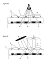
- the rotational misalignment or the small pitch mismatch results in the eye observing a different part of the image in each neighbouring lens resulting in a magnified image 15, illustrated in Figure 2 for the case of rotational misalignment. If the eye is then moved relative to the lens/image array a different part of the image is observed giving the impression that the image is in a different position. If the eye is moved in a smooth manner a series of images are observed giving rise to the impression that the image is moving relative to the surface. In the case where the pitch mismatch is generated by rotational misalignment the array of magnified images is rotated relative to the microimage array and consequently the parallax affect that results in the apparent movement of the magnified image is also rotated and this is known as skew parallax.
- the nature of the movement and orientation changes can be explained from the theory of moiré; this is discussed in detail in " The theory of the Moire phenomenon” by I. Amidror published by Kluiver Academic Publishers in 2000, ISBN 0-7923-5949-6 .
- the moiré effect of two periodic structures can be explained/predicted by considering the frequency vectors of the two structures.
- the orientation of the frequency vector represents the direction of the periodicity and the length represents the frequency (i.e. 1/Period).
- the vector is expressed by its Cartesian coordinates (u,v) where u and v are the horizontal and vertical components of the frequency.
- a one-dimensional grating is represented by a pair of points in the frequency plane (strictly, the grating should be a sinusoid to only have two points in the frequency plane).
- the representation of two one-dimensional gratings, with the same frequency but different orientation as frequency vectors, is shown in Figure 3 .
- Grating 1 can be represented by the two points f 1 and -f 1
- grating 2 can be represented by the two points f 2 and -f 2 .
- the spectrum produced from the convolution of the two frequency representations (grating 3) indicates what moiré frequencies will occur. To be visible, the moiré must be close to the origin (i.e.
- a large magnification corresponds to a low frequency moiré. It can be seen from the frequency representation in Figure 3 that a low frequency moiré requires a close match of frequency and orientation. It can also be seen in Figure 3 that the resultant moiré frequency vector is at -90° to the individual frequency vectors. If instead of two one-dimensional gratings we have a superposition of a microlens array and a microimage array then the resultant moiré frequency vector corresponds to the magnified image array which will be orientated at ⁇ 90° to the microlens and microimage arrays. The degree of magnification is dependent on the ratio of the frequency of the microimage over the frequency of the magnified (moiré) image, i.e: f microimage/ f moire .
- US 5712731 discloses the use of the microlens array as a separate device for viewing the associated microimage or as one fully bonded device. However it is not possible to produce microimages at a sufficiently small scale to create a thin ( ⁇ 50 ⁇ m) fully bonded flexible device using the printing or embossing techniques disclosed in US 5712731 .
- the images are constructed by using light traps to create the black pixels.
- the light traps comprise reflective tapered structures with relatively high aspect ratios. Light entering the tapered structure is reflected and approximately 10% of the light may be absorbed. Due to the morphology of the structures the light is reflected many times and in this way all of the light is absorbed by the structure before it has the chance to exit the light trap.
- the light traps are formed during reactive ion etching of a layer of photopolymer and are a result of impurities/inclusions in the composition of the photopolymer.
- a master is then generated using conventional photolithographic techniques and the structure is then replicated into a polymer film. This technique allows the creation of black pixels at the limit of optical detection with a resolution of up to 100000dpi. Arrays of microimages generated from such very fine pixels can be combined with microlenses to form thin flexible security devices of ⁇ 50 ⁇ m producing autostereoscopic and dynamic images.
- a high-resolution colour image can be created by overprinting the high-resolution black and white image with a transparent lower resolution colour image.
- the light traps allow the formation of very high resolution identifying images there are a number of processing issues associated with them.
- the light traps are formed during reactive ion etching as a result of impurities or inclusions in a photopolymer. Therefore the exact structure of each light trap cannot be specified and is not reproducible which could lead to variability in the final image.
- Once the structures are formed and a master produced the structure must be copied with very high fidelity into polymeric film using a replication process suitable for mass production.
- the high aspect ratio of the light trap structures ( ⁇ 1:5) can result in difficulties in replicating these structures in polymeric films. It is known that the fidelity of replicated nanoscale and microscale structures is very dependent on the aspect ratio. In "Micro-optics.
- EP-A-0238043 describes a document having an embedded security thread.
- the security thread is transparent and has a printed pattern on one side and, on the opposite side, a lenticular structure coordinated with the printed pattern. Such threads change their appearance when the viewing angle changes.
- a transparent film impressed with the desired lenticular relief is directed to a printing apparatus in exact register via guide elements having a relief structure that is negative with respect to the film impression, and then divided in a cutting apparatus into individual threads.
- a security device comprises a substrate having an array of microlenses on one side and one or more corresponding arrays of microimages on the other side, the microimages being located at a distance from the microlenses substantially equal to the focal length of the microlenses, the substrate being sufficiently transparent to enable light to pass through the microlenses so as to reach the microimages and is characterized in that each microimage is defined by an anti-reflection structure on the substrate formed by a periodic array of identical structural elements and an at least partially reflecting layer on the same side of the substrate as the anti-reflection structure, the anti-reflection structure reducing the reflective property of the reflecting layer, wherein one or both of the anti-reflection structure and the at least partially reflecting layer is in the shape of a microimage, whereby light passing through the substrate and impinging on the microimages is reflected to a different extent than light which does not impinge on the microimages thereby rendering the microimages visible.
- a method of manufacturing a security device comprises providing an array of microlenses on one side of a substrate and one or more corresponding arrays of microimages on the other side, the microimages being located at a distance from the microlenses substantially equal to the focal length of the microlenses, the substrate being sufficiently transparent to enable light to pass through the microlenses so as to reach the microimages and is characterized in that each microimage is defined by an anti-reflection structure on the substrate formed by a periodic array of identical structural elements, and an at least partially reflecting layer on the same side of the substrate as the anti-reflection structure, the anti-reflection structure reducing the reflective property of the reflecting layer, wherein one or both of the anti-reflection structure and the at least partially reflecting layer is in the shape of a microimage, whereby light passing through the substrate and impinging on the microimages is reflected to a different extent than light which does not impinge on the microimages thereby rendering the microimages
- the first and second aspects of the invention provide an alternative solution for the manufacture of thin optically variable security devices utilising non-holographic micro-optical structures.
- a new security device is disclosed which combines a microlens and microimage array, on two opposing surfaces of a substrate, typically polymeric film, to form an optically variable device in which a thin structure is achieved by creating high resolution images.
- the microimage and microlens array can be formed on separate polymeric films, which are subsequently laminated together to generate the optically variable device.
- the optically variable device of the current invention is based on the interaction between an analysing array of microlenses and a corresponding set of identical microimages, as described in US 5712731 .
- each lens has underneath it a microimage in perfect register so that an observer sees only one magnified image of the microimages.
- introducing a pitch mismatch between the microlens array and the microimage array splits the single magnified image into a regular array of images with the number of visible images increasing and their individual sizes decreasing as the pitch mismatch increases.
- the area and unit length over which the lenses and images are substantially in phase to form a visible picture decreases so that the device ceases to display a single image and starts to display an array of much smaller regular images which show the loss of perfect register between the lenses and the microimages.
- the overlap image areas are essentially determined by the moiré pattern formed between the lens and image arrays and so particular versions of this type of device have been termed the "moiré magnifier".
- the pitch mismatch can be achieved by simply varying the pitch or preferably by introducing a rotational misalignment between the microimage and microlens array.
- the microimage array is not produced by a printing technique but instead from the optical properties of a, preferably metallised, anti-reflection microstructure.
- Anti-reflection structures are well known in the field of optics and designed to reduce reflections arising from abrupt changes in the refractive index at the interface of two materials.
- a periodic array of surface structures that are smaller than the wavelength of light provides a continuous transition of the refractive index rather than an abrupt change, and reflection is minimised.
- a typical application for such a structure would be as an anti-glare film in flat panel displays.
- One particular type of submicron anti-reflection structure is known as a moth-eye structure.
- the moth-eye structure has a repeating period typically in the range 200-400nm and a height typically in the range 250-350nm.
- Anti-reflection microstructures typically two-dimensional although one-dimensional structures are also envisaged, including those mimicking the moth-eye structure, can be produced using conventional replication technologies. Holographic exposure can be used to produce a master, which is then used to create a metal tool containing the negative image. The metal tool is then used to replicate the structure in a polymeric film using either a batch or roll-to-roll process.
- the present invention utilizes the fact that periodic anti-reflection structures appear black when metallised. This was described in " Artificial Media Optical Properties - Subwavelength Scale” published in the Encyclopaedia of Optical Engineering (ISBN 0-8247-4258-3), 09/03/2003, pages 62-71 . This property enables the creation of high-resolution images using conventional replication and metallising technologies. In one example an anti-reflection structure would be replicated in a polymer film in the form of an identifying image.
- the identifying image On metallising the polymer film the identifying image would appear black as a result of the anti-reflection structures and the non-image, plain metal areas, would appear bright.
- the resolution of the images will depend on the period of the anti-reflection structure.
- a moth-eye structured film with a period of 250nm is available commercially from Autotype and Wavefront Technology Inc, and this would allow a minimum pixel size of 250nm, which equates to a resolution of 100,000dpi.
- An improvement over the prior art is that the identifying images can be replicated in a more straightforward and controlled manner due to the low aspect ratio of the anti-reflection structures.
- the commercially available moth eye structure typically has an aspect ratio in the range 1:0.8 - 1:2 compared to the much higher aspect ratio of the light traps, ⁇ 1:5, described in the prior art.
- a further improvement over the prior art is that the master anti-reflection structures are created in a lacquer or photoresist using known holographic or diffraction grating techniques, which allows precise control over the origination of the final high resolution image. As it is a periodic microstructure each pixel is created by an identical microstructure. This contrasts with the light traps, detailed in the prior art, which are formed during reactive ion etching as a result of impurities or inclusions in a photopolymer. The exact structure of each light trap cannot be specified and is not reproducible which could lead to variability in the final image.
- the incorporation of demetallised indicia in the.metallised surface containing the microimage array can further improve the anti-counterfeit nature of the device.
- This combines the advantages of the optically variable effects generated using a thin moiré magnifier with the advantages of indicia formed from demetallisation.
- demetallised indicia such as described in EP 0279880 and EP 319157 has proved to be highly effective in reducing counterfeiting.
- a further advantage of the moth-eye anti-reflection structure is that it has a reduced wettability created by a combination of structure and surface energy. This means that an applied liquid will not wet out the surface and will tend to roll off the surface due to insufficient surface tension to hold it in place.
- This property can be used to create preferential removal of Al on the metallised surface containing the microimage array by contact with a caustic solution of NaOH in water. The caustic solution will wet the non-image plain metal areas but will not wet the metallised moth-eye structure, which forms the identifying image. Under these conditions, the plain areas would then become transparent after demetallisation whilst the moth-eye areas would remain black.
- the formation of a high contrast, high-resolution black/transparent image enables the thin moiré magnifier device to be used in transmission as well as reflection.
- the security device of the current invention can be used to authenticate a variety of substrates but is particularly suitable for application to flexible substrates such as paper and in particular banknotes (where the device could define a patch or a thread).
- the thickness of the security device depends on how it is employed within the banknote. For example as a patch applied to a banknote the desired thickness will range from a few microns for a hot stamped patch up to ⁇ 50 ⁇ m for label applications. In the case of a windowed security thread the security device would typically have a final thickness in the range 20-50 ⁇ m. Thicker versions of the security device (up to 300 ⁇ m) could be employed in applications which include passport paper pages, plastic passport covers, visas, identity cards, brand identification labels, anti-tamper labels--any visually authenticable items.
- FIG. 4 there is illustrated a cross-section of a substrate typical of the construction of the present invention for use in security or authenticating devices.
- the construction comprises a substantially clear polymeric film 1 of polyethylene terephthalate (PET) .
- PET polyethylene terephthalate
- On one surface 2 of the polymeric film is an array of microlenses 3.
- Microimages 4 in the form of anti-reflection structures are formed in the opposite surface.
- a thin metallic layer 5 is then applied to the surface containing the microimages in both the image and non-image areas.
- the clear polymeric film 1 acts as an optical spacer layer and its thickness is such that the microimages 4 are situated at the focal plane of the microlenses 3.
- the preferred method of the current invention is to have a microlens and microimage array with substantially the same pitch where the pitch mismatch is achieved by introducing a small rotational misalignment between the microimage and microlens array.
- the degree of rotational misalignment between the microimage and microlens array is preferably in the range 15° - 0.05°, which results in a magnification range of between ⁇ 4X-1000X for the microimage array. More preferably the rotational misalignment is in the range 2° - 0.1°, which results in a magnification range of between ⁇ 25X-500X for the microimage array.
- the microimage array and microlens array are in substantially perfect rotational alignment but with a small pitch mismatch.
- a small pitch mismatch would equate to a percentage increase/decrease of the pitch of the microimage array relative to the microlens array in the range 25% - 0.1 %, which results in a magnification range of between ⁇ 4X-1000X for the microimage array.
- the percentage increase/decrease of the pitch of the microimage array relative to the microlens array is in the range 4% - 0.2%, which results in a magnification range of between ⁇ 25X-500X for the microimage arrays.
- microlens array will be described in section 1, followed by a description of the anti-reflection image forming structures in section 2, the device construction in section 3, the incorporation of the device within a security document in section 4, and the improved optically variable characteristics of the security device in section 5.
- FIG. 5 is a small section of the construction in Figure 4 , showing a single plano-convex microlens 3 on one surface of the clear polymeric film 1, and a single microimage 4 comprising an anti-reflection structure on the opposite surface.
- the thickness, t, of the clear polymeric film 1 is substantially equal to the back focal length, f, of the microlens 3 in the clear polymeric film.
- the present invention is not limited to any specific type or geometry of microlens, the only requirement being that the microlens can be used to form an image.
- Microlenses suitable for the present invention include those that refract light at a suitably curved surface of a homogenous material such as plano-convex lenslets, double convex lenslets, and fresnel lenses.
- the present invention will comprise spherical microlenses but lenses of any symmetry including cylindrical lenses could be employed. Both spherical and aspherical surfaces are applicable to the present invention. It is not essential for the microlenses to have a curved surface.
- Gradient refractive index (GRIN) lenses image light by a gradual refraction throughout the bulk of the material as a result of small variations in refractive index.
- Microlenses, based on diffraction, such as Fresnel zone plates can also be used.
- GRIN lenses and amplitude or mask based fresnel zone plates enable the surface containing the microlens array to be planar and offers advantage in print receptivity and durability.
- microlens array could comprise discrete lenslets such as microspheres, rods, beads or cylinders, it is preferable to use a periodic array of lenses generated by a replication process.
- Master microlens arrays can be produced by number of techniques such as photothermal techniques, melt and reflow of photoresist and photoresist sculpture. Such techniques are known to those skilled in the art and are detailed in chapter 5 of "Micro-Optics: Elements, Systems, and Applications” edited by Hans Peter Herzig, published by Taylor and Francis, reprinted 1998 .
- the master microlens structure can then be physically copied by commercially available replication techniques such as hot embossing, moulding or casting.
- microlens structures can be replicated include but are not limited to thermoplastic polymers such as polycarbonate and polymethylmethacrylate (PMMA) forthe hot embossing and moulding processes and acrylated epoxy materials curable by heat or radiation for the casting process.
- thermoplastic polymers such as polycarbonate and polymethylmethacrylate (PMMA) forthe hot embossing and moulding processes and acrylated epoxy materials curable by heat or radiation for the casting process.
- PMMA polymethylmethacrylate
- the microlens array is replicated via casting into a UV curable coating applied to a carrier polymer film such as PET.
- the thickness of the present invention is dependent on the key characteristics of the microlenses, which are the focal length and the lens diameter, D. If we approximate the lens to a spherical (non-aspheric) thin lens then the focal length is effectively equivalent to the back focal length, f.
- the f-number, f/#, of a lens is defined as f/D. We can calculate the limit on the f/#:
- the thickness, t, of the clear polymeric film would need to be in the range 1-50 ⁇ m and more preferably in the range 10-30 ⁇ m.
- the back focal length of the microlenses must substantially be in the same range.
- the diameter, D, of the microlenses would fall in the range 1-50 ⁇ m and more preferably in the range 10-30 ⁇ m for application in a thin flexible security device.
- the back focal length could be decreased by decreasing the refractive index of the clear polymeric film or increasing the refractive index of the microlenses.
- the present invention utilises the combination of a microimage array with a microlens array to generate magnified images, which exhibit optically variable effects such as visually distinct movement and apparent depth.
- the thickness of the device is dependent on the back focal length of the microlenses, which is in turn a function of the diameter of the individual lenses.
- lens diameters within the range 1-50 ⁇ m would be appropriate.
- the microimage array In order for the device to function optimally the microimage array must have substantially the same pitch as the microlens array. Therefore a key challenge to producing a thin, flexible device is the generation of high-resolution high contrast images.
- the characteristics of the microimage layer of the present invention are key to producing such a thin device in a cost efficient and reproducible manner and differentiate the present invention from the prior art.
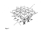
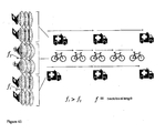
- Figure 7 illustrates the cooperation between the microlens array and the microimage array.
- an array 7 of microimages of the object A is viewed through an array 8 of microlenses.
- a typical microimage array 7 will comprise many (e.g. 100 or more) microimage elements, repeating many times in each direction with a regular pitch.
- the lens diameter, D, of the microlens array 7 and therefore the pitch, because there is no spacing between the lenses, is 30 ⁇ m.
- the fact that the microlens array 7 and the microimage array 8 must have substantially the same pitch dictates that the microimage must be created within a 30 ⁇ m x 30 ⁇ m square area or less as it is preferable to leave a gap between the microimages.
- a pixel size of 1 ⁇ m creates an image array containing 900 pixels that allows the formation of identifying images such as letters and numerals. If the pixel size is reduced further to 0.5 ⁇ m, more complicated identifying images could be generated from the 3600 pixel array.
- the preferred embodiments of the current invention utilise the fact that periodic submicron anti-reflection structures appear black when metallised. It is therefore possible to write an image on the surface of a polymeric film in the form of a sub-micron anti-reflection structure. On metallising the film a high degree of contrast is generated between the image area, comprising the anti-reflection structure, which will appear black and the non-image areas, which will have a bright metallic appearance.
- An anti-reflection structure of the type utilised in the current invention is any periodic structure that is finer than the wavelength of light and provides a surface layer in which the refractive index varies gradually from unity to the index of the bulk material, and thereby minimises reflections that are associated with sudden changes in refractive index.
- moth-eye structure which is commercially available from a number of companies including Autotype International under the tradename MARAG TM .
- MARAG TM sub-micron periodic anti-reflection structure
- These commercially produced films mimic the structure observed on the eye of some nocturnal moths that minimises the reflection of light allowing the moths to remain undetected by predators.
- Moth-eye films have a characteristic "egg box" periodic modulation typically with a repeating period in the range 200-400nm and a structure height in the range 250-350nm.
- the reflectance is expected to be very low for wavelengths of light ⁇ 2.5h and greater than d at normal incidence, and for wavelengths >2d for oblique incidence, based on information in US 6570710 filed in the name of Reflexite Corporation. If the visible part of the electromagnetic spectrum is considered in the range 400-700nm then the reflectance would be very low in the visible region of the electromagnetic spectrum for a structure with a height of ⁇ 280nm and a period of 200nm. This structure would have an aspect ratio of 1:1.4, which is significantly lower and therefore easier to process than the light trap structures described in the prior art in US 5503902 .
- the anti-reflection moth-eye structures can be produced on a photoresist-covered glass substrate by a holographic exposure using an ultraviolet laser. This process is disclosed in US 4013465 filed in the name of Clapham and Hutley.
- the moth-eye structures can be made one-dimensional or two-dimensional, as discussed in patent US 6570710 .
- the two-dimensional moth-eye structures are used for the embodiments discussed in this disclosure but the invention could equally well be constructed using the one-dimensional structures.
- the first step ( Figure 8a ) is to produce a master structure 19 in a photopolymer layer 20 on a support 21 that comprises the moth-eye anti-reflection structure 23 in the form of a microimage array 22.
- Techniques for creating the moth-eye anti-reflection structure in the form of a microimage include holographic exposure, photolithography, laser writing and e-beam technologies.
- Figure 8b illustrates one of the identifying microimages 25 showing the individual moth-eye anti-reflection structural elements 26.
- FIG. 9a illustrates a standard electroforming process, illustrated in cross-section in Figure 9a .
- the microimage structure in the Ni shim 27 is then copied on the surface of a polymeric film 28 using standard replication processes ( Figure 9b ).
- Such processes include hot embossing, UV casting and moulding.
- the preferred replication processes for the current invention are hot embossing or UV casting as both allow continuous roll-to-roll production, which is important for mass production of the device in a cost efficient manner.
- Figure 9b illustrates the UV casting replication process in which a thin layer of a UV curable polymer 29 is coated onto the clear polymeric film 28, which is then pressed against the Ni shim 27.
- the UV curable polymer is then cured before being separated from the Ni shim leaving the microimage structure replicated into the UV curable polymeric layer 29 on the surface of the clear polymeric film 28.
- One of the replicated microimages 30 is illustrated in Figure 10a .
- the moth-eye anti-reflection structure in the form of identifying microimage 30 appears black in contrast to the non-structured areas of the film, which appear metallic.
- the identifying microimage effectively consists of black pixels that are ⁇ 0.25 ⁇ m in diameter correlating to an optimum resolution of ⁇ 100000dpi.
- the thin metallic layer 40 is preferably produced using vacuum deposition.
- the final replicated microimage array is illustrated in Figure 10c with black microimages against a bright metallic background.
- the thin metallic layer can be applied only over the moth-eye anti-reflection structures. In this case, the device will consist of black microimages against a transparent background.
- a pixel size of 0.25 ⁇ m means that a metallised moth-eye anti-reflection structure can be used to create a complex micro-image in a 30 ⁇ m x 30 ⁇ m square area containing up to 14400 pixels (120x120 pixel array). This very high level of resolution enables the creation of a thin moiré magnifier suitable for application on flexible documents such as banknotes.
- microimage array illustrated in Figure 10 with black microimages against a bright metallic background would when combined with an appropriate microlens array produce a device operating in reflection, as illustrated in Figure 4 .
- One method for obtaining a microimage array suitable for operation in transmission mode is illustrated in Figure 11 .
- the method is the same as that illustrated in Figures 8-10a except that the motheye anti-reflection structure 45 is no longer restricted to defined image areas and covers the whole of the UV curable polymeric layer 29, shown in Figure 11 a.
- the individual microimages 47 are then formed by selectively metallising the moth-eye anti-reflection structure, illustrated in Figure 11 b.
- microimages In transmission the microimages would appear black on a cleartransparent background.
- Conventional metallisation techniques such as vacuum deposition cannot achieve the very high resolution required for selective metallisation of microimages in the range 1-50 ⁇ m and therefore are not suitable for creating thin flexible devices.
- High-resolution selective metallisation can be achieved using techniques such as soft lithography as developed by IBM and detailed in the IBM Journal of Research and Development, volume 45, number 5, 2001 .
- the high contrast image structures described above do not have to be achieved by metallising the moth-eye anti-reflection structures, alternative methods may be used but reflecting properties are required.
- a transparent reflection-enhancing layer instead of a metallic layer
- the anti-reflection moth-eye will negate the effect of the reflection-enhancing layer so incident light will be transmitted in that region.
- the film In the non-structured regions the film will be transparent but with a significant amount of reflection. Having regions of reflective and non-reflective film generates the image contrast.
- An example of a suitable refection enhancing material is zinc sulphide, which can be vacuum deposited to form a transparent thin layer.
- an additional absorptive layer can be used.
- the absorptive layer is preferably applied over both the non-structured areas and the moth-eye anti-reflection structures. Examples of the type of suitable absorptive materials include dyed or pigmented inks and coatings.
- absorptive layer can be any colour.
- the colour would be provided by a dyed or pigmented ink. The colour would not have to be the same all over the device; multiple colours are possible in different regions.
- Colour generation is also possible with the embodiments comprising the metallised moth-eye anti-reflection structures.
- the reflectance is very low for wavelengths below ⁇ 2.5x the height of the moth-eye anti-reflection structure and for wavelengths greater than the period of the moth-eye anti-reflection structure (at normal incidence). So by using a structure height too short to reflect all the visible spectrum (-200-250nm say) wavelengths of >500-625nm will be reflected giving a red appearance to the moth-eye anti-reflection structure. Similarly, by using a period too long for all wavelengths to be reflected ( ⁇ 500nm say) the moth-eye anti-reflection structure will have a blue appearance (at normal incidence). The colour seen will change in intensity and hue with angle.
- microlenses and the high-resolution microimage arrays described in the sections above must now be combined to provide a thin optically variable device.
- the device must be constructed such that the back focal length of the lenses is substantially equal to the separation between the microlens and microimage arrays in order that the lenses image the microimages.
- Figure 4 illustrates a typical device construction of the current invention in which the device comprises a single layer, clear polymeric film.
- Preferred materials forthe clear polymeric film include PET, polyamide, polycarbonate, poly(vinylchloride) (PVC), poly(vinylidenechloride)(PVdC), polymethylmethacrylate (PMMA), polyethylene naphthalate and polypropylene.
- PVC poly(vinylchloride)
- PVdC poly(vinylidenechloride)
- PMMA polymethylmethacrylate
- the microlens array is replicated to one surface of the film and the corresponding microimage array is replicated to the opposite surface.
- FIG. 12 A schematic of a method for producing a device of the current invention comprising a single layer film ( Figure 4 ) is shown in Figure 12 .
- the microlens array and the microimage array are replicated into the polymeric film in different process steps in a continuous roll-to-roll process.
- a roll of clear polymeric film of PET is coated 50 on its first surface with a layer of UV curable polymer.
- Suitable UV curable polymers include photopolymer NOA61 available from Norland Products. Inc, New Jersey.
- the film is then brought into contact 52 with the first embossing roller that contains the negative of a master structure for the microlens array.
- the microlens array structure is replicated in the UV curable polymer layer.
- the UV curable polymer layer is cured 54 by application of UV radiation and the coated film is then released form the embossing roller.
- a layer of UV curable polymer such as NOA61 is then coated 56 onto the opposite second surface of the film.
- the second surface of the film is then brought into contact 58A with the second embossing roller that contains the negative of a master structure for the anti-reflection moth-eye structure.
- the moth-eye anti-reflection structure is replicated in the UV curable polymer layer on the second surface of the clear polymeric film.
- the UV curable polymer layer is cured 60A by application of UV radiation and the coated film is then released from the embossing roller.
- the moth-eye anti-reflection structure takes the form of the microimage array (step 58A).
- a thin metallic layer is then applied (62A) to the second surface of the polymeric film.
- a suitable thin metallic layer would be Al applied by vacuum deposition.
- the thin metallic layer is preferably applied uniformly (62A) over the whole active area of the second surface of the polymer film.
- a transmissive device can be produced by replacing the thin metallic layer with a suitable reflection enhancing material, for example zinc sulphide, which can be applied to form a transparent thin layer.
- a transmissive device can be generated by following process route B in Figure 12 . The process differs for the transmissive device from stage 58 onwards.
- the moth-eye anti-reflection structure is replicated uniformly over the whole active area of the second surface of the polymer film (58B). Once the structure is replicated the UV curable polymer layer is cured (60B) by application of UV radiation and the coated film is then released from the embossing roller.
- a thin metallic layer is then selectively applied (62B) to the moth-eye anti-reflection structures in order to form the identifying microimage array.
- microlens array structure and the microimage array structure could be replicated onto opposite surfaces of the polymeric film simultaneously. Such a method would facilitate the control of the registration between the microlens and microimage arrays.
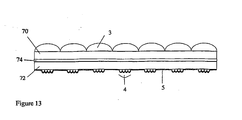
- FIG. 13 illustrates an example of a laminate construction for the current invention.
- the microlens array 3 is replicated in one surface of the first clear polymeric film 70 and the corresponding microimage array 4 is replicated in one surface of the second clear polymeric film 72.
- a layer of suitable adhesive 74 may be required, for this process, applied between the non-structured surfaces of the clear polymeric films.
- the registration of the microimage array to the microlens array must be controlled.
- the degree of register between the two arrays depends on the required optical properties of the security device. This is discussed in detail in EP 0698256 filed in the name of De La Rue International.
- the pitches of the microimage array and the microlens array are identical and the two are accurately aligned and the microimages are near the focal planes of the microimages. When this system is viewed from a given direction each microlens images the corresponding point on the image underneath it to form a single highly magnified image of the underlying microimage element.
- a pitch mismatch between the microlens array and the microimage array is generated by angularly misaligning the arrays.
- the rotational misalignment between the two arrays results in the single magnified image splitting into a regular array of images with the number of visible images increasing and their individual sizes decreasing as the angular mismatch increases.
- much looser register/alignment constraints are required to form a viewable image, although it is still necessary to control the degree of registration such that the magnified image falls within defined tolerances.
- a further device construction is one in which the microlens array comprises gradient refractive index lenses as illustrated in Figure 14 .
- Gradient refractive index (GRIN) lenses image light by a gradual refraction throughout the bulk of the material as a result of small variations in refractive index.
- GRIN lenses can be formed in a layer of photopolymer using a number of known techniques for example in US 5442482 microlenses in the form of GRIN lenses may be formed by selective exposure of a photopolymer to a pattern of dots, such exposure being in ultra-violet light or suitable visible light and being effected by "contact" exposure through a mask having an array of circular holes formed therein, or by spot-by-spot exposure using a scanned ultra-violet laser, or by ultra-violet holography.
- the photopolymer can then be used to produce a nickel master enabling the structure to be replicated into a photopolymer layer applied to a carrier polymer film such as PET.
- GRIN lenses can be formed in polymer materials by diffusion polymerisation as detailed in chapter 5 of "Micro-Optics: Elements, Systems, and Applications” edited by Hans Peter Herzig.
- the advantage of using GRIN lenses to form the microlens array of the current invention is that it enables the surface of the microlens array to be planar which facilitates overcoating or overprinting the device with further protective coatings or printed layers.
- the example device construction in Figure 14 operates in reflective mode and comprises a GRIN microlens array 80 in the form of a photopolymer film that is adhered to the first surface of a clear polymeric film 82.
- a moth-eye anti-reflection structure is replicated in the second surface of the clear polymeric film to form an identifying microimage array 4.
- a thin metallic layer 5 is applied over the microimage array and the non-imaged sections of the second surface of the clear polymeric film.
- the device illustrated in Figure 14 can be made to operate in transmission by replicating the moth-eye anti-reflection structure over the whole active area of the second surface of the clear polymeric film and then selectively metallising only the moth-eye anti-reflection structures which are used to form the identifying images.
- FIG. 15 A further device construction of the current invention is illustrated in Figure 15 in which a holographic structure 86 is incorporated into the top surface of the microlenses 3.
- the zero order (non-diffracted) rays 88 are transmitted undeflected by the hologram and will be focussed onto the microimage 4 and will be used to form the magnified image of the microimages as described in the previous embodiments.
- the incoming rays that undergo first order diffraction from the holographic structure forms a holographic image 89.
- a reflection enhancing layer may be applied to the holographic structure (such as described in U.S. Pat. No. 4,856,857 ).
- the device illustrated in Figure 15 would be constructed such that for a certain set of viewing angles the magnified array of microimages would be visible while the brightness of the holographic image would be significantly reduced, but at a different viewing angles the increased brightness of the holographic image would make it clearly visible while the magnified array of microimage would have significantly reduced visibility. A switch between the magnified microimage and the holographic image is therefore observed on tilting the device.
- FIG. 16a and 16b A further device construction of the present invention is illustrated in Figures 16a and 16b in which an opaque mask 90 is deposited around the edges of the individual microlenses 3.
- Preferred materials for the masking 90 include a thin coating of Al applied using standard vacuum deposition techniques.
- the mask 90 could be created by selectively metallising each microlens 3 or metallising the whole surface of each microlens and then selectively demetallising to create an aperture 92 in the top of the lens.
- non-perfect registration between the microlens array 3 and the microimage array 4 for e.g.
- the array of magnified images will move on tilting and the shadowing effect of the opaque mask will cause a variation in brightness with certain areas of the microimage array being illuminated and other areas being shaded depending on the lighting conditions.
- the observer will see a bright image 98 when viewed normally to the surface of the clear polymeric film 1 and a dark image 99 when viewed off-axis, such that the image appears to fade in and out of view on tilting as shown in Figure 16b .
- the various embodiments of the device construction described above can be slit or cut into patches, foils, stripes, strips or threads for incorporation into plastic or paper substrates in accordance with known methods.
- the current invention could be incorporated into a security paper as a windowed thread.
- a security thread 100 formed by a device according to the invention with windows of exposed thread 102 and areas of embedded thread 104 in a document 105.
- EP 860298 and WO 03095188 describe different approaches for the embedding of wider threads into a paper substrate. Wide threads are particularly useful as the additional exposed area allows for better use of optically variable devices such as the current invention.
- Figure 18a illustrates an example cross-section of a security thread suitable for use as a windowed thread in paper, in which the device construction illustrated in Figure 4 has been modified by the application of a layer of transparent colourless adhesive 107 to the outer surface containing the microlens array and the application of a layer of adhesive 108 to the outer surface containing the microimage array.
- Careful selection of the optical properties of the adhesive in contact with the microlenses is important.
- the adhesive must have a lower refractive index than the microlens material and the greater the difference in the refractive index between the microlenses and the adhesive the shorter the back focal length of the lenses and therefore the thinner the final security device.
- demetallised indicia in security threads is well known and is described in EP 0319157 .
- the highly advantageous characteristics of demetallised indicia are combined with the optical variable effects created by the combination of the microlens and microimage arrays.
- the thin metallic layer 5 is demetallised such that metal free regions 110 are formed which overlap the image and non-image areas.
- demetallisation destroys the contrast between the image and non-image areas.
- a further advantage of the moth-eye anti-reflection structure is that it has a reduced wettability created by a combination of structure and surface energy. An applied liquid will not wet out the surface and will tend to roll off the surface due to insufficient surface tension to hold it in place.
- This property can be used to create preferential removal of Al by contact with a caustic solution of NaOH in water.
- the caustic solution will wet the non-image plain metal areas but will not wet the metallised moth-eye anti-reflection structure, which forms the identifying image. Under these conditions, the plain areas would then become transparent after demetallisation whilst the moth-eye areas would remain black.
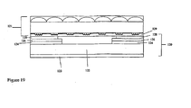
- Figure 19 shows a machine readable construction 120 laminated to the basic construction 121 illustrated in Figure 18a .
- the machine-readable construction comprises a polymeric film 122, such as a metallised 12 ⁇ m PET base coated with an adhesive 123 on the non-metallised side, which has been selectively demetallised.
- a polymeric film 122 such as a metallised 12 ⁇ m PET base coated with an adhesive 123 on the non-metallised side, which has been selectively demetallised.
- two "tramlines” of metal 124 have been left along each edge of the construction but other variants are possible as illustrated within the cited prior art.
- The"tramlines” 124 are such that when the final construction is laminated to substrate they are coincident with only metallised regions.
- a protective layer 126 may be applied onto the"tramlines" to prevent the metal being corroded by the magnetic layer 128, which is applied next.
- a suitable protective layer 126 is VHL31534 supplied by Sun Chemical applied with coat weight of 2gsm.
- a suitable magnetic material is FX 1021 supplied by Ferron applied with a coat weight of 2-6 gsm.
- a suitable laminating adhesive 129 is applied. The whole construction is then laminated to the basic structure illustrated in Figure 18a to form the final machine-readable device.
- the current invention could be incorporated into a security document 130 as a security patch 132 or stripe 134. This is illustrated in Figure 20 showing a security patch 132 and a security stripe 134 exhibiting a magnified image 135 resulting from the construction of the present invention.
- Figure 21 illustrates an example cross-section of a security patch or foil, in which the device construction illustrated in Figure 4 has been modified by the application of a heat or pressure sensitive adhesive 136 to the outer surface containing the microimage array.
- an optional protective coating/varnish 138 has been applied to the outer surface containing the microlens array 3.
- the function of the protective coating/varnish 138 is to increase the durability of the foil/stripe both during transfer onto the security substrate and in circulation.
- the protective coating must have a significantly lower refractive index than the refractive index of the microlenses for the same reasons that were discussed for the security thread adhesive.
- the device illustrated in Figure 21 can be transferred to a security document 130 by a number of known methods including hot stamping and the method described in US 5248544 .
- the outer adhesive coating on the security thread and the protective coating on the patch/stripe can be overprinted using standard banknote printing techniques such as lithography and intaglio.
- standard banknote printing techniques such as lithography and intaglio.
- coloured transparent inks enables the magnified microimages to be of a defined colour.
- the device of the current invention can be integrated into documents where the substrate is a transparent polymeric film.
- An example of this type of document would be polymer banknotes, particularly those described in WO 8300659 , in which a transparent substrate is coated on both sides with layers of an opacifying material.
- the opaque layer 140 is applied in such a way as to leave a transparent region 142 for inspection of a security device.
- microimages 4 in the form of moth-eye anti-reflection structures are replicated onto one surface of the transparent region 142 of the polymer banknote substrate 144 and the corresponding microlens array 3 could be replicated onto the opposite surface.
- a thin metallic layer 5 is then applied over the image and non-image regions of the surface of the transparent region 142 containing the microimage array 4.
- the transparent polymer substrate is used as the optical spacer to allow the image recorded in the microimage array to be recognisable through the microlens array. On viewing the device, from the top of the document, the magnified microimages will appear black on a metallic background.
- the reflective device in Figure 22 can be replaced with a device that operates in transmission. This can be achieved by replacing the thin metallic layer 5 with a suitable reflection enhancing material, for example zinc sulphide, which can be applied to form a transparent thin layer. On viewing the device, from the top of the document, the magnified microimages will appear non-reflective against a highly reflective glossy background.
- a suitable reflection enhancing material for example zinc sulphide
- a transmissive device can be generated by replicating the moth-eye anti-reflection structures 146 uniformly over the transparent region 142.
- a thin metallic layer 5 is then selectively applied to the anti-reflection structures in order to form the identifying microimage array.
- the magnified microimages will appear black against a transparent background.
- a further aspect of the device of the current invention operating in transmission is that the magnified array is only clearly discernible when viewed from the side of the document with the microlens array.
- a further application of a transmissive device would be in the transparent aperture 150 of a paper banknote 152 such as those described in EP 1141480 .
- This process enables a wide strip of an impermeable substrate to be included in a paper substrate.
- Figure 24 illustrates an example of such a paper substrate 152 into which an impermeable strip 154 is incorporated to create an aperture 150.
- both surfaces of the impermeable substrate are visible, however the remainder of the strip is only visible from one side of the document as shown in Figure 24a and not from the reverse side where the impermeable strip is covered by paper fibres as shown in Figure 24b .
- Figure 25 shows a cross-section of one embodiment of the current invention that could be incorporated into a banknote as an aperture in the form of impermeable strip in Figure 24 .
- the device construction is as illustrated in Figure 4 except that the anti-reflection moth-eye structure is no longer restricted to defined image areas and covers the whole of surface of the clear polymeric film 1.
- the individual microimages are then formed by selectively metallising 5 the moth-eye anti-reflection structures 146.
- an adhesive 160 is applied to the outer surface containing the microimage array.
- the optically variable device covers the whole surface of the impermeable strip, and is inserted such that the microlens array is on the upper surface as viewed in Figure 24a , then from the side of the document shown in Figure 24a the magnified image will be viewable in reflection in area (A) and transmission and reflection in area (B). From the reverse side of the document ( Figure 24b ) it will only be visible in area B and not very clearly discernible because the microimages are not being viewed directly through the microlens array.
- a reflective device can be included as an aperture in a paper banknote.
- a typical device construction is shown in Figure 26 .
- the device construction is as illustrated in Figure 4 with an additional adhesive layer 160 applied to the outer surface containing the microimage array.
- the reflective device covers the whole surface of the impermeable strip, and is inserted such that the microlens array is on the upper surface as viewed in Figure 24b , then from the side of the document shown in Figure 24b the magnified image array will be viewable in reflection in area B comprising of black images against a metallic background. From the reverse side of the document ( Figure 24a ) the strip will simply have a uniform metallic appearance as the microimages are not being viewed directly through the microlens array and are too small to be discernible directly with the naked eye.
- the device in Figure 26 can be made to operate in transmissive mode by replacing the thin metallic layer with a suitable reflection enhancing material, for example zinc sulphide, which can be applied to form a transparent thin layer.
- a suitable reflection enhancing material for example zinc sulphide, which can be applied to form a transparent thin layer.
- the magnified microimages will appear non-reflective against a highly reflective glossy background.
- the strip From the reverse side of the document ( Figure 24a ) the strip will have the appearance of a uniform glossy transparent film as the microimages are not being viewed directly through the microlens array and are too small to be discernible directly with the naked eye.
- a third aspect of the current invention is to provide an optically variable device with improved anti-counterfeit properties over the prior art devices. This will be achieved by viewing two or more microimage arrays through a corresponding array of spherical or near spherical microlenses, where the resultant magnified images move on tilting the device to form one completed image.
- the completion of an image on tilting provides a well-defined security feature, which is easier for the general public to remember and identify than the known simple image movement devices.
- the preferred construction of the improved optically variable device of the current invention is the one described in the first aspect of the current invention, which combines a microlens and microimage array, on two opposing surfaces of a polymeric film, to form an optically variable device in which a thin structure is achieved by using an anti-reflection structure to create high resolution images.
- an optically variable device in which a thin structure is achieved by using an anti-reflection structure to create high resolution images.
- One alternative method to create the microimages includes conventional printing techniques such as gravure, lithographic or intaglio printing.
- Another method of producing a microimage array is to selectively remove areas from a metallised plastic film, for e.g. an aluminised film, to form images. This could be achieved by printing on an etchant solution to remove selected areas of metal, or printing a protective layer on the metal then removing unprotected areas using an etch solution.
- An alternative method to create the microimages is to use light-trapping tapered structures described in US 5503902 .
- FIG. 27 illustrates the rotational relationship between the "c" image array 300, the microlens array 310 and the resultant magnified (moiré) "c" image array 320 and Figure 28 shows the corresponding frequency spectrum.
- the microlens array is represented by the two frequency vectors f h microlens and f v microlens (horizontal and vertical direction)
- the "c" microimage array is represented by the two frequency vectors f h c and f v c (horizontal and vertical direction).
- the "c" microimage array 300 is rotated by an angle ⁇ relative to the microlens array 310 as indicated on Figures 27 and 28 .
- the frequency vectors of the magnified (moiré) "c" image array 320 are arranged such that they are at ⁇ 90° to the respective horizontal and vertical frequency vectors of the microlens. In this condition tilting the combined microlens/microimage array vertically around the horizontal axis results in a counter intuitive ortho-parallactic horizontal motion in the magnified image.
- an additional microimage array (“O") 330 ( Figure 29 ) is incorporated into the security device illustrated in Figures 27 and 28 such that the new security device comprises two microimage arrays ("c" and "O") combined with one microlens array.
- the microimages within each array 300,330 are identical with others in the same array but different from the microimages in the other array.
- the two microimage arrays are incorporated in the same plane but have a different rotational orientation within the plane.
- Figure 29 and the corresponding frequency spectrum in Figure 30 show the situation where the two microimage arrays 300,330, represented by the frequency vectors f o and f c , are arranged such that they are at opposing rotational angles ( ⁇ and - ⁇ ) to the microlens array represented by the frequency vector f microlens .
- the magnified (moiré) image arrays, represented by f o -f microlens and f c -f microlens are orientated ⁇ 180° from each other and appear to travel in opposing directions when tilted. At specific tilt angles the images are superimposed creating a single complete image from two component images. An example of this is shown in Figure 31 using the ⁇ symbol.
- the frequency vectors of the two magnified image arrays can be modified to allow relative motion in any required direction.
- the frequency spectrum in Figure 32 is as that shown in Figure 30 except that the microimage array, represented by the frequency vector f o , has been rotated by ⁇ 90° so it is now at the same orientation as the microlens array, represented by the frequency vector f microlens , and its frequency decreased such that
- the security device comprises two microimage arrays ("c" and "O") combined with one microlens array.
- the microlens array is represented by the two frequency vectors f h microlens and f v microlens (horizontal and vertical direction)
- the first microimage array is represented by the two frequency vectors f h c f v c (horizontal and vertical direction)
- the second microimage array is represented by the two frequency vectors f h o and f v o (horizontal and vertical direction).
- the magnitude of the frequency of the microlens array is the same in the two orthogonal directions (
- the result of this combination in respect to image motion on tilting is shown in Figure 35 .
- a vertical tilt results in the two magnified image arrays moving at the same speed and in the same direction whilst a horizontal tilt results in the magnified image arrays moving in opposite directions and therefore the completion of the copyright symbol ⁇ is only possible when tilting in the horizontal direction.
- the device can be applied to a banknote such that when the banknote is tilted along its short direction image completion occurs but when tilted along its long direction image completion is not possible.
- the device is therefore straightforward for the member of the public to authenticate but very difficult to counterfeit due to the requirement to replicate the image completion and the distinct variability of image motion with tilt direction.
- an optically variable effect is created by combining moving magnified images generated by the various security devices described above with a printed image on a security document
- Such an embodiment would combine one or more floating image arrays with a print design.
- a moving magnified image array links in with the printed image to more clearly associate the device with the document.
- the moving magnified image would complete the printed image or locate within the printed image. For example on tilting the magnified image array will appear to move and at certain angles of view the magnified image will align with the static printed image to verify the document. For example the moving image "c" could complete a printed symbol "O" to give " ⁇ ".
- Security is enhanced because the sensation of movement is increased by providing reference points in the field of view and because the following is required; a) exact control of the magnification of the microimage array in order to fit inside the printed image and b) registration between the security device generating the moving image and the printed image if the images are to link together at certain angles of view.
- the printed image could comprise an array of images or one large image. For example a number of small moving magnified images could locate into one large static printed image. This again has the advantage of a high degree of complexity in registering the security device generating the moving image to the printed image.
- the moving images could simply link in with the printed image for example a moving array of crests floating above a larger printed crest.
- two magnified image arrays moving relative to each other can be combined with a static printed image such that all three images link together at the same time forming one complete image thus increasing the registration complexity even further.
- the printed image could be printed over the various security devices of the current invention or under the device if it is sufficiently transparent for the printed image to be visualised.
- the security device comprises two microimage arrays combined with one microlens array.
- the microimage arrays have a different period.
- the microimages within each array are identical with others in the same array but different from the microimages in the other array.
- the microimage array of the snail has a slightly smaller period length than the microimage array of the bird which in turn has a slightly smaller period than the microlens array such that
- the magnified (moiré) image array of the bird represented by
- the magnified image array of the bird appears to move at greater speed than the magnified image array of the snail such that the individual images become further apart on tilting as illustrated in Figure 37 .
- the motion of the two magnified image arrays can be arranged to be in the same direction, opposing directions or any other relative direction by modifying the frequency vectors.
- the security device comprises two microimage arrays combined with one microlens array such that the microimages are made up from lines arranged such that the magnified image itself also shows a moiré effect.
- An example is illustrated in Figure 38 where a magnified image forming an "E" (left) is combined with a simple magnified image of lines. On tilting, the magnified images move relative to each other and the E is hidden when the line patterns are in phase, and is revealed when the line patterns are out of phase.
- the images can be combined such that recognisable designs appear with the moving lines giving a combined moving image.
- both images could consist of all-over line patterns, slightly misaligned, such that tilting of the feature gives the effect of travelling waves across the surface of the feature.
- the microlens array has a frequency close to that of the microimage array for the phenomenon of moiré magnification to occur.
- An alternative is illustrated in Figure 39 where the frequency of the microimage array f c is half that of the microlens array f microlens.
- the resultant (moiré) image array -(f c -f microlens ) has too high a frequency to be visible but the image array (2f c -f microlens ) has a sufficiently low frequency to be visible resulting in a magnified 2 nd order moiré image.
- the resulting moiré image is of lower contrast since in each direction (horizontal and vertical) every other microlens is imaging a non-useful area.
- the speed at which the magnified image arrays appear to move in the above embodiment is dependent on how fast the focal point of the microlenses scans across the microimages with change of viewing angle.
- the scanning rate will vary with the distance between the microlens array and the microimage array. Reducing the back focal length and the distance between the microimages and microlenses (such that it equals the new focal length) in selective regions of the device will give regions where the images move less with angle than a region which has not been altered.
- the magnified images of the bicycle will move slower than the magnified images of the ambulance because the microimage array of the bicycle is in an area of the device, which is thinner, and the focal length of the corresponding microlenses are shorter.
- a design can be chosen to minimize the manufacturing sensitivity.
- the size of the moiré images is dependent on the magnitude of the vector
- the security device comprises one microimage array combined with one microlens array with substantially the same period but with a rotational misalignment such that an array of magnified images are generated.
- the array of magnified images contains fewer images than the respective microimage array.
- Each individual image in the magnified image array corresponds to a composite magnified image of all the microimages underneath, with each microlens magnifying a small section of the underlying image, as illustrated in Figure 2 .
- the individual images within the microimage array are modified such that we have a slow rotation in the image across the array. The variation is such that it is imperceptible over an area of the microimage array contributing to one magnified image but noticeable over the whole array.
- Figure 42 shows the array of magnified images 400 (maple leaves) each rotated with respect to its neighbour. On tilting the device an animation is observed as each magnified image rotates as it moves.
Description
- The present invention relates to improvements in methods of manufacture of substrates that can be used in varying shapes and sizes for various authenticating or security applications, particularly a thin optically variable security device utilising non-holographic micro-optical structures.
- Security documents such as banknotes now frequently carry optically variable devices such as diffraction gratings or holographic optical microstructures as a security feature against copy and counterfeit. This has been motivated by the progress in the fields of computer-based desktop publishing and scanning, which renders conventional security print technologies such as intaglio and offset printing more prone to attempts to replicate or mimic. Examples of such holographic structures and their manufacturing techniques can be found in
EP0548142 andEP0632767 filed in the name of De La Rue Holographics Ltd. - The use of diffraction gratings or holographic optical microstructures has become more prevalent in recent years and consequently the underlying component technologies/sciences have become increasingly accessible to would be counterfeiters.
- Optically variable devices can also be created using non-holographic micro-optics. One advantage is that mechanical copying of micro-optical components, such as spherical or cylindrical microlenses, typically with a size range of 1-50µm, is very difficult to achieve because any variation in dimension or geometrical distortion leads to a decline or extinction of the required optical properties. Arrays of cylindrical lenses in combination with interlaced image strips have been routinely used in the packaging and advertising industries to create autostereoscopic and dynamic images. These are known in the industry as lenticular images.
- Security devices utilising lenticular images have been described in the literature.
US 4892336 describes a security thread which has a printed pattern on one side and a lenticular structure coordinated with the printed pattern on the other side which combine in such a way that when the document is turned about an axis parallel to the cylinder lenses, a motif moves almost continuously from one place on the security thread to another. - The prior art discussed above uses cylindrical lens arrays. The use of cylindrical lenses limits the optically variable nature of the device in that the associated movement or change of image only occurs when the viewpoint rotates about the long axis of the lens.
- Lenticular images are further limited by the requirement for precise register between the microlenses and the printed images and they are therefore very difficult to manufacture using mass production techniques, which provides a barrier to using them commercially.
- A practical problem with lenticular devices is that the thickness is dependent on the width and number of the interlaced image strips. Referring to
Figure 1 in order for the device to function the back focal length, f, of thelens 10 must be such that it focuses on the image strips A,B,C and the repeating period, p, of the image strips must be the same as the lens diameter, D. The backfocal length 11 of the lens is defined as the distance from the back surface of the lens to thefocal point 12. As a general guide for polymer films f~≥1-1.5 x D. Therefore for a device to be 30µm thick the lens diameter must be no greater than 30µm. Consequently, the repeat period for the image strip would have to be no more than 30µm. This is not practical with conventional printing techniques such as gravure, lithography and intaglio which can at best achieve resolutions of 20µm/pixel correlating to ~1200dpi. Commercially available lenticular devices are therefore relatively thick (>150µm) and this has prevented their use on/in flexible security documents such as banknotes where devices typically have thicknesses in the range 1-50µm. - The use of moiré magnifiers for the creation of security devices is known.
US 5712731 , filed in the name of De La Rue International Limited, discusses that combinations of microlenses and microimages can be used to generate security devices exhibiting optically variable effects. In the simplest case of a small pitch mismatch between the lens arrays and image arrays, an array of magnified images of constant magnification is observed with motion resulting from the normal parallax of a lens. A pitch mismatch between amicrolens array 14 and amicroimage array 13 can also conveniently be generated by rotating themicroimage array 13 relative to themicrolens array 14 or vice-versa, such that the microlens and microimage array have a rotational misalignment, as shown inFigure 2 . The rotational misalignment or the small pitch mismatch results in the eye observing a different part of the image in each neighbouring lens resulting in amagnified image 15, illustrated inFigure 2 for the case of rotational misalignment. If the eye is then moved relative to the lens/image array a different part of the image is observed giving the impression that the image is in a different position. If the eye is moved in a smooth manner a series of images are observed giving rise to the impression that the image is moving relative to the surface. In the case where the pitch mismatch is generated by rotational misalignment the array of magnified images is rotated relative to the microimage array and consequently the parallax affect that results in the apparent movement of the magnified image is also rotated and this is known as skew parallax. The effect of pitch mismatch and rotational misalignment on the magnification and rotation of the magnified image observed in a moiré magnifier is described in "The Moiré Magnifier", M.Hutley, R Hunt, R F Stevens and P Savander, Pure Appl. Opt. 3 (1994) 133-142 published by IOP Publishing Limited. - The nature of the movement and orientation changes can be explained from the theory of moiré; this is discussed in detail in "The theory of the Moire phenomenon" by I. Amidror published by Kluiver Academic Publishers in 2000, ISBN 0-7923-5949-6. The moiré effect of two periodic structures can be explained/predicted by considering the frequency vectors of the two structures. The orientation of the frequency vector represents the direction of the periodicity and the length represents the frequency (i.e. 1/Period). The vector is expressed by its Cartesian coordinates (u,v) where u and v are the horizontal and vertical components of the frequency.
- A one-dimensional grating is represented by a pair of points in the frequency plane (strictly, the grating should be a sinusoid to only have two points in the frequency plane). The representation of two one-dimensional gratings, with the same frequency but different orientation as frequency vectors, is shown in
Figure 3 .Grating 1 can be represented by the two points f1 and -f1 and grating 2 can be represented by the two points f2 and -f2. The spectrum produced from the convolution of the two frequency representations (grating 3) indicates what moiré frequencies will occur. To be visible, the moiré must be close to the origin (i.e. a low frequency/high period), so the moiré observed from the superposition of the two gratings inFigure 3 corresponds to f1-f2 and f2-f1 in the frequency plane. For two-dimensional rectilinear gratings, the same principle applies but occurs in the two orthogonal directions at once. - A large magnification corresponds to a low frequency moiré. It can be seen from the frequency representation in
Figure 3 that a low frequency moiré requires a close match of frequency and orientation. It can also be seen inFigure 3 that the resultant moiré frequency vector is at -90° to the individual frequency vectors. If instead of two one-dimensional gratings we have a superposition of a microlens array and a microimage array then the resultant moiré frequency vector corresponds to the magnified image array which will be orientated at ~90° to the microlens and microimage arrays. The degree of magnification is dependent on the ratio of the frequency of the microimage over the frequency of the magnified (moiré) image, i.e: fmicroimage/fmoire. In the same manner that the orientation of the magnified image is rotated, the parallax affect that results in the apparent movement of the magnified image is also rotated. In this condition tilting the combined lens/image array vertically about the horizontal axis results in a counter intuitive horizontal motion in the magnified image. This is known as ortho-parallactic motion, i.e. motion perpendicular to the normal direction of the parallax and has been discussed in relation to security devices in a conference paper by Nanoventions, Inc in Proc. of SPIE-IS&T Electronic Imaging SPIE Vol. 5310 p321-327. -
US 5712731 discloses the use of the microlens array as a separate device for viewing the associated microimage or as one fully bonded device. However it is not possible to produce microimages at a sufficiently small scale to create a thin (<50µm) fully bonded flexible device using the printing or embossing techniques disclosed inUS 5712731 . - An alternative approach to forming high-resolution black and white images is described within
US 5503902 filed in the name of Applied Physics Research, L. P., and specifically in relation to security devices in patent publicationUS 20030179364 . The images are constructed by using light traps to create the black pixels. The light traps comprise reflective tapered structures with relatively high aspect ratios. Light entering the tapered structure is reflected and approximately 10% of the light may be absorbed. Due to the morphology of the structures the light is reflected many times and in this way all of the light is absorbed by the structure before it has the chance to exit the light trap. The light traps are formed during reactive ion etching of a layer of photopolymer and are a result of impurities/inclusions in the composition of the photopolymer. A master is then generated using conventional photolithographic techniques and the structure is then replicated into a polymer film. This technique allows the creation of black pixels at the limit of optical detection with a resolution of up to 100000dpi. Arrays of microimages generated from such very fine pixels can be combined with microlenses to form thin flexible security devices of <50µm producing autostereoscopic and dynamic images. A high-resolution colour image can be created by overprinting the high-resolution black and white image with a transparent lower resolution colour image. - Although the light traps allow the formation of very high resolution identifying images there are a number of processing issues associated with them. The light traps are formed during reactive ion etching as a result of impurities or inclusions in a photopolymer. Therefore the exact structure of each light trap cannot be specified and is not reproducible which could lead to variability in the final image. Once the structures are formed and a master produced the structure must be copied with very high fidelity into polymeric film using a replication process suitable for mass production. The high aspect ratio of the light trap structures (~1:5) can result in difficulties in replicating these structures in polymeric films. It is known that the fidelity of replicated nanoscale and microscale structures is very dependent on the aspect ratio. In "Micro-optics. Elements, Systems and Applications - Edited by Herzog", it is reported that an aspect ratio of 1:1 can be replicated easily, 1:5 with care and 1:10 only with great difficulty. Diffractive structures used in security holograms have aspect ratios of ~1:1 and are routinely produced at very high production rates (60m/min) using a continuous hot embossing process. High aspect ratio structures cannot be replicated accurately using this process. UV embossing can be used to replicate such high aspect ratio structures but as the aspect ratio increases the slower and more difficult the process becomes. For a security device to be useful commercially genuine devices must be relatively easy to manufacture since otherwise production cost would be prohibitive. There is therefore a requirement for high-resolution images with high contrast that can be formed from structures that can be replicated with a high fidelity using a commercially cost effective process.
-
EP-A-0238043 describes a document having an embedded security thread. The security thread is transparent and has a printed pattern on one side and, on the opposite side, a lenticular structure coordinated with the printed pattern. Such threads change their appearance when the viewing angle changes. To produce the security threads, a transparent film impressed with the desired lenticular relief is directed to a printing apparatus in exact register via guide elements having a relief structure that is negative with respect to the film impression, and then divided in a cutting apparatus into individual threads. - In accordance with a first aspect of the present invention, a security device comprises a substrate having an array of microlenses on one side and one or more corresponding arrays of microimages on the other side, the microimages being located at a distance from the microlenses substantially equal to the focal length of the microlenses, the substrate being sufficiently transparent to enable light to pass through the microlenses so as to reach the microimages and is characterized in that each microimage is defined by an anti-reflection structure on the substrate formed by a periodic array of identical structural elements and an at least partially reflecting layer on the same side of the substrate as the anti-reflection structure, the anti-reflection structure reducing the reflective property of the reflecting layer, wherein one or both of the anti-reflection structure and the at least partially reflecting layer is in the shape of a microimage, whereby light passing through the substrate and impinging on the microimages is reflected to a different extent than light which does not impinge on the microimages thereby rendering the microimages visible.
- In accordance with a second aspect of the present invention, a method of manufacturing a security device comprises providing an array of microlenses on one side of a substrate and one or more corresponding arrays of microimages on the other side, the microimages being located at a distance from the microlenses substantially equal to the focal length of the microlenses, the substrate being sufficiently transparent to enable light to pass through the microlenses so as to reach the microimages and is characterized in that each microimage is defined by an anti-reflection structure on the substrate formed by a periodic array of identical structural elements, and an at least partially reflecting layer on the same side of the substrate as the anti-reflection structure, the anti-reflection structure reducing the reflective property of the reflecting layer, wherein one or both of the anti-reflection structure and the at least partially reflecting layer is in the shape of a microimage, whereby light passing through the substrate and impinging on the microimages is reflected to a different extent than light which does not impinge on the microimages thereby rendering the microimages visible.
- The first and second aspects of the invention provide an alternative solution for the manufacture of thin optically variable security devices utilising non-holographic micro-optical structures. A new security device is disclosed which combines a microlens and microimage array, on two opposing surfaces of a substrate, typically polymeric film, to form an optically variable device in which a thin structure is achieved by creating high resolution images. Alternatively the microimage and microlens array can be formed on separate polymeric films, which are subsequently laminated together to generate the optically variable device.
- The optically variable device of the current invention is based on the interaction between an analysing array of microlenses and a corresponding set of identical microimages, as described in
US 5712731 . When the corresponding arrays are perfectly aligned into register each lens has underneath it a microimage in perfect register so that an observer sees only one magnified image of the microimages. However introducing a pitch mismatch between the microlens array and the microimage array splits the single magnified image into a regular array of images with the number of visible images increasing and their individual sizes decreasing as the pitch mismatch increases. Essentially the area and unit length over which the lenses and images are substantially in phase to form a visible picture decreases so that the device ceases to display a single image and starts to display an array of much smaller regular images which show the loss of perfect register between the lenses and the microimages. The overlap image areas are essentially determined by the moiré pattern formed between the lens and image arrays and so particular versions of this type of device have been termed the "moiré magnifier". The pitch mismatch can be achieved by simply varying the pitch or preferably by introducing a rotational misalignment between the microimage and microlens array. - In the first and second aspects of the present invention the microimage array is not produced by a printing technique but instead from the optical properties of a, preferably metallised, anti-reflection microstructure. Anti-reflection structures are well known in the field of optics and designed to reduce reflections arising from abrupt changes in the refractive index at the interface of two materials. A periodic array of surface structures that are smaller than the wavelength of light provides a continuous transition of the refractive index rather than an abrupt change, and reflection is minimised. A typical application for such a structure would be as an anti-glare film in flat panel displays. One particular type of submicron anti-reflection structure is known as a moth-eye structure. This is based on the structure observed on the eye of some nocturnal moths that minimises the reflection of light and thereby allows the moths to remain undetected by predators. The moth-eye structure has a repeating period typically in the range 200-400nm and a height typically in the range 250-350nm.
- Anti-reflection microstructures, typically two-dimensional although one-dimensional structures are also envisaged, including those mimicking the moth-eye structure, can be produced using conventional replication technologies. Holographic exposure can be used to produce a master, which is then used to create a metal tool containing the negative image. The metal tool is then used to replicate the structure in a polymeric film using either a batch or roll-to-roll process.
- Although the substrate and anti-reflection structure alone could generate the required microimages in some cases, in preferred embodiments the present invention utilizes the fact that periodic anti-reflection structures appear black when metallised. This was described in "Artificial Media Optical Properties - Subwavelength Scale" published in the Encyclopaedia of Optical Engineering (ISBN 0-8247-4258-3), 09/09/2003, pages 62-71. This property enables the creation of high-resolution images using conventional replication and metallising technologies. In one example an anti-reflection structure would be replicated in a polymer film in the form of an identifying image. On metallising the polymer film the identifying image would appear black as a result of the anti-reflection structures and the non-image, plain metal areas, would appear bright. The resolution of the images will depend on the period of the anti-reflection structure. A moth-eye structured film with a period of 250nm is available commercially from Autotype and Wavefront Technology Inc, and this would allow a minimum pixel size of 250nm, which equates to a resolution of 100,000dpi. An improvement over the prior art is that the identifying images can be replicated in a more straightforward and controlled manner due to the low aspect ratio of the anti-reflection structures. For example the commercially available moth eye structure typically has an aspect ratio in the range 1:0.8 - 1:2 compared to the much higher aspect ratio of the light traps, ~1:5, described in the prior art.
- A further improvement over the prior art is that the master anti-reflection structures are created in a lacquer or photoresist using known holographic or diffraction grating techniques, which allows precise control over the origination of the final high resolution image. As it is a periodic microstructure each pixel is created by an identical microstructure. This contrasts with the light traps, detailed in the prior art, which are formed during reactive ion etching as a result of impurities or inclusions in a photopolymer. The exact structure of each light trap cannot be specified and is not reproducible which could lead to variability in the final image.
- In one further aspect of the present invention the incorporation of demetallised indicia in the.metallised surface containing the microimage array can further improve the anti-counterfeit nature of the device. This combines the advantages of the optically variable effects generated using a thin moiré magnifier with the advantages of indicia formed from demetallisation. In the field of banknotes, and security elements or threads in particular, the use of demetallised indicia such as described in
EP 0279880 andEP 319157 - A further advantage of the moth-eye anti-reflection structure is that it has a reduced wettability created by a combination of structure and surface energy. This means that an applied liquid will not wet out the surface and will tend to roll off the surface due to insufficient surface tension to hold it in place. This property can be used to create preferential removal of Al on the metallised surface containing the microimage array by contact with a caustic solution of NaOH in water. The caustic solution will wet the non-image plain metal areas but will not wet the metallised moth-eye structure, which forms the identifying image. Under these conditions, the plain areas would then become transparent after demetallisation whilst the moth-eye areas would remain black. The formation of a high contrast, high-resolution black/transparent image enables the thin moiré magnifier device to be used in transmission as well as reflection.
- The security device of the current invention can be used to authenticate a variety of substrates but is particularly suitable for application to flexible substrates such as paper and in particular banknotes (where the device could define a patch or a thread). The thickness of the security device depends on how it is employed within the banknote. For example as a patch applied to a banknote the desired thickness will range from a few microns for a hot stamped patch up to ~50µm for label applications. In the case of a windowed security thread the security device would typically have a final thickness in the range 20-50µm. Thicker versions of the security device (up to 300µm) could be employed in applications which include passport paper pages, plastic passport covers, visas, identity cards, brand identification labels, anti-tamper labels--any visually authenticable items.
- Some examples of security devices and methods according to the invention will now be described with reference to the accompanying drawings, in which:-
-
Figure 1 illustrates schematically in cross-section a conventional microlens structure/microimage structure; -
Figure 2 illustrates schematically the effect of relative rotation between a microlens array and a microimage array; -
Figure 3 illustrates a representation of two one-dimensional gratings, with the same frequency but different orientation as frequency vectors; -
Figure 4 illustrates schematically in cross-section a first example of a security device according to the invention; -
Figure 5 illustrates the optical arrangement of a microlens and microimage; -
Figure 6 defines the key parameters of a microlens; -
Figure 7 illustrates the cooperation between the microlens array and the microimage array of theFigure 4 example; -
Figures 8a and 8b are perspective views illustrating the first steps in the production of a master structure; -
Figures 9a and 9b illustrate the steps involved in using the master structure to create microimages in a polymeric film; -
Figures 10a-10c are perspective views illustrating the steps of metallising the structure shown inFigure 9b ; -
Figures 11a and 11b are perspective views of an alternative embodiment; -
Figure 12 is a flow diagram illustrating the steps involved in a method according to the invention; -
Figure 13 is a schematic, cross-section through a second example of a device according to the invention; -
Figure 14 is a schematic, cross-section through a third example of a device according to the invention; -
Figure 15 is a schematic, cross-section through a fourth example of a device according to the invention; -
Figures 16a and 16b illustrate schematically a fifth example of a device according to the invention; -
Figure 17 illustrates the incorporation of a security device according to the invention into a security thread; -
Figures 18a and 18b illustrate two examples of security devices incorporated into security threads; -
Figure 19 illustrates in schematic, cross-section an example of a security device laminated to a machine readable structure; -
Figure 20 is a schematic, plan of an example of a security device forming a security patch or stripe; -
Figure 21 illustrates a security patch or stripe in cross-section; -
Figure 22 illustrates a security device provided in a transparent window of a polymer banknote; -
Figure 23 is a view of a modified version of theFigure 22 example; -
Figures 24a and 24b illustrate the incorporation of a security device into a paper banknote; -
Figure 25 is a schematic, cross-section through a further example of a security device; -
Figure 26 is a view similar toFigure 4 but for inclusion in an aperture in a paper banknote; -
Figure 27 illustrates an example of a rotationally offset array of microimages; -
Figure 28 illustrates the relationship between the frequency vectors of the arrays shown inFigure 27 ; -
Figures 29 and30 correspond toFigures 27 and28 respectively but of a further example; -
Figure 31 illustrates the way in which magnified microimages intersect on tilting; -
Figures 32 and33 correspond toFigures 28 and27 respectively but of a further example; -
Figures 34 and35 correspond toFigures 32 and33 but of a further example; -
Figures 36 and37 correspond toFigures 34 and35 but of yet another example; -
Figure 38 illustrates the appearance of a security device having microimage arrays forming a magnified E and magnified lines respectively; -
Figure 39 shows the frequency spectrum of a device in which the microimage array has a frequency half that of the microlens array; -
Figures 40a and 40b illustrate the result of rotating the microimage array ofFigure 39 ; -
Figure 41 illustrates the appearance of yet a further example; and, -
Figure 42 illustrates the appearance of a microimage array in which the microimages are rotated slightly with respect to one another, when viewed through the microlenses. - Referring now to
Figure 4 there is illustrated a cross-section of a substrate typical of the construction of the present invention for use in security or authenticating devices. The construction comprises a substantiallyclear polymeric film 1 of polyethylene terephthalate (PET). On onesurface 2 of the polymeric film is an array ofmicrolenses 3.Microimages 4 in the form of anti-reflection structures are formed in the opposite surface. A thinmetallic layer 5 is then applied to the surface containing the microimages in both the image and non-image areas. Theclear polymeric film 1 acts as an optical spacer layer and its thickness is such that themicroimages 4 are situated at the focal plane of themicrolenses 3. In order to create the phenomena of moiré magnification and enable the generation of moving images a pitch mismatch is introduced between the microimage array and the microlens array. The preferred method of the current invention is to have a microlens and microimage array with substantially the same pitch where the pitch mismatch is achieved by introducing a small rotational misalignment between the microimage and microlens array. For the current invention the degree of rotational misalignment between the microimage and microlens array is preferably in therange 15° - 0.05°, which results in a magnification range of between ~4X-1000X for the microimage array. More preferably the rotational misalignment is in therange 2° - 0.1°, which results in a magnification range of between ~25X-500X for the microimage array. - Alternatively the microimage array and microlens array are in substantially perfect rotational alignment but with a small pitch mismatch. For the current invention a small pitch mismatch would equate to a percentage increase/decrease of the pitch of the microimage array relative to the microlens array in the
range 25% - 0.1 %, which results in a magnification range of between ~4X-1000X for the microimage array. More preferably the percentage increase/decrease of the pitch of the microimage array relative to the microlens array is in therange 4% - 0.2%, which results in a magnification range of between ~25X-500X for the microimage arrays. - It is also possible to use a combination of a small pitch mismatch and a small rotational misalignment to create the phenomena of moiré magnification and enable the generation of moving images.
- To provide a complete description of the invention some of the various embodiments possible have been subdivided into five sections. The microlens array will be described in
section 1, followed by a description of the anti-reflection image forming structures insection 2, the device construction insection 3, the incorporation of the device within a security document insection 4, and the improved optically variable characteristics of the security device insection 5. - The function of the microlens in the present invention is to image the light emitted from the microimage array, shown schematically in
Figure 5. Figure 5 is a small section of the construction inFigure 4 , showing a single plano-convex microlens 3 on one surface of theclear polymeric film 1, and asingle microimage 4 comprising an anti-reflection structure on the opposite surface. Referring toFigure 5 in order for the device to function efficiently the thickness, t, of theclear polymeric film 1 is substantially equal to the back focal length, f, of themicrolens 3 in the clear polymeric film. - The present invention is not limited to any specific type or geometry of microlens, the only requirement being that the microlens can be used to form an image. Microlenses suitable for the present invention include those that refract light at a suitably curved surface of a homogenous material such as plano-convex lenslets, double convex lenslets, and fresnel lenses. Preferably the present invention will comprise spherical microlenses but lenses of any symmetry including cylindrical lenses could be employed. Both spherical and aspherical surfaces are applicable to the present invention. It is not essential for the microlenses to have a curved surface. Gradient refractive index (GRIN) lenses image light by a gradual refraction throughout the bulk of the material as a result of small variations in refractive index. Microlenses, based on diffraction, such as Fresnel zone plates can also be used. GRIN lenses and amplitude or mask based fresnel zone plates enable the surface containing the microlens array to be planar and offers advantage in print receptivity and durability.
- Although the microlens array could comprise discrete lenslets such as microspheres, rods, beads or cylinders, it is preferable to use a periodic array of lenses generated by a replication process. Master microlens arrays can be produced by number of techniques such as photothermal techniques, melt and reflow of photoresist and photoresist sculpture. Such techniques are known to those skilled in the art and are detailed in
chapter 5 of "Micro-Optics: Elements, Systems, and Applications" edited by Hans Peter Herzig, published by Taylor and Francis, reprinted 1998 - For simplicity the following examples and embodiments will describe the use of spherical microlenses.
- The thickness of the present invention is dependent on the key characteristics of the microlenses, which are the focal length and the lens diameter, D. If we approximate the lens to a spherical (non-aspheric) thin lens then the focal length is effectively equivalent to the back focal length, f. The f-number, f/#, of a lens is defined as f/D. We can calculate the limit on the f/#:
- The focal length of a thin plano-
convex lens 6, as illustrated inFigure 6 , is given by
where f is the focal length, n is the refractive index of the lens material and R is the radius of curvature of the lens.
But the lens radius of curvature must be greater than half the lens diameter, D:


So for a lens with a refractive index of n=1.5 the f/# would be ≥ 1 and for n=1.6 (a high refractive index for polymeric materials) the f/# would be ≥ 0.83. - For a thin flexible security device, suitable for incorporation within a banknote, the thickness, t, of the clear polymeric film would need to be in the range 1-50µm and more preferably in the range 10-30µm. In order for the device to function efficiently the back focal length of the microlenses must substantially be in the same range. As a general guide, based on the calculation above and taking into account that the focussing length is made longer because the lens is focussing into a polymeric film, it could be said that the diameter, D, of the microlenses would fall in the range 1-50µm and more preferably in the range 10-30µm for application in a thin flexible security device. For a given lens diameter the back focal length could be decreased by decreasing the refractive index of the clear polymeric film or increasing the refractive index of the microlenses.
- The present invention utilises the combination of a microimage array with a microlens array to generate magnified images, which exhibit optically variable effects such as visually distinct movement and apparent depth. As discussed in the previous section the thickness of the device is dependent on the back focal length of the microlenses, which is in turn a function of the diameter of the individual lenses. In order to achieve thin flexible devices, suitable for authenticating banknotes, lens diameters within the range 1-50µm would be appropriate.
- In order for the device to function optimally the microimage array must have substantially the same pitch as the microlens array. Therefore a key challenge to producing a thin, flexible device is the generation of high-resolution high contrast images. The characteristics of the microimage layer of the present invention are key to producing such a thin device in a cost efficient and reproducible manner and differentiate the present invention from the prior art.
-
Figure 7 illustrates the cooperation between the microlens array and the microimage array. In this example anarray 7 of microimages of the object A is viewed through anarray 8 of microlenses. Atypical microimage array 7 will comprise many (e.g. 100 or more) microimage elements, repeating many times in each direction with a regular pitch. In this example the lens diameter, D, of themicrolens array 7 and therefore the pitch, because there is no spacing between the lenses, is 30µm. The fact that themicrolens array 7 and themicroimage array 8 must have substantially the same pitch dictates that the microimage must be created within a 30µm x 30µm square area or less as it is preferable to leave a gap between the microimages. In a 30µm x 30µm square area, a pixel size of 1µm creates an image array containing 900 pixels that allows the formation of identifying images such as letters and numerals. If the pixel size is reduced further to 0.5µm, more complicated identifying images could be generated from the 3600 pixel array. - As discussed previously it is not possible to create such high-resolution images using conventional printing techniques. It has been shown that high-resolution images of the type described herein can be written into photoresist using e-beam technology to create a master. The structure can then be replicated into a transparent polymer film using techniques such as hot embossing or UV casting. However the problem with this approach is that insufficient contrast is generated between the image and non-image areas. The advantage of the current invention is that it generates high-resolution images with high contrast.
- The preferred embodiments of the current invention utilise the fact that periodic submicron anti-reflection structures appear black when metallised. It is therefore possible to write an image on the surface of a polymeric film in the form of a sub-micron anti-reflection structure. On metallising the film a high degree of contrast is generated between the image area, comprising the anti-reflection structure, which will appear black and the non-image areas, which will have a bright metallic appearance. An anti-reflection structure of the type utilised in the current invention, is any periodic structure that is finer than the wavelength of light and provides a surface layer in which the refractive index varies gradually from unity to the index of the bulk material, and thereby minimises reflections that are associated with sudden changes in refractive index.
- Of course, a reverse effect can be achieved by using the anti-reflection structure to define negative images which are then filled with metal, the metal typically extending over the anti-reflection and anti-reflection free areas.
- This disclosure will now concentrate on one particular type of sub-micron periodic anti-reflection structure known as the moth-eye structure, which is commercially available from a number of companies including Autotype International under the tradename MARAG™. These commercially produced films mimic the structure observed on the eye of some nocturnal moths that minimises the reflection of light allowing the moths to remain undetected by predators. Moth-eye films have a characteristic "egg box" periodic modulation typically with a repeating period in the range 200-400nm and a structure height in the range 250-350nm. For a given moth-eye structure with a period d and a height h, the reflectance is expected to be very low for wavelengths of light <~2.5h and greater than d at normal incidence, and for wavelengths >2d for oblique incidence, based on information in
US 6570710 filed in the name of Reflexite Corporation. If the visible part of the electromagnetic spectrum is considered in the range 400-700nm then the reflectance would be very low in the visible region of the electromagnetic spectrum for a structure with a height of ~280nm and a period of 200nm. This structure would have an aspect ratio of 1:1.4, which is significantly lower and therefore easier to process than the light trap structures described in the prior art inUS 5503902 . - The anti-reflection moth-eye structures can be produced on a photoresist-covered glass substrate by a holographic exposure using an ultraviolet laser. This process is disclosed in
US 4013465 filed in the name of Clapham and Hutley. The moth-eye structures can be made one-dimensional or two-dimensional, as discussed in patentUS 6570710 . The two-dimensional moth-eye structures are used for the embodiments discussed in this disclosure but the invention could equally well be constructed using the one-dimensional structures. Once the master moth-eye anti-reflection structure is generated within the photoresist it can then be transferred to a nickel shim by an electroforming process. - The formation of a microimage array in the surface of a clear polymeric film for use in the current invention will be discussed with reference to
Figures 8 ,9 ,10 and11 . The first step (Figure 8a ) is to produce amaster structure 19 in aphotopolymer layer 20 on asupport 21 that comprises the moth-eye anti-reflection structure 23 in the form of amicroimage array 22. Techniques for creating the moth-eye anti-reflection structure in the form of a microimage include holographic exposure, photolithography, laser writing and e-beam technologies.Figure 8b illustrates one of the identifyingmicroimages 25 showing the individual moth-eye anti-reflectionstructural elements 26. This master is now used to create a negative of the microimage structure in anickel shim 27 using a standard electroforming process, illustrated in cross-section inFigure 9a . The microimage structure in theNi shim 27 is then copied on the surface of apolymeric film 28 using standard replication processes (Figure 9b ). Such processes include hot embossing, UV casting and moulding. The preferred replication processes for the current invention are hot embossing or UV casting as both allow continuous roll-to-roll production, which is important for mass production of the device in a cost efficient manner.Figure 9b illustrates the UV casting replication process in which a thin layer of a UVcurable polymer 29 is coated onto theclear polymeric film 28, which is then pressed against theNi shim 27. The UV curable polymer is then cured before being separated from the Ni shim leaving the microimage structure replicated into the UVcurable polymeric layer 29 on the surface of theclear polymeric film 28. One of the replicatedmicroimages 30 is illustrated inFigure 10a . In this condition there is insufficient contrast between the image and the film. Application of a thin metallic layer, such as Aluminium, 40 over the whole active surface of the device, including the moth-eye anti-reflection structure, produces a metallised film illustrated inFigure 10b . In this condition the moth-eye anti-reflection structure in the form of identifyingmicroimage 30 appears black in contrast to the non-structured areas of the film, which appear metallic. The identifying microimage effectively consists of black pixels that are ~0.25µm in diameter correlating to an optimum resolution of ~100000dpi. The thinmetallic layer 40 is preferably produced using vacuum deposition. The final replicated microimage array is illustrated inFigure 10c with black microimages against a bright metallic background. Alternatively the thin metallic layer can be applied only over the moth-eye anti-reflection structures. In this case, the device will consist of black microimages against a transparent background. - A pixel size of 0.25µm means that a metallised moth-eye anti-reflection structure can be used to create a complex micro-image in a 30µm x 30µm square area containing up to 14400 pixels (120x120 pixel array). This very high level of resolution enables the creation of a thin moiré magnifier suitable for application on flexible documents such as banknotes.
- The microimage array illustrated in
Figure 10 , with black microimages against a bright metallic background would when combined with an appropriate microlens array produce a device operating in reflection, as illustrated inFigure 4 . However it is also possible with the current invention to create a microimage array suitable for operation in transmissive mode. One method for obtaining a microimage array suitable for operation in transmission mode is illustrated inFigure 11 . The method is the same as that illustrated inFigures 8-10a except that the motheyeanti-reflection structure 45 is no longer restricted to defined image areas and covers the whole of the UVcurable polymeric layer 29, shown inFigure 11 a. Theindividual microimages 47 are then formed by selectively metallising the moth-eye anti-reflection structure, illustrated inFigure 11 b. In transmission the microimages would appear black on a cleartransparent background. Conventional metallisation techniques such as vacuum deposition cannot achieve the very high resolution required for selective metallisation of microimages in the range 1-50µm and therefore are not suitable for creating thin flexible devices. High-resolution selective metallisation can be achieved using techniques such as soft lithography as developed by IBM and detailed in the IBM Journal of Research and Development, . - The high contrast image structures described above do not have to be achieved by metallising the moth-eye anti-reflection structures, alternative methods may be used but reflecting properties are required. Referring to
Figure 10 if the image and non-image areas are overcoated with a transparent reflection-enhancing layer instead of a metallic layer then the anti-reflection moth-eye will negate the effect of the reflection-enhancing layer so incident light will be transmitted in that region. In the non-structured regions the film will be transparent but with a significant amount of reflection. Having regions of reflective and non-reflective film generates the image contrast. An example of a suitable refection enhancing material is zinc sulphide, which can be vacuum deposited to form a transparent thin layer. This provides an alternative construction, to that shown inFigure 11b , for a device that can operate in a transmissive mode. In order to improve contrast in a reflective device, an additional absorptive layer can be used. The absorptive layer is preferably applied over both the non-structured areas and the moth-eye anti-reflection structures. Examples of the type of suitable absorptive materials include dyed or pigmented inks and coatings. - Using a reflection enhancing layer and an absorptive layer has a potential advantage over the metallic layer in that absorptive layer can be any colour. Preferably, the colour would be provided by a dyed or pigmented ink. The colour would not have to be the same all over the device; multiple colours are possible in different regions.
- Colour generation is also possible with the embodiments comprising the metallised moth-eye anti-reflection structures. As discussed above the reflectance is very low for wavelengths below ~2.5x the height of the moth-eye anti-reflection structure and for wavelengths greater than the period of the moth-eye anti-reflection structure (at normal incidence). So by using a structure height too short to reflect all the visible spectrum (-200-250nm say) wavelengths of >500-625nm will be reflected giving a red appearance to the moth-eye anti-reflection structure. Similarly, by using a period too long for all wavelengths to be reflected (~500nm say) the moth-eye anti-reflection structure will have a blue appearance (at normal incidence). The colour seen will change in intensity and hue with angle.
- The microlenses and the high-resolution microimage arrays described in the sections above must now be combined to provide a thin optically variable device. The device must be constructed such that the back focal length of the lenses is substantially equal to the separation between the microlens and microimage arrays in order that the lenses image the microimages.
-
Figure 4 illustrates a typical device construction of the current invention in which the device comprises a single layer, clear polymeric film. Preferred materials forthe clear polymeric film include PET, polyamide, polycarbonate, poly(vinylchloride) (PVC), poly(vinylidenechloride)(PVdC), polymethylmethacrylate (PMMA), polyethylene naphthalate and polypropylene. In this embodiment the microlens array is replicated to one surface of the film and the corresponding microimage array is replicated to the opposite surface. - A schematic of a method for producing a device of the current invention comprising a single layer film (
Figure 4 ) is shown inFigure 12 . In the method illustrated inFigure 12 the microlens array and the microimage array are replicated into the polymeric film in different process steps in a continuous roll-to-roll process. Referring toFigures 12 a roll of clear polymeric film of PET is coated 50 on its first surface with a layer of UV curable polymer. Suitable UV curable polymers include photopolymer NOA61 available from Norland Products. Inc, New Jersey. The film is then brought intocontact 52 with the first embossing roller that contains the negative of a master structure for the microlens array. On contacting the embossing roller the microlens array structure is replicated in the UV curable polymer layer. Once the structure is replicated the UV curable polymer layer is cured 54 by application of UV radiation and the coated film is then released form the embossing roller. A layer of UV curable polymer such as NOA61 is then coated 56 onto the opposite second surface of the film. The second surface of the film is then brought intocontact 58A with the second embossing roller that contains the negative of a master structure for the anti-reflection moth-eye structure. On contacting the embossing roller the moth-eye anti-reflection structure is replicated in the UV curable polymer layer on the second surface of the clear polymeric film. Once the structure is replicated the UV curable polymer layer is cured 60A by application of UV radiation and the coated film is then released from the embossing roller. For a device operating in reflective mode the moth-eye anti-reflection structure takes the form of the microimage array (step 58A). A thin metallic layer is then applied (62A) to the second surface of the polymeric film. A suitable thin metallic layer would be Al applied by vacuum deposition. For a device operating in reflective mode the thin metallic layer is preferably applied uniformly (62A) over the whole active area of the second surface of the polymer film. - A transmissive device can be produced by replacing the thin metallic layer with a suitable reflection enhancing material, for example zinc sulphide, which can be applied to form a transparent thin layer. Alternatively a transmissive device can be generated by following process route B in
Figure 12 . The process differs for the transmissive device from stage 58 onwards. For a device operating in transmissive mode the moth-eye anti-reflection structure is replicated uniformly over the whole active area of the second surface of the polymer film (58B). Once the structure is replicated the UV curable polymer layer is cured (60B) by application of UV radiation and the coated film is then released from the embossing roller. A thin metallic layer is then selectively applied (62B) to the moth-eye anti-reflection structures in order to form the identifying microimage array. - In an alternative process the microlens array structure and the microimage array structure could be replicated onto opposite surfaces of the polymeric film simultaneously. Such a method would facilitate the control of the registration between the microlens and microimage arrays.
- An alternative device construction of the current invention is one in which the device comprises a laminate film.
Figure 13 illustrates an example of a laminate construction for the current invention. In this embodiment themicrolens array 3 is replicated in one surface of the firstclear polymeric film 70 and thecorresponding microimage array 4 is replicated in one surface of the secondclear polymeric film 72. The non-structured surfaces of theclear polymeric films suitable adhesive 74 may be required, for this process, applied between the non-structured surfaces of the clear polymeric films. - In order for the combination of the microlens array and the microimage array to generate a magnified image exhibiting optically variable effects such as visually distinct movement and apparent depth the registration of the microimage array to the microlens array must be controlled. The degree of register between the two arrays depends on the required optical properties of the security device. This is discussed in detail in
EP 0698256 filed in the name of De La Rue International. In one embodiment the pitches of the microimage array and the microlens array are identical and the two are accurately aligned and the microimages are near the focal planes of the microimages. When this system is viewed from a given direction each microlens images the corresponding point on the image underneath it to form a single highly magnified image of the underlying microimage element. In a further embodiment a pitch mismatch between the microlens array and the microimage array is generated by angularly misaligning the arrays. The rotational misalignment between the two arrays results in the single magnified image splitting into a regular array of images with the number of visible images increasing and their individual sizes decreasing as the angular mismatch increases. In this embodiment much looser register/alignment constraints are required to form a viewable image, although it is still necessary to control the degree of registration such that the magnified image falls within defined tolerances. - A further device construction is one in which the microlens array comprises gradient refractive index lenses as illustrated in
Figure 14 . Gradient refractive index (GRIN) lenses image light by a gradual refraction throughout the bulk of the material as a result of small variations in refractive index. GRIN lenses can be formed in a layer of photopolymer using a number of known techniques for example inUS 5442482 microlenses in the form of GRIN lenses may be formed by selective exposure of a photopolymer to a pattern of dots, such exposure being in ultra-violet light or suitable visible light and being effected by "contact" exposure through a mask having an array of circular holes formed therein, or by spot-by-spot exposure using a scanned ultra-violet laser, or by ultra-violet holography. The photopolymer can then be used to produce a nickel master enabling the structure to be replicated into a photopolymer layer applied to a carrier polymer film such as PET. GRIN lenses can be formed in polymer materials by diffusion polymerisation as detailed inchapter 5 of "Micro-Optics: Elements, Systems, and Applications" edited by Hans Peter Herzig. - The advantage of using GRIN lenses to form the microlens array of the current invention is that it enables the surface of the microlens array to be planar which facilitates overcoating or overprinting the device with further protective coatings or printed layers. The example device construction in
Figure 14 operates in reflective mode and comprises aGRIN microlens array 80 in the form of a photopolymer film that is adhered to the first surface of aclear polymeric film 82. A moth-eye anti-reflection structure is replicated in the second surface of the clear polymeric film to form an identifyingmicroimage array 4. A thinmetallic layer 5 is applied over the microimage array and the non-imaged sections of the second surface of the clear polymeric film. The device illustrated inFigure 14 can be made to operate in transmission by replicating the moth-eye anti-reflection structure over the whole active area of the second surface of the clear polymeric film and then selectively metallising only the moth-eye anti-reflection structures which are used to form the identifying images. - A further device construction of the current invention is illustrated in
Figure 15 in which a holographic structure 86 is incorporated into the top surface of themicrolenses 3. The zero order (non-diffracted) rays 88, are transmitted undeflected by the hologram and will be focussed onto themicroimage 4 and will be used to form the magnified image of the microimages as described in the previous embodiments. The incoming rays that undergo first order diffraction from the holographic structure forms aholographic image 89. In order to enhance the holographic image a reflection enhancing layer may be applied to the holographic structure (such as described inU.S. Pat. No. 4,856,857 ). This construction combines the advantages of a traditional holographic optically variable device with the advantages of an optically variable device utilising non-holographic micro-optical structures. In a preferred embodiment, the device illustrated inFigure 15 , would be constructed such that for a certain set of viewing angles the magnified array of microimages would be visible while the brightness of the holographic image would be significantly reduced, but at a different viewing angles the increased brightness of the holographic image would make it clearly visible while the magnified array of microimage would have significantly reduced visibility. A switch between the magnified microimage and the holographic image is therefore observed on tilting the device. - A further device construction of the present invention is illustrated in
Figures 16a and 16b in which anopaque mask 90 is deposited around the edges of theindividual microlenses 3. Preferred materials for the masking 90 include a thin coating of Al applied using standard vacuum deposition techniques. Themask 90 could be created by selectively metallising eachmicrolens 3 or metallising the whole surface of each microlens and then selectively demetallising to create anaperture 92 in the top of the lens. For the case of non-perfect registration between themicrolens array 3 and the microimage array 4 (for e.g. created by a rotational misalignment), the array of magnified images will move on tilting and the shadowing effect of the opaque mask will cause a variation in brightness with certain areas of the microimage array being illuminated and other areas being shaded depending on the lighting conditions. The observer will see abright image 98 when viewed normally to the surface of theclear polymeric film 1 and adark image 99 when viewed off-axis, such that the image appears to fade in and out of view on tilting as shown inFigure 16b . - The various embodiments of the device construction described above can be slit or cut into patches, foils, stripes, strips or threads for incorporation into plastic or paper substrates in accordance with known methods.
- In one embodiment the current invention could be incorporated into a security paper as a windowed thread. This is illustrated in
Figure 17 showing asecurity thread 100 formed by a device according to the invention with windows of exposedthread 102 and areas of embeddedthread 104 in adocument 105.EP 860298 WO 03095188 -
Figure 18a illustrates an example cross-section of a security thread suitable for use as a windowed thread in paper, in which the device construction illustrated inFigure 4 has been modified by the application of a layer of transparent colourless adhesive 107 to the outer surface containing the microlens array and the application of a layer of adhesive 108 to the outer surface containing the microimage array. Careful selection of the optical properties of the adhesive in contact with the microlenses is important. The adhesive must have a lower refractive index than the microlens material and the greater the difference in the refractive index between the microlenses and the adhesive the shorter the back focal length of the lenses and therefore the thinner the final security device. - The use of demetallised indicia in security threads is well known and is described in
EP 0319157 . In one embodiment of the present invention the highly advantageous characteristics of demetallised indicia are combined with the optical variable effects created by the combination of the microlens and microimage arrays. Referring toFigure 18b the thinmetallic layer 5 is demetallised such that metalfree regions 110 are formed which overlap the image and non-image areas. - In the example above demetallisation destroys the contrast between the image and non-image areas. However a further advantage of the moth-eye anti-reflection structure is that it has a reduced wettability created by a combination of structure and surface energy. An applied liquid will not wet out the surface and will tend to roll off the surface due to insufficient surface tension to hold it in place. This property can be used to create preferential removal of Al by contact with a caustic solution of NaOH in water. The caustic solution will wet the non-image plain metal areas but will not wet the metallised moth-eye anti-reflection structure, which forms the identifying image. Under these conditions, the plain areas would then become transparent after demetallisation whilst the moth-eye areas would remain black.
- It will be further understood by those skilled in the art that the proposed construction could be used in combination with existing approaches for the manufacture of security threads. Examples of suitable constructions that can be used include, but are not limited to, those cited within
EP 0516790 ,WO 9825236 WO 9928852 -
Figure 19 shows a machinereadable construction 120 laminated to thebasic construction 121 illustrated inFigure 18a . The machine-readable construction comprises apolymeric film 122, such as a metallised 12 µm PET base coated with an adhesive 123 on the non-metallised side, which has been selectively demetallised. In this example two "tramlines" ofmetal 124 have been left along each edge of the construction but other variants are possible as illustrated within the cited prior art. The"tramlines" 124 are such that when the final construction is laminated to substrate they are coincident with only metallised regions. Aprotective layer 126 may be applied onto the"tramlines" to prevent the metal being corroded by themagnetic layer 128, which is applied next. The magnetic material is only applied over thetramlines 124 so as not to obscure the indicia formed with the substrate. A suitableprotective layer 126 is VHL31534 supplied by Sun Chemical applied with coat weight of 2gsm. A suitable magnetic material is FX 1021 supplied by Ferron applied with a coat weight of 2-6 gsm. On to this a suitable laminating adhesive 129 is applied. The whole construction is then laminated to the basic structure illustrated inFigure 18a to form the final machine-readable device. - In a further embodiment the current invention could be incorporated into a
security document 130 as asecurity patch 132 orstripe 134. This is illustrated inFigure 20 showing asecurity patch 132 and asecurity stripe 134 exhibiting a magnifiedimage 135 resulting from the construction of the present invention. -
Figure 21 illustrates an example cross-section of a security patch or foil, in which the device construction illustrated inFigure 4 has been modified by the application of a heat or pressuresensitive adhesive 136 to the outer surface containing the microimage array. In addition an optional protective coating/varnish 138 has been applied to the outer surface containing themicrolens array 3. The function of the protective coating/varnish 138 is to increase the durability of the foil/stripe both during transfer onto the security substrate and in circulation. The protective coating must have a significantly lower refractive index than the refractive index of the microlenses for the same reasons that were discussed for the security thread adhesive. The device illustrated inFigure 21 can be transferred to asecurity document 130 by a number of known methods including hot stamping and the method described inUS 5248544 . - Once incorporated into a
security document 130 the outer adhesive coating on the security thread and the protective coating on the patch/stripe can be overprinted using standard banknote printing techniques such as lithography and intaglio. The use of coloured transparent inks enables the magnified microimages to be of a defined colour. - The device of the current invention can be integrated into documents where the substrate is a transparent polymeric film. An example of this type of document would be polymer banknotes, particularly those described in
WO 8300659 opaque layer 140 is applied in such a way as to leave atransparent region 142 for inspection of a security device. Referring toFigure 22 ,microimages 4 in the form of moth-eye anti-reflection structures are replicated onto one surface of thetransparent region 142 of thepolymer banknote substrate 144 and the correspondingmicrolens array 3 could be replicated onto the opposite surface. A thinmetallic layer 5 is then applied over the image and non-image regions of the surface of thetransparent region 142 containing themicroimage array 4. The transparent polymer substrate is used as the optical spacer to allow the image recorded in the microimage array to be recognisable through the microlens array. On viewing the device, from the top of the document, the magnified microimages will appear black on a metallic background. - In an alternative embodiment, the reflective device in
Figure 22 , can be replaced with a device that operates in transmission. This can be achieved by replacing the thinmetallic layer 5 with a suitable reflection enhancing material, for example zinc sulphide, which can be applied to form a transparent thin layer. On viewing the device, from the top of the document, the magnified microimages will appear non-reflective against a highly reflective glossy background. - Alternatively, referring to
Figure 23 , a transmissive device can be generated by replicating the moth-eye anti-reflection structures 146 uniformly over thetransparent region 142. A thinmetallic layer 5 is then selectively applied to the anti-reflection structures in order to form the identifying microimage array. On viewing the device, from the top of the document, the magnified microimages will appear black against a transparent background. A further aspect of the device of the current invention operating in transmission is that the magnified array is only clearly discernible when viewed from the side of the document with the microlens array. - A further application of a transmissive device would be in the
transparent aperture 150 of apaper banknote 152 such as those described inEP 1141480 . This process enables a wide strip of an impermeable substrate to be included in a paper substrate.Figure 24 illustrates an example of such apaper substrate 152 into which animpermeable strip 154 is incorporated to create anaperture 150. In theaperture 150 both surfaces of the impermeable substrate are visible, however the remainder of the strip is only visible from one side of the document as shown inFigure 24a and not from the reverse side where the impermeable strip is covered by paper fibres as shown inFigure 24b . -
Figure 25 shows a cross-section of one embodiment of the current invention that could be incorporated into a banknote as an aperture in the form of impermeable strip inFigure 24 . The device construction is as illustrated inFigure 4 except that the anti-reflection moth-eye structure is no longer restricted to defined image areas and covers the whole of surface of theclear polymeric film 1. The individual microimages are then formed by selectively metallising 5 the moth-eye anti-reflection structures 146. In addition an adhesive 160 is applied to the outer surface containing the microimage array. Referring toFigure 24 if the optically variable device covers the whole surface of the impermeable strip, and is inserted such that the microlens array is on the upper surface as viewed inFigure 24a , then from the side of the document shown inFigure 24a the magnified image will be viewable in reflection in area (A) and transmission and reflection in area (B). From the reverse side of the document (Figure 24b ) it will only be visible in area B and not very clearly discernible because the microimages are not being viewed directly through the microlens array. - In a further embodiment a reflective device can be included as an aperture in a paper banknote. A typical device construction is shown in
Figure 26 . The device construction is as illustrated inFigure 4 with an additionaladhesive layer 160 applied to the outer surface containing the microimage array. Referring toFigure 24 if the reflective device covers the whole surface of the impermeable strip, and is inserted such that the microlens array is on the upper surface as viewed inFigure 24b , then from the side of the document shown inFigure 24b the magnified image array will be viewable in reflection in area B comprising of black images against a metallic background. From the reverse side of the document (Figure 24a ) the strip will simply have a uniform metallic appearance as the microimages are not being viewed directly through the microlens array and are too small to be discernible directly with the naked eye. - The device in
Figure 26 can be made to operate in transmissive mode by replacing the thin metallic layer with a suitable reflection enhancing material, for example zinc sulphide, which can be applied to form a transparent thin layer. On viewing the device from the side of the document shown inFigure 24b the magnified microimages will appear non-reflective against a highly reflective glossy background. From the reverse side of the document (Figure 24a ) the strip will have the appearance of a uniform glossy transparent film as the microimages are not being viewed directly through the microlens array and are too small to be discernible directly with the naked eye. - A third aspect of the current invention is to provide an optically variable device with improved anti-counterfeit properties over the prior art devices. This will be achieved by viewing two or more microimage arrays through a corresponding array of spherical or near spherical microlenses, where the resultant magnified images move on tilting the device to form one completed image. The completion of an image on tilting provides a well-defined security feature, which is easier for the general public to remember and identify than the known simple image movement devices.
- The preferred construction of the improved optically variable device of the current invention is the one described in the first aspect of the current invention, which combines a microlens and microimage array, on two opposing surfaces of a polymeric film, to form an optically variable device in which a thin structure is achieved by using an anti-reflection structure to create high resolution images. However other constructions that use different methods for creating the microimages but still enable an interaction between an analysing array of microlenses and a corresponding set of identical microimages can be used to generate the improved optically variable effects of the current invention. One alternative method to create the microimages includes conventional printing techniques such as gravure, lithographic or intaglio printing. Another method of producing a microimage array is to selectively remove areas from a metallised plastic film, for e.g. an aluminised film, to form images. This could be achieved by printing on an etchant solution to remove selected areas of metal, or printing a protective layer on the metal then removing unprotected areas using an etch solution. An alternative method to create the microimages is to use light-trapping tapered structures described in
US 5503902 . - The various interactions between the microlens and microimage arrays and the resultant optically variable effects of the current invention will now be described in detail.
- First consider a simple example where the security device comprises one microimage array ("c") combined with one microlens array.
Figure 27 illustrates the rotational relationship between the "c"image array 300, themicrolens array 310 and the resultant magnified (moiré) "c"image array 320 andFigure 28 shows the corresponding frequency spectrum. InFigure 28 the microlens array is represented by the two frequency vectors fh microlens and fv microlens (horizontal and vertical direction), and the "c" microimage array is represented by the two frequency vectors fh c and fv c (horizontal and vertical direction). The "c"microimage array 300 is rotated by an angle α relative to themicrolens array 310 as indicated onFigures 27 and28 . In this arrangement the frequency vectors of the magnified (moiré) "c"image array 320, represented by fh c-fh microlens and fv c-fv microlens, are arranged such that they are at ~90° to the respective horizontal and vertical frequency vectors of the microlens. In this condition tilting the combined microlens/microimage array vertically around the horizontal axis results in a counter intuitive ortho-parallactic horizontal motion in the magnified image. InFigure 28 both the vertical and horizontal frequency vectors have been included but in this embodiment, and subsequent embodiments unless stated, the frequency of the microimage and microlens arrays are the same in the two orthogonal directions and therefore for simplicity only one of the frequency vectors is shown on the relevant frequency spectrum. - In a further embodiment an additional microimage array ("O") 330 (
Figure 29 ) is incorporated into the security device illustrated inFigures 27 and28 such that the new security device comprises two microimage arrays ("c" and "O") combined with one microlens array. The microimages within each array 300,330 are identical with others in the same array but different from the microimages in the other array. The two microimage arrays are incorporated in the same plane but have a different rotational orientation within the plane.Figure 29 and the corresponding frequency spectrum inFigure 30 show the situation where the two microimage arrays 300,330, represented by the frequency vectors fo and fc, are arranged such that they are at opposing rotational angles (α and -α) to the microlens array represented by the frequency vector fmicrolens. In this arrangement the magnified (moiré) image arrays, represented by fo-fmicrolens and fc-fmicrolens are orientated ~180° from each other and appear to travel in opposing directions when tilted. At specific tilt angles the images are superimposed creating a single complete image from two component images. An example of this is shown inFigure 31 using the © symbol. The "c" moves (images 1-3) to the centre from the right and the "O" moves to the centre from the left. At specific tilt angles (image 3) the complete © symbol is created. Continuing the tilt (images 4-5) results in the images continuing to move but now apart. The optically variable effect produced increases the sensation of movement by firstly having image arrays moving in opposite direction such that the relative motion is doubled and secondly by having image arrays moving relative to reference points (i.e. the other image array) that are in the same field of view. The completion of a single image by the moving together of two component images on tilting provides a memorable and easily recognizable method of authentication above that provided by the simple movement of the images. - The embodiment above is not limited to the image arrays moving in opposite directions. Alternatively, the frequency vectors of the two magnified image arrays can be modified to allow relative motion in any required direction. For example the frequency spectrum in
Figure 32 is as that shown inFigure 30 except that the microimage array, represented by the frequency vector fo, has been rotated by ~90° so it is now at the same orientation as the microlens array, represented by the frequency vector fmicrolens, and its frequency decreased such that |f0|<|fmicrolens| (where |f| represents the magnitude of the frequency vector and not the orientation). In this arrangement the magnified (moiré) image arrays, represented by fo-fmicrolens and fc-fmicrolens are orientated ~90° from each other and appear to travel in perpendicular directions when tilted. The result of this combination in respect to image motion on tilting is shown inFigure 33 again using the © symbol. On tilting the device the "c" moves from right to left and the "O" moves from bottom to top. At specific tilt angles (image 3) the complete © symbol is created. - In a further example the security device comprises two microimage arrays ("c" and "O") combined with one microlens array. In
Figure 34 the microlens array is represented by the two frequency vectors fh microlens and fv microlens (horizontal and vertical direction), and the first microimage array is represented by the two frequency vectors fh c fv c (horizontal and vertical direction), and the second microimage array is represented by the two frequency vectors fh o and fv o (horizontal and vertical direction). Referring toFigure 34 the magnitude of the frequency of the microlens array is the same in the two orthogonal directions (|fh microlens| =|fv microlens|) and related to the two microimage arrays as follows (|fv c|=|fv o|)< |fv microlens| and |fh o|< |fh microlens|< |fh c|, such that "c" microimages have a longer pitch than the microlens array in the vertical direction and a shorter pitch in the horizontal direction whereas the "o" microimages always have a longer pitch than the microlens array. In this arrangement the resultant magnified (moiré) image arrays have the same frequency and orientation in the vertical direction, i.e. fv microlens-fv o = fv microlens-fv c, but in the horizontal direction they have the same frequency but are oriented at 180° to each other, i.e. fh microlens-fh c= -(fh microlens-fh o). The result of this combination in respect to image motion on tilting is shown inFigure 35 . A vertical tilt results in the two magnified image arrays moving at the same speed and in the same direction whilst a horizontal tilt results in the magnified image arrays moving in opposite directions and therefore the completion of the copyright symbol © is only possible when tilting in the horizontal direction. The device can be applied to a banknote such that when the banknote is tilted along its short direction image completion occurs but when tilted along its long direction image completion is not possible. The device is therefore straightforward for the member of the public to authenticate but very difficult to counterfeit due to the requirement to replicate the image completion and the distinct variability of image motion with tilt direction. - In an additional embodiment an optically variable effect is created by combining moving magnified images generated by the various security devices described above with a printed image on a security document Such an embodiment would combine one or more floating image arrays with a print design. In a simple example a moving magnified image array links in with the printed image to more clearly associate the device with the document. In a more advanced version the moving magnified image would complete the printed image or locate within the printed image. For example on tilting the magnified image array will appear to move and at certain angles of view the magnified image will align with the static printed image to verify the document. For example the moving image "c" could complete a printed symbol "O" to give "©". Security is enhanced because the sensation of movement is increased by providing reference points in the field of view and because the following is required; a) exact control of the magnification of the microimage array in order to fit inside the printed image and b) registration between the security device generating the moving image and the printed image if the images are to link together at certain angles of view.
- The printed image could comprise an array of images or one large image. For example a number of small moving magnified images could locate into one large static printed image. This again has the advantage of a high degree of complexity in registering the security device generating the moving image to the printed image. The moving images could simply link in with the printed image for example a moving array of crests floating above a larger printed crest.
- In a more complex example two magnified image arrays moving relative to each other can be combined with a static printed image such that all three images link together at the same time forming one complete image thus increasing the registration complexity even further.
- In the above examples the printed image could be printed over the various security devices of the current invention or under the device if it is sufficiently transparent for the printed image to be visualised.
- In a further embodiment the security device comprises two microimage arrays combined with one microlens array. The microimage arrays have a different period. The microimages within each array are identical with others in the same array but different from the microimages in the other array. In the example in
Figure 36 there are two microimage arrays, one of a bird and one of a snail, represented by the frequency vectors fbird and fsnail, and a microlens array represented by the frequency vector fmicrolens. The microimage array of the snail has a slightly smaller period length than the microimage array of the bird which in turn has a slightly smaller period than the microlens array such that |fmicrolens|<|fbird|<|fsnail|.In this arrangement the magnified (moiré) image array of the bird, represented by |fmicrolens-fbird|, has a lower frequency and therefore greater magnification that the magnified (moiré) array of the snail, represented by |fmicrolens-fsnail|. On tilting the device the magnified image array of the bird appears to move at greater speed than the magnified image array of the snail such that the individual images become further apart on tilting as illustrated inFigure 37 . The motion of the two magnified image arrays can be arranged to be in the same direction, opposing directions or any other relative direction by modifying the frequency vectors. - In a further embodiment the security device comprises two microimage arrays combined with one microlens array such that the microimages are made up from lines arranged such that the magnified image itself also shows a moiré effect. An example is illustrated in
Figure 38 where a magnified image forming an "E" (left) is combined with a simple magnified image of lines. On tilting, the magnified images move relative to each other and the E is hidden when the line patterns are in phase, and is revealed when the line patterns are out of phase. The images can be combined such that recognisable designs appear with the moving lines giving a combined moving image. - Alternatively, both images could consist of all-over line patterns, slightly misaligned, such that tilting of the feature gives the effect of travelling waves across the surface of the feature.
- Although it is preferred it is not essential that the microlens array has a frequency close to that of the microimage array for the phenomenon of moiré magnification to occur. An alternative is illustrated in
Figure 39 where the frequency of the microimage array fc is half that of the microlens array fmicrolens. In this arrangement the resultant (moiré) image array -(fc-fmicrolens) has too high a frequency to be visible but the image array (2fc-fmicrolens) has a sufficiently low frequency to be visible resulting in a magnified 2nd order moiré image. The resulting moiré image is of lower contrast since in each direction (horizontal and vertical) every other microlens is imaging a non-useful area. For this reason it is preferable to use low higher order moiré imaging (i.e. 2nd or 3rd order rather than 5th, 6th or 7th order etc). It is also possible to use non-integer higher order moiré imaging. Also, because of the nature of the convolution four images are viewed, in the case of a 2nd order moiré, for every original microimage, illustrated inFigure 40 . This puts restrictions on the images that can be used without confusion. The potential overlap resulting from the additional imaging, illustrated inFigure 40a , can be eliminated by rotating the microimage array, illustrated inFigure 40b . In bothFigure 40a and 40b the microlens array (not shown) is of the same frequency and orientation. The advantage of a device based on higher order moiré imaging is that a larger microimage can be used with a given microlens array, so potentially the device could be thinner. - The speed at which the magnified image arrays appear to move in the above embodiment is dependent on how fast the focal point of the microlenses scans across the microimages with change of viewing angle. The scanning rate will vary with the distance between the microlens array and the microimage array. Reducing the back focal length and the distance between the microimages and microlenses (such that it equals the new focal length) in selective regions of the device will give regions where the images move less with angle than a region which has not been altered. Referring to
Figure 41 the magnified images of the bicycle will move slower than the magnified images of the ambulance because the microimage array of the bicycle is in an area of the device, which is thinner, and the focal length of the corresponding microlenses are shorter. - In a further embodiment, a design can be chosen to minimize the manufacturing sensitivity. The size of the moiré images is dependent on the magnitude of the vector |flens-fimage|. Since the size is determined solely by the magnitude, there is no restriction on the orientation - the orientation of the microlens and microimage arrays can be parallel (e.g. fo and fmicrolens in
Figure 32 ) or slightly rotated (e.g. fo and fmicrolens inFigure 30 ) and result in the same size of magnified moiré image. This fact can be made use of to reduce manufacturing sensitivity so long as an appropriate design is chosen. - High magnifications require very small differences in array pitch or orientation or both. As a result, small variations in pitch or orientation can result in large changes in magnification and large changes in the orientation of the magnified moiré image as described in "The Moiré Magnifier", M.Hutley, R Hunt, R F Stevens and P Savander, Pure Appl. Opt. 3 (1994) 133-142 published by IOP Publishing Limited. Such orientation variations can be hidden by incorporating a deliberate variation in the image array, ie the orientation of the images in the array are deliberately varied. In one example the security device comprises one microimage array combined with one microlens array with substantially the same period but with a rotational misalignment such that an array of magnified images are generated. The array of magnified images contains fewer images than the respective microimage array. Each individual image in the magnified image array corresponds to a composite magnified image of all the microimages underneath, with each microlens magnifying a small section of the underlying image, as illustrated in
Figure 2 . In this example the individual images within the microimage array are modified such that we have a slow rotation in the image across the array. The variation is such that it is imperceptible over an area of the microimage array contributing to one magnified image but noticeable over the whole array.Figure 42 shows the array of magnified images 400 (maple leaves) each rotated with respect to its neighbour. On tilting the device an animation is observed as each magnified image rotates as it moves. With sufficient tilt each image will have moved/rotated so that the image inFigure 42 is recreated at the tilted viewing position. The additional rotation makes the device more distinctive and secure. Additionally, changing the shape of the images can also mask variations in orientation and magnification across the device as it is easier to see variations in a uniform array.
Claims (58)
- A security device comprising a substrate having an array of microlenses on one side and one or more corresponding arrays of microimages on the other side, the microimages being located at a distance from the microlenses substantially equal to the focal length of the microlenses, the substrate being sufficiently transparent to enable light to pass through the microlenses so as to reach the microimages characterized in that each microimage is defined by an anti-reflection structure on the substrate formed by a periodic array of identical structural elements and an at least partially reflecting layer on the same side of the substrate as the anti-reflection structure, the anti-reflection structure reducing the reflective property of the reflecting layer, wherein one or both of the anti-reflection structure and the at least partially reflecting layer is in the shape of a microimage, whereby light passing through the substrate and impinging on the microimages is reflected to a different extent than light which does not impinge on the microimages thereby rendering the microimages visible.
- A device according to claim 1, wherein the anti-reflection structure positively defines each microimage, the at least partially reflecting layer defining a background.
- A device according to claim 2, wherein the at least partially reflecting layer extends over the anti-reflection structure.
- A device according to at least claim 3, wherein the at least partially reflecting layer is provided substantially uniformly over the anti-reflection structure.
- A device according to claim 4, wherein the at least partially reflecting layer extends substantially uniformly over the substrate surface.
- A device according to any of claims 1 to 5, wherein the microimages are defined by discrete anti-reflection structural portions of the anti-reflection structure.
- A device according to claim 6, wherein the microimage defining portions of the anti-reflection structure are located adjacent areas that do not have an anti-reflective property.
- A device according to claim 1, wherein the anti-reflection structure defines each microimage in a negative form.
- A device according to claim 8, wherein the at least partially reflecting layer fills each microimage.
- A device according to claim 1, wherein the anti-reflection structure extends substantially uniformly across the security device, the reflecting layer being provided discontinuously so as to define the microimages.
- A device according to any of the preceding claims, wherein the at least partially reflecting layer is opaque to optical light.
- A device according to any of the preceding claims, wherein the at least partially reflecting layer includes additional non-reflecting and/or transparent regions defining additional indicia.
- A device according to any of the preceding claims, wherein the at least partially reflecting layer comprises a metal layer.
- A device according to any of claims 1 to 12, wherein the at least partially reflecting layer is a high refractive index material, such as ZnS.
- A device according to any of claims 1 to 12, wherein the substrate acts as the at least partially reflecting layer.
- A device according to any of the preceding claims, wherein the anti-reflection structure has a period of less than 700nm.
- A device according to claim 16, wherein the anti-reflection structure has a period of 200-400nm.
- A device according to claim 16 or claim 17, wherein the anti-reflection structure has a height greater than 150nm, preferably a height in the range 250-350nm.
- A device according to claims 16 to 18, wherein the anti-reflection structure is a two dimensional array.
- A device according to any of the preceding claims, wherein the anti-reflection structure comprises a surface layer in which the refractive index varies gradually from unity to the refractive index of the substrate.
- A device according to any of the preceding claims, wherein the anti-reflection structure is a moth-eye structure.
- A device according to claim 21, wherein individual elements of the moth-eye structure have a width to height ratio in the range 1:1.08-1:2.
- A device according to any of the preceding claims, wherein the substrate comprises a single layer.
- A device according to any of claims 1 to 21, wherein the substrate comprises two or more layers.
- A device according to any of the preceding claims, wherein the substrate is made from a clear polymeric film.
- A device according to claim 25, wherein the polymeric film comprises one of polyethylene teraphthalate (PET), polyamide, polycarbonate, polyvinylchloride (PVC), polyvinylidenechloride (PVdC), polymethylmethacrylate (PMMA), polyethylene naphthalate (PEN), and polypropylene.
- A device according to any of the preceding claims, wherein the thickness of the substrate is in the range 1-50 microns, preferably 10-30 microns.
- A device according to any of the preceding claims, wherein the microlenses are chosen from spherical lenslets, cylindrical lenslets, plano-convex lenslets, double convex lenslets, fresnel lenslets and fresnel zone plates.
- A device according to claim 28, wherein each lens has a diameter in the range 1-50 microns, preferably 10-30 microns.
- A device according to any of the preceding claims, wherein the microlenses abut one another.
- A device according to any of the preceding claims, wherein an opaque mask is provided around the edge of each microlens.
- A device according to any of claims 1 to 27, wherein the microlenses are defined by a gradient refractive index layer.
- A device according to any of the preceding claims, wherein the microlenses and microimages are substantially in register with one another.
- A device according to claim 33, wherein the microlenses and microimages are in substantially perfect rotational alignment but with a small pitch mismatch.
- A device according to claim 34, wherein the pitch mismatch is in the range 0.1%-25%, preferably 0.2%-4%.
- A device according to claim 33, wherein the microlenses and microimages have a small rotational misalignment but substantially identical pitches.
- A device according to claim 36, wherein the rotational misalignment is in the range 0.05°-15°, preferably 0.1 °-2°.
- A device according to any of the preceding claims, comprising at least 100 microlenses and corresponding microimages.
- A device according to any of the preceding claims, further comprising a holographic structure superimposed on the microlenses.
- A security substrate on or in which is provided a security device according to any of the preceding claims.
- A substrate according to claim 40 made of paper or plastics.
- A substrate according to claim 40 or claim 41, wherein the security device is provided in a transparent window of the substrate.
- A document comprising a security substrate according to any of claims 40 to 42, the document comprising a document of value such as a banknote, travellers cheque, certificate of authenticity, stamp, bond, tax disc, fiscal stamp, secure label, passport or voucher.
- A transfer foil comprising a carrier to which is removably secured one or more security devices according to any of claims 1 to 39.
- A security thread incorporating a security device according to any of claims 1 to 39.
- A method of manufacturing a security device comprises providing an array of microlenses on one side of a substrate and one or more corresponding arrays of microimages on the other side, the microimages being located at a distance from the microlenses substantially equal to the focal length of the microlenses, the substrate being sufficiently transparent to enable light to pass through the microlenses so as to reach the microimages characterized in that each microimage is defined by an anti-reflection structure on the substrate formed by a periodic array of identical structural elements, and an at least partially reflecting layer on the same side of the substrate as the anti-reflection structure, the anti-reflection structure reducing the reflective property of the reflecting layer, wherein one or both of the anti-reflection structure and the at least partially reflecting layer is in the shape of a microimage, whereby light passing through the substrate and impinging on the microimages is reflected to a different extent than light which does not impinge on the microimages thereby rendering the microimages visible.
- A method according to claim 46, wherein the step of forming the microlens array comprises providing a first curable layer on one surface of the substrate; forming the microlens array in the curable layer; and then curing the layer.
- A method according to claim 47, wherein forming the microimages comprises providing a second curable layer on the opposite surface of the substrate; forming the anti-reflection structure in the second curable layer; and curing the second curable layer.
- A method according to claim 47 or claim 48, wherein the first and second curable layers are UV curable.
- A method according to any of claims 46 to 49, wherein the microlens and/or microimage arrays are replicated on the surface of the substrate using hot embossing.
- A method according to any of claims 46 to 50, further comprising providing the at least partially reflective layer over the anti-reflection structure whereby the array of microimages is formed by a combination of the anti-reflection structure and the at least partially reflecting layer.
- A method according to claim 51, wherein the anti-reflection structure is substantially uniformly provided over the substrate and the reflective layer is non-uniformly provided so as to define the microimages.
- A method according to claim 51 or claim 52, wherein the reflective layer comprises a metal.
- A method according to claim 53, wherein the metal is vacuum deposited.
- A method according to claim 51 or claim 52, wherein the reflective layer comprises a high refractive index material, e.g. ZnS.
- A method according to any of claims 46 to 55, wherein the anti-reflective structure is originated using a holographic exposure, laser writing or e-beam.
- A method according to any of claims 46 to 56, wherein the anti-reflection structure comprises discrete structural portions defining the microimages.
- A method according to any of claims 46 to 57, wherein the forming steps for the microlens and microimage arrays are carried out simultaneously.
Priority Applications (1)
| Application Number | Priority Date | Filing Date | Title |
|---|---|---|---|
| EP13168692.5A EP2631085B1 (en) | 2004-04-30 | 2005-04-28 | Arrays of microlenses and arrays of microimages on transparent security substrates |
Applications Claiming Priority (3)
| Application Number | Priority Date | Filing Date | Title |
|---|---|---|---|
| GB0409789A GB0409789D0 (en) | 2004-04-30 | 2004-04-30 | Improved optically variable devices |
| GB0409783A GB0409783D0 (en) | 2004-04-30 | 2004-04-30 | Improved optically variable devices |
| PCT/GB2005/001618 WO2005106601A2 (en) | 2004-04-30 | 2005-04-28 | Arrays of microlenses and arrays of microimages on transparent security substrates |
Related Child Applications (3)
| Application Number | Title | Priority Date | Filing Date |
|---|---|---|---|
| EP13168692.5A Division-Into EP2631085B1 (en) | 2004-04-30 | 2005-04-28 | Arrays of microlenses and arrays of microimages on transparent security substrates |
| EP13168692.5A Division EP2631085B1 (en) | 2004-04-30 | 2005-04-28 | Arrays of microlenses and arrays of microimages on transparent security substrates |
| EP13168692.5 Division-Into | 2013-05-22 |
Publications (3)
| Publication Number | Publication Date |
|---|---|
| EP1747099A2 EP1747099A2 (en) | 2007-01-31 |
| EP1747099B1 true EP1747099B1 (en) | 2013-07-24 |
| EP1747099B2 EP1747099B2 (en) | 2017-09-20 |
Family
ID=35242306
Family Applications (2)
| Application Number | Title | Priority Date | Filing Date |
|---|---|---|---|
| EP13168692.5A Active EP2631085B1 (en) | 2004-04-30 | 2005-04-28 | Arrays of microlenses and arrays of microimages on transparent security substrates |
| EP05737861.4A Active EP1747099B2 (en) | 2004-04-30 | 2005-04-28 | Arrays of microlenses and arrays of microimages on transparent security substrates |
Family Applications Before (1)
| Application Number | Title | Priority Date | Filing Date |
|---|---|---|---|
| EP13168692.5A Active EP2631085B1 (en) | 2004-04-30 | 2005-04-28 | Arrays of microlenses and arrays of microimages on transparent security substrates |
Country Status (5)
| Country | Link |
|---|---|
| US (2) | US7830627B2 (en) |
| EP (2) | EP2631085B1 (en) |
| AU (2) | AU2005238699B2 (en) |
| EA (2) | EA012512B1 (en) |
| WO (1) | WO2005106601A2 (en) |
Families Citing this family (176)
| Publication number | Priority date | Publication date | Assignee | Title |
|---|---|---|---|---|
| US8867134B2 (en) | 2003-11-21 | 2014-10-21 | Visual Physics, Llc | Optical system demonstrating improved resistance to optically degrading external effects |
| FR2873458B1 (en) * | 2004-07-22 | 2006-11-03 | Dalila Morales | METHOD AND DEVICE FOR VISION IN RELIEF ON SCREEN |
| DE102005028162A1 (en) | 2005-02-18 | 2006-12-28 | Giesecke & Devrient Gmbh | Security element for protecting valuable objects, e.g. documents, includes focusing components for enlarging views of microscopic structures as one of two authenication features |
| DE102005062132A1 (en) * | 2005-12-23 | 2007-07-05 | Giesecke & Devrient Gmbh | Security unit e.g. seal, for e.g. valuable document, has motive image with planar periodic arrangement of micro motive units, and periodic arrangement of lens for moire magnified observation of motive units |
| DE102006005000B4 (en) * | 2006-02-01 | 2016-05-04 | Ovd Kinegram Ag | Multi-layer body with microlens arrangement |
| KR20090028523A (en) * | 2006-05-12 | 2009-03-18 | 크레인 앤드 캄파니 인코퍼레이티드 | A micro-optic film structure that alone or together with a security document or label projects images spatially coordinated with static images and/or other projected images |
| BRPI0712226A2 (en) * | 2006-06-06 | 2012-01-10 | 3M Innovative Properies Company | numeric keypad with virtual image |
| US8488242B2 (en) | 2006-06-20 | 2013-07-16 | Opsec Security Group, Inc. | Optically variable device with diffraction-based micro-optics, method of creating the same, and article employing the same |
| DE102006029536B4 (en) * | 2006-06-26 | 2011-05-05 | Ovd Kinegram Ag | Multi-layer body with microlenses and process for its preparation |
| DE102006029850A1 (en) * | 2006-06-27 | 2008-01-03 | Giesecke & Devrient Gmbh | security element |
| DE102006029852A1 (en) | 2006-06-27 | 2008-01-03 | Giesecke & Devrient Gmbh | Method of applying a microstructure, mold and microstructured article |
| CN101563640B (en) * | 2006-06-28 | 2011-12-14 | 光学物理有限责任公司 | Image presentation and micro-optic security system |
| CN1888949A (en) * | 2006-07-12 | 2007-01-03 | 张华升 | Hidden image identifying system, products, identifying device and producing method |
| CN200971021Y (en) * | 2006-08-28 | 2007-11-07 | 黄敏三 | Painting of color changed |
| GB2477221B (en) * | 2006-09-15 | 2012-02-29 | Securency Int Pty Ltd | Security documents with embossed security devices in half windows |
| US7800825B2 (en) * | 2006-12-04 | 2010-09-21 | 3M Innovative Properties Company | User interface including composite images that float |
| KR100841438B1 (en) * | 2006-12-29 | 2008-06-26 | 정현인 | Positive lens sheet of flat surface |
| CN101583822A (en) * | 2007-01-15 | 2009-11-18 | 阿尔卑斯电气株式会社 | Illuminating device, and input device having the former |
| DE102007005414A1 (en) * | 2007-01-30 | 2008-08-07 | Ovd Kinegram Ag | Security element for securing value documents |
| BE1017460A6 (en) * | 2007-02-09 | 2008-10-07 | Leo Vermeulen Consulting Lvc | LENTICULAR FOIL. |
| DE102007007914A1 (en) * | 2007-02-14 | 2008-08-21 | Giesecke & Devrient Gmbh | Embossing lacquer for micro-optical safety elements |
| KR100867520B1 (en) * | 2007-04-23 | 2008-11-07 | 삼성전기주식회사 | Imaging-lens and method of manufacturing the same |
| BR122018011175B1 (en) | 2007-05-25 | 2021-02-02 | Toppan Printing Co., Ltd. | representation and printed matter with information |
| DE102007029203A1 (en) * | 2007-06-25 | 2009-01-08 | Giesecke & Devrient Gmbh | security element |
| DE102007029204A1 (en) | 2007-06-25 | 2009-01-08 | Giesecke & Devrient Gmbh | security element |
| ES2618579T3 (en) | 2007-08-01 | 2017-06-21 | Crane Security Technologies, Inc. | Enhanced micro-optical security device |
| JP5163036B2 (en) * | 2007-09-27 | 2013-03-13 | 凸版印刷株式会社 | Display and labeled goods |
| JP5233227B2 (en) * | 2007-09-28 | 2013-07-10 | 凸版印刷株式会社 | Display and labeled goods |
| JP4539759B2 (en) * | 2007-10-01 | 2010-09-08 | オムロン株式会社 | Antireflection sheet, display element and display device |
| DE102007049512B4 (en) * | 2007-10-15 | 2010-09-30 | Ovd Kinegram Ag | Multi-layer body and method for producing a multi-layer body |
| US20090102179A1 (en) * | 2007-10-23 | 2009-04-23 | Lo Allen K | Counterfeit proof labels having an optically concealed progressive shifting security safety symbol for quick visual identification utilizing a mobile phone for online verification |
| DE102007062089A1 (en) | 2007-12-21 | 2009-07-02 | Giesecke & Devrient Gmbh | Method for creating a microstructure |
| WO2009085003A1 (en) * | 2007-12-27 | 2009-07-09 | Rolling Optics Ab | Synthetic integral image device |
| GB2458917B (en) | 2008-04-01 | 2011-08-24 | Rue De Int Ltd | Improvements in security substrates |
| DE102008016795A1 (en) * | 2008-04-02 | 2009-10-08 | Giesecke & Devrient Gmbh | Method for producing a micro-optical moiré magnification arrangement |
| DE102008029638A1 (en) | 2008-06-23 | 2009-12-24 | Giesecke & Devrient Gmbh | security element |
| DE102008046511A1 (en) | 2008-09-10 | 2010-03-11 | Giesecke & Devrient Gmbh | representation arrangement |
| US8111463B2 (en) | 2008-10-23 | 2012-02-07 | 3M Innovative Properties Company | Methods of forming sheeting with composite images that float and sheeting with composite images that float |
| CN102282025B (en) | 2008-11-18 | 2015-06-03 | 罗灵光学有限公司 | Optical device for providing synthetic integral image and method for identifying objects |
| EP2359181A1 (en) * | 2008-11-18 | 2011-08-24 | Rolling Optics AB | Time integrated integral image device |
| WO2010104827A1 (en) * | 2009-03-10 | 2010-09-16 | 3M Innovative Properties Company | User interface with a composite image that floats |
| WO2010121293A1 (en) * | 2009-04-21 | 2010-10-28 | Securency International Pty Ltd | Optically variable device and security document including same |
| FR2948217B1 (en) | 2009-07-17 | 2011-11-11 | Arjowiggins Security | SECURITY ELEMENT WITH PARALLAX EFFECT |
| CN102497994B (en) | 2009-08-12 | 2015-11-25 | 光学物理有限责任公司 | tamper indicating optical security device |
| DE102009040975A1 (en) * | 2009-09-11 | 2011-03-24 | Ovd Kinegram Ag | Multi-layer body |
| GB0919112D0 (en) | 2009-10-30 | 2009-12-16 | Rue De Int Ltd | Security device |
| GB0919109D0 (en) | 2009-10-30 | 2009-12-16 | Rue De Int Ltd | Security device |
| GB0919108D0 (en) | 2009-10-30 | 2009-12-16 | Rue De Int Ltd | Security device |
| EP2333727B1 (en) * | 2009-12-11 | 2018-04-04 | OpSec Security Group, Inc. | Optically variable devices, security device and article employing same, and associated method of creating same |
| GB201003397D0 (en) † | 2010-03-01 | 2010-04-14 | Rue De Int Ltd | Moire magnification security device |
| GB201003398D0 (en) | 2010-03-01 | 2010-04-14 | Rue De Int Ltd | Optical device |
| BR112012024191A2 (en) * | 2010-03-24 | 2019-09-24 | Securency Int Pty Ltd | safety document with integrated safety device and manufacturing method. |
| SE535491C2 (en) * | 2010-06-21 | 2012-08-28 | Rolling Optics Ab | Method and apparatus for reading optical devices |
| JP2012018324A (en) * | 2010-07-08 | 2012-01-26 | Sony Corp | Multi-viewpoint image recording medium and authenticity determination method |
| RU2430836C1 (en) * | 2010-07-29 | 2011-10-10 | Федеральное Государственное Унитарное Предприятие "Гознак" (Фгуп "Гознак") | Multilayer protective element with alternate optical effect and counterfeit-proof document |
| CN102370299A (en) * | 2010-08-25 | 2012-03-14 | 中国印钞造币总公司 | Microlens array imaging anticounterfeiting coin or badge |
| DE112011102546T5 (en) * | 2010-09-03 | 2013-05-02 | Securency International Pty Ltd. | Optically variable device |
| CN102466884A (en) * | 2010-11-08 | 2012-05-23 | 赵建平 | Micro-optical-structure-based dynamic display technology |
| DE102010055689A1 (en) * | 2010-12-22 | 2012-06-28 | Giesecke & Devrient Gmbh | Micro-optical viewing arrangement |
| KR102012526B1 (en) | 2011-01-28 | 2019-08-20 | 크레인 앤 코, 인크 | A laser marked device |
| US9708773B2 (en) | 2011-02-23 | 2017-07-18 | Crane & Co., Inc. | Security sheet or document having one or more enhanced watermarks |
| RU2465147C1 (en) * | 2011-03-10 | 2012-10-27 | Федеральное Государственное Унитарное Предприятие "Гознак" (Фгуп "Гознак") | Polymer multilayer protective element with optically variable effect |
| US9030550B2 (en) | 2011-03-25 | 2015-05-12 | Adobe Systems Incorporated | Thin plenoptic cameras using solid immersion lenses |
| US8815337B2 (en) * | 2011-04-21 | 2014-08-26 | Sigma Laboratories Of Arizona, Llc | Methods for fabrication of polymer-based optically variable devices |
| US9007691B2 (en) * | 2011-04-22 | 2015-04-14 | Grapac Japan Co., Inc. | Image display sheet and image display body |
| GB201107657D0 (en) | 2011-05-09 | 2011-06-22 | Rue De Int Ltd | Security device |
| FR2976954B1 (en) * | 2011-06-23 | 2013-07-12 | Arjowiggins Security | SECURITY WIRE |
| EP2726915A1 (en) * | 2011-06-28 | 2014-05-07 | Visual Physics, LLC | Low curl or curl free optical film-to-paper laminate |
| US20130000462A1 (en) * | 2011-06-30 | 2013-01-03 | Freiberg David A | Graphical teaching device |
| JP2014524600A (en) * | 2011-08-19 | 2014-09-22 | ビジュアル フィジクス エルエルシー | Optical system capable of transfer on demand with reduced thickness |
| DE102011112554A1 (en) * | 2011-09-06 | 2013-03-07 | Giesecke & Devrient Gmbh | Method for producing a security paper and microlens thread |
| US10195891B2 (en) | 2011-09-26 | 2019-02-05 | Crane Security Technologies, Inc. | Method for producing a composite web and security devices prepared from the composite web |
| GB201117523D0 (en) | 2011-10-11 | 2011-11-23 | Rue De Int Ltd | Security devices and methods of manufacture thereof |
| GB201117530D0 (en) | 2011-10-11 | 2011-11-23 | Rue De Int Ltd | Security devices |
| MX337442B (en) * | 2011-10-19 | 2016-03-03 | Innovia Security Pty Ltd | Security device. |
| DE102011120850A1 (en) * | 2011-12-09 | 2013-06-13 | Giesecke & Devrient Gmbh | Security paper, value document obtainable therefrom and method for producing the same |
| BR112014014110A2 (en) | 2011-12-15 | 2017-06-13 | 3M Innovative Properties Co | custom security article and methods of authenticating a security article and verifying a security article holder |
| CN102511978B (en) * | 2011-12-20 | 2013-11-27 | 上海造币有限公司 | Coin embedded with optical anti-counterfeiting label and making technology thereof |
| DE102011121588A1 (en) | 2011-12-20 | 2013-06-20 | Giesecke & Devrient Gmbh | Security element for security papers, documents of value or the like |
| DE102012007747A1 (en) * | 2012-04-18 | 2013-10-24 | Giesecke & Devrient Gmbh | Optically variable security element |
| AU2013251640C1 (en) | 2012-04-25 | 2018-01-25 | Visual Physics, Llc | Security device for projecting a collection of synthetic images |
| WO2013188518A1 (en) | 2012-06-13 | 2013-12-19 | Visual Physics, Llc | Micro-optic material with improved abrasion resistance |
| FR2992255B1 (en) | 2012-06-22 | 2015-09-04 | Arjowiggins Security | SECURITY ELEMENT AND SECURE DOCUMENT. |
| DE102012014414A1 (en) | 2012-07-20 | 2014-01-23 | Giesecke & Devrient Gmbh | Security element for security papers, documents of value or the like |
| ES2959465T3 (en) | 2012-08-17 | 2024-02-26 | Visual Physics Llc | A procedure for transferring microstructures to a final substrate |
| JP6061552B2 (en) * | 2012-08-23 | 2017-01-18 | キヤノン株式会社 | Head-mounted image display device |
| BR112015003927A2 (en) * | 2012-08-29 | 2017-07-04 | China Banknote Printing & Minting Corp | safety thread or stripe, process for making safety thread or stripe, use of safety thread or stripe, safety document, and process for making safety substrate. |
| RU2621173C2 (en) | 2012-09-05 | 2017-05-31 | ЛЮМЕНКО, ЭлЭлСи | Distribution, pixel arrangement and image formation relative to microlens matrix with round or square bases to achieve three-dimensionality and multi-directional movement in full |
| SE537104C2 (en) * | 2012-11-02 | 2015-01-07 | Rolling Optics Ab | High-speed manufacturing of printed product micro-brands |
| DE102012025089A1 (en) * | 2012-12-20 | 2014-06-26 | Giesecke & Devrient Gmbh | Safety element with tilting effect |
| EP2767395A1 (en) * | 2013-02-15 | 2014-08-20 | KBA-NotaSys SA | Substrate for security papers and method of manufacturing the same |
| AU2014228012B2 (en) | 2013-03-15 | 2018-07-26 | Visual Physics, Llc | Optical security device |
| US20140265301A1 (en) | 2013-03-15 | 2014-09-18 | 3M Innovative Properties Company | Security feature utlizing hinge material and biodata page |
| US9873281B2 (en) | 2013-06-13 | 2018-01-23 | Visual Physics, Llc | Single layer image projection film |
| DE102013009972A1 (en) | 2013-06-14 | 2014-12-18 | Giesecke & Devrient Gmbh | security element |
| CN103317229B (en) * | 2013-07-11 | 2016-01-20 | 苏州大学 | Method and system write comments on a document by a kind of label |
| GB201313362D0 (en) | 2013-07-26 | 2013-09-11 | Rue De Int Ltd | Security Devices and Methods of Manufacture |
| GB201313363D0 (en) | 2013-07-26 | 2013-09-11 | Rue De Int Ltd | Security devices and method of manufacture |
| RU2661743C2 (en) * | 2013-09-04 | 2018-07-19 | ЛЮМЕНКО, ЭлЭлСи | Pixel mapping and printing for micro lens arrays to achieve dual-axis activation of images |
| ES2938837T3 (en) | 2013-12-03 | 2023-04-17 | Crane & Co Inc | Security sheet or document that has one or more enhanced watermarks |
| FR3014741A1 (en) * | 2013-12-13 | 2015-06-19 | Arjowiggins Security | SECURITY STRUCTURE |
| BR112016021736A2 (en) | 2014-03-27 | 2017-08-15 | Visual Physics Llc | OPTICAL DEVICE PRODUCING SPARKLING-TYPE OPTICAL EFFECTS |
| US10766292B2 (en) * | 2014-03-27 | 2020-09-08 | Crane & Co., Inc. | Optical device that provides flicker-like optical effects |
| EP2927881A1 (en) * | 2014-03-31 | 2015-10-07 | Gemalto SA | Data carrier |
| DE102014004941A1 (en) | 2014-04-04 | 2015-10-08 | Giesecke & Devrient Gmbh | Security element for security papers, documents of value or the like |
| FR3019911A1 (en) * | 2014-04-11 | 2015-10-16 | Pierre Alexandre Jacobus Guigan | LENTICULAR NETWORK DEVICE WITH DISCONTINUOUS LENSES |
| AU2015244452B2 (en) | 2014-04-11 | 2019-04-11 | Rolling Optics Innovation Ab | Thin integral image devices |
| JP2015226983A (en) * | 2014-05-30 | 2015-12-17 | ヤマハ株式会社 | Decorative panel and musical instrument |
| EP3287295A1 (en) | 2014-07-17 | 2018-02-28 | Visual Physics, LLC | An improved polymeric sheet material for use in making polymeric security documents such as bank notes |
| DE102014011425A1 (en) | 2014-07-31 | 2016-02-04 | Giesecke & Devrient Gmbh | Security element for the production of value documents |
| CN104191860B (en) * | 2014-08-27 | 2016-06-22 | 苏州大学 | Colored dynamic solid moir é pattern thin film based on micro-printing and preparation method thereof |
| US10195890B2 (en) | 2014-09-16 | 2019-02-05 | Crane Security Technologies, Inc. | Secure lens layer |
| JP5861797B1 (en) * | 2014-10-06 | 2016-02-16 | オムロン株式会社 | Optical device |
| WO2016065331A2 (en) | 2014-10-24 | 2016-04-28 | Wavefront Technology, Inc. | Optical products, masters for fabricating optical products, and methods for manufacturing masters and optical products |
| RU2566421C1 (en) * | 2014-11-24 | 2015-10-27 | Федеральное Государственное Унитарное Предприятие "Гознак" (Фгуп "Гознак") | Multilayered polymeric product, such as identification document |
| DE102014018551A1 (en) | 2014-12-15 | 2016-06-16 | Giesecke & Devrient Gmbh | value document |
| JP6520594B2 (en) * | 2015-01-13 | 2019-05-29 | オムロン株式会社 | Optical device, optical system and ticket gate |
| PL3247569T3 (en) * | 2015-01-19 | 2021-10-25 | Ashok Chaturvedi | Fresnel lens on flexible substrate for packaging and other applications and process therefor |
| JP6947358B2 (en) | 2015-02-11 | 2021-10-13 | クレイン アンド カンパニー、 インコーポレイテッド | How to attach the surface of the security device to the board |
| CA2976515A1 (en) * | 2015-03-06 | 2016-09-15 | Ccl Secure Pty Ltd | Optical device including zero-order imagery |
| GB2536877B (en) | 2015-03-23 | 2017-06-28 | De La Rue Int Ltd | Security device and method of manufacture |
| JP6804830B2 (en) * | 2015-06-17 | 2020-12-23 | 株式会社クラレ | Diffusion plate |
| MA42899A (en) * | 2015-07-10 | 2018-05-16 | De La Rue Int Ltd | PROCESSES FOR MANUFACTURING SAFETY DOCUMENTS AND SAFETY DEVICES |
| MA42901A (en) * | 2015-07-10 | 2018-05-16 | De La Rue Int Ltd | SAFETY SUBSTRATES, SAFETY DEVICES AND THEIR MANUFACTURING PROCESSES |
| KR102630381B1 (en) | 2015-07-13 | 2024-01-29 | 웨이브프론트 테크놀로지, 인코퍼레이티드 | Optical products, masters for manufacturing optical products, and methods for manufacturing masters and optical products |
| CN108349289B (en) | 2015-08-27 | 2022-05-13 | 克瑞尼安全技术股份有限公司 | Single or double transfer process for preparing a clearly defined single element and transferring it to an object to be protected, pre-patch transfer sheet and method for preparing same |
| JP6185026B2 (en) * | 2015-09-10 | 2017-08-23 | 美濃商事株式会社 | Decorative display |
| DE102015218829B4 (en) * | 2015-09-30 | 2018-08-16 | Bayerische Motoren Werke Aktiengesellschaft | An image forming apparatus and method of making an array of imaging elements |
| US10286716B2 (en) | 2015-10-27 | 2019-05-14 | Ecole Polytechnique Fédérale Lausanne (EPFL) | Synthesis of superposition shape images by light interacting with layers of lenslets |
| GB201520085D0 (en) * | 2015-11-13 | 2015-12-30 | Rue De Int Ltd | Methods of manufacturing image element arrays for security devices |
| DE102015015991A1 (en) | 2015-12-10 | 2017-06-14 | Giesecke & Devrient Gmbh | Security element with lenticular image |
| JPWO2017110779A1 (en) * | 2015-12-22 | 2018-10-11 | 株式会社エンプラス | Marker |
| DE102015016751A1 (en) | 2015-12-23 | 2017-06-29 | Giesecke & Devrient Gmbh | Security element for security papers, documents of value or the like |
| WO2017115670A1 (en) * | 2015-12-28 | 2017-07-06 | シャープ株式会社 | Printing intaglio, printing intaglio manufacturing method, print - making method , and print |
| GB2547045A (en) * | 2016-02-08 | 2017-08-09 | De La Rue Int Ltd | Improvements in security devices |
| JP2017156703A (en) * | 2016-03-04 | 2017-09-07 | 凸版印刷株式会社 | Display body and observation method for the display body |
| CN112327392A (en) | 2016-03-22 | 2021-02-05 | 昇印光电(昆山)股份有限公司 | Optical imaging film |
| RU2636136C2 (en) * | 2016-03-31 | 2017-11-20 | Самсунг Электроникс Ко., Лтд. | Portable device of biometric authentication with one-pixel sensor |
| WO2017184581A1 (en) | 2016-04-22 | 2017-10-26 | Wavefront Technology, Inc. | Optical switch devices |
| US11221448B2 (en) | 2019-04-19 | 2022-01-11 | Wavefront Technology, Inc. | Animated optical security feature |
| GB2549779B (en) * | 2016-04-29 | 2020-05-20 | De La Rue Int Ltd | Security elements and methods of manufacture thereof |
| GB2550168B (en) | 2016-05-11 | 2018-07-25 | De La Rue Int Ltd | Security device and method of manufacture |
| WO2017206724A1 (en) * | 2016-05-31 | 2017-12-07 | 昇印光电(昆山)股份有限公司 | Decorative member, cover plate for electronic apparatus, and electronic apparatus |
| GB201612290D0 (en) | 2016-07-15 | 2016-08-31 | La Rue Int De Ltd | Methods of manufacturing a secuirty device |
| WO2018035126A1 (en) | 2016-08-15 | 2018-02-22 | Visual Physics, Llc | Anti-harvestable security feature |
| EP3521871A4 (en) * | 2016-09-28 | 2019-10-16 | Fujifilm Corporation | Lenticular display body and manufacturing method for lenticular display body |
| GB2557167B (en) | 2016-09-30 | 2020-03-04 | De La Rue Int Ltd | Security devices |
| GB2571222B (en) * | 2016-12-02 | 2022-03-23 | Rolling Optics Innovation Ab | Synthetic-image device with interlock features |
| JP6256727B2 (en) * | 2016-12-27 | 2018-01-10 | 大日本印刷株式会社 | Card with security media, paper with security media |
| EA201700025A1 (en) * | 2016-12-29 | 2018-06-29 | Акционерное Общество "Научно-Производственное Объединение "Криптен" | MULTILAYER PROTECTIVE DEVICE WITH A VOLUME-PHASE COLOR HOLOGRAM |
| US11590791B2 (en) | 2017-02-10 | 2023-02-28 | Crane & Co., Inc. | Machine-readable optical security device |
| CN108454265B (en) | 2017-02-20 | 2023-09-08 | 中钞特种防伪科技有限公司 | Anti-counterfeiting element and optical anti-counterfeiting product |
| CN108454264B (en) * | 2017-02-20 | 2020-09-29 | 中钞特种防伪科技有限公司 | Optical anti-counterfeiting element and optical anti-counterfeiting product using same |
| FR3066142B1 (en) | 2017-05-12 | 2022-03-11 | Ccl Secure Pty Ltd | OPTICAL SECURITY DEVICE AND METHOD OF MANUFACTURING |
| GB2562775B (en) * | 2017-05-25 | 2021-06-02 | De La Rue Int Ltd | Holographic security device and method of manufacture thereof |
| BR112019025445A2 (en) * | 2017-06-05 | 2020-06-16 | Crane & Co., Inc. | AN OPTICAL DEVICE THAT PROVIDES OPTICAL EFFECTS TYPE FLASH |
| CN111132852A (en) | 2017-10-20 | 2020-05-08 | 伟福夫特科技公司 | Optical switching device |
| GB2567680B (en) | 2017-10-20 | 2022-12-21 | Pulsetech Security Ltd | Holograms |
| JP6478076B2 (en) * | 2017-12-05 | 2019-03-06 | 大日本印刷株式会社 | Security medium and authentication method using the same, card on which security medium is arranged, paper on which security medium is arranged |
| JP7302828B2 (en) | 2018-01-03 | 2023-07-04 | ビジュアル フィジクス エルエルシー | Micro-optical security device with interactive dynamic security features |
| AU2018100225A4 (en) | 2018-02-21 | 2018-03-22 | Ccl Secure Pty Ltd | Micro-imagery design integration |
| FR3079052A1 (en) | 2018-03-16 | 2019-09-20 | Idemia France | DOCUMENT TO GENERATE A COLOR IMAGE |
| RU188364U1 (en) * | 2018-08-01 | 2019-04-09 | Общество с Ограниченной Ответственностью (ООО) "МИДИ ПРИНТ" | STICKER |
| CN109249716B (en) * | 2018-09-05 | 2020-09-15 | 深圳市裕同包装科技股份有限公司 | Processing method of micro-lens true-color 3D printing image |
| WO2020162079A1 (en) * | 2019-02-06 | 2020-08-13 | 富士フイルム株式会社 | Image display body |
| WO2020161124A1 (en) | 2019-02-08 | 2020-08-13 | Signify Holding B.V. | A lighting device |
| CN111619262B (en) * | 2019-02-28 | 2021-05-11 | 中钞特种防伪科技有限公司 | Optical anti-counterfeiting element and anti-counterfeiting product |
| CN209765087U (en) * | 2019-04-09 | 2019-12-10 | 苏州苏大维格科技集团股份有限公司 | Multilayer dynamic anti-counterfeiting film |
| CN112433272A (en) * | 2019-08-26 | 2021-03-02 | 昇印光电(昆山)股份有限公司 | Optical imaging film |
| AT522774B1 (en) * | 2019-09-11 | 2021-01-15 | Hueck Folien Gmbh | Security element for securities or security papers with a carrier film |
| DE102019008250A1 (en) * | 2019-11-27 | 2021-05-27 | Giesecke+Devrient Currency Technology Gmbh | Security element with tilt-dependent display of motifs |
| CN113946002A (en) * | 2020-07-17 | 2022-01-18 | 英属开曼群岛商音飞光电科技股份有限公司 | Moire pattern imaging device |
| US11164307B1 (en) * | 2020-07-21 | 2021-11-02 | Kla Corporation | Misregistration metrology by using fringe Moiré and optical Moiré effects |
| CN114851745B (en) * | 2022-05-05 | 2023-01-13 | 中丰田光电科技(珠海)有限公司 | Optical anti-counterfeiting element with additive micro-relief three-dimensional structure, product and preparation method |
| US20240012181A1 (en) * | 2022-07-06 | 2024-01-11 | Lumenco, Llc | Micro-optic anticounterfeiting elements for currency and other items using virtual lens systems |
| US20240035641A1 (en) * | 2022-07-27 | 2024-02-01 | Vode Lighting, LLC | Luminaires with light refocusing elements |
Family Cites Families (38)
| Publication number | Priority date | Publication date | Assignee | Title |
|---|---|---|---|---|
| GB1462618A (en) | 1973-05-10 | 1977-01-26 | Secretary Industry Brit | Reducing the reflectance of surfaces to radiation |
| GB1589766A (en) † | 1976-10-26 | 1981-05-20 | Rca Corp | Fineline diffractive subtractive colour filters |
| US4417784A (en) † | 1981-02-19 | 1983-11-29 | Rca Corporation | Multiple image encoding using surface relief structures as authenticating device for sheet-material authenticated item |
| NZ201691A (en) | 1981-08-24 | 1985-08-30 | Commw Scient Ind Res Org | Security token made from bi-axially oriented polymeric film |
| US4634220A (en) † | 1983-02-07 | 1987-01-06 | Minnesota Mining And Manufacturing Company | Directionally imaged sheeting |
| EP0201323B1 (en) | 1985-05-07 | 1994-08-17 | Dai Nippon Insatsu Kabushiki Kaisha | Article incorporating a transparent hologramm |
| ES2038119T3 (en) † | 1985-10-15 | 1993-07-16 | Gao Gesellschaft Fur Automation Und Organisation Mbh | SUPPORT OF DATA WITH OPTICAL CHARACTERISTIC OF AUTHENTICITY, AS WELL AS PROCEDURE FOR THE MANUFACTURE AND VERIFICATION OF SUCH SUPPORT OF DATA. |
| US4652015A (en) | 1985-12-05 | 1987-03-24 | Crane Company | Security paper for currency and banknotes |
| DE3609090A1 (en) * | 1986-03-18 | 1987-09-24 | Gao Ges Automation Org | SECURITY PAPER WITH SECURED THREAD STORED IN IT AND METHOD FOR THE PRODUCTION THEREOF |
| IN173621B (en) | 1987-12-04 | 1994-06-18 | Portals Ltd | |
| DE4002979A1 (en) * | 1990-02-01 | 1991-08-08 | Gao Ges Automation Org | Banknote with optically variable security elements - are transformed and pressed onto smooth surface to form hologram or relief pattern |
| WO1991018304A2 (en) | 1990-05-21 | 1991-11-28 | Sar Realisations Limited | Improvements in or relating to microlens screens, photopolymerisable materials and artifacts utilising the same |
| GB9019784D0 (en) | 1990-09-10 | 1990-10-24 | Amblehurst Ltd | Security device |
| DE4041025C2 (en) | 1990-12-20 | 2003-04-17 | Gao Ges Automation Org | Magnetic, metallic security thread with negative writing |
| GB9211123D0 (en) | 1992-05-26 | 1992-07-08 | Amblehurst Ltd | Holographic device |
| DE4314380B4 (en) | 1993-05-01 | 2009-08-06 | Giesecke & Devrient Gmbh | Security paper and process for its production |
| GB9309673D0 (en) † | 1993-05-11 | 1993-06-23 | De La Rue Holographics Ltd | Security device |
| US5503902A (en) * | 1994-03-02 | 1996-04-02 | Applied Physics Research, L.P. | Light control material |
| US5995638A (en) * | 1995-08-28 | 1999-11-30 | Ecole Polytechnique Federale De Lausanne | Methods and apparatus for authentication of documents by using the intensity profile of moire patterns |
| GB2350319B (en) * | 1996-06-14 | 2001-01-10 | Rue De Int Ltd | Security printed device |
| AUPO289296A0 (en) * | 1996-10-10 | 1996-10-31 | Securency Pty Ltd | Self-verifying security documents |
| DE19650759A1 (en) | 1996-12-06 | 1998-06-10 | Giesecke & Devrient Gmbh | Security element |
| DE19758856B4 (en) * | 1997-07-04 | 2010-08-05 | Securency International Pty Ltd., Craigieburn | Security and / or value document and method for verifying a security and / or value document |
| UA52804C2 (en) | 1997-12-02 | 2003-01-15 | Текнікал Графікс Сек'Юріті Продактс, Ллс | Device for protecting documents by using magnetic and metallic protective elements (variants); method for producing the protection device (variants); method for identifying documents |
| GB9828770D0 (en) | 1998-12-29 | 1999-02-17 | Rue De Int Ltd | Security paper |
| BR0007172A (en) | 1999-09-30 | 2001-09-04 | Koninkl Philips Electronics Nv | Lenticular device, and, set of lenticular devices |
| US6570710B1 (en) * | 1999-11-12 | 2003-05-27 | Reflexite Corporation | Subwavelength optical microstructure light collimating films |
| US7068434B2 (en) * | 2000-02-22 | 2006-06-27 | 3M Innovative Properties Company | Sheeting with composite image that floats |
| US6288842B1 (en) * | 2000-02-22 | 2001-09-11 | 3M Innovative Properties | Sheeting with composite image that floats |
| WO2001071410A2 (en) * | 2000-03-17 | 2001-09-27 | Zograph, Llc | High acuity lens system |
| CN100389017C (en) † | 2000-08-18 | 2008-05-21 | 瑞弗莱克塞特公司 | Differentaially cured materials and process for forming same |
| GB0117391D0 (en) † | 2001-07-17 | 2001-09-05 | Optaglio Ltd | Optical device and method of manufacture |
| DE10150293B4 (en) † | 2001-10-12 | 2005-05-12 | Ovd Kinegram Ag | security element |
| ATE427837T1 (en) † | 2001-12-22 | 2009-04-15 | Ovd Kinegram Ag | DIFFRACTIVE SAFETY ELEMENT |
| US7221512B2 (en) | 2002-01-24 | 2007-05-22 | Nanoventions, Inc. | Light control material for displaying color information, and images |
| GB2388377B (en) | 2002-05-09 | 2004-07-28 | Rue De Int Ltd | A paper sheet incorporating a security element and a method of making the same |
| US7194105B2 (en) † | 2002-10-16 | 2007-03-20 | Hersch Roger D | Authentication of documents and articles by moiré patterns |
| RU2602397C2 (en) | 2003-11-21 | 2016-11-20 | Визуал Физикс, Ллс | Micro-optical safety and image display system |
-
2005
- 2005-04-28 EP EP13168692.5A patent/EP2631085B1/en active Active
- 2005-04-28 EA EA200602007A patent/EA012512B1/en not_active IP Right Cessation
- 2005-04-28 EP EP05737861.4A patent/EP1747099B2/en active Active
- 2005-04-28 AU AU2005238699A patent/AU2005238699B2/en not_active Ceased
- 2005-04-28 WO PCT/GB2005/001618 patent/WO2005106601A2/en active Application Filing
- 2005-04-28 EA EA200702686A patent/EA011968B1/en not_active IP Right Cessation
- 2005-04-28 US US11/547,614 patent/US7830627B2/en not_active Expired - Fee Related
-
2008
- 2008-11-03 AU AU2008243094A patent/AU2008243094C1/en active Active
-
2010
- 2010-10-04 US US12/923,683 patent/US8027093B2/en not_active Expired - Fee Related
Also Published As
| Publication number | Publication date |
|---|---|
| US8027093B2 (en) | 2011-09-27 |
| US7830627B2 (en) | 2010-11-09 |
| AU2008243094B2 (en) | 2011-07-28 |
| WO2005106601A2 (en) | 2005-11-10 |
| EA200602007A1 (en) | 2007-06-29 |
| AU2005238699B2 (en) | 2008-11-20 |
| EP1747099B2 (en) | 2017-09-20 |
| EA012512B1 (en) | 2009-10-30 |
| EP1747099A2 (en) | 2007-01-31 |
| WO2005106601A3 (en) | 2006-06-15 |
| US20090034082A1 (en) | 2009-02-05 |
| US20110122499A1 (en) | 2011-05-26 |
| EP2631085A1 (en) | 2013-08-28 |
| EP2631085B1 (en) | 2019-04-24 |
| EA200702686A1 (en) | 2008-06-30 |
| AU2008243094A1 (en) | 2008-11-27 |
| AU2005238699A1 (en) | 2005-11-10 |
| EA011968B1 (en) | 2009-06-30 |
| AU2008243094C1 (en) | 2014-04-03 |
Similar Documents
| Publication | Publication Date | Title |
|---|---|---|
| EP1747099B1 (en) | Arrays of microlenses and arrays of microimages on transparent security substrates | |
| US11529822B2 (en) | Micro-optic device with integrated focusing element and image element structure | |
| JP5788886B2 (en) | Security device | |
| JP5918142B2 (en) | Security device | |
| US9177433B2 (en) | Moire magnification device | |
| WO2011116425A1 (en) | Security document with integrated security device and method of manufacture |
Legal Events
| Date | Code | Title | Description |
|---|---|---|---|
| PUAI | Public reference made under article 153(3) epc to a published international application that has entered the european phase |
Free format text: ORIGINAL CODE: 0009012 |
|
| 17P | Request for examination filed |
Effective date: 20061117 |
|
| AK | Designated contracting states |
Kind code of ref document: A2 Designated state(s): AT BE BG CH CY CZ DE DK EE ES FI FR GB GR HU IE IS IT LI LT LU MC NL PL PT RO SE SI SK TR |
|
| AX | Request for extension of the european patent |
Extension state: AL BA HR LV MK YU |
|
| 17Q | First examination report despatched |
Effective date: 20120413 |
|
| GRAP | Despatch of communication of intention to grant a patent |
Free format text: ORIGINAL CODE: EPIDOSNIGR1 |
|
| RIC1 | Information provided on ipc code assigned before grant |
Ipc: B42D 15/00 20060101AFI20130124BHEP Ipc: G07D 7/00 20060101ALI20130124BHEP Ipc: B44F 1/04 20060101ALI20130124BHEP Ipc: G02B 27/60 20060101ALI20130124BHEP Ipc: B44F 1/10 20060101ALI20130124BHEP Ipc: B41M 3/14 20060101ALI20130124BHEP |
|
| GRAS | Grant fee paid |
Free format text: ORIGINAL CODE: EPIDOSNIGR3 |
|
| GRAA | (expected) grant |
Free format text: ORIGINAL CODE: 0009210 |
|
| AK | Designated contracting states |
Kind code of ref document: B1 Designated state(s): AT BE BG CH CY CZ DE DK EE ES FI FR GB GR HU IE IS IT LI LT LU MC NL PL PT RO SE SI SK TR |
|
| AX | Request for extension of the european patent |
Extension state: AL BA HR LV MK YU |
|
| REG | Reference to a national code |
Ref country code: GB Ref legal event code: FG4D |
|
| REG | Reference to a national code |
Ref country code: CH Ref legal event code: EP |
|
| REG | Reference to a national code |
Ref country code: AT Ref legal event code: REF Ref document number: 623171 Country of ref document: AT Kind code of ref document: T Effective date: 20130815 |
|
| REG | Reference to a national code |
Ref country code: IE Ref legal event code: FG4D |
|
| REG | Reference to a national code |
Ref country code: SE Ref legal event code: TRGR |
|
| REG | Reference to a national code |
Ref country code: DE Ref legal event code: R096 Ref document number: 602005040540 Country of ref document: DE Effective date: 20130919 |
|
| REG | Reference to a national code |
Ref country code: NL Ref legal event code: VDEP Effective date: 20130724 |
|
| REG | Reference to a national code |
Ref country code: LT Ref legal event code: MG4D |
|
| PG25 | Lapsed in a contracting state [announced via postgrant information from national office to epo] |
Ref country code: BE Free format text: LAPSE BECAUSE OF FAILURE TO SUBMIT A TRANSLATION OF THE DESCRIPTION OR TO PAY THE FEE WITHIN THE PRESCRIBED TIME-LIMIT Effective date: 20130724 Ref country code: CY Free format text: LAPSE BECAUSE OF FAILURE TO SUBMIT A TRANSLATION OF THE DESCRIPTION OR TO PAY THE FEE WITHIN THE PRESCRIBED TIME-LIMIT Effective date: 20130717 Ref country code: PT Free format text: LAPSE BECAUSE OF FAILURE TO SUBMIT A TRANSLATION OF THE DESCRIPTION OR TO PAY THE FEE WITHIN THE PRESCRIBED TIME-LIMIT Effective date: 20131125 Ref country code: IS Free format text: LAPSE BECAUSE OF FAILURE TO SUBMIT A TRANSLATION OF THE DESCRIPTION OR TO PAY THE FEE WITHIN THE PRESCRIBED TIME-LIMIT Effective date: 20131124 Ref country code: LT Free format text: LAPSE BECAUSE OF FAILURE TO SUBMIT A TRANSLATION OF THE DESCRIPTION OR TO PAY THE FEE WITHIN THE PRESCRIBED TIME-LIMIT Effective date: 20130724 |
|
| PG25 | Lapsed in a contracting state [announced via postgrant information from national office to epo] |
Ref country code: ES Free format text: LAPSE BECAUSE OF FAILURE TO SUBMIT A TRANSLATION OF THE DESCRIPTION OR TO PAY THE FEE WITHIN THE PRESCRIBED TIME-LIMIT Effective date: 20130724 Ref country code: PL Free format text: LAPSE BECAUSE OF FAILURE TO SUBMIT A TRANSLATION OF THE DESCRIPTION OR TO PAY THE FEE WITHIN THE PRESCRIBED TIME-LIMIT Effective date: 20130724 Ref country code: FI Free format text: LAPSE BECAUSE OF FAILURE TO SUBMIT A TRANSLATION OF THE DESCRIPTION OR TO PAY THE FEE WITHIN THE PRESCRIBED TIME-LIMIT Effective date: 20130724 Ref country code: NL Free format text: LAPSE BECAUSE OF FAILURE TO SUBMIT A TRANSLATION OF THE DESCRIPTION OR TO PAY THE FEE WITHIN THE PRESCRIBED TIME-LIMIT Effective date: 20130724 Ref country code: SI Free format text: LAPSE BECAUSE OF FAILURE TO SUBMIT A TRANSLATION OF THE DESCRIPTION OR TO PAY THE FEE WITHIN THE PRESCRIBED TIME-LIMIT Effective date: 20130724 Ref country code: GR Free format text: LAPSE BECAUSE OF FAILURE TO SUBMIT A TRANSLATION OF THE DESCRIPTION OR TO PAY THE FEE WITHIN THE PRESCRIBED TIME-LIMIT Effective date: 20131025 |
|
| PG25 | Lapsed in a contracting state [announced via postgrant information from national office to epo] |
Ref country code: CY Free format text: LAPSE BECAUSE OF FAILURE TO SUBMIT A TRANSLATION OF THE DESCRIPTION OR TO PAY THE FEE WITHIN THE PRESCRIBED TIME-LIMIT Effective date: 20130724 |
|
| PG25 | Lapsed in a contracting state [announced via postgrant information from national office to epo] |
Ref country code: CZ Free format text: LAPSE BECAUSE OF FAILURE TO SUBMIT A TRANSLATION OF THE DESCRIPTION OR TO PAY THE FEE WITHIN THE PRESCRIBED TIME-LIMIT Effective date: 20130724 Ref country code: SK Free format text: LAPSE BECAUSE OF FAILURE TO SUBMIT A TRANSLATION OF THE DESCRIPTION OR TO PAY THE FEE WITHIN THE PRESCRIBED TIME-LIMIT Effective date: 20130724 Ref country code: EE Free format text: LAPSE BECAUSE OF FAILURE TO SUBMIT A TRANSLATION OF THE DESCRIPTION OR TO PAY THE FEE WITHIN THE PRESCRIBED TIME-LIMIT Effective date: 20130724 Ref country code: RO Free format text: LAPSE BECAUSE OF FAILURE TO SUBMIT A TRANSLATION OF THE DESCRIPTION OR TO PAY THE FEE WITHIN THE PRESCRIBED TIME-LIMIT Effective date: 20130724 Ref country code: DK Free format text: LAPSE BECAUSE OF FAILURE TO SUBMIT A TRANSLATION OF THE DESCRIPTION OR TO PAY THE FEE WITHIN THE PRESCRIBED TIME-LIMIT Effective date: 20130724 |
|
| PLBI | Opposition filed |
Free format text: ORIGINAL CODE: 0009260 |
|
| PLAX | Notice of opposition and request to file observation + time limit sent |
Free format text: ORIGINAL CODE: EPIDOSNOBS2 |
|
| 26 | Opposition filed |
Opponent name: INNOVIA SECURITY PTY LTD. Effective date: 20140424 Opponent name: LEONHARD KURZ STIFTUNG & CO. KG Effective date: 20140424 |
|
| PLAB | Opposition data, opponent's data or that of the opponent's representative modified |
Free format text: ORIGINAL CODE: 0009299OPPO |
|
| REG | Reference to a national code |
Ref country code: DE Ref legal event code: R026 Ref document number: 602005040540 Country of ref document: DE Effective date: 20140424 |
|
| R26 | Opposition filed (corrected) |
Opponent name: INNOVIA SECURITY PTY LTD. Effective date: 20140424 |
|
| PLAF | Information modified related to communication of a notice of opposition and request to file observations + time limit |
Free format text: ORIGINAL CODE: EPIDOSCOBS2 |
|
| PG25 | Lapsed in a contracting state [announced via postgrant information from national office to epo] |
Ref country code: LU Free format text: LAPSE BECAUSE OF FAILURE TO SUBMIT A TRANSLATION OF THE DESCRIPTION OR TO PAY THE FEE WITHIN THE PRESCRIBED TIME-LIMIT Effective date: 20140428 Ref country code: MC Free format text: LAPSE BECAUSE OF FAILURE TO SUBMIT A TRANSLATION OF THE DESCRIPTION OR TO PAY THE FEE WITHIN THE PRESCRIBED TIME-LIMIT Effective date: 20130724 |
|
| PLBB | Reply of patent proprietor to notice(s) of opposition received |
Free format text: ORIGINAL CODE: EPIDOSNOBS3 |
|
| REG | Reference to a national code |
Ref country code: IE Ref legal event code: MM4A |
|
| PG25 | Lapsed in a contracting state [announced via postgrant information from national office to epo] |
Ref country code: IE Free format text: LAPSE BECAUSE OF NON-PAYMENT OF DUE FEES Effective date: 20140428 |
|
| REG | Reference to a national code |
Ref country code: FR Ref legal event code: PLFP Year of fee payment: 12 |
|
| PG25 | Lapsed in a contracting state [announced via postgrant information from national office to epo] |
Ref country code: BG Free format text: LAPSE BECAUSE OF FAILURE TO SUBMIT A TRANSLATION OF THE DESCRIPTION OR TO PAY THE FEE WITHIN THE PRESCRIBED TIME-LIMIT Effective date: 20130724 |
|
| PG25 | Lapsed in a contracting state [announced via postgrant information from national office to epo] |
Ref country code: HU Free format text: LAPSE BECAUSE OF FAILURE TO SUBMIT A TRANSLATION OF THE DESCRIPTION OR TO PAY THE FEE WITHIN THE PRESCRIBED TIME-LIMIT; INVALID AB INITIO Effective date: 20050428 Ref country code: TR Free format text: LAPSE BECAUSE OF FAILURE TO SUBMIT A TRANSLATION OF THE DESCRIPTION OR TO PAY THE FEE WITHIN THE PRESCRIBED TIME-LIMIT Effective date: 20130724 |
|
| PLAB | Opposition data, opponent's data or that of the opponent's representative modified |
Free format text: ORIGINAL CODE: 0009299OPPO |
|
| R26 | Opposition filed (corrected) |
Opponent name: INNOVIA SECURITY PTY LTD. Effective date: 20140424 |
|
| RIC2 | Information provided on ipc code assigned after grant |
Ipc: B44F 1/10 20060101ALI20161013BHEP Ipc: G03H 1/04 20060101ALI20161013BHEP Ipc: G02B 27/22 20060101ALI20161013BHEP Ipc: B42D 25/373 20140101ALI20161013BHEP Ipc: B42D 25/425 20140101ALI20161013BHEP Ipc: B42D 25/41 20140101ALI20161013BHEP Ipc: G03H 1/00 20060101ALI20161013BHEP Ipc: B42D 25/324 20140101ALI20161013BHEP Ipc: B44F 1/04 20060101ALI20161013BHEP Ipc: B42D 25/342 20140101ALI20161013BHEP Ipc: G03H 1/02 20060101ALI20161013BHEP Ipc: G07D 7/00 20160101ALI20161013BHEP Ipc: B42D 25/355 20140101ALI20161013BHEP Ipc: G02B 27/60 20060101ALI20161013BHEP Ipc: B41M 3/14 20060101AFI20161013BHEP |
|
| APBM | Appeal reference recorded |
Free format text: ORIGINAL CODE: EPIDOSNREFNO |
|
| APBP | Date of receipt of notice of appeal recorded |
Free format text: ORIGINAL CODE: EPIDOSNNOA2O |
|
| APAH | Appeal reference modified |
Free format text: ORIGINAL CODE: EPIDOSCREFNO |
|
| REG | Reference to a national code |
Ref country code: FR Ref legal event code: PLFP Year of fee payment: 13 |
|
| APBU | Appeal procedure closed |
Free format text: ORIGINAL CODE: EPIDOSNNOA9O |
|
| PUAH | Patent maintained in amended form |
Free format text: ORIGINAL CODE: 0009272 |
|
| STAA | Information on the status of an ep patent application or granted ep patent |
Free format text: STATUS: PATENT MAINTAINED AS AMENDED |
|
| PGFP | Annual fee paid to national office [announced via postgrant information from national office to epo] |
Ref country code: IT Payment date: 20170420 Year of fee payment: 13 Ref country code: SE Payment date: 20170411 Year of fee payment: 13 Ref country code: AT Payment date: 20170327 Year of fee payment: 13 |
|
| 27A | Patent maintained in amended form |
Effective date: 20170920 |
|
| AK | Designated contracting states |
Kind code of ref document: B2 Designated state(s): AT BE BG CH CY CZ DE DK EE ES FI FR GB GR HU IE IS IT LI LT LU MC NL PL PT RO SE SI SK TR |
|
| AX | Request for extension of the european patent |
Extension state: AL BA HR LV MK YU |
|
| REG | Reference to a national code |
Ref country code: DE Ref legal event code: R102 Ref document number: 602005040540 Country of ref document: DE |
|
| REG | Reference to a national code |
Ref country code: CH Ref legal event code: AELC |
|
| REG | Reference to a national code |
Ref country code: FR Ref legal event code: PLFP Year of fee payment: 14 |
|
| REG | Reference to a national code |
Ref country code: SE Ref legal event code: NAV |
|
| REG | Reference to a national code |
Ref country code: AT Ref legal event code: MM01 Ref document number: 623171 Country of ref document: AT Kind code of ref document: T Effective date: 20180428 |
|
| PG25 | Lapsed in a contracting state [announced via postgrant information from national office to epo] |
Ref country code: AT Free format text: LAPSE BECAUSE OF NON-PAYMENT OF DUE FEES Effective date: 20180428 |
|
| PG25 | Lapsed in a contracting state [announced via postgrant information from national office to epo] |
Ref country code: IT Free format text: LAPSE BECAUSE OF NON-PAYMENT OF DUE FEES Effective date: 20180428 |
|
| PGFP | Annual fee paid to national office [announced via postgrant information from national office to epo] |
Ref country code: FR Payment date: 20190327 Year of fee payment: 15 |
|
| PGFP | Annual fee paid to national office [announced via postgrant information from national office to epo] |
Ref country code: DE Payment date: 20190416 Year of fee payment: 15 |
|
| PGFP | Annual fee paid to national office [announced via postgrant information from national office to epo] |
Ref country code: CH Payment date: 20190416 Year of fee payment: 15 |
|
| PGFP | Annual fee paid to national office [announced via postgrant information from national office to epo] |
Ref country code: GB Payment date: 20190424 Year of fee payment: 15 |
|
| PG25 | Lapsed in a contracting state [announced via postgrant information from national office to epo] |
Ref country code: SE Free format text: LAPSE BECAUSE OF NON-PAYMENT OF DUE FEES Effective date: 20180428 |
|
| REG | Reference to a national code |
Ref country code: DE Ref legal event code: R119 Ref document number: 602005040540 Country of ref document: DE |
|
| REG | Reference to a national code |
Ref country code: CH Ref legal event code: PL |
|
| PG25 | Lapsed in a contracting state [announced via postgrant information from national office to epo] |
Ref country code: LI Free format text: LAPSE BECAUSE OF NON-PAYMENT OF DUE FEES Effective date: 20200430 Ref country code: DE Free format text: LAPSE BECAUSE OF NON-PAYMENT OF DUE FEES Effective date: 20201103 Ref country code: FR Free format text: LAPSE BECAUSE OF NON-PAYMENT OF DUE FEES Effective date: 20200430 Ref country code: CH Free format text: LAPSE BECAUSE OF NON-PAYMENT OF DUE FEES Effective date: 20200430 |
|
| GBPC | Gb: european patent ceased through non-payment of renewal fee |
Effective date: 20200428 |
|
| PG25 | Lapsed in a contracting state [announced via postgrant information from national office to epo] |
Ref country code: GB Free format text: LAPSE BECAUSE OF NON-PAYMENT OF DUE FEES Effective date: 20200428 |