EP1746643B1 - Process of making a MOS transistor. - Google Patents
Process of making a MOS transistor. Download PDFInfo
- Publication number
- EP1746643B1 EP1746643B1 EP06291159.9A EP06291159A EP1746643B1 EP 1746643 B1 EP1746643 B1 EP 1746643B1 EP 06291159 A EP06291159 A EP 06291159A EP 1746643 B1 EP1746643 B1 EP 1746643B1
- Authority
- EP
- European Patent Office
- Prior art keywords
- silicon
- substrate
- gate
- process according
- dielectric
- Prior art date
- Legal status (The legal status is an assumption and is not a legal conclusion. Google has not performed a legal analysis and makes no representation as to the accuracy of the status listed.)
- Active
Links
Images


Classifications
-
- H—ELECTRICITY
- H01—ELECTRIC ELEMENTS
- H01L—SEMICONDUCTOR DEVICES NOT COVERED BY CLASS H10
- H01L21/00—Processes or apparatus adapted for the manufacture or treatment of semiconductor or solid state devices or of parts thereof
- H01L21/70—Manufacture or treatment of devices consisting of a plurality of solid state components formed in or on a common substrate or of parts thereof; Manufacture of integrated circuit devices or of parts thereof
- H01L21/71—Manufacture of specific parts of devices defined in group H01L21/70
- H01L21/76—Making of isolation regions between components
- H01L21/762—Dielectric regions, e.g. EPIC dielectric isolation, LOCOS; Trench refilling techniques, SOI technology, use of channel stoppers
- H01L21/7624—Dielectric regions, e.g. EPIC dielectric isolation, LOCOS; Trench refilling techniques, SOI technology, use of channel stoppers using semiconductor on insulator [SOI] technology
- H01L21/76251—Dielectric regions, e.g. EPIC dielectric isolation, LOCOS; Trench refilling techniques, SOI technology, use of channel stoppers using semiconductor on insulator [SOI] technology using bonding techniques
- H01L21/76254—Dielectric regions, e.g. EPIC dielectric isolation, LOCOS; Trench refilling techniques, SOI technology, use of channel stoppers using semiconductor on insulator [SOI] technology using bonding techniques with separation/delamination along an ion implanted layer, e.g. Smart-cut, Unibond
Definitions
- the invention relates to integrated circuits, and more particularly to MOS type transistors.
- Silicon On Insulator (SOI) -based transistors in particular full-depletion technology, in addition to the advantages of building more compact architecture than a solid silicon substrate, reduce the effects of short channels.
- SOI Silicon On Insulator
- the substrate is made of silicon and is formed on top of a buried oxide layer, generally called BOX Anglo-Saxon ("Buried OXide"). See for example the document US2005 / 0151222 .
- BOX Anglo-Saxon Buried OXide
- the thickness of the silicon film and the buried oxide layer is relatively low. Indeed, the buried oxide layer is generally between 1450 and 4000 ⁇ . This is also the case of the SOI film whose thickness is generally of the order of 200 ⁇ .
- the reduced thickness of the buried oxide layer results in a reduction of the electrostatic coupling between the drain region and the source region, thereby reducing the phenomenon of short channel effects.
- the buried oxide layer is susceptible to attack, which leads to excessive consumption of insulation material for the realization of the STI insulation region ("Shallow Trench Isolation").
- the SOI film is arranged projecting above the buried oxide layer, so that the gate region is also formed laterally on either side of the buried oxide layer. the SOI region, which tends to create parasitic transistors on the SOI flanks covered with the gate material.
- the object of the invention is therefore to overcome the disadvantages of manufacturing techniques of MOS transistors made SOI technology.
- the object of the invention is therefore, according to a first aspect, a method for producing an MOS transistor on an SOI silicon substrate placed on a buried oxide layer, said transistor being formed in an active zone of the substrate delimited by a insulating region, the method comprising the steps described in claim 1.
- the gate by deposition of a gate material on the dielectric material or high permittivity, the latter can be etched selectively with respect to silicon, the active etching of the silicon can then be performed after the wire rack.
- the step of etching silicon carried out according to conventional methods, usually carried out at the beginning of the process and tending to attack the buried oxide layer, is suppressed.
- the grid can be formed on a perfectly flat surface, which avoids the formation of parasitic transistors on the sides of the SOI.
- an ion implantation of germanium is carried out at the location of the future insulating region, the substrate is annealed in such a way as to cause a localized transformation of the silicon-silicon substrate.
- germanium a layer of gate material is deposited on the substrate with the interposition of a gate oxide layer, the gate is etched and etched at the location of the alloy zone. of silicon-germanium so as to remove said alloy, and said dielectric material is deposited in the area of the etched substrate.
- spacers are formed for the grid.
- the deposited dielectric is a dielectric of the same type as that of the spacers.
- the etching step is an isotropic, plasma or wet etching.
- This etching step may be performed so as to etch the silicon-germanium alloy to the underlying oxide layer.
- An integrated circuit not forming part of the invention comprises a MOS transistor comprising a gate region formed above an SOI silicon substrate deposited on an oxide layer buried between mutually opposite zones of a insulating region delimiting an active zone in which the transistor is formed.
- the upper surface of the insulating region is flush with the upper part of the SOI substrate, so that the gate region is disposed on a flat surface.
- the method consists in producing MOS transistors on a Silicon On Insulator (SOI) type silicon substrate disposed on a BOX buried oxide layer ("Buried OXide").
- SOI Silicon On Insulator
- BOX BOX buried oxide layer
- the buried oxide layer has a thickness of the order of 1500 ⁇ .
- the process step represented on the figure 1 corresponds to an active photolithography phase prior to a deposition of gate material on the SOI substrate.
- the SOI substrate is covered with a photo-sensitive resin layer 10 with the interposition of a hard mask 12 and a layer 13 of nitride Si 3 N 4 .
- this phase of cleaning With reference to the figure 2 before the deposition of the grid material, a cleaning phase must be carried out. As shown in figure 2 , this phase of cleaning generates a non negligible buried oxide BOX up to 100 or even 150 ⁇ thick.
- the gate material is deposited on a non-planar surface, which, as mentioned above, gives rise to the appearance of lateral parasitic transistors.
- the method described in these figures consists in producing MOS transistors on an SOI semiconductor substrate disposed on a buried oxide layer BOX.
- this method allows the realization of transistors on an oxide layer of thickness of the order of 200 ⁇ disposed above a buried oxide layer of thickness also of the order of 200 ⁇ or 100 ⁇ .
- the first phase of the method consists of an implementation of a conventional active photolithography step, during which is deposited, at the location of an area of the substrate intended to constitute the active zone in which a transistor will be formed , a photolithography mask M.
- a photolithography mask M is produced by depositing a resin suitable for the intended use according to a technique known in itself.
- an ion implantation of germanium is carried out in an area of the substrate located at the location of the insulating region R delimiting the active zone.
- the resin is removed and the substrate is then annealed to obtain a localized formation of a silicon-germanium alloy at the location of the isolation region R.
- This phase of forming the grid is performed in a conventional manner and will therefore not be described in detail later.
- gate oxide layer 14 on the SOI substrate, and then depositing a layer of gate material, for example polycrystalline silicon, on the gate oxide layer. This is followed by a photolithography step followed by an etching step, so as to leave only a grid oxide deposit coated with gate material at the gate region for the transistor. to train.
- gate material for example polycrystalline silicon
- the ionic implantation of germanium in the region R of the substrate intended to constitute the insulating region has been carried out so as to subsequently form a localized zone of a silicon-germanium alloy, which may be selectively etched relative to silicon. SOI substrate. Also, alternatively, it is possible to perform localized implantation of any other material that can be selectively etched relative to silicon. However, the use of a silicon-germanium alloy is advantageous insofar as the SiGe alloy zone can then be easily and relatively quickly achieved by conventional techniques.
- the device is in the step visible at the figure 6 wherein a cavity has been created at the silicon-germanium site.
- a dielectric deposit is made to fill the cavities created at the end of the etching step.
- this dielectric may be of the same type as that used for making the spacers E so that the spacers may also be formed during this step.
- the dielectric filling cavity C consists of silicon nitride.
- CVD chemical vapor deposition
- LPCVD low pressure chemical vapor deposition
- the upper face of the insulation region R is flush with the upper face of SOI silicon.
Description
L'invention concerne les circuits intégrés, et plus particulièrement les transistors de type MOS.The invention relates to integrated circuits, and more particularly to MOS type transistors.
La fabrication des transistors réalisés en technologie MOS se heurte à plusieurs problèmes, parmi lesquels on note les effets de canaux courts.The manufacture of transistors made in MOS technology faces several problems, among which we note the effects of short channels.
Tel est en particulier le cas des transistors réalisés sur substrat en silicium massif.This is particularly the case of transistors made on solid silicon substrate.
On rappelle ici qu'un canal court, c'est-à-dire présentant une distance (longueur) très faible entre la source et le drain du transistor, conduit à une diminution de la tension de seuil du transistor, ce qui peut entraîner à l'extrême limite l'obtention d'un transistor très difficilement contrôlable.It is recalled here that a short channel, that is to say having a very small distance (length) between the source and the drain of the transistor, leads to a decrease in the threshold voltage of the transistor, which can lead to the extreme limit of obtaining a very difficult to control transistor.
Les transistors réalisés selon la technologie SOI (« Silicon On Insulator »), en particulier la technologie à déplétion totale, outre les avantages liés à l'élaboration d'architecture plus compacte que dans un substrat en silicium massif, permet de réduire les effets de canaux courts.Silicon On Insulator (SOI) -based transistors, in particular full-depletion technology, in addition to the advantages of building more compact architecture than a solid silicon substrate, reduce the effects of short channels.
Selon cette technique, le substrat est réalisé en silicium et est formé au-dessus d'une couche d'oxyde enterré, généralement dénommée par les anglo-saxons de BOX (« Buried OXide »). Voir par exemple le document
Il a été constaté que l'épaisseur réduite de la couche d'oxyde enterré entraîne une réduction du couplage électrostatique entre la région de drain et la région de source, ce qui permet de diminuer le phénomène d'effets de canaux courts.It has been found that the reduced thickness of the buried oxide layer results in a reduction of the electrostatic coupling between the drain region and the source region, thereby reducing the phenomenon of short channel effects.
Au cours des opérations de gravure mises en oeuvre lors de la réalisation de la région d'isolation définissant la zone active dans laquelle est défini le transistor, la couche d'oxyde enterré est susceptible d'être attaquée, ce qui entraîne une consommation excessive de matériau d'isolation pour la réalisation de la région d'isolation STI (« Shallow Trench Isolation »).During the etching operations implemented during the realization of the isolation region defining the active zone in which the transistor is defined, the buried oxide layer is susceptible to attack, which leads to excessive consumption of insulation material for the realization of the STI insulation region ("Shallow Trench Isolation").
De surcroît, il a été également constaté que selon cette technique, le film de SOI est disposé en saillie au-dessus de la couche d'oxyde enterré, de sorte que la région de grille est également formée latéralement de part et d'autre de la région de SOI, ce qui tend à créer des transistors parasites sur les flancs du SOI recouverts du matériau de grille.In addition, it has also been found that according to this technique, the SOI film is arranged projecting above the buried oxide layer, so that the gate region is also formed laterally on either side of the buried oxide layer. the SOI region, which tends to create parasitic transistors on the SOI flanks covered with the gate material.
Le but de l'invention est donc de pallier les inconvénients des techniques de fabrication des transistors MOS réalisés en technologie SOI.The object of the invention is therefore to overcome the disadvantages of manufacturing techniques of MOS transistors made SOI technology.
L'invention a donc pour objet, selon un premier aspect, un procédé de réalisation d'un transistor MOS sur un substrat en silicium SOI placé sur une couche d'oxyde enterré, ledit transistor étant réalisé dans une zone active du substrat délimitée par une région isolante, le procédé comprenant les étapes décrites dans la revendication 1.The object of the invention is therefore, according to a first aspect, a method for producing an MOS transistor on an SOI silicon substrate placed on a buried oxide layer, said transistor being formed in an active zone of the substrate delimited by a insulating region, the method comprising the steps described in claim 1.
Ainsi, grâce à la réalisation de la grille par dépôt d'un matériau de grille sur le matériau diélectrique ou à forte permittivité, celui-ci pouvant être gravé sélectivement par rapport au silicium, la gravure active du silicium peut alors être effectuée postérieurement à la grille. L'étape de gravure du silicium, mise en oeuvre selon les procédés conventionnels, habituellement réalisée en début du procédé et tendant à attaquer la couche d'oxyde enterré, est supprimée. En outre, la grille peut être formée sur une surface parfaitement plane, ce qui permet d'éviter la formation de transistors parasites sur les flancs du SOI.Thus, thanks to the realization of the gate by deposition of a gate material on the dielectric material or high permittivity, the latter can be etched selectively with respect to silicon, the active etching of the silicon can then be performed after the wire rack. The step of etching silicon, carried out according to conventional methods, usually carried out at the beginning of the process and tending to attack the buried oxide layer, is suppressed. In addition, the grid can be formed on a perfectly flat surface, which avoids the formation of parasitic transistors on the sides of the SOI.
Dans un mode de mise en oeuvre du procédé selon l'invention, on procède à une implantation ionique de germanium à l'endroit de la future région isolante, on recuit le substrat de manière à provoquer une transformation localisée du substrat en alliage de silicium-germanium, on dépose, sur le substrat, une couche de matériau de grille avec interposition d'une couche d'oxyde de grille, on procède à la gravure de la grille puis on effectue une gravure à l'endroit de la zone d'alliage de silicium-germanium de manière à retirer ledit alliage, et l'on dépose ledit matériau diélectrique dans la zone du substrat gravé.In one embodiment of the process according to the invention, an ion implantation of germanium is carried out at the location of the future insulating region, the substrate is annealed in such a way as to cause a localized transformation of the silicon-silicon substrate. germanium, a layer of gate material is deposited on the substrate with the interposition of a gate oxide layer, the gate is etched and etched at the location of the alloy zone. of silicon-germanium so as to remove said alloy, and said dielectric material is deposited in the area of the etched substrate.
De préférence, préalablement à la gravure du substrat, on forme des espaceurs pour la grille.Preferably, prior to the etching of the substrate, spacers are formed for the grid.
Par exemple, le diélectrique déposé est un diélectrique du même type que celui des espaceurs.For example, the deposited dielectric is a dielectric of the same type as that of the spacers.
Dans un exemple de mise en oeuvre du procédé, l'étape de gravure est une attaque isotrope, par plasma ou par voie humide.In an exemplary implementation of the method, the etching step is an isotropic, plasma or wet etching.
Cette étape de gravure peut être effectuée de manière à graver l'alliage de silicium-germanium jusqu'à la couche d'oxyde sous-jacente.This etching step may be performed so as to etch the silicon-germanium alloy to the underlying oxide layer.
Un circuit intégré ne faisant pas partie de l'invention est décrit et comporte un transistor MOS comprenant une région de grille formée au-dessus d'un substrat en silicium SOI déposé sur une couche d'oxyde enterré entre des zones mutuellement opposées d'une région isolante délimitant une zone active dans laquelle est formé le transistor.An integrated circuit not forming part of the invention is described and comprises a MOS transistor comprising a gate region formed above an SOI silicon substrate deposited on an oxide layer buried between mutually opposite zones of a insulating region delimiting an active zone in which the transistor is formed.
Selon une caractéristique générale de ce circuit, la surface supérieure de la région isolante affleure la partie supérieure du substrat SOI, de manière que la région de grille est disposée sur une surface plane.According to a general characteristic of this circuit, the upper surface of the insulating region is flush with the upper part of the SOI substrate, so that the gate region is disposed on a flat surface.
D'autres buts, caractéristiques et avantages de l'invention apparaîtront à la lecture de la description suivante, donnée uniquement à titre d'exemple non limitatif, et faite en référence aux dessins annexés, sur lesquels :
- La
figure 1 est une vue en coupe d'un dispositif à semi-conducteur en cours de réalisation, montrant la réalisation de l'active au moyen d'un procédé selon l'état de la technique ; - La
figure 2 est une autre vue en coupe d'un dispositif à semi-conducteur postérieurement à une étape de nettoyage avant réalisation de la région de grille au moyen d'un procédé selon l'état de la technique ; - La
figure 3 est une vue en coupe d'un dispositif à semi-conducteur au cours d'une première phase de réalisation d'une région d'isolation au moyen d'un procédé conforme à l'invention ; - La
figure 4 est une vue de dessus d'un dispositif à semi-conducteur en cours de réalisation au moyen d'un procédé selon l'invention, après transformation de la région d'isolation en alliage de silicium-germanium et formation de la région de grille ; - La
figure 5 est une vue en coupe selon une autre direction du dispositif de lafigure 4 , montrant la réalisation des espaceurs ; - La
figure 6 est une vue en coupe du dispositif desfigures 3 à 5 , après l'étape de gravure ; et - La
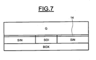
figure 7 montre le dispositif de lafigure 6 , après l'étape de remplissage de la cavité formée après l'étape de gravure.
- The
figure 1 is a sectional view of a semiconductor device in progress, showing the realization of the active by means of a method according to the state of the art; - The
figure 2 is another sectional view of a semiconductor device subsequent to a cleaning step prior to making the gate region by means of a method according to the state of the art; - The
figure 3 is a sectional view of a semiconductor device during a first phase of providing an isolation region by means of a method according to the invention; - The
figure 4 is a top view of a semiconductor device being implemented by means of a method according to the invention, after transformation of the silicon-germanium alloy isolation region and formation of the gate region; - The
figure 5 is a sectional view in another direction of the device of thefigure 4 , showing the realization of the spacers; - The
figure 6 is a sectional view of the device ofFigures 3 to 5 after the etching step; and - The
figure 7 shows the device of thefigure 6 after the step of filling the cavity formed after the etching step.
Sur les
Tel que représenté sur ces figures, le procédé consiste à réaliser des transistors MOS sur un substrat en silicium de type SOI (« Silicon On Insulator ») disposé sur une couche d'oxyde enterré BOX (« Buried OXide »).As shown in these figures, the method consists in producing MOS transistors on a Silicon On Insulator (SOI) type silicon substrate disposed on a BOX buried oxide layer ("Buried OXide").
Selon ce type de technologie, la couche d'oxyde enterré présente une épaisseur de l'ordre de 1500 Å.According to this type of technology, the buried oxide layer has a thickness of the order of 1500 Å.
L'étape de procédé représentée sur la
A ce stade, le substrat SOI est recouvert d'une couche de résine photo-sensible 10 avec interposition d'un masque dur 12 et d'une couche 13 de nitrure Si3N4.At this stage, the SOI substrate is covered with a photo-
En référence à la
Comme on le conçoit, selon cette technique, il n'est pas possible de réaliser des transistors sur un substrat déposé sur une couche d'oxyde enterré d'une épaisseur de l'ordre de 200 Å afin de limiter les couplages électriques et la création de lignes de champ entre le drain et la source du transistor à travers la couche de BOX et d'éviter l'intégration standard de la région d'isolation STI.As it is conceived, according to this technique, it is not possible to make transistors on a substrate deposited on a buried oxide layer of a thickness of the order of 200 Å in order to limit the electrical coupling and the creation of field lines between the drain and the transistor source across the BOX layer and to avoid the standard integration of the STI isolation region.
En outre, comme le révèle la
On va décrire, en référence aux
Le procédé décrit sur ces figures consiste à réaliser des transistors MOS sur un substrat semi-conducteur SOI disposé sur une couche d'oxyde enterré BOX.The method described in these figures consists in producing MOS transistors on an SOI semiconductor substrate disposed on a buried oxide layer BOX.
Comme cela sera décrit en détail par la suite, ce procédé permet la réalisation de transistors sur une couche d'oxyde d'épaisseur de l'ordre de 200 Å disposée au-dessus d'une couche d'oxyde enterré d'épaisseur également de l'ordre de 200 Å, voire 100 Å.As will be described in detail later, this method allows the realization of transistors on an oxide layer of thickness of the order of 200 Å disposed above a buried oxide layer of thickness also of the order of 200 Å or 100 Å.
En se référant tout d'abord à la
En se référant également à la
On enlève la résine puis on recuit le substrat pour obtenir une formation localisée d'un alliage de silicium-germanium, à l'endroit de la région d'isolation R.The resin is removed and the substrate is then annealed to obtain a localized formation of a silicon-germanium alloy at the location of the isolation region R.
En se référant également à la
Cette phase de formation de la grille est réalisée de manière conventionnelle et ne sera donc pas décrite en détail par la suite.This phase of forming the grid is performed in a conventional manner and will therefore not be described in detail later.
On notera cependant qu'elle consiste essentiellement à déposer une couche d'oxyde de grille 14 sur le substrat SOI, puis à déposer une couche de matériau de grille, par exemple du silicium polycristallin, sur la couche d'oxyde de grille. On procède alors à une étape de photolithographie suivie d'une étape de gravure, de manière à ne laisser subsister qu'un dépôt d'oxyde de grille recouvert de matériau de grille qu'à l'endroit de la région de grille pour le transistor à former.Note, however, that it consists essentially of depositing a
On procède alors à un dépôt, puis à une gravure de matériau pour espaceurs afin de réaliser les espaceurs E.This is followed by a deposition and then an etching of spacer material in order to make the spacers E.
Lors de l'étape suivante, c'est-à-dire après réalisation de la grille munie de ces espaceurs E, on procède à un retrait sélectif de l'alliage de silicium-germanium puis plus tard à une phase de siliciuration. Différentes techniques peuvent être utilisées pour le retrait sélectif de cet alliage de silicium-germanium. On peut ainsi, par exemple, utiliser une attaque plasma ou humide isotrope, une attaque chimique pouvant également être mise en oeuvre à cet effet.During the next step, that is to say after completion of the grid provided with these spacers E, selective removal of the silicon-germanium alloy is carried out, followed later by a silicidation phase. Various techniques can be used for the selective removal of this silicon-germanium alloy. We can thus, by For example, using an isotropic plasma or wet etching, a chemical etching can also be implemented for this purpose.
On notera que l'implantation ionique de germanium dans la région R du substrat destinée à constituer la région isolante, a été effectuée afin de former ultérieurement une zone localisée d'un alliage de silicium-germanium, lequel peut être sélectivement gravé par rapport au silicium du substrat SOI. Aussi, en variante, il est possible de réaliser une implantation localisée de tout autre matériau pouvant être sélectivement gravé par rapport au silicium. Toutefois, l'utilisation d'un alliage de silicium-germanium est avantageuse dans la mesure où la zone en alliage SiGe peut alors être réalisée aisément et relativement rapidement par des techniques conventionnelles.It will be noted that the ionic implantation of germanium in the region R of the substrate intended to constitute the insulating region has been carried out so as to subsequently form a localized zone of a silicon-germanium alloy, which may be selectively etched relative to silicon. SOI substrate. Also, alternatively, it is possible to perform localized implantation of any other material that can be selectively etched relative to silicon. However, the use of a silicon-germanium alloy is advantageous insofar as the SiGe alloy zone can then be easily and relatively quickly achieved by conventional techniques.
A l'issue de cette phase de gravure, le dispositif se situe dans l'étape visible à la
Lors de l'étape suivante, on procède à un dépôt de diélectrique pour remplir les cavités créées à l'issue de l'étape de gravure.In the next step, a dielectric deposit is made to fill the cavities created at the end of the etching step.
En référence à la
Comme on le voit sur cette figure, la face supérieure de la région R d'isolation affleure la face supérieure du silicium SOI.As seen in this figure, the upper face of the insulation region R is flush with the upper face of SOI silicon.
Enfin, de manière conventionnelle en SOI, il convient alors de former les régions de source et de drain par des techniques conventionnelles de photolithographie, d'implantation ionique et de siliciuration, puis de recouvrir l'ensemble par une couche de diélectrique PMD (Pré-Métal Diélectrique).Finally, conventionally in SOI, it is then necessary to form the source and drain regions by conventional techniques of photolithography, ion implantation and siliciding, and then to cover the assembly with a layer of PMD dielectric (Pre- Dielectric Metal).
Grâce au procédé qui vient d'être décrit, il a ainsi été possible de réaliser une région de grille sur un substrat SOI déposé sur une couche d'oxyde enterré BOX relativement mince, c'est-à-dire de l'ordre de 200 Å, dans la mesure où aucune étape de procédé ne conduit à une attaque de la couche d'oxyde BOX. En outre, la grille s'étend selon une surface parfaitement plane, évitant ainsi la création de transistors parasites latéraux.By means of the process just described, it has thus been possible to produce a gate region on an SOI substrate deposited on a relatively thin BOX buried oxide layer, that is to say on the order of 200 Å, since no process step leads to an attack of the oxide layer BOX. In addition, the grid extends in a perfectly flat surface, thus avoiding the creation of side parasitic transistors.
De surcroît, le procédé selon l'invention permet d'obtenir les avantages suivants :
- grâce à l'invention, il n'est pas nécessaire de prévoir une étape de formation d'un module STI pour réaliser la région d'isolation,
- la région d'isolation proprement dite peut être formée après la réalisation de la grille,
- le procédé, et en particulier le dépôt de diélectrique, peut s'effectuer à basse température, adaptable à différentes technologies,
- le procédé permet de contraindre le canal du transistor par dépôt, par exemple, de nitrure de silicium SiN tensile ou compressif au niveau de la région d'isolation.
- L'intérêt d'avoir du SiGe permet, entre autre, d'avoir un matériau monocristallin pour la croissance de l'oxyde de grille et de limiter les problèmes de fiabilité d'oxyde par rapport à un matériau par exemple de type Si3N4.
- thanks to the invention, it is not necessary to provide a step of forming an STI module to produce the isolation region,
- the insulation region itself can be formed after the realization of the grid,
- the process, and in particular the deposition of dielectric, can be carried out at low temperature, adaptable to different technologies,
- the method makes it possible to constrain the transistor channel by deposition, for example, of tensile or compressive SiN silicon nitride at the level of the isolation region.
- The advantage of having SiGe makes it possible, among other things, to have a monocrystalline material for the growth of the oxide of grid and to limit the problems of reliability of oxide with respect to a material for example of type Si 3 N 4 .
Claims (7)
- Process for producing an MOS transistor on a silicon substrate (SOI) placed on a buried oxide layer (BOX), said transistor being produced in an active substrate zone defined by an isolating region (R), the process comprising the steps of:1. definition of the isolating region, which is produced by localized formation of a zone of material that can be selectively etched with respect to silicon; and then2. production of a gate region (G) and source and drain regions, which between them define a channel so that the gate region extends above the channel; and then3. selective etching of said material that can be selectively etched with respect to silicon and deposition of a dielectric material in the etched feature.
- Process according to Claim 1, characterized in that a germanium ion implantation is carried out in the isolating region (R), the substrate (SOI) is annealed so as locally to convert silicon into a silicon-germanium alloy, a layer of gate material is deposited on the substrate, with interposition of a gate oxide layer (14), an etching step is carried out in the silicon-germanium alloy zone, so as to remove said alloy, and said dielectric material is deposited in said etched zone.
- Process according to Claim 2, characterized in that spacers (E) for the gate are formed before the silicon-germanium is etched.
- Process according to Claim 3, characterized in that the dielectric deposited is a dielectric of the same type as that of the spacers.
- Process according to any one of Claims 2 to 4, characterized in that the etching step is either an isotropic plasma etching step or an isotropic wet etching step.
- Process according to any one of Claims 2 to 5, characterized in that the etching step is carried out so as to etch the silicon-germanium alloy down to the underlying oxide layer.
- Process according to one of Claims 4 to 6, characterized in that the dielectric is silicon nitride.
Applications Claiming Priority (1)
| Application Number | Priority Date | Filing Date | Title |
|---|---|---|---|
| FR0507598A FR2888665B1 (en) | 2005-07-18 | 2005-07-18 | METHOD FOR PRODUCING A MOS TRANSISTOR AND CORRESPONDING INTEGRATED CIRCUIT |
Publications (2)
| Publication Number | Publication Date |
|---|---|
| EP1746643A1 EP1746643A1 (en) | 2007-01-24 |
| EP1746643B1 true EP1746643B1 (en) | 2015-09-02 |
Family
ID=36228787
Family Applications (1)
| Application Number | Title | Priority Date | Filing Date |
|---|---|---|---|
| EP06291159.9A Active EP1746643B1 (en) | 2005-07-18 | 2006-07-18 | Process of making a MOS transistor. |
Country Status (3)
| Country | Link |
|---|---|
| US (2) | US7749858B2 (en) |
| EP (1) | EP1746643B1 (en) |
| FR (1) | FR2888665B1 (en) |
Families Citing this family (1)
| Publication number | Priority date | Publication date | Assignee | Title |
|---|---|---|---|---|
| CN111785616B (en) * | 2019-04-04 | 2023-06-23 | 上海新微技术研发中心有限公司 | Preparation method of selected-area germanium-lead alloy based on ion implantation and annealing method |
Citations (3)
| Publication number | Priority date | Publication date | Assignee | Title |
|---|---|---|---|---|
| EP1365447A2 (en) * | 2002-05-23 | 2003-11-26 | Sharp Kabushiki Kaisha | Manufacturing method of semiconductor substrate |
| US20040195623A1 (en) * | 2003-04-03 | 2004-10-07 | Chung-Hu Ge | Strained channel on insulator device |
| US20050151222A1 (en) * | 2004-01-12 | 2005-07-14 | Advanced Micro Devices, Inc. | Shallow trench isolation process and structure with minimized strained silicon consumption |
Family Cites Families (11)
| Publication number | Priority date | Publication date | Assignee | Title |
|---|---|---|---|---|
| US5436174A (en) * | 1993-01-25 | 1995-07-25 | North Carolina State University | Method of forming trenches in monocrystalline silicon carbide |
| WO1997039476A1 (en) * | 1996-04-18 | 1997-10-23 | Matsushita Electric Industrial Co., Ltd. | SiC ELEMENT AND PROCESS FOR ITS PRODUCTION |
| US5949126A (en) * | 1997-12-17 | 1999-09-07 | Advanced Micro Devices, Inc. | Trench isolation structure employing protective sidewall spacers upon exposed surfaces of the isolation trench |
| US6633066B1 (en) * | 2000-01-07 | 2003-10-14 | Samsung Electronics Co., Ltd. | CMOS integrated circuit devices and substrates having unstrained silicon active layers |
| ITMI20010339A1 (en) * | 2001-02-20 | 2002-08-20 | St Microelectronics Srl | METHOD TO CREATE INSULATING STRUCTURES |
| US6969618B2 (en) * | 2002-08-23 | 2005-11-29 | Micron Technology, Inc. | SOI device having increased reliability and reduced free floating body effects |
| US20040242015A1 (en) * | 2003-03-04 | 2004-12-02 | Kyoung-Chul Kim | Etching compositions for silicon germanium and etching methods using the same |
| US6924182B1 (en) * | 2003-08-15 | 2005-08-02 | Advanced Micro Devices, Inc. | Strained silicon MOSFET having reduced leakage and method of its formation |
| US7119404B2 (en) * | 2004-05-19 | 2006-10-10 | Taiwan Semiconductor Manufacturing Co. Ltd. | High performance strained channel MOSFETs by coupled stress effects |
| JP4811901B2 (en) * | 2004-06-03 | 2011-11-09 | ルネサスエレクトロニクス株式会社 | Semiconductor device |
| KR100606925B1 (en) * | 2004-12-30 | 2006-08-01 | 동부일렉트로닉스 주식회사 | A method for fabricating a fin-FET |
-
2005
- 2005-07-18 FR FR0507598A patent/FR2888665B1/en not_active Expired - Fee Related
-
2006
- 2006-07-17 US US11/487,706 patent/US7749858B2/en active Active
- 2006-07-18 EP EP06291159.9A patent/EP1746643B1/en active Active
-
2010
- 2010-05-25 US US12/787,193 patent/US20100230755A1/en not_active Abandoned
Patent Citations (3)
| Publication number | Priority date | Publication date | Assignee | Title |
|---|---|---|---|---|
| EP1365447A2 (en) * | 2002-05-23 | 2003-11-26 | Sharp Kabushiki Kaisha | Manufacturing method of semiconductor substrate |
| US20040195623A1 (en) * | 2003-04-03 | 2004-10-07 | Chung-Hu Ge | Strained channel on insulator device |
| US20050151222A1 (en) * | 2004-01-12 | 2005-07-14 | Advanced Micro Devices, Inc. | Shallow trench isolation process and structure with minimized strained silicon consumption |
Also Published As
| Publication number | Publication date |
|---|---|
| US20100230755A1 (en) | 2010-09-16 |
| US20070037324A1 (en) | 2007-02-15 |
| FR2888665A1 (en) | 2007-01-19 |
| FR2888665B1 (en) | 2007-10-19 |
| US7749858B2 (en) | 2010-07-06 |
| EP1746643A1 (en) | 2007-01-24 |
Similar Documents
| Publication | Publication Date | Title |
|---|---|---|
| EP1837916B1 (en) | Method of manufacturing a transistor having a channel comprising germanium | |
| EP1091417A1 (en) | Method for fabricating a semiconductor device with a gate-all-around and device formed thereby | |
| FR2838238A1 (en) | Semiconductor device with enveloping gate encapsulated in an insulating medium | |
| EP1589572B1 (en) | Process of making an integrated circuit comprising hollow trench isolation | |
| FR2823009A1 (en) | Vertical transistor production with insulated gate with weak overlapping of gate on source and drain comprises forming vertical semiconductor column by anisotropic engraving and formation of insulated dielectric gate | |
| FR3043837A1 (en) | METHOD FOR PRODUCING A SEMICONDUCTOR NANOFIL TRANSISTOR COMPRISING A SELF-ALIGNED GRID AND SPACERS | |
| FR2823010A1 (en) | Insulated-gate vertical transistor production comprises forming semiconductor column on semiconductor substrate, and forming insulated semiconductor gate on column sides and substrate upper surface | |
| EP2779223B1 (en) | Method for producing a substrate provided with edge protection | |
| EP1788635B1 (en) | Method of manufacturing a self-aligned dual-gates transistor through gate pattern reduction | |
| EP2610915A1 (en) | Transistor and method for manufacturing a transistor | |
| EP2999001A2 (en) | Production of spacers at the edges of a transistor gate | |
| FR2990295A1 (en) | METHOD OF FORMING GRID, SOURCE AND DRAIN CONTACTS ON MOS TRANSISTOR | |
| FR3011119A1 (en) | METHOD FOR PRODUCING A TRANSISTOR | |
| EP3503175A1 (en) | Method for producing a semiconductor substrate comprising at least one portion of semiconductor subjected to compressive strain | |
| EP3246948B1 (en) | Method for forming, on a single substrate, transistors having different characteristics | |
| EP2120258A1 (en) | Method for manufacturing a transistor with metal source and drain | |
| FR3034254A1 (en) | METHOD OF MAKING A SOI-TYPE SUBSTRATE, ESPECIALLY FDSOI, ADAPTED TO TRANSISTORS HAVING DIELECTRICS OF DIFFERENT THICKNESS GRIDS, SUBSTRATE AND INTEGRATED CIRCUIT CORRESPONDING | |
| EP1746643B1 (en) | Process of making a MOS transistor. | |
| EP1407486B1 (en) | Method for making a transistor on a soi substrate | |
| EP1615271A1 (en) | Method of straining a thin film pattern | |
| FR2976401A1 (en) | ELECTRONIC COMPONENT COMPRISING A MOSFET TRANSISTOR ASSEMBLY AND METHOD FOR MANUFACTURING | |
| FR2860919A1 (en) | Semiconductor on Insulator regions destined to receive components with an over thickness, notably for the fabrication of MOS transistor | |
| FR3037714A1 (en) | METHOD FOR MAKING A CONTACT ON AN ACTIVE ZONE OF AN INTEGRATED CIRCUIT, FOR EXAMPLE ON A SOI SUBSTRATE, IN PARTICULAR FDSOI, AND INTEGRATED CIRCUIT CORRESPONDING | |
| WO2006070154A1 (en) | Improved semiconductor thin-film transistor structure | |
| EP2428985B1 (en) | Method for manufacturing a strained channel MOS transistor |
Legal Events
| Date | Code | Title | Description |
|---|---|---|---|
| PUAI | Public reference made under article 153(3) epc to a published international application that has entered the european phase |
Free format text: ORIGINAL CODE: 0009012 |
|
| AK | Designated contracting states |
Kind code of ref document: A1 Designated state(s): AT BE BG CH CY CZ DE DK EE ES FI FR GB GR HU IE IS IT LI LT LU LV MC NL PL PT RO SE SI SK TR |
|
| AX | Request for extension of the european patent |
Extension state: AL BA HR MK YU |
|
| 17P | Request for examination filed |
Effective date: 20070627 |
|
| 17Q | First examination report despatched |
Effective date: 20070806 |
|
| AKX | Designation fees paid |
Designated state(s): DE FR GB IT |
|
| RAP1 | Party data changed (applicant data changed or rights of an application transferred) |
Owner name: STMICROELECTRONICS (CROLLES 2) SAS Owner name: COMMISSARIAT A L'ENERGIE ATOMIQUE ET AUX ENERGIES |
|
| GRAP | Despatch of communication of intention to grant a patent |
Free format text: ORIGINAL CODE: EPIDOSNIGR1 |
|
| INTG | Intention to grant announced |
Effective date: 20150318 |
|
| GRAS | Grant fee paid |
Free format text: ORIGINAL CODE: EPIDOSNIGR3 |
|
| GRAA | (expected) grant |
Free format text: ORIGINAL CODE: 0009210 |
|
| AK | Designated contracting states |
Kind code of ref document: B1 Designated state(s): DE FR GB IT |
|
| REG | Reference to a national code |
Ref country code: GB Ref legal event code: FG4D Free format text: NOT ENGLISH |
|
| REG | Reference to a national code |
Ref country code: DE Ref legal event code: R096 Ref document number: 602006046491 Country of ref document: DE |
|
| PG25 | Lapsed in a contracting state [announced via postgrant information from national office to epo] |
Ref country code: IT Free format text: LAPSE BECAUSE OF FAILURE TO SUBMIT A TRANSLATION OF THE DESCRIPTION OR TO PAY THE FEE WITHIN THE PRESCRIBED TIME-LIMIT Effective date: 20150902 |
|
| REG | Reference to a national code |
Ref country code: DE Ref legal event code: R097 Ref document number: 602006046491 Country of ref document: DE |
|
| REG | Reference to a national code |
Ref country code: FR Ref legal event code: PLFP Year of fee payment: 11 |
|
| PLBE | No opposition filed within time limit |
Free format text: ORIGINAL CODE: 0009261 |
|
| STAA | Information on the status of an ep patent application or granted ep patent |
Free format text: STATUS: NO OPPOSITION FILED WITHIN TIME LIMIT |
|
| 26N | No opposition filed |
Effective date: 20160603 |
|
| REG | Reference to a national code |
Ref country code: DE Ref legal event code: R119 Ref document number: 602006046491 Country of ref document: DE |
|
| GBPC | Gb: european patent ceased through non-payment of renewal fee |
Effective date: 20160718 |
|
| PG25 | Lapsed in a contracting state [announced via postgrant information from national office to epo] |
Ref country code: DE Free format text: LAPSE BECAUSE OF NON-PAYMENT OF DUE FEES Effective date: 20170201 |
|
| PG25 | Lapsed in a contracting state [announced via postgrant information from national office to epo] |
Ref country code: GB Free format text: LAPSE BECAUSE OF NON-PAYMENT OF DUE FEES Effective date: 20160718 |
|
| REG | Reference to a national code |
Ref country code: FR Ref legal event code: PLFP Year of fee payment: 12 |
|
| REG | Reference to a national code |
Ref country code: FR Ref legal event code: PLFP Year of fee payment: 13 |
|
| PGFP | Annual fee paid to national office [announced via postgrant information from national office to epo] |
Ref country code: FR Payment date: 20230615 Year of fee payment: 18 |