EP1734302A1 - A light emitting device - Google Patents
A light emitting device Download PDFInfo
- Publication number
- EP1734302A1 EP1734302A1 EP06253028A EP06253028A EP1734302A1 EP 1734302 A1 EP1734302 A1 EP 1734302A1 EP 06253028 A EP06253028 A EP 06253028A EP 06253028 A EP06253028 A EP 06253028A EP 1734302 A1 EP1734302 A1 EP 1734302A1
- Authority
- EP
- European Patent Office
- Prior art keywords
- light emitting
- light
- wavelength conversion
- emitting device
- heat conduction
- Prior art date
- Legal status (The legal status is an assumption and is not a legal conclusion. Google has not performed a legal analysis and makes no representation as to the accuracy of the status listed.)
- Granted
Links
- 238000006243 chemical reaction Methods 0.000 claims abstract description 85
- 239000000463 material Substances 0.000 claims description 32
- 238000007747 plating Methods 0.000 claims description 11
- 239000013307 optical fiber Substances 0.000 claims description 7
- 230000015556 catabolic process Effects 0.000 description 15
- 238000006731 degradation reaction Methods 0.000 description 15
- 238000000034 method Methods 0.000 description 10
- 238000010586 diagram Methods 0.000 description 7
- 229910002601 GaN Inorganic materials 0.000 description 6
- JMASRVWKEDWRBT-UHFFFAOYSA-N Gallium nitride Chemical compound [Ga]#N JMASRVWKEDWRBT-UHFFFAOYSA-N 0.000 description 6
- MCMNRKCIXSYSNV-UHFFFAOYSA-N Zirconium dioxide Chemical compound O=[Zr]=O MCMNRKCIXSYSNV-UHFFFAOYSA-N 0.000 description 6
- 230000002349 favourable effect Effects 0.000 description 6
- 229910052751 metal Inorganic materials 0.000 description 6
- 239000002184 metal Substances 0.000 description 6
- PXHVJJICTQNCMI-UHFFFAOYSA-N Nickel Chemical compound [Ni] PXHVJJICTQNCMI-UHFFFAOYSA-N 0.000 description 5
- PNEYBMLMFCGWSK-UHFFFAOYSA-N aluminium oxide Inorganic materials [O-2].[O-2].[O-2].[Al+3].[Al+3] PNEYBMLMFCGWSK-UHFFFAOYSA-N 0.000 description 5
- 238000002845 discoloration Methods 0.000 description 5
- 239000011521 glass Substances 0.000 description 5
- 238000002310 reflectometry Methods 0.000 description 5
- VYPSYNLAJGMNEJ-UHFFFAOYSA-N Silicium dioxide Chemical compound O=[Si]=O VYPSYNLAJGMNEJ-UHFFFAOYSA-N 0.000 description 4
- 230000004907 flux Effects 0.000 description 4
- 230000017525 heat dissipation Effects 0.000 description 4
- 239000000203 mixture Substances 0.000 description 4
- 230000003287 optical effect Effects 0.000 description 4
- 238000004544 sputter deposition Methods 0.000 description 4
- 239000000126 substance Substances 0.000 description 4
- KFZMGEQAYNKOFK-UHFFFAOYSA-N Isopropanol Chemical compound CC(C)O KFZMGEQAYNKOFK-UHFFFAOYSA-N 0.000 description 3
- BQCADISMDOOEFD-UHFFFAOYSA-N Silver Chemical compound [Ag] BQCADISMDOOEFD-UHFFFAOYSA-N 0.000 description 3
- 238000005253 cladding Methods 0.000 description 3
- 239000010949 copper Substances 0.000 description 3
- 239000000945 filler Substances 0.000 description 3
- 238000002156 mixing Methods 0.000 description 3
- 239000011368 organic material Substances 0.000 description 3
- 239000004065 semiconductor Substances 0.000 description 3
- 229920002050 silicone resin Polymers 0.000 description 3
- 229910052709 silver Inorganic materials 0.000 description 3
- 239000004332 silver Substances 0.000 description 3
- XOLBLPGZBRYERU-UHFFFAOYSA-N tin dioxide Chemical compound O=[Sn]=O XOLBLPGZBRYERU-UHFFFAOYSA-N 0.000 description 3
- CSCPPACGZOOCGX-UHFFFAOYSA-N Acetone Chemical compound CC(C)=O CSCPPACGZOOCGX-UHFFFAOYSA-N 0.000 description 2
- PIGFYZPCRLYGLF-UHFFFAOYSA-N Aluminum nitride Chemical compound [Al]#N PIGFYZPCRLYGLF-UHFFFAOYSA-N 0.000 description 2
- LFQSCWFLJHTTHZ-UHFFFAOYSA-N Ethanol Chemical compound CCO LFQSCWFLJHTTHZ-UHFFFAOYSA-N 0.000 description 2
- 230000002411 adverse Effects 0.000 description 2
- 239000003513 alkali Substances 0.000 description 2
- 230000000052 comparative effect Effects 0.000 description 2
- PMHQVHHXPFUNSP-UHFFFAOYSA-M copper(1+);methylsulfanylmethane;bromide Chemical compound Br[Cu].CSC PMHQVHHXPFUNSP-UHFFFAOYSA-M 0.000 description 2
- 239000010432 diamond Substances 0.000 description 2
- 229910003460 diamond Inorganic materials 0.000 description 2
- 230000000694 effects Effects 0.000 description 2
- 238000004070 electrodeposition Methods 0.000 description 2
- 229910003437 indium oxide Inorganic materials 0.000 description 2
- PJXISJQVUVHSOJ-UHFFFAOYSA-N indium(iii) oxide Chemical compound [O-2].[O-2].[O-2].[In+3].[In+3] PJXISJQVUVHSOJ-UHFFFAOYSA-N 0.000 description 2
- 239000000395 magnesium oxide Substances 0.000 description 2
- CPLXHLVBOLITMK-UHFFFAOYSA-N magnesium oxide Inorganic materials [Mg]=O CPLXHLVBOLITMK-UHFFFAOYSA-N 0.000 description 2
- AXZKOIWUVFPNLO-UHFFFAOYSA-N magnesium;oxygen(2-) Chemical compound [O-2].[Mg+2] AXZKOIWUVFPNLO-UHFFFAOYSA-N 0.000 description 2
- 230000004048 modification Effects 0.000 description 2
- 238000012986 modification Methods 0.000 description 2
- 229910052759 nickel Inorganic materials 0.000 description 2
- 238000004382 potting Methods 0.000 description 2
- 239000010453 quartz Substances 0.000 description 2
- 238000009877 rendering Methods 0.000 description 2
- HBMJWWWQQXIZIP-UHFFFAOYSA-N silicon carbide Chemical compound [Si+]#[C-] HBMJWWWQQXIZIP-UHFFFAOYSA-N 0.000 description 2
- XLYOFNOQVPJJNP-UHFFFAOYSA-N water Substances O XLYOFNOQVPJJNP-UHFFFAOYSA-N 0.000 description 2
- OKTJSMMVPCPJKN-UHFFFAOYSA-N Carbon Chemical compound [C] OKTJSMMVPCPJKN-UHFFFAOYSA-N 0.000 description 1
- RYGMFSIKBFXOCR-UHFFFAOYSA-N Copper Chemical compound [Cu] RYGMFSIKBFXOCR-UHFFFAOYSA-N 0.000 description 1
- 239000001856 Ethyl cellulose Substances 0.000 description 1
- ZZSNKZQZMQGXPY-UHFFFAOYSA-N Ethyl cellulose Chemical compound CCOCC1OC(OC)C(OCC)C(OCC)C1OC1C(O)C(O)C(OC)C(CO)O1 ZZSNKZQZMQGXPY-UHFFFAOYSA-N 0.000 description 1
- 229910052688 Gadolinium Inorganic materials 0.000 description 1
- VEXZGXHMUGYJMC-UHFFFAOYSA-N Hydrochloric acid Chemical compound Cl VEXZGXHMUGYJMC-UHFFFAOYSA-N 0.000 description 1
- 229910000831 Steel Inorganic materials 0.000 description 1
- XLOMVQKBTHCTTD-UHFFFAOYSA-N Zinc monoxide Chemical compound [Zn]=O XLOMVQKBTHCTTD-UHFFFAOYSA-N 0.000 description 1
- WUOACPNHFRMFPN-UHFFFAOYSA-N alpha-terpineol Chemical compound CC1=CCC(C(C)(C)O)CC1 WUOACPNHFRMFPN-UHFFFAOYSA-N 0.000 description 1
- 229910052782 aluminium Inorganic materials 0.000 description 1
- XAGFODPZIPBFFR-UHFFFAOYSA-N aluminium Chemical compound [Al] XAGFODPZIPBFFR-UHFFFAOYSA-N 0.000 description 1
- 238000004380 ashing Methods 0.000 description 1
- TZCXTZWJZNENPQ-UHFFFAOYSA-L barium sulfate Chemical compound [Ba+2].[O-]S([O-])(=O)=O TZCXTZWJZNENPQ-UHFFFAOYSA-L 0.000 description 1
- 239000005388 borosilicate glass Substances 0.000 description 1
- 229910052799 carbon Inorganic materials 0.000 description 1
- 238000004140 cleaning Methods 0.000 description 1
- 239000011248 coating agent Substances 0.000 description 1
- 238000000576 coating method Methods 0.000 description 1
- 229910052681 coesite Inorganic materials 0.000 description 1
- 239000003086 colorant Substances 0.000 description 1
- 239000000470 constituent Substances 0.000 description 1
- 229910052802 copper Inorganic materials 0.000 description 1
- 229910052593 corundum Inorganic materials 0.000 description 1
- 229910052906 cristobalite Inorganic materials 0.000 description 1
- 238000005238 degreasing Methods 0.000 description 1
- SQIFACVGCPWBQZ-UHFFFAOYSA-N delta-terpineol Natural products CC(C)(O)C1CCC(=C)CC1 SQIFACVGCPWBQZ-UHFFFAOYSA-N 0.000 description 1
- 238000001035 drying Methods 0.000 description 1
- 238000000295 emission spectrum Methods 0.000 description 1
- 239000003822 epoxy resin Substances 0.000 description 1
- 229920001249 ethyl cellulose Polymers 0.000 description 1
- 235000019325 ethyl cellulose Nutrition 0.000 description 1
- 239000000835 fiber Substances 0.000 description 1
- 238000010438 heat treatment Methods 0.000 description 1
- 238000005286 illumination Methods 0.000 description 1
- 238000003384 imaging method Methods 0.000 description 1
- AMGQUBHHOARCQH-UHFFFAOYSA-N indium;oxotin Chemical compound [In].[Sn]=O AMGQUBHHOARCQH-UHFFFAOYSA-N 0.000 description 1
- 229910010272 inorganic material Inorganic materials 0.000 description 1
- 239000011147 inorganic material Substances 0.000 description 1
- 239000007788 liquid Substances 0.000 description 1
- 238000004519 manufacturing process Methods 0.000 description 1
- 238000002844 melting Methods 0.000 description 1
- 230000002093 peripheral effect Effects 0.000 description 1
- 229920002120 photoresistant polymer Polymers 0.000 description 1
- 229920000647 polyepoxide Polymers 0.000 description 1
- 229920005989 resin Polymers 0.000 description 1
- 239000011347 resin Substances 0.000 description 1
- 239000000377 silicon dioxide Substances 0.000 description 1
- 238000005245 sintering Methods 0.000 description 1
- 238000001228 spectrum Methods 0.000 description 1
- 229910001220 stainless steel Inorganic materials 0.000 description 1
- 239000010935 stainless steel Substances 0.000 description 1
- 239000010959 steel Substances 0.000 description 1
- 229910052682 stishovite Inorganic materials 0.000 description 1
- 229940116411 terpineol Drugs 0.000 description 1
- 229910001887 tin oxide Inorganic materials 0.000 description 1
- 229910052905 tridymite Inorganic materials 0.000 description 1
- 238000007740 vapor deposition Methods 0.000 description 1
- 229910001845 yogo sapphire Inorganic materials 0.000 description 1
Images


Classifications
-
- A—HUMAN NECESSITIES
- A61—MEDICAL OR VETERINARY SCIENCE; HYGIENE
- A61B—DIAGNOSIS; SURGERY; IDENTIFICATION
- A61B1/00—Instruments for performing medical examinations of the interior of cavities or tubes of the body by visual or photographical inspection, e.g. endoscopes; Illuminating arrangements therefor
- A61B1/06—Instruments for performing medical examinations of the interior of cavities or tubes of the body by visual or photographical inspection, e.g. endoscopes; Illuminating arrangements therefor with illuminating arrangements
- A61B1/0653—Instruments for performing medical examinations of the interior of cavities or tubes of the body by visual or photographical inspection, e.g. endoscopes; Illuminating arrangements therefor with illuminating arrangements with wavelength conversion
-
- A—HUMAN NECESSITIES
- A61—MEDICAL OR VETERINARY SCIENCE; HYGIENE
- A61B—DIAGNOSIS; SURGERY; IDENTIFICATION
- A61B1/00—Instruments for performing medical examinations of the interior of cavities or tubes of the body by visual or photographical inspection, e.g. endoscopes; Illuminating arrangements therefor
- A61B1/12—Instruments for performing medical examinations of the interior of cavities or tubes of the body by visual or photographical inspection, e.g. endoscopes; Illuminating arrangements therefor with cooling or rinsing arrangements
- A61B1/128—Instruments for performing medical examinations of the interior of cavities or tubes of the body by visual or photographical inspection, e.g. endoscopes; Illuminating arrangements therefor with cooling or rinsing arrangements provided with means for regulating temperature
-
- A—HUMAN NECESSITIES
- A61—MEDICAL OR VETERINARY SCIENCE; HYGIENE
- A61B—DIAGNOSIS; SURGERY; IDENTIFICATION
- A61B90/00—Instruments, implements or accessories specially adapted for surgery or diagnosis and not covered by any of the groups A61B1/00 - A61B50/00, e.g. for luxation treatment or for protecting wound edges
- A61B90/36—Image-producing devices or illumination devices not otherwise provided for
-
- F—MECHANICAL ENGINEERING; LIGHTING; HEATING; WEAPONS; BLASTING
- F21—LIGHTING
- F21S—NON-PORTABLE LIGHTING DEVICES; SYSTEMS THEREOF; VEHICLE LIGHTING DEVICES SPECIALLY ADAPTED FOR VEHICLE EXTERIORS
- F21S41/00—Illuminating devices specially adapted for vehicle exteriors, e.g. headlamps
- F21S41/10—Illuminating devices specially adapted for vehicle exteriors, e.g. headlamps characterised by the light source
- F21S41/14—Illuminating devices specially adapted for vehicle exteriors, e.g. headlamps characterised by the light source characterised by the type of light source
- F21S41/16—Laser light sources
-
- F—MECHANICAL ENGINEERING; LIGHTING; HEATING; WEAPONS; BLASTING
- F21—LIGHTING
- F21S—NON-PORTABLE LIGHTING DEVICES; SYSTEMS THEREOF; VEHICLE LIGHTING DEVICES SPECIALLY ADAPTED FOR VEHICLE EXTERIORS
- F21S41/00—Illuminating devices specially adapted for vehicle exteriors, e.g. headlamps
- F21S41/10—Illuminating devices specially adapted for vehicle exteriors, e.g. headlamps characterised by the light source
- F21S41/14—Illuminating devices specially adapted for vehicle exteriors, e.g. headlamps characterised by the light source characterised by the type of light source
- F21S41/176—Light sources where the light is generated by photoluminescent material spaced from a primary light generating element
-
- F—MECHANICAL ENGINEERING; LIGHTING; HEATING; WEAPONS; BLASTING
- F21—LIGHTING
- F21S—NON-PORTABLE LIGHTING DEVICES; SYSTEMS THEREOF; VEHICLE LIGHTING DEVICES SPECIALLY ADAPTED FOR VEHICLE EXTERIORS
- F21S41/00—Illuminating devices specially adapted for vehicle exteriors, e.g. headlamps
- F21S41/10—Illuminating devices specially adapted for vehicle exteriors, e.g. headlamps characterised by the light source
- F21S41/19—Attachment of light sources or lamp holders
-
- G—PHYSICS
- G02—OPTICS
- G02B—OPTICAL ELEMENTS, SYSTEMS OR APPARATUS
- G02B6/00—Light guides; Structural details of arrangements comprising light guides and other optical elements, e.g. couplings
- G02B6/24—Coupling light guides
- G02B6/42—Coupling light guides with opto-electronic elements
- G02B6/4201—Packages, e.g. shape, construction, internal or external details
- G02B6/4202—Packages, e.g. shape, construction, internal or external details for coupling an active element with fibres without intermediate optical elements, e.g. fibres with plane ends, fibres with shaped ends, bundles
-
- A—HUMAN NECESSITIES
- A61—MEDICAL OR VETERINARY SCIENCE; HYGIENE
- A61B—DIAGNOSIS; SURGERY; IDENTIFICATION
- A61B18/00—Surgical instruments, devices or methods for transferring non-mechanical forms of energy to or from the body
- A61B18/18—Surgical instruments, devices or methods for transferring non-mechanical forms of energy to or from the body by applying electromagnetic radiation, e.g. microwaves
- A61B18/20—Surgical instruments, devices or methods for transferring non-mechanical forms of energy to or from the body by applying electromagnetic radiation, e.g. microwaves using laser
- A61B18/22—Surgical instruments, devices or methods for transferring non-mechanical forms of energy to or from the body by applying electromagnetic radiation, e.g. microwaves using laser the beam being directed along or through a flexible conduit, e.g. an optical fibre; Couplings or hand-pieces therefor
- A61B2018/2255—Optical elements at the distal end of probe tips
- A61B2018/2288—Optical elements at the distal end of probe tips the optical fibre cable having a curved distal end
-
- A—HUMAN NECESSITIES
- A61—MEDICAL OR VETERINARY SCIENCE; HYGIENE
- A61B—DIAGNOSIS; SURGERY; IDENTIFICATION
- A61B90/00—Instruments, implements or accessories specially adapted for surgery or diagnosis and not covered by any of the groups A61B1/00 - A61B50/00, e.g. for luxation treatment or for protecting wound edges
- A61B90/30—Devices for illuminating a surgical field, the devices having an interrelation with other surgical devices or with a surgical procedure
- A61B2090/306—Devices for illuminating a surgical field, the devices having an interrelation with other surgical devices or with a surgical procedure using optical fibres
-
- H—ELECTRICITY
- H01—ELECTRIC ELEMENTS
- H01S—DEVICES USING THE PROCESS OF LIGHT AMPLIFICATION BY STIMULATED EMISSION OF RADIATION [LASER] TO AMPLIFY OR GENERATE LIGHT; DEVICES USING STIMULATED EMISSION OF ELECTROMAGNETIC RADIATION IN WAVE RANGES OTHER THAN OPTICAL
- H01S5/00—Semiconductor lasers
- H01S5/005—Optical components external to the laser cavity, specially adapted therefor, e.g. for homogenisation or merging of the beams or for manipulating laser pulses, e.g. pulse shaping
- H01S5/0087—Optical components external to the laser cavity, specially adapted therefor, e.g. for homogenisation or merging of the beams or for manipulating laser pulses, e.g. pulse shaping for illuminating phosphorescent or fluorescent materials, e.g. using optical arrangements specifically adapted for guiding or shaping laser beams illuminating these materials
-
- H—ELECTRICITY
- H01—ELECTRIC ELEMENTS
- H01S—DEVICES USING THE PROCESS OF LIGHT AMPLIFICATION BY STIMULATED EMISSION OF RADIATION [LASER] TO AMPLIFY OR GENERATE LIGHT; DEVICES USING STIMULATED EMISSION OF ELECTROMAGNETIC RADIATION IN WAVE RANGES OTHER THAN OPTICAL
- H01S5/00—Semiconductor lasers
- H01S5/02—Structural details or components not essential to laser action
- H01S5/022—Mountings; Housings
- H01S5/0225—Out-coupling of light
- H01S5/02251—Out-coupling of light using optical fibres
Definitions
- the present invention relates to a light emitting device having a light emitting element, a light guide member, and a wavelength conversion member.
- LEDs light emitting diodes
- LDs laser diodes
- other such light emitting elements as the light source for such devices has already been proposed (see, for example, WO01/040702 ).
- LEDs and LDs are compact, have good power efficiency, emit light in vivid colors, and eliminate problems such as broken bulbs.
- LDs have higher optical density than LEDs, so a light emitting device of higher brightness can be obtained.
- the wavelength conversion member when light is emitted from an LED or LD to the outside via a wavelength conversion member, the wavelength conversion member is degraded by heat originating in the light, so that light from the light emitting element can no longer be fully emitted to the outside, or in some cases, the wavelength conversion member becomes discolored and makes the light emitting device unusable, among other such problems.
- a light emitting device comprising at least: a light emitting element; a wavelength conversion member for converting the wavelength of light from the light emitting element; a bendable light guide member for guiding light from the light emitting element to the wavelength conversion member; and a heat conduction member that is thermally connected to the wavelength conversion member.
- a light emitting device embodying the present invention will now be described through reference to the drawings.
- the light emitting devices discussed below are merely given to embody the technological concept of the present invention, and the present invention is not limited thereto.
- the dimensions, materials, shapes, relative layouts, and so forth of the constituent members are nothing more than illustrative examples, and should not be construed to limit the scope of the present invention to just these.
- the sizes, positional relationships, and so forth of the members shown in the drawings may be exaggerated in order to clarify the description.
- the elements that make up an embodiment of the present invention may be such that a plurality of elements are constituted by a single member, or conversely, a single element may be constituted by a plurality of members.
- FIG. 1 is a simplified overall diagram of a light emitting device embodying the present invention
- FIG. 2 is a simplified diagram of the detailed structured near the distal end of the light emitting device embodying the present invention.
- the light emitting device embodying the present invention is made up primarily of a light emitting element 10, a light guide member 20, a wavelength conversion member 40, and a heat conduction member 50 that is thermally connected to the wavelength conversion member 40. This allows heat generated in the wavelength conversion member 40 by light from the light emitting element 10 to be effectively taken away by the heat conduction member 50, and mitigates the degradation and discoloration caused by heat to the wavelength conversion member 40 and its peripheral members.
- thermally connected does not necessarily mean that one member is directly and completely connected physically to another member.
- one member may be indirectly connected with another member via yet another member, or one member may be partially in contact with another member.
- the light emitting element 10 there are no particular restrictions on the light emitting element 10, but an LD or LED can be used favorably. Using one of these affords a light emitting device with excellent initial drive characteristics, good durability in terms of vibration and repeated on/off flashing, a compact size, and high light emission output.
- an LD has higher optical density than an LED
- the use of an LD allows the brightness of the light emitting device to be easily increased, but this same high optical density also means that the wavelength conversion member 40 will be more apt to generate heat that can lead to degradation and discoloration.
- An embodiment of the present invention can greatly reduce the adverse effect of heat from the wavelength conversion member 40, and is therefore particularly effective when an LD is used as the light emitting element 10.
- the light guide member 20 is designed to be bendable and to extend in the lengthwise direction. This allows light to be easily guided to the desired location.
- the light guide member 20 preferably has a circular cross section, but is not limited to this. There are no particular restrictions on the diameter of the light guide member 20, but it can be 3000 ⁇ m or less, 1000 ⁇ m or less, 400 ⁇ m or less, or even 200 ⁇ m or less. When the cross section is not circular, the "diameter" of the light guide member 20 refers to the average diameter in the cross section.
- the light emitting element 10 is disposed at one end of the light guide member 20, and the wavelength conversion member 40 is disposed at the other end.
- the light guide member 20 There are no particular restrictions on the light guide member 20, as long as it guides light from the light emitting element 10 to the wavelength conversion member 40, but an optical fiber can be used to advantage.
- An optical fiber is preferable because it can guide light from the light emitting element very efficiently.
- An optical fiber is usually configured such that a core with a high refractive index is disposed on the inside, and cladding with a low refractive index is disposed on the outside.
- the shape of the end of the light guide member 20 on the light emitting element 10 side and/or the end on the wavelength conversion member 40 (discussed below) side there are no particular restrictions on the shape of the end of the light guide member 20 on the light emitting element 10 side and/or the end on the wavelength conversion member 40 (discussed below) side, and any of various shapes can be employed, such as a flat surface, a convex lens, a concave lens, or a shape in which bumps are provided in at least some portion.
- the core and/or cladding at the ends can have one of the above-mentioned shapes.
- the light emitting device embodying the present invention can be equipped with a covering member 30.
- the covering member 30 covers at least part of the side face of the light guide member 20, and preferably the side face of (that is, around) the emission-side end. Providing the covering member 30 allows the wavelength conversion member 40, the heat conduction member 50(discussed below), and so forth to be disposed more easily.
- the covering member 30 is preferably connected thermally to the wavelength conversion member 40 via a heat conduction member 50. This allows heat generated by the wavelength conversion member 40 to be more effectively radiated to the covering member 30, which mitigates the adverse effects of heat from the wavelength conversion member 40.
- the thermal conductivity of the covering member 30 is made to be higher than the thermal conductivity of the wavelength conversion member 40, degradation and discoloration of the wavelength conversion member 40 caused by heat can be more effectively reduced.
- the covering member 30 is preferably formed from a material that has either high thermal conductivity, or a high optical refractive index, or a high reflectivity with respect to excited light from the light emitting element and/or light that has undergone wavelength conversion (discussed below), or a material that has two or more of these properties.
- a material that has two or more of these properties is one whose reflectivity is at least 80% with respect to excited light and/or light that has undergone wavelength conversion, whose refractive index is at least n:1.4 with respect to light of about 350 to 500 nm, and/or whose thermal conductivity is at least 0.1 W/m ⁇ °C.
- the covering member 30 can, for example, be made of silver (Ag), aluminum (Al), copper (Cu), nickel (Ni), silicon carbide (SiC), zirconia (ZrO 2 ), alumina (Al 2 O 3 ), aluminum nitride (AlN), barium sulfate (BaSO 4 ), carbon, stainless steel, borosilicate glass, or the like.
- zirconia is preferable because it has high reflectivity and is easy to work.
- alumina has high thermal conductivity and high reflectivity over the entire visible light spectrum, it is particularly favorable when the light emitting device is one that emits white light.
- a light reflecting film may be disposed on the side of the covering member 30 where the wavelength conversion member 40 is disposed, or specific bumps may be formed on this side so that light is scattered.
- the side having the light reflecting film and/or bumps need not be provided to just the covering member 30, but may also be provided to at least part of the emission end of the light guide member 20.
- the covering member 30 need not necessarily be a single member, and a combination of a plurality of members of various shapes may be used (see FIG. 8aa, for example).
- the covering member 30 can be given the function of supporting the light guide member 20 and the wavelength conversion member 40, or the function of a reflector for reflecting light, or the function of sandwiching a heat conduction member (discussed below) in between members.
- the wavelength conversion member 40 converts the wavelength of light from the light emitting element 10, and may, for example, be made up solely of a fluorescent material, or a fluorescent material may be contained in a translucent member such as an epoxy resin, silicone resin, or other such organic material, or a low-melting point glass, crystalline glass, or other such inorganic material.
- a translucent member made of an organic material since this member.will be susceptible to degradation by light, an embodiment of the present invention is particularly effective when the translucent member is made of an organic material.
- the wavelength conversion member 40 absorbs at least part of the light from the light emitting element 10, converts the wavelength to a different wavelength band, and emits light having an emission spectrum in the red band, the green band, the blue band, etc.
- light from the light emitting element 10 can be mixed with light from one or more fluorescent materials, or light from two or more fluorescent materials can be mixed, allowing a white color to be obtained.
- it is preferable to use a material with which the average color rendering index (Ra) of incident light will be at least 70, with at least 80 being even better.
- the wavelength conversion member 40 can contain SiO 2 or another such filler as desired in an embodiment of the present invention.
- a filler serves to reflect and scatter incident light. This results in better color mixing and reduces color unevenness. Also, mixing a filler into the wavelength conversion member 40 allows the viscosity thereof to be adjusted, so it can be more easily disposed in the light guide member 20, the covering member 30, and the heat conduction member 50.
- the wavelength conversion member 40 may consist of a first layer constituted by an inorganic member containing a fluorescent material, a second layer constituted by an organic member containing the same or a different type of fluorescent material as the fluorescent material contained in the first layer, and so forth, disposed in that order starting from the light emitting element 10 side. This reduces degradation of the first layer, which is nearer to the light emitting element 10 that is relatively more prone to degradation, and as a result increases the service life of the light emitting device.
- a translucent member that does not contain a fluorescent material may also be used in combination at the desired location within the wavelength conversion member. For instance, the wavelength conversion member 40 shown in FIGS. 2a to 9ii may be partially formed solely from a translucent member that does not contain a fluorescent material.
- the portion where the light is guided to the wavelength conversion member is extremely narrow, there is pronounced concentration of light in the wavelength conversion member, and the attendant generation of heat, but the degradation and discoloration of the wavelength conversion member 40 can be effectively reduced even in this situation with a light emitting device embodying the present invention.
- the heat conduction member 50 absorbs the heat produced by the wavelength conversion member 40, and also reduces the generation of heat in the wavelength conversion member 40. Also, it is preferably translucent so that at least part of the light from the light emitting element 10 and/or light that has undergone wavelength conversion will be transmitted. This allows light from the light emitting element 10 and/or light that has undergone wavelength conversion to be taken off from efficiently.
- the material constituting the heat conduction member 50 there are no particular restrictions on the material constituting the heat conduction member 50, but one whose thermal conductivity is at least about 0.1 w/m ⁇ k is preferable, with at least about 0.5 w/m ⁇ k being even better. From another standpoint, it is preferable to use a material whose thermal conductivity is better than that of the organic member or inorganic member used in the wavelength conversion member.
- aluminum nitride AlN
- silicon carbide SiC
- CuW copper
- CuMO copper
- Cu diamond diamond
- a transparent electroconductive material such as indium tin oxide (ITO), indium oxide (In 2 O 3 ), zinc oxide (ZnO), tin oxide (SnO 2 ), or magnesium oxide (MgO)
- ITO indium tin oxide
- ITO indium oxide
- In 2 O 3 indium oxide
- ZnO zinc oxide
- tin oxide SnO 2
- magnesium oxide magnesium oxide
- Aluminum nitride is particularly favorable because it has relatively high thermal conductivity and is easy to mold into a light emitting device.
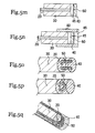
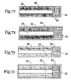
- the heat conduction member 50 may, for example, be disposed between the light guide member 20 and the wavelength conversion member 40 as shown in FIGS. 2a, 2c, 2d, 3f to 3h, and 6s, or may be disposed on the opposite side of the wavelength conversion member 40 from the light guide member 20 as shown in FIGS. 3e, 8bb, and 8cc, or may be disposed so as to cover all or part of the surrounding part (the outer surface) of the wavelength conversion member 40 as shown in FIGS. 2b, 3g, 41, 6t, 7v to 7z, and 9ff to 9ii, or two or more heat conduction members 50 may be disposed via the wavelength conversion member 40 as shown in FIGS.
- the heat conduction member 50 may also be in the form of a mesh.
- the heat conduction member 50 may be disposed only between the wavelength conversion member 40 and the covering member 30 as shown in FIGS. 6r and 6u, or the heat conduction member 50 may be made up of a translucent material and a reflective material from the light guide member 20 to the covering member 30 as shown in FIG. 6s.
- the heat conduction member 50 may be disposed so as to be sandwiched by a plurality of covering members 30. Further, the heat conduction member 50 may be disposed as shown in FIGS. 9ff to 9ii, without the covering member 30 being provided.
- the heat conduction member 50 can be in the form of a convex lens as shown in FIG. 3f, or in the form of a concave lens as shown in FIG. 2c and 3h.
- the contact surface area between the heat conduction member 50 and the wavelength conversion member 40 and/or the covering member 30 is especially favorable because heat dissipation efficiency will be higher. It is also preferable for the configuration to be such that the heat conduction member 50 diffuses the light from the light guide member 20, as shown in FIG. 2c, etc., in which the heat conduction member 50 is a concave lens. This results in light of higher density from the light guide member 20 being incident on the wavelength conversion member 40 after first being diffused, rather than being incident directly, so less light is focussed on the wavelength conversion member 40, and degradation and discoloration of the wavelength conversion member 40 can be effectively reduced.
- the light guide member 20 Since the light guide member 20 is slender enough to be bendable, it has a relatively small diameter and light is more readily focussed. Therefore, a configuration in which the heat conduction member 50 diffuses light from the light guide member 20 is particularly effective when a bendable light guide member 20 is used. Also, as shown in FIG. 6s, the maximum heat dissipation characteristics can be attained, without lowering the output of light from the light emitting element, by disposing a translucent material at the light guide member 20 and a material with high thermal conductivity and reflectivity such as silver or another such metal) at the covering member 30.
- heat dissipation can be further enhanced with the light emitting device of the present invention by disposing a metallic reflector, a wavelength conversion member supporting member, or other such second covering member 60 so as to be thermally connected with the heat conduction member 50.
- the heat conduction member 50 is a convex lens, a concave lens, or any other desired form
- the area around the glass, resin, or the like can be covered with a material such as ITO to produce the heat conduction member 50.
- a material such as ITO to produce the heat conduction member 50.
- the covering of the material constituting the heat conduction member 50 can be accomplished by a known method, such as sputtering, vapor deposition, or plating.
- the following methods are particularly favorable for disposing the heat conduction member 50 on just the outer surface of the covering member 30 as shown in FIGS. 6r and 6u.
- the end face on the emission side of the light guide member 20 and the covering member 30 attached to the end part on the emission side of the light guide member 20 are coated with a resist 70.
- the resist may be heating after this coating.
- the resist 70 is then developed with an alkali solution and rinsed with water. This results in a pattern in which the resist 70 remains only at the emission-side end part of the light guide member 20.
- a metal film is formed over the entire surface of the covering member 30 including the remaining resist 70, and the heat conduction member 50 consisting of the metal film is formed by lift-off on the surface of the covering member 30 other than the emission-side end part of the light guide member 20, as shown in FIG. 13f.
- a negative resist is favorable, but a positive resist may be used instead, and inverted exposure or another such method employed. Also, drying, ashing, or the like may be performed in the course of developing and rinsing with water.
- the heat conduction member may be formed as a plating film on the outer surface of the covering member 30 composed of an electroconductive material.
- a mask 80 is formed so as to cover the portion of the covering member 30 that does not require plating.
- the covering member 30 is fixed to a fixing member 81.
- the covering member 30 is preferably immersed in an ethanol solution 82 and subjected to ultrasonic degreasing and cleaning. This allows the plating of the surface of the covering member 30 to be performed more precisely.
- the surface of the covering member 30 is subjected as desired to strike plating.
- the covering member 30 and a nickel electrode 83 are immersed in a dilute hydrochloric acid solution, and current is supplied. This forms a metal film 50a on just the surface of the covering member 30 composed of the electroconductive material. This strike plating improves the quality of the plating film.
- the surface of the covering member 30 is plated as shown in FIG. 14d.
- the covering member 30 and a silver electrode 85 are immersed in a dilute alkali solution 86, and current is supplied.
- this forms a main plating film 50b over the metal film 50a produced by strike plating, and the metal film 50a and the plating film 50b can be formed as the heat conduction member 50.
- a translucent heat conduction material film may be formed on just the end face of the light guide member 20 by the above-mentioned lift-off method or the like, thereby forming the heat conduction member shown in FIG. 6s.
- the thickness of the heat conduction member 50 there are no restrictions on the thickness of the heat conduction member 50 as long as this member contributes to heat dissipation, but a thickness of about 1 to 100 ⁇ m, for example, is favorable.
- the light emitting device in this embodiment mainly comprises the light emitting element 10, the light guide member 20, the covering member 30, the wavelength conversion member 40, and the heat conduction member 50.
- a lens 2 for converging light 1 from the light emitting element 10 is provided on the front face of the light emitting element 10.
- An LD composed of a GaN (gallium nitride)-based semiconductor having an emission peak wavelength near 445 nm is used as the light emitting element 10
- a quartz SI-type optical fiber (core diameter of 114 ⁇ m, cladding diameter of 125 ⁇ m) is used as the light guide member 20
- the covering member 30 is composed of alumina and had a diameter of 0.7 mm
- the wavelength conversion member 40 comprises two kinds of fluorescent material, namely, 0.53 g of Lu 3 Al 5 O 12 :Ce (emits green light) and 0.2 g of (Sr,Ca) 2 Si 5 N 8 :Eu (emits red light), contained in 1.1 g of silicone resin
- AlN film thickness of 0.1 mm
- the wavelength conversion member 40 is formed by potting.
- the light emitting device in this embodiment is the same as in Embodiment 1 except that the heat conduction member 50 was formed from ITO.
- the ITO was formed by sputtering.
- an embodiment of the present invention can be a light emitting device in which two or more of the units shown in FIG. 1 are combined.
- the wavelength conversion member 40 and the heat conduction member 50 both to be constituted by a single member.
- the light that is ultimately obtained is not limited to white light, and can instead be green light, for instance.
- an LD composed of a GaN (gallium nitride)-based semiconductor having an emission peak wavelength near 405 nm was used as the light emitting element 10
- a heat conduction member 50 composed of ITO (film thickness of 300 nm) was sandwiched between glass and the wavelength conversion member 40.
- the ITO was formed by sputtering.
- the thickness of the wavelength conversion member 40 was about 500 ⁇ m, for example.
- the fluorescent substance was a mixture of 10 g of Ca 10 (PO 4 ) 6 Cl 2 :Eu (emits blue light), 100 g of isopropyl alcohol, 20 g of alumina sol, and 10 g of acetone, a voltage of 50 V was applied to this, and then the fluorescent substance was dried and electrodeposited to form the wavelength conversion member 40.
- a light emitting device was formed by the same method as above, except that no heat conduction member 50 composed of ITO was provided.
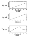
- FIG. 10a shows the results of baking CCA
- FIG. 10b the electrodeposition of CCA
- FIG. 10c the baking of CCA in a comparative example.
- FIGS. 10a and 10b It can be seen from FIGS. 10a and 10b that with the light emitting device of this embodiment, providing the heat conduction member 50 yields extremely good linearity between the light output (at the end of the light guide member 20) and the relative intensity of the light flux. In other words, it can be seen that degradation of the wavelength conversion member 40 by heat can be greatly reduced, and that the result is a reliable light emitting device of high light output. Meanwhile, as shown in FIG. 10c, when no heat conduction member 50 was provided, extremely good linearity was not obtained between the light output and the relative intensity of the light flux, and degradation of the wavelength conversion member occurred.
- an LD composed of a GaN (gallium nitride)-based semiconductor having an emission peak wavelength near 445 nm was used as the light emitting element 10, and a heat conduction member 50 composed of ITO (film thickness of 300 nm) was sandwiched between glass and the wavelength conversion member 40.
- the ITO was formed by sputtering.
- the wavelength conversion member 40 was formed from just a fluorescent material by electrodeposition in the same manner as in Embodiment 3, except that (Y,Gd) 3 Al 5 O 12 :Ce (YAG) was used.
- a light emitting device was formed by the same method as above, except that no heat conduction member 50 composed of ITO was provided, and the YAG was baked by the same method as in Embodiment 3.
- the light emitting device of this embodiment has substantially the same constitution as the light emitting device of Embodiment 1, except that, as a modification of FIG. 5o, a plurality of (such as seven or 14) wire-shaped heat conduction members 50 were provided not protruding into the wavelength conversion member, as shown in FIG. 12b.
- the light guide member was an SI-type optical fiber made of silver-plated quartz.
- the wavelength conversion member 40 was formed by potting, using a mixture of Lu 3 Al 5 O 12 :Ce (LAG) and Ca 0.99 AlSiB 0.10 N 3.1 :Eu 0.01 (CASBN) in a silicone resin.
- the wire-shaped heat conduction members 50 consisted of tin-plated soft steel with a diameter of 160 ⁇ m.
- a light emitting device was formed with the same constitution as above, except that no wire-shaped heat conduction members 50 were provided.
- a light emitting device embodying the present invention can be utilized in indicators, displays, and various kinds of lighting, such as lighting installed in automobiles. It can also be utilized in fiber scopes that allow illumination of narrow gaps and dark spaces, in endoscopes for imaging the inside of the body, and so forth.
Abstract
Description
- The present invention relates to a light emitting device having a light emitting element, a light guide member, and a wavelength conversion member.
- There has long been a need for a light emitting device with which color information can be accurately reproduced at high output. The use of light emitting diodes (hereinafter referred to as LEDs), laser diodes (hereinafter referred to as LDs), and other such light emitting elements as the light source for such devices has already been proposed (see, for example,
WO01/040702 - LEDs and LDs are compact, have good power efficiency, emit light in vivid colors, and eliminate problems such as broken bulbs. In particular, LDs have higher optical density than LEDs, so a light emitting device of higher brightness can be obtained.
- Nevertheless, with the LEDs, LDs, and so forth discussed in
WO01/040702 - Accordingly, it is desirable to provide a light emitting device with high output and a long service life.
- According to an embodiment of the present invention there is provided a light emitting device, comprising at least: a light emitting element; a wavelength conversion member for converting the wavelength of light from the light emitting element; a bendable light guide member for guiding light from the light emitting element to the wavelength conversion member; and a heat conduction member that is thermally connected to the wavelength conversion member.
-
- FIG. 1 is a simplified overall diagram of a light emitting device embodying the present invention;
- FIGS. 2 to 4 are simplified diagrams of the cross sectional structure near the distal end in the light emitting device embodying the present invention;
- FIG. 5 shows simplified diagrams of the cross sectional and oblique structure near the distal end in the light emitting device embodying the present invention;
- FIGS. 6 to 9 are simplified diagrams of the cross sectional structure near the distal end in the light emitting device embodying the present invention;
- FIGS. 10 to 12 are graphs of the output characteristics in working and comparative examples of the light emitting device embodying the present invention; and
- FIGS. 13 and 14 are simplified diagrams illustrating some of the steps involved in manufacturing the light emitting device embodying the present invention.
- A light emitting device embodying the present invention will now be described through reference to the drawings. However, the light emitting devices discussed below are merely given to embody the technological concept of the present invention, and the present invention is not limited thereto. Unless otherwise specified, the dimensions, materials, shapes, relative layouts, and so forth of the constituent members are nothing more than illustrative examples, and should not be construed to limit the scope of the present invention to just these. Furthermore, the sizes, positional relationships, and so forth of the members shown in the drawings may be exaggerated in order to clarify the description. In addition, the elements that make up an embodiment of the present invention may be such that a plurality of elements are constituted by a single member, or conversely, a single element may be constituted by a plurality of members.
- FIG. 1 is a simplified overall diagram of a light emitting device embodying the present invention, and FIG. 2 is a simplified diagram of the detailed structured near the distal end of the light emitting device embodying the present invention. As shown in FIGS. 1 and 2, the light emitting device embodying the present invention is made up primarily of a
light emitting element 10, alight guide member 20, awavelength conversion member 40, and aheat conduction member 50 that is thermally connected to thewavelength conversion member 40. This allows heat generated in thewavelength conversion member 40 by light from thelight emitting element 10 to be effectively taken away by theheat conduction member 50, and mitigates the degradation and discoloration caused by heat to thewavelength conversion member 40 and its peripheral members. - In this Specification, the phrase "thermally connected" does not necessarily mean that one member is directly and completely connected physically to another member. For instance, one member may be indirectly connected with another member via yet another member, or one member may be partially in contact with another member.
- There are no particular restrictions on the
light emitting element 10, but an LD or LED can be used favorably. Using one of these affords a light emitting device with excellent initial drive characteristics, good durability in terms of vibration and repeated on/off flashing, a compact size, and high light emission output. - In particular, since an LD has higher optical density than an LED, the use of an LD allows the brightness of the light emitting device to be easily increased, but this same high optical density also means that the
wavelength conversion member 40 will be more apt to generate heat that can lead to degradation and discoloration. An embodiment of the present invention can greatly reduce the adverse effect of heat from thewavelength conversion member 40, and is therefore particularly effective when an LD is used as thelight emitting element 10. - The
light guide member 20 is designed to be bendable and to extend in the lengthwise direction. This allows light to be easily guided to the desired location. Thelight guide member 20 preferably has a circular cross section, but is not limited to this. There are no particular restrictions on the diameter of thelight guide member 20, but it can be 3000 µm or less, 1000 µm or less, 400 µm or less, or even 200 µm or less. When the cross section is not circular, the "diameter" of thelight guide member 20 refers to the average diameter in the cross section. - The
light emitting element 10 is disposed at one end of thelight guide member 20, and thewavelength conversion member 40 is disposed at the other end. There are no particular restrictions on thelight guide member 20, as long as it guides light from thelight emitting element 10 to thewavelength conversion member 40, but an optical fiber can be used to advantage. An optical fiber is preferable because it can guide light from the light emitting element very efficiently. An optical fiber is usually configured such that a core with a high refractive index is disposed on the inside, and cladding with a low refractive index is disposed on the outside. There are no particular restrictions on the shape of the end of thelight guide member 20 on thelight emitting element 10 side and/or the end on the wavelength conversion member 40 (discussed below) side, and any of various shapes can be employed, such as a flat surface, a convex lens, a concave lens, or a shape in which bumps are provided in at least some portion. For instance, when thelight guide member 20 is an optical fiber, the core and/or cladding at the ends can have one of the above-mentioned shapes. - The light emitting device embodying the present invention can be equipped with a covering
member 30. The coveringmember 30 covers at least part of the side face of thelight guide member 20, and preferably the side face of (that is, around) the emission-side end. Providing the coveringmember 30 allows thewavelength conversion member 40, the heat conduction member 50(discussed below), and so forth to be disposed more easily. - When the light emitting device embodying the present invention is equipped with the covering
member 30, the coveringmember 30 is preferably connected thermally to thewavelength conversion member 40 via aheat conduction member 50. This allows heat generated by thewavelength conversion member 40 to be more effectively radiated to the coveringmember 30, which mitigates the adverse effects of heat from thewavelength conversion member 40. Here, if the thermal conductivity of the coveringmember 30 is made to be higher than the thermal conductivity of thewavelength conversion member 40, degradation and discoloration of thewavelength conversion member 40 caused by heat can be more effectively reduced. - The covering
member 30 is preferably formed from a material that has either high thermal conductivity, or a high optical refractive index, or a high reflectivity with respect to excited light from the light emitting element and/or light that has undergone wavelength conversion (discussed below), or a material that has two or more of these properties. An example of such a material is one whose reflectivity is at least 80% with respect to excited light and/or light that has undergone wavelength conversion, whose refractive index is at least n:1.4 with respect to light of about 350 to 500 nm, and/or whose thermal conductivity is at least 0.1 W/m·°C. - The covering
member 30 can, for example, be made of silver (Ag), aluminum (Al), copper (Cu), nickel (Ni), silicon carbide (SiC), zirconia (ZrO2), alumina (Al2O3), aluminum nitride (AlN), barium sulfate (BaSO4), carbon, stainless steel, borosilicate glass, or the like. Of these, zirconia is preferable because it has high reflectivity and is easy to work. Furthermore, because alumina has high thermal conductivity and high reflectivity over the entire visible light spectrum, it is particularly favorable when the light emitting device is one that emits white light. - A light reflecting film may be disposed on the side of the covering
member 30 where thewavelength conversion member 40 is disposed, or specific bumps may be formed on this side so that light is scattered. As a result, when light from the light emitting element and/or light that has undergone wavelength conversion is returned by reflection to thelight guide member 20 side, it can be re-reflected by the coveringmember 30, and light from the light emitting element and/or light that has undergone wavelength conversion can be taken off to the outside more effectively. The side having the light reflecting film and/or bumps need not be provided to just the coveringmember 30, but may also be provided to at least part of the emission end of thelight guide member 20. - Also, the covering
member 30 need not necessarily be a single member, and a combination of a plurality of members of various shapes may be used (see FIG. 8aa, for example). In this case, the coveringmember 30 can be given the function of supporting thelight guide member 20 and thewavelength conversion member 40, or the function of a reflector for reflecting light, or the function of sandwiching a heat conduction member (discussed below) in between members. - The
wavelength conversion member 40 converts the wavelength of light from thelight emitting element 10, and may, for example, be made up solely of a fluorescent material, or a fluorescent material may be contained in a translucent member such as an epoxy resin, silicone resin, or other such organic material, or a low-melting point glass, crystalline glass, or other such inorganic material. In particular, when a translucent member made of an organic material is used, since this member.will be susceptible to degradation by light, an embodiment of the present invention is particularly effective when the translucent member is made of an organic material. - The
wavelength conversion member 40 absorbs at least part of the light from thelight emitting element 10, converts the wavelength to a different wavelength band, and emits light having an emission spectrum in the red band, the green band, the blue band, etc. There are no particular restrictions on the type of fluorescent material, as long as it will at least convert the wavelength of light from the light emitting element, and various kinds can be used. With the light emitting device embodying the present invention, for example, light from thelight emitting element 10 can be mixed with light from one or more fluorescent materials, or light from two or more fluorescent materials can be mixed, allowing a white color to be obtained. To obtain better color rendering, it is preferable to use a material with which the average color rendering index (Ra) of incident light will be at least 70, with at least 80 being even better. - The
wavelength conversion member 40 can contain SiO2 or another such filler as desired in an embodiment of the present invention. A filler serves to reflect and scatter incident light. This results in better color mixing and reduces color unevenness. Also, mixing a filler into thewavelength conversion member 40 allows the viscosity thereof to be adjusted, so it can be more easily disposed in thelight guide member 20, the coveringmember 30, and theheat conduction member 50. - The
wavelength conversion member 40 may consist of a first layer constituted by an inorganic member containing a fluorescent material, a second layer constituted by an organic member containing the same or a different type of fluorescent material as the fluorescent material contained in the first layer, and so forth, disposed in that order starting from thelight emitting element 10 side. This reduces degradation of the first layer, which is nearer to thelight emitting element 10 that is relatively more prone to degradation, and as a result increases the service life of the light emitting device. A translucent member that does not contain a fluorescent material may also be used in combination at the desired location within the wavelength conversion member. For instance, thewavelength conversion member 40 shown in FIGS. 2a to 9ii may be partially formed solely from a translucent member that does not contain a fluorescent material. - In general, some of the light will not undergo wavelength conversion and will become heat. With an embodiment of the present invention, because the portion where the light is guided to the wavelength conversion member is extremely narrow, there is pronounced concentration of light in the wavelength conversion member, and the attendant generation of heat, but the degradation and discoloration of the
wavelength conversion member 40 can be effectively reduced even in this situation with a light emitting device embodying the present invention. - The
heat conduction member 50 absorbs the heat produced by thewavelength conversion member 40, and also reduces the generation of heat in thewavelength conversion member 40. Also, it is preferably translucent so that at least part of the light from thelight emitting element 10 and/or light that has undergone wavelength conversion will be transmitted. This allows light from thelight emitting element 10 and/or light that has undergone wavelength conversion to be taken off from efficiently. There are no particular restrictions on the material constituting theheat conduction member 50, but one whose thermal conductivity is at least about 0.1 w/m·k is preferable, with at least about 0.5 w/m·k being even better. From another standpoint, it is preferable to use a material whose thermal conductivity is better than that of the organic member or inorganic member used in the wavelength conversion member. For example, aluminum nitride (AlN), silicon carbide (SiC), CuW, CuMO, Cu diamond, diamond, a transparent electroconductive material (such as indium tin oxide (ITO), indium oxide (In2O3), zinc oxide (ZnO), tin oxide (SnO2), or magnesium oxide (MgO)), or the like can be used, either singly or in combination. Aluminum nitride is particularly favorable because it has relatively high thermal conductivity and is easy to mold into a light emitting device. - The
heat conduction member 50 may, for example, be disposed between thelight guide member 20 and thewavelength conversion member 40 as shown in FIGS. 2a, 2c, 2d, 3f to 3h, and 6s, or may be disposed on the opposite side of thewavelength conversion member 40 from thelight guide member 20 as shown in FIGS. 3e, 8bb, and 8cc, or may be disposed so as to cover all or part of the surrounding part (the outer surface) of thewavelength conversion member 40 as shown in FIGS. 2b, 3g, 41, 6t, 7v to 7z, and 9ff to 9ii, or two or moreheat conduction members 50 may be disposed via thewavelength conversion member 40 as shown in FIGS. 2d and 4i, or may be disposed between thewavelength conversion member 40 and a translucent member as shown in FIGS. 5m and 5n, or may be disposed in a concentric circular or cup shape in thewavelength conversion member 40 as shown in FIGS. 4j and 4k, or may be disposed in the form of rods or bent rods (the more, the better) in thewavelength conversion member 40 as shown in FIGS. 5o to 5q. Theheat conduction member 50 may also be in the form of a mesh. Theheat conduction member 50 may be disposed only between thewavelength conversion member 40 and the coveringmember 30 as shown in FIGS. 6r and 6u, or theheat conduction member 50 may be made up of a translucent material and a reflective material from thelight guide member 20 to the coveringmember 30 as shown in FIG. 6s. - From another standpoint, as shown in FIGS. 8aa to 8ee, the
heat conduction member 50 may be disposed so as to be sandwiched by a plurality of coveringmembers 30. Further, theheat conduction member 50 may be disposed as shown in FIGS. 9ff to 9ii, without the coveringmember 30 being provided. - Also, the
heat conduction member 50 can be in the form of a convex lens as shown in FIG. 3f, or in the form of a concave lens as shown in FIG. 2c and 3h. - It is especially favorable for the contact surface area between the
heat conduction member 50 and thewavelength conversion member 40 and/or the coveringmember 30 to be as large as possible because heat dissipation efficiency will be higher. It is also preferable for the configuration to be such that theheat conduction member 50 diffuses the light from thelight guide member 20, as shown in FIG. 2c, etc., in which theheat conduction member 50 is a concave lens. This results in light of higher density from thelight guide member 20 being incident on thewavelength conversion member 40 after first being diffused, rather than being incident directly, so less light is focussed on thewavelength conversion member 40, and degradation and discoloration of thewavelength conversion member 40 can be effectively reduced. Since thelight guide member 20 is slender enough to be bendable, it has a relatively small diameter and light is more readily focussed. Therefore, a configuration in which theheat conduction member 50 diffuses light from thelight guide member 20 is particularly effective when a bendablelight guide member 20 is used. Also, as shown in FIG. 6s, the maximum heat dissipation characteristics can be attained, without lowering the output of light from the light emitting element, by disposing a translucent material at thelight guide member 20 and a material with high thermal conductivity and reflectivity such as silver or another such metal) at the coveringmember 30. - As shown in FIGS. 2h, 5n, and 8aa to 8ee, heat dissipation can be further enhanced with the light emitting device of the present invention by disposing a metallic reflector, a wavelength conversion member supporting member, or other such
second covering member 60 so as to be thermally connected with theheat conduction member 50. - When the
heat conduction member 50 is a convex lens, a concave lens, or any other desired form, the area around the glass, resin, or the like can be covered with a material such as ITO to produce theheat conduction member 50. This allows theheat conduction member 50 to be produced in the desired form with relative ease. The covering of the material constituting theheat conduction member 50 can be accomplished by a known method, such as sputtering, vapor deposition, or plating. - The following methods are particularly favorable for disposing the
heat conduction member 50 on just the outer surface of the coveringmember 30 as shown in FIGS. 6r and 6u. - First, as shown in FIG. 13a, the end face on the emission side of the
light guide member 20 and the coveringmember 30 attached to the end part on the emission side of thelight guide member 20 are coated with a resist 70. The resist may be heating after this coating. - Next, as shown in FIG. 13b, light is allowed to propagate through the
light guide member 20 to expose the resist 70 covering the emission-side end face of thelight guide member 20. With this method, just the desired portion of the resist 70 can be exposed at high precision, without having to perform mask alignment (see FIG. 13c). - The resist 70 is then developed with an alkali solution and rinsed with water. This results in a pattern in which the resist 70 remains only at the emission-side end part of the
light guide member 20. - After this, as shown in FIG. 13e, a metal film is formed over the entire surface of the covering
member 30 including the remaining resist 70, and theheat conduction member 50 consisting of the metal film is formed by lift-off on the surface of the coveringmember 30 other than the emission-side end part of thelight guide member 20, as shown in FIG. 13f. - With this process, the use of a negative resist is favorable, but a positive resist may be used instead, and inverted exposure or another such method employed. Also, drying, ashing, or the like may be performed in the course of developing and rinsing with water.
- As another method, as shown in FIG. 14a, the heat conduction member may be formed as a plating film on the outer surface of the covering
member 30 composed of an electroconductive material. - First, a
mask 80 is formed so as to cover the portion of the coveringmember 30 that does not require plating. - Next, as shown in FIG. 14b, the covering
member 30 is fixed to a fixingmember 81. The coveringmember 30 is preferably immersed in anethanol solution 82 and subjected to ultrasonic degreasing and cleaning. This allows the plating of the surface of the coveringmember 30 to be performed more precisely. - Next, as shown in FIG. 14c, the surface of the covering
member 30 is subjected as desired to strike plating. For example, the coveringmember 30 and anickel electrode 83 are immersed in a dilute hydrochloric acid solution, and current is supplied. This forms ametal film 50a on just the surface of the coveringmember 30 composed of the electroconductive material. This strike plating improves the quality of the plating film. - Next, the surface of the covering
member 30 is plated as shown in FIG. 14d. For example, the coveringmember 30 and asilver electrode 85 are immersed in adilute alkali solution 86, and current is supplied. As shown in FIG. 14e, this forms amain plating film 50b over themetal film 50a produced by strike plating, and themetal film 50a and theplating film 50b can be formed as theheat conduction member 50. - After this, if desired, a translucent heat conduction material film may be formed on just the end face of the
light guide member 20 by the above-mentioned lift-off method or the like, thereby forming the heat conduction member shown in FIG. 6s. - There are no restrictions on the thickness of the
heat conduction member 50 as long as this member contributes to heat dissipation, but a thickness of about 1 to 100 µm, for example, is favorable. - Embodiments of the present invention will now be described.
- The light emitting device in this embodiment, as shown in FIGS. 1 and 2a, mainly comprises the
light emitting element 10, thelight guide member 20, the coveringmember 30, thewavelength conversion member 40, and theheat conduction member 50. Alens 2 for converging light 1 from thelight emitting element 10 is provided on the front face of thelight emitting element 10. - An LD composed of a GaN (gallium nitride)-based semiconductor having an emission peak wavelength near 445 nm is used as the
light emitting element 10, a quartz SI-type optical fiber (core diameter of 114 µm, cladding diameter of 125 µm) is used as thelight guide member 20, the coveringmember 30 is composed of alumina and had a diameter of 0.7 mm, thewavelength conversion member 40 comprises two kinds of fluorescent material, namely, 0.53 g of Lu3Al5O12:Ce (emits green light) and 0.2 g of (Sr,Ca)2Si5N8:Eu (emits red light), contained in 1.1 g of silicone resin, and AlN (film thickness of 0.1 mm) is used as theheat conduction member 50. Thewavelength conversion member 40 is formed by potting. - With this light emitting device, degradation of the
wavelength conversion member 40 by heat is greatly reduced as compared to a light emitting device not equipped with theheat conduction member 50. As a result, a reliable light emitting device of high emission output can be obtained. - The light emitting device in this embodiment, as shown in FIG. 2e, is the same as in
Embodiment 1 except that theheat conduction member 50 was formed from ITO. The ITO was formed by sputtering. - With this light emitting device, degradation of the
wavelength conversion member 40 by heat is greatly reduced as compared to a light emitting device not equipped with theheat conduction member 50. As a result, a reliable light emitting device of high emission output can be obtained. - Furthermore, an embodiment of the present invention can be a light emitting device in which two or more of the units shown in FIG. 1 are combined. In this case, it is preferable for the
wavelength conversion member 40 and theheat conduction member 50 both to be constituted by a single member. Also, the light that is ultimately obtained is not limited to white light, and can instead be green light, for instance. - With the light emitting device in this embodiment, as shown in FIG. 5m, an LD composed of a GaN (gallium nitride)-based semiconductor having an emission peak wavelength near 405 nm was used as the
light emitting element 10, and aheat conduction member 50 composed of ITO (film thickness of 300 nm) was sandwiched between glass and thewavelength conversion member 40. The ITO was formed by sputtering. - The
wavelength conversion member 40 was formed by mixing as fluorescent substances 2 g of Ca10(PO4)6Cl2:Eu (emits blue light) with 2 g of a liquid mixture of ethyl cellulose and terpineol (weight ratio = 12:88), and sintering this mixture for 30 minutes at 80°C, 10 minutes at 200°C, and 1 hour at 500°C to bake the fluorescent substance. The thickness of thewavelength conversion member 40 was about 500 µm, for example. - Alternatively, the fluorescent substance was a mixture of 10 g of Ca10(PO4)6Cl2:Eu (emits blue light), 100 g of isopropyl alcohol, 20 g of alumina sol, and 10 g of acetone, a voltage of 50 V was applied to this, and then the fluorescent substance was dried and electrodeposited to form the
wavelength conversion member 40. - For the sake of comparison, a light emitting device was formed by the same method as above, except that no
heat conduction member 50 composed of ITO was provided. - The light output characteristics of the light emitting devices thus obtained were measured, the results of which are given in FIGS. 10a to 10c. FIG. 10a shows the results of baking CCA, FIG. 10b the electrodeposition of CCA, and FIG. 10c the baking of CCA in a comparative example.
- It can be seen from FIGS. 10a and 10b that with the light emitting device of this embodiment, providing the
heat conduction member 50 yields extremely good linearity between the light output (at the end of the light guide member 20) and the relative intensity of the light flux. In other words, it can be seen that degradation of thewavelength conversion member 40 by heat can be greatly reduced, and that the result is a reliable light emitting device of high light output. Meanwhile, as shown in FIG. 10c, when noheat conduction member 50 was provided, extremely good linearity was not obtained between the light output and the relative intensity of the light flux, and degradation of the wavelength conversion member occurred. - With the light emitting device in this embodiment, as shown in FIG. 5m, an LD composed of a GaN (gallium nitride)-based semiconductor having an emission peak wavelength near 445 nm was used as the
light emitting element 10, and aheat conduction member 50 composed of ITO (film thickness of 300 nm) was sandwiched between glass and thewavelength conversion member 40. The ITO was formed by sputtering. - The
wavelength conversion member 40 was formed from just a fluorescent material by electrodeposition in the same manner as in Embodiment 3, except that (Y,Gd)3Al5O12:Ce (YAG) was used. - For the sake of comparison, a light emitting device was formed by the same method as above, except that no
heat conduction member 50 composed of ITO was provided, and the YAG was baked by the same method as in Embodiment 3. - The light output characteristics of the light emitting devices thus obtained were measured, the results of which are given in FIGS. 11a and 11b.
- It can be seen from FIG. 11b that with the light emitting device of this embodiment, providing the
heat conduction member 50 yields extremely good linearity between the light output and the relative intensity of the light flux. In other words, it can be seen that degradation of thewavelength conversion member 40 by heat can be greatly reduced, and that the result is a reliable light emitting device of high light output. Meanwhile, as shown in FIG. 11a, when noheat conduction member 50 was provided, extremely good linearity was not obtained between the light output and the relative intensity of the light flux, and degradation of the wavelength conversion member occurred. - The light emitting device of this embodiment has substantially the same constitution as the light emitting device of
Embodiment 1, except that, as a modification of FIG. 5o, a plurality of (such as seven or 14) wire-shapedheat conduction members 50 were provided not protruding into the wavelength conversion member, as shown in FIG. 12b. - The light guide member was an SI-type optical fiber made of silver-plated quartz. The
wavelength conversion member 40 was formed by potting, using a mixture of Lu3Al5O12:Ce (LAG) and Ca0.99AlSiB0.10N3.1:Eu0.01 (CASBN) in a silicone resin. - The wire-shaped
heat conduction members 50 consisted of tin-plated soft steel with a diameter of 160 µm. - For the sake of comparison, a light emitting device was formed with the same constitution as above, except that no wire-shaped
heat conduction members 50 were provided. - The light output characteristics of the light emitting devices thus obtained were measured, the results of which are given in FIG. 12a.
- It can be seen from FIG. 12a that as the number of wire-shaped heat conduction members was increased from zero (dashed line) to seven (one-dot chain line) and then to 14 (solid line), the degradation of the
wavelength conversion member 40 by heat was greatly reduced, and as a result a larger light output could be obtained. - A light emitting device embodying the present invention can be utilized in indicators, displays, and various kinds of lighting, such as lighting installed in automobiles. It can also be utilized in fiber scopes that allow illumination of narrow gaps and dark spaces, in endoscopes for imaging the inside of the body, and so forth.
- This application claims priority to
Japanese Patent Application Nos. 2005-172220 2006-129332 Japanese Patent Application Nos. 2005-172220 2006-129332 - While only selected embodiments have been chosen to illustrate the present invention, it will be apparent to those skilled in the art from this disclosure that various changes and modifications can be made herein without departing from the scope of the invention as defined in the appended claims. Furthermore, the foregoing description of the embodiments according to the present invention are provided for illustration only, and not for the purpose of limiting the invention as defined by the appended claims and their equivalents.
Claims (6)
- A light emitting device, comprising at least:a light emitting element;a wavelength conversion member for converting the wavelength of light from the light emitting element;a bendable light guide member for guiding light from the light emitting element to the wavelength conversion member; anda heat conduction member that is thermally connected to the wavelength conversion member.
- The light emitting device according to Claim 1, further comprising a covering member that covers at least part of the side face of the light guide member,
wherein the covering member and the wavelength conversion member are thermally connected via the heat conduction member. - The light emitting element according to Claim 1 or 2, wherein the wavelength conversion member is made up of at least a translucent member and a fluorescent material.
- The light emitting device according to Claim 1, 2 or 3, wherein the light emitting element is a laser diode, and
the light guide member is an optical fiber. - The light emitting device according to any preceding Claim, wherein the heat conduction member is composed of a material having a thermal conductivity of at least 0.1 w/m·k.
- The light emitting device according to any of Claims 2 to 5, wherein the covering member is composed of an electroconductive material, and the heat conduction member is composed of a plating film formed on all or part of the outer surface of the covering member.
Priority Applications (1)
| Application Number | Priority Date | Filing Date | Title |
|---|---|---|---|
| EP08101041.5A EP1921477B1 (en) | 2005-06-13 | 2006-06-13 | A light emitting device |
Applications Claiming Priority (2)
| Application Number | Priority Date | Filing Date | Title |
|---|---|---|---|
| JP2005172220 | 2005-06-13 | ||
| JP2006129332A JP5124978B2 (en) | 2005-06-13 | 2006-05-08 | Light emitting device |
Related Child Applications (2)
| Application Number | Title | Priority Date | Filing Date |
|---|---|---|---|
| EP08101041.5A Division-Into EP1921477B1 (en) | 2005-06-13 | 2006-06-13 | A light emitting device |
| EP08101041.5A Division EP1921477B1 (en) | 2005-06-13 | 2006-06-13 | A light emitting device |
Publications (2)
| Publication Number | Publication Date |
|---|---|
| EP1734302A1 true EP1734302A1 (en) | 2006-12-20 |
| EP1734302B1 EP1734302B1 (en) | 2017-07-26 |
Family
ID=36939116
Family Applications (2)
| Application Number | Title | Priority Date | Filing Date |
|---|---|---|---|
| EP06253028.2A Active EP1734302B1 (en) | 2005-06-13 | 2006-06-13 | A light emitting device |
| EP08101041.5A Active EP1921477B1 (en) | 2005-06-13 | 2006-06-13 | A light emitting device |
Family Applications After (1)
| Application Number | Title | Priority Date | Filing Date |
|---|---|---|---|
| EP08101041.5A Active EP1921477B1 (en) | 2005-06-13 | 2006-06-13 | A light emitting device |
Country Status (4)
| Country | Link |
|---|---|
| US (1) | US7422356B2 (en) |
| EP (2) | EP1734302B1 (en) |
| JP (1) | JP5124978B2 (en) |
| CN (1) | CN1880833B (en) |
Cited By (17)
| Publication number | Priority date | Publication date | Assignee | Title |
|---|---|---|---|---|
| WO2008058612A1 (en) * | 2006-11-14 | 2008-05-22 | Storz Endoskop Produktions Gmbh | Endoscopic system featuring fiber-pumped fluorescent illumination |
| EP2042898A1 (en) | 2007-09-28 | 2009-04-01 | OSRAM Opto Semiconductors GmbH | Light source with conversion element and fibre optic cable, method for producing light source and its application |
| DE102008012316A1 (en) | 2007-09-28 | 2009-04-02 | Osram Opto Semiconductors Gmbh | Semiconductor light source with a primary radiation source and a luminescence conversion element |
| DE102008011866A1 (en) | 2008-02-29 | 2009-09-10 | Osram Opto Semiconductors Gmbh | Semiconductor light source for light source arrangement of projector, has reflector element guiding primary radiation on luminescence material or deflects secondary radiation delivered from material in direction of primary radiation source |
| DE102008046523A1 (en) | 2008-09-10 | 2010-03-11 | Osram Opto Semiconductors Gmbh | Lamp has semiconductor laser element which is designed to emit primary radiation with wavelength between two hundred nanometer and five hundred nanometer |
| DE102008049922A1 (en) * | 2008-10-02 | 2010-04-08 | Karl Storz Gmbh & Co. Kg | endoscope |
| WO2010085414A1 (en) * | 2009-01-21 | 2010-07-29 | Alcon Research, Ltd. | Ophthalmic endoillumination using fiber generated light |
| DE102010001945A1 (en) | 2010-02-15 | 2011-08-18 | Osram Gesellschaft mit beschränkter Haftung, 81543 | Light source unit for use in projector, has cooling device representing cooling body whose surface area is applied with phosphor, aluminum and silver, and mirror coupled between excitation beam sources and optical collimation device |
| US8488930B2 (en) | 2010-12-09 | 2013-07-16 | Alcon Research, Ltd. | Wavelength converting illumination probe |
| DE102013206338A1 (en) * | 2013-04-10 | 2014-10-16 | Osram Gmbh | lighting device |
| EP2822111A1 (en) * | 2013-07-03 | 2015-01-07 | Nichia Corporation | Light emitting device |
| EP2777482A4 (en) * | 2011-11-10 | 2015-07-08 | Fujifilm Corp | Illumination optics unit for endoscope and method for producing same |
| US20150345728A1 (en) | 2013-02-18 | 2015-12-03 | Koito Manufacturing Co., Ltd. | Automotive lamp |
| EP2713410B1 (en) * | 2012-09-27 | 2018-05-02 | Stanley Electric Co., Ltd. | Light emitting device |
| RU2665332C1 (en) * | 2013-11-19 | 2018-08-29 | Филипс Лайтинг Холдинг Б.В. | Light-emitting device with spectral transformation element |
| EP3489326A1 (en) * | 2009-04-09 | 2019-05-29 | Signify Holding B.V. | Lamp for laser applications |
| WO2019162147A1 (en) * | 2018-02-20 | 2019-08-29 | Lumileds Holding B.V. | Light converting device with confined light converter |
Families Citing this family (86)
| Publication number | Priority date | Publication date | Assignee | Title |
|---|---|---|---|---|
| EP1795798B1 (en) * | 2004-10-01 | 2013-07-03 | Nichia Corporation | Light-emitting device |
| US7846391B2 (en) | 2006-05-22 | 2010-12-07 | Lumencor, Inc. | Bioanalytical instrumentation using a light source subsystem |
| JP4946188B2 (en) * | 2006-06-13 | 2012-06-06 | 日亜化学工業株式会社 | Light emitting device |
| US7618176B2 (en) * | 2006-06-22 | 2009-11-17 | Avago Technologies General Ip (Singapore) Pte. Ltd. | Solid state light source adapted for remote illumination |
| JP2008235439A (en) * | 2007-03-19 | 2008-10-02 | Nec Lighting Ltd | White light source device |
| JP2008245668A (en) * | 2007-03-29 | 2008-10-16 | Fujinon Corp | Imaging apparatus of electronic endoscope and electronic endoscope |
| US8409081B2 (en) * | 2007-04-27 | 2013-04-02 | Olympus Medical Systems Corp. | Illumination light application structure and endoscope provided with the same |
| JP5162955B2 (en) * | 2007-05-10 | 2013-03-13 | 日亜化学工業株式会社 | Semiconductor light emitting device |
| US8098375B2 (en) | 2007-08-06 | 2012-01-17 | Lumencor, Inc. | Light emitting diode illumination system |
| JP5019289B2 (en) * | 2007-08-10 | 2012-09-05 | オリンパス株式会社 | Fiber optic lighting equipment |
| DE102007041439A1 (en) * | 2007-08-28 | 2009-03-05 | Carl Zeiss Surgical Gmbh | Secondary light source |
| JP5173663B2 (en) * | 2008-08-07 | 2013-04-03 | オリンパス株式会社 | LIGHT SOURCE DEVICE AND ENDOSCOPE DEVICE USING THE SAME |
| JP5571889B2 (en) * | 2008-08-29 | 2014-08-13 | 株式会社東芝 | Light emitting device and lighting device |
| JP2010081957A (en) * | 2008-09-29 | 2010-04-15 | Olympus Corp | Light source device |
| WO2010049875A1 (en) * | 2008-10-30 | 2010-05-06 | Koninklijke Philips Electronics N.V. | Laser lighting device |
| JP2010123819A (en) * | 2008-11-21 | 2010-06-03 | Shimadzu Corp | Laser medium |
| US8242462B2 (en) | 2009-01-23 | 2012-08-14 | Lumencor, Inc. | Lighting design of high quality biomedical devices |
| JP5384970B2 (en) * | 2009-02-25 | 2014-01-08 | オリンパス株式会社 | Adapter type endoscope |
| DE102009017940A1 (en) * | 2009-04-17 | 2010-10-21 | Storz Endoskop Produktions Gmbh | Endoscopic system |
| JP5066134B2 (en) * | 2009-05-28 | 2012-11-07 | 株式会社東芝 | Optical wiring cable |
| JP2011029432A (en) * | 2009-07-27 | 2011-02-10 | Sharp Corp | Light-emitting device and lighting device with the same |
| US8714769B2 (en) * | 2009-09-16 | 2014-05-06 | Sight Saver, Llc | Light system |
| JP5478232B2 (en) * | 2009-12-11 | 2014-04-23 | オリンパス株式会社 | Lighting device |
| JP4991834B2 (en) | 2009-12-17 | 2012-08-01 | シャープ株式会社 | Vehicle headlamp |
| JP5519303B2 (en) * | 2010-01-20 | 2014-06-11 | オリンパス株式会社 | Wavelength conversion unit and lighting device including the same |
| JP5232815B2 (en) * | 2010-02-10 | 2013-07-10 | シャープ株式会社 | Vehicle headlamp |
| DE102010028949A1 (en) * | 2010-05-12 | 2011-11-17 | Osram Gesellschaft mit beschränkter Haftung | headlight module |
| US8733996B2 (en) | 2010-05-17 | 2014-05-27 | Sharp Kabushiki Kaisha | Light emitting device, illuminating device, and vehicle headlamp |
| CN102313166B (en) * | 2010-05-17 | 2015-01-14 | 夏普株式会社 | Light emitting element, light emitting device, illuminating device, and vehicle headlamp |
| JP5255018B2 (en) * | 2010-05-17 | 2013-08-07 | シャープ株式会社 | Laser downlight and laser downlight system |
| EP2585758A2 (en) | 2010-06-23 | 2013-05-01 | Sight Saver LLC | Attachable illumination system |
| JP2012016545A (en) * | 2010-07-09 | 2012-01-26 | Fujifilm Corp | Endoscope apparatus |
| GB201012764D0 (en) * | 2010-07-30 | 2010-09-15 | Element Six N V | A diamond window component for a laser tool |
| JP2012059454A (en) * | 2010-09-07 | 2012-03-22 | Sharp Corp | Light emitting device, lighting system, and headlamp for vehicle |
| JP5425024B2 (en) * | 2010-09-07 | 2014-02-26 | シャープ株式会社 | Vehicle headlamp |
| US8833975B2 (en) | 2010-09-07 | 2014-09-16 | Sharp Kabushiki Kaisha | Light-emitting device, illuminating device, vehicle headlamp, and method for producing light-emitting device |
| JP5425023B2 (en) * | 2010-09-07 | 2014-02-26 | シャープ株式会社 | Light emitting device, lighting device, and vehicle headlamp |
| JP5549539B2 (en) * | 2010-10-28 | 2014-07-16 | 日本電気硝子株式会社 | Wavelength conversion element, light source including the same, and manufacturing method thereof |
| US9816677B2 (en) | 2010-10-29 | 2017-11-14 | Sharp Kabushiki Kaisha | Light emitting device, vehicle headlamp, illumination device, and laser element |
| JP2012119193A (en) | 2010-12-01 | 2012-06-21 | Sharp Corp | Light-emitting device, vehicular headlamp, lighting device, and vehicle |
| US8389957B2 (en) | 2011-01-14 | 2013-03-05 | Lumencor, Inc. | System and method for metered dosage illumination in a bioanalysis or other system |
| US8466436B2 (en) | 2011-01-14 | 2013-06-18 | Lumencor, Inc. | System and method for metered dosage illumination in a bioanalysis or other system |
| JP2012182376A (en) * | 2011-03-02 | 2012-09-20 | Stanley Electric Co Ltd | Wavelength conversion member and light source device |
| WO2012121343A1 (en) * | 2011-03-08 | 2012-09-13 | シャープ株式会社 | Light-emitting device, illumination device, vehicle headlight, projector, and method for manufacturing light-emitting device |
| JP5021089B1 (en) * | 2011-06-21 | 2012-09-05 | シャープ株式会社 | LIGHT EMITTING DEVICE, LIGHTING DEVICE, VEHICLE HEADLAMP, PROJECTOR, AND LIGHT EMITTING DEVICE MANUFACTURING METHOD |
| WO2012133632A1 (en) * | 2011-03-30 | 2012-10-04 | オリンパス株式会社 | Light source unit, optical conversion unit, light source device, and light source system |
| JP5868629B2 (en) * | 2011-08-02 | 2016-02-24 | オリンパス株式会社 | Light source device |
| JP2013048792A (en) * | 2011-08-31 | 2013-03-14 | Fujifilm Corp | Endoscopic device |
| US8622593B2 (en) | 2011-11-03 | 2014-01-07 | Sight Saver, Llc | Ratchet clip |
| JP5809933B2 (en) * | 2011-11-07 | 2015-11-11 | オリンパス株式会社 | Light source device |
| US9103528B2 (en) | 2012-01-20 | 2015-08-11 | Lumencor, Inc | Solid state continuous white light source |
| US9217561B2 (en) | 2012-06-15 | 2015-12-22 | Lumencor, Inc. | Solid state light source for photocuring |
| DE102012109088B4 (en) * | 2012-09-26 | 2019-05-09 | Schott Ag | Fiber optic conversion module |
| JP6102696B2 (en) * | 2012-12-11 | 2017-03-29 | 日亜化学工業株式会社 | LIGHT EMITTING DEVICE AND METHOD FOR PRODUCING OPTICAL COMPONENT USED FOR THE SAME |
| JP2014187224A (en) * | 2013-03-25 | 2014-10-02 | Stanley Electric Co Ltd | Semiconductor light-emitting device |
| US10386559B2 (en) | 2013-03-29 | 2019-08-20 | Signify Holding B.V. | Light emitting device comprising wavelength converter |
| JP2015005439A (en) * | 2013-06-21 | 2015-01-08 | スタンレー電気株式会社 | Vehicle headlamp and optical fiber bundle used in vehicle headlamp |
| WO2014203484A1 (en) * | 2013-06-21 | 2014-12-24 | パナソニックIpマネジメント株式会社 | Wavelength conversion member, light source and vehicle headlamp |
| DE102013217319A1 (en) * | 2013-08-30 | 2015-03-05 | Osram Gmbh | lighting device |
| SE538234C2 (en) * | 2013-10-18 | 2016-04-12 | Optoskand Ab | Optoelectronic connector |
| JP6428249B2 (en) * | 2013-12-25 | 2018-11-28 | 日亜化学工業株式会社 | Light emitting device |
| DE102014100723A1 (en) * | 2014-01-23 | 2015-07-23 | Hella Kgaa Hueck & Co. | Lighting device for vehicles |
| EP3117267B1 (en) * | 2014-03-11 | 2018-05-02 | Osram Sylvania Inc. | Light converter assemblies with enhanced heat dissipation |
| EP3136942A4 (en) * | 2014-04-29 | 2018-01-17 | Boston Scientific Scimed, Inc. | Lumen-less illumination system |
| JP2016225581A (en) * | 2015-06-04 | 2016-12-28 | 日本電気硝子株式会社 | Wavelength conversion member and light-emitting device including the same |
| JP6250594B2 (en) * | 2015-06-16 | 2017-12-20 | シャープ株式会社 | Light emitting device and lighting device |
| JP6604473B2 (en) * | 2015-10-09 | 2019-11-13 | パナソニックIpマネジメント株式会社 | Lighting apparatus and lighting device |
| US10941924B2 (en) | 2015-12-15 | 2021-03-09 | Wangs Alliance Corporation | LED lighting methods and apparatus |
| US11686459B2 (en) | 2015-12-15 | 2023-06-27 | Wangs Alliance Corporation | LED lighting methods and apparatus |
| US10330294B2 (en) | 2015-12-15 | 2019-06-25 | Wangs Alliance Corporation | LED lighting methods and apparatus |
| CN109416169A (en) * | 2016-03-15 | 2019-03-01 | 飞利浦照明控股有限公司 | Light-emitting device |
| KR102525592B1 (en) * | 2016-04-25 | 2023-05-03 | 엘지이노텍 주식회사 | Lighting apparatus |
| JP6935990B2 (en) * | 2016-06-16 | 2021-09-15 | 株式会社小糸製作所 | Manufacturing method of wavelength conversion member, light emitting device and wavelength conversion member |
| JP6765053B2 (en) * | 2016-07-28 | 2020-10-07 | パナソニックIpマネジメント株式会社 | Light emitting device and light emitting device system |
| WO2018056157A1 (en) * | 2016-09-21 | 2018-03-29 | パナソニックIpマネジメント株式会社 | Wavelength conversion device and iilluminating device |
| JP6848582B2 (en) * | 2017-03-24 | 2021-03-24 | 日本電気硝子株式会社 | Wavelength conversion member and light emitting device |
| JP6861364B2 (en) * | 2017-05-02 | 2021-04-21 | パナソニックIpマネジメント株式会社 | Optical equipment |
| US11812525B2 (en) | 2017-06-27 | 2023-11-07 | Wangs Alliance Corporation | Methods and apparatus for controlling the current supplied to light emitting diodes |
| DE102018107523A1 (en) | 2018-03-29 | 2019-10-02 | Schott Ag | Light or image guide components for disposable endoscopes |
| DE102019133042A1 (en) | 2019-12-04 | 2021-06-10 | Schott Ag | Endoscope, single-use endoscope system and light source for endoscope |
| US11598517B2 (en) | 2019-12-31 | 2023-03-07 | Lumien Enterprise, Inc. | Electronic module group |
| CN110985903B (en) | 2019-12-31 | 2020-08-14 | 江苏舒适照明有限公司 | Lamp module |
| DE102020106915A1 (en) | 2020-03-13 | 2021-09-16 | Schott Ag | Endoscope and single-use endoscope system |
| CN111503556B (en) | 2020-04-23 | 2020-11-27 | 江苏舒适照明有限公司 | Spotlight structure |
| JP7104346B2 (en) | 2020-10-09 | 2022-07-21 | 日亜化学工業株式会社 | Luminescent device |
| US11802682B1 (en) | 2022-08-29 | 2023-10-31 | Wangs Alliance Corporation | Modular articulating lighting |
Citations (13)
| Publication number | Priority date | Publication date | Assignee | Title |
|---|---|---|---|---|
| US4572609A (en) | 1981-07-10 | 1986-02-25 | Agency Of Industrial Science & Technology | Cooling mechanism for optical fiber |
| US4678273A (en) | 1983-12-23 | 1987-07-07 | Radians Ab | High power optical fiber with improved covering |
| US4695697A (en) | 1985-12-13 | 1987-09-22 | Gv Medical, Inc. | Fiber tip monitoring and protection assembly |
| JPH0843659A (en) * | 1994-07-29 | 1996-02-16 | Bridgestone Corp | Optical transmission tube |
| WO2001040702A1 (en) * | 1999-12-03 | 2001-06-07 | Cree Lighting Company | Solid state lamp |
| US6260614B1 (en) | 2000-04-17 | 2001-07-17 | The Boeing Company | Fiber optic bundle interstitial cooling using heat pipe technology |
| WO2003021329A2 (en) | 2001-08-31 | 2003-03-13 | Smith & Nephew, Inc. | Solid-state light source |
| US20040095970A1 (en) | 1995-06-02 | 2004-05-20 | Kazuhisa Yamamoto | Optical device, laser beam source, laser apparatus and method of producing optical device |
| US20050031281A1 (en) | 2003-08-09 | 2005-02-10 | Gunther Nath | Illumination device with light guide and light diffuser |
| US20050084229A1 (en) * | 2003-10-20 | 2005-04-21 | Victor Babbitt | Light insertion and dispersion system |
| JP2005205195A (en) * | 2003-12-22 | 2005-08-04 | Nichia Chem Ind Ltd | Light emitting device and endoscopic system |
| JP2005328921A (en) * | 2004-05-18 | 2005-12-02 | Olympus Corp | Endoscope apparatus and adapter for endoscope |
| EP1605199A2 (en) * | 2004-06-04 | 2005-12-14 | LumiLeds Lighting U.S., LLC | Remote wavelength conversion in an illumination device |
Family Cites Families (18)
| Publication number | Priority date | Publication date | Assignee | Title |
|---|---|---|---|---|
| US4693556A (en) * | 1985-06-04 | 1987-09-15 | Laser Therapeutics, Inc. | Apparatus for producing a spherical pattern of light and method of manufacture |
| US5370649A (en) * | 1991-08-16 | 1994-12-06 | Myriadlase, Inc. | Laterally reflecting tip for laser transmitting fiber |
| JP3971342B2 (en) * | 1995-06-02 | 2007-09-05 | 松下電器産業株式会社 | Laser light source and laser projection apparatus |
| TW383508B (en) * | 1996-07-29 | 2000-03-01 | Nichia Kagaku Kogyo Kk | Light emitting device and display |
| JPH10154830A (en) * | 1996-09-27 | 1998-06-09 | Nichia Chem Ind Ltd | Light emitting device and display device using the same |
| US6396864B1 (en) * | 1998-03-13 | 2002-05-28 | Jds Uniphase Corporation | Thermally conductive coatings for light emitting devices |
| JP2000357406A (en) * | 1999-06-16 | 2000-12-26 | Koken:Kk | Light decoration device |
| JP3721040B2 (en) * | 2000-02-28 | 2005-11-30 | 日本電信電話株式会社 | Fiber-type optical device and manufacturing method thereof |
| JP2002176224A (en) * | 2000-12-07 | 2002-06-21 | Fuji Photo Film Co Ltd | Laser beam source |
| JP4028550B2 (en) * | 2002-09-10 | 2007-12-26 | 古河電気工業株式会社 | Wavelength conversion module |
| JP2004252423A (en) * | 2003-01-31 | 2004-09-09 | Fuji Photo Film Co Ltd | Fiber module and manufacturing method therefor |
| JP2005005544A (en) * | 2003-06-13 | 2005-01-06 | Sumitomo Electric Ind Ltd | White light emitting element |
| JP2005049416A (en) * | 2003-07-30 | 2005-02-24 | Noritsu Koki Co Ltd | Laser system and wavelength transducer |
| JP2005332989A (en) | 2004-05-20 | 2005-12-02 | Topcon Corp | Laser oscillator |
| JP4925618B2 (en) | 2004-07-28 | 2012-05-09 | 京セラ株式会社 | Light source device and endoscope provided with the light source device |
| EP1795798B1 (en) * | 2004-10-01 | 2013-07-03 | Nichia Corporation | Light-emitting device |
| US7433115B2 (en) * | 2004-12-15 | 2008-10-07 | Nichia Corporation | Light emitting device |
| EP1672755B1 (en) * | 2004-12-17 | 2015-09-23 | Nichia Corporation | Light emitting device |
-
2006
- 2006-05-08 JP JP2006129332A patent/JP5124978B2/en active Active
- 2006-06-09 US US11/449,719 patent/US7422356B2/en active Active
- 2006-06-09 CN CN2006100917251A patent/CN1880833B/en active Active
- 2006-06-13 EP EP06253028.2A patent/EP1734302B1/en active Active
- 2006-06-13 EP EP08101041.5A patent/EP1921477B1/en active Active
Patent Citations (13)
| Publication number | Priority date | Publication date | Assignee | Title |
|---|---|---|---|---|
| US4572609A (en) | 1981-07-10 | 1986-02-25 | Agency Of Industrial Science & Technology | Cooling mechanism for optical fiber |
| US4678273A (en) | 1983-12-23 | 1987-07-07 | Radians Ab | High power optical fiber with improved covering |
| US4695697A (en) | 1985-12-13 | 1987-09-22 | Gv Medical, Inc. | Fiber tip monitoring and protection assembly |
| JPH0843659A (en) * | 1994-07-29 | 1996-02-16 | Bridgestone Corp | Optical transmission tube |
| US20040095970A1 (en) | 1995-06-02 | 2004-05-20 | Kazuhisa Yamamoto | Optical device, laser beam source, laser apparatus and method of producing optical device |
| WO2001040702A1 (en) * | 1999-12-03 | 2001-06-07 | Cree Lighting Company | Solid state lamp |
| US6260614B1 (en) | 2000-04-17 | 2001-07-17 | The Boeing Company | Fiber optic bundle interstitial cooling using heat pipe technology |
| WO2003021329A2 (en) | 2001-08-31 | 2003-03-13 | Smith & Nephew, Inc. | Solid-state light source |
| US20050031281A1 (en) | 2003-08-09 | 2005-02-10 | Gunther Nath | Illumination device with light guide and light diffuser |
| US20050084229A1 (en) * | 2003-10-20 | 2005-04-21 | Victor Babbitt | Light insertion and dispersion system |
| JP2005205195A (en) * | 2003-12-22 | 2005-08-04 | Nichia Chem Ind Ltd | Light emitting device and endoscopic system |
| JP2005328921A (en) * | 2004-05-18 | 2005-12-02 | Olympus Corp | Endoscope apparatus and adapter for endoscope |
| EP1605199A2 (en) * | 2004-06-04 | 2005-12-14 | LumiLeds Lighting U.S., LLC | Remote wavelength conversion in an illumination device |
Non-Patent Citations (2)
| Title |
|---|
| PATENT ABSTRACTS OF JAPAN vol. 1996, no. 06 28 June 1996 (1996-06-28) * |
| PATENT ABSTRACTS OF JAPAN vol. 2003, no. 12 5 December 2003 (2003-12-05) * |
Cited By (29)
| Publication number | Priority date | Publication date | Assignee | Title |
|---|---|---|---|---|
| WO2008058612A1 (en) * | 2006-11-14 | 2008-05-22 | Storz Endoskop Produktions Gmbh | Endoscopic system featuring fiber-pumped fluorescent illumination |
| DE102006053487B4 (en) * | 2006-11-14 | 2013-12-19 | Storz Endoskop Produktions Gmbh | Endoscopic system with fiber-pumped fluorescence illumination |
| EP2336818A1 (en) * | 2006-11-14 | 2011-06-22 | Storz Endoskop Produktions GmbH | Endoscopic system with fibre-pumped fluorescence illumination |
| US7706053B2 (en) | 2007-09-28 | 2010-04-27 | Osram Opto Semiconductors Gmbh | Light source with conversion element and fiber optics |
| EP2042898A1 (en) | 2007-09-28 | 2009-04-01 | OSRAM Opto Semiconductors GmbH | Light source with conversion element and fibre optic cable, method for producing light source and its application |
| DE102008012316B4 (en) | 2007-09-28 | 2023-02-02 | OSRAM Opto Semiconductors Gesellschaft mit beschränkter Haftung | Semiconductor light source with a primary radiation source and a luminescence conversion element |
| US8564185B2 (en) | 2007-09-28 | 2013-10-22 | Osram Opto Semiconductors Gmbh | Semiconductor light source having a primary radiation source and a luminescence conversion element |
| WO2009039827A1 (en) * | 2007-09-28 | 2009-04-02 | Osram Opto Semiconductors Gmbh | Semiconductor light source having a primary radiation source and a luminescence conversion element |
| DE102008012316A1 (en) | 2007-09-28 | 2009-04-02 | Osram Opto Semiconductors Gmbh | Semiconductor light source with a primary radiation source and a luminescence conversion element |
| DE102008011866A1 (en) | 2008-02-29 | 2009-09-10 | Osram Opto Semiconductors Gmbh | Semiconductor light source for light source arrangement of projector, has reflector element guiding primary radiation on luminescence material or deflects secondary radiation delivered from material in direction of primary radiation source |
| DE102008011866B4 (en) | 2008-02-29 | 2018-05-03 | Osram Opto Semiconductors Gmbh | Light source arrangement with a semiconductor light source |
| DE102008046523A1 (en) | 2008-09-10 | 2010-03-11 | Osram Opto Semiconductors Gmbh | Lamp has semiconductor laser element which is designed to emit primary radiation with wavelength between two hundred nanometer and five hundred nanometer |
| DE102008049922A1 (en) * | 2008-10-02 | 2010-04-08 | Karl Storz Gmbh & Co. Kg | endoscope |
| WO2010085414A1 (en) * | 2009-01-21 | 2010-07-29 | Alcon Research, Ltd. | Ophthalmic endoillumination using fiber generated light |
| US8277048B2 (en) | 2009-01-21 | 2012-10-02 | Alcon Research, Ltd. | Ophthalmic endoillumination using fiber generated light |
| EP3489326A1 (en) * | 2009-04-09 | 2019-05-29 | Signify Holding B.V. | Lamp for laser applications |
| DE102010001945B4 (en) | 2010-02-15 | 2019-07-25 | Osram Gmbh | Light source unit and projector with such a light source unit |
| DE102010001945A1 (en) | 2010-02-15 | 2011-08-18 | Osram Gesellschaft mit beschränkter Haftung, 81543 | Light source unit for use in projector, has cooling device representing cooling body whose surface area is applied with phosphor, aluminum and silver, and mirror coupled between excitation beam sources and optical collimation device |
| US8488930B2 (en) | 2010-12-09 | 2013-07-16 | Alcon Research, Ltd. | Wavelength converting illumination probe |
| EP2777482A4 (en) * | 2011-11-10 | 2015-07-08 | Fujifilm Corp | Illumination optics unit for endoscope and method for producing same |
| EP2713410B1 (en) * | 2012-09-27 | 2018-05-02 | Stanley Electric Co., Ltd. | Light emitting device |
| US20150345728A1 (en) | 2013-02-18 | 2015-12-03 | Koito Manufacturing Co., Ltd. | Automotive lamp |
| EP2957818A4 (en) * | 2013-02-18 | 2016-11-23 | Koito Mfg Co Ltd | Vehicle light fitting |
| US10247381B2 (en) | 2013-02-18 | 2019-04-02 | Koito Manufacturing Co., Ltd. | Automotive lamp |
| DE102013206338A1 (en) * | 2013-04-10 | 2014-10-16 | Osram Gmbh | lighting device |
| EP2822111A1 (en) * | 2013-07-03 | 2015-01-07 | Nichia Corporation | Light emitting device |
| RU2665332C1 (en) * | 2013-11-19 | 2018-08-29 | Филипс Лайтинг Холдинг Б.В. | Light-emitting device with spectral transformation element |
| WO2019162147A1 (en) * | 2018-02-20 | 2019-08-29 | Lumileds Holding B.V. | Light converting device with confined light converter |
| US11420557B2 (en) | 2018-02-20 | 2022-08-23 | Lumileds, LLC | Light converting device with confined light converter |
Also Published As
| Publication number | Publication date |
|---|---|
| CN1880833A (en) | 2006-12-20 |
| JP5124978B2 (en) | 2013-01-23 |
| US7422356B2 (en) | 2008-09-09 |
| EP1734302B1 (en) | 2017-07-26 |
| EP1921477A8 (en) | 2010-06-09 |
| JP2007027688A (en) | 2007-02-01 |
| CN1880833B (en) | 2010-08-25 |
| US20060279950A1 (en) | 2006-12-14 |
| EP1921477B1 (en) | 2014-11-12 |
| EP1921477A2 (en) | 2008-05-14 |
| EP1921477A3 (en) | 2008-06-04 |
Similar Documents
| Publication | Publication Date | Title |
|---|---|---|
| US7422356B2 (en) | Light emitting device | |
| TWI261937B (en) | Light-emitting apparatus and illuminating apparatus | |
| JP4847954B2 (en) | Reflecting member, light emitting device and lighting device using the same | |
| TWI311803B (en) | ||
| JP4946188B2 (en) | Light emitting device | |
| KR100752586B1 (en) | Light-emitting apparatus and illuminating apparatus | |
| JP4698412B2 (en) | Light emitting device and lighting device | |
| JP4983613B2 (en) | Semiconductor light emitting device | |
| JP4688553B2 (en) | Light emitting device and lighting device | |
| JP2008147610A (en) | Light emitting device | |
| JP2008021973A (en) | Light emitting device | |
| JP5109498B2 (en) | Light emitting device | |
| US20140098541A1 (en) | Lighting apparatus | |
| JP2005340472A (en) | Light-emitting device and illuminator | |
| JP2006066657A (en) | Light emitting device and lighting device | |
| JP4935215B2 (en) | Light emitting device | |
| JP5124908B2 (en) | Light emitting device | |
| JP5085851B2 (en) | Light emitting device and lighting device | |
| JP2009049386A (en) | Illuminating light source and illuminator | |
| JP2006093612A (en) | Light emitting device and illuminator | |
| JP5561296B2 (en) | Light emitting device | |
| CN217386124U (en) | Light source device and optical-mechanical system | |
| CN110925625B (en) | Light emitting device | |
| CN116954009A (en) | Light source device and optical-mechanical system | |
| JP2010182880A (en) | Package for mounting light-emitting element |
Legal Events
| Date | Code | Title | Description |
|---|---|---|---|
| PUAI | Public reference made under article 153(3) epc to a published international application that has entered the european phase |
Free format text: ORIGINAL CODE: 0009012 |
|
| AK | Designated contracting states |
Kind code of ref document: A1 Designated state(s): AT BE BG CH CY CZ DE DK EE ES FI FR GB GR HU IE IS IT LI LT LU LV MC NL PL PT RO SE SI SK TR |
|
| AX | Request for extension of the european patent |
Extension state: AL BA HR MK YU |
|
| 17P | Request for examination filed |
Effective date: 20070613 |
|
| AKX | Designation fees paid |
Designated state(s): AT BE BG CH CY CZ DE DK EE ES FI FR GB GR HU IE IS IT LI LT LU LV MC NL PL PT RO SE SI SK TR |
|
| 17Q | First examination report despatched |
Effective date: 20070905 |
|
| REG | Reference to a national code |
Ref country code: DE Ref legal event code: R079 Ref document number: 602006053116 Country of ref document: DE Free format text: PREVIOUS MAIN CLASS: F21V0029000000 Ipc: G02B0006320000 |
|
| GRAP | Despatch of communication of intention to grant a patent |
Free format text: ORIGINAL CODE: EPIDOSNIGR1 |
|
| RIC1 | Information provided on ipc code assigned before grant |
Ipc: G02B 6/32 20060101AFI20170116BHEP Ipc: G02B 6/42 20060101ALI20170116BHEP |
|
| INTG | Intention to grant announced |
Effective date: 20170207 |
|
| GRAC | Information related to communication of intention to grant a patent modified |
Free format text: ORIGINAL CODE: EPIDOSCIGR1 |
|
| INTG | Intention to grant announced |
Effective date: 20170215 |
|
| GRAS | Grant fee paid |
Free format text: ORIGINAL CODE: EPIDOSNIGR3 |
|
| GRAA | (expected) grant |
Free format text: ORIGINAL CODE: 0009210 |
|
| AK | Designated contracting states |
Kind code of ref document: B1 Designated state(s): AT BE BG CH CY CZ DE DK EE ES FI FR GB GR HU IE IS IT LI LT LU LV MC NL PL PT RO SE SI SK TR |
|
| REG | Reference to a national code |
Ref country code: GB Ref legal event code: FG4D |
|
| REG | Reference to a national code |
Ref country code: CH Ref legal event code: EP |
|
| REG | Reference to a national code |
Ref country code: AT Ref legal event code: REF Ref document number: 912836 Country of ref document: AT Kind code of ref document: T Effective date: 20170815 |
|
| REG | Reference to a national code |
Ref country code: IE Ref legal event code: FG4D |
|
| REG | Reference to a national code |
Ref country code: DE Ref legal event code: R096 Ref document number: 602006053116 Country of ref document: DE |
|
| REG | Reference to a national code |
Ref country code: NL Ref legal event code: MP Effective date: 20170726 |
|
| REG | Reference to a national code |
Ref country code: LT Ref legal event code: MG4D |
|
| REG | Reference to a national code |
Ref country code: AT Ref legal event code: MK05 Ref document number: 912836 Country of ref document: AT Kind code of ref document: T Effective date: 20170726 |
|
| PG25 | Lapsed in a contracting state [announced via postgrant information from national office to epo] |
Ref country code: AT Free format text: LAPSE BECAUSE OF FAILURE TO SUBMIT A TRANSLATION OF THE DESCRIPTION OR TO PAY THE FEE WITHIN THE PRESCRIBED TIME-LIMIT Effective date: 20170726 Ref country code: FI Free format text: LAPSE BECAUSE OF FAILURE TO SUBMIT A TRANSLATION OF THE DESCRIPTION OR TO PAY THE FEE WITHIN THE PRESCRIBED TIME-LIMIT Effective date: 20170726 Ref country code: SE Free format text: LAPSE BECAUSE OF FAILURE TO SUBMIT A TRANSLATION OF THE DESCRIPTION OR TO PAY THE FEE WITHIN THE PRESCRIBED TIME-LIMIT Effective date: 20170726 Ref country code: NL Free format text: LAPSE BECAUSE OF FAILURE TO SUBMIT A TRANSLATION OF THE DESCRIPTION OR TO PAY THE FEE WITHIN THE PRESCRIBED TIME-LIMIT Effective date: 20170726 Ref country code: LT Free format text: LAPSE BECAUSE OF FAILURE TO SUBMIT A TRANSLATION OF THE DESCRIPTION OR TO PAY THE FEE WITHIN THE PRESCRIBED TIME-LIMIT Effective date: 20170726 |
|
| PG25 | Lapsed in a contracting state [announced via postgrant information from national office to epo] |
Ref country code: PL Free format text: LAPSE BECAUSE OF FAILURE TO SUBMIT A TRANSLATION OF THE DESCRIPTION OR TO PAY THE FEE WITHIN THE PRESCRIBED TIME-LIMIT Effective date: 20170726 Ref country code: BG Free format text: LAPSE BECAUSE OF FAILURE TO SUBMIT A TRANSLATION OF THE DESCRIPTION OR TO PAY THE FEE WITHIN THE PRESCRIBED TIME-LIMIT Effective date: 20171026 Ref country code: GR Free format text: LAPSE BECAUSE OF FAILURE TO SUBMIT A TRANSLATION OF THE DESCRIPTION OR TO PAY THE FEE WITHIN THE PRESCRIBED TIME-LIMIT Effective date: 20171027 Ref country code: LV Free format text: LAPSE BECAUSE OF FAILURE TO SUBMIT A TRANSLATION OF THE DESCRIPTION OR TO PAY THE FEE WITHIN THE PRESCRIBED TIME-LIMIT Effective date: 20170726 Ref country code: IS Free format text: LAPSE BECAUSE OF FAILURE TO SUBMIT A TRANSLATION OF THE DESCRIPTION OR TO PAY THE FEE WITHIN THE PRESCRIBED TIME-LIMIT Effective date: 20171126 Ref country code: ES Free format text: LAPSE BECAUSE OF FAILURE TO SUBMIT A TRANSLATION OF THE DESCRIPTION OR TO PAY THE FEE WITHIN THE PRESCRIBED TIME-LIMIT Effective date: 20170726 |
|
| PG25 | Lapsed in a contracting state [announced via postgrant information from national office to epo] |
Ref country code: CZ Free format text: LAPSE BECAUSE OF FAILURE TO SUBMIT A TRANSLATION OF THE DESCRIPTION OR TO PAY THE FEE WITHIN THE PRESCRIBED TIME-LIMIT Effective date: 20170726 Ref country code: DK Free format text: LAPSE BECAUSE OF FAILURE TO SUBMIT A TRANSLATION OF THE DESCRIPTION OR TO PAY THE FEE WITHIN THE PRESCRIBED TIME-LIMIT Effective date: 20170726 Ref country code: RO Free format text: LAPSE BECAUSE OF FAILURE TO SUBMIT A TRANSLATION OF THE DESCRIPTION OR TO PAY THE FEE WITHIN THE PRESCRIBED TIME-LIMIT Effective date: 20170726 |
|
| REG | Reference to a national code |
Ref country code: DE Ref legal event code: R097 Ref document number: 602006053116 Country of ref document: DE |
|
| REG | Reference to a national code |
Ref country code: FR Ref legal event code: PLFP Year of fee payment: 13 |
|
| PG25 | Lapsed in a contracting state [announced via postgrant information from national office to epo] |
Ref country code: IT Free format text: LAPSE BECAUSE OF FAILURE TO SUBMIT A TRANSLATION OF THE DESCRIPTION OR TO PAY THE FEE WITHIN THE PRESCRIBED TIME-LIMIT Effective date: 20170726 Ref country code: SK Free format text: LAPSE BECAUSE OF FAILURE TO SUBMIT A TRANSLATION OF THE DESCRIPTION OR TO PAY THE FEE WITHIN THE PRESCRIBED TIME-LIMIT Effective date: 20170726 Ref country code: EE Free format text: LAPSE BECAUSE OF FAILURE TO SUBMIT A TRANSLATION OF THE DESCRIPTION OR TO PAY THE FEE WITHIN THE PRESCRIBED TIME-LIMIT Effective date: 20170726 |
|
| PLBE | No opposition filed within time limit |
Free format text: ORIGINAL CODE: 0009261 |
|
| STAA | Information on the status of an ep patent application or granted ep patent |
Free format text: STATUS: NO OPPOSITION FILED WITHIN TIME LIMIT |
|
| 26N | No opposition filed |
Effective date: 20180430 |
|
| PG25 | Lapsed in a contracting state [announced via postgrant information from national office to epo] |
Ref country code: SI Free format text: LAPSE BECAUSE OF FAILURE TO SUBMIT A TRANSLATION OF THE DESCRIPTION OR TO PAY THE FEE WITHIN THE PRESCRIBED TIME-LIMIT Effective date: 20170726 |
|
| REG | Reference to a national code |
Ref country code: CH Ref legal event code: PL |
|
| REG | Reference to a national code |
Ref country code: BE Ref legal event code: MM Effective date: 20180630 |
|
| REG | Reference to a national code |
Ref country code: IE Ref legal event code: MM4A |
|
| PG25 | Lapsed in a contracting state [announced via postgrant information from national office to epo] |
Ref country code: MC Free format text: LAPSE BECAUSE OF FAILURE TO SUBMIT A TRANSLATION OF THE DESCRIPTION OR TO PAY THE FEE WITHIN THE PRESCRIBED TIME-LIMIT Effective date: 20170726 Ref country code: LU Free format text: LAPSE BECAUSE OF NON-PAYMENT OF DUE FEES Effective date: 20180613 |
|
| PG25 | Lapsed in a contracting state [announced via postgrant information from national office to epo] |
Ref country code: CH Free format text: LAPSE BECAUSE OF NON-PAYMENT OF DUE FEES Effective date: 20180630 Ref country code: IE Free format text: LAPSE BECAUSE OF NON-PAYMENT OF DUE FEES Effective date: 20180613 Ref country code: LI Free format text: LAPSE BECAUSE OF NON-PAYMENT OF DUE FEES Effective date: 20180630 |
|
| PG25 | Lapsed in a contracting state [announced via postgrant information from national office to epo] |
Ref country code: BE Free format text: LAPSE BECAUSE OF NON-PAYMENT OF DUE FEES Effective date: 20180630 |
|
| PG25 | Lapsed in a contracting state [announced via postgrant information from national office to epo] |
Ref country code: TR Free format text: LAPSE BECAUSE OF FAILURE TO SUBMIT A TRANSLATION OF THE DESCRIPTION OR TO PAY THE FEE WITHIN THE PRESCRIBED TIME-LIMIT Effective date: 20170726 |
|
| PG25 | Lapsed in a contracting state [announced via postgrant information from national office to epo] |
Ref country code: HU Free format text: LAPSE BECAUSE OF FAILURE TO SUBMIT A TRANSLATION OF THE DESCRIPTION OR TO PAY THE FEE WITHIN THE PRESCRIBED TIME-LIMIT; INVALID AB INITIO Effective date: 20060613 Ref country code: PT Free format text: LAPSE BECAUSE OF FAILURE TO SUBMIT A TRANSLATION OF THE DESCRIPTION OR TO PAY THE FEE WITHIN THE PRESCRIBED TIME-LIMIT Effective date: 20170726 |
|
| PG25 | Lapsed in a contracting state [announced via postgrant information from national office to epo] |
Ref country code: CY Free format text: LAPSE BECAUSE OF FAILURE TO SUBMIT A TRANSLATION OF THE DESCRIPTION OR TO PAY THE FEE WITHIN THE PRESCRIBED TIME-LIMIT Effective date: 20170726 |
|
| REG | Reference to a national code |
Ref country code: DE Ref legal event code: R082 Ref document number: 602006053116 Country of ref document: DE Representative=s name: HL KEMPNER PATENTANWAELTE, SOLICITORS (ENGLAND, DE Ref country code: DE Ref legal event code: R082 Ref document number: 602006053116 Country of ref document: DE Representative=s name: HL KEMPNER PATENTANWALT, RECHTSANWALT, SOLICIT, DE |
|
| P01 | Opt-out of the competence of the unified patent court (upc) registered |
Effective date: 20230522 |
|
| PGFP | Annual fee paid to national office [announced via postgrant information from national office to epo] |
Ref country code: FR Payment date: 20230510 Year of fee payment: 18 Ref country code: DE Payment date: 20230502 Year of fee payment: 18 |
|
| PGFP | Annual fee paid to national office [announced via postgrant information from national office to epo] |
Ref country code: GB Payment date: 20230427 Year of fee payment: 18 |