EP1727219A1 - Organic thin film transistor and method for producing the same - Google Patents
Organic thin film transistor and method for producing the same Download PDFInfo
- Publication number
- EP1727219A1 EP1727219A1 EP05104440A EP05104440A EP1727219A1 EP 1727219 A1 EP1727219 A1 EP 1727219A1 EP 05104440 A EP05104440 A EP 05104440A EP 05104440 A EP05104440 A EP 05104440A EP 1727219 A1 EP1727219 A1 EP 1727219A1
- Authority
- EP
- European Patent Office
- Prior art keywords
- electrodes
- pattern
- substrate
- thin film
- minimal distance
- Prior art date
- Legal status (The legal status is an assumption and is not a legal conclusion. Google has not performed a legal analysis and makes no representation as to the accuracy of the status listed.)
- Granted
Links
Images


Classifications
-
- H—ELECTRICITY
- H10—SEMICONDUCTOR DEVICES; ELECTRIC SOLID-STATE DEVICES NOT OTHERWISE PROVIDED FOR
- H10K—ORGANIC ELECTRIC SOLID-STATE DEVICES
- H10K10/00—Organic devices specially adapted for rectifying, amplifying, oscillating or switching; Organic capacitors or resistors having a potential-jump barrier or a surface barrier
- H10K10/80—Constructional details
- H10K10/82—Electrodes
- H10K10/84—Ohmic electrodes, e.g. source or drain electrodes
-
- H—ELECTRICITY
- H10—SEMICONDUCTOR DEVICES; ELECTRIC SOLID-STATE DEVICES NOT OTHERWISE PROVIDED FOR
- H10K—ORGANIC ELECTRIC SOLID-STATE DEVICES
- H10K10/00—Organic devices specially adapted for rectifying, amplifying, oscillating or switching; Organic capacitors or resistors having a potential-jump barrier or a surface barrier
- H10K10/40—Organic transistors
- H10K10/46—Field-effect transistors, e.g. organic thin-film transistors [OTFT]
- H10K10/462—Insulated gate field-effect transistors [IGFETs]
- H10K10/464—Lateral top-gate IGFETs comprising only a single gate
-
- H—ELECTRICITY
- H10—SEMICONDUCTOR DEVICES; ELECTRIC SOLID-STATE DEVICES NOT OTHERWISE PROVIDED FOR
- H10K—ORGANIC ELECTRIC SOLID-STATE DEVICES
- H10K10/00—Organic devices specially adapted for rectifying, amplifying, oscillating or switching; Organic capacitors or resistors having a potential-jump barrier or a surface barrier
- H10K10/40—Organic transistors
- H10K10/46—Field-effect transistors, e.g. organic thin-film transistors [OTFT]
- H10K10/462—Insulated gate field-effect transistors [IGFETs]
- H10K10/468—Insulated gate field-effect transistors [IGFETs] characterised by the gate dielectrics
-
- H—ELECTRICITY
- H10—SEMICONDUCTOR DEVICES; ELECTRIC SOLID-STATE DEVICES NOT OTHERWISE PROVIDED FOR
- H10K—ORGANIC ELECTRIC SOLID-STATE DEVICES
- H10K71/00—Manufacture or treatment specially adapted for the organic devices covered by this subclass
- H10K71/10—Deposition of organic active material
- H10K71/16—Deposition of organic active material using physical vapour deposition [PVD], e.g. vacuum deposition or sputtering
- H10K71/166—Deposition of organic active material using physical vapour deposition [PVD], e.g. vacuum deposition or sputtering using selective deposition, e.g. using a mask
Definitions
- This invention relates to an Organic Thin Film Transistor (OTFT) and a method for producing the same. More specifically, this invention relates to a plurality of Organic Thin Film Transistors which are disposed on a substrate in a matrix-shape for an Active Matrix Display and a method for producing the same.
- OTFT Organic Thin Film Transistor
- OFT Organic Thin Film Transistors
- OTFT comprise an organic material between source electrode and drain electrode whereby the conductivity of the organic material (channel) is controlled by the gate electrode of the OTFT.
- OTFT's are arranged in a matrix vertical and horizontal lines thereby forming a matrix.
- the OTFT's are structured by a method of depositing an array of semiconductor areas (as channels) which overlap the drain and source electrodes.
- the organic semiconductor material will be deposited onto the OTFT substrate (already comprising drain and source electrodes) by using thermal evaporation of organic semiconductor materials through a shadow mask or by using solution based processes for semiconductor materials - printing techniques such as Inkjet printing or Flexo printing or doctor blade coating or other technologies.
- the patterning of the semiconductor layer is essential to achieve a good single transistor performance such as high ON/OFF current ratio.
- the patterning is also required to prevent unwanted cross talk effects between adjacent TFTs and conductive lines in an electronic circuit.
- the non patterned semiconductor material can cause a current leakage path. Therefore the semiconductor material has to be deposited only in the channel area of a single transistor whereby no contact to the channel area of adjacent TFTs shall occur.
- WO 03/098696 A1 (Seiko Epson) describes the fabrication of circuit interconnections in thin film circuits, involving the use of lithographic technique to provide patterned layer and depositing first material at localized regions using inkjet printing technique.
- EP 1 139 455 A2 (Seiko Epson) describes a method of manufacturing an organic EL (electroluminescent) element. A special patterning is required to have an opening corresponding to the region for the formation of an constitutive layer.
- WO 03/056641 A1 (Plastic Logic) describes a method for forming an organic or partly organic switching device, comprising: depositing layers of conducting, semi conducting and/or insulating layers by solution processing and direct printing; defining high-resolution patterns of electro-active polymers by self-aligned formation of a surface energy barrier around a first pattern that repels the solution of a second material.
- OFET organic field-effect transistor
- the improved structuring is obtained by introducing, using a doctor blade, the functional polymer in the mold layer into which recesses are initially produced by an additional step like imprinting.
- US 5,742,129 (Pioneer ) describes a method for manufacturing an organic EL display panel having a plurality of emitting portions surrounded by ramparts and arranged as a matrix.
- the shadow mask is used to deposit the media.
- one object of the invention is to provide a substrate having a plurality of Organic Thin Film Transistors which requires more simple manufacturing techniques in comparison to organic TFT devices of the state of the art.
- Another object of the invention is to provide a method for producing Organic Thin Film Transistors, especially a plurality of Organic Thin Film Transistors arranged on a substrate in a matrix or in a circuit which requires lower costs.
- a further object of the invention is to provide an apparatus capable to produce a plurality of Organic Thin Film Transistors arranged on a substrate at a lower price.
- a substrate having a plurality of thin film transistors each transistor comprising a drain electrode, a source electrode and a channel of semiconducting material between drain electrode and source electrode is provided, whereby the minimal distance between drain electrode and source electrode of one transistor is smaller than the minimal distance between electrodes of adjacent transistors or between electrodes and other conductive lines of the substrate and whereby the channels of semiconducting material of the thin film transistors are formed by a regular pattern of semiconducting material where the maximal dimension of the semiconducting elements of the pattern is smaller than the minimal distance between electrodes of adjacent pairs (or between electrodes and other conductive lines of the substrate) but at least equal to the minimal distance between drain electrode and source electrode of one pair.
- a substrate comprising a plurality of pairs of drain electrodes and source electrodes for thin film transistors whereby the minimal distance between drain electrode and source electrode of one pair is smaller than the minimal distance between electrodes of adjacent pairs or between electrodes and other conductive lines of the substrate, whereby the substrate comprises a regular pattern of semiconducting material where the maximal dimension of the semiconducting elements of the pattern is smaller than the minimal distance between electrodes of adjacent pairs (or between electrodes and other conductive lines of the substrate) but at least equal to the minimal distance between drain electrode and source electrode of one pair.
- the substrate comprises a rectangular shape and the drain electrodes and source electrodes comprise a longish shape where the longitudinal axes of drain electrode and source electrode of one pair are disposed parallel to each other and parallel to one of the edges of the rectangular-shaped substrate.
- the maximal dimension of the semiconducting elements of the pattern is at least 50% bigger than the minimal distance between drain electrode and source electrode of one pair.
- the maximal dimension of the semiconducting elements of the pattern is 100% bigger than the minimal distance between drain electrode and source electrode of one pair.
- the minimal distance between electrodes of adjacent pairs is at least 200% bigger than the minimal distance between drain electrode and source electrode of one pair.
- the substrate having a plurality of TFT's can be manufactured without precise alignment requirements which require complex technology and process time.
- the alignment requirements are only such that the pattern has to be applied in the substrate region, e.g. accuracy in the range of several mm or cm, whereby the alignment requirements according to the state of the art are in the sub-mm range, e.g. in the ⁇ m range.
- the semiconducting elements of the pattern are circular shaped.
- the semiconducting elements of the pattern are arranged in a hexagon shape to each other.
- the advantage of circular-shaped semiconducting elements of the pattern is that simple drops can be applied which can be carried out with low-cost shadow mask processes or printing processes.
- the hexagon-shape arrangement of the elements of the pattern is advantageous because this leads to a very homogeneous distribution of pattern elements for all horizontal and vertical lines of the substrate (which comprise the electrodes and the channels between the electrodes).
- the hexagons of the pattern are tilted by 15° in respect to the longitudinal axes of drain electrodes and source electrodes because such an arrangement results in a superior homogeneous distribution of pattern elements for all horizontal and vertical lines of the substrate.
- a superior homogeneity for horizontal and vertical lines of the substrate can be required for the case in which the plurality of thin film transistors are arranged such that there exist two possible directions for the longitudinal axes of the electrodes which are perpendicular to each other.
- This method for forming the semiconducting channels for a plurality of TFT's requires lower alignment demands and can be therefore carried out faster and at lower costs.
- the main idea of the invention is to form the semiconducting channels by a pattern having such dimensions that in all horizontal and vertical lines of the substrate (which comprise the electrodes and the channels between the electrodes) always sufficient semiconducting material is applied thereby sufficiently connecting all pairs of electrodes of the plurality of TFT's.
- the channels of semiconducting material of the plurality of thin film transistors are formed by applying a hexagon-shaped pattern wherein the semiconducting elements of the pattern are circular shaped.
- the application of the pattern is carried out by deposition of semiconducting material by thermal evaporation through a shadow mask.
- a shadow mask is used which comprises a hexagon-shaped pattern and the shadow mask is arranged such that the hexagons of the shadow mask are tilted by 15° in respect to the longitudinal axes of drain electrodes and source electrodes.
- the invention provides a shadow mask for the application of semiconducting material for a plurality of thin film transistors, whereby the shadow mask comprises hexagon-shaped pattern.
- the shadow mask comprises a rectangular shape where the hexagons of the pattern of the shadow mask are tilted by 15° in respect to one of the edges of the shadow mask.
- the application of the pattern is carried out by printing techniques, preferably inkjet printing techniques.
- a print pattern is used which comprises a hexagon-shaped pattern and the print pattern is arranged such that the hexagons of the pattern are tilted by 15° in respect to the longitudinal axes of drain electrodes and source electrodes.
- the invention provides a print pattern for the application of semiconducting material for a plurality of thin film transistors, whereby the print pattern comprises hexagon-shaped pattern.
- the print pattern comprises a rectangular shape where the hexagons of the pattern of the pattern are tilted by 15° in respect to one of the edges of the hole print pattern.
- Fig. 1 shows a bottom gate Organic Thin Film Transistor in a sectional view which can be used for example for active matrix OLED.
- the Organic Thin Film Transistor comprises a gate electrode 4 (which is disposed on a (ground) substrate 5), an insulator 3, a source electrode 2 and a drain electrode 2a, whereby semiconducting material 1 is disposed between source electrode 2 and drain electrode 2a thereby forming the semiconducting channel 11.
- Fig. 2 shows a top gate Organic Thin Film Transistor in a sectional view which can be used for example for active matrix OLED.
- the Organic Thin Film Transistor comprises a source electrode 2 and a drain electrode 2a (which are disposed on a (ground) substrate 5), whereby semiconducting material 1 is disposed between source electrode 2 and drain electrode 2a thereby forming the semiconducting channel 11.
- An insulator 3 and a gate electrode 4 are disposed upon the electrodes 2, 2a and the channel 11.
- Fig. 3 a) and Fig. 4 a) show the basic principle of the deposition of organic semiconductor material 1 through a shadow mask 13 for the manufacture of a bottom (Fig. 3a) or a top (Fig. 4a) gate Organic Thin Film Transistor in a sectional view.
- the evaporation stream 8 is controlled by the openings of the shadow mask 13 thereby resulting in a deposition of semiconductor material 1 at certain areas (between source electrode 2 and drain electrode 2a).
- a continuous deposition of semiconductor material 1 is not possible because connections between adjacent TFT's have to be avoided. Therefore high alignment requirements for the shadow mask 13 in relation to the substrate 5 exist in order to deposit the semiconductor material 1 (more or less exactly) between source electrode 2 and drain electrode 2a.
- Fig. 3 b) and Fig. 4 b) show the basic principle of the deposition of organic semiconductor material 1 by inkjet printing for the manufacture of a bottom (Fig. 3b) or a top (Fig. 4b) gate Organic Thin Film Transistor in a sectional view.
- the application of semiconductor ink droplets 15 is controlled by the print head 14 thereby resulting in a deposition of semiconductor material 1 at certain areas (between source electrode 2 and drain electrode 2a).
- a continuous deposition of semiconductor material 1 is not possible because connections between adjacent TFT's have to be avoided. Therefore high alignment requirements for the print head 14 in relation to the substrate 5 exist in order to deposit the semiconductor material 1 (more or less exactly) between source electrode 2 and drain electrode 2a.
- the openings of the shadow mask (not shown) have to be precisely positioned over the gaps between source electrodes 2 and drain electrodes 2a for the deposition of the semiconductor material 1.
- the precision is usually in the sub-mm range, for active matrix OLED with high resolution in the ⁇ m range.
- the channel 11 to be filled with semiconductor material 1 comprises a channel Length 16 (L) of the transistor (distance between drain and source electrode) and a channel Width 17 (W) of the transistor.
- Fig. 6 a shows a top view of a section of a substrate 5 comprising two TFT's having source, drain and gate electrode 2, 2a, 4 prior to the application of the semiconducting material 1 (channel 11).
- the minimal distance 16 between drain electrode 2a and source electrode 2 of one pair is smaller than the minimal distance 19 between electrodes 2, 2a of adjacent pairs or between electrodes 2, 2a and other conductive lines (not shown) of the substrate 5, see also Fig. 6 d).
- the manufacture of the preliminary product of Fig. 6a) is known as state of the art.
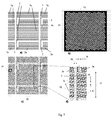
- Fig. 6 b) shows the shadow mask 13 used for the application of the semiconducting material 1 (channel 11).
- the shadow mask 13 comprises a hexagon-shaped pattern 12 and edges 9, 10 wherein the hexagons 21 are tilted by 15° in respect to the longitudinal axis of edge 10 (more precisely shown in Fig. 8).
- Fig. 6 c shows a top view of a section of a substrate 5 comprising two TFT's having source, drain and gate electrode 2, 2a, 4 after the application (deposition) of the semiconducting material 1 (channel 11).
- the substrate 5 now comprises a plurality circular shaped patterned semiconductor areas 6 which result in the pattern 12.
- the diameter 18 of the regularly applied semiconducting elements 6 consisting of semiconducting material 1 is larger than the distance 16 between drain electrode 2a and source electrode 2 of each of the two TFT. Due to the afore-mentioned conditions there always exist semiconducting elements 6 (circular shaped) of pattern 12 which connect drain electrode 2a and source electrode 2 of each TFT.
- the pattern 12 is more precisely shown in Fig. 9.
- the main advantage is that a precise alignment of shadow mask 13 or the print head in relation to the substrate 5 (i.e. in relation to the electrodes 2, 2a of the TFT's) can be avoided. Due to the aforementioned dimensions of 18 and 19 (the distance 19 is larger than 18) there is no unwanted connection between adjacent TFT electrodes or other conductive lines (not shown) via semiconducting material
- Fig. 7 a shows a top view of a section of a substrate 5 comprising several source electrodes 2, drain electrodes 2a and gate electrodes 4 prior to the application of the semiconducting material 1 (channel 11), the gate electrodes not shown being located in the area (channel) between respective pairs of source electrodes 2 and drain electrodes 2a.
- the semiconductor layer for the channel is patterned using new shadow mask 13 design without the need of precise alignment.
- Fig. 7 c) there are many circular shaped patterned semiconductor areas 6 forming the pattern 12 in the final OTFT circuit. There is no unwanted connection path to a neighbour TFT electrodes 2, 2a or other conductive lines because the distance 19 is larger than the dimension 18, see Fig. 7 d).
- the center-to-center distance 20 (N) of neighbouring semiconductor elements 6 is preferably larger than the maximal dimension 18 (D) of the semiconducting elements. Furthermore the channel width 17 (W) of the thin film transistor is preferably larger than the center-to-center distance 20 (N) of neighbouring semiconductor elements 6.
Abstract
Description
- This invention relates to an Organic Thin Film Transistor (OTFT) and a method for producing the same. More specifically, this invention relates to a plurality of Organic Thin Film Transistors which are disposed on a substrate in a matrix-shape for an Active Matrix Display and a method for producing the same.
- Organic Thin Film Transistors (OTFT) comprise an organic material between source electrode and drain electrode whereby the conductivity of the organic material (channel) is controlled by the gate electrode of the OTFT.
- In several applications, e.g. in an Active Matrix Display a plurality of OTFT's are arranged in a matrix vertical and horizontal lines thereby forming a matrix.
In manufacturing processes of OTFT's (arranged in a matrix) the OTFT's are structured by a method of depositing an array of semiconductor areas (as channels) which overlap the drain and source electrodes. The organic semiconductor material will be deposited onto the OTFT substrate (already comprising drain and source electrodes) by using thermal evaporation of organic semiconductor materials through a shadow mask or by using solution based processes for semiconductor materials - printing techniques such as Inkjet printing or Flexo printing or doctor blade coating or other technologies. - The patterning of the semiconductor layer is essential to achieve a good single transistor performance such as high ON/OFF current ratio. The patterning is also required to prevent unwanted cross talk effects between adjacent TFTs and conductive lines in an electronic circuit. The non patterned semiconductor material can cause a current leakage path. Therefore the semiconductor material has to be deposited only in the channel area of a single transistor whereby no contact to the channel area of adjacent TFTs shall occur.
-
WO 03/098696 A1 -
EP 1 139 455 A2 -
US 2003/0059975 A1 andWO 01/46987 A2 -
WO 03/056641 A1 -
DE 100 61 297 A1 (Siemens ) describes an organic field-effect transistor (OFET), a method for structuring an OFET and an integrated circuit with improved structuring of the functional polymer layers. The improved structuring is obtained by introducing, using a doctor blade, the functional polymer in the mold layer into which recesses are initially produced by an additional step like imprinting. -
US 5,946,551 (Dimitrakopoulos et al.) describes the fabrication of TFTs with organic semiconductor. Shadow mask techniques are used to define source/drain metal electrodes. -
US 6,667,215 B2 (3M) describes a method for the manufacture of transistors. Stationary shadow masks are used to define source/drain electrodes. -
US 6,384,529 B2 (Kodak ) describes an color active matrix organic electroluminescent display having an integrated shadow mask. The shadow masks are used to define the color conversion layers or the emissive RGB sub pixels. -
US 5,742,129 (Pioneer ) describes a method for manufacturing an organic EL display panel having a plurality of emitting portions surrounded by ramparts and arranged as a matrix. In the method, the shadow mask is used to deposit the media. There is always a repeated putting and aligning step required to deposit the media through the openings of the shadow mask. - However, all techniques for the deposition of the semiconductor known from the state of the art require a very precise alignment procedure. In case of shadow mask technique a very precise alignment between shadow mask and substrate is required. In case of photolithographic patterned semiconductor, the photomask has to be precisely aligned as well. All printing techniques for the deposition of the semiconductor known from the state of the art require a very precise alignment procedure between printing device and substrate (to be printed). Especially printing processes for flexible substrates require cost intensive local registration during said printing process due to a possible shrinkage of the substrate.
- Therefore one object of the invention is to provide a substrate having a plurality of Organic Thin Film Transistors which requires more simple manufacturing techniques in comparison to organic TFT devices of the state of the art. Another object of the invention is to provide a method for producing Organic Thin Film Transistors, especially a plurality of Organic Thin Film Transistors arranged on a substrate in a matrix or in a circuit which requires lower costs. A further object of the invention is to provide an apparatus capable to produce a plurality of Organic Thin Film Transistors arranged on a substrate at a lower price.
- In one aspect of the invention a substrate having a plurality of thin film transistors, each transistor comprising a drain electrode, a source electrode and a channel of semiconducting material between drain electrode and source electrode is provided, whereby the minimal distance between drain electrode and source electrode of one transistor is smaller than the minimal distance between electrodes of adjacent transistors or between electrodes and other conductive lines of the substrate and whereby the channels of semiconducting material of the thin film transistors are formed by a regular pattern of semiconducting material where the maximal dimension of the semiconducting elements of the pattern is smaller than the minimal distance between electrodes of adjacent pairs (or between electrodes and other conductive lines of the substrate) but at least equal to the minimal distance between drain electrode and source electrode of one pair.
- In another aspect of the invention a substrate comprising a plurality of pairs of drain electrodes and source electrodes for thin film transistors is provided whereby the minimal distance between drain electrode and source electrode of one pair is smaller than the minimal distance between electrodes of adjacent pairs or between electrodes and other conductive lines of the substrate, whereby the substrate comprises a regular pattern of semiconducting material where the maximal dimension of the semiconducting elements of the pattern is smaller than the minimal distance between electrodes of adjacent pairs (or between electrodes and other conductive lines of the substrate) but at least equal to the minimal distance between drain electrode and source electrode of one pair.
- Preferably the substrate comprises a rectangular shape and the drain electrodes and source electrodes comprise a longish shape where the longitudinal axes of drain electrode and source electrode of one pair are disposed parallel to each other and parallel to one of the edges of the rectangular-shaped substrate.
- Preferably the maximal dimension of the semiconducting elements of the pattern is at least 50% bigger than the minimal distance between drain electrode and source electrode of one pair. In a very preferred embodiment of the invention the maximal dimension of the semiconducting elements of the pattern is 100% bigger than the minimal distance between drain electrode and source electrode of one pair.
- Preferably the minimal distance between electrodes of adjacent pairs is at least 200% bigger than the minimal distance between drain electrode and source electrode of one pair.
- By the application of a regular pattern of semiconducting material it is possible to form the semiconducting channels of a plurality of TFT's without the necessity of precise alignment of the used technique because by the above-described dimensions the pattern elements (of semiconducting material) and the distances between source electrode and drain electrode of one pairs (or TFT) and adjacent electrodes (or other conductive lines on the substrate) there will always be a semiconducting material in all horizontal and vertical lines of the substrate connecting the pairs of electrodes thereby forming an TFT (or preliminary product). Therefore the substrate having a plurality of TFT's can be manufactured without precise alignment requirements which require complex technology and process time.
The alignment requirements are only such that the pattern has to be applied in the substrate region, e.g. accuracy in the range of several mm or cm, whereby the alignment requirements according to the state of the art are in the sub-mm range, e.g. in the µm range. - Preferably the semiconducting elements of the pattern are circular shaped. In a very preferred embodiment of the invention the semiconducting elements of the pattern are arranged in a hexagon shape to each other. The advantage of circular-shaped semiconducting elements of the pattern is that simple drops can be applied which can be carried out with low-cost shadow mask processes or printing processes. Furthermore the hexagon-shape arrangement of the elements of the pattern is advantageous because this leads to a very homogeneous distribution of pattern elements for all horizontal and vertical lines of the substrate (which comprise the electrodes and the channels between the electrodes).
- In a preferred embodiment of the invention the hexagons of the pattern are tilted by 15° in respect to the longitudinal axes of drain electrodes and source electrodes because such an arrangement results in a superior homogeneous distribution of pattern elements for all horizontal and vertical lines of the substrate. A superior homogeneity for horizontal and vertical lines of the substrate can be required for the case in which the plurality of thin film transistors are arranged such that there exist two possible directions for the longitudinal axes of the electrodes which are perpendicular to each other.
- According to the invention a method for producing a substrate comprising a plurality of thin film transistors, each transistor comprising a drain electrode, a source electrode, a gate electrode and a channel of semiconducting material between drain electrode and source electrode is provided, comprising the step of forming a plurality a pairs of drain electrodes and source electrodes on the substrate whereby the minimal distance between drain electrode and source electrode of one pair is smaller than the minimal distance between electrodes of adjacent pairs or between electrodes and other conductive lines of the substrate and wherein the channels of semiconducting material of the plurality of thin film transistors are formed by applying a regular pattern of semiconducting material where the maximal dimension of the semiconducting elements of the pattern is smaller than the minimal distance between electrodes of adjacent pairs but at least equal to the minimal distance between drain electrode and source electrode of one pair. This method for forming the semiconducting channels for a plurality of TFT's requires lower alignment demands and can be therefore carried out faster and at lower costs. The main idea of the invention is to form the semiconducting channels by a pattern having such dimensions that in all horizontal and vertical lines of the substrate (which comprise the electrodes and the channels between the electrodes) always sufficient semiconducting material is applied thereby sufficiently connecting all pairs of electrodes of the plurality of TFT's.
- Preferably the channels of semiconducting material of the plurality of thin film transistors are formed by applying a hexagon-shaped pattern wherein the semiconducting elements of the pattern are circular shaped.
- In a first preferred embodiment the application of the pattern is carried out by deposition of semiconducting material by thermal evaporation through a shadow mask. Preferably a shadow mask is used which comprises a hexagon-shaped pattern and the shadow mask is arranged such that the hexagons of the shadow mask are tilted by 15° in respect to the longitudinal axes of drain electrodes and source electrodes. Furthermore the invention provides a shadow mask for the application of semiconducting material for a plurality of thin film transistors, whereby the shadow mask comprises hexagon-shaped pattern. Preferably the shadow mask comprises a rectangular shape where the hexagons of the pattern of the shadow mask are tilted by 15° in respect to one of the edges of the shadow mask.
- In a second preferred embodiment the application of the pattern is carried out by printing techniques, preferably inkjet printing techniques. Preferably a print pattern is used which comprises a hexagon-shaped pattern and the print pattern is arranged such that the hexagons of the pattern are tilted by 15° in respect to the longitudinal axes of drain electrodes and source electrodes. Furthermore the invention provides a print pattern for the application of semiconducting material for a plurality of thin film transistors, whereby the print pattern comprises hexagon-shaped pattern. Preferably the print pattern comprises a rectangular shape where the hexagons of the pattern of the pattern are tilted by 15° in respect to one of the edges of the hole print pattern.
- The present invention will now be described by way of example with reference to the accompanying drawings, in which:
- Fig. 1
- shows a bottom gate Organic Thin Film Transistor in a sectional view,
- Fig. 2
- shows a top gate Organic Thin Film Transistor in a sectional view,
- Fig. 3 a)
- shows the basic principle of the deposition of organic semiconductor material through a shadow mask for the manufacture of a bottom gate Organic Thin Film Transistor in a sectional view,
- Fig. 3 b)
- shows the basic principle of the deposition of organic semiconductor material by inkjet printing for the manufacture of a bottom gate Organic Thin Film Transistor in a sectional view,
- Fig. 4 a)
- shows the basic principle of the deposition of organic semiconductor material through a shadow mask for the manufacture of a top gate Organic Thin Film Transistor in a sectional view,
- Fig. 4 b)
- shows the basic principle of the deposition of organic semiconductor material by inkjet printing for the manufacture of a top gate Organic Thin Film Transistor in a sectional view,
- Fig. 5
- shows a top view of a conventional organic TFT architecture with patterned semiconductor,
- Fig. 6 a)
- shows a top view of a section of a substrate comprising a plurality of TFT's having source, drain and gate electrode prior to the application of the semiconducting material (channel),
- Fig. 6 b)
- shows the shadow mask used for the application of the semiconducting material (channel) according to the invention,
- Fig. 6 c)
- shows a top view of a section of a substrate comprising a plurality of TFT's having source, drain and gate electrode after the application of the semiconducting material (channel),
- Fig. 6 d)
- shows an enlarged view of a section of Fig. 6 c),
- Fig. 7 a)
- shows a top view of a section of a substrate comprising a plurality of TFT's having source, drain and gate electrode prior to the application of the semiconducting material (channel),
- Fig. 7 b)
- shows a top view the shadow mask used for the application of the semiconducting material (channel) according to the invention,
- Fig. 7 c)
- shows a top view of a section of a substrate comprising a plurality of TFT's having source, drain and gate electrode after the application of the semiconducting material (channel),
- Fig. 7 d)
- shows an enlarged view of a section of Fig. 7 c),
- Fig. 8
- shows a top view the shadow mask used for the application of the semiconducting material (channel) according to the invention, and
- Fig. 9
- shows a top view the pattern applied during the manufacture of a TFT's according to the invention.
- Fig. 1 shows a bottom gate Organic Thin Film Transistor in a sectional view which can be used for example for active matrix OLED. The Organic Thin Film Transistor comprises a gate electrode 4 (which is disposed on a (ground) substrate 5), an
insulator 3, asource electrode 2 and adrain electrode 2a, wherebysemiconducting material 1 is disposed betweensource electrode 2 and drainelectrode 2a thereby forming thesemiconducting channel 11. - Fig. 2 shows a top gate Organic Thin Film Transistor in a sectional view which can be used for example for active matrix OLED. The Organic Thin Film Transistor comprises a
source electrode 2 and adrain electrode 2a (which are disposed on a (ground) substrate 5), wherebysemiconducting material 1 is disposed betweensource electrode 2 and drainelectrode 2a thereby forming thesemiconducting channel 11. Aninsulator 3 and agate electrode 4 are disposed upon theelectrodes channel 11. - Fig. 3 a) and Fig. 4 a) show the basic principle of the deposition of
organic semiconductor material 1 through ashadow mask 13 for the manufacture of a bottom (Fig. 3a) or a top (Fig. 4a) gate Organic Thin Film Transistor in a sectional view. Theevaporation stream 8 is controlled by the openings of theshadow mask 13 thereby resulting in a deposition ofsemiconductor material 1 at certain areas (betweensource electrode 2 and drainelectrode 2a). A continuous deposition ofsemiconductor material 1 is not possible because connections between adjacent TFT's have to be avoided. Therefore high alignment requirements for theshadow mask 13 in relation to thesubstrate 5 exist in order to deposit the semiconductor material 1 (more or less exactly) betweensource electrode 2 and drainelectrode 2a. - Fig. 3 b) and Fig. 4 b) show the basic principle of the deposition of
organic semiconductor material 1 by inkjet printing for the manufacture of a bottom (Fig. 3b) or a top (Fig. 4b) gate Organic Thin Film Transistor in a sectional view. The application ofsemiconductor ink droplets 15 is controlled by theprint head 14 thereby resulting in a deposition ofsemiconductor material 1 at certain areas (betweensource electrode 2 and drainelectrode 2a). A continuous deposition ofsemiconductor material 1 is not possible because connections between adjacent TFT's have to be avoided. Therefore high alignment requirements for theprint head 14 in relation to thesubstrate 5 exist in order to deposit the semiconductor material 1 (more or less exactly) betweensource electrode 2 and drainelectrode 2a. - Fig. 5 shows a top view of a conventional organic TFT architecture (=state of the art) comprising
source electrode 2,drain electrode 2a andsemiconductor channel 11 connectingsource electrode 2 and drainelectrode 2a. The openings of the shadow mask (not shown) have to be precisely positioned over the gaps betweensource electrodes 2 anddrain electrodes 2a for the deposition of thesemiconductor material 1. The precision is usually in the sub-mm range, for active matrix OLED with high resolution in the µm range. Thechannel 11 to be filled withsemiconductor material 1 comprises a channel Length 16 (L) of the transistor (distance between drain and source electrode) and a channel Width 17 (W) of the transistor. - Fig. 6 a) shows a top view of a section of a
substrate 5 comprising two TFT's having source, drain andgate electrode minimal distance 16 betweendrain electrode 2a andsource electrode 2 of one pair is smaller than theminimal distance 19 betweenelectrodes electrodes substrate 5, see also Fig. 6 d). The manufacture of the preliminary product of Fig. 6a) is known as state of the art.
Fig. 6 b) shows theshadow mask 13 used for the application of the semiconducting material 1 (channel 11). Theshadow mask 13 comprises a hexagon-shapedpattern 12 andedges hexagons 21 are tilted by 15° in respect to the longitudinal axis of edge 10 (more precisely shown in Fig. 8). - Fig. 6 c) shows a top view of a section of a
substrate 5 comprising two TFT's having source, drain andgate electrode substrate 5 now comprises a plurality circular shaped patterned semiconductor areas 6 which result in thepattern 12. Thediameter 18 of the regularly applied semiconducting elements 6 consisting ofsemiconducting material 1 is larger than thedistance 16 betweendrain electrode 2a andsource electrode 2 of each of the two TFT. Due to the afore-mentioned conditions there always exist semiconducting elements 6 (circular shaped) ofpattern 12 which connectdrain electrode 2a andsource electrode 2 of each TFT. Thepattern 12 is more precisely shown in Fig. 9. It shall be obvious that such a deposition results in a noncontinuous channel 11 betweendrain electrode 2a andsource electrode 2. But the deposition ofsemiconducting material 1 is sufficient for the operation of said TFT's. Alternatively thepattern 12 can be applied by ink jet printing (instead of using the shadow mask 13). - The main advantage is that a precise alignment of
shadow mask 13 or the print head in relation to the substrate 5 (i.e. in relation to theelectrodes distance 19 is larger than 18) there is no unwanted connection between adjacent TFT electrodes or other conductive lines (not shown) via semiconducting material - 1. But in the
channel region 11 there issufficient semiconductor material 1 between source anddrain electrodes channel width 17. Even though themask 13 will be shifted by a small distance, there will be a similar result.
In case the deposition of thesemiconductor material 1 is carried out by ink jet printing the advantage is, that a precise alignment of theprint head 14 in relation to thesubstrate 5 can be avoided. Especially printing processes for flexible substrates do not longer require cost intensive local registration during said printing process due to a possible shrinkage of the substrate. - Fig. 7 a) shows a top view of a section of a
substrate 5 comprisingseveral source electrodes 2,drain electrodes 2a andgate electrodes 4 prior to the application of the semiconducting material 1 (channel 11), the gate electrodes not shown being located in the area (channel) between respective pairs ofsource electrodes 2 anddrain electrodes 2a. The semiconductor layer for the channel is patterned usingnew shadow mask 13 design without the need of precise alignment. As it can be seen in Fig. 7 c) there are many circular shaped patterned semiconductor areas 6 forming thepattern 12 in the final OTFT circuit. There is no unwanted connection path to aneighbour TFT electrodes distance 19 is larger than thedimension 18, see Fig. 7 d). But in the channel region (channel has thelength 16 betweenelectrode sufficient semiconductor material 1 betweensource 2 and drain 2a electrodes. Approx. 50% of the channel is filled withsemiconductor material 1. There is no need to use a cost intensive, complicated mask alignment to fabricate OTFT circuits. This new TFT device structure would enable easier fabrication on glass or plastic substrates and the use of such devices in flat panel display applications or other electronic circuits such as RFID tags or sensors. Top and bottom gate architectures are possible. The application of thesemiconductor material 1 results in a bottom structure. In case of a top gate TFT structure thegate electrodes 4 are deposited after the deposition ofsemiconducting material 1 and theinsulator 3. Alternatively thepattern 12 can be applied by ink jet printing (instead of using the shadow mask 13). - As can be seen from Figs. 6 d) and 7 d) the center-to-center distance 20 (N) of neighbouring semiconductor elements 6 is preferably larger than the maximal dimension 18 (D) of the semiconducting elements. Furthermore the channel width 17 (W) of the thin film transistor is preferably larger than the center-to-center distance 20 (N) of neighbouring semiconductor elements 6.
- While this invention has been described in conjunction with specific embodiments thereof, it is evident that many alternatives, modifications and variations will be apparent to those skilled in the art. Accordingly, the preferred embodiments of the invention as set forth herein are intended to be illustrative, not limiting. Various changes may be made without departing from the spirit of the invention as defined in the following claims.
-
- 1
- Semiconducting Material
- 2
- Source Electrode
- 2a
- Drain Electrode
- 3
- Insulator
- 4
- Gate Electrode
- 5
- Substrate
- 6
- Semiconducting Elements of Pattern
- 7
- Longitudinal Axis
- 8
- Evaporation Stream
- 9
- Edge of Shadow Mask
- 10
- Edge of Shadow Mask
- 11
- Channel
- 12
- Circular Shaped Pattern of Semiconducting Material
- 13
- Shadow Mask
- 14
- Print Head
- 15
- Semiconductor Ink droplet
- 16
- Channel Length (L) of the transistor (distance between drain and source electrode)
- 17
- Channel Width (W) of the transistor
- 18
- Dimension (D) of the semiconducting elements of the pattern
- 19
- Distance (M) between transistor electrodes of adjacent pairs or between electrodes and other conductive lines
- 20
- Center-to-center distance (N) of neighbouring semiconductor elements
- 21
- Hexagon
Claims (17)
- Substrate (5) comprising a plurality of pairs of drain electrodes (2a) and source electrodes (2) for thin film transistors whereby the minimal distance (L) between drain electrode (2a) and source electrode (2) of one pair is smaller than the minimal distance (M) between electrodes (2, 2a) of adjacent pairs or between electrodes (2, 2a) and other conductive lines of the substrate (5),
wherein
the substrate (5) comprises a regular pattern (12) of semiconducting material (1) where the maximal dimension (D) of the semiconducting elements (6) of the pattern (12) is smaller than the minimal distance (M) between electrodes (2, 2a) of adjacent pairs but at least equal to the minimal distance (L) between drain electrode (2a) and source electrode (2) of one pair. - Substrate (5) comprising a plurality of thin film transistors, each transistor comprising a drain electrode (2a), a source electrode (2), a gate electrode (4) and a channel (11) of semiconducting material (1) between drain electrode (2a) and source electrode (2) whereby the minimal distance (L) between drain electrode (2a) and source electrode (2) of one transistor is smaller than the minimal distance (M) between electrodes (2, 2a) of adjacent transistors or between electrodes (2, 2a) and other conductive lines of the substrate (5),
wherein
the channels (11) of semiconducting material (1) of the thin film transistors are formed by a regular pattern (12) of semiconducting material (1) where the maximal dimension (D) of the semiconducting elements (6) of the pattern (12) is smaller than the minimal distance (M) between electrodes (2, 2a) of adjacent pairs but at least equal to the minimal distance (L) between drain electrode (2a) and source electrode (2) of one pair. - Substrate according to Claim 1 or 2, wherein
the drain electrodes (2a) and source electrodes (2) comprise a longish shape where the longitudinal axes (7) of drain electrode (2a) and source electrode (2) of one pair are disposed parallel to each other. - Substrate according to one of the preceding claims, wherein
the maximal dimension (D) of the semiconducting elements (6) of the pattern (12) is at least 50% bigger than the minimal distance (L) between drain electrode (2a) and source electrode (2) of one pair. - Substrate according to one of the preceding claims, wherein
the maximal dimension (D) of the semiconducting elements (6) of the pattern (12) is at least 100% bigger than the minimal distance (L) between drain electrode (2a) and source electrode (2) of one pair. - Substrate according to one of the preceding claims, wherein
the minimal distance (M) between electrodes (2, 2a) of adjacent pairs is at least 200% bigger than the minimal distance (L) between drain electrode (2a) and source electrode (2) of one pair. - Substrate according to one of the preceding claims, wherein
the semiconducting elements (6) of the pattern (12) are circular shaped. - Substrate according to one of the preceding claims, wherein
the semiconducting elements (6) of the pattern (12) are arranged in a hexagon shape. - Substrate according to claim 8, wherein
the hexagons (21) of the pattern (12) are tilted by 15° in respect to the longitudinal axes (7) of drain electrodes (2a) and source electrodes (2). - Method for producing a substrate (5) comprising a plurality of thin film transistors, each transistor comprising a drain electrode (2a), a source electrode (2), a gate electrode (4) and a channel (11) of semiconducting material (1) between drain electrode (2a) and source electrode (2),
comprising the steps of forming a plurality a pairs of drain electrodes (2a) and source electrodes (2) on the substrate (5) whereby the minimal distance (L) between drain electrode (2a) and source electrode (2) of one pair is smaller than the minimal distance (M) between electrodes (2, 2a) of adjacent pairs or between electrodes (2, 2a) and other conductive lines of the substrate (5),
wherein
the channels (11) of semiconducting material (1) of the plurality of thin film transistors are formed by applying a regular pattern (12) of semiconducting material (1) where the maximal dimension (D) of the semiconducting elements (6) of the pattern (12) is smaller than the minimal distance (M) between electrodes (2, 2a) of adjacent pairs but at least equal to the minimal distance (M) between drain electrode (2a) and source electrode (2) of one pair. - Method according to claim 10, wherein
the channels of semiconducting material (1) of the plurality of thin film transistors are formed by applying a hexagon-shaped pattern (12) wherein the semiconducting elements (6) of the pattern (12) are circular shaped. - Method according to claims 10 or 11, wherein
the application of the pattern (12) is carried out by deposition of semiconducting material (1) through a shadow mask (13). - Method according to claim 12, wherein
the shadow mask (13) having a hexagon-shaped pattern (12) is used and the arranged such that the hexagons (21) of the shadow mask (13) are tilted by 15° in respect to the longitudinal axes (7) of drain electrodes (2a) and source electrodes (2). - Method according to claims 10 or 11, wherein
the application of the pattern (12) is carried out by deposition of semiconducting material (1) with printing a pattern of droplets without alignment procedure or local registration. - Method according to claim 14, wherein
ink jet printing is used for printing the pattern of droplets and the a hexagon-shaped pattern (12) is applied and the arranged such that the hexagons (21) of the pattern (12) are tilted by 15° in respect to the longitudinal axes (7) of drain electrodes (2a) and source electrodes (2). - Shadow mask (13) for the application of semiconducting material (1) for a plurality of thin film transistors,
wherein
the shadow mask (13) comprises hexagon-shaped pattern (12). - Shadow mask (13) according to claim 16, wherein
the shadow mask (13) comprises a rectangular shape where the hexagons (21) of the pattern (12) of the shadow mask (13) are tilted by 15° in respect to one of the edges (9, 10) of the shadow mask (13).
Priority Applications (5)
| Application Number | Priority Date | Filing Date | Title |
|---|---|---|---|
| EP05104440.2A EP1727219B1 (en) | 2005-05-25 | 2005-05-25 | Organic thin film transistor and method for producing the same |
| KR1020050080650A KR100657533B1 (en) | 2005-05-25 | 2005-08-31 | Organic thin film transistor, flat panel display apparatus comprising the same, method for producing the organic thin film transistor, and shadow mask used in the production of the organic thin film transistor |
| US11/380,249 US7750350B2 (en) | 2005-05-25 | 2006-04-26 | Organic thin film transistor, flat panel display apparatus having the same, method of producing the organic thin film transistor and shadow mask used in the method |
| JP2006130397A JP4637787B2 (en) | 2005-05-25 | 2006-05-09 | ORGANIC THIN FILM TRANSISTOR, FLAT DISPLAY DEVICE EQUIPPED WITH THE SAME, AND METHOD FOR PRODUCING THE ORGANIC THIN FILM TRANSISTOR |
| CNB2006100899041A CN100565901C (en) | 2005-05-25 | 2006-05-25 | Thin-film transistor, its preparation method and have its flat panel display equipment |
Applications Claiming Priority (1)
| Application Number | Priority Date | Filing Date | Title |
|---|---|---|---|
| EP05104440.2A EP1727219B1 (en) | 2005-05-25 | 2005-05-25 | Organic thin film transistor and method for producing the same |
Publications (2)
| Publication Number | Publication Date |
|---|---|
| EP1727219A1 true EP1727219A1 (en) | 2006-11-29 |
| EP1727219B1 EP1727219B1 (en) | 2014-05-07 |
Family
ID=35134701
Family Applications (1)
| Application Number | Title | Priority Date | Filing Date |
|---|---|---|---|
| EP05104440.2A Not-in-force EP1727219B1 (en) | 2005-05-25 | 2005-05-25 | Organic thin film transistor and method for producing the same |
Country Status (3)
| Country | Link |
|---|---|
| EP (1) | EP1727219B1 (en) |
| KR (1) | KR100657533B1 (en) |
| CN (1) | CN100565901C (en) |
Cited By (1)
| Publication number | Priority date | Publication date | Assignee | Title |
|---|---|---|---|---|
| WO2011138332A1 (en) * | 2010-05-05 | 2011-11-10 | Commissariat à l'énergie atomique et aux énergies alternatives | Microelectronic device having disconnected semiconductor portions and method for producing such a device |
Families Citing this family (1)
| Publication number | Priority date | Publication date | Assignee | Title |
|---|---|---|---|---|
| CN102504213B (en) * | 2011-11-15 | 2013-08-28 | 上海交通大学 | Soluble benzenetetracarboxylic diimide group-containing full-conjugated polymer and preparation method thereof |
Citations (13)
| Publication number | Priority date | Publication date | Assignee | Title |
|---|---|---|---|---|
| US5742129A (en) | 1995-02-21 | 1998-04-21 | Pioneer Electronic Corporation | Organic electroluminescent display panel with projecting ramparts and method for manufacturing the same |
| US5946551A (en) | 1997-03-25 | 1999-08-31 | Dimitrakopoulos; Christos Dimitrios | Fabrication of thin film effect transistor comprising an organic semiconductor and chemical solution deposited metal oxide gate dielectric |
| WO2001046987A2 (en) | 1999-12-21 | 2001-06-28 | Plastic Logic Limited | Inkjet-fabricated integrated circuits |
| EP1139455A2 (en) | 2000-03-31 | 2001-10-04 | Seiko Epson Corporation | Method of manufacturing organic EL element, organic EL element |
| US6384529B2 (en) | 1998-11-18 | 2002-05-07 | Eastman Kodak Company | Full color active matrix organic electroluminescent display panel having an integrated shadow mask |
| US6403392B1 (en) * | 1998-10-30 | 2002-06-11 | The Trustees Of Princeton University | Method for patterning devices |
| DE10061297A1 (en) | 2000-12-08 | 2002-06-27 | Siemens Ag | Organic field-effect transistor, method for structuring an OFET and integrated circuit |
| EP1246244A2 (en) | 2001-03-30 | 2002-10-02 | Pioneer Corporation | Organic electroluminescence unit |
| US20030059975A1 (en) | 1999-12-21 | 2003-03-27 | Plastic Logic Limited | Solution processed devices |
| WO2003056641A1 (en) | 2001-12-21 | 2003-07-10 | Plastic Logic Limited | Self-aligned printing |
| WO2003098696A1 (en) | 2002-05-17 | 2003-11-27 | Seiko Epson Corporation | Circuit fabrication method |
| US6667215B2 (en) | 2002-05-02 | 2003-12-23 | 3M Innovative Properties | Method of making transistors |
| US20040141113A1 (en) * | 2002-12-13 | 2004-07-22 | Young-Nam Yun | Liquid crystal display device having a patterned dielectric layer |
-
2005
- 2005-05-25 EP EP05104440.2A patent/EP1727219B1/en not_active Not-in-force
- 2005-08-31 KR KR1020050080650A patent/KR100657533B1/en not_active IP Right Cessation
-
2006
- 2006-05-25 CN CNB2006100899041A patent/CN100565901C/en not_active Expired - Fee Related
Patent Citations (13)
| Publication number | Priority date | Publication date | Assignee | Title |
|---|---|---|---|---|
| US5742129A (en) | 1995-02-21 | 1998-04-21 | Pioneer Electronic Corporation | Organic electroluminescent display panel with projecting ramparts and method for manufacturing the same |
| US5946551A (en) | 1997-03-25 | 1999-08-31 | Dimitrakopoulos; Christos Dimitrios | Fabrication of thin film effect transistor comprising an organic semiconductor and chemical solution deposited metal oxide gate dielectric |
| US6403392B1 (en) * | 1998-10-30 | 2002-06-11 | The Trustees Of Princeton University | Method for patterning devices |
| US6384529B2 (en) | 1998-11-18 | 2002-05-07 | Eastman Kodak Company | Full color active matrix organic electroluminescent display panel having an integrated shadow mask |
| US20030059975A1 (en) | 1999-12-21 | 2003-03-27 | Plastic Logic Limited | Solution processed devices |
| WO2001046987A2 (en) | 1999-12-21 | 2001-06-28 | Plastic Logic Limited | Inkjet-fabricated integrated circuits |
| EP1139455A2 (en) | 2000-03-31 | 2001-10-04 | Seiko Epson Corporation | Method of manufacturing organic EL element, organic EL element |
| DE10061297A1 (en) | 2000-12-08 | 2002-06-27 | Siemens Ag | Organic field-effect transistor, method for structuring an OFET and integrated circuit |
| EP1246244A2 (en) | 2001-03-30 | 2002-10-02 | Pioneer Corporation | Organic electroluminescence unit |
| WO2003056641A1 (en) | 2001-12-21 | 2003-07-10 | Plastic Logic Limited | Self-aligned printing |
| US6667215B2 (en) | 2002-05-02 | 2003-12-23 | 3M Innovative Properties | Method of making transistors |
| WO2003098696A1 (en) | 2002-05-17 | 2003-11-27 | Seiko Epson Corporation | Circuit fabrication method |
| US20040141113A1 (en) * | 2002-12-13 | 2004-07-22 | Young-Nam Yun | Liquid crystal display device having a patterned dielectric layer |
Non-Patent Citations (1)
| Title |
|---|
| PLOTNER M ET AL: "Investigation of ink-jet printing of poly-3-octylthiophene for organic field-effect transistors from different solutions", SYNTHETIC METALS, ELSEVIER SEQUOIA, LAUSANNE, CH, vol. 147, no. 1-3, 7 December 2004 (2004-12-07), pages 299 - 303, XP004687513, ISSN: 0379-6779 * |
Cited By (4)
| Publication number | Priority date | Publication date | Assignee | Title |
|---|---|---|---|---|
| WO2011138332A1 (en) * | 2010-05-05 | 2011-11-10 | Commissariat à l'énergie atomique et aux énergies alternatives | Microelectronic device having disconnected semiconductor portions and method for producing such a device |
| FR2959867A1 (en) * | 2010-05-05 | 2011-11-11 | Commissariat Energie Atomique | MICROELECTRONIC DEVICE HAVING SEMICONDUCTOR DISJOINT PORTIONS AND METHOD OF MAKING SUCH A DEVICE |
| US8604482B2 (en) | 2010-05-05 | 2013-12-10 | Commissariat à l'énergie atomique et aux énergies alternatives | Microelectronic device with disconnected semiconductor portions and methods of making such a device |
| CN102884647B (en) * | 2010-05-05 | 2016-01-20 | 法国原子能及替代能源委员会 | There is the microelectronic device of discontinuous semiconductor portions and make the method for this device |
Also Published As
| Publication number | Publication date |
|---|---|
| CN101017841A (en) | 2007-08-15 |
| KR100657533B1 (en) | 2006-12-14 |
| KR20060121637A (en) | 2006-11-29 |
| CN100565901C (en) | 2009-12-02 |
| EP1727219B1 (en) | 2014-05-07 |
Similar Documents
| Publication | Publication Date | Title |
|---|---|---|
| US6794676B2 (en) | Fabrication of organic light emitting diode using selective printing of conducting polymer layers | |
| KR101186966B1 (en) | Self-aligned process to manufacture organic transistors | |
| Burns et al. | Inkjet printing of polymer thin-film transistor circuits | |
| EP1834358B1 (en) | Method of manufacturing an electronic device array | |
| KR20080013747A (en) | Display device | |
| US7737631B2 (en) | Flat panel display with repellant and border areas and method of manufacturing the same | |
| WO2005024956A1 (en) | Electrode substrate, thin-film transistor, display, and its production method | |
| EP1915791A2 (en) | Laser ablation method for fabricating high performance organic devices | |
| KR20080090134A (en) | Method for manufacturing thin film transistor | |
| US7750350B2 (en) | Organic thin film transistor, flat panel display apparatus having the same, method of producing the organic thin film transistor and shadow mask used in the method | |
| JP2004297011A (en) | Manufacturing method of organic transistor and organic el display | |
| CN101587939A (en) | Organic thin film transistor and method for manufacturing same, pixel structure and method for manufacturing same and display panel | |
| KR100989263B1 (en) | A structure for a semiconductor arrangement and a method of manufacturing a semiconductor arrangement | |
| CN1868073B (en) | Electroluminescent display panel | |
| EP1727219B1 (en) | Organic thin film transistor and method for producing the same | |
| KR101325754B1 (en) | Method for producing an electronic component | |
| US10629654B2 (en) | Thin film transistor array formed substrate, image display device substrate and manufacturing method of thin film transistor array formed substrate | |
| US8981348B2 (en) | Semiconducting element, organic light emitting display including the same, and method of manufacturing the semiconducting element | |
| US8653527B2 (en) | Thin film transistor and method for manufacturing the same | |
| US20150129850A1 (en) | Distortion tolerant processing | |
| EP1930963B1 (en) | Method of manufacturing a semiconducting device and semiconducting device | |
| JP2010212343A (en) | Method of manufacturing thin film transistor array, and thin film transistor array |
Legal Events
| Date | Code | Title | Description |
|---|---|---|---|
| PUAI | Public reference made under article 153(3) epc to a published international application that has entered the european phase |
Free format text: ORIGINAL CODE: 0009012 |
|
| 17P | Request for examination filed |
Effective date: 20050621 |
|
| AK | Designated contracting states |
Kind code of ref document: A1 Designated state(s): AT BE BG CH CY CZ DE DK EE ES FI FR GB GR HU IE IS IT LI LT LU MC NL PL PT RO SE SI SK TR |
|
| AX | Request for extension of the european patent |
Extension state: AL BA HR LV MK YU |
|
| AKX | Designation fees paid |
Designated state(s): AT BE BG CH CY CZ DE DK EE ES FI FR GB GR HU IE IS IT LI LT LU MC NL PL PT RO SE SI SK TR |
|
| 17Q | First examination report despatched |
Effective date: 20071112 |
|
| RAP1 | Party data changed (applicant data changed or rights of an application transferred) |
Owner name: SAMSUNG MOBILE DISPLAY CO., LTD. Owner name: SAMSUNG SDI GERMANY GMBH |
|
| RAP1 | Party data changed (applicant data changed or rights of an application transferred) |
Owner name: SAMSUNG DISPLAY CO., LTD. Owner name: SAMSUNG SDI GERMANY GMBH |
|
| REG | Reference to a national code |
Ref country code: DE Ref legal event code: R079 Ref document number: 602005043517 Country of ref document: DE Free format text: PREVIOUS MAIN CLASS: H01L0051050000 Ipc: H01L0051000000 |
|
| GRAP | Despatch of communication of intention to grant a patent |
Free format text: ORIGINAL CODE: EPIDOSNIGR1 |
|
| RIC1 | Information provided on ipc code assigned before grant |
Ipc: H01L 27/00 20060101ALI20131128BHEP Ipc: H01L 51/00 20060101AFI20131128BHEP Ipc: H01L 51/10 20060101ALI20131128BHEP Ipc: H01L 51/05 20060101ALI20131128BHEP Ipc: H01L 51/40 20060101ALI20131128BHEP |
|
| INTG | Intention to grant announced |
Effective date: 20131220 |
|
| GRAS | Grant fee paid |
Free format text: ORIGINAL CODE: EPIDOSNIGR3 |
|
| GRAA | (expected) grant |
Free format text: ORIGINAL CODE: 0009210 |
|
| AK | Designated contracting states |
Kind code of ref document: B1 Designated state(s): AT BE BG CH CY CZ DE DK EE ES FI FR GB GR HU IE IS IT LI LT LU MC NL PL PT RO SE SI SK TR |
|
| REG | Reference to a national code |
Ref country code: GB Ref legal event code: FG4D |
|
| REG | Reference to a national code |
Ref country code: AT Ref legal event code: REF Ref document number: 667268 Country of ref document: AT Kind code of ref document: T Effective date: 20140515 |
|
| REG | Reference to a national code |
Ref country code: IE Ref legal event code: FG4D |
|
| REG | Reference to a national code |
Ref country code: DE Ref legal event code: R096 Ref document number: 602005043517 Country of ref document: DE Effective date: 20140618 |
|
| REG | Reference to a national code |
Ref country code: AT Ref legal event code: MK05 Ref document number: 667268 Country of ref document: AT Kind code of ref document: T Effective date: 20140507 |
|
| REG | Reference to a national code |
Ref country code: NL Ref legal event code: VDEP Effective date: 20140507 |
|
| REG | Reference to a national code |
Ref country code: LT Ref legal event code: MG4D |
|
| PG25 | Lapsed in a contracting state [announced via postgrant information from national office to epo] |
Ref country code: FI Free format text: LAPSE BECAUSE OF FAILURE TO SUBMIT A TRANSLATION OF THE DESCRIPTION OR TO PAY THE FEE WITHIN THE PRESCRIBED TIME-LIMIT Effective date: 20140507 Ref country code: GR Free format text: LAPSE BECAUSE OF FAILURE TO SUBMIT A TRANSLATION OF THE DESCRIPTION OR TO PAY THE FEE WITHIN THE PRESCRIBED TIME-LIMIT Effective date: 20140808 Ref country code: LT Free format text: LAPSE BECAUSE OF FAILURE TO SUBMIT A TRANSLATION OF THE DESCRIPTION OR TO PAY THE FEE WITHIN THE PRESCRIBED TIME-LIMIT Effective date: 20140507 Ref country code: IS Free format text: LAPSE BECAUSE OF FAILURE TO SUBMIT A TRANSLATION OF THE DESCRIPTION OR TO PAY THE FEE WITHIN THE PRESCRIBED TIME-LIMIT Effective date: 20140907 Ref country code: CY Free format text: LAPSE BECAUSE OF FAILURE TO SUBMIT A TRANSLATION OF THE DESCRIPTION OR TO PAY THE FEE WITHIN THE PRESCRIBED TIME-LIMIT Effective date: 20140507 |
|
| PG25 | Lapsed in a contracting state [announced via postgrant information from national office to epo] |
Ref country code: PL Free format text: LAPSE BECAUSE OF FAILURE TO SUBMIT A TRANSLATION OF THE DESCRIPTION OR TO PAY THE FEE WITHIN THE PRESCRIBED TIME-LIMIT Effective date: 20140507 Ref country code: AT Free format text: LAPSE BECAUSE OF FAILURE TO SUBMIT A TRANSLATION OF THE DESCRIPTION OR TO PAY THE FEE WITHIN THE PRESCRIBED TIME-LIMIT Effective date: 20140507 Ref country code: SE Free format text: LAPSE BECAUSE OF FAILURE TO SUBMIT A TRANSLATION OF THE DESCRIPTION OR TO PAY THE FEE WITHIN THE PRESCRIBED TIME-LIMIT Effective date: 20140507 Ref country code: ES Free format text: LAPSE BECAUSE OF FAILURE TO SUBMIT A TRANSLATION OF THE DESCRIPTION OR TO PAY THE FEE WITHIN THE PRESCRIBED TIME-LIMIT Effective date: 20140507 |
|
| PG25 | Lapsed in a contracting state [announced via postgrant information from national office to epo] |
Ref country code: PT Free format text: LAPSE BECAUSE OF FAILURE TO SUBMIT A TRANSLATION OF THE DESCRIPTION OR TO PAY THE FEE WITHIN THE PRESCRIBED TIME-LIMIT Effective date: 20140908 |
|
| REG | Reference to a national code |
Ref country code: CH Ref legal event code: PL |
|
| PG25 | Lapsed in a contracting state [announced via postgrant information from national office to epo] |
Ref country code: SK Free format text: LAPSE BECAUSE OF FAILURE TO SUBMIT A TRANSLATION OF THE DESCRIPTION OR TO PAY THE FEE WITHIN THE PRESCRIBED TIME-LIMIT Effective date: 20140507 Ref country code: DK Free format text: LAPSE BECAUSE OF FAILURE TO SUBMIT A TRANSLATION OF THE DESCRIPTION OR TO PAY THE FEE WITHIN THE PRESCRIBED TIME-LIMIT Effective date: 20140507 Ref country code: EE Free format text: LAPSE BECAUSE OF FAILURE TO SUBMIT A TRANSLATION OF THE DESCRIPTION OR TO PAY THE FEE WITHIN THE PRESCRIBED TIME-LIMIT Effective date: 20140507 Ref country code: RO Free format text: LAPSE BECAUSE OF FAILURE TO SUBMIT A TRANSLATION OF THE DESCRIPTION OR TO PAY THE FEE WITHIN THE PRESCRIBED TIME-LIMIT Effective date: 20140507 Ref country code: LI Free format text: LAPSE BECAUSE OF NON-PAYMENT OF DUE FEES Effective date: 20140531 Ref country code: CH Free format text: LAPSE BECAUSE OF NON-PAYMENT OF DUE FEES Effective date: 20140531 Ref country code: BE Free format text: LAPSE BECAUSE OF FAILURE TO SUBMIT A TRANSLATION OF THE DESCRIPTION OR TO PAY THE FEE WITHIN THE PRESCRIBED TIME-LIMIT Effective date: 20140507 Ref country code: CZ Free format text: LAPSE BECAUSE OF FAILURE TO SUBMIT A TRANSLATION OF THE DESCRIPTION OR TO PAY THE FEE WITHIN THE PRESCRIBED TIME-LIMIT Effective date: 20140507 |
|
| REG | Reference to a national code |
Ref country code: DE Ref legal event code: R097 Ref document number: 602005043517 Country of ref document: DE |
|
| REG | Reference to a national code |
Ref country code: IE Ref legal event code: MM4A |
|
| PG25 | Lapsed in a contracting state [announced via postgrant information from national office to epo] |
Ref country code: NL Free format text: LAPSE BECAUSE OF FAILURE TO SUBMIT A TRANSLATION OF THE DESCRIPTION OR TO PAY THE FEE WITHIN THE PRESCRIBED TIME-LIMIT Effective date: 20140507 |
|
| PLBE | No opposition filed within time limit |
Free format text: ORIGINAL CODE: 0009261 |
|
| STAA | Information on the status of an ep patent application or granted ep patent |
Free format text: STATUS: NO OPPOSITION FILED WITHIN TIME LIMIT |
|
| 26N | No opposition filed |
Effective date: 20150210 |
|
| PG25 | Lapsed in a contracting state [announced via postgrant information from national office to epo] |
Ref country code: IE Free format text: LAPSE BECAUSE OF NON-PAYMENT OF DUE FEES Effective date: 20140525 Ref country code: IT Free format text: LAPSE BECAUSE OF FAILURE TO SUBMIT A TRANSLATION OF THE DESCRIPTION OR TO PAY THE FEE WITHIN THE PRESCRIBED TIME-LIMIT Effective date: 20140507 |
|
| REG | Reference to a national code |
Ref country code: DE Ref legal event code: R097 Ref document number: 602005043517 Country of ref document: DE Effective date: 20150210 |
|
| PG25 | Lapsed in a contracting state [announced via postgrant information from national office to epo] |
Ref country code: SI Free format text: LAPSE BECAUSE OF FAILURE TO SUBMIT A TRANSLATION OF THE DESCRIPTION OR TO PAY THE FEE WITHIN THE PRESCRIBED TIME-LIMIT Effective date: 20140507 |
|
| PG25 | Lapsed in a contracting state [announced via postgrant information from national office to epo] |
Ref country code: MC Free format text: LAPSE BECAUSE OF FAILURE TO SUBMIT A TRANSLATION OF THE DESCRIPTION OR TO PAY THE FEE WITHIN THE PRESCRIBED TIME-LIMIT Effective date: 20140507 |
|
| REG | Reference to a national code |
Ref country code: FR Ref legal event code: PLFP Year of fee payment: 12 |
|
| PG25 | Lapsed in a contracting state [announced via postgrant information from national office to epo] |
Ref country code: BG Free format text: LAPSE BECAUSE OF FAILURE TO SUBMIT A TRANSLATION OF THE DESCRIPTION OR TO PAY THE FEE WITHIN THE PRESCRIBED TIME-LIMIT Effective date: 20140507 |
|
| PG25 | Lapsed in a contracting state [announced via postgrant information from national office to epo] |
Ref country code: HU Free format text: LAPSE BECAUSE OF FAILURE TO SUBMIT A TRANSLATION OF THE DESCRIPTION OR TO PAY THE FEE WITHIN THE PRESCRIBED TIME-LIMIT; INVALID AB INITIO Effective date: 20050525 Ref country code: TR Free format text: LAPSE BECAUSE OF FAILURE TO SUBMIT A TRANSLATION OF THE DESCRIPTION OR TO PAY THE FEE WITHIN THE PRESCRIBED TIME-LIMIT Effective date: 20140507 Ref country code: LU Free format text: LAPSE BECAUSE OF NON-PAYMENT OF DUE FEES Effective date: 20140525 |
|
| REG | Reference to a national code |
Ref country code: FR Ref legal event code: PLFP Year of fee payment: 13 |
|
| REG | Reference to a national code |
Ref country code: FR Ref legal event code: PLFP Year of fee payment: 14 |
|
| PGFP | Annual fee paid to national office [announced via postgrant information from national office to epo] |
Ref country code: DE Payment date: 20190503 Year of fee payment: 15 |
|
| PGFP | Annual fee paid to national office [announced via postgrant information from national office to epo] |
Ref country code: FR Payment date: 20190508 Year of fee payment: 15 |
|
| PGFP | Annual fee paid to national office [announced via postgrant information from national office to epo] |
Ref country code: GB Payment date: 20190503 Year of fee payment: 15 |
|
| REG | Reference to a national code |
Ref country code: DE Ref legal event code: R119 Ref document number: 602005043517 Country of ref document: DE |
|
| GBPC | Gb: european patent ceased through non-payment of renewal fee |
Effective date: 20200525 |
|
| PG25 | Lapsed in a contracting state [announced via postgrant information from national office to epo] |
Ref country code: FR Free format text: LAPSE BECAUSE OF NON-PAYMENT OF DUE FEES Effective date: 20200531 Ref country code: GB Free format text: LAPSE BECAUSE OF NON-PAYMENT OF DUE FEES Effective date: 20200525 |
|
| PG25 | Lapsed in a contracting state [announced via postgrant information from national office to epo] |
Ref country code: DE Free format text: LAPSE BECAUSE OF NON-PAYMENT OF DUE FEES Effective date: 20201201 |