EP1717708A1 - An improved cache memory system - Google Patents
An improved cache memory system Download PDFInfo
- Publication number
- EP1717708A1 EP1717708A1 EP05103593A EP05103593A EP1717708A1 EP 1717708 A1 EP1717708 A1 EP 1717708A1 EP 05103593 A EP05103593 A EP 05103593A EP 05103593 A EP05103593 A EP 05103593A EP 1717708 A1 EP1717708 A1 EP 1717708A1
- Authority
- EP
- European Patent Office
- Prior art keywords
- address
- cache
- tag
- cache memory
- data
- Prior art date
- Legal status (The legal status is an assumption and is not a legal conclusion. Google has not performed a legal analysis and makes no representation as to the accuracy of the status listed.)
- Granted
Links
- 230000015654 memory Effects 0.000 title claims abstract description 176
- 230000006870 function Effects 0.000 claims abstract description 22
- 238000000034 method Methods 0.000 claims description 6
- 230000004044 response Effects 0.000 claims description 3
- 230000001131 transforming effect Effects 0.000 claims 2
- 238000013507 mapping Methods 0.000 description 21
- 238000013506 data mapping Methods 0.000 description 5
- 238000010586 diagram Methods 0.000 description 5
- 102100024342 Contactin-2 Human genes 0.000 description 4
- 101000690440 Solanum lycopersicum Floral homeotic protein AGAMOUS Proteins 0.000 description 4
- 230000003068 static effect Effects 0.000 description 4
- 238000013459 approach Methods 0.000 description 3
- 238000013461 design Methods 0.000 description 2
- 239000002699 waste material Substances 0.000 description 2
- 108090001145 Nuclear Receptor Coactivator 3 Proteins 0.000 description 1
- 102100022883 Nuclear receptor coactivator 3 Human genes 0.000 description 1
- XUIMIQQOPSSXEZ-UHFFFAOYSA-N Silicon Chemical compound [Si] XUIMIQQOPSSXEZ-UHFFFAOYSA-N 0.000 description 1
- 239000000872 buffer Substances 0.000 description 1
- 230000000694 effects Effects 0.000 description 1
- 230000000873 masking effect Effects 0.000 description 1
- 230000005055 memory storage Effects 0.000 description 1
- 230000010076 replication Effects 0.000 description 1
- 239000004065 semiconductor Substances 0.000 description 1
- 229910052710 silicon Inorganic materials 0.000 description 1
- 239000010703 silicon Substances 0.000 description 1
- 230000001360 synchronised effect Effects 0.000 description 1
- 238000012546 transfer Methods 0.000 description 1
- 230000003936 working memory Effects 0.000 description 1
Images


Classifications
-
- G—PHYSICS
- G06—COMPUTING; CALCULATING OR COUNTING
- G06F—ELECTRIC DIGITAL DATA PROCESSING
- G06F12/00—Accessing, addressing or allocating within memory systems or architectures
- G06F12/02—Addressing or allocation; Relocation
- G06F12/08—Addressing or allocation; Relocation in hierarchically structured memory systems, e.g. virtual memory systems
- G06F12/0802—Addressing of a memory level in which the access to the desired data or data block requires associative addressing means, e.g. caches
- G06F12/0893—Caches characterised by their organisation or structure
- G06F12/0895—Caches characterised by their organisation or structure of parts of caches, e.g. directory or tag array
-
- G—PHYSICS
- G06—COMPUTING; CALCULATING OR COUNTING
- G06F—ELECTRIC DIGITAL DATA PROCESSING
- G06F12/00—Accessing, addressing or allocating within memory systems or architectures
- G06F12/02—Addressing or allocation; Relocation
- G06F12/08—Addressing or allocation; Relocation in hierarchically structured memory systems, e.g. virtual memory systems
- G06F12/10—Address translation
- G06F12/1027—Address translation using associative or pseudo-associative address translation means, e.g. translation look-aside buffer [TLB]
- G06F12/1045—Address translation using associative or pseudo-associative address translation means, e.g. translation look-aside buffer [TLB] associated with a data cache
- G06F12/1063—Address translation using associative or pseudo-associative address translation means, e.g. translation look-aside buffer [TLB] associated with a data cache the data cache being concurrently virtually addressed
-
- Y—GENERAL TAGGING OF NEW TECHNOLOGICAL DEVELOPMENTS; GENERAL TAGGING OF CROSS-SECTIONAL TECHNOLOGIES SPANNING OVER SEVERAL SECTIONS OF THE IPC; TECHNICAL SUBJECTS COVERED BY FORMER USPC CROSS-REFERENCE ART COLLECTIONS [XRACs] AND DIGESTS
- Y02—TECHNOLOGIES OR APPLICATIONS FOR MITIGATION OR ADAPTATION AGAINST CLIMATE CHANGE
- Y02D—CLIMATE CHANGE MITIGATION TECHNOLOGIES IN INFORMATION AND COMMUNICATION TECHNOLOGIES [ICT], I.E. INFORMATION AND COMMUNICATION TECHNOLOGIES AIMING AT THE REDUCTION OF THEIR OWN ENERGY USE
- Y02D10/00—Energy efficient computing, e.g. low power processors, power management or thermal management
Definitions
- the present invention relates to the memory field. More particularly, the present invention relates to cache memory systems.
- main memories typically constituted by banks of Dynamic RAMs (DRAMs).
- DRAMs Dynamic RAMs
- Modem data processors however operates at speeds which exceed the usual DRAMs access times. To overcome such problems, and allow the processor to run near its clock speed, cache memory systems including cache memories are used.
- a cache memory (hereinafter also referred to as "cache”, for brevity) is a relatively small, but fast memory (typically, a Static RAM - SRAM), which stores (or “caches”) copies of the data content of the most frequently, or more recently accessed main memory locations. As long as most memory accesses are made to cached main memory locations, instead of to the main memory itself, the average latency of memory accesses is closer to the cache latency than to the latency of the main memory.
- a typical cache memory system comprises two different memory components.
- a first memory component referred to as “data cache”, which is usually the larger of the two, is a memory which stores the copies of the data or the instructions needed by the processor, so that such information need not be retrieved from the main memory.
- a second memory component referred to as the “tag cache” is used to store portions of main memory addresses.
- the data cache includes a plurality of storage locations, called “cache lines"; usually, the width (in terms of number of bits) of the generic cache line is larger than the width of the generic main memory location; thus, when a generic main memory location is accessed, a corresponding group of main memory locations is actually cached into the cache memory; the terms cache lines is also used to identify one of said groups of main memory locations.
- Each cache line of the data cache is associated with a corresponding location in the tag cache, which contains a "tag"; the tag represent a portion of a main memory address, identifying a respective cache line in the main memory which has been cached into that cache line of the data cache.
- the processor When the processor has to read or write a main memory location, it issues a main memory address code, which identifies a cache line in the main memory; the cache memory system checks whether the addressed cache line is present in the cache. This is accomplished by comparing the part of the main memory address code identifying the addressed cache line (i.e., the tag portion of the address) to all the tags stored in the tag cache locations. If it is found that the addressed main memory cache line is in the cache, a cache "hit" is decreed, otherwise the cache memory system decrees a cache "miss". In the case of a cache hit, the processor immediately reads/writes the data from/into the proper cache line of the data cache, otherwise the main memory is accessed. In case of a cache miss, the operations take more time, because they require the data transfer from the main memory, which is much slower than the cache memory. The higher the number of cache hits (known as the "hit rate”), the more effective is the cache.
- LRU Least Recently Used
- a very important factor in determining the effectiveness of a cache relates to how the cache is mapped onto the main memory.
- Three different approaches to allocate the data in the cache according to the corresponding main memory addresses are known in the art.
- direct mapping The simplest approach to map the cache onto the main memory, called "direct mapping", calls for determining how many cache lines there are in the data cache memory, and divide the main memory into the same number of cache lines. Therefore, when a generic one of said main memory cache lines is cached, it fills a predetermined one of said data cache lines.
- N-way set associative mapping A compromise between the direct mapping and the fully associative mapping is the so-called "N-way set associative mapping".
- the cache is divided into sets, each set containing a number N of cache lines (each one corresponding to a "way"). Typically, N may be equal to 2, 4 or 8.
- the main memory address space is divided into corresponding sets, and the generic main memory cache line can be cached into any one of the N cache lines of the corresponding set (determined on the basis of the main memory address). In other words, within each cache line set the cache is associative.
- Cache memory systems may be embedded in, e.g. , microprocessor integrated circuits (so-called embedded processor ICs).
- embedded processor ICs microprocessor integrated circuits
- the power consumption of a cache memory systems represents an important fraction of the overall power consumption of an embedded processor IC.
- cache memory systems are implemented providing within an IC chip different static RAM devices (SRAMs), corresponding to the tag cache and the data cache for each way.
- SRAMs static RAM devices
- This solution although improving hit rate and memory access times performances, needs the replication of all the circuits necessary for the functioning of the memory (input/output buffers, decoders, read circuits, write circuits and so on) per each SRAMs, thus involving a higher waste of semiconductor area and higher power consumption.
- the RAM memories specifically designed for high-performance cache memory systems exhibit an elevated static power dissipation.
- a cache memory system as set forth in claim 1 is provided.
- the cache memory system comprises at least one cache memory and a cache memory controller; the at least one cache memory includes a plurality of storage locations, each one identified by a corresponding cache address and adapted to store tag address portions and data words, each data word corresponding to a respective tag address portion; the cache memory controller is adapted to receive a first address and to access the at least one cache memory based on the received first address.
- the cache memory controller includes a first address transformer adapted to receive the first address and to transform it into at least one first cache address corresponding thereto by applying a first transform function, the at least one first cache address being used by the cache memory controller for accessing the at least one cache memory to retrieve at least a first part of a tag address portion stored in at least one of the storage locations.
- the cache memory controller further includes a hit detector adapted to establish an at least partial hit condition based on a comparison of the retrieved at least a first part of the tag address portion and a first predetermined part of the first address, and a second address transformer adapted to receive the first address and to transform it into at least one second cache address corresponding thereto by applying a second transform function; the cache memory controller is adapted to use the at least one second cache address for accessing the at least one cache memory to retrieve a data word corresponding to the retrieved tag address portion in case said at least partial hit condition is established.
- the cache memory system implements an asymmetric logic mapping of tag address portions and data words in the memory.
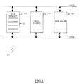
- the memory system 100 includes a data processor, e.g. microprocessor 105, a main memory device 110 and a cache memory system 115, responsible of managing the exchange of data from the main memory device 110 to the microprocessor 105 and vice versa.
- the main memory device 110 includes a plurality of main memory storage locations 112, that can be read or written by the microprocessor 105.
- signals and corresponding physical lines carrying them are denoted with the same references.
- the memory system 100 further includes an address bus ADDR and a data bus DATA, connecting the microprocessor 105, the main memory device 110 and the cache memory system one to each others, allowing the exchange of data and, respectively, addresses.
- the ensemble of all possible addresses ADDR defines the address space of the main memory, in the sense that each main memory location 112 corresponds to a particular address ADDR. It is important to underline that in the following description "main memory cache lines” and “main memory locations” are considered synonyms, for the sake of the description simplicity (as mentioned in the foregoing, a main memory cache line may in the practice correspond to two or more main memory locations).
- the cache memory system 115 includes a RAM device 205 that, according to the present invention, is used as a unified tag cache and data cache memory, and is adapted to store both data and tags.
- the RAM device 205 may be a static RAM, having address terminals for receiving a cache address CADDR, data output terminals for providing data OUT read out from the RAM device 205 (data and/or tags), data input terminals for receiving data DIN from the main memory device 110, and a write enable terminal which receives, from a controller block 210 controlling the cache memory system, a write enable signal WEN for enabling writing operations.
- the RAM device 205 includes a two dimensional memory array 215 having a plurality of addressable RAM locations RLj adapted to store tag words TAG1, TAG2, ..., TAGi, and corresponding cache lines DATA1, DATA2, ..., DATAi.
- the ensemble of all possible cache addresses CADDR defines the address space of the cache memory, in the sense that each RAM location RLj corresponds to a particular cache address CADDR.
- each cache line DATAi has (in the example herein considered) a bit width equal to the bit width of a main memory location 112; thus, the generic cache line represents the data contained in a corresponding, cached main memory location.
- a tag word TAGi and/or a cache line DATAi can be split so as to be stored into two or more different, preferably but non necessarily, consecutive, RAM locations RLj; the generic tag word TAGi, and/or the generic cache line DATAi are divided into two or more chunks, each chunk being stored in a different RAM location RLj. Thanks to this particular arrangement, it is possible to efficiently use the storage capacity of the RAM device 205: in particular, the RAM locations RLj can be completely filled by tag and/or data irrespectively of the dimensions of tag words TAGi and cache lines DATAi, without wasting memory space.
- the cache memory system 115 receives an address ADDR (corresponding to a main memory location 112) that is provided to a tag mapping function block Ft and to a data mapping function block Fd. Said address ADDR is used by the tag mapping function block Ft and the data mapping function block Fd for the identification of a tag word TAGi and of a corresponding cache line DATAi in the RAM device 205.
- the tag mapping function block Ft is a logic block adapted to process the received address ADDR for generating a tag address ADDRtag; the tag address ADDRtag is used to generate a corresponding cache address CADDR, and a tag offset value OFFSETtag.
- the data mapping function block Fd is a logic block adapted to process the received address ADDR for generating a data address ADDRdata; the data address ADDRdata is used to generate a corresponding cache address CADDR, and a data offset value OFFSETdata. More particularly, the tag address ADDRtag, together with the tag offset value OFFSETtag, allows to identify the position of a tag word TAGi within the RAM device 205, while the data address ADDRdata, together with the data offset value OFFSETdata, allows to identify the position of a cache line DATAi within the RAM device 205.
- the tag mapping function block Ft and the data mapping function block Fd (with the help of other circuital blocks that will be presented hereinafter) establish an injective correspondence between the conventional address space of the main memory and the address space of the cache memory according to a particular mapping.
- the tag address ADDRtag and the data address ADDRdata are provided to two input terminals of a multiplexer 220, receiving, at its control terminal, an address control signal ACTR from the controller block 210.
- the output terminal of the multiplexer 220 is connected to the input terminal of an address value incrementer/decrementer 225, that generates and provides the cache address CADDR to the RAM device 205 as a function of an up/down control signal provided by the controller block 210.
- the address value incrementer/decrementer 225 is adapted to increment/decrement the address received from the multiplexer 220 (i.e., either the tag address ADDRtag or the data address ADDRdata) in case the addressed tag word TAGi or the addressed cache line DATAi are spread over two or more RAM locations RLj, possibly consecutive, which correspond to two or more, possibly consecutive cache addresses CADDR.
- a tag word TAGi is assumed to be spread over two consecutive RAM locations RL(j-1) and RLj. These two RAM locations correspond to two consecutive cache address CADDR, equal to (ADDRtag)a (address of the RAM location RL(j-1) including the first chunk of the tag word TAGi) and (ADDRtag)a+1 (address of the RAM location RL(j) including the second chunk of the tag word TAGi), respectively.
- the first chunk of the tag word TAGi does not occupy entirely the RAM location RL(j-1), and is instead shifted with respect to the first bit of the RAM location RL(j-1) by an amount of bits which depends on the tag offset value (OFFSETtag)a. Similar considerations apply in respect of the data address ADDRdata and the data offset value OFFSETdata.
- the tag offset value OFFSETtag is provided to a first input terminal of an adder block 226, which receives at a second input terminal a control tag value CT provided by the controller block 210.
- the control tag value CT is added to the tag offset value OFFSETtag in order to generate an alignment offset tag value AOt necessary for aligning output words provided by the RAM device 205 in a tag retrieval operation, as will be explained in the following.
- the data offset value OFFSETdata is provided to a first input terminal of an adder block 228, which receives at a second input terminal a control data value CD provided by the controller block 210.
- the control data value CD is added to the data offset value OFFSETdata in order to generate an alignment offset data value AOd.
- the RAM device 205 When accessed in reading, the RAM device 205 provides at its output terminal an output word OUT; the output word OUT may be the contents of a RAM location RLj including a chunk of a tag word TAGi, or a chunk of a cache line DATAi, depending on the operations that the cache memory system 115 is executing. Said output word OUT is supplied to respective first input terminals of two shifters 230 and 235.
- the shifter 230 has a second input terminal receiving the alignment offset data value AOd
- the shifter 235 has a second input terminal receiving the aligned offset tag value AOt.
- the operations of the shifters 230 and 235 are synchronized by a clock signal CK (i.e., the clock signal of the memory) provided by the controller block 210.
- the shifter 235 includes a register adapted to execute shifting operations that are necessary to align the output data words OUT read from the RAM device 205 (in this case, including chunks of tag words TAGi) in such a way that it is possible to reconstruct an entire tag word TAGi by output data words OUT obtained by reading in succession two or more, possibly, consecutive locations of the RAM device 205.
- the shifter 235 has a bit width WBS that is equal to the bit width WT of the tag word TAGi, that, in the example herein considered, is greater than the bit width WRL of the RAM location RLj.
- the shifter 235 is connected to a tag register 238, having a bit width equal to the bit width WT of the tag word TAGi.
- the tag register 238 is controlled by the controller block 210 by means of a tag enable bus Et, having a number of lines equal to the number of bits that the tag register 238 can store.
- the shifter 235 is capable to align a received output data word OUT, using the alignment offset tag value AOt.
- the shifter 235 firstly stores the first output data word OUT, then aligns it using the alignment offset tag value AOt in such a way to eliminate the offset given by the tag offset value (OFFSETtag)a, and provides the bits of the aligned first chunk of the word tag TAGi to the tag register 238 in the correct positions, using an indication given by the controller block 210 by means of the tag enable bus Et.
- the shifter 235 stores the second output word OUT, and aligns it in such a way to provide the bits of the second chunk of the tag word TAGi to the tag register 238 adjacently to the ones of the first chunk of the tag word TAGi previously stored, so as to reconstruct the complete tag word TAGi.
- Similar considerations apply for the shifter 230, adapted to store and execute shifting operations to reconstruct cache lines DATAi.
- the shifter 230 is connected to a data register 240, having a bit width adapted to store a cache line DATAi.
- the tag word TAGi is transferred from the tag register to a first input of a comparator block 245.
- the comparator block 245 includes a second input receiving a tag portion TAGp of the address ADDR.
- the comparator block 245 further includes an output terminal for providing an hit/miss signal, indicating if a cache hit or a cache miss is occurred.
- Input data DIN to be written into the RAM device 205 are received by means of the address bus ADDR (for tag words replacements) and the data bus DATA (for cache lines replacements); the data may be received from the microprocessor 105 or the main memory 110.
- a multiplexer block 250 has a first input connected to the address bus ADDR, a second input connected to the data bus DATA, a control terminal receiving a selection signal SEL from the controller block 210, and an output connected to an input of a mask block 252.
- the selection signal SEL is asserted by the controller block 210 in such a way to select the data bus DATA: in this way, the input data DIN to be written into the RAM device 205 are derived from the data bus DATA; otherwise, when a tag word TAGi has to be written (which typically occurs in case of a cache miss, when a new main memory cache line has to be cached), the selection signal SEL is asserted in such a way to select the address bus ADDR: in this way, the input data DIN to be written into the RAM device 205 are derived from the address bus ADDR.
- the mask block receives a mask control signal MSK from the controller block 210, the alignment offset tag value AOt from the adder block 226, and the alignment offset data value AOD from the adder block 228.
- the mask block 252 is adapted to receive a word (TAGi or DATAi) provided by the multiplexer block 250, and to perform consequently a plurality of operations (including word truncations and alignments), necessary to generate input data DIN (including chunks of tag word TAGi or cache line DATAi) that are to be stored in the RAM locations RLj.
- the mask block 252 is adapted to receive also output data words OUT. For example, having to store the tag word TAG1 received entirely (in a single time) by means of the address bus ADDR into two RAM locations, in the manner shown in Figure 2, the mask block 252 provides for dividing the tag word TAG1 in two chunks, shifting them by means of the alignment offset tag value AOt and the alignment offset data value AOD, preparing two words having bit widths equal to the bit width WRL of the RAM location, and "masking" the bits that are not to be overwritten in said two RAM locations (e.g., having the first chunk of the tag word TAG1 a bit width smaller than the bit width WRL, a group of bits - in this case the first bits - must remain unchanged).
- the microprocessor 105 when the microprocessor 105 requests the reading of the content of a main memory location 112 corresponding to an address ADDR, it provides this address to the cache memory system 115, that in response retrieves a corresponding tag word TAGi from the RAM device 205.
- the search of said tag word TAGi is performed by means of the circuital blocks Ft, 225, 210, 235, 238 and 245, described previously. If the retrieved tag word TAGi results equal to the tag portion TAGp of the current address ADDR (cache hit), it means that the content of the addressed main memory location 112 is cached in a cache line DATAi stored in the RAM device 205.
- the cache memory system then retrieves the desired cache line DATAi, possibly by performing one or more additional read accesses to the memory 205, so as to place the cache line DATAi into the data register 240; the cache line DATAi is then provided to the microprocessor 105.
- the method illustrated may involve more than one consecutive accesses to the RAM device 205.
- the generic tag word TAGi and/or the generic cache line DATAi may be divided in chunks, which are stored into different RAM locations RLj.
- the data stored in the main memory cache line including the addressed main memory location 112 are cached, and the tag portion TAGp of the address ADDR is stored in the RAM device 205 (in particular, the data become a cache line DATAi, and the tag portion TAGp of the address ADDR becomes a corresponding tag word TAGi). Also in this case, more than one access to the RAM device 205 may in general be required.
- An important feature of the cache system according to the described embodiment of the present invention consists in the possibility to efficiently fill the memory array 215 of the RAM device 205, minimizing the number of unused RAM locations RLj or portions thereof This can be achieved thanks to the great flexibility allowed by the proposed method of filling in the locations in the memory array 215 of the RAM device 205 with tag words and cache lines. In this way, it is possible to reduce the size of the RAM device, and to reduce the number of required RAM devices 205, thus saving silicon area and reducing power consumptions.
- Another advantage of said filling flexibility consists in the fact that it is not necessary to design a dedicated RAM device 205 having the exact capacity and the exact dimensions (number of locations and bit width) necessary for storing the desired tag words, and the corresponding cache lines in a same, unique RAM location.
- a cache memory system is to be designed including 8192 cache lines DATAi having a bit width WD which value is equal to 32, and having a "block size" equal to 2 (i.e., at each tag corresponds two cache lines). Consequently, 4096 (4K) tag words TAGi will be necessary. Moreover, according to this example each tag word TAGi has a bit width WT whose value is equal to 20.
- a single RAM device 205 is used for storing both the tag words and the cache lines; in particular, the RAM device may include a 8K*42 memory array 215 (i.e., an array with 8192 RAM locations RLj having a bit width WRL whose value is equal to 42, as illustrated in Figure 5).
- the RAM device is fully used, without any waste of memory space.
- mapping functions performed by the tag mapping function block Ft and the data mapping function block Fd allows to arrange all the TAG words in a first portion of the array 215, adjacent one to the other, and all the cache lines DATAi are similarly arranged in a second portion of the array 215, as well adjacent one to another.
- the TAG words are for example stored in the RAM locations RLj with lowest addresses, starting from the lowest-addresses location; the cache lines DATAi are arranged consecutively and adjacently in the RAM locations RLj with highest addresses, starting from the last location of the array portion dedicated to the tag words.
- ADDR a ⁇ 20 / 42 wherein "20” is the value of the bit width WT of the generic tag word TAGi, and "42" is the value of the bit width WRL of the RAM locations RLi.
- an N-way set-associative cache can be for example realized by using N RAM devices 205, arranged similarly, one RAM devices per way.
- a cache memory system is to be designed including 8192 caches lines DATAi having a bit width WD whose value is equal to 16.
- the cache system is assumed to have a block size equal to 1. Consequently, 8192 (8K) tag words TAGi will be necessary.
- each tag word TAGi has a bit width WT whose value is equal to 20.
- a cache memory system may be realized using a single RAM device 205 for storing tag words and cache lines having a 16K*18 memory array 215 (i.e., with 16384 RAM locations RLj having a bit width WRL which value is equal to 18, as illustrated in Figure 6) per each way.
- the number of ways is equal to two. Each way corresponds to a RAM device 205.
- Each RAM location RLj belonging to the cache zone LANE0 is paired with a corresponding RAM location RL(j+8192) belonging to the cache zone LANE1 (e.g., their cache addresses CADDR differ in the most significant bit).
- Each RAM location RLj belonging to the cache zone LANE0 stores a chunk of tag word TAGi, corresponding to the 18 least significant bits thereof.
- the corresponding RAM location RL(j+8192) belonging to the cache zone LANE1 includes the second chunk of the tag word TAGi comprising the remaining two, most significant bits, while the residual 16 bits store a corresponding cache line DATAi. According to this particular mapping, it is possible to speed up the operations performed by the cache memory system 115; particularly, a cache miss can be decreed in a reduced time.
- the tag comparison operation executed by the comparator block 245 is first executed on the 18 least significant bits of the tag word TAGi chunk retrieved by performing a first access to the RAM device 205. If said 18 least significant bits of the tag word TAGi result different from the 18 least significant bits of the tag portion TAGp of the address ADDR, a cache miss is decreed, without the need of retrieving the remaining chunk of the TAG word; otherwise, the cache memory system 115 operates a second access on the corresponding RAM location in the cache zone LANE1 (simply inverting the most significant bit of the cache addresses), for obtaining the remaining two bits of the second chunk of the tag word TAGi.
- the comparator block 245 compares said second chunk with the two most significant bits of the tag portion TAGp of the address ADDR.
- the corresponding cache line DATAi already read out from the memory, is exploited. Thanks to this particular access policy, the switching activity of the address lines of the RAM memory device 205 is reduced, implying a reduced power consumption; in fact, the cache addresses CADDR of RAM locations corresponding to the two different cache zones LANEO, LANE1 and storing chunks of the same tag word TAGi differs only by the most significant bit.
- a two-way cache memory system 700 having a block size equal to 2 may be conveniently implemented storing the tag words of the two ways (TAG WAY 0, TAG WAY 1) together with the cache lines of a way (DATA WAY 0) in a single memory device 710, without wasting memory space.
- the cache lines of the other way (DATA WAY 0) may be stored in a further memory device 720.
- an advantageous cache mapping architecture may be obtained storing into a single memory device the tag words of all the ways together with the cache lines of a way.
- the concepts of the present invention remain applicable in case some or all the operations performed by the functional blocks hereinabove described are performed by means of software/firmware tools, e.g., if part or all of said functional blocks (like for example the address value incrementer/decrementer 225, the shifters 230, 235, and so on) are implemented in terms of instructions executed by a suitable-programmed, e.g. embedded micro controller.
Abstract
Description
- The present invention relates to the memory field. More particularly, the present invention relates to cache memory systems.
- Data processors like microprocessors used in personal computers rely for the execution of the intended programs on working memories ("main memories") typically constituted by banks of Dynamic RAMs (DRAMs).
- Modem data processors however operates at speeds which exceed the usual DRAMs access times. To overcome such problems, and allow the processor to run near its clock speed, cache memory systems including cache memories are used.
- A cache memory (hereinafter also referred to as "cache", for brevity) is a relatively small, but fast memory (typically, a Static RAM - SRAM), which stores (or "caches") copies of the data content of the most frequently, or more recently accessed main memory locations. As long as most memory accesses are made to cached main memory locations, instead of to the main memory itself, the average latency of memory accesses is closer to the cache latency than to the latency of the main memory.
- A typical cache memory system comprises two different memory components. A first memory component, referred to as "data cache", which is usually the larger of the two, is a memory which stores the copies of the data or the instructions needed by the processor, so that such information need not be retrieved from the main memory. A second memory component, referred to as the "tag cache", is used to store portions of main memory addresses. The data cache includes a plurality of storage locations, called "cache lines"; usually, the width (in terms of number of bits) of the generic cache line is larger than the width of the generic main memory location; thus, when a generic main memory location is accessed, a corresponding group of main memory locations is actually cached into the cache memory; the terms cache lines is also used to identify one of said groups of main memory locations. Each cache line of the data cache is associated with a corresponding location in the tag cache, which contains a "tag"; the tag represent a portion of a main memory address, identifying a respective cache line in the main memory which has been cached into that cache line of the data cache.
- When the processor has to read or write a main memory location, it issues a main memory address code, which identifies a cache line in the main memory; the cache memory system checks whether the addressed cache line is present in the cache. This is accomplished by comparing the part of the main memory address code identifying the addressed cache line (i.e., the tag portion of the address) to all the tags stored in the tag cache locations. If it is found that the addressed main memory cache line is in the cache, a cache "hit" is decreed, otherwise the cache memory system decrees a cache "miss". In the case of a cache hit, the processor immediately reads/writes the data from/into the proper cache line of the data cache, otherwise the main memory is accessed. In case of a cache miss, the operations take more time, because they require the data transfer from the main memory, which is much slower than the cache memory. The higher the number of cache hits (known as the "hit rate"), the more effective is the cache.
- In the case of a cache miss, most caches allocate a new entry, which comprises the tag just missed and a copy of the corresponding data from the main memory. If the cache is already full, one of the existing cache entries in the data cache (and the corresponding entry in the tag cache) needs to be removed. The modality that it is used to choose the cache line to be replaced is called the "replacement policy". As known in the art, one popular replacement policy (Least Recently Used, LRU) replaces the least recently used entry.
- When the data stored in a cache line of the cache memory are changed in consequence of a write access requested by the processor, the data stored in the main memory need to be updated. The moment in time when the updating operation is performed depends on the so-called "write policy" of the memory system. A known write policy, called "write-through", provides that every write to the cache causes an immediate write to the main memory. Alternatively, according to the so-called "write-back" policy, writes to the cache are not immediately performed as well onto the memory: the cache keeps track of which cache lines have been modified, and the data in these cache lines are written back to the main memory when that cache line has to be used for caching a different main memory cache line. For this reason, a miss in a write-back cache will often require two memory accesses to service.
- A very important factor in determining the effectiveness of a cache relates to how the cache is mapped onto the main memory. Three different approaches to allocate the data in the cache according to the corresponding main memory addresses are known in the art.
- The simplest approach to map the cache onto the main memory, called "direct mapping", calls for determining how many cache lines there are in the data cache memory, and divide the main memory into the same number of cache lines. Therefore, when a generic one of said main memory cache lines is cached, it fills a predetermined one of said data cache lines.
- Instead of establishing a rigid correspondence between cache lines of the data cache memory and main memory cache lines, it is possible to design the cache so that any cache line can store the data contents of any main memory cache line. This approach is called "fully associative mapping".
- A compromise between the direct mapping and the fully associative mapping is the so-called "N-way set associative mapping". In this case, the cache is divided into sets, each set containing a number N of cache lines (each one corresponding to a "way"). Typically, N may be equal to 2, 4 or 8. The main memory address space is divided into corresponding sets, and the generic main memory cache line can be cached into any one of the N cache lines of the corresponding set (determined on the basis of the main memory address). In other words, within each cache line set the cache is associative.
- Cache memory systems may be embedded in, e.g., microprocessor integrated circuits (so-called embedded processor ICs).
- The power consumption of a cache memory systems represents an important fraction of the overall power consumption of an embedded processor IC. Nowadays, cache memory systems are implemented providing within an IC chip different static RAM devices (SRAMs), corresponding to the tag cache and the data cache for each way. This solution, although improving hit rate and memory access times performances, needs the replication of all the circuits necessary for the functioning of the memory (input/output buffers, decoders, read circuits, write circuits and so on) per each SRAMs, thus involving a higher waste of semiconductor area and higher power consumption. Moreover, the RAM memories specifically designed for high-performance cache memory systems (adapted to access data and tags in a same clock cycle) exhibit an elevated static power dissipation.
- In view of the state of the art outlined in the foregoing, the Applicant has faced the general problem of how to implement a cache memory system in an efficient way, assuring low power consumptions.
- According to the present invention, a cache memory system as set forth in
claim 1 is provided. - The cache memory system comprises at least one cache memory and a cache memory controller; the at least one cache memory includes a plurality of storage locations, each one identified by a corresponding cache address and adapted to store tag address portions and data words, each data word corresponding to a respective tag address portion; the cache memory controller is adapted to receive a first address and to access the at least one cache memory based on the received first address. The cache memory controller includes a first address transformer adapted to receive the first address and to transform it into at least one first cache address corresponding thereto by applying a first transform function, the at least one first cache address being used by the cache memory controller for accessing the at least one cache memory to retrieve at least a first part of a tag address portion stored in at least one of the storage locations. The cache memory controller further includes a hit detector adapted to establish an at least partial hit condition based on a comparison of the retrieved at least a first part of the tag address portion and a first predetermined part of the first address, and a second address transformer adapted to receive the first address and to transform it into at least one second cache address corresponding thereto by applying a second transform function; the cache memory controller is adapted to use the at least one second cache address for accessing the at least one cache memory to retrieve a data word corresponding to the retrieved tag address portion in case said at least partial hit condition is established.
- In this way, the cache memory system implements an asymmetric logic mapping of tag address portions and data words in the memory.
- Further features and advantages of the present invention will be made clear by the following detailed description of a preferred embodiment thereof, provided purely by way of a non-limitative example, with reference to the attached drawings, wherein:
- Figure 1 schematically shows a functional block diagram of a memory system, according to an embodiment of the present invention;
- Figure 2 schematically illustrates a functional block diagram of an exemplary cache memory system, according to an embodiment of the present invention;
- Figure 3 illustrates an exemplary use of a single RAM memory device for storing data and tags, according to an embodiment of the present invention;
- Figure 4 schematically shows a block diagram of a shifter included in the cache memory system , according to an embodiment of the present invention;
- Figure 5 illustrates an exemplary tags and cache lines mapping on the RAM memory device according to an embodiment of the present invention;
- Figure 6 illustrates another tags and cache lines mapping on two RAM memory devices according to another embodiment of the present invention;
- Figure 7 illustrates an exemplary tags and cache lines mapping on two RAM memory devices, according to a still another embodiment of the present invention.
- More particularly, referring to Figure 1, an exemplary and schematic functional block diagram of a
memory system 100 is illustrated. More particularly, thememory system 100 includes a data processor,e.g. microprocessor 105, amain memory device 110 and acache memory system 115, responsible of managing the exchange of data from themain memory device 110 to themicroprocessor 105 and vice versa. Themain memory device 110 includes a plurality of mainmemory storage locations 112, that can be read or written by themicroprocessor 105. In this Figure, and in the following ones, for the sake of simplicity, signals and corresponding physical lines carrying them are denoted with the same references. Thememory system 100 further includes an address bus ADDR and a data bus DATA, connecting themicroprocessor 105, themain memory device 110 and the cache memory system one to each others, allowing the exchange of data and, respectively, addresses. The ensemble of all possible addresses ADDR defines the address space of the main memory, in the sense that eachmain memory location 112 corresponds to a particular address ADDR. It is important to underline that in the following description "main memory cache lines" and "main memory locations" are considered synonyms, for the sake of the description simplicity (as mentioned in the foregoing, a main memory cache line may in the practice correspond to two or more main memory locations). - Referring to Figure 2, a more detailed functional block diagram of an exemplary
cache memory system 115 is illustrated, according to an embodiment of the present invention. Thecache memory system 115 includes aRAM device 205 that, according to the present invention, is used as a unified tag cache and data cache memory, and is adapted to store both data and tags. TheRAM device 205 may be a static RAM, having address terminals for receiving a cache address CADDR, data output terminals for providing data OUT read out from the RAM device 205 (data and/or tags), data input terminals for receiving data DIN from themain memory device 110, and a write enable terminal which receives, from acontroller block 210 controlling the cache memory system, a write enable signal WEN for enabling writing operations. TheRAM device 205 includes a twodimensional memory array 215 having a plurality of addressable RAM locations RLj adapted to store tag words TAG1, TAG2, ..., TAGi, and corresponding cache lines DATA1, DATA2, ..., DATAi. The ensemble of all possible cache addresses CADDR defines the address space of the cache memory, in the sense that each RAM location RLj corresponds to a particular cache address CADDR. Moreover, each cache line DATAi has (in the example herein considered) a bit width equal to the bit width of amain memory location 112; thus, the generic cache line represents the data contained in a corresponding, cached main memory location. As it can be seen in Figure 2, a tag word TAGi and/or a cache line DATAi can be split so as to be stored into two or more different, preferably but non necessarily, consecutive, RAM locations RLj; the generic tag word TAGi, and/or the generic cache line DATAi are divided into two or more chunks, each chunk being stored in a different RAM location RLj. Thanks to this particular arrangement, it is possible to efficiently use the storage capacity of the RAM device 205: in particular, the RAM locations RLj can be completely filled by tag and/or data irrespectively of the dimensions of tag words TAGi and cache lines DATAi, without wasting memory space. - The
cache memory system 115 receives an address ADDR (corresponding to a main memory location 112) that is provided to a tag mapping function block Ft and to a data mapping function block Fd. Said address ADDR is used by the tag mapping function block Ft and the data mapping function block Fd for the identification of a tag word TAGi and of a corresponding cache line DATAi in theRAM device 205. The tag mapping function block Ft is a logic block adapted to process the received address ADDR for generating a tag address ADDRtag; the tag address ADDRtag is used to generate a corresponding cache address CADDR, and a tag offset value OFFSETtag. Similarly, the data mapping function block Fd is a logic block adapted to process the received address ADDR for generating a data address ADDRdata; the data address ADDRdata is used to generate a corresponding cache address CADDR, and a data offset value OFFSETdata. More particularly, the tag address ADDRtag, together with the tag offset value OFFSETtag, allows to identify the position of a tag word TAGi within theRAM device 205, while the data address ADDRdata, together with the data offset value OFFSETdata, allows to identify the position of a cache line DATAi within theRAM device 205. In other words, the tag mapping function block Ft and the data mapping function block Fd (with the help of other circuital blocks that will be presented hereinafter) establish an injective correspondence between the conventional address space of the main memory and the address space of the cache memory according to a particular mapping. - The tag address ADDRtag and the data address ADDRdata are provided to two input terminals of a
multiplexer 220, receiving, at its control terminal, an address control signal ACTR from thecontroller block 210. The output terminal of themultiplexer 220 is connected to the input terminal of an address value incrementer/decrementer 225, that generates and provides the cache address CADDR to theRAM device 205 as a function of an up/down control signal provided by thecontroller block 210. The address value incrementer/decrementer 225 is adapted to increment/decrement the address received from the multiplexer 220 (i.e., either the tag address ADDRtag or the data address ADDRdata) in case the addressed tag word TAGi or the addressed cache line DATAi are spread over two or more RAM locations RLj, possibly consecutive, which correspond to two or more, possibly consecutive cache addresses CADDR. - Referring to Figure 3, an exemplary use of a tag address ADDRtag and a tag offset value OFFSETtag is illustrated. Assuming that WRL denotes a bit width of the generic RAM location RLj, and that WT denotes a bit width of the generic tag word TAGi, a tag word TAGi is assumed to be spread over two consecutive RAM locations RL(j-1) and RLj. These two RAM locations correspond to two consecutive cache address CADDR, equal to (ADDRtag)a (address of the RAM location RL(j-1) including the first chunk of the tag word TAGi) and (ADDRtag)a+1 (address of the RAM location RL(j) including the second chunk of the tag word TAGi), respectively. Referring again to the example illustrated in Figure 3, the first chunk of the tag word TAGi does not occupy entirely the RAM location RL(j-1), and is instead shifted with respect to the first bit of the RAM location RL(j-1) by an amount of bits which depends on the tag offset value (OFFSETtag)a. Similar considerations apply in respect of the data address ADDRdata and the data offset value OFFSETdata.
- Referring back to Figure 2, the tag offset value OFFSETtag is provided to a first input terminal of an
adder block 226, which receives at a second input terminal a control tag value CT provided by thecontroller block 210. The control tag value CT is added to the tag offset value OFFSETtag in order to generate an alignment offset tag value AOt necessary for aligning output words provided by theRAM device 205 in a tag retrieval operation, as will be explained in the following. Similarly, the data offset value OFFSETdata is provided to a first input terminal of anadder block 228, which receives at a second input terminal a control data value CD provided by thecontroller block 210. The control data value CD is added to the data offset value OFFSETdata in order to generate an alignment offset data value AOd. - When accessed in reading, the
RAM device 205 provides at its output terminal an output word OUT; the output word OUT may be the contents of a RAM location RLj including a chunk of a tag word TAGi, or a chunk of a cache line DATAi, depending on the operations that thecache memory system 115 is executing. Said output word OUT is supplied to respective first input terminals of twoshifters shifter 230 has a second input terminal receiving the alignment offset data value AOd, and theshifter 235 has a second input terminal receiving the aligned offset tag value AOt. Moreover, the operations of theshifters controller block 210. - Referring now to Figure 4, a more detailed view of an exemplary shifter (e.g., the shifter 235) is illustrated. The
shifter 235 includes a register adapted to execute shifting operations that are necessary to align the output data words OUT read from the RAM device 205 (in this case, including chunks of tag words TAGi) in such a way that it is possible to reconstruct an entire tag word TAGi by output data words OUT obtained by reading in succession two or more, possibly, consecutive locations of theRAM device 205. Theshifter 235 has a bit width WBS that is equal to the bit width WT of the tag word TAGi, that, in the example herein considered, is greater than the bit width WRL of the RAM location RLj. Moreover, theshifter 235 is connected to atag register 238, having a bit width equal to the bit width WT of the tag word TAGi. Moreover, thetag register 238 is controlled by thecontroller block 210 by means of a tag enable bus Et, having a number of lines equal to the number of bits that thetag register 238 can store. Theshifter 235 is capable to align a received output data word OUT, using the alignment offset tag value AOt. For example, if a tag word TAGi is stored in two consecutive RAM locations RL(j-1), RLj, theshifter 235 firstly stores the first output data word OUT, then aligns it using the alignment offset tag value AOt in such a way to eliminate the offset given by the tag offset value (OFFSETtag)a, and provides the bits of the aligned first chunk of the word tag TAGi to thetag register 238 in the correct positions, using an indication given by thecontroller block 210 by means of the tag enable bus Et. Successively, theshifter 235 stores the second output word OUT, and aligns it in such a way to provide the bits of the second chunk of the tag word TAGi to thetag register 238 adjacently to the ones of the first chunk of the tag word TAGi previously stored, so as to reconstruct the complete tag word TAGi. Similar considerations apply for theshifter 230, adapted to store and execute shifting operations to reconstruct cache lines DATAi. In this case, theshifter 230 is connected to adata register 240, having a bit width adapted to store a cache line DATAi. When the tag word TAGi has been stored and reconstructed, the tag word TAGi is transferred from the tag register to a first input of acomparator block 245. Thecomparator block 245 includes a second input receiving a tag portion TAGp of the address ADDR. Thecomparator block 245 further includes an output terminal for providing an hit/miss signal, indicating if a cache hit or a cache miss is occurred. - Input data DIN to be written into the
RAM device 205 are received by means of the address bus ADDR (for tag words replacements) and the data bus DATA (for cache lines replacements); the data may be received from themicroprocessor 105 or themain memory 110. In particular, amultiplexer block 250 has a first input connected to the address bus ADDR, a second input connected to the data bus DATA, a control terminal receiving a selection signal SEL from thecontroller block 210, and an output connected to an input of amask block 252. When a cache line DATAi has to be written into theRAM device 205, for example in the case of a cache miss (a new main memory cache line has to be cached), or, in the case of a cache hit, should the microprocessor perform a write operation, the selection signal SEL is asserted by thecontroller block 210 in such a way to select the data bus DATA: in this way, the input data DIN to be written into theRAM device 205 are derived from the data bus DATA; otherwise, when a tag word TAGi has to be written (which typically occurs in case of a cache miss, when a new main memory cache line has to be cached), the selection signal SEL is asserted in such a way to select the address bus ADDR: in this way, the input data DIN to be written into theRAM device 205 are derived from the address bus ADDR. These writing operations are executed with the aid of themask block 252 and of the previously described circuitry for the generation of the cache address CADR (for selecting the locations of theRAM device 205 to be written). The mask block receives a mask control signal MSK from thecontroller block 210, the alignment offset tag value AOt from theadder block 226, and the alignment offset data value AOD from theadder block 228. Moreover, themask block 252 is adapted to receive a word (TAGi or DATAi) provided by themultiplexer block 250, and to perform consequently a plurality of operations (including word truncations and alignments), necessary to generate input data DIN (including chunks of tag word TAGi or cache line DATAi) that are to be stored in the RAM locations RLj. These operations require preliminary reading of the contents of the RAM locations RLj, because the word alignments may imply that some bits previously stored have to be protected against overwriting. Consequently, themask block 252 is adapted to receive also output data words OUT. For example, having to store the tag word TAG1 received entirely (in a single time) by means of the address bus ADDR into two RAM locations, in the manner shown in Figure 2, themask block 252 provides for dividing the tag word TAG1 in two chunks, shifting them by means of the alignment offset tag value AOt and the alignment offset data value AOD, preparing two words having bit widths equal to the bit width WRL of the RAM location, and "masking" the bits that are not to be overwritten in said two RAM locations (e.g., having the first chunk of the tag word TAG1 a bit width smaller than the bit width WRL, a group of bits - in this case the first bits - must remain unchanged). - Briefly reassuming the operations performed by the
cache memory system 115, when themicroprocessor 105 requests the reading of the content of amain memory location 112 corresponding to an address ADDR, it provides this address to thecache memory system 115, that in response retrieves a corresponding tag word TAGi from theRAM device 205. The search of said tag word TAGi is performed by means of the circuital blocks Ft, 225, 210, 235, 238 and 245, described previously. If the retrieved tag word TAGi results equal to the tag portion TAGp of the current address ADDR (cache hit), it means that the content of the addressedmain memory location 112 is cached in a cache line DATAi stored in theRAM device 205. The cache memory system then retrieves the desired cache line DATAi, possibly by performing one or more additional read accesses to thememory 205, so as to place the cache line DATAi into the data register 240; the cache line DATAi is then provided to themicroprocessor 105. As mentioned, the method illustrated may involve more than one consecutive accesses to theRAM device 205. In fact, for the efficient exploitation of the storage capability of theRAM device 205, the generic tag word TAGi and/or the generic cache line DATAi may be divided in chunks, which are stored into different RAM locations RLj. In the case of a cache miss (retrieved tag word TAGi different from the tag portion TAGp), the data stored in the main memory cache line including the addressedmain memory location 112 are cached, and the tag portion TAGp of the address ADDR is stored in the RAM device 205 (in particular, the data become a cache line DATAi, and the tag portion TAGp of the address ADDR becomes a corresponding tag word TAGi). Also in this case, more than one access to theRAM device 205 may in general be required. - An important feature of the cache system according to the described embodiment of the present invention consists in the possibility to efficiently fill the
memory array 215 of theRAM device 205, minimizing the number of unused RAM locations RLj or portions thereof This can be achieved thanks to the great flexibility allowed by the proposed method of filling in the locations in thememory array 215 of theRAM device 205 with tag words and cache lines. In this way, it is possible to reduce the size of the RAM device, and to reduce the number of requiredRAM devices 205, thus saving silicon area and reducing power consumptions. Another advantage of said filling flexibility consists in the fact that it is not necessary to design adedicated RAM device 205 having the exact capacity and the exact dimensions (number of locations and bit width) necessary for storing the desired tag words, and the corresponding cache lines in a same, unique RAM location. - Hereinafter, two different examples of implementation for the mapping of tag words TAGi and cache lines DATAi will be illustrated.
- According to a first example, it is assumed that a cache memory system is to be designed including 8192 cache lines DATAi having a bit width WD which value is equal to 32, and having a "block size" equal to 2 (i.e., at each tag corresponds two cache lines). Consequently, 4096 (4K) tag words TAGi will be necessary. Moreover, according to this example each tag word TAGi has a bit width WT whose value is equal to 20. In this case, according to an embodiment of the present invention, a
single RAM device 205 is used for storing both the tag words and the cache lines; in particular, the RAM device may include a 8K*42 memory array 215 (i.e., an array with 8192 RAM locations RLj having a bit width WRL whose value is equal to 42, as illustrated in Figure 5). In this way, the RAM device is fully used, without any waste of memory space. In fact:
- A possible implementation of the mapping functions performed by the tag mapping function block Ft and the data mapping function block Fd allows to arrange all the TAG words in a first portion of the
array 215, adjacent one to the other, and all the cache lines DATAi are similarly arranged in a second portion of thearray 215, as well adjacent one to another. In particular, the TAG words are for example stored in the RAM locations RLj with lowest addresses, starting from the lowest-addresses location; the cache lines DATAi are arranged consecutively and adjacently in the RAM locations RLj with highest addresses, starting from the last location of the array portion dedicated to the tag words. More particularly, the generation of the tag address ADDRtag and of the tag offset value OFFSETtag starting from the address ADDR is accomplished by the tag mapping function block Ft in the following way:

wherein "20" is the value of the bit width WT of the generic tag word TAGi, and "42" is the value of the bit width WRL of the RAM locations RLi. - The generation of the data address ADDRdata and of the data offset value OFFSETdata starting from the address ADDR is similarly accomplished by the tag mapping function block Fd:


wherein "database" is a value that corresponds to the cache address CADDR of to the last RAM locations RLj in the array portion dedicated to the tag words, in the example considered equal to "int(4096*20/42)"; "baseoffset" represents the data offset value (OFFSETdata)a of the first cache line (i.e., the one adjacent to the last tag word) within the last RAM location storing a TAG word; in the considered example, baseoffset is equal to "mod(42,(4095*20/42))+1". - The example just described relates to a 1-way set-associative cache; an N-way set-associative cache can be for example realized by using
N RAM devices 205, arranged similarly, one RAM devices per way. - According to a second example, it is assumed that a cache memory system is to be designed including 8192 caches lines DATAi having a bit width WD whose value is equal to 16. In this case, the cache system is assumed to have a block size equal to 1. Consequently, 8192 (8K) tag words TAGi will be necessary. Moreover, according to this example, each tag word TAGi has a bit width WT whose value is equal to 20. In this case, a cache memory system may be realized using a
single RAM device 205 for storing tag words and cache lines having a 16K*18 memory array 215 (i.e., with 16384 RAM locations RLj having a bit width WRL which value is equal to 18, as illustrated in Figure 6) per each way. In the example presented in Figure 6 the number of ways is equal to two. Each way corresponds to aRAM device 205. Considering one of the two ways, for example the way WAY0, thememory array 215 is divided into two different cache zones (or "cache lanes"): a cache zone LANE0 comprises the first 8192 RAM locations RLj, corresponding to the cache address interval (CADDR)a=0 - (CADDR)a=8191, and a cache zone LANE1 comprises the last 8192 RAM locations RLj, corresponding to the cache address interval (CADDR)a=8192 - (CADDR)a=16383. Each RAM location RLj belonging to the cache zone LANE0 is paired with a corresponding RAM location RL(j+8192) belonging to the cache zone LANE1 (e.g., their cache addresses CADDR differ in the most significant bit). Each RAM location RLj belonging to the cache zone LANE0 stores a chunk of tag word TAGi, corresponding to the 18 least significant bits thereof. The corresponding RAM location RL(j+8192) belonging to the cache zone LANE1 includes the second chunk of the tag word TAGi comprising the remaining two, most significant bits, while the residual 16 bits store a corresponding cache line DATAi. According to this particular mapping, it is possible to speed up the operations performed by thecache memory system 115; particularly, a cache miss can be decreed in a reduced time. In fact, the tag comparison operation executed by thecomparator block 245 is first executed on the 18 least significant bits of the tag word TAGi chunk retrieved by performing a first access to theRAM device 205. If said 18 least significant bits of the tag word TAGi result different from the 18 least significant bits of the tag portion TAGp of the address ADDR, a cache miss is decreed, without the need of retrieving the remaining chunk of the TAG word; otherwise, thecache memory system 115 operates a second access on the corresponding RAM location in the cache zone LANE1 (simply inverting the most significant bit of the cache addresses), for obtaining the remaining two bits of the second chunk of the tag word TAGi. At this point, thecomparator block 245 compares said second chunk with the two most significant bits of the tag portion TAGp of the address ADDR. In case of a cache hit, the corresponding cache line DATAi, already read out from the memory, is exploited. Thanks to this particular access policy, the switching activity of the address lines of theRAM memory device 205 is reduced, implying a reduced power consumption; in fact, the cache addresses CADDR of RAM locations corresponding to the two different cache zones LANEO, LANE1 and storing chunks of the same tag word TAGi differs only by the most significant bit. - In addition to the two examples described hereinbefore, the concepts of the present invention can be applied also in different cases.
- For example, referring to Figure 7, a two-way
cache memory system 700 having a block size equal to 2, may be conveniently implemented storing the tag words of the two ways (TAG WAY 0, TAG WAY 1) together with the cache lines of a way (DATA WAY 0) in asingle memory device 710, without wasting memory space. The cache lines of the other way (DATA WAY 0) may be stored in afurther memory device 720. Generalizing, in the case in which the block size value is identical to the number of ways, an advantageous cache mapping architecture may be obtained storing into a single memory device the tag words of all the ways together with the cache lines of a way. - It has to be noted that in all the cases illustrated hereinbefore it is possible to store in the RAM device an additional bit per each tag word TAGi, used as a flag bit indicating if the corresponding word is a proper tag word TAGi instead of an unused word including random bits.
- Moreover, the concepts of the present invention remain applicable in case some or all the operations performed by the functional blocks hereinabove described are performed by means of software/firmware tools, e.g., if part or all of said functional blocks (like for example the address value incrementer/
decrementer 225, theshifters
Claims (13)
- A cache memory system (115), comprising at least one cache memory (205) and a cache memory controller (210, Ft, Fd, 225, 230, 235, 245, 252), wherein:the at least one cache memory includes a plurality of storage locations (RLj), each one identified by a corresponding cache address (CADDR) and being adapted to store tag address portions (TAGi) and data words (DATi), each data word corresponding to a respective tag address portion;the cache memory controller is adapted to receive a first address (ADD) and to access the at least one cache memory based on the received first address,characterized in thatthe cache memory controller includes:a first address transformer (Ft, 225) adapted to receive the first address and to transform it into at least one first cache address corresponding thereto by applying a first transform function, the at least one first cache address being used by the cache memory controller for accessing the at least one cache memory to retrieve at least a first part of a tag address portion stored in at least one of the storage locations;a hit detector (245) adapted to establish an at least partial hit condition based on a comparison of the retrieved at least a first part of the tag address portion and a first predetermined part (TAGp) of the first address, anda second address transformer (Fd, 225) adapted to receive the first address and to transform it into at least one second cache address corresponding thereto by applying a second transform function,the cache memory controller being further adapted to use the at least one second cache address for accessing the at least one cache memory to retrieve a data word corresponding to the retrieved tag address portion in case said at least partial hit condition is established.
- The cache memory system of claim 1, wherein the cache memory controller is adapted to use the at least one second cache address for accessing the at least one cache memory to retrieve a second part (TAGi) of the tag address portion, the hit detector being adapted to establish a cache hit condition based on a comparison of the retrieved second part of the tag address portion and a second predetermined part (TAGp) of the first address.
- The cache system of claim 2, wherein the first address transformer is adapted to transform the first address into at least two first cache addresses, each one of the at least two first cache addresses corresponding to a respective storage location containing a respective fraction of said tag address portion.
- The cache system of claim 2 or 3, wherein the second address transformer is adapted transform the first address into at least two second cache addresses, each one of the at least two second cache addresses corresponding to a respective storage location containing a respective fraction of said data word.
- The cache system of claim 2, 3 or 4, in which the cache controller further includes first means (230) for extrapolating the at least a first or second part of a tag address portion from a result of said accessing the at least one cache memory using the at least one first or second cache address.
- The cache system of claim 5, in which said first address transformer is further adapted to derive from said first address a tag offset indication (OFFSETtag), exploited by said first means for extrapolating the at least first or second part of a tag address portion.
- The cache system of claim 6, in which the cache controller further includes second means (235) for extrapolating the data word from a result of said accessing the at least one cache memory using the at least one second cache address.
- The cache system of claim 7, in which said second address transformer is further adapted to derive from said first address a data offset indication (OFFSETdata), exploited by said second means for extrapolating data word.
- The cache system of claim 8, wherein said first address transformer includes:a first address converter (Ft), adapted to generate a first transformed address (ADDRtag) and the tag offset indication; anda cache address generator (225) adapted to generate the at least one first cache address based on said first transformed address.
- The cache system of claim 9, wherein said second address transformer includes:a second address converter (Fd), adapted to generate a second transformed address (ADDRdata) and the data offset indication; anda cache address generator (225) adapted to generate the at least one second cache address based on said second transformed address.
- The cache system of any one of the claims 2 to 11, further including input means (252) adapted to:receive tag address portions and data words;generate respective fractions of tag address portion in response to a received tag address portion, according to the at least first or second part of tag address portion and to the tag offset indication; andgenerate respective fractions of data word in response to a received data word, according to the at least one second cache address and to the data offset indication.
- A caching method including:providing at least one cache memory and a cache memory controller, the at least one cache memory including a plurality of storage locations, each one identified by a corresponding cache address and being adapted to store tag address portions and data words, each data word corresponding to a respective tag address portion;the cache memory controller receiving a first address and accessing the at least one cache memory based on the received first address,said caching method being characterized by:transforming the first address into at least one first cache address corresponding thereto by applying a first transform function;using the at least one first cache address for accessing the at least one cache memory;retrieving from the at least one cache memory at least a first part of a tag address portion stored in at least one of the storage locations;establishing an at least partial hit condition basing on a comparison of the retrieved at least first part of the tag address;transforming the first address into at least one second cache address corresponding thereto by applying a second transform function;in case said at least partial hit condition is established, using the at least one second cache address for accessing the at least one cache memory to retrieve a data word corresponding to the retrieved tag address portion.
- A data processing system (100) including:at least one data processor (105);at least one main memory (110) operatively associated with said data processor for sharing data; andat least one cache memory system (115) operatively associated with the data processor and the main memory,characterized in thatthe cache memory system is in accordance with any one of the claims from 1 to 11.
Priority Applications (3)
| Application Number | Priority Date | Filing Date | Title |
|---|---|---|---|
| EP05103593A EP1717708B1 (en) | 2005-04-29 | 2005-04-29 | An improved cache memory system |
| DE602005023273T DE602005023273D1 (en) | 2005-04-29 | 2005-04-29 | An improved cache system |
| US11/415,880 US8250300B2 (en) | 2005-04-29 | 2006-05-01 | Cache memory system and method with improved mapping flexibility |
Applications Claiming Priority (1)
| Application Number | Priority Date | Filing Date | Title |
|---|---|---|---|
| EP05103593A EP1717708B1 (en) | 2005-04-29 | 2005-04-29 | An improved cache memory system |
Publications (2)
| Publication Number | Publication Date |
|---|---|
| EP1717708A1 true EP1717708A1 (en) | 2006-11-02 |
| EP1717708B1 EP1717708B1 (en) | 2010-09-01 |
Family
ID=35432390
Family Applications (1)
| Application Number | Title | Priority Date | Filing Date |
|---|---|---|---|
| EP05103593A Expired - Fee Related EP1717708B1 (en) | 2005-04-29 | 2005-04-29 | An improved cache memory system |
Country Status (3)
| Country | Link |
|---|---|
| US (1) | US8250300B2 (en) |
| EP (1) | EP1717708B1 (en) |
| DE (1) | DE602005023273D1 (en) |
Families Citing this family (6)
| Publication number | Priority date | Publication date | Assignee | Title |
|---|---|---|---|---|
| US9563556B2 (en) * | 2010-11-04 | 2017-02-07 | Rambus Inc. | Techniques for storing data and tags in different memory arrays |
| WO2012116009A2 (en) | 2011-02-24 | 2012-08-30 | Rambus Inc. | Methods and apparatuses for addressing memory caches |
| US9524242B2 (en) | 2014-01-28 | 2016-12-20 | Stmicroelectronics International N.V. | Cache memory system with simultaneous read-write in single cycle |
| JP6027567B2 (en) * | 2014-03-07 | 2016-11-16 | 株式会社東芝 | Cache memory and processor system |
| KR102317248B1 (en) * | 2014-03-17 | 2021-10-26 | 한국전자통신연구원 | Cache management apparatus and method of using partial reconfiguration |
| US9558120B2 (en) * | 2014-03-27 | 2017-01-31 | Intel Corporation | Method, apparatus and system to cache sets of tags of an off-die cache memory |
Citations (3)
| Publication number | Priority date | Publication date | Assignee | Title |
|---|---|---|---|---|
| EP0431463A2 (en) * | 1989-12-01 | 1991-06-12 | Silicon Graphics, Inc. | Two-level translation look-aside buffer using partial addresses for enhanced speed |
| WO2000045267A1 (en) * | 1999-01-28 | 2000-08-03 | Infineon Technologies, Ag | Techniques for improving memory access in a virtual memory system |
| EP1291776A2 (en) * | 2001-03-30 | 2003-03-12 | Siroyan Limited | Address translation |
Family Cites Families (19)
| Publication number | Priority date | Publication date | Assignee | Title |
|---|---|---|---|---|
| US4953073A (en) * | 1986-02-06 | 1990-08-28 | Mips Computer Systems, Inc. | Cup chip having tag comparator and address translation unit on chip and connected to off-chip cache and main memories |
| JP2678527B2 (en) * | 1991-01-08 | 1997-11-17 | 三菱電機株式会社 | Cache memory device |
| US5812815A (en) * | 1995-04-28 | 1998-09-22 | Apple Computer, Inc. | Address tenure control for cache management wherein bus master addresses are internally latched in a cache controller |
| US5857214A (en) * | 1995-12-18 | 1999-01-05 | Advanced Micro Devices, Inc. | Microprocessor with a fixed cache size selected from a predesigned set of sizes |
| US5710905A (en) * | 1995-12-21 | 1998-01-20 | Cypress Semiconductor Corp. | Cache controller for a non-symetric cache system |
| US5752261A (en) * | 1996-11-07 | 1998-05-12 | Ncr Corporation | Method and apparatus for detecting thrashing in a cache memory |
| US6516386B1 (en) * | 1997-12-31 | 2003-02-04 | Intel Corporation | Method and apparatus for indexing a cache |
| US6192458B1 (en) * | 1998-03-23 | 2001-02-20 | International Business Machines Corporation | High performance cache directory addressing scheme for variable cache sizes utilizing associativity |
| US6243795B1 (en) * | 1998-08-04 | 2001-06-05 | The Board Of Governors For Higher Education, State Of Rhode Island And Providence Plantations | Redundant, asymmetrically parallel disk cache for a data storage system |
| US6854033B2 (en) * | 2001-06-29 | 2005-02-08 | Intel Corporation | Using linked list for caches with variable length data |
| US6834327B2 (en) * | 2002-02-08 | 2004-12-21 | Hewlett-Packard Development Company, L.P. | Multilevel cache system having unified cache tag memory |
| US6832294B2 (en) * | 2002-04-22 | 2004-12-14 | Sun Microsystems, Inc. | Interleaved n-way set-associative external cache |
| US7451182B2 (en) * | 2002-06-28 | 2008-11-11 | Intel Corporation | Coordinating operations of network and host processors |
| US20040078508A1 (en) * | 2002-10-02 | 2004-04-22 | Rivard William G. | System and method for high performance data storage and retrieval |
| US6950906B2 (en) * | 2002-12-13 | 2005-09-27 | Hewlett-Packard Development Company, L.P. | System for and method of operating a cache |
| US7143239B2 (en) * | 2003-08-07 | 2006-11-28 | Hewlett-Packard Development Company, L.P. | Cache structure and methodology |
| US7162584B2 (en) * | 2003-12-29 | 2007-01-09 | Intel Corporation | Mechanism to include hints within compressed data |
| JP3834323B2 (en) * | 2004-04-30 | 2006-10-18 | 日本電気株式会社 | Cache memory and cache control method |
| US7243191B2 (en) * | 2004-08-31 | 2007-07-10 | Intel Corporation | Compressing data in a cache memory |
-
2005
- 2005-04-29 EP EP05103593A patent/EP1717708B1/en not_active Expired - Fee Related
- 2005-04-29 DE DE602005023273T patent/DE602005023273D1/en active Active
-
2006
- 2006-05-01 US US11/415,880 patent/US8250300B2/en active Active
Patent Citations (3)
| Publication number | Priority date | Publication date | Assignee | Title |
|---|---|---|---|---|
| EP0431463A2 (en) * | 1989-12-01 | 1991-06-12 | Silicon Graphics, Inc. | Two-level translation look-aside buffer using partial addresses for enhanced speed |
| WO2000045267A1 (en) * | 1999-01-28 | 2000-08-03 | Infineon Technologies, Ag | Techniques for improving memory access in a virtual memory system |
| EP1291776A2 (en) * | 2001-03-30 | 2003-03-12 | Siroyan Limited | Address translation |
Non-Patent Citations (2)
| Title |
|---|
| "TRANSLATION LOOK-ASIDE BUFFER-UNIFIED CACHE MEMORY", IBM TECHNICAL DISCLOSURE BULLETIN, IBM CORP. NEW YORK, US, vol. 37, no. 7, 1 July 1994 (1994-07-01), pages 275 - 276, XP000455511, ISSN: 0018-8689 * |
| MILENKOVIC M: "MICROPORCESSOR MEMORY MANAGEMENT UNITS", IEEE MICRO, IEEE SERVICE CENTER, LOS ALAMITOS, CA, US, vol. 10, no. 2, 1 April 1990 (1990-04-01), pages 70 - 85, XP002360147, ISSN: 0272-1732 * |
Also Published As
| Publication number | Publication date |
|---|---|
| US20060271723A1 (en) | 2006-11-30 |
| US8250300B2 (en) | 2012-08-21 |
| DE602005023273D1 (en) | 2010-10-14 |
| EP1717708B1 (en) | 2010-09-01 |
Similar Documents
| Publication | Publication Date | Title |
|---|---|---|
| US10031849B2 (en) | Tracking alternative cacheline placement locations in a cache hierarchy | |
| US9298609B2 (en) | Memory controller supporting nonvolatile physical memory | |
| US7266647B2 (en) | List based method and apparatus for selective and rapid cache flushes | |
| CN102804152B (en) | To the cache coherence support of the flash memory in storage hierarchy | |
| US10402344B2 (en) | Systems and methods for direct data access in multi-level cache memory hierarchies | |
| US5787478A (en) | Method and system for implementing a cache coherency mechanism for utilization within a non-inclusive cache memory hierarchy | |
| US6782453B2 (en) | Storing data in memory | |
| CN101493796B (en) | In-memory, in-page directory cache coherency scheme | |
| US20100321397A1 (en) | Shared Virtual Memory Between A Host And Discrete Graphics Device In A Computing System | |
| US20110010502A1 (en) | Cache Implementing Multiple Replacement Policies | |
| US20170060434A1 (en) | Transaction-based hybrid memory module | |
| JP2012533135A (en) | TLB prefetching | |
| US8621152B1 (en) | Transparent level 2 cache that uses independent tag and valid random access memory arrays for cache access | |
| US7197605B2 (en) | Allocating cache lines | |
| KR101509628B1 (en) | Second chance replacement mechanism for a highly associative cache memory of a processor | |
| US8250300B2 (en) | Cache memory system and method with improved mapping flexibility | |
| US7117312B1 (en) | Mechanism and method employing a plurality of hash functions for cache snoop filtering | |
| US7325102B1 (en) | Mechanism and method for cache snoop filtering | |
| US5809526A (en) | Data processing system and method for selective invalidation of outdated lines in a second level memory in response to a memory request initiated by a store operation | |
| US7779205B2 (en) | Coherent caching of local memory data | |
| US7949833B1 (en) | Transparent level 2 cache controller | |
| US20220398198A1 (en) | Tags and data for caches | |
| US20030033483A1 (en) | Cache architecture to reduce leakage power consumption | |
| KR100343940B1 (en) | Cache anti-aliasing during a write operation using translation lookahead buffer prediction bit | |
| EP0470737A1 (en) | Cache memory operating method and structure |
Legal Events
| Date | Code | Title | Description |
|---|---|---|---|
| PUAI | Public reference made under article 153(3) epc to a published international application that has entered the european phase |
Free format text: ORIGINAL CODE: 0009012 |
|
| AK | Designated contracting states |
Kind code of ref document: A1 Designated state(s): AT BE BG CH CY CZ DE DK EE ES FI FR GB GR HU IE IS IT LI LT LU MC NL PL PT RO SE SI SK TR |
|
| AX | Request for extension of the european patent |
Extension state: AL BA HR LV MK YU |
|
| 17P | Request for examination filed |
Effective date: 20070419 |
|
| AKX | Designation fees paid |
Designated state(s): DE FR GB IT |
|
| 17Q | First examination report despatched |
Effective date: 20080408 |
|
| RIC1 | Information provided on ipc code assigned before grant |
Ipc: G06F 12/08 20060101ALI20091120BHEP Ipc: G06F 12/10 20060101AFI20091120BHEP |
|
| GRAP | Despatch of communication of intention to grant a patent |
Free format text: ORIGINAL CODE: EPIDOSNIGR1 |
|
| RAP1 | Party data changed (applicant data changed or rights of an application transferred) |
Owner name: STMICROELECTRONICS SRL |
|
| GRAS | Grant fee paid |
Free format text: ORIGINAL CODE: EPIDOSNIGR3 |
|
| GRAA | (expected) grant |
Free format text: ORIGINAL CODE: 0009210 |
|
| AK | Designated contracting states |
Kind code of ref document: B1 Designated state(s): DE FR GB IT |
|
| REG | Reference to a national code |
Ref country code: GB Ref legal event code: FG4D |
|
| REF | Corresponds to: |
Ref document number: 602005023273 Country of ref document: DE Date of ref document: 20101014 Kind code of ref document: P |
|
| PG25 | Lapsed in a contracting state [announced via postgrant information from national office to epo] |
Ref country code: IT Free format text: LAPSE BECAUSE OF FAILURE TO SUBMIT A TRANSLATION OF THE DESCRIPTION OR TO PAY THE FEE WITHIN THE PRESCRIBED TIME-LIMIT Effective date: 20100901 |
|
| PLBE | No opposition filed within time limit |
Free format text: ORIGINAL CODE: 0009261 |
|
| STAA | Information on the status of an ep patent application or granted ep patent |
Free format text: STATUS: NO OPPOSITION FILED WITHIN TIME LIMIT |
|
| 26N | No opposition filed |
Effective date: 20110606 |
|
| REG | Reference to a national code |
Ref country code: DE Ref legal event code: R097 Ref document number: 602005023273 Country of ref document: DE Effective date: 20110606 |
|
| REG | Reference to a national code |
Ref country code: FR Ref legal event code: ST Effective date: 20111230 |
|
| PG25 | Lapsed in a contracting state [announced via postgrant information from national office to epo] |
Ref country code: FR Free format text: LAPSE BECAUSE OF NON-PAYMENT OF DUE FEES Effective date: 20110502 |
|
| REG | Reference to a national code |
Ref country code: DE Ref legal event code: R081 Ref document number: 602005023273 Country of ref document: DE Owner name: FRANCE BREVETS, FR Free format text: FORMER OWNER: STMICROELECTRONICS S.R.L., AGRATE BRIANZA, IT Ref country code: DE Ref legal event code: R081 Ref document number: 602005023273 Country of ref document: DE Owner name: STMICROELECTRONICS INTERNATIONAL N.V., NL Free format text: FORMER OWNER: STMICROELECTRONICS S.R.L., AGRATE BRIANZA, IT |
|
| REG | Reference to a national code |
Ref country code: GB Ref legal event code: 732E Free format text: REGISTERED BETWEEN 20161013 AND 20161019 |
|
| REG | Reference to a national code |
Ref country code: DE Ref legal event code: R081 Ref document number: 602005023273 Country of ref document: DE Owner name: FRANCE BREVETS, FR Free format text: FORMER OWNER: STMICROELECTRONICS INTERNATIONAL N.V., SCHIPHOL, NL |
|
| PGFP | Annual fee paid to national office [announced via postgrant information from national office to epo] |
Ref country code: GB Payment date: 20220323 Year of fee payment: 18 |
|
| PGFP | Annual fee paid to national office [announced via postgrant information from national office to epo] |
Ref country code: DE Payment date: 20220322 Year of fee payment: 18 |
|
| REG | Reference to a national code |
Ref country code: DE Ref legal event code: R119 Ref document number: 602005023273 Country of ref document: DE |
|
| GBPC | Gb: european patent ceased through non-payment of renewal fee |
Effective date: 20230429 |
|
| PG25 | Lapsed in a contracting state [announced via postgrant information from national office to epo] |
Ref country code: GB Free format text: LAPSE BECAUSE OF NON-PAYMENT OF DUE FEES Effective date: 20230429 |
|
| PG25 | Lapsed in a contracting state [announced via postgrant information from national office to epo] |
Ref country code: GB Free format text: LAPSE BECAUSE OF NON-PAYMENT OF DUE FEES Effective date: 20230429 Ref country code: DE Free format text: LAPSE BECAUSE OF NON-PAYMENT OF DUE FEES Effective date: 20231103 |