EP1706792B1 - Spatial light modulator and method for patterning a workpiece - Google Patents
Spatial light modulator and method for patterning a workpiece Download PDFInfo
- Publication number
- EP1706792B1 EP1706792B1 EP04820335A EP04820335A EP1706792B1 EP 1706792 B1 EP1706792 B1 EP 1706792B1 EP 04820335 A EP04820335 A EP 04820335A EP 04820335 A EP04820335 A EP 04820335A EP 1706792 B1 EP1706792 B1 EP 1706792B1
- Authority
- EP
- European Patent Office
- Prior art keywords
- radiation
- phase
- layer
- reflective
- portions
- Prior art date
- Legal status (The legal status is an assumption and is not a legal conclusion. Google has not performed a legal analysis and makes no representation as to the accuracy of the status listed.)
- Active
Links
Images


Classifications
-
- G—PHYSICS
- G03—PHOTOGRAPHY; CINEMATOGRAPHY; ANALOGOUS TECHNIQUES USING WAVES OTHER THAN OPTICAL WAVES; ELECTROGRAPHY; HOLOGRAPHY
- G03F—PHOTOMECHANICAL PRODUCTION OF TEXTURED OR PATTERNED SURFACES, e.g. FOR PRINTING, FOR PROCESSING OF SEMICONDUCTOR DEVICES; MATERIALS THEREFOR; ORIGINALS THEREFOR; APPARATUS SPECIALLY ADAPTED THEREFOR
- G03F7/00—Photomechanical, e.g. photolithographic, production of textured or patterned surfaces, e.g. printing surfaces; Materials therefor, e.g. comprising photoresists; Apparatus specially adapted therefor
- G03F7/20—Exposure; Apparatus therefor
-
- G—PHYSICS
- G02—OPTICS
- G02B—OPTICAL ELEMENTS, SYSTEMS OR APPARATUS
- G02B5/00—Optical elements other than lenses
- G02B5/18—Diffraction gratings
- G02B5/1866—Transmission gratings characterised by their structure, e.g. step profile, contours of substrate or grooves, pitch variations, materials
- G02B5/1871—Transmissive phase gratings
-
- G—PHYSICS
- G02—OPTICS
- G02B—OPTICAL ELEMENTS, SYSTEMS OR APPARATUS
- G02B26/00—Optical devices or arrangements for the control of light using movable or deformable optical elements
-
- G—PHYSICS
- G02—OPTICS
- G02B—OPTICAL ELEMENTS, SYSTEMS OR APPARATUS
- G02B26/00—Optical devices or arrangements for the control of light using movable or deformable optical elements
- G02B26/08—Optical devices or arrangements for the control of light using movable or deformable optical elements for controlling the direction of light
- G02B26/0816—Optical devices or arrangements for the control of light using movable or deformable optical elements for controlling the direction of light by means of one or more reflecting elements
- G02B26/0833—Optical devices or arrangements for the control of light using movable or deformable optical elements for controlling the direction of light by means of one or more reflecting elements the reflecting element being a micromechanical device, e.g. a MEMS mirror, DMD
- G02B26/0841—Optical devices or arrangements for the control of light using movable or deformable optical elements for controlling the direction of light by means of one or more reflecting elements the reflecting element being a micromechanical device, e.g. a MEMS mirror, DMD the reflecting element being moved or deformed by electrostatic means
-
- G—PHYSICS
- G03—PHOTOGRAPHY; CINEMATOGRAPHY; ANALOGOUS TECHNIQUES USING WAVES OTHER THAN OPTICAL WAVES; ELECTROGRAPHY; HOLOGRAPHY
- G03F—PHOTOMECHANICAL PRODUCTION OF TEXTURED OR PATTERNED SURFACES, e.g. FOR PRINTING, FOR PROCESSING OF SEMICONDUCTOR DEVICES; MATERIALS THEREFOR; ORIGINALS THEREFOR; APPARATUS SPECIALLY ADAPTED THEREFOR
- G03F7/00—Photomechanical, e.g. photolithographic, production of textured or patterned surfaces, e.g. printing surfaces; Materials therefor, e.g. comprising photoresists; Apparatus specially adapted therefor
- G03F7/70—Microphotolithographic exposure; Apparatus therefor
- G03F7/70216—Mask projection systems
- G03F7/70283—Mask effects on the imaging process
- G03F7/70291—Addressable masks, e.g. spatial light modulators [SLMs], digital micro-mirror devices [DMDs] or liquid crystal display [LCD] patterning devices
Definitions
- Example embodiments of the present invention relate to lithography.
- a spatial light modulator may be used in pattern generation.
- Conventional SLM's may include tilting planar micromirrors.
- the micromirrors may be tilted in order to generate a pattern on a work piece.
- the writing quality of the conventional lithography systems may depend on the degree of planarity of the micromirrors. For example, the planarity of the micromirrors may decrease and the writing quality may decrease as a result thereof.
- An increase in the planarity of one or more micromirrors may provide for higher quality pattern generation. For example, one or more micromirrors may have a greater degree of planarity, and writing quality may improve.
- higher degrees of planarity e.g., extreme or perfect planarity
- Conventional tilting micro-mirrors may also have a reduced amount of negative amplitude. Negative amplitude may be useful since in enabling resolution enhancements. For example, full, or substantially full, negative amplitude may be used in chromeless phase lithography on masks in, for example, stepper technology. Full, or substantially full, negative amplitude may enable stronger phase shift effects, which may result in resolution enhancements. Spartial light modulations introducing phase shift effects are disclosed in US 6 489 984 B1 and in US 6 285 488 B1 .
- the present invention provides a spatial light modulator according to claim 1 and a method for patterning a workpiece according to claim 11.
- introducing a phase difference in the electromagnetic radiation from tilting micro-mirrors may extend the addressable amplitude domain to encompass, for example, full, or substantially full, negative amplitude in addition to full, or substantially full, positive amplitude. This may enable full, or substantially full, phase-shift resolution enhancement techniques.
- the phase difference between the at least two portions of the radiation at the workpiece may be half of a wavelength of the radiation or, for example, ⁇ /2 ⁇ n* ⁇ , where ⁇ is the wave length of the electromagnetic radiation and n is a natural number (e.g., 0, 1, 2, ).
- the phase step height difference may be a quarter of the wavelength of the radiation or ⁇ /4 ⁇ (n* ⁇ /2), where ⁇ is the wave length of the electromagnetic radiation and n is a natural number (e.g., 0, 1, 2, ).
- the at least one mirror may be a planar or a non-planar mirror.
- the plurality of reflective surfaces may be tiltable.
- the radiation may be electromagnetic radiation and/or at least one of ultra violet and extreme ultra violet radiation.
- the at least one phase plate may be transmissive or reflective.
- the at least two portions of the at least one of the plurality of reflective surfaces may be adjacent.
- the radiation may be in the form of light waves.
- the step height of the first portion may differ from the step height of the second portion by a value, which may be equal, or substantially equal, to, for example, a quarter of the wavelength of the radiation.
- FIG. 1 illustrates an example embodiment of an apparatus for patterning a workpiece, according to the present invention
- FIGs. 2a-2d illustrate example embodiments of modified reflective devices according to the present invention
- FIG. 3 illustrates another example embodiment of a reflective device, according to the present invention
- FIG. 4 illustrates another example embodiment of a reflective device, according to the present invention, which may include a step height difference
- FIGs. 5a-5e illustrate an example not forming part of the present invention of a method of manufacture viewed as a cross-section taken along line A of FIG. 3 ;
- FIGs. 6a-6g illustrate an example not forming part of the present invention of a method of manufacture viewed as a cross-section taken along line B of FIG. 3 ;
- FIGs. 7a-7e illustrate a top view of an example not forming part of the present invention of the method of manufacture.
- a layer is considered as being formed "on" another layer or a substrate when formed either directly on the referenced layer or the substrate or formed on other layers or patterns overlaying the referenced layer.
- a system for generating a pattern on a work piece may include a pattern generator according to an example embodiment of the present invention.
- the pattern generator may comprise an SLM 1, which may include individual and/or multi-value pixel addressing, a source 2, an imaging system (e.g., an imaging optical system) 3, and a hardware and/or software data handling system 4.
- the system may further include a stage 5, for example, with a control system 6.
- the SLM 1 may include reflective devices (i.e., micromachined mirrors or micromirrors). Reflective SLMs may rely on, for example, micromechanical SLMs.
- the micromechanical SLMs may use piezoelectric and/or electrostrictive actuation.
- the SLM 1 may be irradiated by a source 2.
- the source 2 may be a KrF excimer laser, which may provide a 10-20 nanoseconds long radiation flash in the UV region at 248 nanometer wavelength, and may have a bandwidth corresponding to the natural linewidth of an excimer laser.
- the radiation from the source 2 may be distributed (e.g., uniformly distributed) over the surface of the SLM 1 surface and the light may have a coherent length, which may not produce laser speckle on the substrate 5.
- the system of Fig. 1 may have a stage (e.g., a fine positioning substrate stage) 5 and may include a control system (e.g., an interferometer position control system) 6.
- a control system e.g., an interferometer position control system
- a mechanical system e.g., a servo system
- the stage In a first direction (e.g., the ⁇ -direction (not shown)) a mechanical system (e.g., a servo system) may keep the stage in a position and in second direction (e.g., the x-direction), which may be perpendicular to the first direction, the stage may move (e.g., mechanically move) with, for example, continuous speed.
- the control system 6, which may be used in the x-direction to trigger the exposure laser flashes, may provide uniform, or substantially uniform, position between images of the SLM 1 on the substrate 5.
- the substrate 5 When a row of SLM images are exposed on the substrate 5, the substrate 5 may return to an original position in the x-direction and may move one SLM image increment in the-y direction and expose another row of SLM images on the substrate 5. This procedure may be repeated until the all, or substantially all, of the images on the substrate 5 may be exposed.
- the surface may be written in, for example, several passes and may average out errors.
- the SLM 1 may include a plurality of reflective devices (e.g., micromirrors).
- the reflective devices may be manipulated (e.g., electrically) to reflect and/or diffract incoming radiation in a plurality of directions depending on a voltage, which may be applied (e.g., individually) to the reflective devices.
- An example embodiment of the present invention may provide a method for modifying the shape of the reflective devices (e.g., micromirrors), which may achieve, for example, phase shifted addressing.
- the modified reflective devices may be used in example embodiments of the SLM 1, as described above with regard to FIG. 1 .
- example embodiments of the present invention provide a method of manufacturing a step height difference within a reflective device of an example embodiment of the SLM 1.
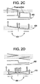
- FIGs. 2a-2d illustrate example embodiments of modified reflective devices 400, 406, 408, and 410, which may be included in an example embodiment of the SLM 1, which may further be included in an example embodiment of an apparatus for patterning a workpiece according to the present invention.
- a reflective device 400 may be a planar micromirror device, which may include at least two portions 400A and 400B. Each of the portions 400A and/or 400B may have an underlying electrode 404. The portions 400A and 400B may each be half of the reflective device 400 and the electrodes 404 may be address and/or counter electrodes.
- the electrodes 404 may manipulate (e.g., tilt and/or deform) the reflective device 400 in a plurality of ways as are discussed herein.
- the reflective devices may reflect radiation (e.g., electromagnetic radiation light waves, etc.) irradiated at the reflective device 400 by the source 2.
- the source 2 may be, for example, an excimer laser, as illustrated in FIG. 1 .
- a phase shifting plate 402 may be positioned, for example, between the reflective device 400 and the substrate 5, which may be, for example, a work piece for patterning.
- the phase shifting plate 402 may induce a phase shift in the radiation reflected by the portion 400A and the radiation reflected by the portion 400B.
- the phase difference between the reflected radiations may be equal, or substantially equal, to half of the wavelength of radiation, ⁇ /2, relative to one another.
- the phase shift plate 402 may be comprised of, for example, quartz glass.
- FIG. 2b illustrates another example embodiment of the present invention, which may be similar to that which has been described with respect to FIG. 2a , however, FIG. 2b may include a reflective device 406.
- Reflective device 406 may be a non-planar mirror or similar reflective surface.
- the reflective device 406 may be, for example, curved, as illustrated in FIG. 2b .
- the phase shifting plate 402 may be positioned, for example, between the reflective device 406 and a substrate (not shown), and may induce a phase difference between the radiation reflected by portions of the reflective device 406.
- the phase difference may be, for example, similar, or substantially similar, to the phase difference as described above with regard to FIG. 2a .
- the phase shift plate 402 may be comprised of, for example, quartz glass, although, the phase shift plate may be comprised of any suitable material.
- FIG. 2c illustrates another example embodiment of the present invention, similar to that which has been described with respect to FIG. 2b , however, FIG. 2c may include a reflective device 408, which may be a tilted non-planar mirror or similar reflective device.
- the reflective device 408 may be, for example, curved and tilted as discussed above and, further, in any way suitable to achieve a desired phase difference.
- a phase shifting plate 402 may be positioned, for example, between the reflective device 408 and a substrate (not shown), and may induce a phase difference between the radiation reflected by two portions of the reflective device 408.
- the phase difference may be similar, or substantially similar, to the phase difference as described above with regard to FIG. 2b .
- Partially coherent reflected light for a mirror may be represented, for example, by a complex amplitude reflection coefficient which, for a tilting micro-mirror, may be obtained by integration over the deflected surface for a given tilt:
- the complex amplitude trajectory in the complex amplitude space may be obtained by connecting all, or substantially all, complex amplitude reflection coefficients for the used mirror deflection angles.
- the mirror may have symmetry, which may balance the average phase, while being deflected in a manner similar or substantially similar, to the way in which any phase modulation in the positive phase direction is counteracted with an equal, or substantially equal, phase modulation in the negative phase direction.
- the average phase may be preserved for all, or substantially all, tilt angles, which may lead to a complex amplitude trajectory on the real valued axis of the complex amplitude space.
- the symmetry may be broken and the complex amplitude trajectory may deviate (e.g., deviate in parts) from the real axis in complex amplitude space.
- An imaginary contribution to the complex amplitude trajectory may be the same, or substantially the same, as having remaining phase information in the final image leading to reduced performance of the lithography system.
- phase step as illustrated in figure 2b and 2c may change the situation, for example, a non-tilted non-planar mirror with a shape that may be described by a mathematically even form with respect to the tilt axis the phase symmetry, may be re-established and the imaginary contributions from the two sides of the mirror may cancel one another. That is, the complex amplitude reflection coefficient may reach 0+0i (i.e., the origin) while maintaining higher contrast in the image.
- the phase step may further reduce the phase content in the final image over the entire complex amplitude trajectory from, for example, a minimum to a maximum intensity, which may result in leading to improved lithographic performance.
- FIG. 2d illustrates another example embodiment of the present invention, similar to that which has been described with respect to FIG. 2a .
- FIG. 2d illustrates a tilted reflective device 410, which may be a planar mirror or similar reflective surface.
- the reflective device 410 may be tilted as discussed above and, further, in any angular direction and magnitude suitable to achieve a desired phase difference.
- a phase shifting plate 402 may be positioned, for example, between the reflective device 410 and a substrate (not shown), and may induce a phase difference between the radiation reflected by two portions of the reflective device 410.
- the phase difference may be similar, or substantially similar, to the phase difference as described above with regard to FIG. 2a .
- the phase shift plate 402 may be comprised of, for example, quartz glass.
- FIG. 3 illustrates an example embodiment of a movable microelement 800, according to the present invention, which may be manufactured using an example embodiment of the method as described above and may be included in the SLM 1 of FIG. 1 .
- the movable microelement 800 may be, for example, a micro mechanical element.
- the movable microelement 800 may be, for example, a reflective element 111 in SLM 1.
- the reflective element 111 may be utilized in an analog mode, for example, to vary a degree of deflection of the reflective element 111 as a function of an electrical input, or, a digital mode, which may represent an ON and/or OFF state of the reflective element 111.
- the ON or OFF state may be defined by increased (e.g., maximum) deflection and/or no, or substantially no, deflection.
- an area 111 which may be similar, or substantially similar to area 100 as described above, may be a rectangular reflective element, which may be supported along at least one mid section by at least one e.g., (a pair) of hinges (e.g., torsional hinges) 60.
- the reflective element 111 may be, for example, polygonal, circular, or elliptical, or any combination thereof.
- the hinges 60 may define an axis (e.g., a torsional axis) there along.
- the hinges 60 may extend from the reflective element 111 and may be supported by a support 50.
- the support 50 may rest on a substrate 20 and the reflective element 111.
- the hinges 60, the support 50 and/or the substrate 20 may be comprised of the same, or substantially the same, material.
- the material may be, for example, silicon, aluminum, another metal or any alloy or other combination thereof and may be, for example, etched out of a substrate, for example, using etching techniques, as desired by one of ordinary skill in the art.
- the substrate 20 may further include an electrode (e.g., an electrically conducting address electrode) 40 and/or an electrode (e.g., an optional electrically conducting counter electrode) 30.
- the electrode 40 and the electrode 30 may be connected to underlying circuitry (e.g., CMOS and/or address circuitry), which may be included in the substrate 20 (not shown).
- the electrodes 30 and/or 40 may be connected to capacitors, which may store the voltage (e.g., address voltage) addressed to the electrode 30 and/or 40.
- the electrode 30 and/or the electrode 40 may be spaced apart (e.g., laterally) on the substrate 20 and may electrostatically attract the reflective element 111.
- the hinges 60 may rotate and/or twist with the reflective element 111 and may provide restoring force in the form of, for example, mechanical energy.
- voltage for example, ground
- the reflective element 111 may be in a flat (e.g., undeflected) position, which may be referred to as an electrically unattracted state.
- the voltage may be shifted from the electrode 40 to the electrode 30 and the reflective element 111 may be rotated in a plurality of angular directions.
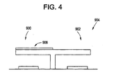
- FIG. 4 illustrates an example embodiment of a modified reflective device 904, according to the present invention.
- Phase shifted addressing may be achieved by manipulating, for example, the shape of the reflective devices on the SLM 1.
- the reflective element 904 may be modified by, for example, forming a layer of material 906, which may correspond to a desired shift of the phase of radiation reflected by a portion of the reflective device or devices 904 by 180 degrees or ⁇ /2.
- the layer of material may be formed using, for example, a deposition process or any other suitable process.
- a layer of material may be subtracted from a portion of the reflective device 904 in another process (e.g., a lithography, process, or any other suitable process), to obtain a desired phase shifting (not shown).
- the reflective device 904 may be formed such that a portion 900 of the surface of the reflective device 904 is, for example, ⁇ /4 higher than another portion 902.
- Phase shifted addressing may enable increased pattern resolution without changing other parameters of, for example, a lithography system or any other suitable system.
- An increased (e.g., full) phase shift may result when shifting (e.g., tilting) a portion (e.g., an edge) of reflective device 904, or 410, for example, between - ⁇ /4 to + ⁇ /4 using the addressing system.
- the addressing system may tilt the reflective device in multiple (e.g., opposite) directions.
- Light or electromagnetic radiation radiating from the different portions of the mirror may differ in phase by ⁇ /2 ⁇ n* ⁇ , where n is a natural number (e.g., 0, 1, 2, ).
- a difference in height of the different portions of the mirror may be ⁇ /4 ⁇ (n* ⁇ /2), where n is a natural number (e.g., 0, 1, 2, ...), although n may also be any suitable number.
- a tilting mirror without the phase step may allow negative amplitude up to approximately -0.2, which may correspond to a negative intensity of about -0,05. This may be sufficient to achieve feature resolution enhancement similar, or substantially similar, to attenuated phase shifting in steppers but may not achieve phase shifting similar, or substantially similar to an alternating phase shift mask.
- phase step mirror may cancel amplitudes from, for example, the two mirror surfaces and may result in reduced (e.g., little or no) intensity (black) for non-deflection.
- Tilting the phase-step mirror one way may provide an amplitude trajectory in the positive real amplitude direction, for example, up to an amplitude of about +0,7 corresponding to an intensity of about +0,5.
- Tilting the phase-step mirror in another direction may provide a negative amplitude of, for example, about -0,7 corresponding to an intensity of about -0,5.
- phase-step mirrors may require twice as much radiation dose as a mirror without phase step, but may allow for stronger phase shifting with preserved grayscaling.
- FIGs. 5a-5e illustrate an example of a method of manufacturing a micro-electrical-mechanical-system (MEMS).
- Figures 5a-5e are examples of cross sections, which may be taken along line A in FIG. 3 .
- a substrate 230 which may be comprised of a semiconductor material (e.g., silicon).
- the substrate 230 may include complementary metal-oxide semiconductor (CMOS) circuitry and areas 210, 212, 214, which may be metal (e.g., aluminum, any alloy thereof, or any suitable metallic element) and areas 220, which may be, for example, silicon dioxide.
- the areas 220 which may be positioned between the areas 210, 212, 214 may separate (e.g., isolate) the areas 210, 212, 214.
- the areas 210 may form connections (e.g., electrical connections) to the reflective elements in, for example, the SLM 1.
- Areas 212 and/or 214 may form connections (e.g., electrical connections) to electrodes (e.g., address electrodes) or they may constitute electrodes themselves.
- a layer 240 (e.g., a temporary layer) may be formed on the areas 210, 212, 214 and/or the areas 220.
- the layer 240 may be comprised of a radiation sensitive material (e.g., electromagnetic radiation sensitive material).
- Stopper 250 may be arranged within the layer 240 and may function as insulation (e.g., electrical insulation) for a reflective element.
- the stopper 250 may separate the reflective elements from the areas 210, 212, and 214 and/or from electrodes, and may reduce the likelihood of a short circuit.
- the stopper may be comprised of a nonconductive or insulating material, for example, silicon dioxide.
- the stopper may also be any suitable insulating material.
- the area 245 disposed between the layers 240 may form support for the reflective element.
- the area 245 may be circular, elliptical, rectangular or any other suitable shape.
- the area 245 between the layers 240 may be provided by, for example, a lithographic process or any other suitable process.
- a layer e.g., a reflective layer
- a layer 260 may be formed on the layers 240, on the areas 245, and/or on the areas 210.
- the layer 280 may be applied and a step height difference within at least one reflective element in the SLM 1 may be formed.
- a layer 270 which may be a photo resist, may be formed on the layer 260 and/or the layer 280.
- a space 285 may separate reflective elements from one another.
- the space 285 may be formed using, for example, any lithographic process or other suitable process, which may involve exposing, developing and/or etching.
- FIG. 5e illustrates an example of an example embodiment of the SLM 1.
- a layer 270 and/or a layer 240 may be removed by, for example, using a liquid solution process, dry etch process, or any other suitable process.
- Figures 6a-6g are examples of cross sections, which may be taken along line B in FIG. 3 .
- the cross sections may relate to the actuator.
- FIG. 6a a cross section of a reflective area 100 of the layer 260 is illustrated, for example, prior to creating a step height difference.
- a layer (e.g., a material layer) 710 may be formed on the layer 260.
- An etch stop layer for example, may be provided between the layer 710 and the layer 260.
- the etch stop layer may be silicon dioxide or any other suitable etch stop material.
- the layer 710 may be formed on the layer 260 by, for example, sputtering or any other conventional method as desired by one of ordinary skill in the art.
- a layer (e.g., a temporary layer) 720 which may be sensitive to radiation (e.g., electromagnetic radiation), may be formed on the layer 710.
- the layer 720 may be, for example, a resist or a photo resist.
- a portion (e.g., half) 722 of the layer 720 may be exposed and a portion (e.g., half) 724 of layer 720 may not be exposed as described above.
- the portion 724 which may be the unexposed portion, of the layer 720 may remain on the layer 710, the portion 722 of the layer 720 may be removed, and a portion of the reflective area 100 may have an uncoated material layer.
- the uncoated portion of the layer 710 may be removed, for example etched away, and layer 720 may be removed from the area 100.
- the etching process may be dry based, wet based, or any other etching process as desired by one of ordinary skill in the art.
- an area 100 may include a portion of the layer 260 with the layer 710 formed thereon.
- the unexposed layer on the portion 724 may be dissolved by a liquid solution.
- the substrate 230 may include a plurality of areas 100 (e.g., reflective areas or pixels), which may form an example embodiment of the SLM 1.
- the substrate 5 may include between 1 million and 10 million areas 100.
- a side of an area 100 may be between 8 microns and 16 microns.
- a step height difference within the area 100 may be formed and a plurality of areas 100 may be separated from one another.
- the area 100 as illustrated in FIG. 7a , may be covered with a layer 110, which may be sensitive to radiation (e.g., electromagnetic radiation).
- layer 110 may be a resist.
- the layer 110 may be formed on the layer 260 according to, for example, any suitable method.
- a portion (e.g., half) 120 of the area 100 may be exposed to a wavelength, to which the layer 110 may be sensitive.
- Another portion (e.g., half) 130 of the area 100 may not be exposed. Exposure may be done according to any suitable method, for example, using an electron beam pattern generator or a laser pattern generator, in which an electron beam (e-beam) or a laser beam may be scanned over the surface of the substrate, or a stepper using a photo mask.
- the layer 110 may be exposed and remain on the portion 120 of the area 100 and layer 110 may be removed from the portion 130 of the area 100.
- a positive resist may be used such that the layer 110 may remain on the portion 130 of the area 100, for example, during developing.
- a portion 150 and a portion 160 may be covered with a material layer (denoted by hexagonal mosaic).
- the material layer may be formed by, for example, sputtering or any suitable process.
- the material layer may be formed on the exposed layer 110.
- the material layer may be formed on the layer 260.
- the material layer may have a thickness, which may be equal, or substantially equal, to a quarter of the wavelength of the radiation ⁇ /4.
- the material layer thickness may also be any suitable thickness.
- the wavelength may be, for example, 248 nm and the thickness of the material layer, which may be sputtered onto the area 100, may be, for example, 62 nm. If a different wavelength is used, another step height difference between the portions, for example, portions 150 and 160 of the area 100 may be used.
- the material layer which may be formed on the layer 110, may be removed in, for example, a lift-off process or any other suitable process.
- the portion 170 of the area 100 may be an uncovered portion of the area 100 and the portion 160 may be covered with the material layer.
- a step height between the portion 160 and the portion 170 of the reflective area 100 may be varied as desired according to the material, which creates the step height difference.
- Example embodiments of the present invention may improve writing quality in, for example, a micro lithography system, which may use a Spatial Light Modulator (SLM).
- SLM Spatial Light Modulator
- Example embodiments of the present invention may also improve the writing quality in, for example, micro-lithography systems, which may include reflective devices (e.g., mirrors, micromirrors, etc.), which are non-planar.
- Example embodiments of the present invention may also improve writing quality in any other suitable system.
- a substrate as described herein, may be comprised of any suitable material (e.g., glass, ceramic, metal, metal alloy, etc.) as desired by one of ordinary skill in the art.
- suitable material e.g., glass, ceramic, metal, metal alloy, etc.
- UV light ultra violet (UV) light
- EUV extreme ultra violet
Description
- Example embodiments of the present invention relate to lithography.
- In conventional lithography systems, a spatial light modulator (SLM) may be used in pattern generation. Conventional SLM's may include tilting planar micromirrors. The micromirrors may be tilted in order to generate a pattern on a work piece. The writing quality of the conventional lithography systems may depend on the degree of planarity of the micromirrors. For example, the planarity of the micromirrors may decrease and the writing quality may decrease as a result thereof. An increase in the planarity of one or more micromirrors may provide for higher quality pattern generation. For example, one or more micromirrors may have a greater degree of planarity, and writing quality may improve. However, higher degrees of planarity (e.g., extreme or perfect planarity) may be difficult to achieve and/or cost ineffective.
- Conventional tilting micro-mirrors may also have a reduced amount of negative amplitude. Negative amplitude may be useful since in enabling resolution enhancements. For example, full, or substantially full, negative amplitude may be used in chromeless phase lithography on masks in, for example, stepper technology. Full, or substantially full, negative amplitude may enable stronger phase shift effects, which may result in resolution enhancements.
Spartial light modulations introducing phase shift effects are disclosed inUS 6 489 984 B1 and inUS 6 285 488 B1 . - The present invention provides a spatial light modulator according to claim 1 and a method for patterning a workpiece according to claim 11.
- In example embodiments of the present invention, introducing a phase difference in the electromagnetic radiation from tilting micro-mirrors may extend the addressable amplitude domain to encompass, for example, full, or substantially full, negative amplitude in addition to full, or substantially full, positive amplitude. This may enable full, or substantially full, phase-shift resolution enhancement techniques.
- In example embodiments of the present invention, the phase difference between the at least two portions of the radiation at the workpiece may be half of a wavelength of the radiation or, for example, λ/2±n*λ, where λ is the wave length of the electromagnetic radiation and n is a natural number (e.g., 0, 1, 2, ...).
- In example embodiments of the present invention, the phase step height difference may be a quarter of the wavelength of the radiation or λ/4±(n*λ/2), where λ is the wave length of the electromagnetic radiation and n is a natural number (e.g., 0, 1, 2, ...).
- In example embodiments of the present invention, the at least one mirror may be a planar or a non-planar mirror.
- In example embodiments of the present invention, the plurality of reflective surfaces may be tiltable.
- In example embodiments of the present invention, the radiation may be electromagnetic radiation and/or at least one of ultra violet and extreme ultra violet radiation.
- In example embodiments of the present invention, the at least one phase plate may be transmissive or reflective.
- In example embodiments of the present invention, the at least two portions of the at least one of the plurality of reflective surfaces may be adjacent.
- In example embodiments of the present invention, the radiation may be in the form of light waves.
- In example embodiments of the present invention, the step height of the first portion may differ from the step height of the second portion by a value, which may be equal, or substantially equal, to, for example, a quarter of the wavelength of the radiation.
- Example embodiments of the present invention will become more apparent with reference to the attached drawings in which:
-
FIG. 1 illustrates an example embodiment of an apparatus for patterning a workpiece, according to the present invention; -
FIGs. 2a-2d illustrate example embodiments of modified reflective devices according to the present invention; -
FIG. 3 illustrates another example embodiment of a reflective device, according to the present invention; -
FIG. 4 illustrates another example embodiment of a reflective device, according to the present invention, which may include a step height difference; -
FIGs. 5a-5e illustrate an example not forming part of the present invention of a method of manufacture viewed as a cross-section taken along line A ofFIG. 3 ; -
FIGs. 6a-6g illustrate an example not forming part of the present invention of a method of manufacture viewed as a cross-section taken along line B ofFIG. 3 ; and -
FIGs. 7a-7e illustrate a top view of an example not forming part of the present invention of the method of manufacture. - Example embodiments of the present invention will be described more fully with reference to the accompanying drawings, in which example embodiments of the invention are shown. It should be understood, however, that example embodiments of the present invention described herein can be modified in form and detail without departing from the scope of the invention. Accordingly, the example embodiments described herein are provided by way of example and not of limitation, and the scope of the present invention is not restricted to the particular embodiments described herein.
- In particular, the relative thicknesses and positioning of layers or regions may be reduced or exaggerated for clarity. Further, a layer is considered as being formed "on" another layer or a substrate when formed either directly on the referenced layer or the substrate or formed on other layers or patterns overlaying the referenced layer.
- Referring to
FIG. 1 , a system for generating a pattern on a work piece may include a pattern generator according to an example embodiment of the present invention. The pattern generator may comprise an SLM 1, which may include individual and/or multi-value pixel addressing, asource 2, an imaging system (e.g., an imaging optical system) 3, and a hardware and/or softwaredata handling system 4. The system may further include a stage 5, for example, with acontrol system 6. - The SLM 1 may include reflective devices (i.e., micromachined mirrors or micromirrors). Reflective SLMs may rely on, for example, micromechanical SLMs. The micromechanical SLMs may use piezoelectric and/or electrostrictive actuation.
- The SLM 1 may be irradiated by a
source 2. Thesource 2 may be a KrF excimer laser, which may provide a 10-20 nanoseconds long radiation flash in the UV region at 248 nanometer wavelength, and may have a bandwidth corresponding to the natural linewidth of an excimer laser. To reduce pattern distortion on the substrate, the radiation from thesource 2 may be distributed (e.g., uniformly distributed) over the surface of the SLM 1 surface and the light may have a coherent length, which may not produce laser speckle on the substrate 5. - The system of
Fig. 1 may have a stage (e.g., a fine positioning substrate stage) 5 and may include a control system (e.g., an interferometer position control system) 6. In a first direction (e.g., the γ-direction (not shown)) a mechanical system (e.g., a servo system) may keep the stage in a position and in second direction (e.g., the x-direction), which may be perpendicular to the first direction, the stage may move (e.g., mechanically move) with, for example, continuous speed. Thecontrol system 6, which may be used in the x-direction to trigger the exposure laser flashes, may provide uniform, or substantially uniform, position between images of the SLM 1 on the substrate 5. When a row of SLM images are exposed on the substrate 5, the substrate 5 may return to an original position in the x-direction and may move one SLM image increment in the-y direction and expose another row of SLM images on the substrate 5. This procedure may be repeated until the all, or substantially all, of the images on the substrate 5 may be exposed. The surface may be written in, for example, several passes and may average out errors. - The SLM 1 may include a plurality of reflective devices (e.g., micromirrors). The reflective devices may be manipulated (e.g., electrically) to reflect and/or diffract incoming radiation in a plurality of directions depending on a voltage, which may be applied (e.g., individually) to the reflective devices.
- An example embodiment of the present invention may provide a method for modifying the shape of the reflective devices (e.g., micromirrors), which may achieve, for example, phase shifted addressing. The modified reflective devices may be used in example embodiments of the SLM 1, as described above with regard to
FIG. 1 . For example, example embodiments of the present invention provide a method of manufacturing a step height difference within a reflective device of an example embodiment of the SLM 1. -
FIGs. 2a-2d illustrate example embodiments of modifiedreflective devices FIG. 2a , areflective device 400 may be a planar micromirror device, which may include at least twoportions portions 400A and/or 400B may have anunderlying electrode 404. Theportions reflective device 400 and theelectrodes 404 may be address and/or counter electrodes. - The
electrodes 404 may manipulate (e.g., tilt and/or deform) thereflective device 400 in a plurality of ways as are discussed herein. The reflective devices may reflect radiation (e.g., electromagnetic radiation light waves, etc.) irradiated at thereflective device 400 by thesource 2. Thesource 2 may be, for example, an excimer laser, as illustrated inFIG. 1 . Aphase shifting plate 402 may be positioned, for example, between thereflective device 400 and the substrate 5, which may be, for example, a work piece for patterning. Thephase shifting plate 402 may induce a phase shift in the radiation reflected by theportion 400A and the radiation reflected by theportion 400B. The phase difference between the reflected radiations may be equal, or substantially equal, to half of the wavelength of radiation, λ/2, relative to one another. Thephase shift plate 402 may be comprised of, for example, quartz glass. -
FIG. 2b illustrates another example embodiment of the present invention, which may be similar to that which has been described with respect toFIG. 2a , however,FIG. 2b may include areflective device 406.Reflective device 406 may be a non-planar mirror or similar reflective surface. Thereflective device 406 may be, for example, curved, as illustrated inFIG. 2b . Thephase shifting plate 402 may be positioned, for example, between thereflective device 406 and a substrate (not shown), and may induce a phase difference between the radiation reflected by portions of thereflective device 406. The phase difference may be, for example, similar, or substantially similar, to the phase difference as described above with regard toFIG. 2a . Thephase shift plate 402 may be comprised of, for example, quartz glass, although, the phase shift plate may be comprised of any suitable material. -
FIG. 2c illustrates another example embodiment of the present invention, similar to that which has been described with respect toFIG. 2b , however,FIG. 2c may include areflective device 408, which may be a tilted non-planar mirror or similar reflective device. Thereflective device 408 may be, for example, curved and tilted as discussed above and, further, in any way suitable to achieve a desired phase difference. Aphase shifting plate 402 may be positioned, for example, between thereflective device 408 and a substrate (not shown), and may induce a phase difference between the radiation reflected by two portions of thereflective device 408. The phase difference may be similar, or substantially similar, to the phase difference as described above with regard toFIG. 2b . - Partially coherent reflected light for a mirror may be represented, for example, by a complex amplitude reflection coefficient which, for a tilting micro-mirror, may be obtained by integration over the deflected surface for a given tilt:
-

- where S is the surface of the mirror, λ is the wavelength, h is the local height and r is the local reflection. An intensity contribution from a mirror may be given by the square of the complex amplitude reflection coefficient for a given deflection. The complex amplitude trajectory in the complex amplitude space may be obtained by connecting all, or substantially all, complex amplitude reflection coefficients for the used mirror deflection angles. For example, for a flat tilting mirror with the tilt axis in balance, i.e. in the center of the mirror, the mirror may have symmetry, which may balance the average phase, while being deflected in a manner similar or substantially similar, to the way in which any phase modulation in the positive phase direction is counteracted with an equal, or substantially equal, phase modulation in the negative phase direction. The average phase may be preserved for all, or substantially all, tilt angles, which may lead to a complex amplitude trajectory on the real valued axis of the complex amplitude space. For any non-planarity of the mirror the symmetry may be broken and the complex amplitude trajectory may deviate (e.g., deviate in parts) from the real axis in complex amplitude space. Reaching the point R=0+0i (i.e., the origin) in the complex amplitude space for a non-planar mirror may not be possible without a phase step. An imaginary contribution to the complex amplitude trajectory may be the same, or substantially the same, as having remaining phase information in the final image leading to reduced performance of the lithography system. Available contrast may also be affected since the complex amplitude reflection coefficient may not reach 0+0i (i.e., the origin), and the intensity may not reach zero (=black) for any mirror deflection angle, for example, when a mirror without a phase step is non-flat (e.g., when the mirror is curved).
- Introducing a phase step as illustrated in
figure 2b and2c may change the situation, for example, a non-tilted non-planar mirror with a shape that may be described by a mathematically even form with respect to the tilt axis the phase symmetry, may be re-established and the imaginary contributions from the two sides of the mirror may cancel one another. That is, the complex amplitude reflection coefficient may reach 0+0i (i.e., the origin) while maintaining higher contrast in the image. The phase step may further reduce the phase content in the final image over the entire complex amplitude trajectory from, for example, a minimum to a maximum intensity, which may result in leading to improved lithographic performance. -
FIG. 2d illustrates another example embodiment of the present invention, similar to that which has been described with respect toFIG. 2a .FIG. 2d illustrates a tiltedreflective device 410, which may be a planar mirror or similar reflective surface. Thereflective device 410 may be tilted as discussed above and, further, in any angular direction and magnitude suitable to achieve a desired phase difference. Aphase shifting plate 402 may be positioned, for example, between thereflective device 410 and a substrate (not shown), and may induce a phase difference between the radiation reflected by two portions of thereflective device 410. The phase difference may be similar, or substantially similar, to the phase difference as described above with regard toFIG. 2a . Thephase shift plate 402 may be comprised of, for example, quartz glass. -
FIG. 3 illustrates an example embodiment of amovable microelement 800, according to the present invention, which may be manufactured using an example embodiment of the method as described above and may be included in the SLM 1 ofFIG. 1 . Themovable microelement 800 may be, for example, a micro mechanical element. Themovable microelement 800 may be, for example, areflective element 111 in SLM 1. Thereflective element 111 may be utilized in an analog mode, for example, to vary a degree of deflection of thereflective element 111 as a function of an electrical input, or, a digital mode, which may represent an ON and/or OFF state of thereflective element 111. The ON or OFF state may be defined by increased (e.g., maximum) deflection and/or no, or substantially no, deflection. In example embodiments of the present invention, anarea 111, which may be similar, or substantially similar toarea 100 as described above, may be a rectangular reflective element, which may be supported along at least one mid section by at least one e.g., (a pair) of hinges (e.g., torsional hinges) 60. - The
reflective element 111 may be, for example, polygonal, circular, or elliptical, or any combination thereof. The hinges 60 may define an axis (e.g., a torsional axis) there along. The hinges 60 may extend from thereflective element 111 and may be supported by asupport 50. Thesupport 50 may rest on asubstrate 20 and thereflective element 111. The hinges 60, thesupport 50 and/or thesubstrate 20 may be comprised of the same, or substantially the same, material. The material may be, for example, silicon, aluminum, another metal or any alloy or other combination thereof and may be, for example, etched out of a substrate, for example, using etching techniques, as desired by one of ordinary skill in the art. Thesubstrate 20 may further include an electrode (e.g., an electrically conducting address electrode) 40 and/or an electrode (e.g., an optional electrically conducting counter electrode) 30. Theelectrode 40 and theelectrode 30 may be connected to underlying circuitry (e.g., CMOS and/or address circuitry), which may be included in the substrate 20 (not shown). Theelectrodes 30 and/or 40 may be connected to capacitors, which may store the voltage (e.g., address voltage) addressed to theelectrode 30 and/or 40. - The
electrode 30 and/or theelectrode 40 may be spaced apart (e.g., laterally) on thesubstrate 20 and may electrostatically attract thereflective element 111. The hinges 60 may rotate and/or twist with thereflective element 111 and may provide restoring force in the form of, for example, mechanical energy. When the same, or substantially the same, voltage, for example, ground, is applied on thereflective element 111, by theelectrode 30 and/or theelectrode 40, thereflective element 111 may be in a flat (e.g., undeflected) position, which may be referred to as an electrically unattracted state. The voltage may be shifted from theelectrode 40 to theelectrode 30 and thereflective element 111 may be rotated in a plurality of angular directions. -
FIG. 4 illustrates an example embodiment of a modifiedreflective device 904, according to the present invention. Phase shifted addressing may be achieved by manipulating, for example, the shape of the reflective devices on the SLM 1. Thereflective element 904 may be modified by, for example, forming a layer ofmaterial 906, which may correspond to a desired shift of the phase of radiation reflected by a portion of the reflective device ordevices 904 by 180 degrees or λ/2. The layer of material may be formed using, for example, a deposition process or any other suitable process. In another example embodiment of the present invention, a layer of material may be subtracted from a portion of thereflective device 904 in another process (e.g., a lithography, process, or any other suitable process), to obtain a desired phase shifting (not shown). Thereflective device 904 may be formed such that aportion 900 of the surface of thereflective device 904 is, for example, λ/4 higher than anotherportion 902. - Phase shifted addressing may enable increased pattern resolution without changing other parameters of, for example, a lithography system or any other suitable system. An increased (e.g., full) phase shift may result when shifting (e.g., tilting) a portion (e.g., an edge) of
reflective device - With a phase step mirror the phase step may cancel amplitudes from, for example, the two mirror surfaces and may result in reduced (e.g., little or no) intensity (black) for non-deflection. Tilting the phase-step mirror one way may provide an amplitude trajectory in the positive real amplitude direction, for example, up to an amplitude of about +0,7 corresponding to an intensity of about +0,5. Tilting the phase-step mirror in another direction may provide a negative amplitude of, for example, about -0,7 corresponding to an intensity of about -0,5. Thus, for example, phase-step mirrors may require twice as much radiation dose as a mirror without phase step, but may allow for stronger phase shifting with preserved grayscaling.
-
FIGs. 5a-5e illustrate an example of a method of manufacturing a micro-electrical-mechanical-system (MEMS).Figures 5a-5e are examples of cross sections, which may be taken along line A inFIG. 3 . - With regard to
FIG. 5a , asubstrate 230, which may be comprised of a semiconductor material (e.g., silicon). Thesubstrate 230 may include complementary metal-oxide semiconductor (CMOS) circuitry andareas areas 220, which may be, for example, silicon dioxide. Theareas 220, which may be positioned between theareas areas areas 210 may form connections (e.g., electrical connections) to the reflective elements in, for example, the SLM 1.Areas 212 and/or 214 may form connections (e.g., electrical connections) to electrodes (e.g., address electrodes) or they may constitute electrodes themselves. - With regard to
FIG. 5b , a layer 240 (e.g., a temporary layer) may be formed on theareas areas 220. Thelayer 240 may be comprised of a radiation sensitive material (e.g., electromagnetic radiation sensitive material).Stopper 250 may be arranged within thelayer 240 and may function as insulation (e.g., electrical insulation) for a reflective element. Thestopper 250 may separate the reflective elements from theareas - The
area 245 disposed between thelayers 240 may form support for the reflective element. For example, thearea 245 may be circular, elliptical, rectangular or any other suitable shape. Thearea 245 between thelayers 240 may be provided by, for example, a lithographic process or any other suitable process. - With regard to
FIG. 5c , a layer (e.g., a reflective layer) 260 may be formed on thelayers 240, on theareas 245, and/or on theareas 210. - The
layer 280 may be applied and a step height difference within at least one reflective element in the SLM 1 may be formed. - With regard to
FIG. 5d , for example, alayer 270, which may be a photo resist, may be formed on thelayer 260 and/or thelayer 280. Aspace 285 may separate reflective elements from one another. Thespace 285 may be formed using, for example, any lithographic process or other suitable process, which may involve exposing, developing and/or etching. -
FIG. 5e illustrates an example of an example embodiment of the SLM 1. Alayer 270 and/or alayer 240 may be removed by, for example, using a liquid solution process, dry etch process, or any other suitable process. -
Figures 6a-6g are examples of cross sections, which may be taken along line B inFIG. 3 . The cross sections may relate to the actuator. - With regard to
FIG. 6a , a cross section of areflective area 100 of thelayer 260 is illustrated, for example, prior to creating a step height difference. - With regard to
FIG. 6b , a layer (e.g., a material layer) 710 may be formed on thelayer 260. An etch stop layer, for example, may be provided between thelayer 710 and thelayer 260. The etch stop layer may be silicon dioxide or any other suitable etch stop material. Thelayer 710 may be formed on thelayer 260 by, for example, sputtering or any other conventional method as desired by one of ordinary skill in the art. - With regard to
FIG. 6c , a layer (e.g., a temporary layer) 720, which may be sensitive to radiation (e.g., electromagnetic radiation), may be formed on thelayer 710. Thelayer 720 may be, for example, a resist or a photo resist. With regard toFIG. 6d , a portion (e.g., half) 722 of thelayer 720 may be exposed and a portion (e.g., half) 724 oflayer 720 may not be exposed as described above. - With regard to
FIG. 6e , theportion 724, which may be the unexposed portion, of thelayer 720 may remain on thelayer 710, theportion 722 of thelayer 720 may be removed, and a portion of thereflective area 100 may have an uncoated material layer. - With regard to
FIG. 6f , the uncoated portion of thelayer 710 may be removed, for example etched away, andlayer 720 may be removed from thearea 100. The etching process may be dry based, wet based, or any other etching process as desired by one of ordinary skill in the art. - With regard to
FIG. 6g , anarea 100 may include a portion of thelayer 260 with thelayer 710 formed thereon. The unexposed layer on theportion 724 may be dissolved by a liquid solution. - With regard to
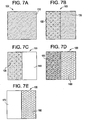
FIG. 7a , thesubstrate 230 may include a plurality of areas 100 (e.g., reflective areas or pixels), which may form an example embodiment of the SLM 1. For example, the substrate 5 may include between 1 million and 10 millionareas 100. A side of anarea 100 may be between 8 microns and 16 microns. A step height difference within thearea 100 may be formed and a plurality ofareas 100 may be separated from one another. Thearea 100, as illustrated inFIG. 7a , may be covered with alayer 110, which may be sensitive to radiation (e.g., electromagnetic radiation). For example,layer 110 may be a resist. Thelayer 110 may be formed on thelayer 260 according to, for example, any suitable method. - With regard to
FIG. 7b , a portion (e.g., half) 120 of thearea 100 may be exposed to a wavelength, to which thelayer 110 may be sensitive. Another portion (e.g., half) 130 of thearea 100 may not be exposed. Exposure may be done according to any suitable method, for example, using an electron beam pattern generator or a laser pattern generator, in which an electron beam (e-beam) or a laser beam may be scanned over the surface of the substrate, or a stepper using a photo mask. - With regard to
FIG. 7c , thelayer 110 may be exposed and remain on theportion 120 of thearea 100 andlayer 110 may be removed from theportion 130 of thearea 100. For example, a positive resist may be used such that thelayer 110 may remain on theportion 130 of thearea 100, for example, during developing. - With regard to
FIG. 7d , aportion 150 and aportion 160 may be covered with a material layer (denoted by hexagonal mosaic). The material layer may be formed by, for example, sputtering or any suitable process. In theportion 150 of thearea 100, the material layer may be formed on the exposedlayer 110. In theother portion 160 of the reflective area, the material layer may be formed on thelayer 260. The material layer may have a thickness, which may be equal, or substantially equal, to a quarter of the wavelength of the radiation λ/4. The material layer thickness may also be any suitable thickness. For example, if an example embodiment of the SLM 1 is to be used as a modulator in a pattern generator, the wavelength may be, for example, 248 nm and the thickness of the material layer, which may be sputtered onto thearea 100, may be, for example, 62 nm. If a different wavelength is used, another step height difference between the portions, for example,portions area 100 may be used. - With regard to
FIG. 7e , the material layer, which may be formed on thelayer 110, may be removed in, for example, a lift-off process or any other suitable process. Theportion 170 of thearea 100 may be an uncovered portion of thearea 100 and theportion 160 may be covered with the material layer. A step height between theportion 160 and theportion 170 of thereflective area 100 may be varied as desired according to the material, which creates the step height difference. - Example embodiments of the present invention may improve writing quality in, for example, a micro lithography system, which may use a Spatial Light Modulator (SLM). Example embodiments of the present invention may also improve the writing quality in, for example, micro-lithography systems, which may include reflective devices (e.g., mirrors, micromirrors, etc.), which are non-planar. Example embodiments of the present invention may also improve writing quality in any other suitable system.
- In example embodiments of the present invention, it will be understood that a substrate, as described herein, may be comprised of any suitable material (e.g., glass, ceramic, metal, metal alloy, etc.) as desired by one of ordinary skill in the art.
- Although example embodiments of the present invention have been described with regard to ultra violet (UV) light, it will be understood that any suitable light, which may have any suitable wavelength including extreme ultra violet (EUV), may be utilized by one of ordinary skill in the art.
- While the present invention has been particularly shown and described with reference to example embodiments thereof, it will be understood by those of ordinary skill in the art that various changes in form and details may be made therein without departing from the scope of the present invention as defined by the following claims.
Claims (15)
- A spatial light modulator (1), comprising:a plurality of reflective surfaces;characterised in that at least one of the plurality of reflective surfaces is a movable mirror (111, 400, 410, 800, 904) including at least two portions (400A, 400B, 900, 902), wherein the at least two portions are areas within the movable mirror (111, 400, 410, 800, 904), and wherein the at least two portions within the movable mirror are adapted to induce a phase difference between radiation reflected by the at least two portions, the phase difference is induced by at least one of a phase plate (402) and a step height difference (906) between the at least two portions of the movable mirror.
- The spatial light modulator of claim 1, wherein the phase difference between the at least two portions is λ/2±n*λ, where λ is a wavelength of the radiation and n is a natural number.
- The spatial light modulator of claim 1, wherein the step height difference is λ/4±(n*λ/2), where λ is a wavelength of the radiation and n is a natural number.
- The spatial light modulator of claim 1, wherein the at least one movable mirror is a planar mirror.
- The spatial light modulator of claim 1, wherein the at least one movable mirror is a non-planar mirror.
- The spatial light modulator of claim 1, wherein the plurality of reflective surfaces are tiltable.
- The spatial light modulator of claim 1, wherein the radiation is electromagnetic radiation.
- The spatial light modulator of claim 7, wherein the radiation is at least one of ultra violet and extreme ultra violet radiation.
- The apparatus of claim 1, wherein the at least one phase plate is transmissive or reflective.
- The apparatus of claim 1, wherein the at least two portions of the at least one movable mirror are adjacent.
- A method for patterning a workpiece including:generating radiation, including at least a first portion and at least a second portion,reflecting at least the first portion and the second portion of the radiation toward the workpiece;irradiating at least the first portion and the second portion of the reflected radiation at the workpiece; andforming a pattern on the workpiece by using at least the first and the second portions of the reflected radiation characterised in that the first portion of the radiation is reflected from a first portion (400A, 900) of a movable mirror (111, 400, 410, 800, 904) and the second portion of the radiation is reflected from a second portion (400B, 902) of the same movable mirror, wherein a phase difference between the first and the second portions of the radiation is induced by at least one of a phase plate (402) and a step height difference (906) within the movable mirror.
- The method of claim 11, wherein the phase of the first portion differs from the phase of the second portion by λ/2±n*λ, where λ is a wavelength of the radiation and n is a natural number.
- The method of claim 11, wherein the phase of the first portion differs from the phase of the second portion by λ/4±(n*λ/2), where λ is a wavelength of the radiation and n is a natural number.
- The method of claim 11, wherein the radiation is electromagnetic radiation.
- The method of claim 14, wherein the radiation is in the form of light waves.
Applications Claiming Priority (4)
| Application Number | Priority Date | Filing Date | Title |
|---|---|---|---|
| US52848803P | 2003-12-11 | 2003-12-11 | |
| US52911403P | 2003-12-15 | 2003-12-15 | |
| US53788704P | 2004-01-22 | 2004-01-22 | |
| PCT/SE2004/001848 WO2005057291A1 (en) | 2003-12-11 | 2004-12-10 | Method and apparatus for patterning a workpiece and methods of manufacturing the same |
Publications (2)
| Publication Number | Publication Date |
|---|---|
| EP1706792A1 EP1706792A1 (en) | 2006-10-04 |
| EP1706792B1 true EP1706792B1 (en) | 2012-11-14 |
Family
ID=34682172
Family Applications (1)
| Application Number | Title | Priority Date | Filing Date |
|---|---|---|---|
| EP04820335A Active EP1706792B1 (en) | 2003-12-11 | 2004-12-10 | Spatial light modulator and method for patterning a workpiece |
Country Status (5)
| Country | Link |
|---|---|
| US (1) | US7110159B2 (en) |
| EP (1) | EP1706792B1 (en) |
| JP (2) | JP4464971B2 (en) |
| KR (1) | KR100797433B1 (en) |
| WO (1) | WO2005057291A1 (en) |
Families Citing this family (30)
| Publication number | Priority date | Publication date | Assignee | Title |
|---|---|---|---|---|
| US7417783B2 (en) * | 2004-09-27 | 2008-08-26 | Idc, Llc | Mirror and mirror layer for optical modulator and method |
| US7373026B2 (en) * | 2004-09-27 | 2008-05-13 | Idc, Llc | MEMS device fabricated on a pre-patterned substrate |
| US7327510B2 (en) * | 2004-09-27 | 2008-02-05 | Idc, Llc | Process for modifying offset voltage characteristics of an interferometric modulator |
| US7420728B2 (en) * | 2004-09-27 | 2008-09-02 | Idc, Llc | Methods of fabricating interferometric modulators by selectively removing a material |
| US7369296B2 (en) | 2004-09-27 | 2008-05-06 | Idc, Llc | Device and method for modifying actuation voltage thresholds of a deformable membrane in an interferometric modulator |
| US7499146B2 (en) * | 2005-03-14 | 2009-03-03 | Asml Netherlands B.V. | Lithographic apparatus and device manufacturing method, an integrated circuit, a flat panel display, and a method of compensating for cupping |
| EP2495212A3 (en) * | 2005-07-22 | 2012-10-31 | QUALCOMM MEMS Technologies, Inc. | Mems devices having support structures and methods of fabricating the same |
| US20070153249A1 (en) * | 2005-12-20 | 2007-07-05 | Asml Netherlands B.V. | Lithographic apparatus and device manufacturing method using multiple exposures and multiple exposure types |
| US7528932B2 (en) * | 2005-12-21 | 2009-05-05 | Micronic Laser Systems Ab | SLM direct writer |
| US7382515B2 (en) | 2006-01-18 | 2008-06-03 | Qualcomm Mems Technologies, Inc. | Silicon-rich silicon nitrides as etch stops in MEMS manufacture |
| US7652814B2 (en) | 2006-01-27 | 2010-01-26 | Qualcomm Mems Technologies, Inc. | MEMS device with integrated optical element |
| US7643203B2 (en) * | 2006-04-10 | 2010-01-05 | Qualcomm Mems Technologies, Inc. | Interferometric optical display system with broadband characteristics |
| US7711239B2 (en) | 2006-04-19 | 2010-05-04 | Qualcomm Mems Technologies, Inc. | Microelectromechanical device and method utilizing nanoparticles |
| US7369292B2 (en) * | 2006-05-03 | 2008-05-06 | Qualcomm Mems Technologies, Inc. | Electrode and interconnect materials for MEMS devices |
| US8052289B2 (en) * | 2006-06-07 | 2011-11-08 | Asml Netherlands B.V. | Mirror array for lithography |
| DE102006057568A1 (en) * | 2006-11-28 | 2008-05-29 | Micronic Laser Systems Ab | Microoptical element with a substrate and method for its production |
| DE102006057567B4 (en) * | 2006-11-28 | 2008-09-04 | Micronic Laser Systems Ab | Microoptical element with a substrate on which at least one height level is formed on an optically active surface, process for its preparation and uses |
| US7706042B2 (en) | 2006-12-20 | 2010-04-27 | Qualcomm Mems Technologies, Inc. | MEMS device and interconnects for same |
| US7733552B2 (en) | 2007-03-21 | 2010-06-08 | Qualcomm Mems Technologies, Inc | MEMS cavity-coating layers and methods |
| US7719752B2 (en) | 2007-05-11 | 2010-05-18 | Qualcomm Mems Technologies, Inc. | MEMS structures, methods of fabricating MEMS components on separate substrates and assembly of same |
| US8068268B2 (en) | 2007-07-03 | 2011-11-29 | Qualcomm Mems Technologies, Inc. | MEMS devices having improved uniformity and methods for making them |
| NL1036334A1 (en) * | 2007-12-28 | 2009-06-30 | Asml Netherlands Bv | SLM calibration. |
| US7863079B2 (en) | 2008-02-05 | 2011-01-04 | Qualcomm Mems Technologies, Inc. | Methods of reducing CD loss in a microelectromechanical device |
| WO2009130603A2 (en) * | 2008-04-24 | 2009-10-29 | Micronic Laser Systems Ab | Spatial light modulator with structured mirror surfaces |
| WO2012039353A1 (en) * | 2010-09-22 | 2012-03-29 | 株式会社ニコン | Spatial light modulator, exposure apparatus, and method for manufacturing device |
| US8659816B2 (en) | 2011-04-25 | 2014-02-25 | Qualcomm Mems Technologies, Inc. | Mechanical layer and methods of making the same |
| JP5953657B2 (en) * | 2011-05-17 | 2016-07-20 | 株式会社ニコン | Spatial light modulator, exposure apparatus, and device manufacturing method |
| JP5973207B2 (en) * | 2012-03-30 | 2016-08-23 | 株式会社オーク製作所 | Maskless exposure system |
| KR102212359B1 (en) | 2013-03-15 | 2021-02-03 | 마이크로닉 아베 | Driver for acoustooptic modulator and modulation principle |
| JP6593623B2 (en) * | 2015-03-30 | 2019-10-23 | 株式会社ニコン | Spatial light modulator setting method, drive data creation method, exposure apparatus, exposure method, and device manufacturing method |
Citations (2)
| Publication number | Priority date | Publication date | Assignee | Title |
|---|---|---|---|---|
| US6285488B1 (en) * | 1998-03-02 | 2001-09-04 | Micronic Laser Systems Ab | Pattern generator for avoiding stitching errors |
| US6489984B1 (en) * | 1998-12-29 | 2002-12-03 | Kenneth C. Johnson | Pixel cross talk suppression in digital microprinters |
Family Cites Families (6)
| Publication number | Priority date | Publication date | Assignee | Title |
|---|---|---|---|---|
| US5446587A (en) | 1992-09-03 | 1995-08-29 | Samsung Electronics Co., Ltd. | Projection method and projection system and mask therefor |
| JPH06102459A (en) * | 1992-09-17 | 1994-04-15 | Dainippon Screen Mfg Co Ltd | Optical modulator and image recorder with the same |
| EP0657760A1 (en) * | 1993-09-15 | 1995-06-14 | Texas Instruments Incorporated | Image simulation and projection system |
| US6624880B2 (en) | 2001-01-18 | 2003-09-23 | Micronic Laser Systems Ab | Method and apparatus for microlithography |
| JP4022398B2 (en) | 2001-12-27 | 2007-12-19 | 株式会社 液晶先端技術開発センター | Method and apparatus for creating phase shift mask |
| JP2005116609A (en) * | 2003-10-03 | 2005-04-28 | Nikon Corp | Image projection equipment and image indication element |
-
2004
- 2004-12-10 JP JP2006543778A patent/JP4464971B2/en not_active Expired - Fee Related
- 2004-12-10 EP EP04820335A patent/EP1706792B1/en active Active
- 2004-12-10 US US11/008,566 patent/US7110159B2/en active Active
- 2004-12-10 WO PCT/SE2004/001848 patent/WO2005057291A1/en active Application Filing
- 2004-12-10 KR KR1020067010959A patent/KR100797433B1/en active IP Right Grant
-
2009
- 2009-12-16 JP JP2009285070A patent/JP5047259B2/en active Active
Patent Citations (2)
| Publication number | Priority date | Publication date | Assignee | Title |
|---|---|---|---|---|
| US6285488B1 (en) * | 1998-03-02 | 2001-09-04 | Micronic Laser Systems Ab | Pattern generator for avoiding stitching errors |
| US6489984B1 (en) * | 1998-12-29 | 2002-12-03 | Kenneth C. Johnson | Pixel cross talk suppression in digital microprinters |
Also Published As
| Publication number | Publication date |
|---|---|
| JP4464971B2 (en) | 2010-05-19 |
| EP1706792A1 (en) | 2006-10-04 |
| KR20060092282A (en) | 2006-08-22 |
| WO2005057291A1 (en) | 2005-06-23 |
| US20050128565A1 (en) | 2005-06-16 |
| JP5047259B2 (en) | 2012-10-10 |
| JP2007522485A (en) | 2007-08-09 |
| KR100797433B1 (en) | 2008-01-23 |
| US7110159B2 (en) | 2006-09-19 |
| JP2010061174A (en) | 2010-03-18 |
Similar Documents
| Publication | Publication Date | Title |
|---|---|---|
| EP1706792B1 (en) | Spatial light modulator and method for patterning a workpiece | |
| US7064880B2 (en) | Projector and projection method | |
| JP4354967B2 (en) | Optical pattern forming apparatus using tiltable mirror of superpixel type | |
| EP2269108B1 (en) | Spatial light modulator with structured mirror surfaces | |
| US7158280B2 (en) | Methods and systems for improved boundary contrast | |
| KR100346876B1 (en) | Manufacturing method of digital micro-mirror device | |
| US7011415B2 (en) | Yokeless hidden hinge digital micromirror device | |
| US8610986B2 (en) | Mirror arrays for maskless photolithography and image display | |
| US20040150868A1 (en) | Method and a device for reducing hysteresis or imprinting in a movable micro-element | |
| US20070258071A1 (en) | Advanced exposure techniques for programmable lithography | |
| EP1510848B1 (en) | Spatial light modulator using an integrated circuit actuator and method of making and using same | |
| EP1491958B1 (en) | Projection optical system for maskless lithography | |
| JP2009145904A (en) | Patterning device using dual phase step element and using method thereof | |
| JP3920248B2 (en) | Lithographic apparatus and device manufacturing method | |
| US20080035057A1 (en) | Method and Apparatus for Creating a Phase Step in Mirrors Used in Spatial Light Modulator Arrays | |
| EP0709740A1 (en) | Integrated circuit and method of making the same | |
| JP4373976B2 (en) | System and apparatus and method for maskless lithography emulating binary, attenuated phase shift and alternating phase shift masks | |
| CN100458568C (en) | Method and apparatus for patterning a workpiece and methods of manufacturing the same |
Legal Events
| Date | Code | Title | Description |
|---|---|---|---|
| PUAI | Public reference made under article 153(3) epc to a published international application that has entered the european phase |
Free format text: ORIGINAL CODE: 0009012 |
|
| 17P | Request for examination filed |
Effective date: 20060425 |
|
| AK | Designated contracting states |
Kind code of ref document: A1 Designated state(s): DE NL |
|
| DAX | Request for extension of the european patent (deleted) | ||
| RBV | Designated contracting states (corrected) |
Designated state(s): DE NL |
|
| 17Q | First examination report despatched |
Effective date: 20100618 |
|
| RAP1 | Party data changed (applicant data changed or rights of an application transferred) |
Owner name: MICRONIC MYDATA AB |
|
| RTI1 | Title (correction) |
Free format text: SPATIAL LIGHT MODULATOR AND METHOD FOR PATTERNING A WORKPIECE |
|
| GRAP | Despatch of communication of intention to grant a patent |
Free format text: ORIGINAL CODE: EPIDOSNIGR1 |
|
| GRAS | Grant fee paid |
Free format text: ORIGINAL CODE: EPIDOSNIGR3 |
|
| GRAA | (expected) grant |
Free format text: ORIGINAL CODE: 0009210 |
|
| AK | Designated contracting states |
Kind code of ref document: B1 Designated state(s): DE NL |
|
| REG | Reference to a national code |
Ref country code: DE Ref legal event code: R096 Ref document number: 602004040082 Country of ref document: DE Effective date: 20130110 |
|
| REG | Reference to a national code |
Ref country code: NL Ref legal event code: T3 |
|
| PLBE | No opposition filed within time limit |
Free format text: ORIGINAL CODE: 0009261 |
|
| STAA | Information on the status of an ep patent application or granted ep patent |
Free format text: STATUS: NO OPPOSITION FILED WITHIN TIME LIMIT |
|
| 26N | No opposition filed |
Effective date: 20130815 |
|
| REG | Reference to a national code |
Ref country code: DE Ref legal event code: R097 Ref document number: 602004040082 Country of ref document: DE Effective date: 20130815 |
|
| PGFP | Annual fee paid to national office [announced via postgrant information from national office to epo] |
Ref country code: NL Payment date: 20221123 Year of fee payment: 19 Ref country code: DE Payment date: 20221122 Year of fee payment: 19 |