EP1686630A2 - Led device having diffuse reflective surface - Google Patents
Led device having diffuse reflective surface Download PDFInfo
- Publication number
- EP1686630A2 EP1686630A2 EP20050257882 EP05257882A EP1686630A2 EP 1686630 A2 EP1686630 A2 EP 1686630A2 EP 20050257882 EP20050257882 EP 20050257882 EP 05257882 A EP05257882 A EP 05257882A EP 1686630 A2 EP1686630 A2 EP 1686630A2
- Authority
- EP
- European Patent Office
- Prior art keywords
- light
- led chip
- led
- led device
- phosphor
- Prior art date
- Legal status (The legal status is an assumption and is not a legal conclusion. Google has not performed a legal analysis and makes no representation as to the accuracy of the status listed.)
- Withdrawn
Links
Images


Classifications
-
- H—ELECTRICITY
- H01—ELECTRIC ELEMENTS
- H01L—SEMICONDUCTOR DEVICES NOT COVERED BY CLASS H10
- H01L33/00—Semiconductor devices with at least one potential-jump barrier or surface barrier specially adapted for light emission; Processes or apparatus specially adapted for the manufacture or treatment thereof or of parts thereof; Details thereof
- H01L33/48—Semiconductor devices with at least one potential-jump barrier or surface barrier specially adapted for light emission; Processes or apparatus specially adapted for the manufacture or treatment thereof or of parts thereof; Details thereof characterised by the semiconductor body packages
- H01L33/58—Optical field-shaping elements
- H01L33/60—Reflective elements
-
- H—ELECTRICITY
- H01—ELECTRIC ELEMENTS
- H01L—SEMICONDUCTOR DEVICES NOT COVERED BY CLASS H10
- H01L2224/00—Indexing scheme for arrangements for connecting or disconnecting semiconductor or solid-state bodies and methods related thereto as covered by H01L24/00
- H01L2224/01—Means for bonding being attached to, or being formed on, the surface to be connected, e.g. chip-to-package, die-attach, "first-level" interconnects; Manufacturing methods related thereto
- H01L2224/42—Wire connectors; Manufacturing methods related thereto
- H01L2224/47—Structure, shape, material or disposition of the wire connectors after the connecting process
- H01L2224/48—Structure, shape, material or disposition of the wire connectors after the connecting process of an individual wire connector
- H01L2224/4805—Shape
- H01L2224/4809—Loop shape
- H01L2224/48091—Arched
-
- H—ELECTRICITY
- H01—ELECTRIC ELEMENTS
- H01L—SEMICONDUCTOR DEVICES NOT COVERED BY CLASS H10
- H01L2224/00—Indexing scheme for arrangements for connecting or disconnecting semiconductor or solid-state bodies and methods related thereto as covered by H01L24/00
- H01L2224/01—Means for bonding being attached to, or being formed on, the surface to be connected, e.g. chip-to-package, die-attach, "first-level" interconnects; Manufacturing methods related thereto
- H01L2224/42—Wire connectors; Manufacturing methods related thereto
- H01L2224/47—Structure, shape, material or disposition of the wire connectors after the connecting process
- H01L2224/48—Structure, shape, material or disposition of the wire connectors after the connecting process of an individual wire connector
- H01L2224/481—Disposition
- H01L2224/48151—Connecting between a semiconductor or solid-state body and an item not being a semiconductor or solid-state body, e.g. chip-to-substrate, chip-to-passive
- H01L2224/48221—Connecting between a semiconductor or solid-state body and an item not being a semiconductor or solid-state body, e.g. chip-to-substrate, chip-to-passive the body and the item being stacked
- H01L2224/48245—Connecting between a semiconductor or solid-state body and an item not being a semiconductor or solid-state body, e.g. chip-to-substrate, chip-to-passive the body and the item being stacked the item being metallic
- H01L2224/48247—Connecting between a semiconductor or solid-state body and an item not being a semiconductor or solid-state body, e.g. chip-to-substrate, chip-to-passive the body and the item being stacked the item being metallic connecting the wire to a bond pad of the item
-
- H—ELECTRICITY
- H01—ELECTRIC ELEMENTS
- H01L—SEMICONDUCTOR DEVICES NOT COVERED BY CLASS H10
- H01L2224/00—Indexing scheme for arrangements for connecting or disconnecting semiconductor or solid-state bodies and methods related thereto as covered by H01L24/00
- H01L2224/01—Means for bonding being attached to, or being formed on, the surface to be connected, e.g. chip-to-package, die-attach, "first-level" interconnects; Manufacturing methods related thereto
- H01L2224/42—Wire connectors; Manufacturing methods related thereto
- H01L2224/47—Structure, shape, material or disposition of the wire connectors after the connecting process
- H01L2224/48—Structure, shape, material or disposition of the wire connectors after the connecting process of an individual wire connector
- H01L2224/481—Disposition
- H01L2224/48151—Connecting between a semiconductor or solid-state body and an item not being a semiconductor or solid-state body, e.g. chip-to-substrate, chip-to-passive
- H01L2224/48221—Connecting between a semiconductor or solid-state body and an item not being a semiconductor or solid-state body, e.g. chip-to-substrate, chip-to-passive the body and the item being stacked
- H01L2224/48245—Connecting between a semiconductor or solid-state body and an item not being a semiconductor or solid-state body, e.g. chip-to-substrate, chip-to-passive the body and the item being stacked the item being metallic
- H01L2224/48257—Connecting between a semiconductor or solid-state body and an item not being a semiconductor or solid-state body, e.g. chip-to-substrate, chip-to-passive the body and the item being stacked the item being metallic connecting the wire to a die pad of the item
-
- H—ELECTRICITY
- H01—ELECTRIC ELEMENTS
- H01L—SEMICONDUCTOR DEVICES NOT COVERED BY CLASS H10
- H01L2924/00—Indexing scheme for arrangements or methods for connecting or disconnecting semiconductor or solid-state bodies as covered by H01L24/00
- H01L2924/15—Details of package parts other than the semiconductor or other solid state devices to be connected
- H01L2924/181—Encapsulation
-
- H—ELECTRICITY
- H01—ELECTRIC ELEMENTS
- H01L—SEMICONDUCTOR DEVICES NOT COVERED BY CLASS H10
- H01L2933/00—Details relating to devices covered by the group H01L33/00 but not provided for in its subgroups
- H01L2933/0091—Scattering means in or on the semiconductor body or semiconductor body package
-
- H—ELECTRICITY
- H01—ELECTRIC ELEMENTS
- H01L—SEMICONDUCTOR DEVICES NOT COVERED BY CLASS H10
- H01L33/00—Semiconductor devices with at least one potential-jump barrier or surface barrier specially adapted for light emission; Processes or apparatus specially adapted for the manufacture or treatment thereof or of parts thereof; Details thereof
- H01L33/48—Semiconductor devices with at least one potential-jump barrier or surface barrier specially adapted for light emission; Processes or apparatus specially adapted for the manufacture or treatment thereof or of parts thereof; Details thereof characterised by the semiconductor body packages
- H01L33/50—Wavelength conversion elements
- H01L33/507—Wavelength conversion elements the elements being in intimate contact with parts other than the semiconductor body or integrated with parts other than the semiconductor body
Definitions
- the present invention relates to a light emitting diode (LED) device, and more particularly, to an LED device which employs a large spatial separation between a luminescence-generating semiconductor and a phosphorescence-generating light-conversion material and has a reflector cup having a diffuse reflective surface to diffusely reflect light, thus improving a luminous efficiency.
- LED light emitting diode
- LED Light emitting diode
- LED devices convert ultraviolet light rays or blue light rays emitted from an LED chip into visible light rays that have a longer wavelength.
- the LED device draws wide attention for its function of emitting white light or visible light rays of various colors.
- an ultraviolet ray emitted from the LED chip excites a phosphor.
- the three primary colors of light that is, red (R), green (G), and blue (B) visible rays, or yellow (Y) or blue (B) visible rays are emitted from the phosphor.
- the visible color rays emitted from the phosphor vary dependent on the composition of the phosphor. These visible rays combined with each other result in white light to the eyes of a human.
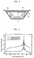
- FIG. 1 is a sectional view of a conventional lamp type LED device that is disclosed in U.S. Patent No. 6,069,440.
- a lamp type LED device 10 includes a mount lead 11 and an inner lead 12.
- An LED chip 14 is installed in a reflector cup 20 that is formed in the upper portion of the mount lead 11.
- the LED chip 14 has an n electrode and a p electrode which are electrically connected to the mount lead 11 and the inner lead 12, respectively, by a wire 15.
- the LED chip 14 is covered by a phosphor layer 16 that is a mixture of phosphor and transparent encapsulant. These constituent elements are surrounded by a seal substance 17.
- the reflector cup 20 is coated with silver (Ag) or aluminum (Al) for the high reflection of visible light rays.
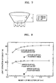
- FIGS. 2A, 2B, and 2C show various arrangements of the phosphor in the reflector cup 20.
- the LED chip 14 is arranged at the bottom of the reflector cup 20.
- Phosphors 22 are distributed in the transparent encapsulant 16 in the reflector cup 20.
- FIG. 2A shows the distribution of the phosphors 22 that are resolved in the transparent encapsulant (coating resin or polymer) 16 in the reflector cup 20.
- the LED chip 14 emits luminescence that excites the phosphors 22 to emit phosphorescence. Part of the phosphorescence collides against the surface of the LED chip 14 to be reabsorbed thereby. Thus, the luminous efficiency is lowered.
- FIG. 2B shows that the phosphors 22 are distributed on the surface of the LED chip 14. in this case, a probability that the phosphorescence of the phosphors 22 collides against the LED chip 14 increases so that the luminous efficiency is reduced.
- FIG. 2C shows that the phosphors 22 are separated from the LED chip 14. In this case, the probability that the phosphorescence directly collides against the LED chip 14 is relatively lowered.
- the present invention provides an LED device having a diffuse reflective surface which improves the luminous efficiency by lowering the probability that phosphorescence collides against the LED chip.
- an LED device having a diffuse reflective surface comprises an LED chip emitting light, a reflector cup having the LED chip arranged at a bottom surface thereof and having an angled surface which diffusely reflects the light, and a light conversion material provided in the reflector cup and converting the light emitted by the LED chip into visible light rays.
- the angled surface is processed to be rough.
- the amount of light reflected at the angled surface decreases as a reflection angle with respect to the perpendicular plane of the angled surface increases regardless of an incident angle of the light to the angled surface.
- the light conversion material is a phosphor that is excited by the light emitted from the LED chip to emit visible light rays.
- the phosphor forms a phosphor layer in an upper portion of the reflector cup to be separated from the LED chip.
- the phosphor is spatially separated from the LED chip by a length equal or greater than the maximum length of the LED chip.
- the phosphor can be a single phosphor material or a plurality of phosphor materials that form a plurality of visible color rays, and the phosphors are mixed with one another.
- the phosphor is a plurality of phosphors that form a plurality of visible color rays, and the phosphors are stacked in multiple layers.
- a convex portion is formed on an upper surface of the encapsulant material.
- the convex portion can have a hemispheric shape.
- the LED chip is formed of III-V group nitride-based semiconductor compounds.
- the LED chip 14 that is a light emitter is installed on the bottom surface of a reflector cup 40.
- the reflector cup 40 is filled with a light transmitting material 46.
- a light conversion material for receiving light and outputting visible light rays having a longer wavelength is formed in the upper portion of the reflector cup 40.
- the light conversion material may be a plurality of phosphors 22 emitting a plurality of visible color rays or quantum dots.
- the inner surface of the reflector cup 40 including an angled surface is a diffuse surface 40a that is processed to be rough to emit diffuse.
- the diffuse surface 40a may be a rough surface obtained by, for example, sand blasting a metal surface.
- the phosphors 22 form a phosphor layer which is separated a predetermined distance from the LED chip 14. Because the phosphor layer is spatially separated from the LED chip 14, the probability that the phosphorescence directly collides against the surface of the LED chip 14 is lowered.
- the phosphor layer can be formed by mixing the plurality of phosphors 22 that form a plurality of visible color rays.
- the phosphor layer may be a plurality of layers composed of a plurality of phosphors that form a plurality of visible color rays.
- the light transmitting material 46 can be made of a transparent material such as epoxy resin, silicon, or PMMA, capable of transmitting the light from the LED chip 14.
- the LED chip 14 is formed of III-V group nitride-based semiconductor compounds.
- Rays 1 and 3 are incident upon the angled surface of the reflector cup 40 at an angle and reflected as a diffuse light. At this time, only the part of the diffuse light collides against the LED chip 14 and most of the diffuse light is emitted to the outside. Thus, the probability that the phosphorescence is reflected and collides against the LED chip 14 is lowered.
- the intensity of the diffuse light is proportional to a cosine function as shown in the following formula according to the angle of a diffuse surface with respect to a vertical plane of a diffuse surface regardless of the incident angle to the diffuse surface.
- I r denotes the intensity of a reflected light
- ⁇ denotes the angle of the reflection from the perpendicular direction of the diffuse surface.
- the diffuse surface can be obtained by sand blasting the reflection surface of the reflector cup 40 or by spraying nano-sized Ag or Al.
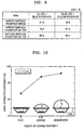
- FIG. 4 is a graph showing the relationship of light reflection on a specular mirror surface and a diffuse surface of the reflector cup.
- the specular mirror surface shows the intensity of the light at the reflective angle of 40° to be high as a level of about 10 4 .
- the light intensity at the reflective angle of 40° is a level of about 10 2 .
- the light intensity at the diffuse surface shows greater by 2 orders than that at the reflection surface.
- the sand-blastered reflective surface exhibits the characteristics of both diffuse surface and specular mirror surface.
- FIGS. 5A, 5B, 5C, and 5D show four cases in a ray tracing test for an LED device having a reflector cup with a diffuse surface according to an embodiment of the present invention and the conventional LED device having a reflector cup with a specular mirror surface.
- FIGS.5A and 5B show cases in which the phosphors 22 are distributed inside the reflector cup 40 while FIGS. 5C and 5D show cases in which the phosphors 22 form a layer at the top portion of the reflector cup 40.
- FIGS. 5A and 5C show the reflector cup 40 having a specular mirror surface 40b while FIGS. 5B and 5D show the reflector cup 40 having a diffuse surface 40a.
- FIG. 6 is a table showing the result of a ray tracing simulation.
- FIG. 7 is a view illustrating the sizes of the reflector cup 40 and the LED chip 14 used for the simulation of FIG. 6.
- a phosphor light source (not shown) having a wavelength of 550 nm is a cylinder type source having a thickness of 100 ⁇ m that is regularly distributed. Referring to FIGS.
- the refractive index n epoxy of the seal epoxy is 1.6
- the refractive index n phosphor of the phosphors 22 is 1.82
- the reflectance R Ag reflector of the surface of the reflector cup 40 is 95%
- the reflectance R LED chip of the LED chip 14 is 50%
- the thickness of the LED chip 14 is 100 ⁇ m
- the size of the LED chip 14 is 300 ⁇ m ⁇ 300 ⁇ m.
- the table of FIG. 6 is a light extraction efficiency according to the change in the length b from the LED chip 14 to the angled surface, the change in the height h of the reflector cup 40, and the angle ⁇ of the angled surface.
- FIG. 8 is a graph showing the light extraction efficiency according to the height of the reflector cup 40.
- “h” is 1 mm
- " ⁇ " is 45°
- "b” is 150 ⁇ m
- the light extraction efficiency in the case in which the phosphor is located at the top portion of the reflector cup 40 is higher than that of the case in which the phosphor is located inside the reflector cup 40.
- the light extraction efficiency of the reflector cup 40 having the diffuse surface is higher than that of the reflector cup having the specular mirror surface. This improvement in the light extraction efficiency results from the decrease in the probability of the re-absorption of light by the LED chip 14.
- FIG. 9 is a table showing the light conversion efficiency according to the types of the reflection surface and the positions of the phosphor at the reflector cup.
- the light conversion efficiency is a result of calculating the amount of a decrease in the light amount from the LED chip 14 as the light conversion amount in the phosphor.
- the light conversion efficiencies of the case in which the reflective surface is the specular mirror surface and the phosphor forms the top layer in the reflector cup 40 and the case in which the reflective surface is the diffuse surface and the phosphor forms the top layer in the reflector cup 40 are respectively 13.1 % and 27% higher than that of the case in which the reflective surface is a specular mirror surface and the phosphor is located inside the reflector cup 40.
- the light conversion efficiency is improved.
- FIG. 10 is a graph showing the change of the light extraction efficiency according to a convex portion which is formed on the reflector cup 40 with the diffuse surface. Referring to FIG. 10, the result of the ray tracing simulation shows that the light extraction efficiency increases when the surface of the reflector cup 40 is convex than flat.
- the light extraction efficiency can be easily improved by processing the reflective surface of the reflector cup to be rough. Also, the light extraction efficiency can be improved by arranging the phosphor at the top portion of the reflector cup. Thus, since the overall light conversion efficiency of the LED device is improved, the amount of output light is increased.
Abstract
Description
- The present invention relates to a light emitting diode (LED) device, and more particularly, to an LED device which employs a large spatial separation between a luminescence-generating semiconductor and a phosphorescence-generating light-conversion material and has a reflector cup having a diffuse reflective surface to diffusely reflect light, thus improving a luminous efficiency.
- Light emitting diode (LED) devices convert ultraviolet light rays or blue light rays emitted from an LED chip into visible light rays that have a longer wavelength. Recently, the LED device draws wide attention for its function of emitting white light or visible light rays of various colors. For example, in a white LED device, an ultraviolet ray emitted from the LED chip excites a phosphor. Then, the three primary colors of light, that is, red (R), green (G), and blue (B) visible rays, or yellow (Y) or blue (B) visible rays are emitted from the phosphor. The visible color rays emitted from the phosphor vary dependent on the composition of the phosphor. These visible rays combined with each other result in white light to the eyes of a human.
- FIG. 1 is a sectional view of a conventional lamp type LED device that is disclosed in U.S. Patent No. 6,069,440. Referring to FIG. 1, a lamp
type LED device 10 includes amount lead 11 and aninner lead 12. AnLED chip 14 is installed in areflector cup 20 that is formed in the upper portion of themount lead 11. TheLED chip 14 has an n electrode and a p electrode which are electrically connected to themount lead 11 and theinner lead 12, respectively, by awire 15. TheLED chip 14 is covered by aphosphor layer 16 that is a mixture of phosphor and transparent encapsulant. These constituent elements are surrounded by aseal substance 17. Thereflector cup 20 is coated with silver (Ag) or aluminum (Al) for the high reflection of visible light rays. - FIGS. 2A, 2B, and 2C show various arrangements of the phosphor in the
reflector cup 20. Referring to FIGS. 2A, 2B, and 2C, theLED chip 14 is arranged at the bottom of thereflector cup 20.Phosphors 22 are distributed in thetransparent encapsulant 16 in thereflector cup 20. - FIG. 2A shows the distribution of the
phosphors 22 that are resolved in the transparent encapsulant (coating resin or polymer) 16 in thereflector cup 20. TheLED chip 14 emits luminescence that excites thephosphors 22 to emit phosphorescence. Part of the phosphorescence collides against the surface of theLED chip 14 to be reabsorbed thereby. Thus, the luminous efficiency is lowered. - FIG. 2B shows that the
phosphors 22 are distributed on the surface of theLED chip 14. in this case, a probability that the phosphorescence of thephosphors 22 collides against theLED chip 14 increases so that the luminous efficiency is reduced. - FIG. 2C shows that the
phosphors 22 are separated from theLED chip 14. In this case, the probability that the phosphorescence directly collides against theLED chip 14 is relatively lowered. - To solve the above and/or other problems, the present invention provides an LED device having a diffuse reflective surface which improves the luminous efficiency by lowering the probability that phosphorescence collides against the LED chip.
- According to an aspect of the present invention, an LED device having a diffuse reflective surface comprises an LED chip emitting light, a reflector cup having the LED chip arranged at a bottom surface thereof and having an angled surface which diffusely reflects the light, and a light conversion material provided in the reflector cup and converting the light emitted by the LED chip into visible light rays.
- The angled surface is processed to be rough. The amount of light reflected at the angled surface decreases as a reflection angle with respect to the perpendicular plane of the angled surface increases regardless of an incident angle of the light to the angled surface. The light conversion material is a phosphor that is excited by the light emitted from the LED chip to emit visible light rays.
- The phosphor forms a phosphor layer in an upper portion of the reflector cup to be separated from the LED chip. The phosphor is spatially separated from the LED chip by a length equal or greater than the maximum length of the LED chip. The phosphor can be a single phosphor material or a plurality of phosphor materials that form a plurality of visible color rays, and the phosphors are mixed with one another.
- The phosphor is a plurality of phosphors that form a plurality of visible color rays, and the phosphors are stacked in multiple layers. A convex portion is formed on an upper surface of the encapsulant material. The convex portion can have a hemispheric shape. The LED chip is formed of III-V group nitride-based semiconductor compounds.
- The above and other features and advantages of the present invention will become more apparent by describing in detail preferred embodiments thereof with reference to the attached drawings in which:
- FIG. 1 is a sectional view of the conventional lamp type LED device;
- FIGS. 2A, 2B, and 2C are sectional views showing the arrangements of phosphor in the reflector cup, especially FIG. 2C shows the principle of the present invention.
- FIG. 3 is a view for explaining the principle of the present invention;
- FIG. 4 is a graph showing the relationship of light reflection on a specular mirror surface and a diffuse surface of the reflector cup;
- FIGS. 5A, 5B, 5C, and 5D show four cases in a ray tracing test for an LED device having a reflector chip with a diffuse surface according to an embodiment of the present invention and the conventional LED device having a reflector cup with a specular mirror surface;
- FIG. 6 is a table showing the result of a ray tracing simulation;
- FIG. 7 is a view illustrating the sizes of the reflector cup and the LED chip used for the simulation of FIG. 6;
- FIG. 8 is a graph showing the light extraction efficiency according to the height of the reflector cup;
- FIG. 9 is a table showing the light conversion efficiency according to the types of the reflection surface and the positions of the phosphor of the reflector cup; and
- FIG. 10 is a graph showing the change of the light extraction efficiency according to a convex portion which is formed on the reflector cup with the diffuse surface.
- Referring to FIG. 3, the
LED chip 14 that is a light emitter is installed on the bottom surface of areflector cup 40. Thereflector cup 40 is filled with alight transmitting material 46. A light conversion material for receiving light and outputting visible light rays having a longer wavelength is formed in the upper portion of thereflector cup 40. The light conversion material may be a plurality ofphosphors 22 emitting a plurality of visible color rays or quantum dots. The inner surface of thereflector cup 40 including an angled surface is a diffusesurface 40a that is processed to be rough to emit diffuse. The diffusesurface 40a may be a rough surface obtained by, for example, sand blasting a metal surface. Thephosphors 22 form a phosphor layer which is separated a predetermined distance from theLED chip 14. Because the phosphor layer is spatially separated from theLED chip 14, the probability that the phosphorescence directly collides against the surface of theLED chip 14 is lowered. - The phosphor layer can be formed by mixing the plurality of
phosphors 22 that form a plurality of visible color rays. Alternatively, the phosphor layer may be a plurality of layers composed of a plurality of phosphors that form a plurality of visible color rays. Thelight transmitting material 46 can be made of a transparent material such as epoxy resin, silicon, or PMMA, capable of transmitting the light from theLED chip 14. - The
LED chip 14 is formed of III-V group nitride-based semiconductor compounds. Aray 2 of the phosphorescence that thephosphors 22 having received the light from theLED chip 14 emit collides against the surface of theLED chip 14 so that 50% of theray 2 is absorbed by theLED chip 14.Rays reflector cup 40 at an angle and reflected as a diffuse light. At this time, only the part of the diffuse light collides against theLED chip 14 and most of the diffuse light is emitted to the outside. Thus, the probability that the phosphorescence is reflected and collides against theLED chip 14 is lowered. - The intensity of the diffuse light is proportional to a cosine function as shown in the following formula according to the angle of a diffuse surface with respect to a vertical plane of a diffuse surface regardless of the incident angle to the diffuse surface.

- Here, Ir denotes the intensity of a reflected light and θ denotes the angle of the reflection from the perpendicular direction of the diffuse surface. The diffuse surface can be obtained by sand blasting the reflection surface of the
reflector cup 40 or by spraying nano-sized Ag or Al. - FIG. 4 is a graph showing the relationship of light reflection on a specular mirror surface and a diffuse surface of the reflector cup. Referring to FIG. 4, when the incident angle of light at a silver (Ag) coated reflective surface is 40°, the specular mirror surface shows the intensity of the light at the reflective angle of 40° to be high as a level of about 104. However, for the sand-blastered diffuse surface, the light intensity at the reflective angle of 40° is a level of about 102. At a different angle, the light intensity at the diffuse surface shows greater by 2 orders than that at the reflection surface. Thus, the sand-blastered reflective surface exhibits the characteristics of both diffuse surface and specular mirror surface.
- FIGS. 5A, 5B, 5C, and 5D show four cases in a ray tracing test for an LED device having a reflector cup with a diffuse surface according to an embodiment of the present invention and the conventional LED device having a reflector cup with a specular mirror surface. FIGS.5A and 5B show cases in which the
phosphors 22 are distributed inside thereflector cup 40 while FIGS. 5C and 5D show cases in which thephosphors 22 form a layer at the top portion of thereflector cup 40. FIGS. 5A and 5C show thereflector cup 40 having aspecular mirror surface 40b while FIGS. 5B and 5D show thereflector cup 40 having a diffusesurface 40a. - FIG. 6 is a table showing the result of a ray tracing simulation. FIG. 7 is a view illustrating the sizes of the
reflector cup 40 and theLED chip 14 used for the simulation of FIG. 6. Here, a phosphor light source (not shown) having a wavelength of 550 nm is a cylinder type source having a thickness of 100 µm that is regularly distributed. Referring to FIGS. 6 and 7, the refractive index nepoxy of the seal epoxy is 1.6, the refractive index nphosphor of thephosphors 22 is 1.82, the reflectance RAg reflector of the surface of thereflector cup 40 is 95%, the reflectance RLED chip of theLED chip 14 is 50%, the thickness of theLED chip 14 is 100 µm, and the size of theLED chip 14 is 300 µm×300 µm. The table of FIG. 6 is a light extraction efficiency according to the change in the length b from theLED chip 14 to the angled surface, the change in the height h of thereflector cup 40, and the angle θ of the angled surface. - FIG. 8 is a graph showing the light extraction efficiency according to the height of the
reflector cup 40. Referring to FIG. 6 and 8, when "h" is 1 mm, "θ" is 45°, and "b" is 150 µm, it is noted that the light extraction efficiency in the case in which the phosphor is located at the top portion of thereflector cup 40 is higher than that of the case in which the phosphor is located inside thereflector cup 40. Also, the light extraction efficiency of thereflector cup 40 having the diffuse surface is higher than that of the reflector cup having the specular mirror surface. This improvement in the light extraction efficiency results from the decrease in the probability of the re-absorption of light by theLED chip 14. - FIG. 9 is a table showing the light conversion efficiency according to the types of the reflection surface and the positions of the phosphor at the reflector cup. The light conversion efficiency is a result of calculating the amount of a decrease in the light amount from the
LED chip 14 as the light conversion amount in the phosphor. - Referring to 9, when a blue phosphor is excited by an UV LED, the light conversion efficiencies of the case in which the reflective surface is the specular mirror surface and the phosphor forms the top layer in the
reflector cup 40 and the case in which the reflective surface is the diffuse surface and the phosphor forms the top layer in thereflector cup 40 are respectively 13.1 % and 27% higher than that of the case in which the reflective surface is a specular mirror surface and the phosphor is located inside thereflector cup 40. In the case in which a blue LED excites the yellow phosphor, when the reflective surface is the diffuse surface and the phosphor forms the top layer in thereflector cup 40, the light conversion efficiency is improved. - FIG. 10 is a graph showing the change of the light extraction efficiency according to a convex portion which is formed on the
reflector cup 40 with the diffuse surface. Referring to FIG. 10, the result of the ray tracing simulation shows that the light extraction efficiency increases when the surface of thereflector cup 40 is convex than flat. - As described above, according to the LED device according to the present invention, the light extraction efficiency can be easily improved by processing the reflective surface of the reflector cup to be rough. Also, the light extraction efficiency can be improved by arranging the phosphor at the top portion of the reflector cup. Thus, since the overall light conversion efficiency of the LED device is improved, the amount of output light is increased.
- While this invention has been particularly shown and described with reference to preferred embodiments thereof, it will be understood by those skilled in the art that various changes in form and details may be made therein without departing from the scope of the invention as defined by the appended claims.
Claims (14)
- An LED device having a diffuse reflective surface, the LED device comprising:an LED chip emitting light:a reflector cup having the LED chip arranged at a bottom surface thereof and having an angled surface which diffusely reflects light; anda light conversion material provided in the reflector cup and converting the light emitted by the LED chip into visible light.
- The LED device as claimed in claim1, wherein the angled surface is processed to be rough.
- The LED device as claimed in claim 2, wherein the amount of light reflected at the angled surface decreases as a reflection angle with respect to a perpendicular direction to the angled surface increases regardless of an incident angle of the light to the angled surface.
- The LED device as claimed in any preceding claim, wherein the light conversion material is a phosphor that is excited by the light emitted from the LED chip to emit visible light.
- The LED device as claimed in claim 4, wherein the phosphor forms a phosphor layer in an upper portion of the reflector cup separated from the LED chip.
- The LED device as claimed in claim 5, wherein the phosphor is separated by a distance equal or greater than the maximum length of the LED chip from the LED chip.
- The LED device as claimed in claim 5 or 6, wherein the phosphor is a plurality of phosphors that form a plurality of visible color rays, and the phosphors are mixed with one another.
- The LED device as claimed in claim 5, 6 or 7, wherein the phosphor is a plurality of phosphors that form a plurality of visible color rays, and the phosphors are stacked in multiple layers.
- The LED device as claimed in claim 5, 6, 7 or 8, wherein a convex portion is formed on an upper surface of the phosphor layer.
- The LED device as claimed in claim 9, wherein the convex portion has a hemispheric shape.
- The LED device as claimed in any preceding claim, wherein the LED chip is formed of III-V group nitride-based semiconductor compounds.
- An LED device, the LED device comprising:an LED chip emitting light:a reflector cup having the LED chip arranged at a bottom surface thereof and having an angled surface which reflects light; anda light conversion material provided in the reflector cup and converting the light emitted by the LED chip into visible light,wherein the light conversion material is separated over the LED chip.
- The LED device as claimed in claim 12, wherein the light conversion material is a phosphor that is excited by the light emitted from the LED chip to emit visible light.
- The LED device as claimed in claim 13, wherein the phosphor is separated by a distance equal or greater than the maximum length of the LED chip from the LED chip.
Applications Claiming Priority (2)
| Application Number | Priority Date | Filing Date | Title |
|---|---|---|---|
| US64849405P | 2005-01-31 | 2005-01-31 | |
| KR1020050040164A KR101139891B1 (en) | 2005-01-31 | 2005-05-13 | Light emitting diode device having diffusedly reflective surface |
Publications (2)
| Publication Number | Publication Date |
|---|---|
| EP1686630A2 true EP1686630A2 (en) | 2006-08-02 |
| EP1686630A3 EP1686630A3 (en) | 2009-03-04 |
Family
ID=36177972
Family Applications (1)
| Application Number | Title | Priority Date | Filing Date |
|---|---|---|---|
| EP20050257882 Withdrawn EP1686630A3 (en) | 2005-01-31 | 2005-12-20 | Led device having diffuse reflective surface |
Country Status (2)
| Country | Link |
|---|---|
| EP (1) | EP1686630A3 (en) |
| JP (1) | JP2006216953A (en) |
Cited By (25)
| Publication number | Priority date | Publication date | Assignee | Title |
|---|---|---|---|---|
| WO2008027093A2 (en) * | 2006-08-31 | 2008-03-06 | Rensselaer Polytechnic Institute | High-efficiency light- emitting apparatus using light emitting diodes |
| EP1965122A1 (en) * | 2007-02-06 | 2008-09-03 | Ningbo Andy Optoelectronic Co., Ltd. | High power light emitting diode (LED) illumination apparatus |
| NL2002149C (en) * | 2008-10-29 | 2010-05-03 | Lightronics B V | FOR MOUNTING IN A STREET LIGHTING LUMINAIRE FITTED WITH LED'S LIGHTING UNIT. |
| US7750359B2 (en) | 2005-06-23 | 2010-07-06 | Rensselaer Polytechnic Institute | Package design for producing white light with short-wavelength LEDS and down-conversion materials |
| CN101834263A (en) * | 2010-04-27 | 2010-09-15 | 南京吉山光电科技有限公司 | Integrated light source structure with wide-angle transmission |
| EP2237331A1 (en) * | 2007-12-26 | 2010-10-06 | Kyocera Corporation | Light-emitting device and illuminating device |
| US7819549B2 (en) | 2004-05-05 | 2010-10-26 | Rensselaer Polytechnic Institute | High efficiency light source using solid-state emitter and down-conversion material |
| US7837348B2 (en) | 2004-05-05 | 2010-11-23 | Rensselaer Polytechnic Institute | Lighting system using multiple colored light emitting sources and diffuser element |
| US7889421B2 (en) | 2006-11-17 | 2011-02-15 | Rensselaer Polytechnic Institute | High-power white LEDs and manufacturing method thereof |
| WO2011127909A1 (en) * | 2010-04-15 | 2011-10-20 | Excelitas Technologies Elcos Gmbh | Liquid reflector |
| WO2012120434A1 (en) | 2011-03-07 | 2012-09-13 | Koninklijke Philips Electronics N.V. | A light emitting module, a lamp, a luminaire and a display device |
| WO2012120332A1 (en) * | 2011-03-07 | 2012-09-13 | Koninklijke Philips Electronics N.V. | A light emitting module, a lamp and a luminaire |
| WO2012135976A1 (en) * | 2011-04-07 | 2012-10-11 | Cree Huizhou Solid State Lighting Company Limited | Led device having tilted peak emission and led display including such devices |
| WO2013041979A1 (en) * | 2011-09-20 | 2013-03-28 | Koninklijke Philips Electronics N.V. | A light emitting module, a lamp, a luminaire and a display device |
| CN103109385A (en) * | 2010-07-20 | 2013-05-15 | 金钟律 | LED package and method for manufacturing LED package |
| US8487326B2 (en) | 2006-04-24 | 2013-07-16 | Cree, Inc. | LED device having a tilted peak emission and an LED display including such devices |
| CN103459919A (en) * | 2008-08-14 | 2013-12-18 | 库帕技术公司 | Led devices for offset wide beam generation |
| EP2176895A4 (en) * | 2007-07-25 | 2015-07-15 | Lg Innotek Co Ltd | Light emitting device package and method of manufacturing the same |
| US9140430B2 (en) | 2011-02-28 | 2015-09-22 | Cooper Technologies Company | Method and system for managing light from a light emitting diode |
| US9200765B1 (en) | 2012-11-20 | 2015-12-01 | Cooper Technologies Company | Method and system for redirecting light emitted from a light emitting diode |
| US9388949B2 (en) | 2006-02-27 | 2016-07-12 | Illumination Management Solutions, Inc. | LED device for wide beam generation |
| US9435510B2 (en) | 2011-02-28 | 2016-09-06 | Cooper Technologies Company | Method and system for managing light from a light emitting diode |
| US10174908B2 (en) | 2006-02-27 | 2019-01-08 | Eaton Intelligent Power Limited | LED device for wide beam generation |
| CN110680937A (en) * | 2019-11-08 | 2020-01-14 | 中国科学院半导体研究所 | Ultraviolet LED light uniformizing device and application thereof |
| US11210971B2 (en) | 2009-07-06 | 2021-12-28 | Cree Huizhou Solid State Lighting Company Limited | Light emitting diode display with tilted peak emission pattern |
Families Citing this family (4)
| Publication number | Priority date | Publication date | Assignee | Title |
|---|---|---|---|---|
| US7910938B2 (en) | 2006-09-01 | 2011-03-22 | Cree, Inc. | Encapsulant profile for light emitting diodes |
| EP2158427A4 (en) * | 2007-05-21 | 2013-04-03 | Light Engine Ltd | Led luminance-augmentation via specular retroreflection, including collimators that escape the etendue limit |
| JP5507372B2 (en) * | 2010-07-22 | 2014-05-28 | スタンレー電気株式会社 | Light emitting device |
| JP6024685B2 (en) * | 2014-03-06 | 2016-11-16 | 日亜化学工業株式会社 | Light emitting device |
Citations (1)
| Publication number | Priority date | Publication date | Assignee | Title |
|---|---|---|---|---|
| US6069440A (en) | 1996-07-29 | 2000-05-30 | Nichia Kagaku Kogyo Kabushiki Kaisha | Light emitting device having a nitride compound semiconductor and a phosphor containing a garnet fluorescent material |
Family Cites Families (11)
| Publication number | Priority date | Publication date | Assignee | Title |
|---|---|---|---|---|
| JPS6054354U (en) * | 1983-09-21 | 1985-04-16 | 鹿児島日本電気株式会社 | light emitting diode device |
| JP3704941B2 (en) * | 1998-03-30 | 2005-10-12 | 日亜化学工業株式会社 | Light emitting device |
| US6429583B1 (en) * | 1998-11-30 | 2002-08-06 | General Electric Company | Light emitting device with ba2mgsi2o7:eu2+, ba2sio4:eu2+, or (srxcay ba1-x-y)(a1zga1-z)2sr:eu2+phosphors |
| JP2003282955A (en) * | 2001-07-19 | 2003-10-03 | Rohm Co Ltd | Semiconductor light-emitting device having reflector case |
| TW552726B (en) * | 2001-07-26 | 2003-09-11 | Matsushita Electric Works Ltd | Light emitting device in use of LED |
| JP3939177B2 (en) * | 2002-03-20 | 2007-07-04 | シャープ株式会社 | Method for manufacturing light emitting device |
| JP3707688B2 (en) * | 2002-05-31 | 2005-10-19 | スタンレー電気株式会社 | Light emitting device and manufacturing method thereof |
| JP3843245B2 (en) * | 2002-06-26 | 2006-11-08 | 宣彦 澤木 | Semiconductor light emitting element and semiconductor light emitting device |
| CN100468791C (en) * | 2002-08-30 | 2009-03-11 | 吉尔科有限公司 | Light emitting diode with improved effience |
| JP3717480B2 (en) * | 2003-01-27 | 2005-11-16 | ローム株式会社 | Semiconductor light emitting device |
| JPWO2004097294A1 (en) * | 2003-05-02 | 2006-07-13 | 株式会社アベイラス | Light emitting face structure |
-
2005
- 2005-12-20 EP EP20050257882 patent/EP1686630A3/en not_active Withdrawn
-
2006
- 2006-01-31 JP JP2006023877A patent/JP2006216953A/en active Pending
Patent Citations (1)
| Publication number | Priority date | Publication date | Assignee | Title |
|---|---|---|---|---|
| US6069440A (en) | 1996-07-29 | 2000-05-30 | Nichia Kagaku Kogyo Kabushiki Kaisha | Light emitting device having a nitride compound semiconductor and a phosphor containing a garnet fluorescent material |
Non-Patent Citations (1)
| Title |
|---|
| "Technical Guide Reflectance Materials and Coatings", 16 March 2015 (2015-03-16), pages 1 - 26, XP055187716, Retrieved from the Internet <URL:http://www.labsphere.com/uploads/technical-guides/a-guide-to-reflectance-materials-and-coatings.pdf> [retrieved on 20150506] * |
Cited By (54)
| Publication number | Priority date | Publication date | Assignee | Title |
|---|---|---|---|---|
| US8960953B2 (en) | 2004-05-05 | 2015-02-24 | Rensselaer Polytechnic Institute | Lighting source using solid state emitter and phosphor materials |
| US11028979B2 (en) | 2004-05-05 | 2021-06-08 | Rensselaer Polytechnic Institute | Lighting source using solid state emitter and phosphor materials |
| US8764225B2 (en) | 2004-05-05 | 2014-07-01 | Rensselaer Polytechnic Institute | Lighting source using solid state emitter and phosphor materials |
| US9447945B2 (en) | 2004-05-05 | 2016-09-20 | Rensselaer Polytechnic Institute | Lighting source using solid state emitter and phosphor materials |
| US7819549B2 (en) | 2004-05-05 | 2010-10-26 | Rensselaer Polytechnic Institute | High efficiency light source using solid-state emitter and down-conversion material |
| US7837348B2 (en) | 2004-05-05 | 2010-11-23 | Rensselaer Polytechnic Institute | Lighting system using multiple colored light emitting sources and diffuser element |
| US7750359B2 (en) | 2005-06-23 | 2010-07-06 | Rensselaer Polytechnic Institute | Package design for producing white light with short-wavelength LEDS and down-conversion materials |
| US10174908B2 (en) | 2006-02-27 | 2019-01-08 | Eaton Intelligent Power Limited | LED device for wide beam generation |
| US9388949B2 (en) | 2006-02-27 | 2016-07-12 | Illumination Management Solutions, Inc. | LED device for wide beam generation |
| US8487326B2 (en) | 2006-04-24 | 2013-07-16 | Cree, Inc. | LED device having a tilted peak emission and an LED display including such devices |
| WO2008027093A2 (en) * | 2006-08-31 | 2008-03-06 | Rensselaer Polytechnic Institute | High-efficiency light- emitting apparatus using light emitting diodes |
| US7703942B2 (en) | 2006-08-31 | 2010-04-27 | Rensselaer Polytechnic Institute | High-efficient light engines using light emitting diodes |
| WO2008027093A3 (en) * | 2006-08-31 | 2008-04-24 | Rensselaer Polytech Inst | High-efficiency light- emitting apparatus using light emitting diodes |
| US8031393B2 (en) | 2006-11-17 | 2011-10-04 | Renesselaer Polytechnic Institute | High-power white LEDs and manufacturing method thereof |
| US7889421B2 (en) | 2006-11-17 | 2011-02-15 | Rensselaer Polytechnic Institute | High-power white LEDs and manufacturing method thereof |
| US8164825B2 (en) | 2006-11-17 | 2012-04-24 | Rensselaer Polytechnic Institute | High-power white LEDs and manufacturing method thereof |
| US9105816B2 (en) | 2006-11-17 | 2015-08-11 | Rensselaer Polytechnic Institute | High-power white LEDs |
| US10305001B2 (en) | 2006-11-17 | 2019-05-28 | Rensselaer Polytechnic Institute | High-power white LEDs |
| EP1965122A1 (en) * | 2007-02-06 | 2008-09-03 | Ningbo Andy Optoelectronic Co., Ltd. | High power light emitting diode (LED) illumination apparatus |
| EP2176895A4 (en) * | 2007-07-25 | 2015-07-15 | Lg Innotek Co Ltd | Light emitting device package and method of manufacturing the same |
| US9287466B2 (en) | 2007-07-25 | 2016-03-15 | Lg Innotek Co., Ltd. | Light emitting device package and method of manufacturing the same |
| EP2237331A4 (en) * | 2007-12-26 | 2013-05-01 | Kyocera Corp | Light-emitting device and illuminating device |
| US8529089B2 (en) | 2007-12-26 | 2013-09-10 | Kyocera Corporation | Light emitting device and illumination device |
| EP2237331A1 (en) * | 2007-12-26 | 2010-10-06 | Kyocera Corporation | Light-emitting device and illuminating device |
| US10400996B2 (en) | 2008-08-14 | 2019-09-03 | Eaton Intelligent Power Limited | LED devices for offset wide beam generation |
| EP2326870B1 (en) * | 2008-08-14 | 2017-01-25 | Cooper Technologies Company | Led devices for offset wide beam generation |
| CN103459919A (en) * | 2008-08-14 | 2013-12-18 | 库帕技术公司 | Led devices for offset wide beam generation |
| US10222030B2 (en) | 2008-08-14 | 2019-03-05 | Cooper Technologies Company | LED devices for offset wide beam generation |
| US10976027B2 (en) | 2008-08-14 | 2021-04-13 | Signify Holding B.V. | LED devices for offset wide beam generation |
| US9297517B2 (en) | 2008-08-14 | 2016-03-29 | Cooper Technologies Company | LED devices for offset wide beam generation |
| NL2002149C (en) * | 2008-10-29 | 2010-05-03 | Lightronics B V | FOR MOUNTING IN A STREET LIGHTING LUMINAIRE FITTED WITH LED'S LIGHTING UNIT. |
| US11210971B2 (en) | 2009-07-06 | 2021-12-28 | Cree Huizhou Solid State Lighting Company Limited | Light emitting diode display with tilted peak emission pattern |
| WO2011127909A1 (en) * | 2010-04-15 | 2011-10-20 | Excelitas Technologies Elcos Gmbh | Liquid reflector |
| CN101834263A (en) * | 2010-04-27 | 2010-09-15 | 南京吉山光电科技有限公司 | Integrated light source structure with wide-angle transmission |
| CN103109385A (en) * | 2010-07-20 | 2013-05-15 | 金钟律 | LED package and method for manufacturing LED package |
| US9574746B2 (en) | 2011-02-28 | 2017-02-21 | Cooper Technologies Company | Method and system for managing light from a light emitting diode |
| US9435510B2 (en) | 2011-02-28 | 2016-09-06 | Cooper Technologies Company | Method and system for managing light from a light emitting diode |
| US9458983B2 (en) | 2011-02-28 | 2016-10-04 | Cooper Technologies Company | Method and system for managing light from a light emitting diode |
| US9140430B2 (en) | 2011-02-28 | 2015-09-22 | Cooper Technologies Company | Method and system for managing light from a light emitting diode |
| RU2581426C2 (en) * | 2011-03-07 | 2016-04-20 | Конинклейке Филипс Н.В. | Light-emitting module, lamp, lighting device and display device |
| US9082946B2 (en) | 2011-03-07 | 2015-07-14 | Koninklijke Philips N.V. | Light emitting module, a lamp, a luminaire and a display device |
| JP2014515863A (en) * | 2011-03-07 | 2014-07-03 | コーニンクレッカ フィリップス エヌ ヴェ | Light emitting module, lamp, lighting fixture, and display device |
| CN103403894B (en) * | 2011-03-07 | 2016-10-26 | 皇家飞利浦有限公司 | Light emitting module, lamp, illumination apparatus and display device |
| WO2012120434A1 (en) | 2011-03-07 | 2012-09-13 | Koninklijke Philips Electronics N.V. | A light emitting module, a lamp, a luminaire and a display device |
| WO2012120332A1 (en) * | 2011-03-07 | 2012-09-13 | Koninklijke Philips Electronics N.V. | A light emitting module, a lamp and a luminaire |
| CN103403894A (en) * | 2011-03-07 | 2013-11-20 | 皇家飞利浦有限公司 | A light emitting module, a lamp, a luminaire and a display device |
| WO2012135976A1 (en) * | 2011-04-07 | 2012-10-11 | Cree Huizhou Solid State Lighting Company Limited | Led device having tilted peak emission and led display including such devices |
| US9599292B2 (en) | 2011-09-20 | 2017-03-21 | Koninklijke Philips N.V. | Light emitting module, a lamp, a luminaire and a display device |
| WO2013041979A1 (en) * | 2011-09-20 | 2013-03-28 | Koninklijke Philips Electronics N.V. | A light emitting module, a lamp, a luminaire and a display device |
| CN103797597B (en) * | 2011-09-20 | 2017-08-15 | 皇家飞利浦有限公司 | Light emitting module, lamp, luminaire and display device |
| RU2586385C2 (en) * | 2011-09-20 | 2016-06-10 | Конинклейке Филипс Н.В. | Light-emitting module, lamp, lighting device and display device |
| CN103797597A (en) * | 2011-09-20 | 2014-05-14 | 皇家飞利浦有限公司 | A light emitting module, a lamp, a luminaire and a display device |
| US9200765B1 (en) | 2012-11-20 | 2015-12-01 | Cooper Technologies Company | Method and system for redirecting light emitted from a light emitting diode |
| CN110680937A (en) * | 2019-11-08 | 2020-01-14 | 中国科学院半导体研究所 | Ultraviolet LED light uniformizing device and application thereof |
Also Published As
| Publication number | Publication date |
|---|---|
| JP2006216953A (en) | 2006-08-17 |
| EP1686630A3 (en) | 2009-03-04 |
Similar Documents
| Publication | Publication Date | Title |
|---|---|---|
| EP1686630A2 (en) | Led device having diffuse reflective surface | |
| US7816855B2 (en) | LED device having diffuse reflective surface | |
| US9882097B2 (en) | Optoelectronic semiconductor chip, optoelectronic semiconductor component, and a method for producing an optoelectronic semiconductor component | |
| US10050022B2 (en) | Optoelectronic component | |
| KR100944008B1 (en) | White light emitting diode and fabrication method thereof | |
| EP1381091B1 (en) | Light emitting diode | |
| US8039850B2 (en) | White light emitting device | |
| US7503676B2 (en) | Light-emitting device and illuminating apparatus | |
| EP3276681B1 (en) | Light emitting device and the manufacturing method for same | |
| TWI766032B (en) | Light-emitting device and method of manufacturing same | |
| EP1480278A2 (en) | Light emitting diode comprising a fluorescent multilayer | |
| US20150129902A1 (en) | Lighting device | |
| CN104885235B (en) | For the LED of the growth substrates with forming of side transmitting | |
| TW201535797A (en) | Light emitting device | |
| JP2013232681A (en) | Semiconductor light-emitting device | |
| JP2005302920A (en) | Light emitting device | |
| JP2018107418A (en) | Light-emitting device | |
| JP2003243724A (en) | Light emitting apparatus | |
| TWI829671B (en) | Light-emitting device | |
| CN111509113B (en) | LED packaging structure, light emitting method thereof and light emitting device | |
| US20080211388A1 (en) | Light emitting semiconductor device | |
| JP4709405B2 (en) | Light emitting diode | |
| JP5678462B2 (en) | Light emitting device | |
| US20220052232A1 (en) | Light-altering particle arrangements for light-emitting devices | |
| JP7071652B2 (en) | Light emitting device and its manufacturing method |
Legal Events
| Date | Code | Title | Description |
|---|---|---|---|
| PUAI | Public reference made under article 153(3) epc to a published international application that has entered the european phase |
Free format text: ORIGINAL CODE: 0009012 |
|
| AK | Designated contracting states |
Kind code of ref document: A2 Designated state(s): AT BE BG CH CY CZ DE DK EE ES FI FR GB GR HU IE IS IT LI LT LU LV MC NL PL PT RO SE SI SK TR |
|
| AX | Request for extension of the european patent |
Extension state: AL BA HR MK YU |
|
| PUAL | Search report despatched |
Free format text: ORIGINAL CODE: 0009013 |
|
| AK | Designated contracting states |
Kind code of ref document: A3 Designated state(s): AT BE BG CH CY CZ DE DK EE ES FI FR GB GR HU IE IS IT LI LT LU LV MC NL PL PT RO SE SI SK TR |
|
| AX | Request for extension of the european patent |
Extension state: AL BA HR MK YU |
|
| 17P | Request for examination filed |
Effective date: 20090708 |
|
| 17Q | First examination report despatched |
Effective date: 20090812 |
|
| AKX | Designation fees paid |
Designated state(s): DE FR GB |
|
| RAP1 | Party data changed (applicant data changed or rights of an application transferred) |
Owner name: RENSSELAER POLYTECHNIC INSTITUTE Owner name: SAMSUNG LED CO., LTD. |
|
| RAP1 | Party data changed (applicant data changed or rights of an application transferred) |
Owner name: SAMSUNG ELECTRONICS CO., LTD. Owner name: RENSSELAER POLYTECHNIC INSTITUTE |
|
| STAA | Information on the status of an ep patent application or granted ep patent |
Free format text: STATUS: THE APPLICATION IS DEEMED TO BE WITHDRAWN |
|
| 18D | Application deemed to be withdrawn |
Effective date: 20170701 |