EP1648086A1 - Integrated circuit for controlling semiconductor power switches - Google Patents
Integrated circuit for controlling semiconductor power switches Download PDFInfo
- Publication number
- EP1648086A1 EP1648086A1 EP05017562A EP05017562A EP1648086A1 EP 1648086 A1 EP1648086 A1 EP 1648086A1 EP 05017562 A EP05017562 A EP 05017562A EP 05017562 A EP05017562 A EP 05017562A EP 1648086 A1 EP1648086 A1 EP 1648086A1
- Authority
- EP
- European Patent Office
- Prior art keywords
- circuit arrangement
- drive chip
- switch
- level shifter
- drive
- Prior art date
- Legal status (The legal status is an assumption and is not a legal conclusion. Google has not performed a legal analysis and makes no representation as to the accuracy of the status listed.)
- Withdrawn
Links
Images

Classifications
-
- H—ELECTRICITY
- H01—ELECTRIC ELEMENTS
- H01L—SEMICONDUCTOR DEVICES NOT COVERED BY CLASS H10
- H01L27/00—Devices consisting of a plurality of semiconductor or other solid-state components formed in or on a common substrate
- H01L27/02—Devices consisting of a plurality of semiconductor or other solid-state components formed in or on a common substrate including semiconductor components specially adapted for rectifying, oscillating, amplifying or switching and having at least one potential-jump barrier or surface barrier; including integrated passive circuit elements with at least one potential-jump barrier or surface barrier
- H01L27/04—Devices consisting of a plurality of semiconductor or other solid-state components formed in or on a common substrate including semiconductor components specially adapted for rectifying, oscillating, amplifying or switching and having at least one potential-jump barrier or surface barrier; including integrated passive circuit elements with at least one potential-jump barrier or surface barrier the substrate being a semiconductor body
-
- H—ELECTRICITY
- H03—ELECTRONIC CIRCUITRY
- H03K—PULSE TECHNIQUE
- H03K17/00—Electronic switching or gating, i.e. not by contact-making and –breaking
- H03K17/06—Modifications for ensuring a fully conducting state
- H03K17/063—Modifications for ensuring a fully conducting state in field-effect transistor switches
-
- H—ELECTRICITY
- H03—ELECTRONIC CIRCUITRY
- H03K—PULSE TECHNIQUE
- H03K17/00—Electronic switching or gating, i.e. not by contact-making and –breaking
- H03K17/10—Modifications for increasing the maximum permissible switched voltage
- H03K17/102—Modifications for increasing the maximum permissible switched voltage in field-effect transistor switches
-
- H—ELECTRICITY
- H01—ELECTRIC ELEMENTS
- H01L—SEMICONDUCTOR DEVICES NOT COVERED BY CLASS H10
- H01L2924/00—Indexing scheme for arrangements or methods for connecting or disconnecting semiconductor or solid-state bodies as covered by H01L24/00
- H01L2924/0001—Technical content checked by a classifier
- H01L2924/0002—Not covered by any one of groups H01L24/00, H01L24/00 and H01L2224/00
Definitions
- An integrated circuit arrangement is presented for controlling power semiconductor switches arranged as a single switch or in a bridge circuit.
- Such bridge arrangements of circuit breakers are known as one, two, or three-phase half-bridge circuits or as H-bridge circuits, wherein the single-phase half-bridge represents a basic building block of power electronic circuits.
- a half-bridge circuit two power switches, a first, so-called. TOP switch and a second so-called. BOT switch are arranged in a series circuit.
- Such a half-bridge usually has a connection to a DC intermediate circuit. The center tap is typically associated with a load.
- a drive circuit is necessary for driving the power switch.
- these drive circuits consist of a plurality of subcircuits or function blocks according to the prior art.
- the control signal coming from a higher-level control is processed in a first sub-circuit, the control logic, and supplied via further components to the driver circuits and finally to the control input of the respective circuit breaker.
- the control logic for the preparation of the control signals in terms of potential / galvanically separated from the driver circuits, since the associated circuit breakers are at different potential and thus a voltage isolation is inevitable.
- This separation takes place according to the prior art by way of example by means of transformers, Optocouplers or optical waveguides.
- This galvanic isolation applies at least to the TOP switch, but is also carried out at higher powers for the BOT switch due to a possible distortion of the ground potential during switching.
- the invention has for its object to provide an integrated circuit arrangement that uses known manufacturing technologies and can be used for higher voltage classes than is usual with these manufacturing technologies and at the same time suitable for use at higher operating temperatures above 125 ° C.
- the integrated circuit arrangement according to the invention serves to control power semiconductor switches arranged as individual switches or in a bridge circuit.
- the bridge circuit is here the more common application, therefore, mainly will be discussed in the following.
- the TOP and BOT switches are connected in series and connected to a DC link and a load.
- the bridge circuit can be designed differently, for example, as a one, two or three-phase half-bridge or as a three-phase bridge with another circuit breaker, the so-called brake chopper.
- the integrated circuit arrangement according to the invention has a first integrated drive chip and at least one second integrated drive chip.
- the first drive chip includes a plurality of functional groups, including the drive logic and at least one driver of a BOT switch and at least a first level shifter for a TOP switch.
- the at least one second integrated drive chip contains a plurality of functional groups including, according to the invention, at least one second level shifter and a driver of a TOP switch.
- the at least one second drive chip is connected downstream of the first.
- the basic potential of the respective second drive chip lies at the output potential of the level shifter of the first drive chip for the corresponding TOP switch.
- the first and the at least one second drive chip are advantageously arranged in a common housing with suitable insulation of all drive chips against each other.
- FIG. 1 shows a circuit arrangement for controlling power semiconductor switches according to the prior art.
- Fig. 2 shows a circuit arrangement according to the invention for driving power semiconductor switches for a half-bridge circuit of the circuit breaker.
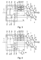
- FIG. 3 shows a circuit arrangement according to the invention for driving power semiconductor switches for a three-phase bridge circuit of the circuit breaker.
- FIG. 4 shows a circuit arrangement according to the invention for driving power semiconductor switches for a three-phase bridge circuit with a brake chopper.
- FIG. 1 shows a circuit arrangement for controlling power semiconductor switches according to the prior art. Shown is a half-bridge circuit consisting of a first power switch (40), the TOP switch and a second power switch (50), the BOT switch, arranged in series therewith.
- both switches each comprise a power transistor, for example an IGBT (insulated gate bipolar transistor) and an antiparallel-connected freewheeling diode or, alternatively, a MOSFET.
- the respective power switch can also consist of a plurality of parallel-connected IGBTs and a plurality of freewheeling diodes connected in antiparallel thereto or, analogously, a plurality of MOS-FETs.
- the control inputs, the gates of the respective transistors are connected to a driver circuit.
- the TOP switch (40) in this case the driver circuit (20) and the BOT switch (50) associated with the driver circuit (30).
- the two power switches are in operation at different potential, therefore, the two driver circuits (20, 30) must be arranged electrically isolated from each other.
- the control signals (5) of a higher-level controller are processed in the drive logic circuit (10) and transmitted galvanically separated to the driver circuits.
- the transformer (22, 32) connected.
- the transmitter (32) to the driver (30) of the BOT switch (50) is omitted according to the prior art. Then the drive logic (10) and the BOT driver (30) are at the same potential.
- FIG. 2 shows a circuit arrangement according to the invention for controlling power semiconductor switches for a half-bridge circuit of these power switches.
- the half-bridge circuit is identical to that in FIG. 1.
- IGBTs of the voltage class 1200V are provided here.
- the control signals (5) of the higher-level control are processed according to the invention by a single component and fed to the gates of the respective power switches (40, 50).
- the module in turn consists of two drive chips (72, 74), which are arranged isolated from each other in a common housing (70).
- the first drive chip (72) comprises a logic module (750), a driver (732) for the BOT switch (50) and a first level shifter (730) for a TOP switch.
- the output of this level shifter is connected to the input of the second drive chip (74).
- the signal between the logic module (750) and the driver (746) of the TOP switch (40) is thus by means of second level shifter (730, 740) on the necessary Potential raised. Since the first level shifter (730) is an integral part of the first drive chip (72) and the second level shifter (740) is an integral part of the second drive chip (74), each drive chip (72, 74) only has to overcome half the maximum voltage as a potential difference become. In this case, the ground potential of the first drive chip (72) can vary, for example, between 0V and 600V and that of the second drive chip (74) between 600V and 1200V. Thus, prior art 600V isolation techniques, such as SOI, can be used on the respective drive chip (72, 74).
- prior art 600V isolation techniques such as SOI
- both drive chips (72, 74) are arranged insulated from one another, the double potential difference is thus overcome compared to the potential difference of the respective drive chip (72, 74) in the entire integrated circuit arrangement.
- an integrated circuit arrangement (70) according to the invention for the voltage class of 1200V is realized.
- FIG. 3 shows a circuit arrangement according to the invention for driving power semiconductor switches for a three-phase bridge circuit of the circuit breaker.
- the three-phase bridge circuit is constructed of three half-bridge circuits identical to those in FIG.
- the three-phase bridge circuit has three TOP and three BOT switches, which are also designed as IGBTs of the 1200V voltage class.
- the load (60) can be configured, for example, as a three-phase electric motor.
- the control signals (5) of the higher-level control are processed according to the invention by a single component (70) and supplied to the gates of the respective power switches (40, 50) of the three-phase bridge circuit.
- the module (70) in turn consists of four drive chips (72, 74), which are arranged isolated from each other in a common housing (70).
- the first drive chip (72) is shown here in a higher complexity compared with FIG. 2 and comprises the functional groups voltage regulator (724) input interface (720), processing logic (722), fault management (726) and protection circuit (728) as well as three drivers (732 ) for the BOT switches (50) and three level shifters (730) for the TOP switches (40) of the three-phase bridge circuit.
- the outputs of the level shifters (730) are connected to the inputs of three second drive chips (74). These each comprise a level shifter (740), a signal reconstruction (742), a processing logic and a protection circuit (744) and the driver (746) of the respective TOP switch (40).
- the signal between the processing logic (722) and the driver (746) of the TOP switch (40) is in turn by means of second level shifter (730, 740) to the necessary Potential raised.
- the first level shifter (730) is an integral part of the first drive chip (72) and the second level shifter (740) an integral part of the respective second drive chip (74), wherein the output potential of the respective second drive chips (74) in operation at different potential between 600V and 1200V and this potential fluctuates during operation.
- FIG. 4 shows a circuit arrangement according to the invention for driving power semiconductor switches for a three-phase bridge circuit with a brake chopper.
- a seventh power switch (80) is arranged in addition to the three TOP and the three BOT switches (50).
- This seventh switch (80) is used in operation as a control for a so-called. Bremschopper, which serves the removal of excess electrical energy in a circuit example of the return of the electric motor (60).
- the first drive chip has an additional driver (734) compared to that shown in FIG. 3, which is at the same potential as the drivers (732) of the BOT switches (50).
Abstract
Description
Es wird eine integrierte Schaltungsanordnung vorgestellt zur Ansteuerung von Leistungshalbleiterschaltern angeordnet als Einzelschalter oder in einer Brückenschaltung. Derartige Brückenanordnungen von Leistungsschaltern sind als Ein-, Zwei-, oder Dreiphasen- Halbbrückenschaltungen bzw. als H- Brückenschaltungen bekannt, wobei die einphasige Halbbrücke einen Grundbaustein leistungselektronischer Schaltungen darstellt. In einer Halbbrückenschaltung sind zwei Leistungsschalter, ein erster, sog. TOP- Schalter und ein zweiter sog. BOT- Schalter in einer Reihenschaltung angeordnet. Eine derartige Halbbrücke weist in der Regel eine Verbindung zu einem Gleichstromzwischenkreis auf. Die Mittelanzapfung ist typischerweise mit einer Last verbunden.An integrated circuit arrangement is presented for controlling power semiconductor switches arranged as a single switch or in a bridge circuit. Such bridge arrangements of circuit breakers are known as one, two, or three-phase half-bridge circuits or as H-bridge circuits, wherein the single-phase half-bridge represents a basic building block of power electronic circuits. In a half-bridge circuit, two power switches, a first, so-called. TOP switch and a second so-called. BOT switch are arranged in a series circuit. Such a half-bridge usually has a connection to a DC intermediate circuit. The center tap is typically associated with a load.
Bei Ausgestaltung der Leistungsschalter mit einem Leistungshalbleiterbauelement oder mit einer Mehrzahl gleichartiger in Reihe geschalteter Leistungshalbleiterbauelemente ist zur Ansteuerung der Leistungsschalter eine Ansteuerschaltung notwendig. Diese Ansteuerschaltungen bestehen in der Regel nach dem Stand der Technik aus mehreren Teilschaltungen bzw. Funktionsblöcken. Das von einer übergeordneten Steuerung kommende Ansteuersignal wird in einer ersten Teilschaltung, der Ansteuerlogik, aufbereitet und über weitere Komponenten den Treiberschaltungen und schließlich dem Steuereingang des jeweiligen Leistungsschalters zugeführt. Bei Halbbrückenanordnungen mit höheren Zwischenkreisspannungen, beispielhaft größer 100V, wird die Ansteuerlogik zur Aufbereitung der Steuersignale potentialmäßig / galvanisch von den Treiberschaltungen getrennt, da sich die zugehörigen Leistungsschalter untereinander auf unterschiedlichem Potential befinden und somit eine spannungsmäßige Isolation unumgänglich wird. Diese Trennung erfolgt nach dem Stand der Technik beispielhaft mittels Übertragern, Optokopplern bzw. Lichtwellenleitern. Diese galvanische Trennung gilt zumindest für den TOP-Schalter, wird aber bei höheren Leistungen auch für den BOT- Schalter auf Grund eines möglichen Verrisses des Massepotentials beim Schalten ausgeführt.In the embodiment of the power switch with a power semiconductor component or with a plurality of similar series-connected power semiconductor components, a drive circuit is necessary for driving the power switch. As a rule, these drive circuits consist of a plurality of subcircuits or function blocks according to the prior art. The control signal coming from a higher-level control is processed in a first sub-circuit, the control logic, and supplied via further components to the driver circuits and finally to the control input of the respective circuit breaker. In half-bridge arrangements with higher DC link voltages, exemplarily greater than 100V, the control logic for the preparation of the control signals in terms of potential / galvanically separated from the driver circuits, since the associated circuit breakers are at different potential and thus a voltage isolation is inevitable. This separation takes place according to the prior art by way of example by means of transformers, Optocouplers or optical waveguides. This galvanic isolation applies at least to the TOP switch, but is also carried out at higher powers for the BOT switch due to a possible distortion of the ground potential during switching.
Bekannt sind auch integrierte Schaltungsanordnungen für Leistungsschalter der Spannungsklassen bis 600V, die auf eine externe galvanische Trennung verzichten. Dies sind monolithisch integrierte Schaltungen, wobei nach dem Stand der Technik Levelshifter beispielhaft in sog. SOI- (silicon on isolator) Technologie zur galvanischen Trennung der Ansteuerlogik von der eigentlichen Treiberschaltung eingesetzt werden. Für höhere Spannungsklassen steht diese Technologie technisch eingeschränkt und nur zu hohen Kosten zur Verfügung.Also known are integrated circuit arrangements for circuit breakers of the voltage classes up to 600V, which dispense with an external galvanic isolation. These are monolithically integrated circuits, wherein according to the prior art level shifters are used by way of example in so-called SOI (silicon on isolator) technology for galvanic isolation of the drive logic of the actual driver circuit. For higher voltage classes, this technology is technically limited and only available at high cost.
Weiterhin bekannt ist die monolithische Integration der Ansteuerlogik, sowie der Treiberschaltungen mittels "junction isolation". Diese Technik steht bis zur Spannungsklasse von 1200V zur Verfügung. Eine derartige Ausgestaltung der integrierten Schaltungsanordnung ist allerdings herstellungstechnisch sehr aufwändig und somit ebenso kostenintensiv. Weiterhin gibt es technische Probleme, beispielhaft mit Leckströmen und Latch-up Effekten u.a. bei höheren Temperaturen (>125°C Betriebstemperatur) sowie durch Verriß des Massepotentials bei schnellen dynamischen Vorgängen.Also known is the monolithic integration of the drive logic, as well as the driver circuits by means of "junction isolation". This technology is available up to the voltage class of 1200V. Such an embodiment of the integrated circuit arrangement, however, is very expensive in terms of production technology and thus also expensive. Furthermore, there are technical problems, for example with leakage currents and latch-up effects u.a. at higher temperatures (> 125 ° C operating temperature) as well as by a breakdown of the ground potential during fast dynamic processes.
Der Erfindung liegt die Aufgabe zugrunde eine integrierte Schaltungsanordnung vorzustellen, die bekannte Herstellungstechnologien verwendet und dabei für höhere Spannungsklassen einsetzbar ist als dies mit diesen Herstellungstechnologien üblich ist und gleichzeitig auch zum Einsatz bei höheren Betriebstemperaturen über 125°C geeignet ist.The invention has for its object to provide an integrated circuit arrangement that uses known manufacturing technologies and can be used for higher voltage classes than is usual with these manufacturing technologies and at the same time suitable for use at higher operating temperatures above 125 ° C.
Die Aufgabe wird erfindungsgemäß gelöst, durch die Maßnahmen der Merkmale der Ansprüche 1 oder 2. Bevorzugte Ausführungsformen sind in den Unteransprüchen beschrieben.The object is achieved by the measures of the features of claims 1 or 2. Preferred embodiments are described in the subclaims.
Die erfindungsgemäße integrierte Schaltungsanordnung dient der Ansteuerung von Leistungshalbleiterschaltern angeordnet als Einzelschalter oder in einer Brückenschaltung. Die Brückenschaltung ist hierbei die geläufigere Anwendung, daher wird im Folgenden hauptsächlich hierauf eingegangen. In Brückenschaltungen sind der TOP- und BOT- Schalter in Reihe geschaltet und mit einem Gleichstromzwischenkreis und einer Last verbunden. Die Brückenschaltung kann hierbei verschieden ausgestaltet sein, beispielsweise als ein-, zwei- oder dreiphasige Halbbrücke oder auch als Dreiphasenbrücke mit einem weiteren Leistungsschalter, dem sog. Bremschopper. Abhängig von der Ausgestaltung der Brückenschaltung weist die erfindungsgemäße integrierte Schaltungsanordnung einen ersten integrierten Ansteuerchip und mindestens einen zweiten integrierten Ansteuerchip auf. Der erste Ansteuerchip beinhaltet eine Mehrzahl von Funktionsgruppen, darunter die Ansteuerlogik und mindestens einen Treiber eines BOT-Schalters und mindestens einen ersten Levelshifter für einen TOP- Schalter. Der mindestens eine zweite integrierte Ansteuerchip enthält eine Mehrzahl von Funktionsgruppen darunter erfindungsgemäß mindestens einen zweiten Levelshifter und einen Treiber eines TOP- Schalters. Erfindungsgemäß ist der mindestens eine zweite Ansteuerchip dem ersten nachgeschaltet. Hierbei liegt das Grundpotential des jeweiligen zweiten Ansteuerchips auf dem Ausgangspotential des Levelshifters des ersten Ansteuerchips für den entsprechenden TOP- Schalter. Der erste und der mindestens eine zweite Ansteuerchip sind vorteilhafterweise in einem gemeinsamen Gehäuse mit geeigneter Isolierung aller Ansteuerchips gegeneinander angeordnet.The integrated circuit arrangement according to the invention serves to control power semiconductor switches arranged as individual switches or in a bridge circuit. The bridge circuit is here the more common application, therefore, mainly will be discussed in the following. In bridge circuits, the TOP and BOT switches are connected in series and connected to a DC link and a load. The bridge circuit can be designed differently, for example, as a one, two or three-phase half-bridge or as a three-phase bridge with another circuit breaker, the so-called brake chopper. Depending on the design of the bridge circuit, the integrated circuit arrangement according to the invention has a first integrated drive chip and at least one second integrated drive chip. The first drive chip includes a plurality of functional groups, including the drive logic and at least one driver of a BOT switch and at least a first level shifter for a TOP switch. The at least one second integrated drive chip contains a plurality of functional groups including, according to the invention, at least one second level shifter and a driver of a TOP switch. According to the invention, the at least one second drive chip is connected downstream of the first. In this case, the basic potential of the respective second drive chip lies at the output potential of the level shifter of the first drive chip for the corresponding TOP switch. The first and the at least one second drive chip are advantageously arranged in a common housing with suitable insulation of all drive chips against each other.
Im Falle der Ansteuerung eines Einzelschalters ist selbstverständliche kein Treiber für einen BOT- Schalter in der Schaltungsanordnung vorhanden sondern ausschließlich der oder die Levelshifter für den oder die auf anderem Potential liegenden Leistungsschalter.In the case of the control of a single switch is of course no driver for a BOT switch in the circuit arrangement available but only the or the level shifter for or the lying at another potential circuit breaker.
Der erfinderische Gedanke wird anhand der Ausführungsbeispiele in den Fig. 1 bis 4 näher erläutert.The inventive idea will be explained in more detail with reference to the embodiments in FIGS. 1 to 4.
Fig. 1 zeigt eine Schaltungsanordnung zur Ansteuerung von Leistungshalbleiterschaltern nach dem Stand der Technik.1 shows a circuit arrangement for controlling power semiconductor switches according to the prior art.
Fig. 2 zeigt eine erfindungsgemäße Schaltungsanordnung zur Ansteuerung von Leistungshalbleiterschaltern für eine Halbbrückenschaltung der Leistungsschalter.Fig. 2 shows a circuit arrangement according to the invention for driving power semiconductor switches for a half-bridge circuit of the circuit breaker.
Fig. 3 zeigt eine erfindungsgemäße Schaltungsanordnung zur Ansteuerung von Leistungshalbleiterschaltern für eine Dreiphasenbrückenschaltung der Leistungsschalter.FIG. 3 shows a circuit arrangement according to the invention for driving power semiconductor switches for a three-phase bridge circuit of the circuit breaker.
Fig. 4 zeigt eine erfindungsgemäße Schaltungsanordnung zur Ansteuerung von Leistungshalbleiterschaltern für eine Dreiphasenbrückenschaltung mit Bremschopper.4 shows a circuit arrangement according to the invention for driving power semiconductor switches for a three-phase bridge circuit with a brake chopper.
Fig. 1 zeigt eine Schaltungsanordnung zur Ansteuerung von Leistungshalbleiterschaltern nach dem Stand der Technik. Dargestellt ist eine Halbbrückenschaltung bestehend aus einem ersten Leistungsschalter (40), dem TOP-Schalter und einem in Reihe hierzu angeordneten zweiten Leistungsschalter (50), dem BOT- Schalter. Beide Schalter bestehen ihrerseits aus jeweils einem Leistungstransistor beispielhafte einem IGBT (insulated gate bipolar transistor) und einer antiparallel geschalteten Freilaufdiode oder alternativ hierzu einem MOS-FET. Dem Stand der Technik entsprechend kann der jeweilige Leistungsschalter auch aus einer Mehrzahl parallel geschalteter IGBTs und einer Mehrzahl antiparallel hierzu geschalteter Freilaufdioden bzw. analog eine Mehrzahl von MOS-FETs bestehen.1 shows a circuit arrangement for controlling power semiconductor switches according to the prior art. Shown is a half-bridge circuit consisting of a first power switch (40), the TOP switch and a second power switch (50), the BOT switch, arranged in series therewith. For their part, both switches each comprise a power transistor, for example an IGBT (insulated gate bipolar transistor) and an antiparallel-connected freewheeling diode or, alternatively, a MOSFET. According to the state of the art, the respective power switch can also consist of a plurality of parallel-connected IGBTs and a plurality of freewheeling diodes connected in antiparallel thereto or, analogously, a plurality of MOS-FETs.
Die Steuereingänge, die Gates der jeweiligen Transistoren sind mit einer Treiberschaltung verbunden. Dem TOP- Schalter (40) ist hierbei die Treiberschaltung (20) und dem BOT- Schalter (50) die Treiberschaltung (30) zugeordnet. Die beiden Leistungsschalter liegen im Betrieb auf unterschiedlichem Potential, daher müssen die beiden Treiberschaltungen (20, 30) elektrisch isoliert voneinander angeordnet sein.The control inputs, the gates of the respective transistors are connected to a driver circuit. The TOP switch (40) in this case the driver circuit (20) and the BOT switch (50) associated with the driver circuit (30). The two power switches are in operation at different potential, therefore, the two driver circuits (20, 30) must be arranged electrically isolated from each other.
Die Ansteuersignale (5) einer übergeordneten Steuerung werden in der Ansteuerlogikschaltung (10) aufbereitet und galvanisch getrennt zu den Treiberschaltungen übertragen. Zur galvanische Trennung sind hierbei zwischen der Ansteuerlogik (10) und den Treiberschaltungen (20, 30) die Übertrager (22, 32) geschaltet. In bestimmten Anwendungsfällen, beispielhaft bei kleinen Leistungen, wird nach dem Stand der Technik auf den Übertrager (32) zum Treiber (30) des BOT- Schalters (50) verzichtet. Dann befinden sich die Ansteuerlogik (10) und der BOT- Treiber (30) auf dem gleichen Potential.The control signals (5) of a higher-level controller are processed in the drive logic circuit (10) and transmitted galvanically separated to the driver circuits. For galvanic isolation in this case between the drive logic (10) and the driver circuits (20, 30), the transformer (22, 32) connected. In certain applications, for example, at low power, the transmitter (32) to the driver (30) of the BOT switch (50) is omitted according to the prior art. Then the drive logic (10) and the BOT driver (30) are at the same potential.
Fig. 2 zeigt eine erfindungsgemäße Schaltungsanordnung zur Ansteuerung von Leistungshalbleiterschaltern für eine Halbbrückenschaltung dieser Leistungsschalter. Die Halbbrückenschaltung ist identisch derjenigen in Fig. 1. Als Leistungsschalter (40, 50) sind hier IGBTs der Spannungsklasse 1200V vorgesehen.FIG. 2 shows a circuit arrangement according to the invention for controlling power semiconductor switches for a half-bridge circuit of these power switches. The half-bridge circuit is identical to that in FIG. 1. As power switches (40, 50), IGBTs of the voltage class 1200V are provided here.
Die Ansteuersignale (5)der übergeordneten Steuerung werden erfindungsgemäß von einem einzigen Baustein verarbeitet und den Gates der jeweiligen Leistungsschalter (40, 50) zugeführt. Der Baustein besteht seinerseits aus zwei Ansteuerchips (72, 74), die gegeneinander isoliert in einem gemeinsamen Gehäuse (70) angeordnet sind. Der erste Ansteuerchip (72) umfasst eine Logikbaugruppe (750), einen Treiber (732) für den BOT-Schalter (50) sowie einen ersten Levelshifter (730) für einen TOP- Schalter. Der Ausgang dieses Levelshifters ist mit dem Eingang des zweiten Ansteuerchips (74) verbunden. Dieser umfasst einen zweiten Levelshifter (740) sowie den Treiber (746) des TOP- Schalters (40).The control signals (5) of the higher-level control are processed according to the invention by a single component and fed to the gates of the respective power switches (40, 50). The module in turn consists of two drive chips (72, 74), which are arranged isolated from each other in a common housing (70). The first drive chip (72) comprises a logic module (750), a driver (732) for the BOT switch (50) and a first level shifter (730) for a TOP switch. The output of this level shifter is connected to the input of the second drive chip (74). This includes a second level shifter (740) and the driver (746) of the TOP switch (40).
Das Signal zwischen der Logikbaugruppe (750) und dem Treiber (746) des TOP-Schalters (40) wird somit mittels zweiter Levelshifter (730, 740) auf das notwendige Potential angehoben. Da der erste Levelshifter (730) integraler Bestandteil des ersten Ansteuerchips (72) ist und der zweite Levelshifter (740) integraler Bestandteil des zweiten Ansteuerchips (74) ist, muss auf jedem Ansteuerchip (72, 74) nur die halbe maximale Spannung als Potentialdifferenz überwunden werden. Hierbei kann das Grundpotential des ersten Ansteuerchips (72) beispielhaft zwischen 0V und 600V und das des zweiten Ansteuerchips (74) zwischen 600V und 1200V schwanken. Somit können 600V-Isolationsverfahren nach dem Stand der Technik, beispielhaft SOI, auf dem jeweiligen Ansteuerchip (72, 74) eingesetzt werden. Da beide Ansteuerchips (72, 74) gegeneinander isoliert angeordnet sind, wird somit die doppelte Potentialdifferenz verglichen mit der Potentialdifferenz des jeweiligen Ansteuerchips (72, 74) in der gesamten integrierten Schaltungsanordnung überwunden. Im Ausführungsbeispiel wird mit einer internen Isolierung innerhalb der Ansteuerchips (72, 74) von 600V, eine erfindungsgemäße integrierte Schaltungsanordnung (70) für die Spannungsklasse von 1200V realisiert.The signal between the logic module (750) and the driver (746) of the TOP switch (40) is thus by means of second level shifter (730, 740) on the necessary Potential raised. Since the first level shifter (730) is an integral part of the first drive chip (72) and the second level shifter (740) is an integral part of the second drive chip (74), each drive chip (72, 74) only has to overcome half the maximum voltage as a potential difference become. In this case, the ground potential of the first drive chip (72) can vary, for example, between 0V and 600V and that of the second drive chip (74) between 600V and 1200V. Thus, prior art 600V isolation techniques, such as SOI, can be used on the respective drive chip (72, 74). Since both drive chips (72, 74) are arranged insulated from one another, the double potential difference is thus overcome compared to the potential difference of the respective drive chip (72, 74) in the entire integrated circuit arrangement. In the exemplary embodiment, with an internal insulation within the drive chips (72, 74) of 600V, an integrated circuit arrangement (70) according to the invention for the voltage class of 1200V is realized.
Fig. 3 zeigt eine erfindungsgemäße Schaltungsanordnung zur Ansteuerung von Leistungshalbleiterschaltern für eine Dreiphasenbrückenschaltung der Leistungsschalter. Die Dreiphasenbrückenschaltung ist aus drei Halbbrückenschaltungen identisch derjenigen in Fig. 1 aufgebaut. Die Dreiphasenbrückenschaltung weist jeweils drei TOP- sowie drei BOT- Schalter auf, die ebenfalls als IGBTs der Spannungsklasse 1200V ausgebildet sind. Die Last (60) kann beispielhaft als Drehstrom- Elektromotor ausgebildet sein.FIG. 3 shows a circuit arrangement according to the invention for driving power semiconductor switches for a three-phase bridge circuit of the circuit breaker. The three-phase bridge circuit is constructed of three half-bridge circuits identical to those in FIG. The three-phase bridge circuit has three TOP and three BOT switches, which are also designed as IGBTs of the 1200V voltage class. The load (60) can be configured, for example, as a three-phase electric motor.
Die Ansteuersignale (5) der übergeordneten Steuerung werden erfindungsgemäß von einem einzigen Baustein (70) verarbeitet und den Gates der jeweiligen Leistungsschalter (40, 50) der Dreiphasenbrückenschaltung zugeführt. Der Baustein (70) besteht seinerseits aus vier Ansteuerchips (72, 74), die gegeneinander isoliert in einem gemeinsamen Gehäuse (70) angeordnet sind. Der erste Ansteuerchip (72) ist hier in einer höheren Komplexität verglichen mit Fig. 2 dargestellt und umfasst die Funktionsgruppen Spannungsregler (724) Eingangsinterface (720), Verarbeitungslogik (722), Fehlermanagement (726) und Schutzschaltung (728) sowie drei Treiber (732) für die BOT-Schalter (50) und drei Levelshifter (730) für die TOP- Schalter (40) der Dreiphasenbrückenschaltung. Die Ausgänge der Levelshifter (730) sind mit den Eingängen von drei zweiten Ansteuerchips (74) verbunden. Diese umfassen jeweils einen Levelshifter (740), eine Signalrekonstruktion (742), eine Verarbeitungslogik und eine Schutzschaltung (744) sowie den Treiber (746) des jeweiligen TOP- Schalters (40).The control signals (5) of the higher-level control are processed according to the invention by a single component (70) and supplied to the gates of the respective power switches (40, 50) of the three-phase bridge circuit. The module (70) in turn consists of four drive chips (72, 74), which are arranged isolated from each other in a common housing (70). The first drive chip (72) is shown here in a higher complexity compared with FIG. 2 and comprises the functional groups voltage regulator (724) input interface (720), processing logic (722), fault management (726) and protection circuit (728) as well as three drivers (732 ) for the BOT switches (50) and three level shifters (730) for the TOP switches (40) of the three-phase bridge circuit. The outputs of the level shifters (730) are connected to the inputs of three second drive chips (74). These each comprise a level shifter (740), a signal reconstruction (742), a processing logic and a protection circuit (744) and the driver (746) of the respective TOP switch (40).
Das Signal zwischen der Verarbeitungslogik (722) und dem Treiber (746) des TOP-Schalters (40) wird wiederum mittels zweiter Levelshifter (730, 740) auf das notwendige Potential angehoben. Der erste Levelshifter (730) ist integraler Bestandteil des ersten Ansteuerchips (72) und der zweite Levelshifter (740) integraler Bestandteil des jeweiligen zweiten Ansteuerchips (74), wobei das Ausgangspotential der jeweiligen zweiten Ansteuerchips (74) im Betrieb auf unterschiedlichem Potential zwischen 600V und 1200V liegen und dieses Potential während der Betriebszeit schwankend ist. Auch im Fall der Ansteuerung einer Dreiphasenbrückenschaltung können Isolationsverfahren nach dem Stand der Technik auf dem jeweiligen Ansteuerchip (72, 74) eingesetzt werden. Da alle Ansteuerchips (72, 74) gegeneinander isoliert angeordnet sind kann somit ebenfalls wie im Ausführungsbeispiel gemäß Fig. 2 die doppelte Potentialdifferenz, verglichen mit der Potentialdifferenz innerhalb eines Ansteuerchips (72, 74) in der gesamten integrierten Schaltungsanordnung (70) überwunden werden.The signal between the processing logic (722) and the driver (746) of the TOP switch (40) is in turn by means of second level shifter (730, 740) to the necessary Potential raised. The first level shifter (730) is an integral part of the first drive chip (72) and the second level shifter (740) an integral part of the respective second drive chip (74), wherein the output potential of the respective second drive chips (74) in operation at different potential between 600V and 1200V and this potential fluctuates during operation. Even in the case of driving a three-phase bridge circuit isolation methods according to the prior art on the respective drive chip (72, 74) can be used. Since all the drive chips (72, 74) are arranged isolated from each other can thus also as in the embodiment of FIG. 2, the double potential difference, compared with the potential difference within a Ansteuerchips (72, 74) in the entire integrated circuit (70) are overcome.
Fig. 4 zeigt eine erfindungsgemäße Schaltungsanordnung zur Ansteuerung von Leistungshalbleiterschaltern für eine Dreiphasenbrückenschaltung mit Bremschopper. Hierbei ist ein siebter Leistungsschalter (80) zusätzliche zu den drei TOP-, und den drei BOT- Schaltern (50) angeordnet. Dieser siebte Schalter (80) dient im Betrieb als Steuerung für einen sog. Bremschopper, welcher der Abführung überschüssiger elektrischer Energie in einer Schaltung beispielhaft aus der Rückspeisung des Elektromotors (60) dient. Zur Ansteuerung des Leistungsschalters (80) für den Bremschopper weist der erste Ansteuerchip gegenüber demjenigen gemäß Fig. 3 einen weiteren Treiber (734) auf, der auf dem gleichen Potential wie die Treiber (732) der BOT- Schalter (50) liegt.4 shows a circuit arrangement according to the invention for driving power semiconductor switches for a three-phase bridge circuit with a brake chopper. Here, a seventh power switch (80) is arranged in addition to the three TOP and the three BOT switches (50). This seventh switch (80) is used in operation as a control for a so-called. Bremschopper, which serves the removal of excess electrical energy in a circuit example of the return of the electric motor (60). In order to control the circuit breaker (80) for the brake chopper, the first drive chip has an additional driver (734) compared to that shown in FIG. 3, which is at the same potential as the drivers (732) of the BOT switches (50).
Claims (9)
wobei die Schaltungsanordnung aus einem ersten integrierten Ansteuerchip (72) mit einer Mehrzahl von Funktionsgruppen besteht mindestens umfassend mindestens einen ersten Levelshifter (730) für einen Schalter (40),
und mindestens einem zweiten integrierten Ansteuerchip (74) mit einer Mehrzahl von Funktionsgruppen mindestens umfassend einen zweiten Levelshifter (740) und einen Treiber (746) eines Schalters (40),
wobei der mindestens eine zweite Ansteuerchip (74) dem ersten (72) nachgeschaltet ist, sich das Grundpotential des zweiten Ansteuerchips (74) auf dem Ausgangspotential des Levelshifters (730) des ersten Ansteuerchips (72) befindet und die Ansteuerchips (72, 74) in einem gemeinsamen Gehäuse (70) mit geeigneter Isolierung der Ansteuerchips (72, 74) gegeneinander angeordnet sind.Integrated circuit arrangement for controlling power semiconductor switches (40),
wherein the circuit arrangement comprises a first integrated drive chip (72) having a plurality of functional groups, at least comprising at least one first level shifter (730) for a switch (40),
and at least one second integrated drive chip (74) having a plurality of functional groups, at least comprising a second level shifter (740) and a driver (746) of a switch (40),
wherein the at least one second drive chip (74) is connected downstream of the first (72), the ground potential of the second drive chip (74) is at the output potential of the level shifter (730) of the first drive chip (72) and the drive chips (72, 74) in a common housing (70) with suitable insulation of the drive chips (72, 74) are arranged against each other.
wobei die Schaltungsanordnung aus einem ersten integrierten Ansteuerchip (72) mit einer Mehrzahl von Funktionsgruppen besteht mindestens umfassend einen Treiber (732) eines BOT- Schalters (50) und mindestens einen ersten Levelshifter (730) für einen TOP- Schalter (40),
und mindestens einem zweiten integrierten Ansteuerchip (74) mit einer Mehrzahl von Funktionsgruppen mindestens umfassend einen zweiten Levelshifter (740) und einen Treiber (746) eines TOP- Schalters (40),
wobei der mindestens eine zweite Ansteuerchip (74) dem ersten (72) nachgeschaltet ist, sich das Grundpotential des zweiten Ansteuerchips (74) auf dem Ausgangspotential des Levelshifters (730) des ersten Ansteuerchips (72) befindet und die Ansteuerchips (72, 74) in einem gemeinsamen Gehäuse (70) mit geeigneter Isolierung der Ansteuerchips (72, 74) gegeneinander angeordnet sind.Integrated circuit arrangement for controlling power semiconductor switches (40, 50) arranged in a bridge circuit as a TOP (40) and BOT (50) switch connected to a DC intermediate circuit and a load (60),
wherein the circuit arrangement comprises a first integrated drive chip (72) having a plurality of functional groups, at least comprising a driver (732) of a BOT switch (50) and at least one first level shifter (730) for a TOP switch (40),
and at least one second integrated drive chip (74) having a plurality of functional groups, at least comprising a second level shifter (740) and a driver (746) of a TOP switch (40),
wherein the at least one second drive chip (74) is connected downstream of the first (72), the ground potential of the second drive chip (74) is at the output potential of the level shifter (730) of the first drive chip (72) and the drive chips (72, 74) in a common housing (70) with suitable insulation of the drive chips (72, 74) are arranged against each other.
wobei ein Leistungshalbleiterschalter (40, 50) ein oder eine Mehrzahl gleichartiger Leistungshalbleiterbauelemente wie IGBTs mit antiparallel dazu angeordneter Freilaufdiode oder MOSFETs aufweist.Circuit arrangement according to Claim 1 or 2,
wherein a power semiconductor switch (40, 50) has one or a plurality of similar power semiconductor components such as IGBTs with antiparallel arranged freewheeling diode or MOSFETs.
wobei der erste integrierte Ansteuerchip (72) die weiteren Funktionsgruppen Spannungsregler (724), Eingangsinterface (720), Verarbeitungslogik (722), Fehlermanagement (726)und Schutzschaltung (728) aufweist.Circuit arrangement according to Claim 1 or 2,
wherein the first integrated drive chip (72) has the further functional groups voltage regulator (724), input interface (720), processing logic (722), error management (726) and protection circuit (728).
wobei ein zweiter integrierter Ansteuerchip (74) die weiteren Funktionsgruppen Signalrekonstruktion (742), Verarbeitungslogik und Schutzschaltung (744) aufweist.Circuit arrangement according to Claim 1 or 2,
wherein a second integrated drive chip (74) has the further function groups signal reconstruction (742), processing logic and protection circuit (744).
wobei das Ausgangspotential des ersten Levelshifters (730) zwischen 0 und 600V oberhalb des Grundpotential des ersten integrierten Ansteuerchips (72) variiert.Circuit arrangement according to Claim 1 or 2,
wherein the output potential of the first level shifter (730) varies between 0 and 600V above the ground potential of the first integrated drive chip (72).
wobei die Schaltungsanordnung zur Ansteuerung der Leistungshalbleiterschalter (40, 50) einer Halbbrückenschaltungsanordnung bestehend aus je einem TOP- und einem BOT- Schalter einen ersten (72) und einen zweiten (74) Ansteuerchip aufweist.Circuit arrangement according to Claim 2,
wherein the circuit arrangement for controlling the power semiconductor switches (40, 50) of a half-bridge circuit arrangement each comprising a TOP and a BOT switch has a first (72) and a second (74) drive chip.
wobei die Schaltungsanordnung zur Ansteuerung der Leistungshalbleiterschalter (40, 50) einer 3-Phasen Brückenschaltungsanordnung einen ersten Ansteuerchip (72) mit drei BOT- Treibern (732) und drei Levelshiftern (730) sowie drei zweite Ansteuerchips (74) mit jeweils einem Levelshifter (740) und einem TOP-Treiber (746) aufweist.Circuit arrangement according to Claim 2,
wherein the circuit arrangement for controlling the power semiconductor switches (40, 50) of a 3-phase bridge circuit arrangement comprises a first drive chip (72) with three BOT drivers (732) and three level shifters (730) and three second drive chips (74) each with a level shifter (740 ) and a TOP driver (746).
wobei die Schaltungsanordnung zur Ansteuerung der Leistungshalbleiterschalter (40, 50) einer 3-Phasen Brückenschaltungsanordnung mit Bremschopper einen ersten Ansteuerchip (72) mit drei BOT- Treibern (732), einem Treiber (734) eines weiteren Schalters (80) für einen Bremschopper und drei Levelshiftern (730) sowie drei zweite Ansteuerchips (74) mit jeweils einem Levelshifter (740) und einem TOP-Treiber (746) aufweist.Circuit arrangement according to Claim 2,
wherein the circuit arrangement for controlling the power semiconductor switches (40, 50) of a 3-phase bridge circuit arrangement with a brake chopper has a first drive chip (72) with three BOT drivers (732), a driver (734) of a further switch (80) for a brake chopper and three Levelshiftern (730) and three second drive chips (74) each having a level shifter (740) and a TOP driver (746).
Applications Claiming Priority (1)
| Application Number | Priority Date | Filing Date | Title |
|---|---|---|---|
| DE102004049817A DE102004049817A1 (en) | 2004-10-13 | 2004-10-13 | Integrated circuit arrangement for controlling power semiconductor switches |
Publications (1)
| Publication Number | Publication Date |
|---|---|
| EP1648086A1 true EP1648086A1 (en) | 2006-04-19 |
Family
ID=35539339
Family Applications (1)
| Application Number | Title | Priority Date | Filing Date |
|---|---|---|---|
| EP05017562A Withdrawn EP1648086A1 (en) | 2004-10-13 | 2005-08-12 | Integrated circuit for controlling semiconductor power switches |
Country Status (6)
| Country | Link |
|---|---|
| US (1) | US20060087260A1 (en) |
| EP (1) | EP1648086A1 (en) |
| JP (1) | JP2006115472A (en) |
| KR (1) | KR100723373B1 (en) |
| CN (1) | CN1855679A (en) |
| DE (1) | DE102004049817A1 (en) |
Families Citing this family (5)
| Publication number | Priority date | Publication date | Assignee | Title |
|---|---|---|---|---|
| DE102005023652B3 (en) * | 2005-05-23 | 2006-08-03 | Semikron Elektronik Gmbh & Co. Kg | Circuit arrangement for controlling e.g. insulated gate bipolar transistor, has circuit part for detecting switching condition of TOP switch and for detecting and evaluating current flow through level shifter for controlling secondary side |
| DE102006050913B4 (en) * | 2006-10-28 | 2012-08-23 | Semikron Elektronik Gmbh & Co. Kg | Control circuit with BOT level shifter for transmitting an input signal and associated method |
| DE102007006319B4 (en) * | 2007-02-08 | 2012-12-13 | Semikron Elektronik Gmbh & Co. Kg | Control circuit with TOP level shifter for transmitting an input signal and associated method |
| US7977887B2 (en) * | 2008-09-09 | 2011-07-12 | Delphi Technologies, Inc. | Low leakage current LED drive apparatus with fault protection and diagnostics |
| US9678524B2 (en) * | 2015-09-25 | 2017-06-13 | Micron Technology, Inc. | Apparatuses and methods for power regulation based on input power |
Citations (4)
| Publication number | Priority date | Publication date | Assignee | Title |
|---|---|---|---|---|
| DE19611401A1 (en) * | 1996-03-22 | 1997-09-25 | Danfoss As | Frequency converter for an electric motor |
| US6114883A (en) * | 1997-07-15 | 2000-09-05 | Dialog Semiconductor Gmbh | Circuit for driving semiconductor switches |
| US6680630B1 (en) * | 2002-08-08 | 2004-01-20 | Mitsubishi Denki Kabushiki Kaisha | Driver circuit for power device |
| US6781423B1 (en) * | 2003-07-04 | 2004-08-24 | Dialog Semiconductor Gmbh | High-voltage interface and driver control circuit |
Family Cites Families (6)
| Publication number | Priority date | Publication date | Assignee | Title |
|---|---|---|---|---|
| JP2763237B2 (en) * | 1992-11-02 | 1998-06-11 | 株式会社日立製作所 | Level shift circuit and inverter device using the same |
| JP3493313B2 (en) * | 1998-12-07 | 2004-02-03 | シャープ株式会社 | Negative voltage level shifter circuit and nonvolatile semiconductor memory device |
| US6507226B2 (en) * | 2000-07-31 | 2003-01-14 | Intersil Americas Inc. | Power device driving circuit and associated methods |
| JP4462776B2 (en) * | 2001-03-13 | 2010-05-12 | 三菱電機株式会社 | Power converter and signal level converter |
| JP3806644B2 (en) * | 2001-12-13 | 2006-08-09 | 三菱電機株式会社 | Power semiconductor device |
| US6531895B1 (en) * | 2002-02-08 | 2003-03-11 | Delphi Technologies, Inc. | Isolated gate drive circuit having a switched input capacitor |
-
2004
- 2004-10-13 DE DE102004049817A patent/DE102004049817A1/en not_active Ceased
-
2005
- 2005-08-12 EP EP05017562A patent/EP1648086A1/en not_active Withdrawn
- 2005-08-15 JP JP2005235322A patent/JP2006115472A/en active Pending
- 2005-10-05 KR KR1020050093532A patent/KR100723373B1/en not_active IP Right Cessation
- 2005-10-11 US US11/247,319 patent/US20060087260A1/en not_active Abandoned
- 2005-10-12 CN CNA2005101067739A patent/CN1855679A/en active Pending
Patent Citations (4)
| Publication number | Priority date | Publication date | Assignee | Title |
|---|---|---|---|---|
| DE19611401A1 (en) * | 1996-03-22 | 1997-09-25 | Danfoss As | Frequency converter for an electric motor |
| US6114883A (en) * | 1997-07-15 | 2000-09-05 | Dialog Semiconductor Gmbh | Circuit for driving semiconductor switches |
| US6680630B1 (en) * | 2002-08-08 | 2004-01-20 | Mitsubishi Denki Kabushiki Kaisha | Driver circuit for power device |
| US6781423B1 (en) * | 2003-07-04 | 2004-08-24 | Dialog Semiconductor Gmbh | High-voltage interface and driver control circuit |
Non-Patent Citations (1)
| Title |
|---|
| LIN R L ET AL: "Single-power-supply-based transformerless IGBT/MOSFET gate driver with 100% high-side turn-on duty cycle operation performance using auxiliary bootstrapped charge pumper", POWER ELECTRONICS SPECIALISTS CONFERENCE, 1997. PESC '97 RECORD., 28TH ANNUAL IEEE ST. LOUIS, MO, USA 22-27 JUNE 1997, NEW YORK, NY, USA,IEEE, US, vol. 2, 22 June 1997 (1997-06-22), pages 1205 - 1209, XP010241701, ISBN: 0-7803-3840-5 * |
Also Published As
| Publication number | Publication date |
|---|---|
| DE102004049817A1 (en) | 2006-04-27 |
| KR100723373B1 (en) | 2007-05-30 |
| JP2006115472A (en) | 2006-04-27 |
| KR20060052050A (en) | 2006-05-19 |
| US20060087260A1 (en) | 2006-04-27 |
| CN1855679A (en) | 2006-11-01 |
Similar Documents
| Publication | Publication Date | Title |
|---|---|---|
| EP1920526B1 (en) | Converter circuit comprising distributed energy stores | |
| EP1887698B1 (en) | Level shifter for an actuator switch for power semiconductor components | |
| DE102007006319B4 (en) | Control circuit with TOP level shifter for transmitting an input signal and associated method | |
| DE112014003605B4 (en) | Drive control device for an electric motor | |
| EP1739835B1 (en) | Circuit for controlling semiconductor power switches with error detection | |
| DE102010018997B4 (en) | Drive circuit with transmission circuit for the capacitive transmission of a signal and associated method | |
| EP1670131A2 (en) | Power semiconductor module with reduced parasitic inductances | |
| EP2871766B1 (en) | Control circuit for three level inverter | |
| DE102013224022A1 (en) | Inverters with SiC JFETs | |
| EP1648086A1 (en) | Integrated circuit for controlling semiconductor power switches | |
| WO2015117691A1 (en) | Rectifier circuit with self-clamping transistor | |
| EP2871763B1 (en) | Control system for driving bridge circuits with a symmetrically grounded intermediate circuit | |
| DE102011055626A1 (en) | Device for controlling electric drive motor of steering system, has determination element that determines phase of current line of electric drive motor so as to activate drive element for controlling electric drive motor | |
| EP2705598A2 (en) | Drive unit for an electric motor | |
| EP2824837B1 (en) | Power semiconductor switch circuit | |
| DE102006038541B4 (en) | Semiconductor device arrangement with complementary power devices | |
| DE102016207254A1 (en) | Inverter, electric drive arrangement with an inverter | |
| DE102012206326A1 (en) | Power switch arrangement for e.g. permanent excited synchronous motor of motor car, has control unit that adjusts duration of dead-time phases lying between switch-on phases such that switching elements are switched-off in duration | |
| DE112018006066T5 (en) | Control circuit for a polyphase motor | |
| EP3462615A1 (en) | Optimized cascode structures | |
| DE102020007476A1 (en) | Inverter for controlling an electric motor of an electrically drivable vehicle | |
| DE102017203233A1 (en) | Modular inverter | |
| WO2022263233A1 (en) | Low-inductance busbar between half-bridge module and intermediate circuit | |
| EP1081765B1 (en) | Integrated circuit built in a substrate protected against a voltage reversal | |
| DE102011080270A1 (en) | Circuit breaker arrangement e.g. system-in-package has power switches, control logic for controlling activation of switches and insulating elements for control of switches and for isolation between control logic and switches |
Legal Events
| Date | Code | Title | Description |
|---|---|---|---|
| PUAI | Public reference made under article 153(3) epc to a published international application that has entered the european phase |
Free format text: ORIGINAL CODE: 0009012 |
|
| AK | Designated contracting states |
Kind code of ref document: A1 Designated state(s): AT BE BG CH CY CZ DE DK EE ES FI FR GB GR HU IE IS IT LI LT LU LV MC NL PL PT RO SE SI SK TR |
|
| AX | Request for extension of the european patent |
Extension state: AL BA HR MK YU |
|
| AKX | Designation fees paid |
Designated state(s): AT BE BG CH CY CZ DE DK EE ES FI FR GB GR HU IE IS IT LI LT LU LV MC NL PL PT RO SE SI SK TR |
|
| STAA | Information on the status of an ep patent application or granted ep patent |
Free format text: STATUS: THE APPLICATION IS DEEMED TO BE WITHDRAWN |
|
| 18D | Application deemed to be withdrawn |
Effective date: 20061020 |