EP1639452B1 - Method and apparatus for shuffling data - Google Patents
Method and apparatus for shuffling data Download PDFInfo
- Publication number
- EP1639452B1 EP1639452B1 EP04756204A EP04756204A EP1639452B1 EP 1639452 B1 EP1639452 B1 EP 1639452B1 EP 04756204 A EP04756204 A EP 04756204A EP 04756204 A EP04756204 A EP 04756204A EP 1639452 B1 EP1639452 B1 EP 1639452B1
- Authority
- EP
- European Patent Office
- Prior art keywords
- data
- operand
- shuffle
- resultant
- data element
- Prior art date
- Legal status (The legal status is an assumption and is not a legal conclusion. Google has not performed a legal analysis and makes no representation as to the accuracy of the status listed.)
- Active
Links
- 238000000034 method Methods 0.000 title claims abstract description 58
- 230000004044 response Effects 0.000 claims description 10
- 230000006870 function Effects 0.000 claims description 9
- 238000013461 design Methods 0.000 claims description 6
- 238000012545 processing Methods 0.000 description 44
- 238000007667 floating Methods 0.000 description 29
- 238000013500 data storage Methods 0.000 description 13
- 238000005516 engineering process Methods 0.000 description 12
- 238000010586 diagram Methods 0.000 description 11
- 230000008569 process Effects 0.000 description 9
- 238000003860 storage Methods 0.000 description 8
- 238000004891 communication Methods 0.000 description 7
- 101000912503 Homo sapiens Tyrosine-protein kinase Fgr Proteins 0.000 description 6
- 102100026150 Tyrosine-protein kinase Fgr Human genes 0.000 description 6
- 238000001914 filtration Methods 0.000 description 6
- 230000001419 dependent effect Effects 0.000 description 5
- 235000019580 granularity Nutrition 0.000 description 5
- 238000004519 manufacturing process Methods 0.000 description 5
- 101100285899 Saccharomyces cerevisiae (strain ATCC 204508 / S288c) SSE2 gene Proteins 0.000 description 4
- 239000003086 colorant Substances 0.000 description 4
- 230000003287 optical effect Effects 0.000 description 4
- 229910052760 oxygen Inorganic materials 0.000 description 4
- 239000000872 buffer Substances 0.000 description 3
- 230000007246 mechanism Effects 0.000 description 3
- 238000012546 transfer Methods 0.000 description 3
- 238000013459 approach Methods 0.000 description 2
- 230000008901 benefit Effects 0.000 description 2
- 230000006835 compression Effects 0.000 description 2
- 238000007906 compression Methods 0.000 description 2
- 238000004590 computer program Methods 0.000 description 2
- 230000006872 improvement Effects 0.000 description 2
- 230000000644 propagated effect Effects 0.000 description 2
- 230000008707 rearrangement Effects 0.000 description 2
- 230000003068 static effect Effects 0.000 description 2
- 230000009466 transformation Effects 0.000 description 2
- 102000001332 SRC Human genes 0.000 description 1
- 108060006706 SRC Proteins 0.000 description 1
- 230000005540 biological transmission Effects 0.000 description 1
- 229910052799 carbon Inorganic materials 0.000 description 1
- 230000001413 cellular effect Effects 0.000 description 1
- 230000008859 change Effects 0.000 description 1
- 238000006243 chemical reaction Methods 0.000 description 1
- 230000008878 coupling Effects 0.000 description 1
- 238000010168 coupling process Methods 0.000 description 1
- 238000005859 coupling reaction Methods 0.000 description 1
- 238000013479 data entry Methods 0.000 description 1
- 230000006837 decompression Effects 0.000 description 1
- 230000003247 decreasing effect Effects 0.000 description 1
- 238000001514 detection method Methods 0.000 description 1
- 238000011161 development Methods 0.000 description 1
- 235000019800 disodium phosphate Nutrition 0.000 description 1
- 238000006073 displacement reaction Methods 0.000 description 1
- 238000009826 distribution Methods 0.000 description 1
- 230000000694 effects Effects 0.000 description 1
- 229910052739 hydrogen Inorganic materials 0.000 description 1
- 238000003384 imaging method Methods 0.000 description 1
- 238000002513 implantation Methods 0.000 description 1
- 230000003993 interaction Effects 0.000 description 1
- 239000004973 liquid crystal related substance Substances 0.000 description 1
- 230000001343 mnemonic effect Effects 0.000 description 1
- 238000012986 modification Methods 0.000 description 1
- 230000004048 modification Effects 0.000 description 1
- 229910052757 nitrogen Inorganic materials 0.000 description 1
- 230000002093 peripheral effect Effects 0.000 description 1
- 229910052698 phosphorus Inorganic materials 0.000 description 1
- 238000013139 quantization Methods 0.000 description 1
- 239000004065 semiconductor Substances 0.000 description 1
- 238000012163 sequencing technique Methods 0.000 description 1
- 238000004088 simulation Methods 0.000 description 1
- 238000001228 spectrum Methods 0.000 description 1
- 230000001360 synchronised effect Effects 0.000 description 1
- 235000019587 texture Nutrition 0.000 description 1
- 238000000844 transformation Methods 0.000 description 1
Images


Classifications
-
- G—PHYSICS
- G06—COMPUTING; CALCULATING OR COUNTING
- G06F—ELECTRIC DIGITAL DATA PROCESSING
- G06F9/00—Arrangements for program control, e.g. control units
- G06F9/06—Arrangements for program control, e.g. control units using stored programs, i.e. using an internal store of processing equipment to receive or retain programs
- G06F9/30—Arrangements for executing machine instructions, e.g. instruction decode
- G06F9/30003—Arrangements for executing specific machine instructions
- G06F9/30007—Arrangements for executing specific machine instructions to perform operations on data operands
- G06F9/30032—Movement instructions, e.g. MOVE, SHIFT, ROTATE, SHUFFLE
-
- G—PHYSICS
- G06—COMPUTING; CALCULATING OR COUNTING
- G06F—ELECTRIC DIGITAL DATA PROCESSING
- G06F7/00—Methods or arrangements for processing data by operating upon the order or content of the data handled
- G06F7/76—Arrangements for rearranging, permuting or selecting data according to predetermined rules, independently of the content of the data
-
- G—PHYSICS
- G06—COMPUTING; CALCULATING OR COUNTING
- G06F—ELECTRIC DIGITAL DATA PROCESSING
- G06F9/00—Arrangements for program control, e.g. control units
- G06F9/06—Arrangements for program control, e.g. control units using stored programs, i.e. using an internal store of processing equipment to receive or retain programs
- G06F9/30—Arrangements for executing machine instructions, e.g. instruction decode
- G06F9/30003—Arrangements for executing specific machine instructions
- G06F9/30007—Arrangements for executing specific machine instructions to perform operations on data operands
- G06F9/3001—Arithmetic instructions
- G06F9/30014—Arithmetic instructions with variable precision
-
- G—PHYSICS
- G06—COMPUTING; CALCULATING OR COUNTING
- G06F—ELECTRIC DIGITAL DATA PROCESSING
- G06F9/00—Arrangements for program control, e.g. control units
- G06F9/06—Arrangements for program control, e.g. control units using stored programs, i.e. using an internal store of processing equipment to receive or retain programs
- G06F9/30—Arrangements for executing machine instructions, e.g. instruction decode
- G06F9/30003—Arrangements for executing specific machine instructions
- G06F9/30007—Arrangements for executing specific machine instructions to perform operations on data operands
- G06F9/30018—Bit or string instructions
-
- G—PHYSICS
- G06—COMPUTING; CALCULATING OR COUNTING
- G06F—ELECTRIC DIGITAL DATA PROCESSING
- G06F9/00—Arrangements for program control, e.g. control units
- G06F9/06—Arrangements for program control, e.g. control units using stored programs, i.e. using an internal store of processing equipment to receive or retain programs
- G06F9/30—Arrangements for executing machine instructions, e.g. instruction decode
- G06F9/30003—Arrangements for executing specific machine instructions
- G06F9/30007—Arrangements for executing specific machine instructions to perform operations on data operands
- G06F9/30036—Instructions to perform operations on packed data, e.g. vector, tile or matrix operations
-
- G—PHYSICS
- G06—COMPUTING; CALCULATING OR COUNTING
- G06F—ELECTRIC DIGITAL DATA PROCESSING
- G06F9/00—Arrangements for program control, e.g. control units
- G06F9/06—Arrangements for program control, e.g. control units using stored programs, i.e. using an internal store of processing equipment to receive or retain programs
- G06F9/30—Arrangements for executing machine instructions, e.g. instruction decode
- G06F9/30098—Register arrangements
- G06F9/30105—Register structure
- G06F9/30109—Register structure having multiple operands in a single register
-
- G—PHYSICS
- G06—COMPUTING; CALCULATING OR COUNTING
- G06F—ELECTRIC DIGITAL DATA PROCESSING
- G06F9/00—Arrangements for program control, e.g. control units
- G06F9/06—Arrangements for program control, e.g. control units using stored programs, i.e. using an internal store of processing equipment to receive or retain programs
- G06F9/30—Arrangements for executing machine instructions, e.g. instruction decode
- G06F9/30098—Register arrangements
- G06F9/3012—Organisation of register space, e.g. banked or distributed register file
- G06F9/3013—Organisation of register space, e.g. banked or distributed register file according to data content, e.g. floating-point registers, address registers
-
- G—PHYSICS
- G06—COMPUTING; CALCULATING OR COUNTING
- G06F—ELECTRIC DIGITAL DATA PROCESSING
- G06F9/00—Arrangements for program control, e.g. control units
- G06F9/06—Arrangements for program control, e.g. control units using stored programs, i.e. using an internal store of processing equipment to receive or retain programs
- G06F9/30—Arrangements for executing machine instructions, e.g. instruction decode
- G06F9/30145—Instruction analysis, e.g. decoding, instruction word fields
-
- G—PHYSICS
- G06—COMPUTING; CALCULATING OR COUNTING
- G06F—ELECTRIC DIGITAL DATA PROCESSING
- G06F9/00—Arrangements for program control, e.g. control units
- G06F9/06—Arrangements for program control, e.g. control units using stored programs, i.e. using an internal store of processing equipment to receive or retain programs
- G06F9/30—Arrangements for executing machine instructions, e.g. instruction decode
- G06F9/38—Concurrent instruction execution, e.g. pipeline, look ahead
- G06F9/3802—Instruction prefetching
-
- G—PHYSICS
- G06—COMPUTING; CALCULATING OR COUNTING
- G06F—ELECTRIC DIGITAL DATA PROCESSING
- G06F9/00—Arrangements for program control, e.g. control units
- G06F9/06—Arrangements for program control, e.g. control units using stored programs, i.e. using an internal store of processing equipment to receive or retain programs
- G06F9/30—Arrangements for executing machine instructions, e.g. instruction decode
- G06F9/38—Concurrent instruction execution, e.g. pipeline, look ahead
- G06F9/3885—Concurrent instruction execution, e.g. pipeline, look ahead using a plurality of independent parallel functional units
- G06F9/3887—Concurrent instruction execution, e.g. pipeline, look ahead using a plurality of independent parallel functional units controlled by a single instruction for multiple data lanes [SIMD]
-
- G—PHYSICS
- G06—COMPUTING; CALCULATING OR COUNTING
- G06F—ELECTRIC DIGITAL DATA PROCESSING
- G06F9/00—Arrangements for program control, e.g. control units
- G06F9/06—Arrangements for program control, e.g. control units using stored programs, i.e. using an internal store of processing equipment to receive or retain programs
- G06F9/30—Arrangements for executing machine instructions, e.g. instruction decode
- G06F9/30003—Arrangements for executing specific machine instructions
- G06F9/30007—Arrangements for executing specific machine instructions to perform operations on data operands
- G06F9/30025—Format conversion instructions, e.g. Floating-Point to Integer, decimal conversion
Abstract
Description
- This patent application is a Continuation In Part of U. S. Patent Application Pub. No.
US 2003-084082 , entitled "An Apparatus And Method For Efficient Filtering And Convolution Of Content Data", filed October 29,2001. - The patent application is related to the following: co-pending U. S. Patent Application Pub. No
US 2004-0054879 entitled "Method And Apparatus For Parallel Table Lookup Using SIMD Instructions "filed on June 30,2003 ; and co-pending U. S. Patent Application Pub. No.US 2004-0054878 entitled"Method And Apparatus For Rearranging Data Between Multiple Registers "filed on June 30,2003. - The present invention relates generally to the field of microprocessors and computer systems. More particularly, the present invention relates to a method and apparatus for shuffling data.
- Computer systems have become increasingly pervasive in our society. The processing capabilities of computers have increased the efficiency and productivity of workers in a wide spectrum of professions. As the costs of purchasing and owning a computer continues to drop, more and more consumers have been able to take advantage of newer and faster machines. Furthermore, many people enjoy the use of notebook computers because of the freedom. Mobile computers allow users to easily transport their data and work with them as they leave the office or travel. This scenario is quite familiar with marketing staff, corporate executives, and even students.
- As processor technology advances, newer software code is also being generated to run on machines with these processors. Users generally expect and demand higher performance from their computers regardless of the type of software being used. One such issue can arise from the kinds of instructions and operations that are actually being performed within the processor. Certain types of operations require more time to complete based on the complexity of the operations and/or type of circuitry needed. This provides an opportunity to optimize the way certain complex operations are executed inside the processor.
- Media applications have been driving microprocessor development for more than a decade. In fact, most computing upgrades in recent years have been driven by media applications. These upgrades have predominantly occurred within consumer segments, although significant advances have also been seen in enterprise segments for entertainment enhanced education and communication purposes. Nevertheless, future media applications will require even higher computational requirements. As a result, tomorrow's personal computing experience will be even richer in audio-visual effects, as well as being easier to use, and more importantly, computing will merge with communications.
- Accordingly, the display of images, as well as playback of audio and video data, which is collectively referred to as content, have become increasingly popular applications for current computing devices. Filtering and convolution operations are some of the most common operations performed on content data, such as image audio and video data. Such operations are computationally intensive, but offer a high level of data parallelism that can be exploited through an efficient implementation using various data storage devices, such as for example, single instruction multiple data (SIMD) registers. A number of current architectures also require unnecessary data type changes which minimizes instruction throughput and significantly increases the number of clock cycles required to order data for arithmetic operations.
DocumentUS 2003/084082 discloses an apparatus and method for efficient filtering and convolution of content data, the method including organising in response to executing a data shuffle instruction, a selected portion of data within a destination data storage device. A mask is used to specify the address wherein respective data elements are stored in the destination data storage device. - There is provided a method of shuffling data as set out in
claim 1, and an apparatus for shuffling data as set out inclaim 12. - The present invention is illustrated by way of example and not limitations in the figures of the accompanying drawings, in which like references indicate similar elements, and in which:
-
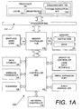
Figure 1A is a block diagram of a computer system formed with a processor that includes execution units to execute an instruction for shuffling data in accordance with one embodiment of the present invention; -
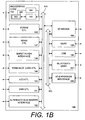
Figure 1B is a block diagram of another exemplary computer system in accordance with an alternative embodiment of the present invention; -
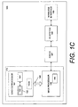
Figure 1C is a block diagram of yet another exemplary computer system in accordance with another alternative embodiment of the present invention; -
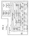
Figure 2 is a block diagram of the micro-architecture for a processor of one embodiment that includes logic circuits to perform data shuffle operations in accordance with the present invention; -
Figures 3A-C are illustrations of shuffle masks according to various embodiments of the present invention; -
Figure 4A is an illustration of various packed data type representations in multimedia registers according to one embodiment of the present invention; -
Figure 4B illustrates packed data-types in accordance with an alternative embodiment; -
Figure 4C illustrates one embodiment of an operation encoding (opcode) format for a shuffle instruction; -
Figure 4D illustrates an alternative operation encoding format; -
Figure 4E illustrates yet another alternative operation encoding format; -
Figure 5 is a block diagram of one embodiment of logic to perform a shuffle operation on a data operand based on a shuffle mask in accordance with the present invention; -
Figure 6 is a block diagram of one embodiment of a circuit for performing a data shuffling operation in accordance with the present invention; -
Figure 7 illustrates the operation of a data shuffle on byte wide data elements in accordance with one embodiment of the present invention; -
Figure 8 illustrates the operation of a data shuffle operation on word wide data elements in accordance with another embodiment of the present invention; -
Figure 9 is a flow chart illustrating one embodiment of a method to shuffle data; -
Figures 10A-H illustrate the operation of a parallel table lookup algorithm using SIMD instructions; -
Figure 11 is a flow chart illustrating one embodiment of a method to perform a table lookup using SIMD instructions; -
Figure 12 is a flow chart illustrating another embodiment of a method to perform a table lookup; -
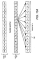
Figures 13A-C illustrates an algorithm for rearranging data between multiple registers; -
Figure 14 is a flow chart illustrating one embodiment of a method to rearrange data between multiple registers; -
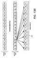
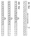
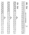
Figures 15A-K illustrates an algorithm for shuffling data between multiple registers to generate interleaved data; and -
Figure 16 is a flow chart illustrating one embodiment of a method to shuffle data between multiple registers to generate interleaved data. - A method and apparatus for shuffling data is disclosed. A method and apparatus for parallel table lookup using SIMD instructions are also described. A method and apparatus for rearranging data between multiple registers is also disclosed. The embodiments described herein are described in the context of a microprocessor, but are not so limited. Although the following embodiments are described with reference to a processor, other embodiments are applicable to other types of integrated circuits and logic devices. The same techniques and teachings of the present invention can easily be applied to other types of circuits or semiconductor devices that can benefit from higher pipeline throughput and improved performance. The teachings of the present invention are applicable to any processor or machine that performs data manipulations. However, the present invention is not limited to processors or machines that perform 256 bit, 128 bit, 64 bit, 32 bit, or 16 bit data operations and can be applied to any processor and machine in which shuffling of data is needed.
- In the following description, for purposes of explanation, numerous specific details are set forth in order to provide a thorough understanding of the present invention. One of ordinary skill in the art, however, will appreciate that these specific details are not necessary in order to practice the present invention. In other instances, well known electrical structures and circuits have not been set forth in particular detail in order to not necessarily obscure the present invention. In addition, the following description provides examples, and the accompanying drawings show various examples for the purposes of illustration. However, these examples should not be construed in a limiting sense as they are merely intended to provide examples of the present invention rather than to provide an exhaustive list of all possible implementations of the present invention.
- In an embodiment, the methods of the present invention are embodied in machine-executable instructions. The instructions can be used to cause a general-purpose or special-purpose processor that is programmed with the instructions to perform the steps of the present invention. Alternatively, the steps of the present invention might be performed by specific hardware components that contain hardwired logic for performing the steps, or by any combination of programmed computer components and custom hardware components.
- Although the below examples describe instruction handling and distribution in the context of execution units and logic circuits, other embodiments of the present invention can be accomplished by way of software. The present invention may be provided as a computer program product or software which may include a machine or computer-readable medium having stored thereon instructions which may be used to program a computer (or other electronic devices) to perform a process according to the present invention. Such software can be stored within a memory in the system. Similarly, the code can be distributed via a network or by way of other computer readable media. Thus a machine-readable medium may include any mechanism for storing or transmitting information in a form readable by a machine (e.g., a computer), but is not limited to, floppy diskettes, optical disks, Compact Disc, Read-Only Memory (CD-ROMs), and magneto-optical disks, Read-Only Memory (ROMs), Random Access Memory (RAM), Erasable Programmable Read-Only Memory (EPROM), Electrically Erasable Programmable Read-Only Memory (EEPROM), magnetic or optical cards, flash memory, a transmission over the Internet, electrical, optical, acoustical or other forms of propagated signals (e.g., carrier waves, infrared signals, digital signals, etc.) or the like.
- Accordingly, the computer-readable medium includes any type of media/machine-readable medium suitable for storing or transmitting electronic instructions or information in a form readable by a machine (e.g., a computer). Moreover, the present invention may also be downloaded as a computer program product. As such, the program may be transferred from a remote computer (e.g., a server) to a requesting computer (e.g., a client). The transfer of the program may be by way of electrical, optical, acoustical, or other forms of data signals embodied in a carrier wave or other propagation medium via a communication link (e.g., a modem, network connection or the like).
- Furthermore, embodiments of integrated circuit designs in accordance with the present inventions can be communicated or transferred in electronic form as a database on a tape or other machine readable media. For example, the electronic form of an integrated circuit design of a processor in one embodiment can be processed or manufactured via a fab to obtain a computer component. In another instance, an integrated circuit design in electronic form can be processed by a machine to simulate a computer component. Thus the circuit layout plans and/or designs of processors in some embodiments can be distributed via machine readable mediums or embodied thereon for fabrication into a circuit or for simulation of an integrated circuit which, when processed by a machine, simulates a processor. A machine readable medium is also capable of storing data representing predetermined functions in accordance with the present invention in other embodiments.
- In modem processors, a number of different execution units are used to process and execute a variety of code and instructions. Not all instructions are created equal as some are quicker to complete while others can take an enormous number of clock cycles. The faster the throughput of instructions, the better the overall performance of the processor. Thus it would be advantageous to have as many instructions execute as fast as possible. However, there are certain instructions that have greater complexity and require more in terms of execution time and processor resources. For example, there are floating point instructions, load/store operations, data moves, etc.
- As more and more computer systems are used in internet and multimedia applications, additional processor support has been introduced over time. For instance, Single Instruction, Multiple Data (SIMD) integer/floating point instructions and Streaming SIMD Extensions (SSE) are instructions that reduce the overall number of instructions required to execute a particular program task. These instructions can speed up software performance by operating on multiple data elements in parallel. As a result, performance gains can be achieved in a wide range of applications including video, speech, and image/photo processing. The implementation of SIMD instructions in microprocessors and similar types of logic circuit usually involve a number of issues. Furthermore, the complexity of SIMD operations often leads to a need for additional circuitry in order to correctly process and manipulate the data.
- Embodiments of the present invention provide a way to implement a packed byte shuffle instruction with a flush to zero capability as an algorithm that makes use of SIMD related hardware. For one embodiment, the algorithm is based on the concept of shuffling data from a particular register or memory location based on the values of a control mask for each data element position. Embodiments of a packed byte shuffle can be used to reduce the number of instructions required in many different applications that rearrange data. A packed byte shuffle instruction can also be used for any application with unaligned loads. Embodiments of this shuffle instruction can be used for filtering to arrange data for efficient multiply-accumulate operations. Similarly, a packed shuffle instruction can be used in video and encryption applications for ordering data and small lookup tables. This instruction can be used to mix data from two or more registers. Thus embodiments of a packed shuffle with a flush to zero capability algorithm in accordance with the present invention can be implemented in a processor to support SIMD operations efficiently without seriously compromising overall performance.
- Embodiments of the present invention provide a packed data shuffle instruction (PSHUFB) with a flush to zero capability for efficiently ordering and arranging data of any size. In one embodiment, data is shuffled or rearranged in a register with byte granularity. The byte shuffle operation orders data sizes, which are larger than bytes, by maintaining the relative position of bytes within the larger data during the shuffle operation. In addition, the byte shuffle operation can change the relative position of data in an SIMD register and can also duplicate data. This PSHUFB instruction shuffles bytes from a first source register in accordance to the contents of shuffle control bytes in a second source register. Although the instruction permutes the data, the shuffle mask is left unaffected and unchanged during this shuffle operation of this embodiment. The mnemonic for the one implementation is "
PSHUFB register 1, register 2 / memory", wherein the first and second operands are SIMD registers. However, the register of the second operand can also be replaced with a memory location. The first operand includes the source data for shuffling. For this embodiment, the register for the first operand is also the destination register. Embodiments in accordance to the present invention also include a capability of setting selected bytes to zero in addition to changing their position. - The second operand includes the set of shuffle control mask bytes to designate the shuffle pattern. The number of bits used to select a source data element is log2 of the number of data elements in the source operand. For instance, the number of bytes in a 128 bit register embodiment is sixteen. The log2 of sixteen is four. Thus four bits, or a nibble, is needed. The [3:0] index in the code below refers to the four bits. If the most significant bit (MSB),
bit 7 in this embodiment, of the shuffle control byte is set, a constant zero is written in the result byte. If the least significant nibble of byte I of the second operand, the mask set, contains the integer J, then the shuffle instruction causes the Jth byte of the first source register to be copied to the Ith byte position of the destination register. Below is example pseudo-code for one embodiment of a packed byte shuffle operation on 128 bit operands:
    For i = 0 to 15 {
        if (SRC2[(i*8)+7]=1)
             DEST[(i*8)+7...(i*8)+0] ← 0
        else
             index[3:0] ← SRC2[(i*8)+3 ... SRC2(i*8)+0]
             DEST[(i*8)+7...(i*8)+0] ← SRC1/DEST[(index*8+7)... (index*8+0)]
    }
    For i=0 to 7 {
        if (SRC2[(i * 8)+7] = 1)
             DEST[(i*8)+7...(i*8)+0] ← 0
        else
             index[2:0] ← SRC2[(i*8)+2 ... SRC2(i*8)+0]
             DEST[(i*8)+7...(i*8)+0] ← SRC1/DEST[(index*8+7)... (index*8+0)]
    }
Note that in this 64 bit register embodiment, the lower three bits of the mask are used as there are eight bytes in a 64 bit register. The log2 of eight is three. The [2:0] index in the code above refers to the three bits. In alternative embodiments, the number of bits in a mask can vary to accommodate the number of data elements available in the source data. For example, a mask with lower five bits is needed to select a data element in a 256 bit register.
- packed byte shuffle DATA A, MASK A;
- packed byte shuffle DATA B, MASK B;
- packed logical OR RESULTANT A, RESULTANT B.
Claims (39)
- A method comprising:receiving a first operand (510) having a set of L data elements and a second operand (520) having a set of L control elements; andfor each control element, shuffling data from a first operand (510) data element designated by said control element to an associated resultant (540) data element position if the flush to zero field of said each control element is not set and placing a zero into said associated resultant (540) data element position if said flush to zero field is set.
- The method of claim 1 wherein each of said L control elements occupies a particular position in said second operand (520) and is associated with a similarly located data element position in a resultant (540).
- The method of claim 2 wherein each of said L data elements occupies a particular position in said first operand (510).
- The method of claim 3 wherein said control element is to designate a first operand (510) data element by a data element position number.
- The method of claim 4 wherein each of said control elements is comprised of: a flush to zero field, said flush to zero field to indicate whether a data element position associated with this control element is to be filled with a zero value; and a selection field, said selection field to indicate which first operand data element to shuffle data from.
- The method of claim 5 wherein each of said control elements is further comprised of a source select field.
- The method of claim 2 further comprising outputting a resultant (540) data block comprising data that was shuffled from said first operand (510) in response to said control elements of said second operand (520).
- The method of claim 1 wherein each of said data elements comprises a byte of data.
- The method of claim 8 wherein each of said control elements is a byte wide.
- The method of claim 9 wherein L is 8 and wherein said first operand (510), said second operand (520), and said resultant (540) are each comprised of 64-bit wide packed data.
- The method of claim 9 wherein L is 16 and wherein said first operand (510), said second operand (520), and said resultant (540) are each comprised of 128-bit wide packed data.
- An apparatus comprising:an execution unit to execute a shuffle instruction including a first operand (510) comprised of a set of L data elements and a second operand (520) comprised of a set of L control elements, said shuffle instruction to cause said execution unit to:for each individual control element, determine whether its flush to zero field is set, and place a zero into an associated resultant data element position if true, otherwise shuffle data from a first operand (510) data element designated by said individual control element to said associated resultant (540) data element position.
- The apparatus of claim 12 wherein each of said L control elements occupies a position in said second operand (520) and is associated with a similarly located data element position in a resultant (540).
- The apparatus of claim 13 wherein each individual control element is to designate a first operand (510) data element by a data element position number.
- The apparatus of claim 14 wherein each of said control elements is comprised of: a flush to zero field, said flush to zero field to indicate whether a data element position associated with this control element is to be filled with a zero value; and a selection field, said selection field to indicate which first operand (510) data element to shuffle data from.
- The apparatus of claim 15 wherein each of said control elements is further comprised of a source select field.
- The apparatus of claim 16 wherein said shuffle instruction is to further cause said execution unit to generate a resultant having L data element positions that have been filled based on said set of L control elements.
- The apparatus of claim 12 wherein each of said data elements comprises a byte of data and each of said control elements is a byte wide.
- The apparatus of claim 18 wherein L is 8 wherein said first operand (510), said second operand (520), and said resultant (540) are each comprised of 64-bit wide packed data.
- The apparatus of claim 18 wherein L is 16 and wherein said first operand (510), said second operand (520), and said resultant (540) are each comprised of 128-bit wide packed data.
- A machine readable medium comprising program code means arranged to perform all the steps of the method as claimed in any of claims 1-11, 24, and 25 when that program code means is run on a computer.
- The machine readable medium of claim 21 wherein said data stored by said machine readable medium represents an integrated circuit design, which when fabricated performs said predetermined function in response to a single instruction.
- The machine readable medium of claim 21 wherein said program code means of said machine readable medium represents a computer instruction, which, if executed by a machine, causes said machine to perform said predetermined function.
- The method of claim 1 wherein the set of L control elements are a set of L masks, wherein each of said L masks occupies a particular position in said second operand (520) and is associated with a similarly located data element position in a resultant (540), each of said L masks to include the flush to zero field, further comprising:for each mask, determining whether its flush to zero field is set, and placing a zero into an associated resultant (540) data element position if true; andif its flush to zero field is not set, shuffling data from a first operand (510) data element designated by said mask to said associated resultant (540) data element position.
- The method of claim 1 wherein the set ofL control elements are a set of L shuffle masks, wherein each of said L shuffle masks associated with a similarly located data element position in a resultant (540), further comprising:for each individual shuffle mask, determining whether its flush to zero field is set, and placing a zero into an associated resultant (540) data element position if true, otherwise shuffling data from a first operand (510) data element designated by said individual shuffle mask to said associated resultant (540) data element position.
- The apparatus of claim 12, further comprising:a first memory location to store a plurality of source data elements;a second memory location to store a plurality of control elements, each of said control elements to correspond to a resultant data element position, and each of said control elements to include a flush to zero field and a selection field;control logic coupled to said second memory location, said control logic in response to values of said control elements to generate a plurality of selection signals and a plurality of flush to zero signals;a first plurality of multiplexers coupled to said first memory location and said plurality of selection signals, each of said first plurality of multiplexers to shuffle a data element for a specific resultant data element position in response to a selection signal corresponding to said specific resultant data element position; anda second plurality of multiplexers coupled to said first plurality of multiplexers and to said plurality of flush to zero signals, each of said second plurality of multiplexers associated with a specific resultant data element position, each of said second plurality of multiplexers to output a zero if its flush to zero signal is active or to output a data element shuffled for that specific resultant data element position.
- The apparatus of claim 26 wherein said plurality of source data elements is a first packed data operand (510).
- The apparatus of claim 27 where said plurality of control elements is a second packed data operand (520).
- The apparatus of claim 27 wherein said first and second memory locations are a single instruction multiple data registers.
- The apparatus of claim 29 wherein: said first packed operand (510) is 64 bits long and each of said source data elements is a byte wide; and said second packed operand (520) is 64 bits long and each of said control elements is a byte wide.
- The apparatus of claim 29 wherein: said first packed operand (510) is 128 bits long and each of said source data elements is a byte wide; and said second packed operand (520) is 128 bits long and each of said control elements is a byte wide.
- The apparatus of claim 12, further comprising:control logic to receive a set of L shuffle masks, wherein each shuffle mask is associated with a unique resultant data element position, said control logic to provide a select signal and a flush to zero signal for each resultant data element position;a set of L multiplexers coupled to said control logic, wherein each multiplexer is also associated with a unique resultant data element position, each multiplexer to output a zero if its associated flush to zero signal is active and to output data shuffled from a set of M data elements based on its associated select signal if its associated flush to zero signal is inactive.
- The apparatus of claim 32 further comprising a register with L unique data element positions, each data element position to hold an output from its associated multiplexer.
- The apparatus of claim 33 wherein L is 16 and M is 16.
- The apparatus of claim 12, further comprising:a memory (120) to store data and instructions;a processor (102) coupled to said memory on a bus (110), said processor (102) operable to perform a shuffle operation, said processor (102) comprising:a bus unit to receive an instruction from said memory (120), said instruction to cause a data shuffle on at least one of L data elements from a first operand (510) based on a set of L shuffle control elements from a second operand (520); whereinthe execution unit (108) is coupled to said bus unit.
- The system of claim 35 wherein said instruction is a packed byte shuffle instruction with flush to zero capability.
- The system of claim 35 wherein each data element is a byte wide, each shuffle command element is a byte wide, and L is 8.
- The system of claim 35 wherein said first operand (510) is 64 bits long and said second operand is 64 bits long.
- The method of claim 1, wherein the receiving the first operand (510), receiving the second operand (520), and placing data into an associated resultant (540) data element are performed in response to receiving a single packed shuffle instruction that designates, with 3 bits, a first register storing the first operand (510) and designates, with 3 bits, a second register storing the second operand (520), the first operand (510) and second operand (520) are of a same size and each of the L data elements and L shuffle masks are of a same size, and wherein each one of the L shuffle masks is divided into three portions, the first portion being a flush to zero bit occupying the most significant bit of each shuffle mask, the second portion being a position selection field that is at least log2L bits wide and indicates a position of one of said L data elements, and a third portion.
Applications Claiming Priority (2)
| Application Number | Priority Date | Filing Date | Title |
|---|---|---|---|
| US10/611,344 US20040054877A1 (en) | 2001-10-29 | 2003-06-30 | Method and apparatus for shuffling data |
| PCT/US2004/020601 WO2005006183A2 (en) | 2003-06-30 | 2004-06-24 | Method and apparatus for shuffling data |
Publications (2)
| Publication Number | Publication Date |
|---|---|
| EP1639452A2 EP1639452A2 (en) | 2006-03-29 |
| EP1639452B1 true EP1639452B1 (en) | 2009-09-09 |
Family
ID=34062338
Family Applications (1)
| Application Number | Title | Priority Date | Filing Date |
|---|---|---|---|
| EP04756204A Active EP1639452B1 (en) | 2003-06-30 | 2004-06-24 | Method and apparatus for shuffling data |
Country Status (11)
| Country | Link |
|---|---|
| US (8) | US20040054877A1 (en) |
| EP (1) | EP1639452B1 (en) |
| JP (4) | JP4607105B2 (en) |
| KR (1) | KR100831472B1 (en) |
| CN (2) | CN101620525B (en) |
| AT (1) | ATE442624T1 (en) |
| DE (1) | DE602004023081D1 (en) |
| HK (1) | HK1083657A1 (en) |
| RU (1) | RU2316808C2 (en) |
| TW (1) | TWI270007B (en) |
| WO (1) | WO2005006183A2 (en) |
Families Citing this family (115)
| Publication number | Priority date | Publication date | Assignee | Title |
|---|---|---|---|---|
| US20040054877A1 (en) | 2001-10-29 | 2004-03-18 | Macy William W. | Method and apparatus for shuffling data |
| US7739319B2 (en) * | 2001-10-29 | 2010-06-15 | Intel Corporation | Method and apparatus for parallel table lookup using SIMD instructions |
| US7925891B2 (en) * | 2003-04-18 | 2011-04-12 | Via Technologies, Inc. | Apparatus and method for employing cryptographic functions to generate a message digest |
| US7647557B2 (en) * | 2005-06-29 | 2010-01-12 | Intel Corporation | Techniques for shuffling video information |
| US7971042B2 (en) * | 2005-09-28 | 2011-06-28 | Synopsys, Inc. | Microprocessor system and method for instruction-initiated recording and execution of instruction sequences in a dynamically decoupleable extended instruction pipeline |
| US20070106883A1 (en) * | 2005-11-07 | 2007-05-10 | Choquette Jack H | Efficient Streaming of Un-Aligned Load/Store Instructions that Save Unused Non-Aligned Data in a Scratch Register for the Next Instruction |
| US20070226469A1 (en) * | 2006-03-06 | 2007-09-27 | James Wilson | Permutable address processor and method |
| US8290095B2 (en) | 2006-03-23 | 2012-10-16 | Qualcomm Incorporated | Viterbi pack instruction |
| US20080071851A1 (en) * | 2006-09-20 | 2008-03-20 | Ronen Zohar | Instruction and logic for performing a dot-product operation |
| US20080077772A1 (en) * | 2006-09-22 | 2008-03-27 | Ronen Zohar | Method and apparatus for performing select operations |
| US9069547B2 (en) * | 2006-09-22 | 2015-06-30 | Intel Corporation | Instruction and logic for processing text strings |
| US7536532B2 (en) * | 2006-09-27 | 2009-05-19 | International Business Machines Corporation | Merge operations of data arrays based on SIMD instructions |
| JP4686435B2 (en) * | 2006-10-27 | 2011-05-25 | 株式会社東芝 | Arithmetic unit |
| US7962718B2 (en) * | 2007-10-12 | 2011-06-14 | Freescale Semiconductor, Inc. | Methods for performing extended table lookups using SIMD vector permutation instructions that support out-of-range index values |
| US8700884B2 (en) * | 2007-10-12 | 2014-04-15 | Freescale Semiconductor, Inc. | Single-instruction multiple-data vector permutation instruction and method for performing table lookups for in-range index values and determining constant values for out-of-range index values |
| US8515052B2 (en) | 2007-12-17 | 2013-08-20 | Wai Wu | Parallel signal processing system and method |
| US8078836B2 (en) | 2007-12-30 | 2011-12-13 | Intel Corporation | Vector shuffle instructions operating on multiple lanes each having a plurality of data elements using a common set of per-lane control bits |
| GB2456775B (en) * | 2008-01-22 | 2012-10-31 | Advanced Risc Mach Ltd | Apparatus and method for performing permutation operations on data |
| US9513905B2 (en) | 2008-03-28 | 2016-12-06 | Intel Corporation | Vector instructions to enable efficient synchronization and parallel reduction operations |
| WO2009144681A1 (en) * | 2008-05-30 | 2009-12-03 | Nxp B.V. | Vector shuffle with write enable |
| US8195921B2 (en) * | 2008-07-09 | 2012-06-05 | Oracle America, Inc. | Method and apparatus for decoding multithreaded instructions of a microprocessor |
| JP5375114B2 (en) * | 2009-01-16 | 2013-12-25 | 富士通株式会社 | Processor |
| JP5438551B2 (en) * | 2009-04-23 | 2014-03-12 | 新日鉄住金ソリューションズ株式会社 | Information processing apparatus, information processing method, and program |
| US9507670B2 (en) * | 2010-06-14 | 2016-11-29 | Veeam Software Ag | Selective processing of file system objects for image level backups |
| EP2691850B1 (en) * | 2011-03-30 | 2018-05-16 | NXP USA, Inc. | Integrated circuit device and methods of performing bit manipulation therefor |
| US20120254588A1 (en) * | 2011-04-01 | 2012-10-04 | Jesus Corbal San Adrian | Systems, apparatuses, and methods for blending two source operands into a single destination using a writemask |
| US20120278591A1 (en) * | 2011-04-27 | 2012-11-01 | Advanced Micro Devices, Inc. | Crossbar switch module having data movement instruction processor module and methods for implementing the same |
| KR101918464B1 (en) | 2011-09-14 | 2018-11-15 | 삼성전자 주식회사 | A processor and a swizzle pattern providing apparatus based on a swizzled virtual register |
| WO2013057872A1 (en) * | 2011-10-18 | 2013-04-25 | パナソニック株式会社 | Shuffle pattern generating circuit, processor, shuffle pattern generating method, and instruction |
| WO2013089750A1 (en) * | 2011-12-15 | 2013-06-20 | Intel Corporation | Methods to optimize a program loop via vector instructions using a shuffle table and a blend table |
| CN104011646B (en) | 2011-12-22 | 2018-03-27 | 英特尔公司 | For processor, method, system and the instruction of the sequence for producing the continuous integral number according to numerical order |
| US10223112B2 (en) | 2011-12-22 | 2019-03-05 | Intel Corporation | Processors, methods, systems, and instructions to generate sequences of integers in which integers in consecutive positions differ by a constant integer stride and where a smallest integer is offset from zero by an integer offset |
| CN108681465B (en) * | 2011-12-22 | 2022-08-02 | 英特尔公司 | Processor, processor core and system for generating integer sequence |
| CN104011644B (en) | 2011-12-22 | 2017-12-08 | 英特尔公司 | Processor, method, system and instruction for generation according to the sequence of the integer of the phase difference constant span of numerical order |
| WO2013095541A1 (en) * | 2011-12-22 | 2013-06-27 | Intel Corporation | Apparatus and method for performing a permute operation |
| WO2013095611A1 (en) * | 2011-12-23 | 2013-06-27 | Intel Corporation | Apparatus and method for performing a permute operation |
| WO2013095610A1 (en) * | 2011-12-23 | 2013-06-27 | Intel Corporation | Apparatus and method for shuffling floating point or integer values |
| WO2013095657A1 (en) * | 2011-12-23 | 2013-06-27 | Intel Corporation | Instruction and logic to provide vector blend and permute functionality |
| JP5935319B2 (en) * | 2011-12-26 | 2016-06-15 | 富士通株式会社 | Circuit emulation apparatus, circuit emulation method, and circuit emulation program |
| US8683296B2 (en) | 2011-12-30 | 2014-03-25 | Streamscale, Inc. | Accelerated erasure coding system and method |
| US8914706B2 (en) | 2011-12-30 | 2014-12-16 | Streamscale, Inc. | Using parity data for concurrent data authentication, correction, compression, and encryption |
| US9329863B2 (en) | 2012-03-13 | 2016-05-03 | International Business Machines Corporation | Load register on condition with zero or immediate instruction |
| JP5730812B2 (en) * | 2012-05-02 | 2015-06-10 | 日本電信電話株式会社 | Arithmetic apparatus, method and program |
| US9268683B1 (en) * | 2012-05-14 | 2016-02-23 | Kandou Labs, S.A. | Storage method and apparatus for random access memory using codeword storage |
| US9953436B2 (en) | 2012-06-26 | 2018-04-24 | BTS Software Solutions, LLC | Low delay low complexity lossless compression system |
| WO2014004486A2 (en) * | 2012-06-26 | 2014-01-03 | Dunling Li | Low delay low complexity lossless compression system |
| US9218182B2 (en) * | 2012-06-29 | 2015-12-22 | Intel Corporation | Systems, apparatuses, and methods for performing a shuffle and operation (shuffle-op) |
| US9342479B2 (en) * | 2012-08-23 | 2016-05-17 | Qualcomm Incorporated | Systems and methods of data extraction in a vector processor |
| US9715385B2 (en) | 2013-01-23 | 2017-07-25 | International Business Machines Corporation | Vector exception code |
| US9778932B2 (en) * | 2013-01-23 | 2017-10-03 | International Business Machines Corporation | Vector generate mask instruction |
| US9471308B2 (en) | 2013-01-23 | 2016-10-18 | International Business Machines Corporation | Vector floating point test data class immediate instruction |
| US9513906B2 (en) | 2013-01-23 | 2016-12-06 | International Business Machines Corporation | Vector checksum instruction |
| US9823924B2 (en) | 2013-01-23 | 2017-11-21 | International Business Machines Corporation | Vector element rotate and insert under mask instruction |
| US9804840B2 (en) | 2013-01-23 | 2017-10-31 | International Business Machines Corporation | Vector Galois Field Multiply Sum and Accumulate instruction |
| US9207942B2 (en) * | 2013-03-15 | 2015-12-08 | Intel Corporation | Systems, apparatuses,and methods for zeroing of bits in a data element |
| US9405539B2 (en) * | 2013-07-31 | 2016-08-02 | Intel Corporation | Providing vector sub-byte decompression functionality |
| US11768689B2 (en) | 2013-08-08 | 2023-09-26 | Movidius Limited | Apparatus, systems, and methods for low power computational imaging |
| US10001993B2 (en) | 2013-08-08 | 2018-06-19 | Linear Algebra Technologies Limited | Variable-length instruction buffer management |
| CN103501348A (en) * | 2013-10-16 | 2014-01-08 | 华仪风能有限公司 | Communication method and system for master control system and monitoring system of wind generating set |
| US9582419B2 (en) * | 2013-10-25 | 2017-02-28 | Arm Limited | Data processing device and method for interleaved storage of data elements |
| KR102122406B1 (en) | 2013-11-06 | 2020-06-12 | 삼성전자주식회사 | Method and apparatus for processing shuffle instruction |
| US9880845B2 (en) * | 2013-11-15 | 2018-01-30 | Qualcomm Incorporated | Vector processing engines (VPEs) employing format conversion circuitry in data flow paths between vector data memory and execution units to provide in-flight format-converting of input vector data to execution units for vector processing operations, and related vector processor systems and methods |
| KR101898791B1 (en) * | 2013-12-23 | 2018-09-13 | 인텔 코포레이션 | Instruction and logic for identifying instructions for retirement in a multi-strand out-of-order processor |
| US9552209B2 (en) * | 2013-12-27 | 2017-01-24 | Intel Corporation | Functional unit for instruction execution pipeline capable of shifting different chunks of a packed data operand by different amounts |
| US9274835B2 (en) | 2014-01-06 | 2016-03-01 | International Business Machines Corporation | Data shuffling in a non-uniform memory access device |
| US9256534B2 (en) | 2014-01-06 | 2016-02-09 | International Business Machines Corporation | Data shuffling in a non-uniform memory access device |
| JP6374975B2 (en) * | 2014-03-27 | 2018-08-15 | インテル・コーポレーション | A processor, method, system, and instructions for storing successive source elements in a plurality of unmasked result elements and propagating to a plurality of masked result elements |
| CN106030514B (en) * | 2014-03-28 | 2022-09-13 | 英特尔公司 | Processor and method for executing masked source element store with propagation instructions |
| US9996579B2 (en) * | 2014-06-26 | 2018-06-12 | Amazon Technologies, Inc. | Fast color searching |
| US10169803B2 (en) | 2014-06-26 | 2019-01-01 | Amazon Technologies, Inc. | Color based social networking recommendations |
| US9424039B2 (en) * | 2014-07-09 | 2016-08-23 | Intel Corporation | Instruction for implementing vector loops of iterations having an iteration dependent condition |
| WO2016016726A2 (en) * | 2014-07-30 | 2016-02-04 | Linear Algebra Technologies Limited | Vector processor |
| US9619214B2 (en) | 2014-08-13 | 2017-04-11 | International Business Machines Corporation | Compiler optimizations for vector instructions |
| JP2017199045A (en) * | 2014-09-02 | 2017-11-02 | パナソニックIpマネジメント株式会社 | Processor and data sorting method |
| US9785649B1 (en) | 2014-09-02 | 2017-10-10 | Amazon Technologies, Inc. | Hue-based color naming for an image |
| US10133570B2 (en) | 2014-09-19 | 2018-11-20 | Intel Corporation | Processors, methods, systems, and instructions to select and consolidate active data elements in a register under mask into a least significant portion of result, and to indicate a number of data elements consolidated |
| EP3001307B1 (en) * | 2014-09-25 | 2019-11-13 | Intel Corporation | Bit shuffle processors, methods, systems, and instructions |
| US10169014B2 (en) | 2014-12-19 | 2019-01-01 | International Business Machines Corporation | Compiler method for generating instructions for vector operations in a multi-endian instruction set |
| US10296334B2 (en) * | 2014-12-27 | 2019-05-21 | Intel Corporation | Method and apparatus for performing a vector bit gather |
| US10296489B2 (en) | 2014-12-27 | 2019-05-21 | Intel Corporation | Method and apparatus for performing a vector bit shuffle |
| KR20160139823A (en) | 2015-05-28 | 2016-12-07 | 손규호 | Method of packing or unpacking that uses byte overlapping with two key numbers |
| US10001995B2 (en) * | 2015-06-02 | 2018-06-19 | Intel Corporation | Packed data alignment plus compute instructions, processors, methods, and systems |
| CN105022609A (en) * | 2015-08-05 | 2015-11-04 | 浪潮(北京)电子信息产业有限公司 | Data shuffling method and data shuffling unit |
| US9880821B2 (en) | 2015-08-17 | 2018-01-30 | International Business Machines Corporation | Compiler optimizations for vector operations that are reformatting-resistant |
| US10503502B2 (en) | 2015-09-25 | 2019-12-10 | Intel Corporation | Data element rearrangement, processors, methods, systems, and instructions |
| US10620957B2 (en) | 2015-10-22 | 2020-04-14 | Texas Instruments Incorporated | Method for forming constant extensions in the same execute packet in a VLIW processor |
| US9946541B2 (en) * | 2015-12-18 | 2018-04-17 | Intel Corporation | Systems, apparatuses, and method for strided access |
| US20170177350A1 (en) * | 2015-12-18 | 2017-06-22 | Intel Corporation | Instructions and Logic for Set-Multiple-Vector-Elements Operations |
| US10338920B2 (en) * | 2015-12-18 | 2019-07-02 | Intel Corporation | Instructions and logic for get-multiple-vector-elements operations |
| US20170177354A1 (en) * | 2015-12-18 | 2017-06-22 | Intel Corporation | Instructions and Logic for Vector-Based Bit Manipulation |
| US20170177351A1 (en) * | 2015-12-18 | 2017-06-22 | Intel Corporation | Instructions and Logic for Even and Odd Vector Get Operations |
| US10467006B2 (en) * | 2015-12-20 | 2019-11-05 | Intel Corporation | Permutating vector data scattered in a temporary destination into elements of a destination register based on a permutation factor |
| US10565207B2 (en) * | 2016-04-12 | 2020-02-18 | Hsilin Huang | Method, system and program product for mask-based compression of a sparse matrix |
| US10331830B1 (en) * | 2016-06-13 | 2019-06-25 | Apple Inc. | Heterogeneous logic gate simulation using SIMD instructions |
| US10592468B2 (en) * | 2016-07-13 | 2020-03-17 | Qualcomm Incorporated | Shuffler circuit for lane shuffle in SIMD architecture |
| US10169040B2 (en) * | 2016-11-16 | 2019-01-01 | Ceva D.S.P. Ltd. | System and method for sample rate conversion |
| CN106775587B (en) | 2016-11-30 | 2020-04-14 | 上海兆芯集成电路有限公司 | Method for executing computer instructions and device using same |
| EP3336692B1 (en) | 2016-12-13 | 2020-04-29 | Arm Ltd | Replicate partition instruction |
| EP3336691B1 (en) * | 2016-12-13 | 2022-04-06 | ARM Limited | Replicate elements instruction |
| US9959247B1 (en) | 2017-02-17 | 2018-05-01 | Google Llc | Permuting in a matrix-vector processor |
| US10140239B1 (en) | 2017-05-23 | 2018-11-27 | Texas Instruments Incorporated | Superimposing butterfly network controls for pattern combinations |
| US11194630B2 (en) | 2017-05-30 | 2021-12-07 | Microsoft Technology Licensing, Llc | Grouped shuffling of partition vertices |
| US10970081B2 (en) * | 2017-06-29 | 2021-04-06 | Advanced Micro Devices, Inc. | Stream processor with decoupled crossbar for cross lane operations |
| CN109324981B (en) * | 2017-07-31 | 2023-08-15 | 伊姆西Ip控股有限责任公司 | Cache management system and method |
| US10460416B1 (en) * | 2017-10-17 | 2019-10-29 | Xilinx, Inc. | Inline image preprocessing for convolution operations using a matrix multiplier on an integrated circuit |
| US10956125B2 (en) | 2017-12-21 | 2021-03-23 | International Business Machines Corporation | Data shuffling with hierarchical tuple spaces |
| US10891274B2 (en) | 2017-12-21 | 2021-01-12 | International Business Machines Corporation | Data shuffling with hierarchical tuple spaces |
| US11789734B2 (en) * | 2018-08-30 | 2023-10-17 | Advanced Micro Devices, Inc. | Padded vectorization with compile time known masks |
| US10620958B1 (en) | 2018-12-03 | 2020-04-14 | Advanced Micro Devices, Inc. | Crossbar between clients and a cache |
| CN109783054B (en) * | 2018-12-20 | 2021-03-09 | 中国科学院计算技术研究所 | Butterfly operation processing method and system of RSFQ FFT processor |
| US11200239B2 (en) | 2020-04-24 | 2021-12-14 | International Business Machines Corporation | Processing multiple data sets to generate a merged location-based data set |
| KR102381644B1 (en) * | 2020-11-27 | 2022-04-01 | 한국전자기술연구원 | Data sorting method for fast two-dimensional FFT signal processing and SoC applying the same |
| US20220197974A1 (en) * | 2020-12-22 | 2022-06-23 | Intel Corporation | Processors, methods, systems, and instructions to select and store data elements from two source two-dimensional arrays indicated by permute control elements in a result two-dimensional array |
| CN114297138B (en) * | 2021-12-10 | 2023-12-26 | 龙芯中科技术股份有限公司 | Vector shuffling method, processor and electronic equipment |
| CN115061731B (en) * | 2022-06-23 | 2023-05-23 | 摩尔线程智能科技(北京)有限责任公司 | Shuffling circuit and method, chip and integrated circuit device |
Family Cites Families (84)
| Publication number | Priority date | Publication date | Assignee | Title |
|---|---|---|---|---|
| US3711692A (en) | 1971-03-15 | 1973-01-16 | Goodyear Aerospace Corp | Determination of number of ones in a data field by addition |
| US3723715A (en) | 1971-08-25 | 1973-03-27 | Ibm | Fast modulo threshold operator binary adder for multi-number additions |
| US4139899A (en) | 1976-10-18 | 1979-02-13 | Burroughs Corporation | Shift network having a mask generator and a rotator |
| US4161784A (en) | 1978-01-05 | 1979-07-17 | Honeywell Information Systems, Inc. | Microprogrammable floating point arithmetic unit capable of performing arithmetic operations on long and short operands |
| US4418383A (en) | 1980-06-30 | 1983-11-29 | International Business Machines Corporation | Data flow component for processor and microprocessor systems |
| US4393468A (en) | 1981-03-26 | 1983-07-12 | Advanced Micro Devices, Inc. | Bit slice microprogrammable processor for signal processing applications |
| JPS57209570A (en) | 1981-06-19 | 1982-12-22 | Fujitsu Ltd | Vector processing device |
| US4498177A (en) | 1982-08-30 | 1985-02-05 | Sperry Corporation | M Out of N code checker circuit |
| US4569016A (en) | 1983-06-30 | 1986-02-04 | International Business Machines Corporation | Mechanism for implementing one machine cycle executable mask and rotate instructions in a primitive instruction set computing system |
| US4707800A (en) | 1985-03-04 | 1987-11-17 | Raytheon Company | Adder/substractor for variable length numbers |
| JPS6297060A (en) | 1985-10-23 | 1987-05-06 | Mitsubishi Electric Corp | Digital signal processor |
| US4989168A (en) | 1987-11-30 | 1991-01-29 | Fujitsu Limited | Multiplying unit in a computer system, capable of population counting |
| US5019968A (en) | 1988-03-29 | 1991-05-28 | Yulan Wang | Three-dimensional vector processor |
| EP0363176B1 (en) | 1988-10-07 | 1996-02-14 | International Business Machines Corporation | Word organised data processors |
| US4903228A (en) | 1988-11-09 | 1990-02-20 | International Business Machines Corporation | Single cycle merge/logic unit |
| KR920007505B1 (en) | 1989-02-02 | 1992-09-04 | 정호선 | Multiplier by using neural network |
| US5081698A (en) | 1989-02-14 | 1992-01-14 | Intel Corporation | Method and apparatus for graphics display data manipulation |
| US5497497A (en) | 1989-11-03 | 1996-03-05 | Compaq Computer Corp. | Method and apparatus for resetting multiple processors using a common ROM |
| US5168571A (en) | 1990-01-24 | 1992-12-01 | International Business Machines Corporation | System for aligning bytes of variable multi-bytes length operand based on alu byte length and a number of unprocessed byte data |
| FR2666472B1 (en) | 1990-08-31 | 1992-10-16 | Alcatel Nv | TEMPORARY INFORMATION STORAGE SYSTEM INCLUDING A BUFFER MEMORY RECORDING DATA IN FIXED OR VARIABLE LENGTH DATA BLOCKS. |
| US5268995A (en) | 1990-11-21 | 1993-12-07 | Motorola, Inc. | Method for executing graphics Z-compare and pixel merge instructions in a data processor |
| US5680161A (en) | 1991-04-03 | 1997-10-21 | Radius Inc. | Method and apparatus for high speed graphics data compression |
| US5187679A (en) | 1991-06-05 | 1993-02-16 | International Business Machines Corporation | Generalized 7/3 counters |
| US5321810A (en) | 1991-08-21 | 1994-06-14 | Digital Equipment Corporation | Address method for computer graphics system |
| US5423010A (en) | 1992-01-24 | 1995-06-06 | C-Cube Microsystems | Structure and method for packing and unpacking a stream of N-bit data to and from a stream of N-bit data words |
| JP2642039B2 (en) | 1992-05-22 | 1997-08-20 | インターナショナル・ビジネス・マシーンズ・コーポレイション | Array processor |
| US5426783A (en) | 1992-11-02 | 1995-06-20 | Amdahl Corporation | System for processing eight bytes or less by the move, pack and unpack instruction of the ESA/390 instruction set |
| US5408670A (en) | 1992-12-18 | 1995-04-18 | Xerox Corporation | Performing arithmetic in parallel on composite operands with packed multi-bit components |
| US5465374A (en) | 1993-01-12 | 1995-11-07 | International Business Machines Corporation | Processor for processing data string by byte-by-byte |
| US5568415A (en) | 1993-02-19 | 1996-10-22 | Digital Equipment Corporation | Content addressable memory having a pair of memory cells storing don't care states for address translation |
| US5524256A (en) | 1993-05-07 | 1996-06-04 | Apple Computer, Inc. | Method and system for reordering bytes in a data stream |
| JPH0721034A (en) | 1993-06-28 | 1995-01-24 | Fujitsu Ltd | Character string copying processing method |
| US5625374A (en) * | 1993-09-07 | 1997-04-29 | Apple Computer, Inc. | Method for parallel interpolation of images |
| US5390135A (en) | 1993-11-29 | 1995-02-14 | Hewlett-Packard | Parallel shift and add circuit and method |
| US5487159A (en) | 1993-12-23 | 1996-01-23 | Unisys Corporation | System for processing shift, mask, and merge operations in one instruction |
| US5399135A (en) | 1993-12-29 | 1995-03-21 | Azzouni; Paul | Forearm workout bar |
| US5781457A (en) | 1994-03-08 | 1998-07-14 | Exponential Technology, Inc. | Merge/mask, rotate/shift, and boolean operations from two instruction sets executed in a vectored mux on a dual-ALU |
| US5594437A (en) | 1994-08-01 | 1997-01-14 | Motorola, Inc. | Circuit and method of unpacking a serial bitstream |
| US5579253A (en) | 1994-09-02 | 1996-11-26 | Lee; Ruby B. | Computer multiply instruction with a subresult selection option |
| US6275834B1 (en) | 1994-12-01 | 2001-08-14 | Intel Corporation | Apparatus for performing packed shift operations |
| US5819101A (en) | 1994-12-02 | 1998-10-06 | Intel Corporation | Method for packing a plurality of packed data elements in response to a pack instruction |
| US5636352A (en) | 1994-12-16 | 1997-06-03 | International Business Machines Corporation | Method and apparatus for utilizing condensed instructions |
| TW388982B (en) | 1995-03-31 | 2000-05-01 | Samsung Electronics Co Ltd | Memory controller which executes read and write commands out of order |
| GB9509989D0 (en) | 1995-05-17 | 1995-07-12 | Sgs Thomson Microelectronics | Manipulation of data |
| US6381690B1 (en) | 1995-08-01 | 2002-04-30 | Hewlett-Packard Company | Processor for performing subword permutations and combinations |
| US7085795B2 (en) * | 2001-10-29 | 2006-08-01 | Intel Corporation | Apparatus and method for efficient filtering and convolution of content data |
| CN103092564B (en) | 1995-08-31 | 2016-04-06 | 英特尔公司 | Perform the processor taken advantage of and add instruction and system integrated data execution being taken advantage of to add operation |
| US5819117A (en) | 1995-10-10 | 1998-10-06 | Microunity Systems Engineering, Inc. | Method and system for facilitating byte ordering interfacing of a computer system |
| US5838984A (en) | 1996-08-19 | 1998-11-17 | Samsung Electronics Co., Ltd. | Single-instruction-multiple-data processing using multiple banks of vector registers |
| US5909572A (en) | 1996-12-02 | 1999-06-01 | Compaq Computer Corp. | System and method for conditionally moving an operand from a source register to a destination register |
| US6061521A (en) * | 1996-12-02 | 2000-05-09 | Compaq Computer Corp. | Computer having multimedia operations executable as two distinct sets of operations within a single instruction cycle |
| DE19654846A1 (en) | 1996-12-27 | 1998-07-09 | Pact Inf Tech Gmbh | Process for the independent dynamic reloading of data flow processors (DFPs) as well as modules with two- or multi-dimensional programmable cell structures (FPGAs, DPGAs, etc.) |
| US5933650A (en) | 1997-10-09 | 1999-08-03 | Mips Technologies, Inc. | Alignment and ordering of vector elements for single instruction multiple data processing |
| US6223277B1 (en) | 1997-11-21 | 2001-04-24 | Texas Instruments Incorporated | Data processing circuit with packed data structure capability |
| US6307553B1 (en) | 1998-03-31 | 2001-10-23 | Mohammad Abdallah | System and method for performing a MOVHPS-MOVLPS instruction |
| US6122725A (en) * | 1998-03-31 | 2000-09-19 | Intel Corporation | Executing partial-width packed data instructions |
| US6192467B1 (en) | 1998-03-31 | 2001-02-20 | Intel Corporation | Executing partial-width packed data instructions |
| US6041404A (en) | 1998-03-31 | 2000-03-21 | Intel Corporation | Dual function system and method for shuffling packed data elements |
| US6211892B1 (en) | 1998-03-31 | 2001-04-03 | Intel Corporation | System and method for performing an intra-add operation |
| US6115812A (en) | 1998-04-01 | 2000-09-05 | Intel Corporation | Method and apparatus for efficient vertical SIMD computations |
| US6288723B1 (en) | 1998-04-01 | 2001-09-11 | Intel Corporation | Method and apparatus for converting data format to a graphics card |
| US5996057A (en) * | 1998-04-17 | 1999-11-30 | Apple | Data processing system and method of permutation with replication within a vector register file |
| US6098087A (en) | 1998-04-23 | 2000-08-01 | Infineon Technologies North America Corp. | Method and apparatus for performing shift operations on packed data |
| US6263426B1 (en) | 1998-04-30 | 2001-07-17 | Intel Corporation | Conversion from packed floating point data to packed 8-bit integer data in different architectural registers |
| JP3869947B2 (en) * | 1998-08-04 | 2007-01-17 | 株式会社日立製作所 | Parallel processing processor and parallel processing method |
| US20020002666A1 (en) * | 1998-10-12 | 2002-01-03 | Carole Dulong | Conditional operand selection using mask operations |
| US6405300B1 (en) * | 1999-03-22 | 2002-06-11 | Sun Microsystems, Inc. | Combining results of selectively executed remaining sub-instructions with that of emulated sub-instruction causing exception in VLIW processor |
| US6484255B1 (en) | 1999-09-20 | 2002-11-19 | Intel Corporation | Selective writing of data elements from packed data based upon a mask using predication |
| US6446198B1 (en) | 1999-09-30 | 2002-09-03 | Apple Computer, Inc. | Vectorized table lookup |
| US6546480B1 (en) | 1999-10-01 | 2003-04-08 | Hitachi, Ltd. | Instructions for arithmetic operations on vectored data |
| US20050188182A1 (en) * | 1999-12-30 | 2005-08-25 | Texas Instruments Incorporated | Microprocessor having a set of byte intermingling instructions |
| US6745319B1 (en) | 2000-02-18 | 2004-06-01 | Texas Instruments Incorporated | Microprocessor with instructions for shuffling and dealing data |
| EP1261912A2 (en) * | 2000-03-08 | 2002-12-04 | Sun Microsystems, Inc. | Processing architecture having sub-word shuffling and opcode modification |
| WO2001069938A1 (en) | 2000-03-15 | 2001-09-20 | Digital Accelerator Corporation | Coding of digital video with high motion content |
| US7155601B2 (en) | 2001-02-14 | 2006-12-26 | Intel Corporation | Multi-element operand sub-portion shuffle instruction execution |
| KR100446235B1 (en) | 2001-05-07 | 2004-08-30 | 엘지전자 주식회사 | Merging search method of motion vector using multi-candidates |
| US7162607B2 (en) * | 2001-08-31 | 2007-01-09 | Intel Corporation | Apparatus and method for a data storage device with a plurality of randomly located data |
| US20040054877A1 (en) | 2001-10-29 | 2004-03-18 | Macy William W. | Method and apparatus for shuffling data |
| US7739319B2 (en) | 2001-10-29 | 2010-06-15 | Intel Corporation | Method and apparatus for parallel table lookup using SIMD instructions |
| US7631025B2 (en) * | 2001-10-29 | 2009-12-08 | Intel Corporation | Method and apparatus for rearranging data between multiple registers |
| US7272622B2 (en) | 2001-10-29 | 2007-09-18 | Intel Corporation | Method and apparatus for parallel shift right merge of data |
| US7685212B2 (en) | 2001-10-29 | 2010-03-23 | Intel Corporation | Fast full search motion estimation with SIMD merge instruction |
| US7343389B2 (en) * | 2002-05-02 | 2008-03-11 | Intel Corporation | Apparatus and method for SIMD modular multiplication |
| US6914938B2 (en) | 2002-06-18 | 2005-07-05 | Motorola, Inc. | Interlaced video motion estimation |
-
2003
- 2003-06-30 US US10/611,344 patent/US20040054877A1/en not_active Abandoned
-
2004
- 2004-06-24 RU RU2006102503A patent/RU2316808C2/en active
- 2004-06-24 EP EP04756204A patent/EP1639452B1/en active Active
- 2004-06-24 CN CN200910130582.4A patent/CN101620525B/en active Active
- 2004-06-24 JP JP2006515370A patent/JP4607105B2/en active Active
- 2004-06-24 AT AT04756204T patent/ATE442624T1/en not_active IP Right Cessation
- 2004-06-24 WO PCT/US2004/020601 patent/WO2005006183A2/en active Application Filing
- 2004-06-24 CN CNB2004800184438A patent/CN100492278C/en active Active
- 2004-06-24 DE DE602004023081T patent/DE602004023081D1/en active Active
- 2004-06-24 KR KR20057025313A patent/KR100831472B1/en active IP Right Grant
- 2004-06-28 TW TW93118830A patent/TWI270007B/en not_active IP Right Cessation
-
2006
- 2006-05-18 HK HK06105784.3A patent/HK1083657A1/en not_active IP Right Cessation
-
2009
- 2009-03-31 US US12/387,958 patent/US8214626B2/en not_active Expired - Lifetime
-
2010
- 2010-08-11 JP JP2010180413A patent/JP5490645B2/en active Active
- 2010-10-08 US US12/901,336 patent/US8225075B2/en not_active Expired - Lifetime
-
2011
- 2011-03-02 JP JP2011045001A patent/JP5535965B2/en active Active
-
2012
- 2012-07-02 US US13/540,576 patent/US9477472B2/en not_active Expired - Lifetime
- 2012-09-10 US US13/608,953 patent/US8688959B2/en not_active Expired - Lifetime
-
2013
- 2013-05-31 JP JP2013115254A patent/JP5567181B2/en active Active
-
2014
- 2014-12-30 US US14/586,581 patent/US9229719B2/en not_active Expired - Fee Related
- 2014-12-30 US US14/586,558 patent/US9229718B2/en not_active Expired - Fee Related
-
2016
- 2016-10-21 US US15/299,914 patent/US10152323B2/en not_active Expired - Fee Related
Also Published As
Similar Documents
| Publication | Publication Date | Title |
|---|---|---|
| US10152323B2 (en) | Method and apparatus for shuffling data | |
| US7739319B2 (en) | Method and apparatus for parallel table lookup using SIMD instructions | |
| US7631025B2 (en) | Method and apparatus for rearranging data between multiple registers | |
| US11023236B2 (en) | Instruction and logic for processing text strings | |
| US8745358B2 (en) | Processor to execute shift right merge instructions | |
| US20130290392A1 (en) | Instruction and logic for performing a dot-product operation |
Legal Events
| Date | Code | Title | Description |
|---|---|---|---|
| PUAI | Public reference made under article 153(3) epc to a published international application that has entered the european phase |
Free format text: ORIGINAL CODE: 0009012 |
|
| 17P | Request for examination filed |
Effective date: 20051024 |
|
| AK | Designated contracting states |
Kind code of ref document: A2 Designated state(s): AT BE BG CH CY CZ DE DK EE ES FI FR GB GR HU IE IT LI LU MC NL PL PT RO SE SI SK TR |
|
| AX | Request for extension of the european patent |
Extension state: AL HR LT LV MK |
|
| REG | Reference to a national code |
Ref country code: HK Ref legal event code: DE Ref document number: 1083657 Country of ref document: HK |
|
| DAX | Request for extension of the european patent (deleted) | ||
| RIN1 | Information on inventor provided before grant (corrected) |
Inventor name: MACY, WILLIAM, JR. Inventor name: DEBES, ERIC Inventor name: NGUYEN, HUY Inventor name: ROUSSEL, PATRICE |
|
| 17Q | First examination report despatched |
Effective date: 20070718 |
|
| GRAP | Despatch of communication of intention to grant a patent |
Free format text: ORIGINAL CODE: EPIDOSNIGR1 |
|
| GRAS | Grant fee paid |
Free format text: ORIGINAL CODE: EPIDOSNIGR3 |
|
| GRAA | (expected) grant |
Free format text: ORIGINAL CODE: 0009210 |
|
| AK | Designated contracting states |
Kind code of ref document: B1 Designated state(s): AT BE BG CH CY CZ DE DK EE ES FI FR GB GR HU IE IT LI LU MC NL PL PT RO SE SI SK TR |
|
| REG | Reference to a national code |
Ref country code: GB Ref legal event code: FG4D |
|
| REG | Reference to a national code |
Ref country code: CH Ref legal event code: EP |
|
| REG | Reference to a national code |
Ref country code: IE Ref legal event code: FG4D |
|
| REF | Corresponds to: |
Ref document number: 602004023081 Country of ref document: DE Date of ref document: 20091022 Kind code of ref document: P |
|
| REG | Reference to a national code |
Ref country code: HK Ref legal event code: GR Ref document number: 1083657 Country of ref document: HK |
|
| PG25 | Lapsed in a contracting state [announced via postgrant information from national office to epo] |
Ref country code: FI Free format text: LAPSE BECAUSE OF FAILURE TO SUBMIT A TRANSLATION OF THE DESCRIPTION OR TO PAY THE FEE WITHIN THE PRESCRIBED TIME-LIMIT Effective date: 20090909 Ref country code: SE Free format text: LAPSE BECAUSE OF FAILURE TO SUBMIT A TRANSLATION OF THE DESCRIPTION OR TO PAY THE FEE WITHIN THE PRESCRIBED TIME-LIMIT Effective date: 20090909 |
|
| NLV1 | Nl: lapsed or annulled due to failure to fulfill the requirements of art. 29p and 29m of the patents act | ||
| PG25 | Lapsed in a contracting state [announced via postgrant information from national office to epo] |
Ref country code: SI Free format text: LAPSE BECAUSE OF FAILURE TO SUBMIT A TRANSLATION OF THE DESCRIPTION OR TO PAY THE FEE WITHIN THE PRESCRIBED TIME-LIMIT Effective date: 20090909 Ref country code: NL Free format text: LAPSE BECAUSE OF FAILURE TO SUBMIT A TRANSLATION OF THE DESCRIPTION OR TO PAY THE FEE WITHIN THE PRESCRIBED TIME-LIMIT Effective date: 20090909 Ref country code: PL Free format text: LAPSE BECAUSE OF FAILURE TO SUBMIT A TRANSLATION OF THE DESCRIPTION OR TO PAY THE FEE WITHIN THE PRESCRIBED TIME-LIMIT Effective date: 20090909 |
|
| PG25 | Lapsed in a contracting state [announced via postgrant information from national office to epo] |
Ref country code: CY Free format text: LAPSE BECAUSE OF FAILURE TO SUBMIT A TRANSLATION OF THE DESCRIPTION OR TO PAY THE FEE WITHIN THE PRESCRIBED TIME-LIMIT Effective date: 20090909 |
|
| PG25 | Lapsed in a contracting state [announced via postgrant information from national office to epo] |
Ref country code: EE Free format text: LAPSE BECAUSE OF FAILURE TO SUBMIT A TRANSLATION OF THE DESCRIPTION OR TO PAY THE FEE WITHIN THE PRESCRIBED TIME-LIMIT Effective date: 20090909 Ref country code: RO Free format text: LAPSE BECAUSE OF FAILURE TO SUBMIT A TRANSLATION OF THE DESCRIPTION OR TO PAY THE FEE WITHIN THE PRESCRIBED TIME-LIMIT Effective date: 20090909 Ref country code: CZ Free format text: LAPSE BECAUSE OF FAILURE TO SUBMIT A TRANSLATION OF THE DESCRIPTION OR TO PAY THE FEE WITHIN THE PRESCRIBED TIME-LIMIT Effective date: 20090909 Ref country code: ES Free format text: LAPSE BECAUSE OF FAILURE TO SUBMIT A TRANSLATION OF THE DESCRIPTION OR TO PAY THE FEE WITHIN THE PRESCRIBED TIME-LIMIT Effective date: 20091220 Ref country code: PT Free format text: LAPSE BECAUSE OF FAILURE TO SUBMIT A TRANSLATION OF THE DESCRIPTION OR TO PAY THE FEE WITHIN THE PRESCRIBED TIME-LIMIT Effective date: 20100111 |
|
| PG25 | Lapsed in a contracting state [announced via postgrant information from national office to epo] |
Ref country code: SK Free format text: LAPSE BECAUSE OF FAILURE TO SUBMIT A TRANSLATION OF THE DESCRIPTION OR TO PAY THE FEE WITHIN THE PRESCRIBED TIME-LIMIT Effective date: 20090909 |
|
| PG25 | Lapsed in a contracting state [announced via postgrant information from national office to epo] |
Ref country code: AT Free format text: LAPSE BECAUSE OF FAILURE TO SUBMIT A TRANSLATION OF THE DESCRIPTION OR TO PAY THE FEE WITHIN THE PRESCRIBED TIME-LIMIT Effective date: 20090909 Ref country code: BE Free format text: LAPSE BECAUSE OF FAILURE TO SUBMIT A TRANSLATION OF THE DESCRIPTION OR TO PAY THE FEE WITHIN THE PRESCRIBED TIME-LIMIT Effective date: 20090909 |
|
| PLBE | No opposition filed within time limit |
Free format text: ORIGINAL CODE: 0009261 |
|
| STAA | Information on the status of an ep patent application or granted ep patent |
Free format text: STATUS: NO OPPOSITION FILED WITHIN TIME LIMIT |
|
| PG25 | Lapsed in a contracting state [announced via postgrant information from national office to epo] |
Ref country code: DK Free format text: LAPSE BECAUSE OF FAILURE TO SUBMIT A TRANSLATION OF THE DESCRIPTION OR TO PAY THE FEE WITHIN THE PRESCRIBED TIME-LIMIT Effective date: 20090909 |
|
| 26N | No opposition filed |
Effective date: 20100610 |
|
| PG25 | Lapsed in a contracting state [announced via postgrant information from national office to epo] |
Ref country code: GR Free format text: LAPSE BECAUSE OF FAILURE TO SUBMIT A TRANSLATION OF THE DESCRIPTION OR TO PAY THE FEE WITHIN THE PRESCRIBED TIME-LIMIT Effective date: 20091210 |
|
| PG25 | Lapsed in a contracting state [announced via postgrant information from national office to epo] |
Ref country code: MC Free format text: LAPSE BECAUSE OF NON-PAYMENT OF DUE FEES Effective date: 20100630 |
|
| REG | Reference to a national code |
Ref country code: CH Ref legal event code: PL |
|
| REG | Reference to a national code |
Ref country code: FR Ref legal event code: ST Effective date: 20110228 |
|
| PG25 | Lapsed in a contracting state [announced via postgrant information from national office to epo] |
Ref country code: IT Free format text: LAPSE BECAUSE OF FAILURE TO SUBMIT A TRANSLATION OF THE DESCRIPTION OR TO PAY THE FEE WITHIN THE PRESCRIBED TIME-LIMIT Effective date: 20090909 |
|
| PG25 | Lapsed in a contracting state [announced via postgrant information from national office to epo] |
Ref country code: IE Free format text: LAPSE BECAUSE OF NON-PAYMENT OF DUE FEES Effective date: 20100624 Ref country code: LI Free format text: LAPSE BECAUSE OF NON-PAYMENT OF DUE FEES Effective date: 20100630 Ref country code: CH Free format text: LAPSE BECAUSE OF NON-PAYMENT OF DUE FEES Effective date: 20100630 |
|
| PG25 | Lapsed in a contracting state [announced via postgrant information from national office to epo] |
Ref country code: FR Free format text: LAPSE BECAUSE OF NON-PAYMENT OF DUE FEES Effective date: 20100630 |
|
| PG25 | Lapsed in a contracting state [announced via postgrant information from national office to epo] |
Ref country code: HU Free format text: LAPSE BECAUSE OF FAILURE TO SUBMIT A TRANSLATION OF THE DESCRIPTION OR TO PAY THE FEE WITHIN THE PRESCRIBED TIME-LIMIT Effective date: 20100310 Ref country code: LU Free format text: LAPSE BECAUSE OF NON-PAYMENT OF DUE FEES Effective date: 20100624 Ref country code: BG Free format text: LAPSE BECAUSE OF FAILURE TO SUBMIT A TRANSLATION OF THE DESCRIPTION OR TO PAY THE FEE WITHIN THE PRESCRIBED TIME-LIMIT Effective date: 20090909 |
|
| PG25 | Lapsed in a contracting state [announced via postgrant information from national office to epo] |
Ref country code: TR Free format text: LAPSE BECAUSE OF FAILURE TO SUBMIT A TRANSLATION OF THE DESCRIPTION OR TO PAY THE FEE WITHIN THE PRESCRIBED TIME-LIMIT Effective date: 20090909 |
|
| PGFP | Annual fee paid to national office [announced via postgrant information from national office to epo] |
Ref country code: GB Payment date: 20220519 Year of fee payment: 19 |
|
| P01 | Opt-out of the competence of the unified patent court (upc) registered |
Effective date: 20230518 |
|
| PGFP | Annual fee paid to national office [announced via postgrant information from national office to epo] |
Ref country code: DE Payment date: 20230516 Year of fee payment: 20 |
|
| GBPC | Gb: european patent ceased through non-payment of renewal fee |
Effective date: 20230624 |