EP1617480A2 - Solid-state image sensor - Google Patents
Solid-state image sensor Download PDFInfo
- Publication number
- EP1617480A2 EP1617480A2 EP04257686A EP04257686A EP1617480A2 EP 1617480 A2 EP1617480 A2 EP 1617480A2 EP 04257686 A EP04257686 A EP 04257686A EP 04257686 A EP04257686 A EP 04257686A EP 1617480 A2 EP1617480 A2 EP 1617480A2
- Authority
- EP
- European Patent Office
- Prior art keywords
- well
- region
- image sensor
- solid
- state image
- Prior art date
- Legal status (The legal status is an assumption and is not a legal conclusion. Google has not performed a legal analysis and makes no representation as to the accuracy of the status listed.)
- Granted
Links
- 239000004065 semiconductor Substances 0.000 claims abstract description 102
- 239000000758 substrate Substances 0.000 claims abstract description 102
- 239000010410 layer Substances 0.000 description 134
- 229920002120 photoresistant polymer Polymers 0.000 description 86
- 238000000034 method Methods 0.000 description 85
- 239000012535 impurity Substances 0.000 description 66
- 238000009413 insulation Methods 0.000 description 47
- 239000002019 doping agent Substances 0.000 description 46
- 238000005468 ion implantation Methods 0.000 description 38
- VYPSYNLAJGMNEJ-UHFFFAOYSA-N Silicium dioxide Chemical compound O=[Si]=O VYPSYNLAJGMNEJ-UHFFFAOYSA-N 0.000 description 21
- 229910052814 silicon oxide Inorganic materials 0.000 description 21
- 230000001133 acceleration Effects 0.000 description 19
- 238000002955 isolation Methods 0.000 description 17
- 238000000206 photolithography Methods 0.000 description 16
- 238000004528 spin coating Methods 0.000 description 16
- 230000004048 modification Effects 0.000 description 15
- 238000012986 modification Methods 0.000 description 15
- 229910052751 metal Inorganic materials 0.000 description 14
- 239000002184 metal Substances 0.000 description 14
- 239000011229 interlayer Substances 0.000 description 11
- 229910021332 silicide Inorganic materials 0.000 description 10
- FVBUAEGBCNSCDD-UHFFFAOYSA-N silicide(4-) Chemical compound [Si-4] FVBUAEGBCNSCDD-UHFFFAOYSA-N 0.000 description 10
- ZOXJGFHDIHLPTG-UHFFFAOYSA-N Boron Chemical compound [B] ZOXJGFHDIHLPTG-UHFFFAOYSA-N 0.000 description 9
- 229910052796 boron Inorganic materials 0.000 description 9
- 229910052581 Si3N4 Inorganic materials 0.000 description 8
- HQVNEWCFYHHQES-UHFFFAOYSA-N silicon nitride Chemical compound N12[Si]34N5[Si]62N3[Si]51N64 HQVNEWCFYHHQES-UHFFFAOYSA-N 0.000 description 8
- 230000003647 oxidation Effects 0.000 description 7
- 238000007254 oxidation reaction Methods 0.000 description 7
- OAICVXFJPJFONN-UHFFFAOYSA-N Phosphorus Chemical compound [P] OAICVXFJPJFONN-UHFFFAOYSA-N 0.000 description 5
- 238000006243 chemical reaction Methods 0.000 description 5
- GUTLYIVDDKVIGB-UHFFFAOYSA-N cobalt atom Chemical compound [Co] GUTLYIVDDKVIGB-UHFFFAOYSA-N 0.000 description 5
- 230000001276 controlling effect Effects 0.000 description 5
- 230000002093 peripheral effect Effects 0.000 description 5
- 229910052698 phosphorus Inorganic materials 0.000 description 5
- 239000011574 phosphorus Substances 0.000 description 5
- NBIIXXVUZAFLBC-UHFFFAOYSA-N Phosphoric acid Chemical compound OP(O)(O)=O NBIIXXVUZAFLBC-UHFFFAOYSA-N 0.000 description 4
- XUIMIQQOPSSXEZ-UHFFFAOYSA-N Silicon Chemical compound [Si] XUIMIQQOPSSXEZ-UHFFFAOYSA-N 0.000 description 4
- 239000010941 cobalt Substances 0.000 description 4
- 229910017052 cobalt Inorganic materials 0.000 description 4
- 239000004020 conductor Substances 0.000 description 4
- 229910052782 aluminium Inorganic materials 0.000 description 3
- XAGFODPZIPBFFR-UHFFFAOYSA-N aluminium Chemical compound [Al] XAGFODPZIPBFFR-UHFFFAOYSA-N 0.000 description 3
- 239000012299 nitrogen atmosphere Substances 0.000 description 3
- 229910021420 polycrystalline silicon Inorganic materials 0.000 description 3
- 229920005591 polysilicon Polymers 0.000 description 3
- 229910052710 silicon Inorganic materials 0.000 description 3
- 239000010703 silicon Substances 0.000 description 3
- WFKWXMTUELFFGS-UHFFFAOYSA-N tungsten Chemical compound [W] WFKWXMTUELFFGS-UHFFFAOYSA-N 0.000 description 3
- 229910052721 tungsten Inorganic materials 0.000 description 3
- 239000010937 tungsten Substances 0.000 description 3
- KRHYYFGTRYWZRS-UHFFFAOYSA-N Fluorane Chemical compound F KRHYYFGTRYWZRS-UHFFFAOYSA-N 0.000 description 2
- 229910000147 aluminium phosphate Inorganic materials 0.000 description 2
- 229910052785 arsenic Inorganic materials 0.000 description 2
- RQNWIZPPADIBDY-UHFFFAOYSA-N arsenic atom Chemical compound [As] RQNWIZPPADIBDY-UHFFFAOYSA-N 0.000 description 2
- 239000012298 atmosphere Substances 0.000 description 2
- 239000011159 matrix material Substances 0.000 description 2
- RTAQQCXQSZGOHL-UHFFFAOYSA-N Titanium Chemical compound [Ti] RTAQQCXQSZGOHL-UHFFFAOYSA-N 0.000 description 1
- 230000003321 amplification Effects 0.000 description 1
- 239000011248 coating agent Substances 0.000 description 1
- 238000000576 coating method Methods 0.000 description 1
- 230000002596 correlated effect Effects 0.000 description 1
- 238000003199 nucleic acid amplification method Methods 0.000 description 1
- 238000005268 plasma chemical vapour deposition Methods 0.000 description 1
- 238000005070 sampling Methods 0.000 description 1
- 239000007787 solid Substances 0.000 description 1
- 238000004544 sputter deposition Methods 0.000 description 1
- 230000000087 stabilizing effect Effects 0.000 description 1
- 239000010936 titanium Substances 0.000 description 1
- 229910052719 titanium Inorganic materials 0.000 description 1
- 229910021341 titanium silicide Inorganic materials 0.000 description 1
Images


Classifications
-
- H—ELECTRICITY
- H01—ELECTRIC ELEMENTS
- H01L—SEMICONDUCTOR DEVICES NOT COVERED BY CLASS H10
- H01L27/00—Devices consisting of a plurality of semiconductor or other solid-state components formed in or on a common substrate
- H01L27/14—Devices consisting of a plurality of semiconductor or other solid-state components formed in or on a common substrate including semiconductor components sensitive to infrared radiation, light, electromagnetic radiation of shorter wavelength or corpuscular radiation and specially adapted either for the conversion of the energy of such radiation into electrical energy or for the control of electrical energy by such radiation
- H01L27/144—Devices controlled by radiation
- H01L27/146—Imager structures
- H01L27/14601—Structural or functional details thereof
- H01L27/14609—Pixel-elements with integrated switching, control, storage or amplification elements
- H01L27/14612—Pixel-elements with integrated switching, control, storage or amplification elements involving a transistor
-
- H—ELECTRICITY
- H01—ELECTRIC ELEMENTS
- H01L—SEMICONDUCTOR DEVICES NOT COVERED BY CLASS H10
- H01L27/00—Devices consisting of a plurality of semiconductor or other solid-state components formed in or on a common substrate
- H01L27/14—Devices consisting of a plurality of semiconductor or other solid-state components formed in or on a common substrate including semiconductor components sensitive to infrared radiation, light, electromagnetic radiation of shorter wavelength or corpuscular radiation and specially adapted either for the conversion of the energy of such radiation into electrical energy or for the control of electrical energy by such radiation
- H01L27/144—Devices controlled by radiation
- H01L27/146—Imager structures
- H01L27/14601—Structural or functional details thereof
- H01L27/1463—Pixel isolation structures
Definitions
- the present invention relates to a solid-state image sensor, more specifically a solid-state image sensor having the image quality improved.
- the solid-state image sensors using semiconductor are largely classified in the CCD and the CMOS image sensor based on CMOS.
- the CMOS image sensor mainly comprises a pixel array part including pixels having photodiodes formed in a matrix, a black pixel array part including pixels shielded from light, an analog circuit part for processing analog signals outputted from the pixel array part, a digital circuit part for processing signals outputted from the analog circuit part, and an input/output circuit part for inputting and outputting signals to and from the outside.
- the black pixel array part is for ensuring a reference level of black color.
- CMOS image sensor is much noted because of the much lower electric power consumption than the CCD.
- the conventional CMOS image sensor has not been always able to have good image quality.
- a solid-state image sensor comprising: a pixel part including photoelectric converter for photoelectrically converting incident light, which is formed in a semiconductor substrate of a first conduction type; an analog circuit part for processing an analog signal outputted by the pixel part; a digital circuit part for digital processing a signal outputted by the analog circuit part; and an input /output circuit part for inputting a signal to an outside or outputting a signal from the outside, the digital circuit part including a first well of a second conduction type different from the first conduction type formed in a second region of the semiconductor substrate surrounding a first region thereof; a first buried diffused layer of the second conduction type buried in the semiconductor substrate in the first region and connected to the first well at the side thereof; a second well of the first conduction type formed near a surface of the semiconductor substrate of the first region; and a first transistor formed on the second well; and the input/output circuit part including a third well of the second conduction type formed in
- a solid-state image sensor comprising: a pixel part including photoelectric converter for photoelectrically converting incident light, which is formed in a semiconductor substrate of a first conduction type; an analog circuit part for processing an analog signal outputted by the pixel part; a digital circuit part for digital processing a signal outputted by the analog circuit part; and an input/output circuit part for inputting a signal to an outside or outputting a signal from the outside, the digital circuit part including a first well of a second conduction type different from the first conduction type formed in the semiconductor substrate; a second well of the first conduction type formed in the first well; and a first transistor formed on the second well, and the input/output circuit part including a third well of the second conduction type formed in the semiconductor substrate; a fourth well of the first conduction type formed in the third well; and a second transistor formed on the fourth well.
- the second well of the first conduction type of the digital circuit part is electrically isolated from the pixel part by the first well of the second conduction type and the first buried diffused layer of the second conduction type
- the fourth well of the first conduction type of the input/output circuit part is electrically isolated from the pixel part by the third well of the second conduction type and the second buried diffused layer of the second conduction type, whereby the pixel part can be kept from the influence of noises.
- the buried diffused layers, etc. are not formed below the photoelectric converter of the pixel part, whereby the photoelectric conversion can be highly efficient.
- an embodiment of the present invention can provide a solid-state image sensor which can improve the image quality.
- the second well of the first conduction type of the digital circuit part is electrically isolated from the pixel part by the first well of the second conduction type
- the fourth well of the first conduction type of the input/output part is electrically isolated from the third well of the second conduction type, whereby the pixel part can be kept form the influence of noises.
- no well is formed below the photoelectric converter of the pixel part, whereby the photoelectric conversion can be highly efficient.
- an embodiment of the present invention can provide a solid-state image sensor which can improve the image quality.
- FIG. 1 is a plan view of the solid-state image sensor according to the present embodiment.
- FIG. 2 is sectional views of the solid-state image sensor according to the present embodiment.
- the solid-state image sensor mainly comprises a pixel array part 10, a black pixel array part 12, an analog circuit part 14, a digital circuit part 16 and an I/O circuit part (input/output circuit part) 18.
- the pixel array part 10 is a region for taking images, and a plurality of pixels are formed in a matrix there.
- the black pixel array part 12 is for taking signals which are to a reference of black color.
- pixels shielded from light with a shield film 58 (see FIG. 2) is formed.
- the pixels of the black pixel array part 12 are shielded from light with the shield film 58.
- the pixels of the black pixel array part may be shielded from light with an interconnection layer formed solidly.
- the analog circuit 14 is for processing analog signals, etc. outputted from the pixel part.
- the analog circuit part 14 comprises, e.g., an amplification circuit for amplifies detected light signals, a signal read/ noise cancellation circuit for reading signals or canceling noises, an A/D converter for converting analog signals to digital signals, etc.
- noises are cancelled by, e.g., CDS (Correlated Double Sampling).
- the digital circuit part 16 is for digitizing signals, etc. outputted from the analog circuit part 14 and other processing.
- a processor unit for making prescribed signal processing, a timing generator for deciding a timing of reading signals, an SRAM circuit for memorizing data, etc. are formed.
- the I/O circuit part 18 is for inputting/outputting signals to/from the outside.
- the pixel array part 10 is illustrated on the right side of the drawing.
- the black pixel array part 12 is illustrated on the left side of the black pixel array part 12.
- the analog circuit part 14 is illustrated on the left side of the black pixel array part 12.
- the digital circuit 16 is illustrated on the left side of the digital circuit 16, the I/O circuit part 18 is illustrated.
- the region 10D of the pixel array part 10 on the right side of the drawing is a region where a photodiode (photoelectric conversion device) PD1 is formed, and the region 10N of the pixel array part 10 on the left side of the drawing is a region where an NMOS transistor is formed.
- the region 12D of the black pixel array part 12 on the right side of the drawing is a region where a photodiode PD2 is formed, and the region 12N of the black pixel array part 12 on the left side of the drawing is a region where an NOMS transistor is formed.
- the region 14P of the analog circuit part 14 on the right side of the drawing is a region where a PMOS transistor is formed, and the region 14N of the analog circuit part 14 on the left side of the drawing is a region where an NMOS transistor is formed.
- the region 16P of the digital circuit part 16 on the right side of the drawing is a region where a PMOS transistor is formed, and the region 16N of the digital circuit part 16 on the left side of the drawing is a region where an NMOS transistor is formed.
- the region 18P of the I/O circuit part 18 on the right side of the drawing is a region where a PMOS transistor is formed, and the region 18N of the I/O circuit part 18 on the left side of the drawing is a region where an NMOS transistor is formed.
- Device isolation regions 22 for defining the device regions are formed on the surface of a P type semiconductor substrate 20.
- an N type impurity diffused region 24a is formed in the semiconductor substrate 20.
- the N type impurity diffused region 24a forms the photodiode PD1.
- a P type impurity diffused layer 26 is formed on the surface of the device region where the N type impurity diffused region 24a is formed. Silicon oxide films 30a, 34 are formed on the P type impurity diffused layer 26.
- a P type well 28a is formed in the region 10N of the pixel array part 10, where the NMOS transistor is formed.
- a gate electrode 32 is formed on the P type well 28a with the gate insulation film 30a formed therebetween.
- the N type lightly doped diffused layer is formed in the semiconductor substrate 20 on both sides of the gate electrode 32.
- a sidewall insulation film 34 is formed on the side wall of the gate electrode 32.
- the N type heavily doped diffused layer is formed in the semiconductor substrate 20 on both side of the gate electrode 32 with the sidewall insulation film 34 formed on.
- the N type lightly doped diffused layer and the N type heavily doped diffused layer form a source/drain diffused layer 36n of the LDD structure.
- the NMOS transistor 38a including the gate electrode 32 and the source/drain diffused layer 36n is formed.
- the NMOS transistor 38a forms a part of the read circuit of, e.g., the pixel array part 10.
- an N type buried diffused layer 40a is formed in the semiconductor substrate 20 of the black pixel array part 12.
- An N type well 42a is formed, surrounding the region between the surface of the semiconductor substrate 20 and the N type buried diffused layer 40a.
- the N type well 42a and the N type buried diffused layer 40a are connected to each other at the sides of the N type buried diffused layer 40a.
- a P type well 28b is formed in the region surrounded by the buried diffused layer 40a and the N type well 42a.
- the P type well 28b is formed in the region 12N, where the NMOS transistor is formed and also in the region 12D, where the photodiode is formed.
- the P type well 28b is isolated from the pixel array part 10 by the N type buried diffused layer 40a and the N type well 42a. This structure is called a triple well structure.
- an N type impurity diffused region 24b is formed in the P type well 28b.
- the P type impurity diffused layer 26 is formed on the surface of the device region where an N type impurity diffused region 24b is formed.
- the silicon oxide films 30a, 34 are formed on the P type impurity diffused layer 26.
- a gate electrode 32 is formed on the P type well 28b with the gate insulation film 30 a formed therebetween.
- the N type lightly doped diffused layer is formed in the semiconductor substrate 20 on both side of the gate electrode 32.
- the sidewall insulation film 34 is formed on the side wall of the gate electrode 32.
- the N type heavily doped diffused layer is formed in the semiconductor substrate 20 on both sides of the gate electrode 32 with the sidewall insulation film 34 formed on.
- the N type lightly doped diffused layer and the N type heavily doped diffused layer form the source/drain diffused layer 36n of the LDD structure.
- the NMOS transistor 38b including the gate electrode and the source/drain diffused layer 36n is formed.
- the NMOS transistor 38b forms a part of the read circuit of, e.g., the black pixel array part 12.
- the N type buried diffused layer 40b is buried in the semiconductor substrate 20.
- An N type well 42b is formed, surrounding the region between the surface of the semiconductor substrate 20 and the buried diffused layer 40b.
- the N type well 42b is formed in the device region 14N, where the NMOS transistor is formed and also in the region 14P, where the PMOS transistor is formed.
- the N type well 42b and the buried diffused layer 40b are connected to each other at the sides of the buried diffused layer 40b.
- a P type well 44a is formed in the region surrounded by the buried diffused layer 40b and the N type well 42b.
- the P type well 44a is electrically isolated from the pixel array part 10 by the buried diffused layer 40b and the N type well 42b.
- a gate electrode 32 is formed on the P type well 44a with the gate insulation film 30b.
- the N type lightly doped diffused layer is formed in the semiconductor substrate 20 on both sides of the gate electrode 32.
- the sidewall insulation film 34 is formed on the side wall of the gate electrode 32.
- the N type heavily doped diffused layer is formed in the semiconductor substrate 20 on both sides of the gate electrode 32 with the sidewall insulation film 34 formed on.
- the N type lightly doped diffused layer and the N type heavily doped diffused layer form the source/drain diffused layer 36n of the LDD structure.
- the NMOS transistor 38c including the gate electrode 32 and the source/drain diffused layer 36n is formed.
- a gate electrode 32 is formed with the gate insulation film 30b formed therebetween.
- the P type lightly doped diffused layer is formed in the semiconductor substrate 20 on both sides of the gate electrode 32.
- the sidewall insulation film 34 is formed on the side wall of the gate electrode 32.
- the P type heavily doped diffused layer is formed in the semiconductor substrate 20 on both sides of the gate electrode 32 with the sidewall insulation film 34 formed on.
- the P type lightly doped diffused layer and the P type heavily doped diffused layer form the source/drain diffused layer 36p of the LDD structure.
- the PMOS transistor 38d including the gate electrode 32 and the source/drain diffused layer 36p is formed.
- the NMOS transistor 38c and the PMOS transistor 38d form the CMOS circuit.
- the N type buried diffused layer 40c is buried in the semiconductor substrate 20.
- An N type well 42c is formed, surrounding the region between the surface of the semiconductor substrate 20 and the buried diffused layer 40c.
- the N type well 42c is formed in the device region 16N, where the NMOS transistor is formed and also in the region 16P, where the PMOS transistor is formed.
- the buried diffused layer 40c and the N type well 42c are connected to each other at the side of the buried diffused layer 40c.
- a P type well 44b is formed in the region surrounded by the buried diffused layer 40c and the N type well 42c. The P type well 44b is electrically isolated from the pixel array part 10 by the buried diffused layer 40c and the N type well 42c.
- a gate electrode 32 is formed on the P type well 44b with the gate insulation film 30b formed therebetween.
- the N type lightly doped diffused layer is formed in the semiconductor substrate 20 on both sides of the gate electrode 32.
- the sidewall insulation film 34 is formed on the side wall of the gate electrode 32.
- the N type heavily doped diffused layer is formed in the semiconductor substrate 20 on both sides of the electrode 32 with the sidewall insulation film 34 formed on.
- the N type lightly doped diffused layer and the N type heavily doped diffused layer form the source/drain diffused layer 36n of the LDD structure.
- the NMOS transistor including the gate electrode 32 and the source/drain diffused layer 36n is formed.
- a gate electrode 32 is formed on the N type well 42c with the gate insulation film 30b formed therebetween.
- the P type lightly doped diffused layer is formed in the semiconductor substrate 20 on both sides of the gate electrode 32.
- the sidewall insulation film 34 is formed on the side wall of the gate electrode 32.
- the P type heavily doped diffused layer is formed in the semiconductor substrate 20 on both sides of the gate electrode 32 with the sidewall insulation film 34 formed on.
- the P type lightly doped diffused layer and the P type heavily doped diffused layer form the source/drain diffused layer 36p of the LDD structure.
- the PMOS transistor 38f including the gate electrode 32 and the source/drain diffused layer 36p is formed.
- the NMOS transistor 38c and the PMOS transistor 38f form the CMOS circuit.
- the N type buried diffused layer 40d is buried in the semiconductor substrate 20.
- An N type well 42d is formed, surround the region between the surface of the semiconductor substrate 20 and the buried diffused layer 40d.
- the N type well 42d is formed in the region 18N, where the NMOS transistor is formed and also in the region 18P, where the PMOS transistor is formed.
- the N type well 42d and the N type buried diffused layer 40d are connected to each other on the side of the buried diffused layer 40d.
- a P type well 44c is formed in the region surrounded by the N type buried layer 40d and the N type well 42d. The P type well 44c is electrically isolated from the pixel array part 10 by the buried diffused layer 40d and the N type well 42d.
- a gate electrode 32 is formed on the P type well 44c with the gate insulation film 30a formed therebetween.
- the N type lightly diffused layer is formed in the semiconductor substrate 20 on both sides of the gate electrode 32.
- the sidewall insulation film 34 is formed on the side wall of the gate electrode 32.
- the N type heavily doped diffused layer is formed in the semiconductor substrate 20 on both sides of the gate electrode 32 with the sidewall insulation film 34 formed on.
- the N type lightly doped diffused layer and the N type heavily doped diffused layer form the source/drain diffused layer 36n of the LDD structure.
- the NMOS transistor 38g including the gate electrode 32 and he source/drain diffused layer 36n is formed.
- a gate electrode 32 is formed on the N type well 42d with the gate insulation film 30a formed therebetween.
- the sidewall insulation film 34 is formed on the side wall of the gate electrode 32,
- the P type source/drain diffused layer 36p is formed in the semiconductor substrate 20 onboth sides of the gate electrode 32 with the sidewall insulation film 34 formed on.
- the PMOS transistor 38h including the gate electrode 32 and the source/drain diffused layer 36p is formed.
- the NMOS transistor 38g and the PMOS transistor 38h form the CMOS circuit.
- source/drain electrodes 46a of metal silicide are formed on the source/drain diffused layer 36n, 36p. Also on the upper surfaces of the gate electrodes 32, a metal silicide film 46b is formed.
- An inter-layer insulation film 48 is formed on the semiconductor substrate 20 with the photodiodes PD1, PD2, the NMOS transistors 38a - 38c, 38e, 38g, the PMOS transistors 38d, 38f, 38h, etc. formed on.
- contact holes 50a and contact holes 50b are formed respectively down to the source/drain electrodes 46a and down to the gate electrodes 32.
- Conductor plugs 52 are buried in the contact holes 50a, 50b.
- interconnections 54 are formed, connected to the conductor plugs 52.
- inter-layer insulation film 48 with the interconnections 54 formed on On the inter-layer insulation film 48 with the interconnections 54 formed on, other interconnection layers and other inter-layer insulation layers 56 are formed respectively in plural layers.
- a shield film 58 is formed on the inter-layer insulation film 56.
- an opening 60 is formed in for opening the region 10D of the pixel array part 10, where the photodiode is formed.
- the photodiode PD2 of the black pixel array part 12 is shielded from light by the shield film 58.
- the so-called triple well structure is used in the black pixel array part 12, the analog circuit part 14, the digital circuit part 16 and the I/O circuit 18. That is, in the present embodiment, the P type well 28b of the black pixel arraypart 12 is electrically isolated from the pixel array part 10 by the N type well 42a and the N type buried diffused layer 40a, the P type well 44a of the analog circuit 14 is electrically isolated from the pixel array part 10 by the N type well 42b and the N type buried diffused layer 40b, the P type well 44b of the digital circuit 16 is electrically isolated from the pixel array part 10 by the N type well 42c and the N type buried diffused layer 40c, and the P type well 44c of the I/O circuit part 18 is electrically isolated from the pixel array part 10 by the N type well 42d and the N type well 40d.
- the P type well 28b of the black pixel array part 12 is electrically isolated from the pixel array part 10 by the N type well 42a and the N type buried diffused layer 40a, so that when relatively intense light is incident on the pixel array part 10, the inflow of charges into the black pixel array 12 is prevented to thereby obtain stable reference signals.
- the P type well 44a of the analog circuit part 14 is electrically isolated from the pixel array part 10 by the N type well 42b and the N type buried diffused layer 40b, so that the intrusion of noises into the analog circuit part 14 is prevented, and also the noises generated in the analog circuit part 14 are prevented from affecting the other components.
- the P type well 44b of the digital circuit part 16 is electrically isolated from the pixel array part 10 by the N type well 42c and the N type buried diffused layer 40c, so that the intrusion of noises into the digital circuit part 16 is prevented, and also the noises generated in the digital circuit part 16 are prevented from affecting the other components.
- the P type well 44c of the I/O circuit 18 is electrically isolated from the pixel array part 10 by the N type well 42d and the N type buried diffused layer 40d, so that the intrusion of noises into the I/O circuit part 18 is prevented, and also the noises intruding into the I/O circuit part 18 from the outside and the noises generated in the I/O circuit part 18 are prevented from affecting the other components.
- the so-called triple structure is not used in the pixel array part 10 for the following reason.
- the depletion layer is extended to sufficiently deep region of the semiconductor substrate 20 .
- the N type impurity diffused region 24a forming the photodiode PD1 is formed in the P type well, because of the higher impurity concentration of the P type well than that of the semiconductor substrate 20, the depletion layer cannot easily extend when light is incident on the photodiode PD1.
- the impurity concentration of the P type well is set lower so as to make it easy for the depletion layer to extend, depletion layer is hindered from extending by the N type buried diffused layer formed below the P type well. Accordingly, the use of the triple well structure in the pixel array part 10 makes it very difficult to realize high quality image.
- the triple structure is not used in the pixel array part 10 but used in the black pixel array part 12, the analog circuit part 14, the digital circuit part 16 and the I/O circuit 18, whereby the pixel array part 10 is kept from being affected by the noises.
- the solid-state image sensor according to the present embodiment is characterized mainly in that the triple well structure is not used in the pixel array part 10 but is used in the black pixel array part 12, the analog circuit part 14, the digital circuit part 16 and the I/O circuit part 18.
- the triple structure is used in the black pixel part 12, the analog circuit part 14, the digital circuit part 16 and the I/O circuit part 18, whereby the pixel array part 10 is kept form being affected by noises. Furthermore, the pixel array part 10, which does not use the triple well structure, can perform highly efficient photoelectric conversion. Accordingly, the solid-state image sensor according to the present embodiment can realize high quality image quality.
- Patent Reference 1 discloses a technique of stabilize the black level by preventing the inflow of charges into the black pixel array part when intense light is incident on the pixels of the pixel array parts. However, it is difficult to realize the drastic improvement of the image quality only by stabilizing the black level. Patent Reference 1 neither discloses nor suggests the technique of the present invention that the triple well structure is used in the analog circuit part, the digital circuit part and the input/output circuit part to thereby realize the drastic improvement of the image quality.
- FIGs. 3 to 20 are sectional views of the solid-state image sensor according to the present embodiment in the steps of the method for fabricating the solid-state image sensor, which illustrate the method.
- the P type semiconductor substrate 20 is prepared.
- the semiconductor substrate 20 is, e.g., an epitaxial substrate with, e.g., a 11 ⁇ m-thickness silicon layer epitaxially grown on a silicon substrate.
- the resistivity of the semiconductor substrate 10 is, e.g., 10 ⁇ cm.
- trenches 62 of an about 250 nm-depth are formed in the semiconductor substrate 20.
- a silicon oxide film is formed on the entire surface.
- the silicon oxide film is polished by, e.g., CMP until the surface of the semiconductor substrate 20 is exposed.
- the silicon oxide film is thus buried in the trenches 62 to form the device isolation regions 22.
- the device isolation regions 22 are formed by STI (Shallow Trench Isolation) .
- a photoresist film 64 is formed on the entire surface by spin coating.
- the photoresist film 64 is patterned by photolithography.
- an opening 66a is formed to expose the black pixel array part 12
- an opening 66b is formed to expose the region 14N of the analog circuit part 14, where the NMOS transistor is to be formed
- an opening 66c is formed to expose the region 16N of the digital circuit part 16, where the NMOS transistor is to be formed
- an opening 66d is formed to expose the region 18N of the I/O circuit part 18, where the NMOS transistor is to be formed.
- an N type dopant impurity is implanted by ion implantation.
- the N type dopant impurity is, e.g., phosphorus (P + ) .
- Conditions for the ion implantations are, e.g., a 1 MeV acceleration energy and a 1 ⁇ 10 13 - 5 ⁇ 10 13 cm -2 .
- the N type buried diffused layer 40a - 40d is buried.
- the buried diffused layer 40a - 40d is buried in the region which is about 1 - 1.5 ⁇ m deep from the surface of the semiconductor substrate 20. Then, the photoresist film 64 is released.
- a photoresist film 68 is formed on the entire surface by spin coating.
- the photoresist film 68 is patterned by photolithography.
- an opening70a for exposing the region 14N of the analog circuit part 14, where the NMOS transistor is to be formed, an opening 70b for exposing the region 16N of the digital circuit part 16, where the NMOS transistor is to be formed, and an opening 70c for exposing the region 18N of the I/O circuit part 18, where the NMOS transistor is to be formed are formed in the photoresist film 68.
- a P type dopant impurity is introduced by ion implantation.
- the P type dopant impurity is, e.g., boron (B + ) .
- Conditions for the ion implantation are, e.g., a 300 - 500 keV and a 1 ⁇ 10 13 - 5 ⁇ 10 13 cm -2 .
- the P type wells 44a - 44c are formed.
- a threshold voltage control layer for controlling threshold voltages of the NMOS transistors 38c, 38e, 38g (see FIG. 2) may be formed by implanting a dopant impurity in the semiconductor substrate 20 with the photoresist film 58 as a mask, before the photoresist film 68 is released.
- a P type dopant impurity is introduced in a relative shallow region of the semiconductor substrate 20 by ion implantation with the photoresist film 68 as the mask.
- the P type dopant impurity is, e.g., boron.
- Conditions for the ion implantation are, e.g., an acceleration energy of 50 keV or below, and a 1 ⁇ 10 12 - 7 ⁇ 10 12 cm -2 dose. Then, the photoresist film 68 is released.
- a photoresist film 72 is formed on the entire surface by spin coating.
- the photoresist film 72 is patterned by photolithography.
- openings 74a - 74d for exposing the peripheral edges of the region where the buried diffused layers 40a - 40d are formed.
- the opening 74b for exposing the peripheral edge of the region where the buried diffused layer 40b is formed is formed, exposing also the peripheral edge of the region 14P of the analog circuit part 14, where the PMOS transistor is to be formed.
- the opening 74c for exposing the peripheral edge of the region where the buried diffused layer 40c is formed is formed, exposing also the region 16P of the digital circuit part 16, where the PMOS transistor is to be formed.
- the opening 74d for exposing the peripheral edge of the region where the buried diffused layer 40d is formed is formed, exposing also the region 18P of the I/O circuit 18, where the PMOS transistor is to be formed.
- an N type dopant impurity is introduced by ion implantation with the photoresist film 72 as the mask.
- the N type dopant impurity is, e.g., phosphorus (P + ) .
- Conditions for the ion implantation are, e.g., a 500 - 700 keV acceleration energy and a 1 ⁇ 10 13 - 5 ⁇ 10 13 cm -2 .
- the N type wells 42a - 42d are formed in the black pixel array part 12, the analog circuit part 14, the digital circuit part 16 and the I/O circuit 18.
- the N type wells 42a - 42d and the N type buried diffused layers 40a - 40d are connected each other at the sides of the N type buried diffused layer 40a - 40d.
- a threshold voltage control layer for controlling threshold voltages of the PMOS transistors 38d, 38f, 38h (see FIG. 2) may be formed by implanting a dopant impurity in the semiconductor substrate 20 with the photoresist film 72 as a mask, before the photoresist film 72 is released.
- an N type dopant impurity is introduced in a relative shallow region of the semiconductor substrate 20 by ion implantation with the photoresist film 72 as the mask.
- the N type dopant impurity is, e.g., arsenic (As + ).
- Conditions for the ion implantation are, e.g., an acceleration energy of 200 keV or below, and a 1 ⁇ 10 12 - 5 ⁇ 10 12 cm -2 dose. Then, the photoresist film 72 is released.
- a photoresist film 76 is formed on the entire surface by spin coating.
- the photoresist film 76 is patterned by photolithography.
- a P type dopant impurity is introduced by ion implantation with the photoresist film 76 as the mask,
- the P type dopant impurity is, e.g., boron.
- Conditions for the ion implantation are, e.g., a 300 - 500 keV acceleration energy and a 1 ⁇ 10 13 - 5 ⁇ 10 13 cm -2 .
- the P type well 28a is formed in the region 10N of the pixel arraypart 10, where the NMOS transistor is to be formed.
- the P type well 28b is formed in the region of the black pixel array part 12, which is surrounded by the N type well 42a and the buried diffused layer 28b.
- a threshold voltage control layer for controlling threshold voltages of the NMOS transistors 38a, 38b (see FIG. 2) may be formed by implanting a dopant impurity in the semiconductor substrate 20 with the photoresist film 76 as a mask, before the photoresist film 76 is released.
- a P type dopant impurity is introduced in a relative shallow region of the semiconductor substrate 20 by ion implantation with the photoresist film 76 as the mask.
- the P type dopant impurity is, e.g., boron.
- Conditions for the ion implantation are, e.g., a 50 keV acceleration energy and a 2 ⁇ 10 12 - 7 ⁇ 10 12 cm -2 dose. Then, the photoresist film 76 is released.
- a photoresist film 80 is formed on the entire surface by spin coating.
- the photoresist film 80 is patterned by photolithography to form in the photoresist film 80 an opening 82a for exposing the region of the pixel array part 10, where the photodiode PD1 is to be formed, and an opening 82b of the black pixel array part 12, where the photodiode PD2 is to be formed.
- an N type dopant impurity is introduced by ion implantation with the photoresist film 80 as the mask.
- the dopant impurity is, e.g., phosphorus.
- Conditions for the ion implantation are, e.g., a 300 - 500 keV acceleration energy and a 1 ⁇ 10 12 - 5 ⁇ 10 12 cm -2 .
- the N type impurity diffused regions 24a, 24b forming the photodiode PD1, PD2 are formed.
- the ion implantation may be repeated by plural times to form the N type impurity diffused region 24a, 24b.
- conditions for the first ion implantation are, e.g., a 300 - 500 keV acceleration energy and a 1 ⁇ 10 12 - 5 ⁇ 10 12 cm -2 dose
- the conditions for the second ion implantation are, e.g., an about 100 keV acceleration energy and a 1 ⁇ 10 12 - 5 ⁇ 10 12 cm -2 dose.
- the N type impurity diffused regions 24a, 24b may be thus formed. Then, the photoresist film 80 is released.
- the gate insulation film 30 of, e.g., a 5 - 8 nm-thickness is formed on the entire surface.
- a photoresist film 84 is formed on the entire surface by spin coating.
- an opening 86 for exposing the region 14, where the analog circuit part is to be formed and the region 16, where the digital circuit part is to be formed is formed in the photoresist film 84 by photolithography.
- the gate insulation film 30 exposed in the opening 86 is etched off.
- the etchant is, e.g., hydrofluoric acid. Then, the photoresist film 84 is released.
- the gate insulation film 30b is formed on the exposed surface of the semiconductor substrate 20 while adding to the thickness of the gate insulation film 30.
- the conditions for the thermal oxidation are set so that the thermal oxide film is formed in a 3 nm-thickness on the exposed surface of the semiconductor substrate 20.
- the gate insulation film 30 b is formed in, e. g. , a 3nm-thickness in the analog circuit part 14 and the digital circuit part 16.
- the film thickness of the gate insulation film 30a there is, e.g., about 8 - 10 nm (see FIG. 11)
- a polysilicon film 32 of, e.g., a 150 - 200 nm-thickness is formed on the entire surface.
- the polysilicon film 32 is patterned by photolithography.
- the gate electrodes 32 of the polysilicon are formed.
- a photoresist film (not illustrated) is formed on the entire surface by spin coating.
- openings for exposing the regions 10N, 12N, 14N, 16N, 18N for the NMOS transistors to be formed are formed in the photoresist film.
- an N type dopant impurity is introduced into the semiconductor substrate 20 by ion implantation.
- the dopant impurity is, e.g., arsenic (As + ).
- Conditions for the ion implantation are, e.g., an acceleration energy of 15 keV or below, and a 2 ⁇ 10 14 - 7 ⁇ 10 14 cm -2 dose.
- the N type lightly doped diffused layer 35n is formed in the semiconductor substrate 20 on both sides of the gate electrodes 32. Then, the photoresist film is released.
- a photoresist film (not illustrated) is formed on the entire surface by spin coating.
- openings for exposing the regions 14P, 16P, where the PMOS transistors are to be formed, are formed in the photoresist film.
- a P type dopant impurity is introduced into the semiconductor substrate 20 by the ion implantation with the photoresist film and the gate electrodes 32 as the mask.
- the dopant impurity is, e.g., BF 2 + .
- Conditions for the ion implantation are, e.g., an acceleration energy of 15 keV or below, and a 2 ⁇ 10 14 - 7 ⁇ 10 14 cm -2 dose.
- the P type lightly doped diffused layer 35p is formed in the semiconductor substrate 20 on both sides of the gate electrodes 32. Then, the photoresist film is released.
- a photoresist film (not illustrated) is formed on the entire surface by spin coating.
- openings for exposing the regions 10D, 12D for the photodiodes to be formed in are formed in the photoresist film.
- a P type dopant impurity is introduced into the semiconductor substrate 20 by ion implantation with the photoresist film as the mask.
- the dopant impurity is, e.g., boron (B + ).
- Conditions for the ion implantation are, e.g., a 15 keV acceleration energy and a 1 ⁇ 10 13 - 5 ⁇ 10 13 cm -2 dose.
- the P type impurity diffused layer 26 is formed on the surface of the semiconductor substrate 20 in the regions 10D, 12D where the photodiodes are to be formed. Then, the photoresist film is released.
- the silicon oxide film 34 of a 100 nm-thickness is formed on the entire surface by, e.g., CVD.
- the silicon oxide film 34 is to be the sidewall insulation film on the side walls of the gate electrodes 32.
- the silicon oxide film 34 functions also as a protection film for protecting the regions where the metal silicide film 46a, 46b is not to be formed.
- a photoresist film 88 is formed on the entire surface by spin coating.
- the photoresist film 88 is patterned by photolithography to cover the regions where the metal silicide film 46a, 46b is not to be formed (see FIG. 2).
- the silicon oxide film 34 is anisotropically etched.
- the sidewall insulation film of the silicon oxide film 34 is formed on the side walls of the gate electrodes 32.
- the silicon oxide film 34 remains in the regions where the metal silicide film 46a, 46b is not to be formed. Then, the photoresist film 88 is released.
- a photoresist film (not illustrated) is formed on the entire surface by spin coating.
- a photoresist film for exposing the regions 10N, 12N, 14N, 16N, 18N, where the NMOS transistors are to be formed is formed.
- an N type dopant impurity is implanted by ion implantation with the photoresist film and the gate electrodes 32 as the mask.
- the dopant impurity is, e.g., phosphorus (P + )
- Conditions for the ion implantation are, e.g., an acceleration energy of 20 keV or below, and a 1 ⁇ 10 15 - 5 ⁇ 10 15 cm -2 dose.
- the N type heavily doped diffused layer is formed in the semiconductor substrate 20 on both sides of the gate electrodes 32.
- the N type lightly doped diffused layer 35n and the N-heavily doped diffused layer form the source/drain diffused layer 36n of the LDD structure.
- the photoresist film is released.
- a photoresist film (not illustrated) is formed on the entire surface by spin coating.
- openings for exposing the regions 14P, 16P, 18P, where the PMOS transistors are to be formed, are formed in the photoresist film.
- a P type dopant impurity is introduced by ion implantation with the photoresist film and the gate electrodes 32 as the mask.
- the P type dopant impurity is, e.g., boron (B + ) .
- Condition for the ion implantation are, e.g., an acceleration energy of 10 keV or below and a 1 ⁇ 10 15 - 5 ⁇ 10 15 cm -2 dose.
- the P type heavily dopes diffused layer is formed in the semiconductor substrate 20 on both sides of the gate electrodes 32.
- the P type lightly doped diffused layer 35p and the P type heavily dopes diffused layer form the source/drain diffused layer 36p of the LDD structure in the region 14P of the analog circuit part 14, where the PMOS transistor is to be formed and in the region 16P of the digital circuit part 16, where the PMOS transistor is to be formed.
- the source/drain diffused layer 36p of the P type heavily doped diffused layer is formed in the region 18P of the I/O circuit part 18, where the PMOS transistor is to be formed. Then, the photoresist film is released (see FIG. 17).
- a metal film of a 10 nm-thickness cobalt film is formed by, e.g., puttering.
- the metal silicide film 46a, 46b of cobalt silicide is formed.
- the atmosphere for the thermal processing is, e.g., nitrogen atmosphere.
- the temperature for the thermal processing is, e.g., 500 °C.
- the thermal processing period of time is, e.g., 30 seconds.
- the metal silicide film 46b is formed also on the surfaces of the gate electrodes 32.
- the metal film is cobalt film here but is not limited to cobalt film.
- the metal film may be, e.g., titanium film, and in this case, the metal silicide film is titanium silicide film.
- the silicon oxide film 48 of a 1500 nm-thickness is formed on the entire surface by, e.g., plasma CVD.
- the surface of the silicon oxide film 48 is polished by, e.g., CMP until the film thickness of the silicon oxide film is reduced to about 1000 nm.
- the inter-layer insulation film of the silicon oxide film 48 of, e.g., a 1000 nm-thickness is formed.
- the contact hole 50a, 50b are formed by photolithography in the inter-layer insulation film 48 respectively down to the source/drain electrode 46a and down to the gate electrode 46b.
- a 300 nm-thickness tungsten film is formed on the entire surface by, e.g., CVD.
- the tungsten film is polished by, e.g., CMP until the surface of the inter-layer insulation film 48 is exposed.
- the conductor plugs 52 of, e.g., tungsten are buried in the contact holes.
- a 500 nm-thickness aluminum film 54 is formed by, e.g., sputtering.
- the aluminum film 54 is patterned by photolithography.
- the interconnections (a firstmetal interconnection layer) 54 of aluminum are formed.
- the step of forming the inter-layer insulation film 56, the step of forming contact holes and the step of forming interconnections are sequentially repeated to thereby form a plurality of interconnection layers 56, the interconnection layers, etc.
- the shield film 58 is formed on the inter-layer insulation film 56.
- the shield film 58 is patterned by photolithography.
- the opening 60 for exposing the region where the photodiode PD1 is formed is formed in the shield film 58.
- the solid-state image sensor according to the present embodiment is fabricated.
- FIG. 21 is a sectional view of the solid-state image sensor according to the present modification.
- the solid-state image sensor according to the present modification is characterized mainly in that the N type well 42e of the digital circuit part 16 and the N type well 42e of the I/O circuit part 18 are formed integral with each other, in other words, the N type well 42e of the digital circuit part 16 and the N type well 42e of the I/O circuit part 18 are formed continuous to each other.
- the N type buried diffused layer 40c and the N type well 42e are connected to each other at the side of the buried diffused layer 40c.
- the N type buried diffused layer 40d and the N type well 42e are connected to each other at the side of the buried diffused layer 40d.
- the N type well 42e of the digital circuit part 16 and the N type well 42e of the I/O circuit part 16 may be formed continuous to each other.
- FIG. 22 is a sectional view of the solid-state image sensor according to the present embodiment.
- the same members of the present invention as those of the solid-state image sensor according to the first embodiment and the method for fabricating the same illustrated in FIGs. 1 to 21 are represented by the same reference numbers not to repeat or to simplify their explanation.
- the solid-state image sensor according to the present embodiment is characterized mainly in that device isolation regions 22a are formed by LOCOS (Local oxidation of Silicon) .
- LOCOS Local oxidation of Silicon
- the device isolation regions 22a are formed by LOCOS.
- the thickness of the device isolation regions 22a is, e.g., about 300 nm.
- the device isolation regions 22 are formed down to the depth of about 150 nm from the surface of a semiconductor substrate 20.
- the solid-state image sensor can have improved image quality, as does the solid-state image sensor according to the first embodiment.
- FIGs. 23 to 26 are sectional views of the solid-state image sensor according to the present embodiment in the steps of the method for fabricating the solid-state image sensor, which illustrate the method.
- a 3 - 10 nm-thickness silicon oxide film 90 is formed on the entire surface by, e. g. , thermal oxidation.
- a 100 - 150 nm-thickness silicon nitride film 92 is formed on the entire surface by, e.g., CVD.
- a photoresist film 94 is formed on the entire surface by spin coating.
- openings 96 for exposing the regions for the device isolation regions 22a to be formed in are formed in the photoresist film 94 by photolithography.
- the photoresist film 94 As the mask, the silicon nitride film 92 and the silicon oxide film 90 are etched. Then, the photoresist film 94 is released.
- the semiconductor substrate 20 is oxidized by thermal oxidation selectively at the parts which are not covered by the silicon nitride film 92.
- the device isolation regions 22a of the silicon oxide film are formed by LOCOS.
- the etchant is, e.g., boiled phosphoric acid (see FIG. 25).
- the solid-state image sensor according to the present embodiment is fabricated (see FIG. 26).
- FIG. 27 is a sectional view of the solid-state image sensor according to the present modification.
- the solid-state image sensor according to the present modification is characterized mainly in that the N type well 42e of a digital circuit part 16 and the N type well 42e of an I/O circuit part 18 are formed integral with each other.
- the N type well 42e of the digital circuit part 16 and the N type well 42e of the I/O circuit 18 are formed continuous to each other.
- the N type well 42e of the digital circuit part 16 and the N type well 42e of the I/O circuit part 18 may be formed integral with each other.
- FIG. 28 is a sectional view of the solid-state image sensor according to the present embodiment.
- the same members of present embodiments as those of the solid-state image sensor according to the first or the second embodiment and the method for fabricating the semiconductor device illustrated in FIGs. 1 to 27 are represented by the same reference numbers not to repeat or to simplify their explanation.
- the solid-state image sensor according to the present embodiment is characterized mainly in that a P type well is formed in an N type well to thereby form the triple structure.
- an N type impurity diffused region 24c is formed in a semiconductor substrate 20.
- the N type impurity diffused region 24c forms a photodiode PD1.
- a P type well 100a is formed in a region 10N of the pixel array part 10, where an NMOS transistor is formed.
- An NMOS transistor 38a is formed o the P type well 100a.
- An N type well 98a is formed in the semiconductor substrate 20 of a black pixel array part 12.
- a P type well 100b is formed in the N type well 98a.
- the P type well 100b is formed by implanting a P type dopant impurity into the N type well 98a.
- the P type well 100b is formed in a region 12N where an NMOS transistor is formed and also in a region 12D where a photodiode PD2 is formed.
- the P type well 100b is electrically isolated from the pixel array part 10 by the N type well 98a.
- an N type impurity diffused region 24d is formed in the P type well 100b.
- an NMOS transistor 38b is formed on the P type well 100b.
- an N type well 98b is formed in the semiconductor substrate 20 of an analog circuit part 14.
- the N type well 98b is formed in a region 14N where an NMOS transistor is formed and also in a region 14P where a PMOS transistor is formed.
- a P type well 100c is formed in the N type well 98b.
- the P type well 100c is formed by implanting a P type dopant impurity into the N type well 98b.
- the P type well 100c is electrically isolated from the pixel array part 10 by the N type well 98b.
- An NMOS transistor 38c is formed on the P type well 100c.
- a PMOS transistor 38d is formed on the N type well 98b.
- an N type well 98c is formed in the semiconductor substrate 20 of a digital circuit part 16.
- the N type well 98c is formed in a region 16N where an NMOS transistor is formed and also in a region 16P where a PMOS transistor is formed.
- a P type well 100d is formed in the N type well 98c.
- the P type well 100d is formed by implanting a P type dopant impurity into the N type well 98c.
- the P type well 100d is electrically isolated from the pixel array part 10 by the N type well 98c.
- An NMOS transistor 38e is formed on the P type well 100d.
- a PMOS transistor 38f is formed on the N type well 98c.
- an N type well 98d is formed in the semiconductor substrate 20 of an I/O circuit part 18.
- the N type well 98d is formed in a region 18N where an NMOS transistor is formed and also in a region 18P where a PMOS transistor is formed.
- a P type well 100e is formed in the N type well 98d.
- the P type well 100e is formed by implanting a P type dopant impurity into the N type well 98d.
- the P type well 100e is electrically isolated from the pixel array part 10 by the N type well 98d.
- An NMOS transistor 38g is formed on the P type well 100e.
- a PMOS transistor 38h is formed on the N type well 98d.
- the solid-state image sensor according to the present embodiment is formed.
- the P type well 100b - 100e are formed by implanting P type dopant impurity into the N type well 98a - 98d.
- FIGs. 29 to 36 are sectional views of the solid-state image sensor according to the present embodiment in the steps of the method for fabricating the solid-state image sensor, which illustrate the method.
- a 3 - 10 nm-thickness silicon oxide film 90 is formed on the entire surface by, e.g., thermal oxidation.
- a 100 - 150 nm-thickness silicon nitride film 92 is formed on the entire surface by, e.g., CVD.
- a photoresist film 94 is formed on the entire surface by spin coating.
- openings 96 for exposing the regions where device isolation regions 22a are to be formed are formed in the photoresist film 94 by photolithography.
- the photoresist film 94 as the mask, the silicon nitride film 92 and the silicon oxide film 90 are etched. Then, the photoresist film 94 is released.
- a photoresist film 102 is formed on the entire surface by pin coating.
- an opening 104a for exposing the region 12, where the black array pixel array part is to be formed, an opening 104b for exposing the region 14, where the analog circuit part is to be formed, an opening 104c for exposing the region 16, where the digital circuit part is to be formed, and an opening 104d for exposing the region 18, where the I/O circuit part is to be formed are formed in the photoresist film 102 by photolithography.
- an N type dopant impurity is introduced into the semiconductor substrate 20 by ion implantation with the photoresist film 102 as the mask.
- Conditions for the ion implantation are, e.g., a 150 - 300 keV acceleration energy and a 1 ⁇ 10 13 - 5 ⁇ 10 13 cm -2 dose.
- the N type wells 98a - 98d are formed in the semiconductor substrate.
- the photoresist film 102 is released.
- thermal processing is performed to diffuse the dopant impurity in the N type wells 98a - 98d.
- the atmosphere for the thermal processing is, e.g., nitrogen atmosphere.
- the thermal processing temperature is, e.g., 1100 °C.
- the thermal processing period of time is, e.g., 100 minutes.
- the semiconductor substrate 20 is oxidized by thermal oxidation selectively at the parts thereof which are not covered by the silicon nitride film 92.
- the device isolation regions 22a of the silicon oxide film are formed.
- the device isolation regions 22a are formed by LOCOS (see FIG. 32) .
- the N type wells 98a - 98d are formed down to, e.g., an bout 3 ⁇ m-depth from the surface of the semiconductor substrate 20.
- the silicon nitride film 92 is etched off.
- the etchant is, e.g., boiled phosphoric acid.
- the device isolation regions 22a are formed here after the thermal processing for diffusing the N type dopant impurity implanted in the N type wells 98a - 98d has been performed, but the thermal processing for diffusing the N type dopant impurity may be performed after the device isolation regions 22a have been formed.
- a photoresist film 106 is formed on the entire surface by spin coating.
- the photoresist film 106 is patterned by photolithography.
- a P type dopant impurity is introduced into the semiconductor substrate 20 by ion implantation with the photoresist film 106 as the mask.
- the P type dopant impurity is, e.g., boron.
- Conditions for the ion implantation are, e.g., a 100 - 300 keV acceleration energy and a 1 ⁇ 10 13 - 5 ⁇ 10 13 cm -2 dose.
- a threshold voltage control layer (not illustrated) for controlling threshold voltages of the NMOS transistors 38a - 38c, 30e, 38g may be formed by using the photoresist film 106 before the photoresist film 106 is released.
- a P type dopant impurity is introduced by ion implantation into regions of the semiconductor substrate 20 which are relatively shallow.
- the P type dopant impurity is, e.g., boron.
- Conditions for the ion implantation are, e.g., a 50 keV acceleration energy or below, and a 1 ⁇ 10 12 - 7 ⁇ 10 12 cm -2 dose. Then, the photoresist film 106 is released.
- a relatively thick gate insulation film 30a is formed in the pixel array part 10, the black pixel array part 12 and the I/O circuit part 18, and the relatively thin gate insulation film 30b is formed in the digital circuit part 14 and the analog circuit part 16 (see FIG. 34)
- a threshold voltage control layer for controlling threshold voltages of the transistors 38 may be formed by implanting a dopant impurity into the entire surface of the semiconductor substrate 20 before or immediately after the step of forming the gate insulation film 30a, 30b.
- the dopant impurity is, e.g., boron.
- Conditions for the ion implantation are, e.g., a 50 keV acceleration energy or below, and a 1 ⁇ 10 12 - 7 ⁇ 10 12 cm -2 dose.
- the gate electrodes 32 is formed.
- a photoresist film 110 is formed on the entire surface by spin coating.
- the photoresist film 110 is patterned by photolithography.
- an N type dopant impurity is introduced by ion implantation with the photoresist film 110 as the mask.
- the dopant impurity is, e.g., phosphorus.
- Conditions for the ion implantation are, e.g., a 20 - 500 keV acceleration energy and a 1 ⁇ 10 14 - 5 ⁇ 10 15 cm -2 dose.
- the N type impurity diffused regions 24c, 24d forming the photodiodes PD1, PD2 are formed.
- the photoresist film 110 is released.
- the solid-state image sensor according to the present embodiment is fabricated (see FIG. 36).
- FIG. 37 is a sectional view of the solid-state image sensor according to the present modification.
- the solid-state image sensor according to the present modification is characterized mainly in that the N type well 98e of the digital circuit part 16 and the N type well 98e of the I/O circuit part 18 are formed integral with each other. In other words, the N type well 98e of the digital circuit part 16 and the N type well 98e of the I/O circuit part 18 are formed continuous to each other.
- the N type well 98e of the digital circuit part 16 and the N type well 98e of the I/O circuit part 18 may be formed integral with each other.
- the semiconductor substrate 20 is a P type semiconductor substrate.
- the semiconductor substrate 20 may be an N type semiconductor substrate, and in this case, the conduction types of the respective components are set oppositely.
Abstract
Description
- The present invention relates to a solid-state image sensor, more specifically a solid-state image sensor having the image quality improved.
- The solid-state image sensors using semiconductor are largely classified in the CCD and the CMOS image sensor based on CMOS.
- The CMOS image sensor mainly comprises a pixel array part including pixels having photodiodes formed in a matrix, a black pixel array part including pixels shielded from light, an analog circuit part for processing analog signals outputted from the pixel array part, a digital circuit part for processing signals outputted from the analog circuit part, and an input/output circuit part for inputting and outputting signals to and from the outside. The black pixel array part is for ensuring a reference level of black color.
- The CMOS image sensor is much noted because of the much lower electric power consumption than the CCD.
- Following references disclose the background art of the present invention.
- [Patent Reference 1]
Specification of Japanese Patent Application Unexamined Publication No. 2002-329854 - [Patent Reference 2]
Specification of Japanese Patent Application Unexamined Publication No. Hei 11-317667/1999 - However, the conventional CMOS image sensor has not been always able to have good image quality.
- It is desirable to provide a solid-state image sensor having the image quality improved.
- According to an embodiment of one aspect of the present invention, there is provided a solid-state image sensor comprising: a pixel part including photoelectric converter for photoelectrically converting incident light, which is formed in a semiconductor substrate of a first conduction type; an analog circuit part for processing an analog signal outputted by the pixel part; a digital circuit part for digital processing a signal outputted by the analog circuit part; and an input /output circuit part for inputting a signal to an outside or outputting a signal from the outside, the digital circuit part including a first well of a second conduction type different from the first conduction type formed in a second region of the semiconductor substrate surrounding a first region thereof; a first buried diffused layer of the second conduction type buried in the semiconductor substrate in the first region and connected to the first well at the side thereof; a second well of the first conduction type formed near a surface of the semiconductor substrate of the first region; and a first transistor formed on the second well; and the input/output circuit part including a third well of the second conduction type formed in a fourth region of the semiconductor substrate surrounding a third region; a second buried diffused layer of the second conduction type buried in the semiconductor substrate in the third region and connected to the third well at the side thereof; a fourth well of the first conduction type formed near the surface of the semiconductor substrate in the third region; and a second transistor formed on the fourth well.
- According to an embodiment of another aspect of the present invention, there is provided a solid-state image sensor comprising: a pixel part including photoelectric converter for photoelectrically converting incident light, which is formed in a semiconductor substrate of a first conduction type; an analog circuit part for processing an analog signal outputted by the pixel part; a digital circuit part for digital processing a signal outputted by the analog circuit part; and an input/output circuit part for inputting a signal to an outside or outputting a signal from the outside, the digital circuit part including a first well of a second conduction type different from the first conduction type formed in the semiconductor substrate; a second well of the first conduction type formed in the first well; and a first transistor formed on the second well, and the input/output circuit part including a third well of the second conduction type formed in the semiconductor substrate; a fourth well of the first conduction type formed in the third well; and a second transistor formed on the fourth well.
- According to an embodiment of the present invention, the second well of the first conduction type of the digital circuit part is electrically isolated from the pixel part by the first well of the second conduction type and the first buried diffused layer of the second conduction type, and the fourth well of the first conduction type of the input/output circuit part is electrically isolated from the pixel part by the third well of the second conduction type and the second buried diffused layer of the second conduction type, whereby the pixel part can be kept from the influence of noises. Furthermore, the buried diffused layers, etc. are not formed below the photoelectric converter of the pixel part, whereby the photoelectric conversion can be highly efficient. Thus, an embodiment of the present invention can provide a solid-state image sensor which can improve the image quality.
- According to an embodiment of the present invention, the second well of the first conduction type of the digital circuit part is electrically isolated from the pixel part by the first well of the second conduction type, and the fourth well of the first conduction type of the input/output part is electrically isolated from the third well of the second conduction type, whereby the pixel part can be kept form the influence of noises. Furthermore, no well is formed below the photoelectric converter of the pixel part, whereby the photoelectric conversion can be highly efficient. Thus, an embodiment of the present invention can provide a solid-state image sensor which can improve the image quality.
-
- FIG. 1 is a plan view of the solid-state image sensor according to a first embodiment of the present invention.
- FIG. 2 is a sectional view of the solid-state image sensor according to the first embodiment of the present invention.
- FIG. 3 is a sectional view of the solid-state image sensor according to the first embodiment of the present invention, in the steps of the method for fabricating the solid-state image sensor, which illustrates the method (Part 1).
- FIG. 4 is a sectional view of the solid-state image sensor according to the first embodiment of the present invention, in the steps of the method for fabricating the solid-state image sensor, which illustrates the method (Part 2).
- FIG. 5 is a sectional view of the solid-state image sensor according to the first embodiment of the present invention, in the steps of the method for fabricating the solid-state image sensor, which illustrates the method (Part 3).
- FIG. 6 is a sectional view of the solid-state image sensor according to the first embodiment of the present invention, in the steps of the method for fabricating the solid-state image sensor, which illustrates the method (Part 4).
- FIG. 7 is a sectional view of the solid-state image sensor according to the first embodiment of the present invention, in the steps of the method for fabricating the solid-state image sensor, which illustrates the method (Part 5).
- FIG. 8 is a sectional view of the solid-state image sensor according to the first embodiment of the present invention, in the steps of the method for fabricating the solid-state image sensor, which illustrates the method (Part 6).
- FIG. 9 is a sectional view of the solid-state image sensor according to the first embodiment of the present invention, in the steps of the method for fabricating the solid-state image sensor, which illustrates the method (Part 7).
- FIG. 10 is a sectional view of the solid-state image sensor according to the first embodiment of the present invention, in the steps of the method for fabricating the solid-state image sensor, which illustrates the method (Part 8).
- FIG. 11 is a sectional view of the solid-state image sensor according to the first embodiment of the present invention, in the steps of the method for fabricating the solid-state image sensor, which illustrates the method (Part 9).
- FIG. 12 is a sectional view of the solid-state image sensor according to the first embodiment of the present invention, in the steps of the method for fabricating the solid-state image sensor, which illustrates the method (Part 10).
- FIG. 13 is a sectional view of the solid-state image sensor according to the first embodiment of the present invention, in the steps of the method for fabricating the solid-state image sensor, which illustrates the method (Part 11).
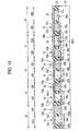
- FIG. 14 is a sectional view of the solid-state image sensor according to the first embodiment of the present invention, in the steps of the method for fabricating the solid-state image sensor, which illustrates the method (Part 12).
- FIG. 15 is a sectional view of the solid-state image sensor according to the first embodiment of the present invention, in the steps of the method for fabricating the solid-state image sensor, which illustrates the method (Part 13).
- FIG. 16 is a sectional view of the solid-state image sensor according to the first embodiment of the present invention, in the steps of the method for fabricating the solid-state image sensor, which illustrates the method (Part 14).
- FIG. 17 is a sectional view of the solid-state image sensor according to the first embodiment of the present invention, in the steps of the method for fabricating the solid-state image sensor, which illustrates the method (Part 15).
- FIG. 18 is a sectional view of the solid-state image sensor according to the first embodiment of the present invention, in the steps of the method for fabricating the solid-state image sensor, which illustrates the method (Part 16).
- FIG. 19 is a sectional view of the solid-state image sensor according to the first embodiment of the present invention, in the steps of the method for fabricating the solid-state image sensor, which illustrates the method (Part 17).
- FIG. 20 is a sectional view of the solid-state image sensor according to the first embodiment of the present invention, in the steps of the method for fabricating the solid-state image sensor, which illustrates the method (Part 18).
- FIG. 21 is a sectional view of the solid-state image sensor according to a modification of the first embodiment of the present invention.
- FIG. 22 is a sectional view of the solid-state image sensor according to a second embodiment of the present invention.
- FIG. 23 is a sectional view of the solid-state image sensor according to the second embodiment of the present invention, in the steps of the method for fabricating the solid-state image sensor, which illustrates the method (Part 1).
- FIG. 24 is a sectional view of the solid-state image sensor according to the second embodiment of the present invention, in the steps of the method for fabricating the solid-state image sensor, which illustrates the method (Part 2).
- FIG. 25 is a sectional view of the solid-state image sensor according to the second embodiment of the present invention, in the steps of the method for fabricating the solid-state image sensor, which illustrates the method (Part 3).
- FIG. 26 is a sectional view of the solid-state image sensor according to the second embodiment of the present invention, in the steps of the method for fabricating the solid-state image sensor, which illustrates the method (Part 4).
- FIG. 27 is a sectional view of the solid-state image sensor according to a modification of the second embodiment of the present invention.
- FIG. 28 is a sectional view of the solid-state image sensor according to a third embodiment of the present invention.
- FIG. 29 is a sectional view of the solid-state image sensor according to the third embodiment of the present invention, in the steps of the method for fabricating the solid-state image sensor, which illustrates the method (Part 1).
- FIG. 30 is a sectional view of the solid-state image sensor according to the third embodiment of the present invention, in the steps of the method for fabricating the solid-state image sensor, which illustrates the method (Part 2).
- FIG. 31 is a sectional view of the solid-state image sensor according to the third embodiment of the present invention, in the steps of the method for fabricating the solid-state image sensor, which illustrates the method (Part 3).
- FIG. 32 is a sectional view of the solid-state image sensor according to the third embodiment of the present invention, in the steps of the method for fabricating the solid-state image sensor, which illustrates the method (Part 4).
- FIG. 33 is a sectional view of the solid-state image sensor according to the third embodiment of the present invention, in the steps of the method for fabricating the solid-state image sensor, which illustrates the method (Part 5).
- FIG. 34 is a sectional view of the solid-state image sensor according to the third embodiment of the present invention, in the steps of the method for fabricating the solid-state image sensor, which illustrates the method (Part 6).
- FIG. 35 is a sectional view of the solid-state image sensor according to the third embodiment of the present invention, in the steps of the method for fabricating the solid-state image sensor, which illustrates the method (Part 7).
- FIG. 36 is a sectional view of the solid-state image sensor according to the third embodiment of the present invention, in the steps of the method for fabricating the solid-state image sensor, which illustrates the method (Part 8).
- FIG. 37 is a sectional view of the solid-state image sensor according to a modification of the third embodiment of the present invention.
- The solid-state image sensor according to a first embodiment of the present invention will be explained with reference to FIGs. 1 to 20 . FIG. 1 is a plan view of the solid-state image sensor according to the present embodiment. FIG. 2 is sectional views of the solid-state image sensor according to the present embodiment.
- First, the solid-state image sensor according to the present embodiment will be explained with reference to FIGS. 1 and 2.
- As illustrated in FIG. 1, the solid-state image sensor according to the present embodiment mainly comprises a
pixel array part 10, a blackpixel array part 12, ananalog circuit part 14, adigital circuit part 16 and an I/O circuit part (input/output circuit part) 18. - The
pixel array part 10 is a region for taking images, and a plurality of pixels are formed in a matrix there. - The black
pixel array part 12 is for taking signals which are to a reference of black color. In the blackpixel array part 12, pixels shielded from light with a shield film 58 (see FIG. 2) is formed. - In the present embodiment, the pixels of the black
pixel array part 12 are shielded from light with theshield film 58. However, the pixels of the black pixel array part may be shielded from light with an interconnection layer formed solidly. - The
analog circuit 14 is for processing analog signals, etc. outputted from the pixel part. Theanalog circuit part 14 comprises, e.g., an amplification circuit for amplifies detected light signals, a signal read/ noise cancellation circuit for reading signals or canceling noises, an A/D converter for converting analog signals to digital signals, etc. In the signal read/noise cancellation circuit, noises are cancelled by, e.g., CDS (Correlated Double Sampling). - The
digital circuit part 16 is for digitizing signals, etc. outputted from theanalog circuit part 14 and other processing. In thedigital circuit part 16, a processor unit for making prescribed signal processing, a timing generator for deciding a timing of reading signals, an SRAM circuit for memorizing data, etc. are formed. - The I/
O circuit part 18 is for inputting/outputting signals to/from the outside. - In FIG. 2, on the right side of the drawing, the
pixel array part 10 is illustrated. On the left side of thepixel array part 10, the blackpixel array part 12 is illustrated. On the left side of the blackpixel array part 12, theanalog circuit part 14 is illustrated. On the left side of theanalog circuit 14, thedigital circuit 16 is illustrated. On the left side of thedigital circuit 16, the I/O circuit part 18 is illustrated. - The
region 10D of thepixel array part 10 on the right side of the drawing is a region where a photodiode (photoelectric conversion device) PD1 is formed, and theregion 10N of thepixel array part 10 on the left side of the drawing is a region where an NMOS transistor is formed. - The
region 12D of the blackpixel array part 12 on the right side of the drawing is a region where a photodiode PD2 is formed, and theregion 12N of the blackpixel array part 12 on the left side of the drawing is a region where an NOMS transistor is formed. - The
region 14P of theanalog circuit part 14 on the right side of the drawing is a region where a PMOS transistor is formed, and theregion 14N of theanalog circuit part 14 on the left side of the drawing is a region where an NMOS transistor is formed. - The
region 16P of thedigital circuit part 16 on the right side of the drawing is a region where a PMOS transistor is formed, and theregion 16N of thedigital circuit part 16 on the left side of the drawing is a region where an NMOS transistor is formed. - The
region 18P of the I/O circuit part 18 on the right side of the drawing is a region where a PMOS transistor is formed, and theregion 18N of the I/O circuit part 18 on the left side of the drawing is a region where an NMOS transistor is formed. -
Device isolation regions 22 for defining the device regions are formed on the surface of a Ptype semiconductor substrate 20. - In the
region 10D of thepixel array part 10, where the photodiode is formed, an N type impurity diffusedregion 24a is formed in thesemiconductor substrate 20. The N type impurity diffusedregion 24a forms the photodiode PD1. On the surface of the device region where the N type impurity diffusedregion 24a is formed, a P type impurity diffusedlayer 26 is formed.Silicon oxide films layer 26. - In the
region 10N of thepixel array part 10, where the NMOS transistor is formed, aP type well 28a is formed. Agate electrode 32 is formed on theP type well 28a with thegate insulation film 30a formed therebetween. The N type lightly doped diffused layer is formed in thesemiconductor substrate 20 on both sides of thegate electrode 32. Asidewall insulation film 34 is formed on the side wall of thegate electrode 32. The N type heavily doped diffused layer is formed in thesemiconductor substrate 20 on both side of thegate electrode 32 with thesidewall insulation film 34 formed on. The N type lightly doped diffused layer and the N type heavily doped diffused layer form a source/drain diffusedlayer 36n of the LDD structure. Thus, theNMOS transistor 38a including thegate electrode 32 and the source/drain diffusedlayer 36n is formed. TheNMOS transistor 38a forms a part of the read circuit of, e.g., thepixel array part 10. - In the
semiconductor substrate 20 of the blackpixel array part 12, an N type buried diffusedlayer 40a is formed. AnN type well 42a is formed, surrounding the region between the surface of thesemiconductor substrate 20 and the N type buried diffusedlayer 40a. TheN type well 42a and the N type buried diffusedlayer 40a are connected to each other at the sides of the N type buried diffusedlayer 40a.A P type well 28b is formed in the region surrounded by the buried diffusedlayer 40a and theN type well 42a. TheP type well 28b is formed in theregion 12N, where the NMOS transistor is formed and also in theregion 12D, where the photodiode is formed. TheP type well 28b is isolated from thepixel array part 10 by the N type buried diffusedlayer 40a and theN type well 42a. This structure is called a triple well structure. - In the
region 12D of the blackpixel array part 12, where the photodiode is formed, an N type impurity diffusedregion 24b is formed in theP type well 28b. The P type impurity diffusedlayer 26 is formed on the surface of the device region where an N type impurity diffusedregion 24b is formed. Thesilicon oxide films layer 26. - In the
region 12N of the blackpixel array part 12, where the NMOS transistor is formed, agate electrode 32 is formed on theP type well 28b with thegate insulation film 30 a formed therebetween. In thesemiconductor substrate 20 on both side of thegate electrode 32, the N type lightly doped diffused layer is formed. Thesidewall insulation film 34 is formed on the side wall of thegate electrode 32. The N type heavily doped diffused layer is formed in thesemiconductor substrate 20 on both sides of thegate electrode 32 with thesidewall insulation film 34 formed on. The N type lightly doped diffused layer and the N type heavily doped diffused layer form the source/drain diffusedlayer 36n of the LDD structure. Thus, theNMOS transistor 38b including the gate electrode and the source/drain diffusedlayer 36n is formed. TheNMOS transistor 38b forms a part of the read circuit of, e.g., the blackpixel array part 12. - In the
region 14N of theanalog circuit region 14, where the NMOS transistor is formed, the N type buried diffusedlayer 40b is buried in thesemiconductor substrate 20. AnN type well 42b is formed, surrounding the region between the surface of thesemiconductor substrate 20 and the buried diffusedlayer 40b. TheN type well 42b is formed in thedevice region 14N, where the NMOS transistor is formed and also in theregion 14P, where the PMOS transistor is formed. TheN type well 42b and the buried diffusedlayer 40b are connected to each other at the sides of the buried diffusedlayer 40b.A P type well 44a is formed in the region surrounded by the buried diffusedlayer 40b and theN type well 42b. TheP type well 44a is electrically isolated from thepixel array part 10 by the buried diffusedlayer 40b and theN type well 42b. - A
gate electrode 32 is formed on theP type well 44a with thegate insulation film 30b. The N type lightly doped diffused layer is formed in thesemiconductor substrate 20 on both sides of thegate electrode 32. Thesidewall insulation film 34 is formed on the side wall of thegate electrode 32. The N type heavily doped diffused layer is formed in thesemiconductor substrate 20 on both sides of thegate electrode 32 with thesidewall insulation film 34 formed on. The N type lightly doped diffused layer and the N type heavily doped diffused layer form the source/drain diffusedlayer 36n of the LDD structure. Thus, theNMOS transistor 38c including thegate electrode 32 and the source/drain diffusedlayer 36n is formed. - On the
N type well 42b in theregion 14P, where the PMOS transistor is formed, agate electrode 32 is formed with thegate insulation film 30b formed therebetween. The P type lightly doped diffused layer is formed in thesemiconductor substrate 20 on both sides of thegate electrode 32. Thesidewall insulation film 34 is formed on the side wall of thegate electrode 32. The P type heavily doped diffused layer is formed in thesemiconductor substrate 20 on both sides of thegate electrode 32 with thesidewall insulation film 34 formed on. The P type lightly doped diffused layer and the P type heavily doped diffused layer form the source/drain diffusedlayer 36p of the LDD structure. Thus, thePMOS transistor 38d including thegate electrode 32 and the source/drain diffusedlayer 36p is formed. TheNMOS transistor 38c and thePMOS transistor 38d form the CMOS circuit. - In the
region 16N of thedigital circuit part 16, where the NMOS transistor is formed, the N type buried diffusedlayer 40c is buried in thesemiconductor substrate 20. AnN type well 42c is formed, surrounding the region between the surface of thesemiconductor substrate 20 and the buried diffusedlayer 40c. TheN type well 42c is formed in thedevice region 16N, where the NMOS transistor is formed and also in theregion 16P, where the PMOS transistor is formed. The buried diffusedlayer 40c and theN type well 42c are connected to each other at the side of the buried diffusedlayer 40c.A P type well 44b is formed in the region surrounded by the buried diffusedlayer 40c and theN type well 42c. TheP type well 44b is electrically isolated from thepixel array part 10 by the buried diffusedlayer 40c and theN type well 42c. - A
gate electrode 32 is formed on theP type well 44b with thegate insulation film 30b formed therebetween. The N type lightly doped diffused layer is formed in thesemiconductor substrate 20 on both sides of thegate electrode 32. Thesidewall insulation film 34 is formed on the side wall of thegate electrode 32. The N type heavily doped diffused layer is formed in thesemiconductor substrate 20 on both sides of theelectrode 32 with thesidewall insulation film 34 formed on. The N type lightly doped diffused layer and the N type heavily doped diffused layer form the source/drain diffusedlayer 36n of the LDD structure. Thus, the NMOS transistor including thegate electrode 32 and the source/drain diffusedlayer 36n is formed. - In the
region 16P of thedigital circuit part 16, where the PMOS transistor is formed, agate electrode 32 is formed on theN type well 42c with thegate insulation film 30b formed therebetween. The P type lightly doped diffused layer is formed in thesemiconductor substrate 20 on both sides of thegate electrode 32. Thesidewall insulation film 34 is formed on the side wall of thegate electrode 32. The P type heavily doped diffused layer is formed in thesemiconductor substrate 20 on both sides of thegate electrode 32 with thesidewall insulation film 34 formed on. The P type lightly doped diffused layer and the P type heavily doped diffused layer form the source/drain diffusedlayer 36p of the LDD structure. Thus, thePMOS transistor 38f including thegate electrode 32 and the source/drain diffusedlayer 36p is formed. TheNMOS transistor 38c and thePMOS transistor 38f form the CMOS circuit. - In the
region 18N of the I/O circuit part 18, where the NMOS transistor is formed, the N type buried diffusedlayer 40d is buried in thesemiconductor substrate 20. AnN type well 42d is formed, surround the region between the surface of thesemiconductor substrate 20 and the buried diffusedlayer 40d. TheN type well 42d is formed in theregion 18N, where the NMOS transistor is formed and also in theregion 18P, where the PMOS transistor is formed. TheN type well 42d and the N type buried diffusedlayer 40d are connected to each other on the side of the buried diffusedlayer 40d.A P type well 44c is formed in the region surrounded by the N type buriedlayer 40d and theN type well 42d. TheP type well 44c is electrically isolated from thepixel array part 10 by the buried diffusedlayer 40d and theN type well 42d. - A
gate electrode 32 is formed on theP type well 44c with thegate insulation film 30a formed therebetween. The N type lightly diffused layer is formed in thesemiconductor substrate 20 on both sides of thegate electrode 32. Thesidewall insulation film 34 is formed on the side wall of thegate electrode 32. The N type heavily doped diffused layer is formed in thesemiconductor substrate 20 on both sides of thegate electrode 32 with thesidewall insulation film 34 formed on. The N type lightly doped diffused layer and the N type heavily doped diffused layer form the source/drain diffusedlayer 36n of the LDD structure. Thus, theNMOS transistor 38g including thegate electrode 32 and he source/drain diffusedlayer 36n is formed. - In the
region 18P of the I/O circuit 18, where the PMOS transistor is formed, agate electrode 32 is formed on theN type well 42d with thegate insulation film 30a formed therebetween. Thesidewall insulation film 34 is formed on the side wall of thegate electrode 32, The P type source/drain diffusedlayer 36p is formed in thesemiconductor substrate 20 onboth sides of thegate electrode 32 with thesidewall insulation film 34 formed on. Thus, thePMOS transistor 38h including thegate electrode 32 and the source/drain diffusedlayer 36p is formed. TheNMOS transistor 38g and thePMOS transistor 38h form the CMOS circuit. - On the source/drain diffused
layer drain electrodes 46a of metal silicide are formed. Also on the upper surfaces of thegate electrodes 32, ametal silicide film 46b is formed. - An
inter-layer insulation film 48 is formed on thesemiconductor substrate 20 with the photodiodes PD1, PD2, theNMOS transistors 38a - 38c, 38e, 38g, thePMOS transistors - In the
inter-layer insulation film 48,contact holes 50a and contactholes 50b are formed respectively down to the source/drain electrodes 46a and down to thegate electrodes 32. - Conductor plugs 52 are buried in the
contact holes - On the
inter-layer insulation film 48 with the conductor plugs 52 buried in,interconnections 54 are formed, connected to the conductor plugs 52. - On the
inter-layer insulation film 48 with theinterconnections 54 formed on, other interconnection layers and other inter-layer insulation layers 56 are formed respectively in plural layers. - A
shield film 58 is formed on theinter-layer insulation film 56. In theshield film 58, anopening 60 is formed in for opening theregion 10D of thepixel array part 10, where the photodiode is formed. The photodiode PD2 of the blackpixel array part 12 is shielded from light by theshield film 58. - As described above, in the present embodiment, the so-called triple well structure is used in the black
pixel array part 12, theanalog circuit part 14, thedigital circuit part 16 and the I/O circuit 18. That is, in the present embodiment, theP type well 28b of theblack pixel arraypart 12 is electrically isolated from thepixel array part 10 by theN type well 42a and the N type buried diffusedlayer 40a, the P type well 44a of theanalog circuit 14 is electrically isolated from thepixel array part 10 by theN type well 42b and the N type buried diffusedlayer 40b, theP type well 44b of thedigital circuit 16 is electrically isolated from thepixel array part 10 by theN type well 42c and the N type buried diffusedlayer 40c, and theP type well 44c of the I/O circuit part 18 is electrically isolated from thepixel array part 10 by theN type well 42d and theN type well 40d. - The
P type well 28b of the blackpixel array part 12 is electrically isolated from thepixel array part 10 by theN type well 42a and the N type buried diffusedlayer 40a, so that when relatively intense light is incident on thepixel array part 10, the inflow of charges into theblack pixel array 12 is prevented to thereby obtain stable reference signals. - The P type well 44a of the
analog circuit part 14 is electrically isolated from thepixel array part 10 by theN type well 42b and the N type buried diffusedlayer 40b, so that the intrusion of noises into theanalog circuit part 14 is prevented, and also the noises generated in theanalog circuit part 14 are prevented from affecting the other components. - The
P type well 44b of thedigital circuit part 16 is electrically isolated from thepixel array part 10 by theN type well 42c and the N type buried diffusedlayer 40c, so that the intrusion of noises into thedigital circuit part 16 is prevented, and also the noises generated in thedigital circuit part 16 are prevented from affecting the other components. - The
P type well 44c of the I/O circuit 18 is electrically isolated from thepixel array part 10 by theN type well 42d and the N type buried diffusedlayer 40d, so that the intrusion of noises into the I/O circuit part 18 is prevented, and also the noises intruding into the I/O circuit part 18 from the outside and the noises generated in the I/O circuit part 18 are prevented from affecting the other components. - The so-called triple structure is not used in the
pixel array part 10 for the following reason. - That is, for the highly efficient photoelectric conversion in the photodiode PD1, it is important that when light is incident on the photodiode PD1 from, the outside, the depletion layer is extended to sufficiently deep region of the
semiconductor substrate 20 . If the N type impurity diffusedregion 24a forming the photodiode PD1 is formed in the P type well, because of the higher impurity concentration of the P type well than that of thesemiconductor substrate 20, the depletion layer cannot easily extend when light is incident on the photodiode PD1. Even if the impurity concentration of the P type well is set lower so as to make it easy for the depletion layer to extend, depletion layer is hindered from extending by the N type buried diffused layer formed below the P type well. Accordingly, the use of the triple well structure in thepixel array part 10 makes it very difficult to realize high quality image. - For this reason, the triple structure is not used in the
pixel array part 10 but used in the blackpixel array part 12, theanalog circuit part 14, thedigital circuit part 16 and the I/O circuit 18, whereby thepixel array part 10 is kept from being affected by the noises. - The solid-state image sensor according to the present embodiment is characterized mainly in that the triple well structure is not used in the
pixel array part 10 but is used in the blackpixel array part 12, theanalog circuit part 14, thedigital circuit part 16 and the I/O circuit part 18. - In the present embodiment, the triple structure is used in the
black pixel part 12, theanalog circuit part 14, thedigital circuit part 16 and the I/O circuit part 18, whereby thepixel array part 10 is kept form being affected by noises. Furthermore, thepixel array part 10, which does not use the triple well structure, can perform highly efficient photoelectric conversion. Accordingly, the solid-state image sensor according to the present embodiment can realize high quality image quality. -
Patent Reference 1 discloses a technique of stabilize the black level by preventing the inflow of charges into the black pixel array part when intense light is incident on the pixels of the pixel array parts. However, it is difficult to realize the drastic improvement of the image quality only by stabilizing the black level.Patent Reference 1 neither discloses nor suggests the technique of the present invention that the triple well structure is used in the analog circuit part, the digital circuit part and the input/output circuit part to thereby realize the drastic improvement of the image quality. - Next, the method for fabricating the solid-state image sensor according to the present embodiment will be explained with reference to FIGs. 3 to 20. FIGs. 3 to 20 are sectional views of the solid-state image sensor according to the present embodiment in the steps of the method for fabricating the solid-state image sensor, which illustrate the method.
- First, as illustrated in FIG. 3, the P
type semiconductor substrate 20 is prepared. Thesemiconductor substrate 20 is, e.g., an epitaxial substrate with, e.g., a 11 µm-thickness silicon layer epitaxially grown on a silicon substrate. The resistivity of thesemiconductor substrate 10 is, e.g., 10 Ω·cm. - Next,
trenches 62 of an about 250 nm-depth are formed in thesemiconductor substrate 20. Then, a silicon oxide film is formed on the entire surface. Then, the silicon oxide film is polished by, e.g., CMP until the surface of thesemiconductor substrate 20 is exposed. The silicon oxide film is thus buried in thetrenches 62 to form thedevice isolation regions 22. Thus, thedevice isolation regions 22 are formed by STI (Shallow Trench Isolation) . - Next, as illustrated in FIG. 4, a
photoresist film 64 is formed on the entire surface by spin coating. - Then, the
photoresist film 64 is patterned by photolithography. Thus, in thephotoresist film 64, anopening 66a is formed to expose the blackpixel array part 12, anopening 66b is formed to expose theregion 14N of theanalog circuit part 14, where the NMOS transistor is to be formed, anopening 66c is formed to expose theregion 16N of thedigital circuit part 16, where the NMOS transistor is to be formed, and anopening 66d is formed to expose theregion 18N of the I/O circuit part 18, where the NMOS transistor is to be formed. - Next, with the
photoresist film 64 as the mask, an N type dopant impurity is implanted by ion implantation. The N type dopant impurity is, e.g., phosphorus (P+) . Conditions for the ion implantations are, e.g., a 1 MeV acceleration energy and a 1×10¹³ - 5×1013 cm-2. Thus, the N type buried diffusedlayer 40a - 40d is buried. The buried diffusedlayer 40a - 40d is buried in the region which is about 1 - 1.5 µm deep from the surface of thesemiconductor substrate 20. Then, thephotoresist film 64 is released. - Next, as illustrated in FIG. 5, a
photoresist film 68 is formed on the entire surface by spin coating. - Next, the
photoresist film 68 is patterned by photolithography. Thus, an opening70a for exposing theregion 14N of theanalog circuit part 14, where the NMOS transistor is to be formed, anopening 70b for exposing theregion 16N of thedigital circuit part 16, where the NMOS transistor is to be formed, and anopening 70c for exposing theregion 18N of the I/O circuit part 18, where the NMOS transistor is to be formed are formed in thephotoresist film 68. - Then, with the
photoresist film 68 as the mask, a P type dopant impurity is introduced by ion implantation. The P type dopant impurity is, e.g., boron (B+) . Conditions for the ion implantation are, e.g., a 300 - 500 keV and a 1×10¹³ - 5×1013 cm-2. Thus, theP type wells 44a - 44c are formed. - A threshold voltage control layer (not illustrated) for controlling threshold voltages of the
NMOS transistors semiconductor substrate 20 with thephotoresist film 58 as a mask, before thephotoresist film 68 is released. In forming the threshold voltage control layer, a P type dopant impurity is introduced in a relative shallow region of thesemiconductor substrate 20 by ion implantation with thephotoresist film 68 as the mask. The P type dopant impurity is, e.g., boron. Conditions for the ion implantation are, e.g., an acceleration energy of 50 keV or below, and a 1×10¹² - 7×1012 cm-2 dose. Then, thephotoresist film 68 is released. - Then, as illustrated in FIG. 6, a
photoresist film 72 is formed on the entire surface by spin coating. - Next, the
photoresist film 72 is patterned by photolithography. Thus, in thephotoresist film 72,openings 74a - 74d for exposing the peripheral edges of the region where the buried diffusedlayers 40a - 40d are formed. Theopening 74b for exposing the peripheral edge of the region where the buried diffusedlayer 40b is formed is formed, exposing also the peripheral edge of theregion 14P of theanalog circuit part 14, where the PMOS transistor is to be formed. Theopening 74c for exposing the peripheral edge of the region where the buried diffusedlayer 40c is formed is formed, exposing also theregion 16P of thedigital circuit part 16, where the PMOS transistor is to be formed. Theopening 74d for exposing the peripheral edge of the region where the buried diffusedlayer 40d is formed is formed, exposing also theregion 18P of the I/O circuit 18, where the PMOS transistor is to be formed. - Next, an N type dopant impurity is introduced by ion implantation with the
photoresist film 72 as the mask. The N type dopant impurity is, e.g., phosphorus (P+) . Conditions for the ion implantation are, e.g., a 500 - 700 keV acceleration energy and a 1×10¹³ - 5×1013 cm-2. Thus, theN type wells 42a - 42d are formed in the blackpixel array part 12, theanalog circuit part 14, thedigital circuit part 16 and the I/O circuit 18. TheN type wells 42a - 42d and the N type buried diffusedlayers 40a - 40d are connected each other at the sides of the N type buried diffusedlayer 40a - 40d. - A threshold voltage control layer (not illustrated) for controlling threshold voltages of the
PMOS transistors semiconductor substrate 20 with thephotoresist film 72 as a mask, before thephotoresist film 72 is released. In forming the threshold voltage control layer, an N type dopant impurity is introduced in a relative shallow region of thesemiconductor substrate 20 by ion implantation with thephotoresist film 72 as the mask. The N type dopant impurity is, e.g., arsenic (As+). Conditions for the ion implantation are, e.g., an acceleration energy of 200 keV or below, and a 1×10¹² - 5×1012 cm-2 dose. Then, thephotoresist film 72 is released. - Then, as illustrated in FIG. 7, a
photoresist film 76 is formed on the entire surface by spin coating. - Then, the
photoresist film 76 is patterned by photolithography. Anopening 78a for exposing theregion 10N of thepixel array part 10, where the NMOS transistor is to be formed, and anopening 78b for exposing the blackpixel array part 14 is formed. - Next, a P type dopant impurity is introduced by ion implantation with the
photoresist film 76 as the mask, The P type dopant impurity is, e.g., boron. Conditions for the ion implantation are, e.g., a 300 - 500 keV acceleration energy and a 1×10¹³ - 5×1013 cm-2. Thus, theP type well 28a is formed in theregion 10N of thepixel arraypart 10, where the NMOS transistor is to be formed. TheP type well 28b is formed in the region of the blackpixel array part 12, which is surrounded by theN type well 42a and the buried diffusedlayer 28b. - A threshold voltage control layer (not illustrated) for controlling threshold voltages of the
NMOS transistors semiconductor substrate 20 with thephotoresist film 76 as a mask, before thephotoresist film 76 is released. In forming the threshold voltage control layer, a P type dopant impurity is introduced in a relative shallow region of thesemiconductor substrate 20 by ion implantation with thephotoresist film 76 as the mask. The P type dopant impurity is, e.g., boron. Conditions for the ion implantation are, e.g., a 50 keV acceleration energy and a 2×10¹² - 7×1012 cm-2 dose. Then, thephotoresist film 76 is released. - Then, as illustrated in FIG. 8, a
photoresist film 80 is formed on the entire surface by spin coating. - Next, the
photoresist film 80 is patterned by photolithography to form in thephotoresist film 80 anopening 82a for exposing the region of thepixel array part 10, where the photodiode PD1 is to be formed, and anopening 82b of the blackpixel array part 12, where the photodiode PD2 is to be formed. - Next, an N type dopant impurity is introduced by ion implantation with the
photoresist film 80 as the mask. The dopant impurity is, e.g., phosphorus. Conditions for the ion implantation are, e.g., a 300 - 500 keV acceleration energy and a 1×10¹² - 5×1012 cm-2. Thus, the N type impurity diffusedregions - The ion implantation may be repeated by plural times to form the N type impurity diffused
region regions photoresist film 80 is released. - Next, as illustrated in FIG. 9, the
gate insulation film 30 of, e.g., a 5 - 8 nm-thickness is formed on the entire surface. - Next, as illustrated in FIG. 10, a
photoresist film 84 is formed on the entire surface by spin coating. - Then, an
opening 86 for exposing theregion 14, where the analog circuit part is to be formed and theregion 16, where the digital circuit part is to be formed is formed in thephotoresist film 84 by photolithography. - Next, with the
photoresist film 84 as the mask, thegate insulation film 30 exposed in theopening 86 is etched off. The etchant is, e.g., hydrofluoric acid. Then, thephotoresist film 84 is released. - Next, by thermal oxidation, the
gate insulation film 30b is formed on the exposed surface of thesemiconductor substrate 20 while adding to the thickness of thegate insulation film 30. The conditions for the thermal oxidation are set so that the thermal oxide film is formed in a 3 nm-thickness on the exposed surface of thesemiconductor substrate 20. Thegate insulation film 30 b is formed in, e. g. , a 3nm-thickness in theanalog circuit part 14 and thedigital circuit part 16. In thepixel array part 10, the blackpixel array part 12 and the I/O circuit part 18, where thegate insulation film 30 has been formed, the film thickness of thegate insulation film 30a there is, e.g., about 8 - 10 nm (see FIG. 11) - Next, as illustrated in FIG. 12, a
polysilicon film 32 of, e.g., a 150 - 200 nm-thickness is formed on the entire surface. - Next, as illustrated in FIG. 13, the
polysilicon film 32 is patterned by photolithography. Thus, thegate electrodes 32 of the polysilicon are formed. - Next, a photoresist film (not illustrated) is formed on the entire surface by spin coating.
- Then, openings (not illustrated) for exposing the
regions - Then, with the photoresist film and the
gate electrodes 32 as the mask, an N type dopant impurity is introduced into thesemiconductor substrate 20 by ion implantation. The dopant impurity is, e.g., arsenic (As+). Conditions for the ion implantation are, e.g., an acceleration energy of 15 keV or below, and a 2×10¹⁴ - 7×1014 cm-2 dose. Thus, the N type lightly doped diffusedlayer 35n is formed in thesemiconductor substrate 20 on both sides of thegate electrodes 32. Then, the photoresist film is released. - Next, a photoresist film (not illustrated) is formed on the entire surface by spin coating.
- Next, openings (not shown) for exposing the
regions - Next, a P type dopant impurity is introduced into the
semiconductor substrate 20 by the ion implantation with the photoresist film and thegate electrodes 32 as the mask. The dopant impurity is, e.g., BF2 +. Conditions for the ion implantation are, e.g., an acceleration energy of 15 keV or below, and a 2×10¹⁴ - 7×1014 cm-2 dose. Thus, the P type lightly doped diffusedlayer 35p is formed in thesemiconductor substrate 20 on both sides of thegate electrodes 32. Then, the photoresist film is released. - Then, a photoresist film (not illustrated) is formed on the entire surface by spin coating.
- Next, openings (not illustrated) for exposing the
regions - Then, a P type dopant impurity is introduced into the
semiconductor substrate 20 by ion implantation with the photoresist film as the mask. The dopant impurity is, e.g., boron (B+). Conditions for the ion implantation are, e.g., a 15 keV acceleration energy and a 1×10¹³ - 5×1013 cm-2 dose. Thus, the P type impurity diffusedlayer 26 is formed on the surface of thesemiconductor substrate 20 in theregions - Next, as illustrated in FIG. 15, the
silicon oxide film 34 of a 100 nm-thickness is formed on the entire surface by, e.g., CVD. Thesilicon oxide film 34 is to be the sidewall insulation film on the side walls of thegate electrodes 32. Thesilicon oxide film 34 functions also as a protection film for protecting the regions where themetal silicide film - Next, as illustrated in FIG. 16, a
photoresist film 88 is formed on the entire surface by spin coating. - Then, the
photoresist film 88 is patterned by photolithography to cover the regions where themetal silicide film - Next, with the
photoresist film 88 as the mask, thesilicon oxide film 34 is anisotropically etched. Thus, the sidewall insulation film of thesilicon oxide film 34 is formed on the side walls of thegate electrodes 32. Thesilicon oxide film 34 remains in the regions where themetal silicide film photoresist film 88 is released. - Then, a photoresist film (not illustrated) is formed on the entire surface by spin coating.
- Next, a photoresist film for exposing the
regions - Then, an N type dopant impurity is implanted by ion implantation with the photoresist film and the
gate electrodes 32 as the mask. The dopant impurity is, e.g., phosphorus (P+), Conditions for the ion implantation are, e.g., an acceleration energy of 20 keV or below, and a 1×10¹⁵ - 5×1015 cm-2 dose. Then, the N type heavily doped diffused layer is formed in thesemiconductor substrate 20 on both sides of thegate electrodes 32. The N type lightly doped diffusedlayer 35n and the N-heavily doped diffused layer form the source/drain diffusedlayer 36n of the LDD structure. Then, the photoresist film is released. - Next, a photoresist film (not illustrated) is formed on the entire surface by spin coating.
- Next, openings (not illustrated) for exposing the
regions - Then, a P type dopant impurity is introduced by ion implantation with the photoresist film and the
gate electrodes 32 as the mask. The P type dopant impurity is, e.g., boron (B+) . Condition for the ion implantation are, e.g., an acceleration energy of 10 keV or below and a 1×10¹⁵ - 5×1015 cm-2 dose. Thus, the P type heavily dopes diffused layer is formed in thesemiconductor substrate 20 on both sides of thegate electrodes 32. The P type lightly doped diffusedlayer 35p and the P type heavily dopes diffused layer form the source/drain diffusedlayer 36p of the LDD structure in theregion 14P of theanalog circuit part 14, where the PMOS transistor is to be formed and in theregion 16P of thedigital circuit part 16, where the PMOS transistor is to be formed. In theregion 18P of the I/O circuit part 18, where the PMOS transistor is to be formed, the source/drain diffusedlayer 36p of the P type heavily doped diffused layer is formed. Then, the photoresist film is released (see FIG. 17). - Next, a metal film of a 10 nm-thickness cobalt film is formed by, e.g., puttering.
- Next, thermal processing is performed to react the cobalt atoms in the metal film and the silicon atoms in the semiconductor substrate with each other. Thus, the
metal silicide film metal silicide film 46a, which are formed on the surface of the source/drain diffusedlayer metal silicide film 46b is formed also on the surfaces of thegate electrodes 32. - The metal film is cobalt film here but is not limited to cobalt film. The metal film may be, e.g., titanium film, and in this case, the metal silicide film is titanium silicide film.
- Next, the metal film which has not reacted is etched off (see FIG. 18).
- Next, as illustrated in FIG. 19, the
silicon oxide film 48 of a 1500 nm-thickness is formed on the entire surface by, e.g., plasma CVD. - Then, the surface of the
silicon oxide film 48 is polished by, e.g., CMP until the film thickness of the silicon oxide film is reduced to about 1000 nm. Thus, the inter-layer insulation film of thesilicon oxide film 48 of, e.g., a 1000 nm-thickness is formed. - Next, the
contact hole inter-layer insulation film 48 respectively down to the source/drain electrode 46a and down to thegate electrode 46b. - Then, a 300 nm-thickness tungsten film is formed on the entire surface by, e.g., CVD.
- Then, the tungsten film is polished by, e.g., CMP until the surface of the
inter-layer insulation film 48 is exposed. Thus, the conductor plugs 52 of, e.g., tungsten are buried in the contact holes. - Next, a 500 nm-
thickness aluminum film 54 is formed by, e.g., sputtering. - Then, the
aluminum film 54 is patterned by photolithography. Thus, the interconnections (a firstmetal interconnection layer) 54 of aluminum are formed. - Then, the step of forming the
inter-layer insulation film 56, the step of forming contact holes and the step of forming interconnections are sequentially repeated to thereby form a plurality of interconnection layers 56, the interconnection layers, etc. - Then, the
shield film 58 is formed on theinter-layer insulation film 56. - Then, the
shield film 58 is patterned by photolithography. Thus, theopening 60 for exposing the region where the photodiode PD1 is formed is formed in theshield film 58. - Thus, the solid-state image sensor according to the present embodiment is fabricated.
- Then, the solid-state image sensor according to a modification of the present embodiment will be explained with reference to FIG. 21. FIG. 21 is a sectional view of the solid-state image sensor according to the present modification.
- The solid-state image sensor according to the present modification is characterized mainly in that the N type well 42e of the
digital circuit part 16 and the N type well 42e of the I/O circuit part 18 are formed integral with each other, in other words, the N type well 42e of thedigital circuit part 16 and the N type well 42e of the I/O circuit part 18 are formed continuous to each other. - The N type buried diffused
layer 40c and theN type well 42e are connected to each other at the side of the buried diffusedlayer 40c. - The N type buried diffused
layer 40d and theN type well 42e are connected to each other at the side of the buried diffusedlayer 40d. - Thus, the N type well 42e of the
digital circuit part 16 and the N type well 42e of the I/O circuit part 16 may be formed continuous to each other. - The solid-state image sensor according to a second embodiment of the present invention and the method for fabricating the solid-state image sensor will be explained with reference to FIGs. 22 to 26. FIG. 22 is a sectional view of the solid-state image sensor according to the present embodiment. The same members of the present invention as those of the solid-state image sensor according to the first embodiment and the method for fabricating the same illustrated in FIGs. 1 to 21 are represented by the same reference numbers not to repeat or to simplify their explanation.
- First, the solid-state image sensor according to the present embodiment will be explained with reference to FIG. 22.
- The solid-state image sensor according to the present embodiment is characterized mainly in that
device isolation regions 22a are formed by LOCOS (Local oxidation of Silicon) . - As illustrated in FIG. 22, in the present embodiment, the
device isolation regions 22a are formed by LOCOS. The thickness of thedevice isolation regions 22a is, e.g., about 300 nm. Thedevice isolation regions 22 are formed down to the depth of about 150 nm from the surface of asemiconductor substrate 20. - Even with the
device isolation regions 22a formed by LOCOS, the solid-state image sensor can have improved image quality, as does the solid-state image sensor according to the first embodiment. - Next, the method for fabricating the solid-state image sensor according to the present embodiment will be explained with reference to FIGs. 23 to 26. FIGs. 23 to 26 are sectional views of the solid-state image sensor according to the present embodiment in the steps of the method for fabricating the solid-state image sensor, which illustrate the method.
- First, as illustrated in FIG. 23, a 3 - 10 nm-thickness
silicon oxide film 90 is formed on the entire surface by, e. g. , thermal oxidation. - Then, a 100 - 150 nm-thickness
silicon nitride film 92 is formed on the entire surface by, e.g., CVD. - Next, as illustrated in FIG. 24, a
photoresist film 94 is formed on the entire surface by spin coating. - Then,
openings 96 for exposing the regions for thedevice isolation regions 22a to be formed in are formed in thephotoresist film 94 by photolithography. - Next, with the
photoresist film 94 as the mask, thesilicon nitride film 92 and thesilicon oxide film 90 are etched. Then, thephotoresist film 94 is released. - Then, the
semiconductor substrate 20 is oxidized by thermal oxidation selectively at the parts which are not covered by thesilicon nitride film 92. Thus, thedevice isolation regions 22a of the silicon oxide film are formed by LOCOS. - Next, the
silicon nitride film 92 is etched off. The etchant is, e.g., boiled phosphoric acid (see FIG. 25). - The steps of the method for fabricating the solid-state image sensor according to the second embodiment, which will follow hereafter are the same as those of the method for fabricating the solid-state image sensor described above with reference to FIG. 4 to 20, and their explanation will not be repeated.
- Thus, the solid-state image sensor according to the present embodiment is fabricated (see FIG. 26).
- Next, the modification of the solid-state image sensor according to the present embodiment will be explained with reference to FIG. 27. FIG. 27 is a sectional view of the solid-state image sensor according to the present modification.
- The solid-state image sensor according to the present modification is characterized mainly in that the N type well 42e of a
digital circuit part 16 and the N type well 42e of an I/O circuit part 18 are formed integral with each other. In other words, the N type well 42e of thedigital circuit part 16 and the N type well 42e of the I/O circuit 18 are formed continuous to each other. - Thus, the N type well 42e of the
digital circuit part 16 and the N type well 42e of the I/O circuit part 18 may be formed integral with each other. - The solid-state image device according to a third embodiment of the present invention and the method for fabricating the solid-state image sensor will be explained with reference to FIGs. 28 to 36. FIG. 28 is a sectional view of the solid-state image sensor according to the present embodiment. The same members of present embodiments as those of the solid-state image sensor according to the first or the second embodiment and the method for fabricating the semiconductor device illustrated in FIGs. 1 to 27 are represented by the same reference numbers not to repeat or to simplify their explanation.
- First, the solid-state image sensor according to the present embodiment will be explained with reference to FIG. 28.
- The solid-state image sensor according to the present embodiment is characterized mainly in that a P type well is formed in an N type well to thereby form the triple structure.
- As illustrated in FIG. 28, in a
region 10D of apixel array part 10, where a photodiode is formed, an N type impurity diffusedregion 24c is formed in asemiconductor substrate 20. The N type impurity diffusedregion 24c forms a photodiode PD1. - In a
region 10N of thepixel array part 10, where an NMOS transistor is formed, aP type well 100a is formed. AnNMOS transistor 38a is formed o theP type well 100a. - An
N type well 98a is formed in thesemiconductor substrate 20 of a blackpixel array part 12.A P type well 100b is formed in theN type well 98a. TheP type well 100b is formed by implanting a P type dopant impurity into theN type well 98a. TheP type well 100b is formed in aregion 12N where an NMOS transistor is formed and also in aregion 12D where a photodiode PD2 is formed. TheP type well 100b is electrically isolated from thepixel array part 10 by theN type well 98a. - In a
region 12D of the blackpixel array part 12, where a photodiode is formed, an N type impurity diffusedregion 24d is formed in theP type well 100b. - In the
region 12N of the blackpixel array part 12, where an NMOS transistor is formed, anNMOS transistor 38b is formed on theP type well 100b. - In the
semiconductor substrate 20 of ananalog circuit part 14, anN type well 98b is formed. TheN type well 98b is formed in aregion 14N where an NMOS transistor is formed and also in aregion 14P where a PMOS transistor is formed. In theregion 14N of theanalog circuit part 14, where the NMOS transistor is formed, aP type well 100c is formed in theN type well 98b. TheP type well 100c is formed by implanting a P type dopant impurity into theN type well 98b. TheP type well 100c is electrically isolated from thepixel array part 10 by theN type well 98b. AnNMOS transistor 38c is formed on theP type well 100c. In theregion 14P of theanalog circuit part 14, where the PMOS transistor is formed, aPMOS transistor 38d is formed on theN type well 98b. - In the
semiconductor substrate 20 of adigital circuit part 16, anN type well 98c is formed. TheN type well 98c is formed in aregion 16N where an NMOS transistor is formed and also in aregion 16P where a PMOS transistor is formed. In theregion 16N of thedigital circuit part 16, where the NMOS transistor is formed, aP type well 100d is formed in theN type well 98c. TheP type well 100d is formed by implanting a P type dopant impurity into theN type well 98c. TheP type well 100d is electrically isolated from thepixel array part 10 by theN type well 98c. AnNMOS transistor 38e is formed on theP type well 100d. In theregion 16P of thedigital circuit part 16, where the PMOS transistor is formed, aPMOS transistor 38f is formed on theN type well 98c. - In the
semiconductor substrate 20 of an I/O circuit part 18, anN type well 98d is formed. TheN type well 98d is formed in aregion 18N where an NMOS transistor is formed and also in aregion 18P where a PMOS transistor is formed. In theregion 18N of the I/O circuit part 18, where the NMOS transistor is formed, aP type well 100e is formed in theN type well 98d. TheP type well 100e is formed by implanting a P type dopant impurity into theN type well 98d. TheP type well 100e is electrically isolated from thepixel array part 10 by theN type well 98d. AnNMOS transistor 38g is formed on theP type well 100e. In theregion 18P of the I/O circuit part 18, where the PMOS transistor is formed, aPMOS transistor 38h is formed on theN type well 98d. - Thus, the solid-state image sensor according to the present embodiment is formed.
- Thus, the P type well 100b - 100e are formed by implanting P type dopant impurity into the N type well 98a - 98d.
- Then, the method for fabricating the solid-state image sensor according to the present embodiment will be explained with reference to FIGs. 29 to 36. FIGs. 29 to 36 are sectional views of the solid-state image sensor according to the present embodiment in the steps of the method for fabricating the solid-state image sensor, which illustrate the method.
- First, as illustrated in FIG. 29, a 3 - 10 nm-thickness
silicon oxide film 90 is formed on the entire surface by, e.g., thermal oxidation. - Next, a 100 - 150 nm-thickness
silicon nitride film 92 is formed on the entire surface by, e.g., CVD. - Then, as illustrated in FIG 30, a
photoresist film 94 is formed on the entire surface by spin coating. - Then,
openings 96 for exposing the regions wheredevice isolation regions 22a are to be formed are formed in thephotoresist film 94 by photolithography. - Then, with the
photoresist film 94 as the mask, thesilicon nitride film 92 and thesilicon oxide film 90 are etched. Then, thephotoresist film 94 is released. - Next, as illustrated in FIG. 31, a
photoresist film 102 is formed on the entire surface by pin coating. - Then, an
opening 104a for exposing theregion 12, where the black array pixel array part is to be formed, anopening 104b for exposing theregion 14, where the analog circuit part is to be formed, anopening 104c for exposing theregion 16, where the digital circuit part is to be formed, and anopening 104d for exposing theregion 18, where the I/O circuit part is to be formed are formed in thephotoresist film 102 by photolithography. - Then, an N type dopant impurity is introduced into the
semiconductor substrate 20 by ion implantation with thephotoresist film 102 as the mask. Conditions for the ion implantation are, e.g., a 150 - 300 keV acceleration energy and a 1×10¹³ - 5×1013 cm-2 dose. Thus, theN type wells 98a - 98d are formed in the semiconductor substrate. Then, thephotoresist film 102 is released. - Next, thermal processing is performed to diffuse the dopant impurity in the
N type wells 98a - 98d. The atmosphere for the thermal processing is, e.g., nitrogen atmosphere. The thermal processing temperature is, e.g., 1100 °C. The thermal processing period of time is, e.g., 100 minutes. - Then, the
semiconductor substrate 20 is oxidized by thermal oxidation selectively at the parts thereof which are not covered by thesilicon nitride film 92. Thus, thedevice isolation regions 22a of the silicon oxide film are formed. Thus, thedevice isolation regions 22a are formed by LOCOS (see FIG. 32) . By the thermal process in the nitrogen atmosphere and the thermal processing for forming thedevice isolation regions 22a, theN type wells 98a - 98d are formed down to, e.g., an bout 3 µm-depth from the surface of thesemiconductor substrate 20. - Next, the
silicon nitride film 92 is etched off. The etchant is, e.g., boiled phosphoric acid. - The
device isolation regions 22a are formed here after the thermal processing for diffusing the N type dopant impurity implanted in theN type wells 98a - 98d has been performed, but the thermal processing for diffusing the N type dopant impurity may be performed after thedevice isolation regions 22a have been formed. - Then, as illustrated in FIG. 33, a
photoresist film 106 is formed on the entire surface by spin coating. - Next, the
photoresist film 106 is patterned by photolithography. Thus, theopening 108a for exposing theregion 10N of thepixel array part 10, where the NMOS transistor is to be formed, theopenings 108b for exposing the blackpixel array part 12, theopening 108c for exposing theregion 14N of theanalog circuit 14, where the NMOS transistor is to be formed, theopening 108d for exposing theregion 16N of thedigital circuit part 16, where the NMOS transistor is to be formed, and theopening 108e for exposing theregion 18N of the I/O circuit part 18, where the NMOS transistor is to be formed are formed in thephotoresist film 106. - Then, a P type dopant impurity is introduced into the
semiconductor substrate 20 by ion implantation with thephotoresist film 106 as the mask. The P type dopant impurity is, e.g., boron. Conditions for the ion implantation are, e.g., a 100 - 300 keV acceleration energy and a 1×10¹³ - 5×1013 cm-2 dose. - Then, a threshold voltage control layer (not illustrated) for controlling threshold voltages of the
NMOS transistors 38a - 38c, 30e, 38g may be formed by using thephotoresist film 106 before thephotoresist film 106 is released. In forming the threshold voltage control layer, with thephotoresist film 106 as the mask, a P type dopant impurity is introduced by ion implantation into regions of thesemiconductor substrate 20 which are relatively shallow. The P type dopant impurity is, e.g., boron. Conditions for the ion implantation are, e.g., a 50 keV acceleration energy or below, and a 1×10¹² - 7×1012 cm-2 dose. Then, thephotoresist film 106 is released. - Then, in the same way as in the method for fabricating the solid-state image sensor illustrated in FIGs. 9 to 11, a relatively thick
gate insulation film 30a is formed in thepixel array part 10, the blackpixel array part 12 and the I/O circuit part 18, and the relatively thingate insulation film 30b is formed in thedigital circuit part 14 and the analog circuit part 16 (see FIG. 34) - A threshold voltage control layer (not illustrated) for controlling threshold voltages of the transistors 38 may be formed by implanting a dopant impurity into the entire surface of the
semiconductor substrate 20 before or immediately after the step of forming thegate insulation film - Next, in the same way as in the method for fabricating the solid-state image sensor illustrated in FIGs. 12 and 13, the
gate electrodes 32 is formed. - Then, as illustrated in FIG. 35, a
photoresist film 110 is formed on the entire surface by spin coating. - Then, the
photoresist film 110 is patterned by photolithography. Thus, in thephotoresist film 110, anopening 112a for exposing theregion 10D of thepixel array part 10, where the photodiode is to be formed, and anopening 112b for exposing theregion 12D of the blackpixel array part 12, where the photodiode is to be formed. - Next, an N type dopant impurity is introduced by ion implantation with the
photoresist film 110 as the mask. The dopant impurity is, e.g., phosphorus. Conditions for the ion implantation are, e.g., a 20 - 500 keV acceleration energy and a 1×10¹⁴ - 5×1015 cm-2 dose. Thus, the N type impurity diffusedregions photoresist film 110 is released. - The following steps of the method for fabricating the solid-state image sensor are the same as those of the method for fabricating the solid-state image sensor described above with reference to FIGs. 15 to 20, and their explanation will not be repeated.
- Thus, the solid-state image sensor according to the present embodiment is fabricated (see FIG. 36).
- Next, the solid-state image sensor according to the present embodiment will be explained with reference to FIG. 37. FIG. 37 is a sectional view of the solid-state image sensor according to the present modification.
- The solid-state image sensor according to the present modification is characterized mainly in that the N type well 98e of the
digital circuit part 16 and the N type well 98e of the I/O circuit part 18 are formed integral with each other. In other words, the N type well 98e of thedigital circuit part 16 and the N type well 98e of the I/O circuit part 18 are formed continuous to each other. - Thus, the N type well 98e of the
digital circuit part 16 and the N type well 98e of the I/O circuit part 18 may be formed integral with each other. - The present invention is not limited to the above-described embodiments and can cover other various modifications.
- For example, in the above-described embodiments, the
semiconductor substrate 20 is a P type semiconductor substrate. However, thesemiconductor substrate 20 may be an N type semiconductor substrate, and in this case, the conduction types of the respective components are set oppositely.
Claims (14)
- A solid-state image sensor comprising: a pixel part including photoelectric converter for photoelectrically converting incident light, which is formed in a semiconductor substrate of a first conduction type; an analog circuit part for processing an analog signal outputted by the pixel part; a digital circuit part for digital processing a signal outputted by the analog circuit part; and an input/output circuit part for inputting a signal to an outside or outputting a signal from the outside,
the digital circuit part including a first well of a second conduction type different from the first conduction type formed in a second region of the semiconductor substrate surrounding a first region thereof; a first buried diffused layer of the second conduction type buried in the semiconductor substrate in the first region and connected to the first well at the side thereof; a second well of the first conduction type formed near a surface of the semiconductor substrate of the first region; and a first transistor formed on the second well; and
the input/output circuit part including a third well of the second conduction type formed in a fourth region of the semiconductor substrate surrounding a third region; a second buried diffused layer of the second conduction type buried in the semiconductor substrate in the third region and connected to the third well at the side thereof; a fourth well of the first conduction type formed near the surface of the semiconductor substrate in the third region; and a second transistor formed on the fourth well. - A solid-state image sensor according to claim 1, wherein
the analog circuit part includes a fifth well of the second conduction type formed in a sixth region of the semiconductor substrate surrounding a fifth region thereof; a third buried diffused layer of the second conduction type buried in the semiconductor substrate in the fifth region and connected to the fifth well at the side thereof; a sixth well of the first conduction type formed near the surface of the semiconductor substrate in the third region; and a third transistor formed on the sixth well. - A solid-state image sensor according to claim 1, further comprising
another pixel part including a fifth well of the second conduction type formed in a sixth region of the semiconductor substrate surrounding the fifth region thereof; a third buried diffused layer of the second conduction type buried in the semiconductor substrate in the fifth region and connected to the fifth well at the side thereof; a sixth well of the first conduction type formed near the surface of the semiconductor substrate in the fifth region; and another photoelectric converter formed in the sixth well and shielded from light. - A solid-state image sensor comprising: a pixel part including photoelectric converter for photoelectrically converting incident light, which is formed in a semiconductor substrate of a first conduction type; an analog circuit part for processing an analog signal outputted by the pixel part; a digital circuit part for digital processing a signal outputted by the analog circuit part; and an input/output circuit part for inputting a signal to an outside or outputting a signal from the outside,
the digital circuit part including a first well of a second conduction type different from the first conduction type formed in the semiconductor substrate; a second well of the first conduction type formed in the first well; and a first transistor formed on the second well, and
the input/output circuit part including a third well of the second conduction type formed in the semiconductor substrate; a fourth well of the first conduction type formed in the third well; and a second transistor formed on the fourth well. - A solid-state image sensor according to claim 4, wherein
the analog circuit part includes a fifth well of the second conduction type formed in the semiconductor substrate; a sixth well of the first conduction type formed in the fifth well; and a third transistor formed on the sixth well. - A solid-state image sensor according to claim 4, further comprising
a fifth well of the second conduction type formed in the semiconductor substrate; a sixth well of the first conduction type formed in the fifth well; and another photoelectric converter formed in the sixth well and shielded from light. - A solid-state image sensor according to claim 1, wherein
the first well and the third well are formed integral with each other. - A solid-state image sensor according to claim 4, wherein
the first well and the third well are formed integral with each other. - A solid-state image sensor according to claim 1, further comprising:a third transistor formed on the first well; anda fourth transistor formed on the third well.
- A solid-state image sensor according to claim 4, further comprising:a third transistor formed on the first well; anda fourth transistor formed on the third well.
- A solid-state image sensor according to claim 2, further comprising
a fourth transistor formed on the fifth well. - A solid-state image sensor according to claim 5, further comprising
a fourth transistor formed on the fifth well. - A solid-state image sensor according to claim 3, further comprising
a third transistor formed on the sixth well. - A solid-state image sensor according to claim 6, further comprising
a third transistor formed on the sixth well.
Applications Claiming Priority (1)
| Application Number | Priority Date | Filing Date | Title |
|---|---|---|---|
| JP2004210081A JP2006032688A (en) | 2004-07-16 | 2004-07-16 | Solid state imaging apparatus |
Publications (3)
| Publication Number | Publication Date |
|---|---|
| EP1617480A2 true EP1617480A2 (en) | 2006-01-18 |
| EP1617480A3 EP1617480A3 (en) | 2006-11-22 |
| EP1617480B1 EP1617480B1 (en) | 2011-05-11 |
Family
ID=34930903
Family Applications (1)
| Application Number | Title | Priority Date | Filing Date |
|---|---|---|---|
| EP04257686A Expired - Fee Related EP1617480B1 (en) | 2004-07-16 | 2004-12-10 | Solid-state image sensor |
Country Status (6)
| Country | Link |
|---|---|
| US (1) | US7005690B2 (en) |
| EP (1) | EP1617480B1 (en) |
| JP (1) | JP2006032688A (en) |
| KR (1) | KR100671807B1 (en) |
| CN (1) | CN100418230C (en) |
| TW (1) | TWI249850B (en) |
Cited By (5)
| Publication number | Priority date | Publication date | Assignee | Title |
|---|---|---|---|---|
| EP1865557A1 (en) * | 2006-06-06 | 2007-12-12 | Matsushita Electric Industrial Co., Ltd. | MOS solid-state image pickup device and manufacturing method thereof |
| EP2112690A1 (en) * | 2008-04-21 | 2009-10-28 | Sony Corporation | Solid-state imaging device and method of manufacturing the same and electronic apparatus |
| US9136302B2 (en) | 2012-04-27 | 2015-09-15 | Taiwan Semiconductor Manufacturing Company, Ltd. | Apparatus for vertically integrated backside illuminated image sensors |
| US9153565B2 (en) | 2012-06-01 | 2015-10-06 | Taiwan Semiconductor Manufacturing Company, Ltd. | Image sensors with a high fill-factor |
| US10090349B2 (en) | 2012-08-09 | 2018-10-02 | Taiwan Semiconductor Manufacturing Company, Ltd. | CMOS image sensor chips with stacked scheme and methods for forming the same |
Families Citing this family (13)
| Publication number | Priority date | Publication date | Assignee | Title |
|---|---|---|---|---|
| US7919827B2 (en) * | 2005-03-11 | 2011-04-05 | Taiwan Semiconductor Manufacturing Co., Ltd. | Method and structure for reducing noise in CMOS image sensors |
| US7830412B2 (en) * | 2005-08-22 | 2010-11-09 | Aptina Imaging Corporation | Method and apparatus for shielding correction pixels from spurious charges in an imager |
| JP4584159B2 (en) * | 2006-02-24 | 2010-11-17 | セイコーインスツル株式会社 | Semiconductor device and manufacturing method of semiconductor device |
| US20070246788A1 (en) * | 2006-04-21 | 2007-10-25 | Mauritzson Richard A | N-well barrier pixels for improved protection of dark reference columns and rows from blooming and crosstalk |
| JP2007317741A (en) * | 2006-05-23 | 2007-12-06 | Matsushita Electric Ind Co Ltd | Solid-state imaging device and manufacturing method therefor |
| KR20090128902A (en) * | 2008-06-11 | 2009-12-16 | 크로스텍 캐피탈, 엘엘씨 | Method for manufacturing cmos image sensor using dual hardmask |
| KR101435519B1 (en) * | 2008-07-24 | 2014-08-29 | 삼성전자주식회사 | Image sensor having light focusing structure |
| CN101388393B (en) * | 2008-08-26 | 2012-11-14 | 矽创电子股份有限公司 | Polarity switching construction for point converting system |
| US8253200B2 (en) * | 2008-11-19 | 2012-08-28 | Omnivision Technologies, Inc. | Lightly-doped drains (LDD) of image sensor transistors using selective epitaxy |
| JP5810493B2 (en) * | 2010-09-03 | 2015-11-11 | ソニー株式会社 | Semiconductor integrated circuit, electronic equipment, solid-state imaging device, imaging device |
| US9537040B2 (en) * | 2013-05-09 | 2017-01-03 | United Microelectronics Corp. | Complementary metal-oxide-semiconductor image sensor and manufacturing method thereof |
| JP6484513B2 (en) * | 2014-10-08 | 2019-03-13 | 株式会社テクノロジーハブ | Image sensor |
| WO2023189964A1 (en) * | 2022-03-31 | 2023-10-05 | ラピスセミコンダクタ株式会社 | Semiconductor device and method for manufacturing semiconductor device |
Citations (5)
| Publication number | Priority date | Publication date | Assignee | Title |
|---|---|---|---|---|
| JPH05129572A (en) * | 1991-10-31 | 1993-05-25 | Canon Inc | Solid-state image sensor |
| US5537075A (en) * | 1993-12-17 | 1996-07-16 | Sony Corporation | Semiconductor integrated circuit having isolated supply paths for circuit blocks |
| JPH11317667A (en) * | 1998-03-04 | 1999-11-16 | Fujitsu Ltd | Mixture signal circuit and integrated circuit device |
| US6023293A (en) * | 1996-03-12 | 2000-02-08 | Sharp Kabushiki Kaisha | Active type solid-state imaging device |
| US6403998B1 (en) * | 1998-11-09 | 2002-06-11 | Kabushiki Kaisha Toshiba | Solid-state image sensor of a MOS structure |
Family Cites Families (12)
| Publication number | Priority date | Publication date | Assignee | Title |
|---|---|---|---|---|
| US5324982A (en) * | 1985-09-25 | 1994-06-28 | Hitachi, Ltd. | Semiconductor memory device having bipolar transistor and structure to avoid soft error |
| JPS63102371A (en) * | 1986-10-20 | 1988-05-07 | Matsushita Electronics Corp | Manufacture of semiconductor device |
| JP2977056B2 (en) | 1991-10-22 | 1999-11-10 | オリンパス光学工業株式会社 | Solid-state imaging device |
| JP3208307B2 (en) * | 1995-11-27 | 2001-09-10 | 三洋電機株式会社 | Optical semiconductor device |
| US6169318B1 (en) * | 1998-02-23 | 2001-01-02 | Polaroid Corporation | CMOS imager with improved sensitivity |
| JP2000232214A (en) * | 1999-02-12 | 2000-08-22 | Nikon Corp | Semiconductor integrated circuit and solid-state imaging element |
| JP2002199289A (en) | 2000-12-25 | 2002-07-12 | Canon Inc | Photoelectric converter and solid-state image pickup system with it |
| JP4489319B2 (en) * | 2001-04-26 | 2010-06-23 | 富士通マイクロエレクトロニクス株式会社 | Solid-state imaging device |
| JP2002334974A (en) | 2001-05-07 | 2002-11-22 | Nikon Corp | Solid-state imaging device and manufacturing method therefor |
| JP2003274292A (en) * | 2002-03-14 | 2003-09-26 | Sony Corp | Solid-state image pickup device and method of driving the same |
| TWI289905B (en) * | 2002-07-23 | 2007-11-11 | Fujitsu Ltd | Image sensor and image sensor module |
| JP3792628B2 (en) * | 2002-09-02 | 2006-07-05 | 富士通株式会社 | Solid-state imaging device and image reading method |
-
2004
- 2004-07-16 JP JP2004210081A patent/JP2006032688A/en active Pending
- 2004-12-06 US US11/003,380 patent/US7005690B2/en active Active
- 2004-12-07 TW TW093137773A patent/TWI249850B/en not_active IP Right Cessation
- 2004-12-10 EP EP04257686A patent/EP1617480B1/en not_active Expired - Fee Related
- 2004-12-21 KR KR1020040109650A patent/KR100671807B1/en active IP Right Grant
-
2005
- 2005-01-06 CN CNB2005100042556A patent/CN100418230C/en not_active Expired - Fee Related
Patent Citations (5)
| Publication number | Priority date | Publication date | Assignee | Title |
|---|---|---|---|---|
| JPH05129572A (en) * | 1991-10-31 | 1993-05-25 | Canon Inc | Solid-state image sensor |
| US5537075A (en) * | 1993-12-17 | 1996-07-16 | Sony Corporation | Semiconductor integrated circuit having isolated supply paths for circuit blocks |
| US6023293A (en) * | 1996-03-12 | 2000-02-08 | Sharp Kabushiki Kaisha | Active type solid-state imaging device |
| JPH11317667A (en) * | 1998-03-04 | 1999-11-16 | Fujitsu Ltd | Mixture signal circuit and integrated circuit device |
| US6403998B1 (en) * | 1998-11-09 | 2002-06-11 | Kabushiki Kaisha Toshiba | Solid-state image sensor of a MOS structure |
Cited By (9)
| Publication number | Priority date | Publication date | Assignee | Title |
|---|---|---|---|---|
| EP1865557A1 (en) * | 2006-06-06 | 2007-12-12 | Matsushita Electric Industrial Co., Ltd. | MOS solid-state image pickup device and manufacturing method thereof |
| US7755150B2 (en) | 2006-06-06 | 2010-07-13 | Panasonic Corporation | MOS solid-state image pickup device and manufacturing method thereof |
| EP2112690A1 (en) * | 2008-04-21 | 2009-10-28 | Sony Corporation | Solid-state imaging device and method of manufacturing the same and electronic apparatus |
| US8298851B2 (en) | 2008-04-21 | 2012-10-30 | Sony Corporation | Method of manufacturing a solid-state imaging device with a silicide blocking layer and electronic apparatus |
| US8390043B2 (en) | 2008-04-21 | 2013-03-05 | Sony Corporation | Solid-state imaging device with stress-relieving silicide blocking layer and electronic apparatus comprising said solid-state device |
| US9136302B2 (en) | 2012-04-27 | 2015-09-15 | Taiwan Semiconductor Manufacturing Company, Ltd. | Apparatus for vertically integrated backside illuminated image sensors |
| US9153565B2 (en) | 2012-06-01 | 2015-10-06 | Taiwan Semiconductor Manufacturing Company, Ltd. | Image sensors with a high fill-factor |
| US9443836B2 (en) | 2012-06-01 | 2016-09-13 | Taiwan Semiconductor Manufacturing Company, Ltd. | Forming pixel units of image sensors through bonding two chips |
| US10090349B2 (en) | 2012-08-09 | 2018-10-02 | Taiwan Semiconductor Manufacturing Company, Ltd. | CMOS image sensor chips with stacked scheme and methods for forming the same |
Also Published As
| Publication number | Publication date |
|---|---|
| KR100671807B1 (en) | 2007-01-19 |
| TW200605341A (en) | 2006-02-01 |
| EP1617480A3 (en) | 2006-11-22 |
| CN1722455A (en) | 2006-01-18 |
| TWI249850B (en) | 2006-02-21 |
| US7005690B2 (en) | 2006-02-28 |
| KR20060006717A (en) | 2006-01-19 |
| JP2006032688A (en) | 2006-02-02 |
| US20060011956A1 (en) | 2006-01-19 |
| CN100418230C (en) | 2008-09-10 |
| EP1617480B1 (en) | 2011-05-11 |
Similar Documents
| Publication | Publication Date | Title |
|---|---|---|
| EP1617480B1 (en) | Solid-state image sensor | |
| CN101937922B (en) | Method of manufacturing photoelectric conversion device | |
| KR100416821B1 (en) | Solid state imaging device, method of manufacturing the same and solid state imaging system | |
| EP2284896B1 (en) | Solid state imaging device having a photodiode and a MOSFET | |
| US7119387B2 (en) | Solid-state image sensor and method for fabricating the same | |
| US7595210B2 (en) | Method of manufacturing complementary metal oxide semiconductor image sensor | |
| US7700399B2 (en) | Method of making CMOS image sensor—hybrid silicide | |
| US20120119272A1 (en) | Solid-state image sensor, method of manufacturing the same, and imaging system | |
| KR100853792B1 (en) | CMOS Image Sensor and Method of Manufaturing Thereof | |
| KR100562668B1 (en) | A fabricating method of image sensor with decreased dark signal | |
| JP2921567B1 (en) | Solid-state imaging device and method of manufacturing the same | |
| US20090166687A1 (en) | Image Sensor and Method for Manufacturing the Same | |
| JP4763242B2 (en) | Solid-state imaging device and manufacturing method thereof | |
| US20070063303A1 (en) | CMOS image sensor and method for manufacturing the same | |
| US20070051990A1 (en) | CMOS image sensor and method for fabricating the same | |
| JP3621273B2 (en) | Solid-state imaging device and manufacturing method thereof | |
| US7459332B2 (en) | CMOS image sensor and method for manufacturing the same | |
| KR100838466B1 (en) | A fabricating method of image sensor with improved high intergation | |
| CN113629090A (en) | Pixel, image sensor, manufacturing method of pixel and image sensor, and image acquisition device | |
| KR100936103B1 (en) | Image Sensor and Method for Manufacturing the same | |
| JP3881134B2 (en) | MOS sensor and manufacturing method thereof | |
| US7586169B2 (en) | Image sensor and method for manufacturing the same | |
| JP2008177620A (en) | Solid-state imaging device | |
| JP2000196059A (en) | Solid-state image pickup device and its manufacture | |
| KR20070071017A (en) | Image sensor and method for manufacturing the same |
Legal Events
| Date | Code | Title | Description |
|---|---|---|---|
| PUAI | Public reference made under article 153(3) epc to a published international application that has entered the european phase |
Free format text: ORIGINAL CODE: 0009012 |
|
| AK | Designated contracting states |
Kind code of ref document: A2 Designated state(s): AT BE BG CH CY CZ DE DK EE ES FI FR GB GR HU IE IS IT LI LT LU MC NL PL PT RO SE SI SK TR |
|
| AX | Request for extension of the european patent |
Extension state: AL BA HR LV MK YU |
|
| PUAL | Search report despatched |
Free format text: ORIGINAL CODE: 0009013 |
|
| AK | Designated contracting states |
Kind code of ref document: A3 Designated state(s): AT BE BG CH CY CZ DE DK EE ES FI FR GB GR HU IE IS IT LI LT LU MC NL PL PT RO SE SI SK TR |
|
| AX | Request for extension of the european patent |
Extension state: AL BA HR LV MK YU |
|
| 17P | Request for examination filed |
Effective date: 20070305 |
|
| AKX | Designation fees paid |
Designated state(s): DE FR GB IT |
|
| 17Q | First examination report despatched |
Effective date: 20070807 |
|
| RAP1 | Party data changed (applicant data changed or rights of an application transferred) |
Owner name: FUJITSU MICROELECTRONICS LIMITED |
|
| RAP1 | Party data changed (applicant data changed or rights of an application transferred) |
Owner name: FUJITSU SEMICONDUCTOR LIMITED |
|
| GRAP | Despatch of communication of intention to grant a patent |
Free format text: ORIGINAL CODE: EPIDOSNIGR1 |
|
| GRAS | Grant fee paid |
Free format text: ORIGINAL CODE: EPIDOSNIGR3 |
|
| GRAA | (expected) grant |
Free format text: ORIGINAL CODE: 0009210 |
|
| AK | Designated contracting states |
Kind code of ref document: B1 Designated state(s): DE FR GB IT |
|
| REG | Reference to a national code |
Ref country code: GB Ref legal event code: FG4D |
|
| REG | Reference to a national code |
Ref country code: DE Ref legal event code: R096 Ref document number: 602004032624 Country of ref document: DE Effective date: 20110622 |
|
| PLBE | No opposition filed within time limit |
Free format text: ORIGINAL CODE: 0009261 |
|
| STAA | Information on the status of an ep patent application or granted ep patent |
Free format text: STATUS: NO OPPOSITION FILED WITHIN TIME LIMIT |
|
| 26N | No opposition filed |
Effective date: 20120214 |
|
| PG25 | Lapsed in a contracting state [announced via postgrant information from national office to epo] |
Ref country code: IT Free format text: LAPSE BECAUSE OF FAILURE TO SUBMIT A TRANSLATION OF THE DESCRIPTION OR TO PAY THE FEE WITHIN THE PRESCRIBED TIME-LIMIT Effective date: 20110511 |
|
| REG | Reference to a national code |
Ref country code: DE Ref legal event code: R097 Ref document number: 602004032624 Country of ref document: DE Effective date: 20120214 |
|
| GBPC | Gb: european patent ceased through non-payment of renewal fee |
Effective date: 20111210 |
|
| REG | Reference to a national code |
Ref country code: FR Ref legal event code: ST Effective date: 20120831 |
|
| PG25 | Lapsed in a contracting state [announced via postgrant information from national office to epo] |
Ref country code: GB Free format text: LAPSE BECAUSE OF NON-PAYMENT OF DUE FEES Effective date: 20111210 |
|
| PG25 | Lapsed in a contracting state [announced via postgrant information from national office to epo] |
Ref country code: FR Free format text: LAPSE BECAUSE OF NON-PAYMENT OF DUE FEES Effective date: 20120102 |
|
| PGFP | Annual fee paid to national office [announced via postgrant information from national office to epo] |
Ref country code: DE Payment date: 20181127 Year of fee payment: 15 |
|
| REG | Reference to a national code |
Ref country code: DE Ref legal event code: R119 Ref document number: 602004032624 Country of ref document: DE |
|
| PG25 | Lapsed in a contracting state [announced via postgrant information from national office to epo] |
Ref country code: DE Free format text: LAPSE BECAUSE OF NON-PAYMENT OF DUE FEES Effective date: 20200701 |